WO2015037252A1 - 発振回路、それを用いた半導体集積回路装置および回転角検出装置 - Google Patents
発振回路、それを用いた半導体集積回路装置および回転角検出装置 Download PDFInfo
- Publication number
- WO2015037252A1 WO2015037252A1 PCT/JP2014/052389 JP2014052389W WO2015037252A1 WO 2015037252 A1 WO2015037252 A1 WO 2015037252A1 JP 2014052389 W JP2014052389 W JP 2014052389W WO 2015037252 A1 WO2015037252 A1 WO 2015037252A1
- Authority
- WO
- WIPO (PCT)
- Prior art keywords
- terminal
- capacitor
- circuit
- oscillation
- output
- Prior art date
- Legal status (The legal status is an assumption and is not a legal conclusion. Google has not performed a legal analysis and makes no representation as to the accuracy of the status listed.)
- Ceased
Links
Images



Classifications
-
- G—PHYSICS
- G01—MEASURING; TESTING
- G01C—MEASURING DISTANCES, LEVELS OR BEARINGS; SURVEYING; NAVIGATION; GYROSCOPIC INSTRUMENTS; PHOTOGRAMMETRY OR VIDEOGRAMMETRY
- G01C19/00—Gyroscopes; Turn-sensitive devices using vibrating masses; Turn-sensitive devices without moving masses; Measuring angular rate using gyroscopic effects
- G01C19/56—Turn-sensitive devices using vibrating masses, e.g. vibratory angular rate sensors based on Coriolis forces
- G01C19/5776—Signal processing not specific to any of the devices covered by groups G01C19/5607 - G01C19/5719
-
- H—ELECTRICITY
- H03—ELECTRONIC CIRCUITRY
- H03K—PULSE TECHNIQUE
- H03K3/00—Circuits for generating electric pulses; Monostable, bistable or multistable circuits
- H03K3/02—Generators characterised by the type of circuit or by the means used for producing pulses
- H03K3/023—Generators characterised by the type of circuit or by the means used for producing pulses by the use of differential amplifiers or comparators, with internal or external positive feedback
- H03K3/0231—Astable circuits
-
- H—ELECTRICITY
- H03—ELECTRONIC CIRCUITRY
- H03K—PULSE TECHNIQUE
- H03K4/00—Generating pulses having essentially a finite slope or stepped portions
- H03K4/06—Generating pulses having essentially a finite slope or stepped portions having triangular shape
Definitions
- the oscillation circuit of (1) above is Based on the first timing (D), the terminal voltage of the first capacitor (C1) is pulled down or pulled up in the second direction, and the terminal voltage of the second capacitor (C3) is pulled in the first direction. Up or down.
- the oscillation circuit of (2) above is A third capacitor (C2) that is charged and driven by current and whose terminal voltage changes linearly in the first direction; A fourth capacitor (C4) which is driven to discharge by current together with the charge driving of the third capacitor and whose terminal voltage linearly changes in the second direction; Comprising The oscillation output is inverted based on the second timing (C, C ′) at which the terminal voltages of the third and fourth capacitors (C2, C4) intersect.
- a second short circuit (M12) A third capacitor (C2) having first and second terminals, the first terminal being connected to a reference potential; A third constant current source (M9) provided between the second terminal (N2) of the third capacitor (C2) and the first power supply terminal (VD1); A third short circuit (M11) for short-circuiting between the second terminal (N2) of the third capacitor (C2) and the reference potential based on the second control signal; A fourth capacitor (C4) having first and second terminals, the first terminal being connected to a reference potential; A fourth constant current source (M15) provided between the second terminal (N4) of the fourth capacitor (C4) and the reference potential; A fourth short circuit (M13) for short-circuiting between the second terminal (N4) of the fourth capacitor (C4) and the first power supply terminal (VD1) based on the first control signal; A first comparator (CMP1, CMP3) for comparing the second terminal potential of the first capacitor (C1) and the second terminal potential of the second capacitor (C3); A second comparator (CMP2, CMP4)
- Example 1 is an oscillation circuit that forms an oscillation period by using a capacitor charging time with a constant current, and suppresses fluctuations in the oscillation period due to temperature fluctuations, and is relatively several tens of MHz (about 20 MHz to 60 MHz). It is an object of the present invention to provide an oscillation circuit that can ensure the oscillation frequency accuracy even in a high frequency region.
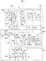
- FIG. 1 is a circuit diagram illustrating a configuration of the oscillation circuit according to the first embodiment.
- FIG. 2 is a waveform diagram illustrating the operation of the oscillation circuit according to the first embodiment.
- the oscillation circuit 10A according to the first embodiment includes a constant current generation circuit 1, a comparison reference voltage generation circuit 2, and an oscillation circuit core unit OSC1.
- the constant current generation circuit 1 includes a PMOS transistor M1, an operational amplifier (differential amplifier) A1, and a resistor R1. In the PMOS transistor M1, its drain terminal is connected to GND via the resistor R1, and its source terminal is connected to the power supply terminal VCC.
- the logic circuit L1 has a set signal input terminal S, a reset signal input terminal R, an output terminal Q, and an inverted output terminal QB. The logic circuit L1 outputs a high level signal to the output terminal Q during a period from when the rising edge is input to the set signal input terminal S to when the rising edge is input to the reset signal input terminal R, and is reset.
- a low level signal is output to the output terminal Q.
- the logic circuit L1 outputs a signal having a polarity obtained by inverting the signal output from the output terminal Q to the inverting output terminal QB.
- the non-inverting input terminal (+) is connected to the connection point (node N1) between the capacitor C1 and the drain terminal of the PMOS transistor M3, the inverting input terminal ( ⁇ ) is output to the output terminal VR, and the output is output to the logic circuit L1.
- each of the capacitor C1 and the capacitor C2 is connected to the GND.
- the present invention is not limited to this.
- the capacitor C1 and the capacitor C2 may be connected to the power supply terminal VCC instead of the GND.
- connection order of the inverting input ( ⁇ ) and the non-inverting input (+) of the comparators CMP1 and CMP2, and the signal polarity of the set signal input terminal S and the reset signal input terminal R of the logic circuit L1 are also configured for convenience of explanation.
- the present invention is not limited to this configuration as long as an operation function described below can be obtained.
- the current value of the current I1 is a constant current that does not depend on the voltage applied to the power supply terminal VCC, as is apparent from the equation (1). Since the PMOS transistor M2 in the comparison reference voltage generation circuit 2 is in a current mirror relationship with the PMOS transistor M1 in the constant current generation circuit 1, the drain current I2 of the PMOS transistor M2 is also a constant current. Therefore, the potential drop of the resistor R2 is also a constant voltage. That is, a constant comparison reference voltage is output to the output terminal VR.
- ⁇ is a mirror ratio between the PMOS transistor M1 and the PMOS transistor M2.
- the PMOS transistor M3 and the PMOS transistor M4 also have a current mirror relationship with the PMOS transistor M1 in the constant current generation circuit 1, so that they function as a constant current source.
- ⁇ is a mirror ratio of the PMOS transistor M1, the PMOS transistor M3, and the PMOS transistor M4.
- the NMOS transistor M6 transitions to the ON state, short-circuits both terminals of the capacitor C2, and the capacitor C2 is discharged.
- the potential of the terminal (node N2) of the capacitor C2 that has been charged by the drain current I4 of the PMOS transistor M4 until just before is lowered toward GND (0 V) as shown in FIG. become.
- the output of the comparator CMP1 is inverted to the high level, the high level is output to the inversion output terminal QB of the logic circuit L1, thereby maintaining the on state of the NMOS transistor M6.
- the potential of the terminal of the capacitor C2 (node N2) is substantially fixed at GND.
- the output of the comparator CMP1 and the output of the logic circuit L1 are inverted after the potential of the terminal (node N1) of the capacitor C1 reaches the comparison reference voltage (V R ).
- V R comparison reference voltage
- td1 A certain finite delay time is required.
- the response of the logic circuit L1 generally composed of a CMOS logic gate or the like is sufficiently faster than the response of the comparator CMP1, so that most of the delay time (td1) occupies the response time of the comparator CMP1.
- the comparator CMP2 has the same circuit configuration as the comparator CMP1. Also, it is assumed that the PMOS transistor constants are set such that the drain currents I3 and I4 of the PMOS transistor M3 and the PMOS transistor M4 are the same current. By doing so, the delay similar to that on the comparator CMP1 side until the output of the comparator CMP2 and the output of the logic circuit L1 are inverted after the potential of the terminal (node N2) of the capacitor C2 reaches the comparison reference voltage (V R ). Time (td2) is required.
- the NMOS transistor M5 transitions to the OFF state in response to the inversion of the output terminal Q of the logic circuit L1 to the low level, and the drain current I3 of the PMOS transistor M3 again causes the capacitor Charging of C1 is started.
- the state is equivalent to the state of timing A. Thereafter, the operations of charging the capacitor C1 and shorting the capacitor C2, and shorting the capacitor C1 and charging the capacitor C2 as described above are repeated alternately. Become.
- the oscillation period (T) is changed from the comparator CMP1 output inversion on the capacitor C1 side to the next comparator CMP1 output inversion, or the capacitor C2. This corresponds to the period from the inversion of the comparator CMP2 output to the next comparator CMP2 output inversion.
- the charging period (Tc2) of the capacitor C2 + the delay time (td2) represents the half period of the oscillation period (T), and the charging period (Tc1) of the capacitor C1.
- the remaining half cycle is formed by the + delay time (td1), and the discharge time due to the short circuit of the capacitor C1 and the capacitor C2 by the NMOS transistor M5 and the NMOS transistor M6 does not affect the oscillation cycle (T).
- the capacitors C1 and C2 have the same capacitance, the PMOS transistor M3 and the PMOS transistor M4 are set to the same constant, and the comparators CMP1 and CMP2 are configured by the same circuit, the capacitors The charging period (Tc1) of C1 and the charging period (Tc2) of the capacitor C2 are substantially equal, and the delay time (td1) related to the output inversion of the comparator CMP1 and the delay time (td2) related to the output inversion of the comparator CMP2 are almost the same.
- the capacitance value of the capacitor C1 (and capacitor C2) is C
- T C C ⁇ V R / I 3 (4)
- the time component related to the discharge can be prevented from affecting the oscillation cycle, and therefore, even in a relatively high frequency region. Oscillation cycle fluctuations with respect to parameter fluctuations such as temperature fluctuations can be suppressed, and an oscillation circuit superior in ensuring oscillation frequency accuracy can be obtained.
- an oscillation pulse with a duty of approximately 50% can be obtained.
- the duty of the oscillation pulse refers to the ratio of the high level period of the oscillation pulse to the oscillation period (T).
- the oscillation period can be obtained without depending on the voltage of the reference voltage input terminal VREF, for example, some reference voltage output such as a band gap circuit configured on the same semiconductor substrate is used. Even in this case, even if the reference voltage output varies or varies due to temperature, the influence can be canceled, so that an oscillation circuit suitable for ensuring the oscillation frequency accuracy can be obtained.
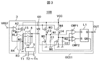
- FIG. 3 is a circuit diagram showing a configuration of an oscillation circuit according to the first modification.
- the oscillation circuit 10B according to the first modification is obtained by replacing the constant current generation circuit 1 and the comparison reference voltage generation circuit 2 of the oscillation circuit 10A according to the first embodiment with a bias circuit 3. That is, the oscillation circuit core part of the oscillation circuit 10B has the same configuration as the oscillation circuit core part OCS1 of the oscillation circuit 10A. However, the bias output terminal G0 to which the gate terminals of the PMOS transistor M3 and the PMOS transistor M4 are connected and the output terminal VR for sending the comparison reference voltage VR are both provided by the bias circuit 3.
- the bias circuit 3 includes a ladder resistor RL2, a PMOS transistor M7, an operational amplifier A2, an analog switch circuit 4, and a decoder circuit 5.
- the bias circuit 3 has functions of a constant current generation circuit and a reference voltage generation circuit.
- the ladder resistor RL2, the analog switch circuit 4, and the decoder circuit 5 constitute a trimming circuit that adjusts the reference voltage value. That is, the bias circuit 3 has a reference voltage trimming function.
- the ladder resistor RL2 is configured such that a plurality of unit resistors are connected in series and one end of the lowest unit resistor is connected to the GND so that a divided voltage output can be taken out from an arbitrary connection point of each unit resistor.
- the analog switch circuit 4 selectively sends each divided output of the ladder resistor RL2 to the output terminal VR.
- the decoder circuit 5 controls on / off of each switch in the analog switch circuit 4 in accordance with the n-bit frequency trimming signal input terminals T1 to Tn and the input signals of the frequency trimming signal input terminals T1 to Tn.
- the current I5 is a constant current that does not depend on the voltage applied to the power supply terminal VCC, like the current I1 of the first embodiment.
- any one of the switches in the analog switch circuit 4 is selectively turned on to the output terminal VR by the input signals of the frequency trimming signal input terminals T1 to Tn, and the output of the ladder resistor RL2 to which the selected switch is connected. Pressure output is delivered.
- the voltage sent to the output terminal VR becomes a comparison reference voltage for the comparators CMP1 and CMP2, and determines the charging time (T C ) of the capacitors C1 and C2.
- the oscillation operation of this modification uses the charging time of the capacitor C1 and the capacitor C2 by the PMOS transistor M3 and the PMOS transistor M4.
- the outline of the operation is shown in the waveform diagram of FIG. It is the same as that.
- T C The charging time (T C ) of the capacitor C1 is expressed by the equation (4).
- ⁇ represents the mirror ratio between the PMOS transistor M7 and the PMOS transistor M3.
- the oscillation period (T) is calculated by assuming that the response delay time of the comparators CMP1 and CMP2 is td.
- an oscillation circuit that can adjust the oscillation frequency can be obtained.
- the functions related to the frequency trimming input signal terminals T1 to Tn shown in the present embodiment are not limited to the configuration of the present embodiment, and are provided in, for example, the comparison reference voltage generation circuit 2 in the first embodiment of FIG. Is also possible.
- the resistor R2 may be configured in the form of a ladder resistor.
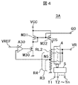
- FIG. 4 is a diagram illustrating a configuration of a bias circuit according to the second modification. Also, the configuration of the bias circuit 3 is not limited to the configuration shown in FIG. 3, and may be configured as shown in FIG. 4, for example.
- the PMOS transistor M32 its source terminal is connected to the power supply terminal VCC, and its gate terminal is connected to the gate terminal of the PMOS transistor M31 to form a current mirror with the PMOS transistor M31.
- the ladder resistor RL2 a plurality of unit resistors are connected in series, one end of the uppermost unit resistor is connected to the drain terminal of the PMOS transistor M32, and one end of the lowermost unit resistor is connected to the GND.
- the partial pressure output can be taken out from the point.
- the analog switch circuit 4 selectively sends each divided output of the ladder resistor to the output terminal VR.
- the decoder circuit 5 controls on / off of each switch in the analog switch circuit 4 in accordance with the n-bit frequency trimming signal input terminals T1 to Tn and the input signals of the frequency trimming signal input terminals T1 to Tn.
- the non-inverting input terminal (+) is connected to the reference voltage input terminal VREF
- the inverting input terminal ( ⁇ ) is an arbitrary divided output of the ladder resistor and the resistance value viewed from GND is R 3
- the output terminal is connected to the point (node N5) to the gate terminal of the NMOS transistor M30.
- FIG. 5 is a circuit diagram illustrating a configuration of the oscillation circuit according to the second embodiment.
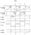
- FIG. 6 is a waveform diagram showing the operation of the oscillation circuit.
- the oscillation circuit 10C includes a power supply terminal VD1, a constant current bias source IB0, and an oscillation circuit core unit OSC2.
- the oscillation circuit core unit OSC2 includes a PMOS transistor M16, a PMOS transistor M17, and an NMOS transistor M18.
- the source terminal is connected to the power supply terminal VD1
- the drain terminal is connected to the constant current bias source IB0
- the gate terminal and the drain terminal are short-circuited.
- the PMOS transistor M17 its source terminal is connected to the power supply terminal VD1
- its gate terminal is connected to the gate terminal of the PMOS transistor M16.
- the oscillation circuit core unit OSC2 includes PMOS transistors M8 and M9, NMOS transistors M14 and M15, and capacitors C1, C2, C3, and C4.
- PMOS transistor M8 and M9 In the PMOS transistor M8, its drain terminal is connected to the capacitor C1, its source terminal is connected to the power supply terminal VD1, and its gate terminal is connected to the gate terminal of the PMOS transistor M16.
- PMOS transistor M9 In the PMOS transistor M9, its drain terminal is connected to the capacitor C2, its source terminal is connected to the power supply terminal VD1, and its gate terminal is connected to the gate terminal of the PMOS transistor M16.
- NMOS transistor M14 In the NMOS transistor M14, its drain terminal is connected to the capacitor C3, its source terminal is connected to GND, and its gate terminal is connected to the gate terminal of the NMOS transistor M18.
- NMOS transistor M15 In the NMOS transistor M15, its drain terminal is connected to the capacitor C4, its source terminal is connected to GND, and its gate terminal is connected to the gate terminal of the NMOS transistor M18.
- the oscillation circuit core unit OSC2 includes NMOS transistors M10 and M11, PMOS transistors M12 and M13, a logic circuit L1, a comparator CMP1, and a comparator CMP2.
- NMOS transistor M10 its drain terminal is connected to the drain terminal of the PMOS transistor M8, its source terminal is connected to GND, and its gate terminal is connected to the output terminal Q of the logic circuit L1.
- NMOS transistor M11 its drain terminal is connected to the drain terminal of the PMOS transistor M9, its source terminal is connected to GND, and its gate terminal is connected to the inverting output terminal QB of the logic circuit L1.
- the non-inverting input terminal (+) is connected to the connection point (node N1) between the drain terminal of the PMOS transistor M8 and the capacitor C1
- the inverting input terminal ( ⁇ ) is connected to the drain terminal of the NMOS transistor M14 and the capacitor C3.
- the non-inverting input terminal (+) is connected to the connection point (node N2) between the drain terminal of the PMOS transistor M9 and the capacitor C2, and the inverting input terminal ( ⁇ ) is connected to the drain terminal of the NMOS transistor M15 and the capacitor C4.
- the reset signal input terminal R of the logic circuit L1 is connected to the reset signal input terminal R of the logic circuit L1.
- the output terminal Q of the logic circuit L1 is connected to the oscillation output terminal OUT.
- the oscillation output may be taken out from the output terminal QB of the logic circuit L1.
- a signal output from the output terminal Q is referred to as a first control signal
- a signal output from the output terminal QB is referred to as a second control signal.
- FIG. 6A shows the potentials of the terminals of the capacitors C1 and C3 (nodes N1 and N3)
- FIG. 6B shows the potential of the terminals of the capacitors C2 and C4 (nodes N2 and N4)
- FIG. 6C shows the potential of the comparator CMP1.
- D is the output voltage of the comparator CMP2
- e is the voltage at the output terminal Q (oscillation output terminal OUT) of the logic circuit L1
- (f) is the inverted output of the logic circuit L1.
- the voltage at the terminal QB is shown.
- V D1 a constant voltage
- IB0 the current I6 flowing through the PMOS transistor M16 by the constant current bias source IB0
- the currents I8 and I9 flowing in the PMOS transistor M8 and the PMOS transistor M9, which are in a current mirror relationship with the PMOS transistor M16 are constant currents.
- the current I7 flowing through the PMOS transistor M17 that is in a current mirror relationship with the PMOS transistor M16 is a constant current.
- the NMOS transistor M10 and the NMOS transistor M11 have a current driving capability that is sufficiently larger than the currents I8 and I9 from the PMOS transistor M8 and the PMOS transistor M9. It is assumed that the terminal (node N1) and the terminal of the capacitor C2 (node N2) are short-circuited to GND, and the potential of these terminals (nodes N1 and N2) can be pulled down to almost GND.
- the PMOS transistor M12 and the PMOS transistor M13 also have a current driving capability that is sufficiently larger than the currents I10 and I11 in the NMOS transistor M14 and NMOS transistor M15.
- capacitors C1, C2, C3, and C4 are set to have the same capacitance value C, and currents I8, I9, I10, and I11 are set to have the same current value. To do.
- both the NMOS transistor M10 and the PMOS transistor M12 are in the ON state, so that the potential of the terminal of the capacitor C1 (node N1) is almost GND (0 V) and the terminal potential of the capacitor C3. Is substantially fixed at V D1 .
- the capacitor C1 starts to be charged with the current I8, and its terminal voltage rises linearly toward V D1 .
- the discharge by the current I10 is started from that time, and the potential of the terminal (node N1) decreases linearly toward GND (0V).
- “decreasing linearly” means that the decrease time between the predetermined potentials is substantially constant.
- charging is a bias application in the direction in which the potential difference between both terminals of the capacitor is expanded, and discharging is only a bias application in a direction in which the potential difference between both terminals of the capacitor is reduced.
- the relationship between the capacitor and the charge / discharge operation of each capacitor is not limited to the description of this embodiment. For example, if one end of the capacitor C1 is connected to the power supply terminal VD1 instead of GND, the capacitor C1 is “discharged” by the current I8, and the terminal voltage rises linearly toward V D1. .
- the NMOS transistor M11 which is a short circuit of the capacitor C2 has its gate terminal transitioned to the high level and turned on, and the PMOS transistor M13 which is a short circuit of the capacitor C4 is The gate terminal transitions to the low level and also transitions to the on state. Therefore, after timing C, the terminal of the capacitor C2 (node N2) is pulled down to GND, and the terminal of the capacitor C4 (node N4) is pulled up to V D1 .
- the potential of the terminal of the capacitor C1 (node N1) and the potential of the terminal of the capacitor C3 (node N3) Since the time required to transition to 1/2 voltage of V D1 is equal, the potential of the terminal of the capacitor C1 (node N1) and the potential of the terminal of the capacitor C3 (node N3) are respectively set to 1/2 voltage of V D1. It will cross when it reaches.
- the non-inverting input terminal (+) side of the comparator CMP1 is lower than the inverting input terminal ( ⁇ ) side. For this reason, the output of the comparator CMP1 outputs a low level.
- the comparator CMP1 passes through the response delay time (td1 ′) of the comparator CMP1 from the time when the potential of the terminal of the capacitor C1 (node N1) and the potential of the terminal of the capacitor C3 (node N3) cross, that is, the same potential. The output is inverted to the high level. This corresponds to the state of timing D in FIG.
- the potentials of the terminals are substantially fixed to GND and V D1 by the respective short-circuit circuits of the NMOS transistor M11 and the PMOS transistor M13.
- the capacitor C2 starts to be charged with the current I9, and the potential of the terminal of the capacitor C2 (node N2) goes from GND (0V) to V D1 .
- the capacitor C4 starts discharging with the current I11, and the potential of the terminal of the capacitor C4 (node N4) decreases linearly from V D1 to GND (0 V). If the current I9 and the current I11 have the same current value, the terminals of the capacitors C2 and C4 (nodes N2 and N4) with a voltage of 1/2 of V D1 as in the case of the capacitors C1 and C3 after the timing C. Will cross each other.
- the comparator CMP2 receives the response delay time (td2) as in the case of the comparator CMP1. After that, the output is inverted to High level. This corresponds to the timing C ′ in FIG.
- (C) Timing C ′ At this timing C ′, when the output of the comparator CMP2 is inverted to the high level and the inverted output terminal QB side of the logic circuit L1 transitions to the high level and the output terminal Q side transitions to the low level, the NMOS transistor M10 and the PMOS transistor M12 are turned off. After the transition to the state, charging of the capacitor C1 and discharging of the capacitor C3 by the currents I8 and I10 are started again.
- the NMOS transistor M11 and the PMOS transistor M13 are turned on, the capacitor C2 terminal (node N2) is pulled down to GND, and the capacitor C4 terminal (node N4) is pulled up to V D1 , thereby the terminal of the capacitor C2 ( The potential of the terminal of the capacitor C4 (node N4) with respect to the potential of the node N2) rises rapidly, and the output of the comparator CMP2 returns to the low level.
- This state is equivalent to the state at the timing C described above, and the operation described above is repeated thereafter.
- the oscillation output terminal OUT is taken out from the output terminal Q of the logic circuit L1, and the period from the inversion of the comparator CMP1 output (or the comparator CMP2 output) to the high level until the inversion to the next high level is the oscillation period (T ).
- the High period and Low period of the output terminal Q are formed by the time related to charging / discharging of the capacitor C1 / capacitor C3 and the time related to charging / discharging of the capacitor C2 / capacitor C4, respectively.
- the time width can be set, and therefore, an oscillation pulse of approximately 50% duty can be obtained.
- the response delay times (td ′) of the comparators CMP1 and CMP2 in order for each comparator output to invert to the high level, the terminal potential on the non-inverting input terminal (+) side must be on the inverting input terminal ( ⁇ ) side. It is necessary to exceed the terminal potential, and the larger the potential difference between them, the shorter the response delay time until output inversion.
- the potential of the terminal (node N1) of the capacitor C1 that is rising due to charging (or the potential of the terminal of the capacitor C2 (node N2)) and the terminal of the capacitor C3 that is falling due to discharging (node N3) Since the configuration is such that the potential (or the potential of the terminal of the capacitor C4 (node N4)) is compared, the input potential difference is more compared to the case where the comparison is made with a constant comparison reference voltage (V R ) as in the first embodiment. It can be expanded early, and the response delay time (td ′) can be shortened.
- td which is a component related to the response delay time of the comparator in the expressions (6) and (10) representing the oscillation period (T) described in the first embodiment and the first modification, is compressed, and the comparator changes due to parameter fluctuations such as temperature fluctuations. Even if the response delay time fluctuates, since the ratio of td in the oscillation period (T) can be reduced, the fluctuation of the oscillation frequency can be suppressed as compared with the first embodiment.
- the response delay time of the comparator can be shortened, it is possible to obtain an oscillation circuit that is superior in ensuring the oscillation frequency accuracy.
- the PMOS transistors M8 and M9 and the NMOS transistors M14 and M15 constituting the constant current sources for driving the capacitors C1 and C2 to charge and driving the capacitors C3 and C4 to discharge are all connected to the capacitor terminals (nodes N1, N2, N3, N3,. Because of the configuration directly connected to N4), when any of the NMOS transistors M10 and M11 and the PMOS transistors M12 and M13 constituting the short circuit switch is turned on, the output current of the constant current source is in the on state. Bypass to the short-circuit switch side. Since this is a reactive current, it is originally advantageous to cut it off from the viewpoint of current consumption. However, if a configuration that cuts off this is used, the following problems occur.
- a cut-off switch is provided between the drain terminal of the PMOS transistor M8 and the terminal (node N1) of the capacitor C1, and the NMOS transistor is a short-circuit switch.
- the cutoff switch is turned off when M10 is turned on. This can be easily realized by providing a PMOS transistor as the cutoff switch and directly connecting the gate terminal to the gate terminal of the NMOS transistor M10.
- the NMOS transistor M10 is turned off and at the same time the cutoff switch is turned on. At that moment, the charge charged in the parasitic capacitance is changed. Distribution to the capacitor C1 side (so-called charge sharing occurs) changes the potential of the terminal (node N1) of the capacitor C1. As a result, the detection timing by the comparator CMP1 varies, and the oscillation period varies.
- the present embodiment and other embodiments also employ a configuration capable of suppressing oscillation frequency fluctuations due to the charge share as a configuration in which a constant current source is directly connected to each capacitor.
- the terminal voltages of the charge drive side capacitor and the discharge drive side capacitor that are driven simultaneously are compared with each other to be compared with a constant comparison reference voltage (V R ).
- V R a constant comparison reference voltage
- the comparator detection timing period must be the same in order to obtain the same oscillation period, so whether the voltage amplitude itself during charge (or discharge) drive should be doubled after doubling the capacitor drive current
- the comparison reference voltage (V R ) is used as the voltage (or GND voltage) of the power supply terminal VD1, and the voltage change width within the comparator detection timing cycle is doubled.
- V R a constant comparison reference voltage
- Modification 3 provides an oscillation circuit that can adjust the oscillation frequency and is more advantageous for ensuring the oscillation frequency accuracy.
- FIG. 7 is a circuit diagram showing a configuration of an oscillation circuit according to the third modification.
- the oscillation circuit core unit OSC3 of the oscillation circuit 10D according to Modification 3 has the same configuration as that of the oscillation circuit core unit OSC2 of the oscillation circuit 10C of Example 2 except for the logic circuit L2, the comparator CMP3, and the comparator CMP4.
- the oscillation circuit 10 ⁇ / b> D has a bias circuit 6. The difference between the oscillation circuit 10D and the oscillation circuit 10C will be described below.
- the bias circuit 6 has a power supply terminal VCC, a reference voltage input terminal VREF, and output terminals IB, VD1, and VD2.
- the inverting input terminal ( ⁇ ) is connected to the connection point (node N1) between the drain terminal of the PMOS transistor M8 and the capacitor C1, and the non-inverting input terminal (+) is connected to the drain terminal of the NMOS transistor M14 and the capacitor C3.
- the inverting input terminal ( ⁇ ) is connected to the connection point (node N2) between the drain terminal of the PMOS transistor M9 and the capacitor C2, and the non-inverting input terminal (+) is connected to the drain terminal of the NMOS transistor M15 and the capacitor C4.
- the output terminal Q of the logic circuit L2 is connected to the oscillation output terminal OUT. The oscillation output may be taken out from the output terminal QB of the logic circuit L2.
- the bias circuit 6 includes a ladder resistor RL4, a PMOS transistor M7, an operational amplifier A2, an analog switch circuit 4, a decoder circuit 5, a PMOS transistor M19, an NMOS transistor M20, an NMOS transistor M21, an operational amplifier A3, and a PMOS.
- the transistor M22, the operational amplifier A4, and the PMOS transistor M23 are included.
- the bias circuit 6 has the functions of a constant current generation circuit and a reference voltage generation circuit, like the bias circuit 3.
- the ladder resistor RL4, the analog switch circuit 4, and the decoder circuit 5 constitute a trimming circuit that adjusts the reference voltage value. That is, the bias circuit 6 has a reference voltage trimming function.
- the ladder resistor RL4 a plurality of unit resistors are connected in series and one end of the lowermost unit resistor is connected to the GND so that a divided voltage output can be taken out from an arbitrary connection point of each unit resistor.
- the PMOS transistor M7 its drain terminal is connected to one end (node N8) of the uppermost unit resistor of the ladder resistor RL4, and its source terminal is connected to the power supply terminal VCC.
- the inverting input terminal ( ⁇ ) is the reference voltage input terminal VREF
- the non-inverting input terminal (+) is an arbitrary divided output of the ladder resistor RL4, and the resistance value viewed from GND is R 5 .
- the output terminal is connected to the connection point (node N6) to the gate terminal of the PMOS transistor M7.
- the operational amplifiers A2, A3, and A4 operate between the potential of the power supply terminal VCC and GND.
- the analog switch circuit 4 selectively outputs each divided voltage output of the ladder resistor RL4.
- the decoder circuit 5 controls on / off of each switch in the analog switch circuit 4 according to the input signals of the n-bit frequency trimming signal input terminals T1 to Tn and the frequency trimming signal input terminals T1 to Tn. .
- the source terminal is connected to the power supply terminal VCC and the gate terminal is connected to the output terminal of the operational amplifier A2, and the PMOS transistor M7 and the current mirror are in a relationship.
- NMOS transistor M20 In the NMOS transistor M20, its drain terminal is connected to the drain terminal of the PMOS transistor M19, its source terminal is connected to GND, and its gate terminal is short-circuited to the drain terminal.
- the drain terminal In the NMOS transistor M21, the drain terminal is connected to the output terminal IB, the source terminal is connected to GND, the gate terminal is connected to the gate terminal of the NMOS transistor M20, and the NMOS transistor M20 has a current mirror relationship.
- operational amplifier A3 In the operational amplifier A3, its inverting input terminal ( ⁇ ) is connected to the output of the analog switch circuit 4, and its non-inverting input terminal (+) is connected to the output terminal VD1.
- the PMOS transistor M22 its source terminal is connected to the power supply terminal VCC, its drain terminal is connected to the output terminal VD1, and its gate terminal is connected to the output terminal of the operational amplifier A3.
- the inverting input terminal ( ⁇ ) is connected to the connection point between the drain terminal of the PMOS transistor M7 and the uppermost unit resistor of the ladder resistor RL4, and the non-inverting input terminal (+) is connected to the output terminal VD2.
- the PMOS transistor M23 its source terminal is connected to the power supply terminal VCC, its drain terminal is connected to the output terminal VD2, and its gate terminal is connected to the output terminal of the operational amplifier A4.
- the logic circuit L2 includes a NAND gate G1, a NAND gate G2, an inverter G3, and an inverter G4.
- NAND gate G1 one of its input terminals is connected to the set signal input terminal S, and its output terminal is connected to the input terminal of the inverter G3.
- NAND gate G2 one of its input terminals is connected to the reset signal input terminal R, the other input terminal is connected to the output terminal of the NAND gate G1, and its output terminal is connected to the other input terminal of the NAND gate G1.
- the inverter G4 has its input terminal connected to the output terminal of the inverter G3, the output terminal of the inverter G3 is the inverted output terminal QB, and the output terminal of the inverter G4 is the output terminal Q.
- the logic circuit L2 outputs a high level signal to the output terminal Q during a period from when the falling edge is input to the set signal input terminal S to when the falling edge is input to the reset signal input terminal R.
- the logic circuit L2 outputs a low level signal to the output terminal Q during a period from when the falling edge is input to the reset signal input terminal R to when the falling edge is input to the set signal input terminal S.
- a signal having a polarity obtained by inverting the signal output of the output terminal Q is output to the inverted output terminal QB.
- a signal output from the output terminal Q is referred to as a first control signal
- a signal output from the output terminal QB is referred to as a second control signal.
- the source terminals of the PMOS transistors M8, M9, M12, M13, M16, and M17 are connected to the output terminal VD1 of the bias circuit 6, and the power supplies of the comparators CMP3 and CMP4 and the logic circuit L2 are output.
- the configuration is given from the terminal VD2. Providing two power sources in this way is not necessarily an essential matter, but its unique effect will be described in the following description of the operation.
- the charge / discharge time (T C ′) is expressed in a form that does not include the components of voltage (V D1 ) and constant current (I 6 ), but this is the voltage (V D1 ).
- the constant current (I 6 ) are in a constant proportional relationship as shown in the equation (14), and when it fluctuates with a component that does not depend on the proportional relationship, such as the above-described voltage fluctuation, discharge time (T C ') also it would lead to variation.
- the fluctuation of the charge / discharge time (T C ′) leads to the fluctuation of the oscillation period (T).
- T oscillation period
- Each of the output terminals VD1 of the bias circuit 6 according to the present modification is connected to the power supply terminal VD1 of the oscillation circuit 10C according to the second embodiment, and the output terminal IB of the bias circuit 6 is replaced with the constant current bias source IB0 to replace the PMOS transistor
- An oscillation circuit may be configured by connecting to the drain terminal of M16.
- the current mirror ratio with the NMOS transistor M20 may be effectively changed by changing the selection number of the collector terminals of the NMOS transistors M211 to M21i according to the input signals of the frequency trimming signal input terminals Tn + 1 to Tn + m.
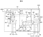
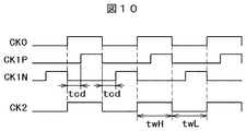
- FIG. 10 is a timing chart of the clock pulse generation circuit according to the third embodiment.
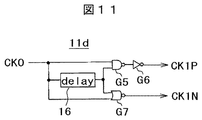
- the two-phase clock signals CK1P and CK1N have a delay time (tcd) on the rising side with respect to the oscillation output signal CK0 as described above.
- a two-phase clock signal is formed without overlapping the periods.
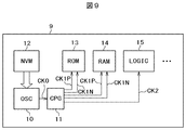
- the access control of the RAM module 14 is performed using the two-phase clock signals CLK1P and CLK1N, for example, the high-level period of the two-phase clock signal CK1P is set to the data line precharge in the RAM module 14. It is possible to perform read control such that the high-level period of the two-phase clock signal CK1N is allocated to the activation of the data read sense amplifier and the latch control of the sense amplifier output data.
Landscapes
- Engineering & Computer Science (AREA)
- Signal Processing (AREA)
- Physics & Mathematics (AREA)
- General Physics & Mathematics (AREA)
- Radar, Positioning & Navigation (AREA)
- Remote Sensing (AREA)
- Gyroscopes (AREA)
- Inductance-Capacitance Distribution Constants And Capacitance-Resistance Oscillators (AREA)
Abstract
比較的高周波域でも温度変動などのパラメータ変動に対して発振周波数精度を確保する発振回路を提供するために、発振回路は、電流によって充電駆動されその端子電圧が第1の方向に直線的に変化する第1のコンデンサと、第1のコンデンサの充電駆動に並行して電流によって放電駆動されその端子電圧が第1の方向とは逆方向の第2の方向に直線的に変化する第2のコンデンサと、を具備する。上記発振回路は、第1および第2のコンデンサの各端子電圧が交差する第1のタミングに基づいて発振周期を形成するようにされる。
Description
本開示は、発振回路に関し、コンデンサの充放電時定数を利用して発振周期を形成する発振回路に適用可能である。
コンデンサの充放電時定数を利用して発振周期を形成する発振回路は、例えば、特開2001-127592号公報(特許文献1)に開示されている。この発振回路は、任意の電圧に比例する定電流を生成する定電流生成部と、この定電流生成部で生成された定電流により充電されるコンデンサと、このコンデンサの充電電圧を基準電圧と比較し、この充電電圧が基準電圧を上回ったときに放電信号を生成し、この放電信号によりコンデンサの充電電荷を放電する放電部とを備え、この放電部で生成される放電信号を発振出力として取り出すようになっている。
特許文献1の図2に示されるように、発振周期(TS)は、充電時間(T)に放電信号幅(TP)を加えたものとなるが、特許文献1では、放電信号幅(TP)は充電時間(T)の1/1000程度であり、充電時間(T)を発振周期(TS)とみなしても実用上は問題ないとしている。しかし、特に高周波の発振出力を必要とする用途においては問題を生じることになる。
コンデンサ(C)の放電には必ず有限な時間幅が必要であり、これを10ns程度(=放電信号幅(TP))と仮定すると、発振周波数が100KHz(発振周期(TS)=10μs)程度であれば実用上の問題は無いとも考えられる。しかし、例えば20MHz(発振周期(TS)=50ns)程度の発振周波数を得ようとする場合においては、放電信号幅(TP)がその周期(TS)に対して20%の比率を占めることとなり、発振周波数精度確保の観点で放電信号幅(TP)の成分を無視することができなくなる。具体的には放電時間、すなわち放電信号幅(TP)は特許文献1の図1に示されるNMOSトランジスタ(N1)のオン抵抗に依存するため、温度およびコンパレータ(21)の出力の「H」レベル(=電源電圧(VCC)の電位)、さらにプロセスパラメータばらつき、などの影響を受けて変動することとなり、例えば20MHz±5%程度の発振周波数精度を広範な使用温度範囲や使用電源電圧範囲に亘って確保しようとすることは極めて困難となる。
また、特許文献1の図2においては、コンデンサ(C)の充電電圧が基準電圧(VIN)に到達した時点でコンパレータ(21)の出力が「H」レベルに反転し、コンパレータ(21)の検知遅れは無いものとして記載されている。しかし、実際にはその検知遅れ時間が存在し、これも高周波域での発振周波数精度確保の障害となる。具体的には、コンパレータ(21)の出力が「H」レベルに反転するには、その反転・非反転入力間の電位差が、コンパレータ(21)が感応できるレベルまで開く必要がある。しかし、その感応レベルもコンパレータ(21)の入力差動対を構成するMOSトランジスタのgmなどに依存するため、やはり上記パラメータ変動の影響を受けることになる。結果的に温度変動などのパラメータ変動によってコンパレータ(21)の検知応答時間も変動を来たすこととなり、発振周波数精度確保を図る上での障害となる。
そこで本開示は、数十MHz程度の高周波域でも発振周波数精度を有する発振回路を提供することを課題とする。
その他の課題と新規な特徴は、本開示の記述および添付図面から明らかになるであろう。
本開示のうち、代表的なものの概要を簡単に説明すれば、下記のとおりである。
すなわち、発振回路は、電流によって充電駆動されその端子電圧が第1の方向に直線的に変化する第1のコンデンサと、第1のコンデンサの充電駆動に並行して電流によって放電駆動されその端子電圧が第1の方向とは逆方向の第2の方向に直線的に変化する第2のコンデンサと、を具備する。第1および第2のコンデンサの各端子電圧が交差する第1のタミングに基づいて発振周期を形成するようにされる。
すなわち、発振回路は、電流によって充電駆動されその端子電圧が第1の方向に直線的に変化する第1のコンデンサと、第1のコンデンサの充電駆動に並行して電流によって放電駆動されその端子電圧が第1の方向とは逆方向の第2の方向に直線的に変化する第2のコンデンサと、を具備する。第1および第2のコンデンサの各端子電圧が交差する第1のタミングに基づいて発振周期を形成するようにされる。
上記発振回路によれば、発振周波数精度を確保することができる。
<実施の形態>
実施の形態のうち、代表的なものの概要を簡単に説明すれば、下記のとおりである。
(1)発振回路は、
電流によって充電駆動され、その端子電圧が第1の方向に直線的に変化する第1のコンデンサ(C1)と、
第1のコンデンサ(C1)の充電駆動とともに電流によって放電駆動され、その端子電圧が第1の方向とは逆方向の第2の方向に直線的に変化する第2のコンデンサ(C3)と、
を具備し、
第1および第2のコンデンサ(C1、C3)の各端子電圧が交差する第1のタミング(D)に基づいて発振周期を形成するようにされる。
(2)上記(1)の発振回路は、
第1のタイミング(D)に基づいて、第1のコンデンサ(C1)の端子電圧を第2の方向にプルダウンまたはプルアップし、第2のコンデンサ(C3)の端子電圧を第1の方向にプルアップまたはプルダウンする。
(3)上記(2)の発振回路は、
電流によって充電駆動されその端子電圧が第1の方向に直線的に変化する第3のコンデンサ(C2)と、
第3のコンデンサの充電駆動とともに電流によって放電駆動され、その端子電圧が第2の方向に直線的に変化する第4のコンデンサ(C4)と、
を具備し、
第3および第4のコンデンサ(C2、C4)の各端子電圧が交差する第2のタミング(C、C’)に基づいて発振出力を反転する。
(4)上記(3)の発振回路は、
第2のタイミング(C、C’)に基づいて、第3のコンデンサ(C2)の端子電圧を第2の方向にプルダウンまたはプルアップし、第4のコンデンサ(C4)の端子電圧を第1の方向にプルアップまたはプルダウンする。
(5)上記(4)の発振回路は、
第1の方向は第1の電源端子(VD1)の電位の方向であり、第2の方向は基準電位の方向であり、
第1の電源端子(VD1)の電圧値を調整する第1のトリミング回路(RL4、4、5)と、
第1および第3のコンデンサ(C1、C2)の端子を充電駆動する電流(I8、I9)の電流値と、第2および第4のコンデンサの端子(C3、C4)を放電駆動する電流(I10、I11)の電流値と、を調整する第2のトリミング回路(M20、M211、M212、M21i、7、8)と、
を具備する。
(6)半導体集積回路装置は、
上記(5)の発振回路(10)と、
第1および第2のトリミング回路のトリミングデータを格納する不揮発性メモリモジュール(12)と、
発振回路の発振出力パルスから生成したシステムクロックによって制御される論理回路(15)と、
を具備する。
(7)回転角検出装置は、
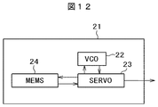
上記1から5のいずれか1つの発振回路(22)と、
発振回路(22)の発振出力パルスクロックによって制御されるサーボ(23)と、
サーボ(23)から駆動信号を受ける角速度検出素子(24)と、
を具備する。
(8)発振回路は、
第一の電源端子(VD1)と、
第一、第二の端子を有し、該第一の端子を基準電位に接続した第一のコンデンサ(C1)と、
第一のコンデンサ(C1)の第二の端子(N1)と第一の電源端子(VD1)との間に設けられた第一の定電流源(M8)と、
第一の制御信号に基づいて第一のコンデンサ(C1)の第二の端子(N1)と基準電位との間を短絡する第一の短絡回路(M10)と、
第一、第二の端子を有し、該第一の端子を基準電位に接続した第二のコンデンサ(C3)と、
第二のコンデンサ(C3)の第二の端子(N3)と基準電位との間に設けられた第二の定電流源(M14)と、
第一の制御信号に対して反転した極性を有する第二の制御信号に基づいて第二のコンデンサ(C3)の第二の端子(N3)と第一の電源端子(VD1)との間を短絡する第二の短絡回路(M12)と、
第一、第二の端子を有し、該第一の端子を基準電位に接続した第三のコンデンサ(C2)と、
第三のコンデンサ(C2)の第二の端子(N2)と第一の電源端子(VD1)との間に設けられた第三の定電流源(M9)と、
第二の制御信号に基づいて第三のコンデンサ(C2)の第二の端子(N2)と基準電位との間を短絡する第三の短絡回路(M11)と、
第一、第二の端子を有し、該第一の端子を基準電位に接続した第四のコンデンサ(C4)と、
第四のコンデンサ(C4)の第二の端子(N4)と基準電位との間に設けられた第四の定電流源(M15)と、
第一の制御信号に基づいて第四のコンデンサ(C4)の第二の端子(N4)と第一の電源端子(VD1)との間を短絡する第四の短絡回路(M13)と、
第一のコンデンサ(C1)の第二の端子電位と第二のコンデンサ(C3)の第二の端子電位とを比較する第一のコンパレータ(CMP1、CMP3)と、
第三のコンデンサ(C2)の第二の端子電位と第四のコンデンサ(C4)の第二の端子電位とを比較する第二のコンパレータ(CMP2、CMP4)と、
第一のコンパレータ(CMP1、CMP3)の比較出力と第二のコンパレータ(CMP2、CMP3)の比較出力とに基づき第一の制御信号および第二の制御信号を生成する論理回路(L1、L2)と、
を具備し、
論理回路(L1、L2)は、
第一のコンパレータ(CMP1、CMP3)が第一のコンデンサ(C1)の第二の端子電位と第二のコンデンサ(C3)の第二の端子電位との交差を検知して成した比較出力反転から第二のコンパレータ(CMP2、CMP4)が第三のコンデンサ(C2)の第二の端子電位と第四のコンデンサ(C4)の第二の端子電位との交差を検知して成した比較出力反転までの期間内は、第一の制御信号を第一の極性で、また第二の制御信号を第二の極性でそれぞれ出力し、
第二のコンパレータ(CMP2、CMP4)が第三のコンデンサ(C2)の第二の端子電位と第四のコンデンサ(C4)の第二の端子電位との交差を検知して成した比較出力反転から第一のコンパレータ(CMP1、CMP3)が第一のコンデンサ(C1)の第二の端子電位と第二のコンデンサ(C3)の第二の端子電位との交差を検知して成した比較出力反転までの期間内は、第一の制御信号を第二の極性で、また第二の制御信号を第一の極性でそれぞれ出力するように構成し、
第一の短絡回路(M10)は第一の制御信号の第一の極性で活性化し、
第二の短絡回路(M12)は第二の制御信号の第二の極性で活性化し、
第三の短絡回路(M11)は第二の制御信号の第一の極性で活性化し、
第四の短絡回路(M13)は第一の制御信号の第二の極性で活性化するように構成するとともに、第一または第二の制御信号を発振出力として利用する。
本開示において、定電流または定電流源とは、電流値はほぼ一定である電流または電流源であって、電流値の変動を許容する。その結果、例えば、発振周波数精度が所定範囲内(±5%)に収まる程度の変動を許容するものである。
以下、実施例および変形例について、図面を用いて説明する。ただし、以下の説明において、同一構成要素には同一符号を付し繰り返しの説明は省略する。
実施例1は、定電流によるコンデンサの充電時間を利用して発振周期を形成する発振回路において、温度変動などによる発振周期の変動を抑制し、数十MHz程度(20MHz~60MHz程度)と比較的高周波領域においてもその発振周波数精度を確保し得る発振回路を提供するものである。
図1は実施例1に係る発振回路の構成を示す回路図である。図2は実施例1に係る発振回路による動作を示す波形図である。
(構成)
実施例1に係る発振回路10Aは、定電流生成回路1と比較基準電圧生成回路2と発振回路コア部OSC1を有する。
定電流生成回路1は、PMOSトランジスタM1とオペアンプ(差動増幅器)A1と抵抗R1を有する。PMOSトランジスタM1において、そのドレイン端子を抵抗R1を介してGNDに、そのソース端子を電源端子VCCに、それぞれ接続する。オペアンプA1において、その反転入力端子(-)を参照電圧入力端子VREFに、その非反転入力端子(+)をPMOSトランジスタM1のドレイン端子と抵抗R1の接続点(ノードN7)に、その出力端子をPMOSトランジスタM1のゲート端子に、それぞれ接続する。定電流生成回路1において、オペアンプA1の出力端子とPMOSトランジスタM1のゲート端子の接続点をバイアス出力端子G0としている。オペアンプA1は電源端子VCCの電位とGNDとの間で動作する。
比較基準電圧生成回路2は、PMOSトランジスタM2と抵抗R2を有する。PMOSトランジスタM2において、そのドレイン端子を抵抗R2を介してGNDに、そのソース端子を電源端子VCCに、そのゲート端子を定電流生成回路1のバイアス出力端子G0に、それぞれ接続する。比較基準電圧生成回路2において、PMOSトランジスタM2のドレイン端子と抵抗R2との接続点を比較基準電圧の出力端子VRとしている。
発振回路コア部OSC1は、PMOSトランジスタ(第1の導電型のMOSトランジスタ)M3とNMOSトランジスタ(第2の導電型のMOSトランジスタ)M5とPMOSトランジスタM4とNMOSトランジスタM6と論理回路L1とコンパレータCMP1とコンパレータCMP2とコンデンサC1とコンデンサC2を有する。PMOSトランジスタM3において、そのドレイン端子をコンデンサC1に、そのソース端子を電源端子VCCに、そのゲート端子をバイアス出力端子G0に、それぞれ接続する。NMOSトランジスタM5において、そのドレイン端子をPMOSトランジスタM3のドレイン端子に、ソース端子を基準電位(以下、GNDと記す)にそれぞれ接続する。PMOSトランジスタM4において、そのドレイン端子をコンデンサC2に、そのソース端子を電源端子VCCに、そのゲート端子をバイアス出力端子GOに、それぞれ接続する。NMOSトランジスタM6において、そのドレイン端子をPMOSトランジスタM4のドレイン端子に、そのソース端子をGNDに、それぞれ接続する。論理回路L1はセット信号入力端子Sとリセット信号入力端子Rと出力端子Qと反転出力端子QBとを有する。論理回路L1は、セット信号入力端子Sに立上りエッジが入力されてからリセット信号入力端子Rに立上りエッジが入力されるまでの期間は出力端子Qにハイ(High)レベルの信号出力を行い、リセット信号入力端子Rに立上りエッジが入力されてからセット信号入力端子Sに立上りエッジが入力されるまでの期間は出力端子Qにロウ(Low)レベルの信号出力を行う。また、論理回路L1は、反転出力端子QBに出力端子Qの信号出力を反転した極性の信号出力を行う。コンパレータCMP1において、その非反転入力端子(+)をコンデンサC1とPMOSトランジスタM3のドレイン端子との接続点(ノードN1)に、反転入力端子(-)を出力端子VRに、その出力を論理回路L1のセット信号入力端子Sに、それぞれ接続する。コンパレータCMP2において、その非反転入力端子(+)をコンデンサC2とPMOSトランジスタM4のドレイン端子との接続点(ノードN2)に、反転入力端子(-)を出力端子VRに、その出力を論理回路L1のリセット信号入力端子Rに、それぞれ接続する。論理回路L1の出力端子Qを発振出力端子OUT及びNMOSトランジスタM5のゲート端子に、また反転出力端子QBをNMOSトランジスタM6のゲート端子に、それぞれ接続している。なお、論理回路L1の出力端子QBから発振出力を取り出してもよい。コンパレータCMP1、CMP2および論理回路L1は電源端子VCCの電位とGNDとの間で動作する。
なお、図1においては、コンデンサC1及びコンデンサC2の一端をいずれもGNDへ接続しているが、これに限定されるものではなく、例えばGNDに替えて電源端子VCCへ接続しても構わない。
またコンパレータCMP1、コンパレータCMP2の反転入力(-)、非反転入力(+)の接続順や、論理回路L1のセット信号入力端子S、リセット信号入力端子Rの信号極性についても説明の便宜上の構成に過ぎず、以下に説明する動作機能が得られるものであれば、当該構成に限定されない。
(動作)
以下、本実施例の動作について、図2の波形図を参照しながら説明する。図2(a)はコンデンサC1の端子(ノードN1)の電位、同図(b)はコンデンサC2の端子(ノードN2)の電位、同図(c)はコンパレータCMP1の出力電圧、同図(d)はコンパレータCMP2の出力電圧、同図(e)は論理回路L1の出力端子Q(発振出力端子OUT)の電圧、同図(f)は論理回路L1の反転出力端子QBの電圧を示している。
以下、本実施例の動作について、図2の波形図を参照しながら説明する。図2(a)はコンデンサC1の端子(ノードN1)の電位、同図(b)はコンデンサC2の端子(ノードN2)の電位、同図(c)はコンパレータCMP1の出力電圧、同図(d)はコンパレータCMP2の出力電圧、同図(e)は論理回路L1の出力端子Q(発振出力端子OUT)の電圧、同図(f)は論理回路L1の反転出力端子QBの電圧を示している。
まず、定電流生成回路1において、オペアンプA1の非反転入力(+)へ接続されている抵抗R1の端子電圧は、反転入力(-)に接続する参照電圧端子VREFの印加電圧と等しくなるようにフィードバック制御される。よって抵抗R1及びPMOSトランジスタM1に流れる電流I1の電流値をI1とすると、
I1=VREF/R1 ・・・(1)
と表される。ここで、VREFは参照電圧入力端子VREFの印加電圧、R1は抵抗R1の抵抗値である。
I1=VREF/R1 ・・・(1)
と表される。ここで、VREFは参照電圧入力端子VREFの印加電圧、R1は抵抗R1の抵抗値である。
電流I1の電流値は、式(1)からも明らかなように電源端子VCCの印加電圧には依存しない定電流となる。また、比較基準電圧生成回路2内のPMOSトランジスタM2は、定電流生成回路1内のPMOSトランジスタM1とカレントミラーの関係にあるから、PMOSトランジスタM2のドレイン電流I2も定電流となる。よって抵抗R2の電位降下も一定電圧となる。すなわち、出力端子VRには一定の比較基準電圧が出力される。その比較基準電圧をVR、抵抗R2の抵抗値をR2、ドレイン電流I2の電流値をI2とすれば、
VR=I2×R2=α×I1×R2=α×VREF×R2/R1 ・・・(2)
と表される。ここで、αはPMOSトランジスタM1とPMOSトランジスタM2とのミラー比である。
VR=I2×R2=α×I1×R2=α×VREF×R2/R1 ・・・(2)
と表される。ここで、αはPMOSトランジスタM1とPMOSトランジスタM2とのミラー比である。
また、PMOSトランジスタM3及びPMOSトランジスタM4も定電流生成回路1内のPMOSトランジスタM1とカレントミラーの関係にあるから、それらは定電流源として機能する。PMOSトランジスタM3及びPMOSトランジスタM4の各ドレイン電流I3、I4の電流値をそれぞれI3、I4とすると、
I3(=I4)=β×I1=β×VREF/R1 ・・・(3)
と表される。ここで、βはPMOSトランジスタM1とPMOSトランジスタM3及びPMOSトランジスタM4のミラー比である。
I3(=I4)=β×I1=β×VREF/R1 ・・・(3)
と表される。ここで、βはPMOSトランジスタM1とPMOSトランジスタM3及びPMOSトランジスタM4のミラー比である。
次に発振動作について説明する。
(a)タイミングA~タイミングB
いま、論理回路L1の出力端子QがLowレベルへ遷移すると同時に、反転出力端子QBがHighレベルへ遷移するとする。このときNMOSトランジスタM5は、そのゲート端子がLowレベルへ遷移することにより、オン状態からオフ状態へ遷移する。また、NMOSトランジスタM6は、そのゲート端子がHighレベルへ遷移することにより、オフ状態からオン状態へ遷移する。ここで、NMOSトランジスタM5の電流駆動能力は、PMOSトランジスタM3のドレイン電流I3に比べて十分大きく、そのオン状態においては、コンデンサC1の両端子間をほぼ同電位とする短絡回路として機能し得るものとする。なお、コンデンサC2側におけるNMOSトランジスタM6もNMOSトランジスタM5と同様、PMOSトランジスタM4のドレイン電流I4に比べて十分な大きさの電流駆動能力を有しており、コンデンサC2の短絡回路として機能し得るものとする。
よって、上記の如くNMOSトランジスタM5がオン状態からオフ状態へ遷移する時点では、コンデンサC1の端子(ノードN1)の電位はほぼGNDにあり、その状態からPMOSトランジスタM3によるコンデンサC1への充電電流の供給が開始される。これは図2の波形図におけるタイミングAの状態に相当し、PMOSトランジスタM3のドレイン電流I3は上記のように定電流であるため、タイミングA以降コンデンサC1の端子(ノードN1)の電位は図2(a)に記載のように直線的に上昇することになる。ここで、「直線的に上昇する」とは、所定電位間の上昇時間がほぼ一定であることを意味する。
一方、コンデンサC2側においては、NMOSトランジスタM6がオン状態へ遷移し、コンデンサC2の両端子間を短絡し、コンデンサC2は放電される。これによって直前までPMOSトランジスタM4のドレイン電流I4によって充電されていたコンデンサC2の端子(ノードN2)の電位は、タイミングA以降図2(b)に示すようにGND(0V)に向かって低下することになる。その後、コンデンサC2側では、少なくともコンパレータCMP1の出力がHighレベルへ反転するまでは、論理回路L1の反転出力端子QBにはHighレベルが出力されており、それによってNMOSトランジスタM6のオン状態が維持され、コンデンサC2の端子(ノードN2)の電位はほぼGNDに固定されている。
(b)タイミングB~タイミングA’
やがて、コンデンサC1の端子(ノードN1)の電位が比較基準電圧(VR)に到達すると、図2のタイミングBの如くコンパレータCMP1の出力がHighレベルへ反転し、それを受けて論理回路L1の出力端子QもHighレベルへ反転する。さらに、それを受けてNMOSトランジスタM5がオフ状態からオン状態へ遷移し、それによってコンデンサC1の両端子間が短絡し、放電されてその端子(ノードN1)の電位はGND(0V)に向けて急速に低下し、コンパレータCMP1出力はLowレベルへ復帰する。ここで、図2(a)に記載したように、コンデンサC1の端子(ノードN1)の電位が比較基準電圧(VR)に到達してからコンパレータCMP1の出力及び論理回路L1の出力が反転するまでには、ある有限な遅延時間(td1)を要する。ただし、一般的にCMOS論理ゲートなどで構成される論理回路L1の応答は、コンパレータCMP1の応答に比べて十分速く、よって遅延時間(td1)の大半はコンパレータCMP1の応答時間が占めることになる。
やがて、コンデンサC1の端子(ノードN1)の電位が比較基準電圧(VR)に到達すると、図2のタイミングBの如くコンパレータCMP1の出力がHighレベルへ反転し、それを受けて論理回路L1の出力端子QもHighレベルへ反転する。さらに、それを受けてNMOSトランジスタM5がオフ状態からオン状態へ遷移し、それによってコンデンサC1の両端子間が短絡し、放電されてその端子(ノードN1)の電位はGND(0V)に向けて急速に低下し、コンパレータCMP1出力はLowレベルへ復帰する。ここで、図2(a)に記載したように、コンデンサC1の端子(ノードN1)の電位が比較基準電圧(VR)に到達してからコンパレータCMP1の出力及び論理回路L1の出力が反転するまでには、ある有限な遅延時間(td1)を要する。ただし、一般的にCMOS論理ゲートなどで構成される論理回路L1の応答は、コンパレータCMP1の応答に比べて十分速く、よって遅延時間(td1)の大半はコンパレータCMP1の応答時間が占めることになる。
一方、コンデンサC2側では、タイミングBにおいて、コンパレータCMP1の出力がHighレベルへ反転し、論理回路L1の出力端子QもHighレベルへ反転すると、反転出力端子QBはその反転出力となるためLowレベルへ反転する。これによりNMOSトランジスタM6はオフ状態へ遷移し、同時にPMOSトランジスタM4のドレイン電流I4によってコンデンサC2の充電が開始される。PMOSトランジスタM4のドレイン電流I4は定電流であるため、タイミングB以降コンデンサC2の端子(ノードN2)の電位はやはり直線的に上昇することになる。
(c)タイミングA’以降
やがてコンデンサC2の端子(ノードN2)の電位が比較基準電圧(VR)に到達すると、図2のタイミングA’の如くコンパレータCMP2の出力がHighレベルへ反転し、それを受けて論理回路L1の出力端子QはLowレベルへ、反転出力端子QBはHighレベルへそれぞれ反転する。また、それを受けてNMOSトランジスタM6がオフ状態からオン状態へ遷移し、それによってコンデンサC2の両端子間が短絡し、放電されてその端子(ノードN2)の電位はGND(0V)に向けて急速に低下し、コンパレータCMP2出力はLowレベルへ復帰する。ここで、コンパレータCMP2はコンパレータCMP1と同じ回路構成が取られる。また、PMOSトランジスタM3とPMOSトランジスタM4の各ドレイン電流I3、I4が同電流となるような各PMOSトランジスタ定数が設定されているものとする。そうすれば、コンデンサC2の端子(ノードN2)の電位が比較基準電圧(VR)に到達してからコンパレータCMP2の出力及び論理回路L1の出力が反転するまでに、コンパレータCMP1側と同様の遅延時間(td2)を要することになる。
やがてコンデンサC2の端子(ノードN2)の電位が比較基準電圧(VR)に到達すると、図2のタイミングA’の如くコンパレータCMP2の出力がHighレベルへ反転し、それを受けて論理回路L1の出力端子QはLowレベルへ、反転出力端子QBはHighレベルへそれぞれ反転する。また、それを受けてNMOSトランジスタM6がオフ状態からオン状態へ遷移し、それによってコンデンサC2の両端子間が短絡し、放電されてその端子(ノードN2)の電位はGND(0V)に向けて急速に低下し、コンパレータCMP2出力はLowレベルへ復帰する。ここで、コンパレータCMP2はコンパレータCMP1と同じ回路構成が取られる。また、PMOSトランジスタM3とPMOSトランジスタM4の各ドレイン電流I3、I4が同電流となるような各PMOSトランジスタ定数が設定されているものとする。そうすれば、コンデンサC2の端子(ノードN2)の電位が比較基準電圧(VR)に到達してからコンパレータCMP2の出力及び論理回路L1の出力が反転するまでに、コンパレータCMP1側と同様の遅延時間(td2)を要することになる。
一方、そのタイミングA’において、コンデンサC1側では、論理回路L1の出力端子QのLowレベルへの反転を受けてNMOSトランジスタM5がオフ状態へ遷移するとともに、PMOSトランジスタM3のドレイン電流I3によって再びコンデンサC1の充電が開始される。その状態はタイミングAの状態と等価であり、以降は上記に説明した通りのコンデンサC1の充電とコンデンサC2の短絡、そしてコンデンサC1の短絡とコンデンサC2の充電、の動作が交互に繰り返されることになる。
本実施例においては、発振出力を論理回路L1の出力端子Qから取り出したことにより、その発振周期(T)は、コンデンサC1側のコンパレータCMP1出力反転から次のコンパレータCMP1出力反転まで、またはコンデンサC2側のコンパレータCMP2出力反転から次のコンパレータCMP2出力反転までの期間に応じたものとなる。そして図2(a)、(b)に示されるように、コンデンサC2の充電期間(Tc2)+遅延時間(td2)で発振周期(T)の半周期を、またコンデンサC1の充電期間(Tc1)+遅延時間(td1)で残りの半周期を形成しており、NMOSトランジスタM5、NMOSトランジスタM6によるコンデンサC1、コンデンサC2の短絡による放電時間は発振周期(T)に影響していない。また、コンデンサC1とコンデンサC2の容量を同じ値に、またPMOSトランジスタM3とPMOSトランジスタM4を同じ定数に設定し、またコンパレータCMP1とコンパレータCMP2が同様の回路で構成されているものとすれば、コンデンサC1の充電期間(Tc1)とコンデンサC2の充電期間(Tc2)はほぼ等しいものとなり、またコンパレータCMP1の出力反転に関わる遅延時間(td1)とコンパレータCMP2の出力反転に関わる遅延時間(td2)もほぼ等しくなる。よって発振周期(T)の半周期を形成するコンデンサC2の充電期間(Tc2)+遅延時間(td2)と、コンデンサC1の充電期間(Tc1)+遅延時間(td1)とをほぼ等しい時間とすることができる。
ここで、遅延時間をtd(=td1=td2)、コンデンサC1(及びコンデンサC2)の容量値をC,比較基準電圧(VR)までの充電時間(充電期間)をTC(=Tc1=Tc2)とおくと、
TC=C×VR/I3 ・・・(4)
と表され、さらに上記式(2)、式(3)を上式(4)へ代入して
TC=C×(α×VREF×R2/R1)/(β×VREF/R1)
=(α/β)×C×R2 ・・・(5)
を得る。よって、発振周期(T)は、
T=2×(TC+td)
=2×{(α/β)×C×R2+td} ・・・(6)
と表され、参照電圧入力端子VREFの電圧(VREF)に依存しない形となる。
TC=C×VR/I3 ・・・(4)
と表され、さらに上記式(2)、式(3)を上式(4)へ代入して
TC=C×(α×VREF×R2/R1)/(β×VREF/R1)
=(α/β)×C×R2 ・・・(5)
を得る。よって、発振周期(T)は、
T=2×(TC+td)
=2×{(α/β)×C×R2+td} ・・・(6)
と表され、参照電圧入力端子VREFの電圧(VREF)に依存しない形となる。
上記の通り、本実施例によれば、コンデンサの充電時定数を利用した発振回路において、放電に関わる時間成分が発振周期に影響を及ぼさないようにすることができるため、比較的高周波領域においても温度変動などのパラメータ変動に対する発振周期の変動を抑制でき、発振周波数精度の確保を図る上で優位な発振回路を得ることができる。
また、二つのコンデンサを交互に充放電する制御信号を発振出力としたことにより、ほぼ50%デューティ(duty)の発振パルスを得ることができる。ここで、発振パルスのデューティ(duty)とは、発振周期(T)に対する発振パルスのHighレベル期間の比率をいう。
さらに、式(6)に示すように、参照電圧入力端子VREFの電圧に依存しない形で発振周期が得られるため、例えば、同一半導体基板上に構成されたバンドギャップ回路など何らかの基準電圧出力を利用する場合でも、仮にその基準電圧出力にばらつきや温度による変動があったとしても、その影響をキャンセルすることができるので発振周波数精度を確保するのに好適な発振回路を得ることができる。
<変形例1>
変形例1では、さらに発振周波数の設定を調整可能とする発振回路の例を説明する。
図3は変形例1に係る発振回路の構成を示す回路図である。変形例1に係る発振回路10Bは、実施例1に係る発振回路10Aの定電流生成回路1と比較基準電圧生成回路2をバイアス回路3に置き換えたものである。すなわち、発振回路10Bの発振回路コア部は、発振回路10Aの発振回路コア部OCS1と同じ構成である。ただし、PMOSトランジスタM3、PMOSトランジスタM4の各ゲート端子が接続するバイアス出力端子G0と、比較基準電圧VRを送出する出力端子VRは、いずれもバイアス回路3によって与えられている。
変形例1では、さらに発振周波数の設定を調整可能とする発振回路の例を説明する。
図3は変形例1に係る発振回路の構成を示す回路図である。変形例1に係る発振回路10Bは、実施例1に係る発振回路10Aの定電流生成回路1と比較基準電圧生成回路2をバイアス回路3に置き換えたものである。すなわち、発振回路10Bの発振回路コア部は、発振回路10Aの発振回路コア部OCS1と同じ構成である。ただし、PMOSトランジスタM3、PMOSトランジスタM4の各ゲート端子が接続するバイアス出力端子G0と、比較基準電圧VRを送出する出力端子VRは、いずれもバイアス回路3によって与えられている。
バイアス回路3は、ラダー抵抗RL2とPMOSトランジスタM7とオペアンプA2とアナログスイッチ回路4とデコーダー回路5と、を有している。バイアス回路3は、定電流生成回路と基準電圧発生回路の機能を有する。ラダー抵抗RL2とアナログスイッチ回路4とデコーダー回路5は、基準電圧値を調整するトリミング回路を構成している。すなわち、バイアス回路3は基準電圧のトリミング機能を有している。ラダー抵抗RL2は、単位抵抗を複数本直列接続するとともに最下端の単位抵抗の一端をGNDへ接続し、各単位抵抗の任意の接続点から分圧出力を取り出せるように構成している。PMOSトランジスタM7において、そのドレイン端子をラダー抵抗RL2の最上端の単位抵抗の一端に、そのソース端子を電源端子VCCに、それぞれ接続する。オペアンプA2において、その反転入力端子(-)を参照電圧入力端子VREFに、その非反転入力端子(+)をラダー抵抗RL2の任意の分圧出力であってGNDからみた抵抗値がR3である接続点(ノードN5)に、その出力端子をPMOSトランジスタM7のゲート端子に、それぞれ接続する。バイアス回路3において、オペアンプA2の出力端子とPMOSトランジスタM7のゲート端子の接続点をバイアス出力端子G0としている。またアナログスイッチ回路4は、ラダー抵抗RL2の各分圧出力を選択的に出力端子VRへ送出する。デコーダー回路5は、nビットの周波数トリミング用信号入力端子T1~Tnと、周波数トリミング用信号入力端子T1~Tnの入力信号に応じてアナログスイッチ回路4内の各スイッチのオン・オフを制御する。
(動作)
以下、変形例1の動作を説明する。
オペアンプA2の非反転入力(+)の電圧は、反転入力(-)に接続する参照電圧端子VREFの印加電圧と等しくなるようにフィードバック制御され、よってPMOSトランジスタM7に流れる電流I5の電流値をI5とすると、
I5=VREF/R3 ・・・(7)
と表される。ここで、VREFは参照電圧端子VREFの印加電圧、R3はラダー抵抗のGNDからオペアンプA2の非反転入力(+)接続点(ノードN5)までの抵抗値である。
以下、変形例1の動作を説明する。
オペアンプA2の非反転入力(+)の電圧は、反転入力(-)に接続する参照電圧端子VREFの印加電圧と等しくなるようにフィードバック制御され、よってPMOSトランジスタM7に流れる電流I5の電流値をI5とすると、
I5=VREF/R3 ・・・(7)
と表される。ここで、VREFは参照電圧端子VREFの印加電圧、R3はラダー抵抗のGNDからオペアンプA2の非反転入力(+)接続点(ノードN5)までの抵抗値である。
式(7)から明らかなように電流I5は、実施例1の電流I1と同様、電源端子VCCの印加電圧には依存しない定電流である。
また出力端子VRには、周波数トリミング用信号入力端子T1~Tnの入力信号によってアナログスイッチ回路4内のいずれかのスイッチが選択的にオンし、当該選択されたスイッチが接続するラダー抵抗RL2の分圧出力が送出される。出力端子VRに送出された電圧は、コンパレータCMP1、コンパレータCMP2の比較基準電圧となり、コンデンサC1、コンデンサC2の充電時間(TC)を決定付ける。いまラダー抵抗RL2のGNDからアナログスイッチ回路4内の選択スイッチ接続点までの抵抗値をR4、出力端子VRの電圧をVR、電流I5の電流値をI5とすると、
VR=I5×R4=VREF×R4/R3 ・・・(8)
と表される。
VR=I5×R4=VREF×R4/R3 ・・・(8)
と表される。
本変形例の発振動作については、実施例1と同様、PMOSトランジスタM3、PMOSトランジスタM4によるコンデンサC1、コンデンサC2の充電時間を利用するものであり、その動作概要は図2の波形図に示したものと同様である。
コンデンサC1の充電時間(TC)は式(4)で表されるが、その式(4)に式(7)、式(8)を代入して、
TC=C×VR/I3 =C×VR/(γ×I5)
=C×(VREF×R4/R3)/(γ×VREF/R3)
=(1/γ)×C×R4 ・・・(9)
を得る。ここでγは、PMOSトランジスタM7とPMOSトランジスタM3とのミラー比を表す。さらに発振周期(T)は、コンパレータCMP1、コンパレータCMP2の応答遅延時間をtdとすれば、
T=2×(TC+td)
=2×{(1/γ)×C×R4+td} ・・・(10)
となり、実施例1と同様に参照電圧入力端子VREFの電圧(VREF)に依存しない形で得られる。
TC=C×VR/I3 =C×VR/(γ×I5)
=C×(VREF×R4/R3)/(γ×VREF/R3)
=(1/γ)×C×R4 ・・・(9)
を得る。ここでγは、PMOSトランジスタM7とPMOSトランジスタM3とのミラー比を表す。さらに発振周期(T)は、コンパレータCMP1、コンパレータCMP2の応答遅延時間をtdとすれば、
T=2×(TC+td)
=2×{(1/γ)×C×R4+td} ・・・(10)
となり、実施例1と同様に参照電圧入力端子VREFの電圧(VREF)に依存しない形で得られる。
ここで、周波数トリミング入力信号端子T1~Tnの入力信号によってアナログスイッチ回路4内の選択スイッチを切り替えることは、上式(10)内の抵抗値R4を調整することとなり、これによって発振周波数の調整が可能である。
これにより、半導体基板上に発振回路を搭載する場合など、設計段階で決定したコンデンサの容量値、及び抵抗値などが半導体基板上に形成された際に、ばらつきが生じて発振周波数が期待値からずれてしまったとしても、トリミング入力信号によって調整、補正することができる。
以上、本変形例によれば、実施例1の効果に加え、発振周波数の調整を可能とした発振回路を得ることができる。
なお、本実施例で示した周波数トリミング入力信号端子T1~Tnに関する機能は、本実施例の構成に限定されるものではなく、例えば図1の実施例1における比較基準電圧生成回路2に設けることも可能である。その場合は抵抗R2をラダー抵抗の形で構成すれば良い。
<変形例2>
図4は変形例2に係るバイアス回路の構成を示す図である。またバイアス回路3の構成についても、図3に示した構成に限定されるものではなく、例えば図4に示すような構成としても良い。
図4は変形例2に係るバイアス回路の構成を示す図である。またバイアス回路3の構成についても、図3に示した構成に限定されるものではなく、例えば図4に示すような構成としても良い。
変形例2に係るバイス回路3Aは、NMOSトランジスタM30とPMOSトランジスタM31とPMOSトランジスタM32とラダー抵抗RL2とアナログスイッチ回路4とデコーダー回路5とオペアンプA30を有する。NMOSトランジスタM30において、そのソース端子をGNDに、そのドレイン端子をPMOSトランジスタM31のドレイン端子に、そのゲート端子をオペアンプA30の出力に、それぞれ接続する。PMOSトランジスタM31において、そのソース端子を電源端子VCCに、そのドレイン端子をNMOSトランジスタM30のドレイン端子に、それぞれ接続し、ゲート端子をドレイン端子へ短絡接続する。PMOSトランジスタM32において、そのソース端子を電源端子VCCに、そのゲート端子をPMOSトランジスタM31のゲート端子に、それぞれ接続して、PMOSトランジスタM31とカレントミラーを構成する。ラダー抵抗RL2において、単位抵抗を複数本直列接続するとともに最上端の単位抵抗の一端をPMOSトランジスタM32のドレイン端子に、最下端の単位抵抗の一端をGNDに接続し、各単位抵抗の任意の接続点から分圧出力を取り出せるように構成する。アナログスイッチ回路4は、ラダー抵抗の各分圧出力を選択的に出力端子VRへ送出する。デコーダー回路5は、nビットの周波数トリミング用信号入力端子T1~Tnと、周波数トリミング用信号入力端子T1~Tnの入力信号に応じてアナログスイッチ回路4内の各スイッチのオン・オフを制御する。オペアンプA30において、その非反転入力端子(+)を参照電圧入力端子VREFに、その反転入力端子(-)をラダー抵抗の任意の分圧出力であってGNDからみた抵抗値がR3である接続点(ノードN5)に、出力端子をNMOSトランジスタM30のゲート端子にそれぞれ接続する。オペアンプA30の反転入力(-)の電圧は、非反転入力(+)に接続する参照電圧端子VREFの印加電圧と等しくなるようにフィードバック制御されるので、ラダー抵抗RL2及びPMOSトランジスタM32に流れる電流は、上記式(7)のI5と等しいものとなる。よってPMOSトランジスタM32を図3におけるPMOSトランジスタM7と同定数に設定すればバイアス出力端子G0の電圧もバイアス回路3におけるものと等しくなる。すなわち、バイアス回路3Aは、バイアス回路3と同等の機能を有し、置き換えが可能である。オペアンプA30は電源端子VCCの電位とGNDとの間で動作する。
バイアス回路3Aの構成は、参照電圧端子VREFに印加される電圧値が、一般的なバンドギャップ電圧の1.2V程度といった比較的低電圧であるような場合、オペアンプA30の構成としては、同相入力電圧範囲確保のためPMOSトランジスタによる差動対の利用が考えられる。そしてPMOSトランジスタ差動対から成る一段アンプによってオペアンプA30を構成した場合、その出力電圧範囲はGND電位からある一定の範囲に限られ、電源電圧まで出力電圧を振ることはできない。よってバイアス回路3におけるPMOSトランジスタM7のようにソース端子を電源端子VCCに接続するPMOSトランジスタのゲート端子を直接制御することはできず、バイアス回路3AのようにNMOSトランジスタM30を介した構成が適している。
なお、バイアス回路3Aの構成もバイアス回路の構成例の一つに過ぎず、これに限定されるものではない。
実施例2は、実施例1と同様な数十MHz程度と比較的高周波領域において、さらに発振周波数精度確保に優位な発振回路を提供するものである。
図5は実施例2に係る発振回路の構成を示す回路図である。図6は発振回路による動作を示す波形図である。
実施例2に係る発振回路10Cは、電源端子VD1と、定電流バイアス源IB0と、発振回路コア部OSC2と、を有する。発振回路コア部OSC2は、PMOSトランジスタM16と、PMOSトランジスタM17と、NMOSトランジスタM18と、を有する。PMOSトランジスタM16において、そのソース端子を電源端子VD1に、そのドレイン端子を定電流バイアス源IB0に、それぞれ接続し、ゲート端子とドレイン端子を短絡接続する。PMOSトランジスタM17において、そのソース端子を電源端子VD1に、そのゲート端子をPMOSトランジスタM16のゲート端子に、それぞれ接続する。NMOSトランジスタM18において、そのドレイン端子をPMOSトランジスタM17のドレイン端子に、そのソース端子をGNDに、それぞれ接続し、ゲート端子をドレイン端子へ短絡接続する。また、発振回路コア部OSC2は、PMOSトランジスタM8、M9と、NMOSトランジスタM14、M15と、コンデンサC1、C2,C3,C4と、を有する。PMOSトランジスタM8において、そのドレイン端子をコンデンサC1へ、そのソース端子を電源端子VD1へ、そのゲート端子をPMOSトランジスタM16のゲート端子へそれぞれ接続する。PMOSトランジスタM9において、そのドレイン端子をコンデンサC2に、そのソース端子を電源端子VD1に、そのゲート端子をPMOSトランジスタM16のゲート端子に、それぞれ接続する。NMOSトランジスタM14おいて、そのドレイン端子をコンデンサC3に、そのソース端子をGNDに、そのゲート端子をNMOSトランジスタM18のゲート端子に、それぞれ接続する。NMOSトランジスタM15において、そのドレイン端子をコンデンサC4に、そのソース端子をGNDに、そのゲート端子をNMOSトランジスタM18のゲート端子に、それぞれ接続する。
また、発振回路コア部OSC2は、NMOSトランジスタM10、M11と、PMOSトランジスタM12、M13と、論理回路L1と、コンパレータCMP1と、コンパレータCMP2と、を有する。NMOSトランジスタM10において、そのドレイン端子をPMOSトランジスタM8のドレイン端子に、そのソース端子をGNDに、そのゲート端子を論理回路L1の出力端子Qにそれぞれ接続する。NMOSトランジスタM11において、そのドレイン端子をPMOSトランジスタM9のドレイン端子に、そのソース端子をGNDに、そのゲート端子を論理回路L1の反転出力端子QBにそれぞれ接続する。PMOSトランジスタM12において、そのドレイン端子をNMOSトランジスタM14のドレイン端子に、そのソース端子を電源端子VD1に、そのゲート端子を論理回路L1の反転出力端子QBにそれぞれ接続する。PMOSトランジスタM13おいて、そのドレイン端子をNMOSトランジスタM15のドレイン端子に、そのソース端子を電源端子VD1に、そのゲート端子を論理回路L1の出力端子Qにそれぞれ接続する。コンパレータCMP1において、その非反転入力端子(+)をPMOSトランジスタM8のドレイン端子とコンデンサC1との接続点(ノードN1)に、その反転入力端子(-)をNMOSトランジスタM14のドレイン端子とコンデンサC3との接続点(ノードN3)に、その出力端子を論理回路L1のセット信号入力端子Sに、それぞれ接続する。コンパレータCMP2において、その非反転入力端子(+)をPMOSトランジスタM9のドレイン端子とコンデンサC2との接続点(ノードN2)に、その反転入力端子(-)をNMOSトランジスタM15のドレイン端子とコンデンサC4との接続点(ノードN4)に、出力端子を論理回路L1のリセット信号入力端子Rにそれぞれ接続する。論理回路L1の出力端子Qを発振出力端子OUTに接続している。なお、論理回路L1の出力端子QBから発振出力を取り出してもよい。ここで、出力端子Qから出力される信号を第一の制御信号、出力端子QBから出力される信号を第二の制御信号という。
ここで、論理回路L1は実施例1で説明したものと同じ機能を有しているものとする。また、図5において、各コンデンサの一端はGNDへ接続しているが、これに限定されるものではなく、一定の電位が保たれるような電圧源であれば構わない。
(動作)
以下、本実施例の動作について図6を参照しながら説明する。図6(a)はコンデンサC1、C3の端子(ノードN1、N3)の電位、同図(b)はコンデンサC2、C4の端子(ノードN2、N4)の電位、同図(c)はコンパレータCMP1の出力電圧、同図(d)はコンパレータCMP2の出力電圧、同図(e)は論理回路L1の出力端子Q(発振出力端子OUT)の電圧、同図(f)は論理回路L1の反転出力端子QBの電圧を示している。
以下、本実施例の動作について図6を参照しながら説明する。図6(a)はコンデンサC1、C3の端子(ノードN1、N3)の電位、同図(b)はコンデンサC2、C4の端子(ノードN2、N4)の電位、同図(c)はコンパレータCMP1の出力電圧、同図(d)はコンパレータCMP2の出力電圧、同図(e)は論理回路L1の出力端子Q(発振出力端子OUT)の電圧、同図(f)は論理回路L1の反転出力端子QBの電圧を示している。
まず電源端子VD1へ定電圧(VD1)が印加されているものとする。また、定電流バイアス源IB0によってPMOSトランジスタM16に流れる電流I6は定電流であるとする。また、PMOSトランジスタM16とカレントミラー関係にあるPMOSトランジスタM8、PMOSトランジスタM9のそれぞれに流れる電流I8、I9は定電流であるとする。PMOSトランジスタM16とカレントミラー関係にあるPMOSトランジスタM17に流れる電流I7は定電流であるとする。これはNMOSトランジスタM18のドレイン電流となって、さらにNMOSトランジスタM18とカレントミラー関係にあるNMOSトランジスタM14、NMOSトランジスタM15へ伝達され、それぞれに流れる電流I10、I11は定電流であるとする。
また、NMOSトランジスタM10及びNMOSトランジスタM11はPMOSトランジスタM8及びPMOSトランジスタM9からの電流I8、I9に比べて十分な大きさの電流駆動能力を有しており、それらがオン状態のときはコンデンサC1の端子(ノードN1)及びコンデンサC2の端子(ノードN2)をGNDに短絡してそれらの端子(ノードN1、N2)の電位をほぼGNDにプルダウンできるものとする。PMOSトランジスタM12及びPMOSトランジスタM13についても、NMOSトランジスタM14、NMOSトランジスタM15における電流I10、I11に比べて十分な大きさの電流駆動能力を有しており、それらがオン状態のときはコンデンサC3の端子(ノードN1)及びコンデンサC4の端子(ノードN2)を電源端子VD1に短絡してそれらの端子(ノードN2、N4)の電位をほぼ定電圧(VD1)にプルアップできるものとする。
なお説明の便宜上、コンデンサC1、C2、C3、C4は同じ容量値Cが設定され、また電流I8、I9、I10、I11も同じ電流値設定となるようなカレントミラー比が設定されているものとする。
次に発振動作について説明する。
(a)タイミングC~タイミングD
いま、図6におけるタイミングCで論理回路L1の出力端子QがLowレベルへ遷移すると同時に反転出力端子QBがHighレベルへ遷移したとする。このときコンデンサC1側の短絡回路であるNMOSトランジスタM10は、そのゲート端子がLowレベルへ遷移したことによりオフ状態へ遷移し、またコンデンサC3側の短絡回路であるPMOSトランジスタM12もそのゲート端子がHighレベルへ遷移したことによりやはりオフ状態へ遷移することになる。なお、タイミングCに至る直前においては、NMOSトランジスタM10およびPMOSトランジスタM12がいずれもオン状態にあるから、コンデンサC1の端子(ノードN1)の電位はほぼGND(0V)に、またコンデンサC3の端子電位はほぼVD1に固定されている。
よってタイミングCの時点から、コンデンサC1は電流I8による充電が開始されることとなり、その端子電圧はVD1へ向けて直線的に上昇する。一方、コンデンサC3においては、その時点から電流I10による放電が開始され、その端子(ノードN1)の電位はGND(0V)へ向けて直線的に低下する。ここで、「直線的に低下する」とは、所定電位間の低下時間がほぼ一定であることを意味する。なお、充電とはコンデンサの両端子間の電位差が拡大する方向のバイアス印加を、また放電とはコンデンサの両端子間の電位差が縮減する方向のバイアス印加を表現しているに過ぎず、各電流と各コンデンサの充放電動作との関係を本実施例の説明に限定するものではない。例えば、コンデンサC1の一端がGNDではなく電源端子VD1側に接続されていれば、電流I8によってコンデンサC1は「放電」されてその端子電圧がVD1に向かって直線的に上昇するということになる。
一方、コンデンサC2、コンデンサC4側については、コンデンサC2の短絡回路であるNMOSトランジスタM11は、そのゲート端子がHighレベルへ遷移してオン状態へ、またコンデンサC4の短絡回路であるPMOSトランジスタM13は、そのゲート端子がLowレベルへ遷移してやはりオン状態へ遷移する。よってタイミングC以降、コンデンサC2の端子(ノードN2)はGNDにプルダウンされ、コンデンサC4の端子(ノードN4)はVD1にプルアップされる。
図6におけるタイミングC以降、コンデンサC1の端子(ノードN1)の電位はGND(0V)からVD1へ向けて直線的に上昇し続け、コンデンサC3の端子(ノードN3)の電位はVD1からGND(0V)へ向けて直線的に低下し続けているから、コンデンサC1の端子(ノードN1)の電位と、コンデンサC3の端子(ノードN3)の電位はいずれ交差することになる。コンデンサC1の充電電流である電流I8とコンデンサC3の放電電流である電流I10が同じ電流値であったとすれば、コンデンサC1の端子(ノードN1)の電位とコンデンサC3の端子(ノードN3)の電位がVD1の1/2電圧まで遷移する時間が等しくなるため、コンデンサC1の端子(ノードN1)の電位と、コンデンサC3の端子(ノードN3)の電位、それぞれがVD1の1/2電圧に到達した時点で交差することになる。コンデンサC1の端子(ノードN1)の電位とコンデンサC3の端子(ノードN3)の電位が交差するまでは、コンパレータCMP1の非反転入力端子(+)側が反転入力端子(-)側よりも低電位にあるため、コンパレータCMP1出力はLowレベルを出力している。そしてコンデンサC1の端子(ノードN1)の電位とコンデンサC3の端子(ノードN3)の電位が交差した時点、すなわち同電位となった時点から、コンパレータCMP1の応答遅延時間(td1’)を経てコンパレータCMP1出力はHighレベルへ反転する。これは図6におけるタイミングDの状態に相当する。
なおコンデンサC2及びコンデンサC4側については、タイミングDまではNMOSトランジスタM11及びPMOSトランジスタM13の各短絡回路により、各端子(ノードN2、N4)電位はほぼGND及びVD1に固定されている。
(b)タイミングD~タイミングC’
タイミングDにおいて、コンパレータCMP1出力のHighレベル反転を受けて論理回路L1の出力端子QがHighレベルへ遷移し、反転出力端子QBがLowレベルへ遷移する。これによりNMOSトランジスタM10及びPMOSトランジスタM12がオン状態へ遷移し、コンデンサC1の端子(ノードN1)はGNDへプルダウン、コンデンサC3の端子(ノードN3)はVD1へプルアップされる。それによって、コンデンサC1の端子(ノードN1)の電位に対するコンデンサC3の端子(ノードN3)の電位が急速に上昇し、コンパレータCMP1出力はLowレベルへ復帰する。またそのときNMOSトランジスタM11及びPMOSトランジスタM13がオフ状態へ遷移するから、コンデンサC2においては電流I9による充電が開始され、コンデンサC2の端子(ノードN2)の電位はGND(0V)からVD1に向かって直線的に上昇する。また同時に、コンデンサC4においては電流I11による放電が開始され、コンデンサC4の端子(ノードN4)の電位はVD1からGND(0V)へ向けて直線的に低下する。電流I9と電流I11が同じ電流値であれば、タイミングC以降のコンデンサC1、コンデンサC3側の場合と同様に、VD1の1/2電圧でコンデンサC2とコンデンサC4の端子(ノードN2、N4)の電位が交差することになる。
タイミングDにおいて、コンパレータCMP1出力のHighレベル反転を受けて論理回路L1の出力端子QがHighレベルへ遷移し、反転出力端子QBがLowレベルへ遷移する。これによりNMOSトランジスタM10及びPMOSトランジスタM12がオン状態へ遷移し、コンデンサC1の端子(ノードN1)はGNDへプルダウン、コンデンサC3の端子(ノードN3)はVD1へプルアップされる。それによって、コンデンサC1の端子(ノードN1)の電位に対するコンデンサC3の端子(ノードN3)の電位が急速に上昇し、コンパレータCMP1出力はLowレベルへ復帰する。またそのときNMOSトランジスタM11及びPMOSトランジスタM13がオフ状態へ遷移するから、コンデンサC2においては電流I9による充電が開始され、コンデンサC2の端子(ノードN2)の電位はGND(0V)からVD1に向かって直線的に上昇する。また同時に、コンデンサC4においては電流I11による放電が開始され、コンデンサC4の端子(ノードN4)の電位はVD1からGND(0V)へ向けて直線的に低下する。電流I9と電流I11が同じ電流値であれば、タイミングC以降のコンデンサC1、コンデンサC3側の場合と同様に、VD1の1/2電圧でコンデンサC2とコンデンサC4の端子(ノードN2、N4)の電位が交差することになる。
コンデンサC2の端子(ノードN2)の電位とコンデンサC4の端子(ノN4)の電位が交差、すなわち同電位に到達した時点で、コンパレータCMP2は、コンパレータCMP1のときと同様に、応答遅延時間(td2’)を経てその出力をHighレベルへ反転する。これは図6におけるタイミングC’に相当する。
(c)タイミングC’
このタイミングC’において、コンパレータCMP2出力のHighレベルへの反転を受けて論理回路L1の反転出力端子QB側がHighレベルへ、出力端子Q側がLowレベルへ遷移すると、NMOSトランジスタM10及びPMOSトランジスタM12がオフ状態へ遷移して、再び電流I8及び電流I10によるコンデンサC1の充電及びコンデンサC3の放電が開始される。また同時にNMOSトランジスタM11及びPMOSトランジスタM13がオン状態へ遷移し、コンデンサC2端子(ノードN2)はGNDにプルダウン、コンデンサC4端子(ノードN4)はVD1にプルアップされ、それによってコンデンサC2の端子(ノードN2)の電位に対するコンデンサC4の端子(ノードN4)の電位が急速に上昇し、コンパレータCMP2出力はLowレベルへ復帰する。この状態は、先に説明したタイミングCの状態と等価であり、以降、上記で説明した動作が繰り返されることになる。
このタイミングC’において、コンパレータCMP2出力のHighレベルへの反転を受けて論理回路L1の反転出力端子QB側がHighレベルへ、出力端子Q側がLowレベルへ遷移すると、NMOSトランジスタM10及びPMOSトランジスタM12がオフ状態へ遷移して、再び電流I8及び電流I10によるコンデンサC1の充電及びコンデンサC3の放電が開始される。また同時にNMOSトランジスタM11及びPMOSトランジスタM13がオン状態へ遷移し、コンデンサC2端子(ノードN2)はGNDにプルダウン、コンデンサC4端子(ノードN4)はVD1にプルアップされ、それによってコンデンサC2の端子(ノードN2)の電位に対するコンデンサC4の端子(ノードN4)の電位が急速に上昇し、コンパレータCMP2出力はLowレベルへ復帰する。この状態は、先に説明したタイミングCの状態と等価であり、以降、上記で説明した動作が繰り返されることになる。
なお発振出力端子OUTについては、論理回路L1の出力端子Qから取り出され、コンパレータCMP1出力(またはコンパレータCMP2出力)のHighレベルへの反転から次のHighレベルへの反転までの期間を発振周期(T)としている。また出力端子QのHigh期間とLow期間は、それぞれコンデンサC1/コンデンサC3の充電/放電に関する時間と、コンデンサC2/コンデンサC4の充電/放電に関する時間とによって形成されることから、原理的に同等の時間幅とすることができ、よって、ほぼ50%dutyの発振パルスを得ることができる。
ここで、コンパレータCMP1とコンパレータCMP2が同様の回路で構成されているものとすれば、コンパレータCMP1の応答遅延時間(td1’)とコンパレータCMP2の応答遅延時間(td2’)もほぼ等しくなる。そこで、td’=td1’=td2’とする。コンパレータCMP1、コンパレータCMP2の応答遅延時間(td’)についてみると、各コンパレータ出力がHighレベルへ反転するためには、非反転入力端子(+)側の端子電位が反転入力端子(-)側の端子電位を上回ることが必要であり、またそれらの電位差が大きいほど出力反転までの応答遅延時間は短縮されることになる。本実施例においては、充電によって上昇中のコンデンサC1の端子(ノードN1)の電位(またはコンデンサC2の端子(ノードN2)の電位)と、放電によって降下中のコンデンサC3の端子(ノードN3)の電位(またはコンデンサC4の端子(ノードN4)の電位)とを比較する構成としているため、実施例1のように一定の比較基準電圧(VR)と比較した場合に比べて、入力電位差をより早期に拡大することができ、応答遅延時間(td’)を短縮することができる。よって実施例1、変形例1で説明した発振周期(T)を表す式(6)、式(10)におけるコンパレータの応答遅延時間に関する成分であるtdが圧縮され、温度変動などのパラメータ変動でコンパレータの応答遅延時間に変動が生じたとしても、発振周期(T)におけるtdの割合を小さくすることができるため、実施例1などよりも発振周波数変動を抑制することができる。
本実施例によれば、コンパレータの応答遅延時間を短縮することができるので、発振周波数精度確保を図る上で優位な発振回路を得ることができる。
なおコンデンサC1、C2を充電駆動、またコンデンサC3、C4を放電駆動する各定電流源を構成するPMOSトランジスタM8、M9及びNMOSトランジスタM14、M15がいずれも各コンデンサ端子(ノードN1、N2、N3、N4)へ直結した構成であることにより、短絡スイッチを構成するNMOSトランジスタM10、M11及びPMOSトランジスタM12、M13のいずれかがオン状態となったとき、上記定電流源の出力電流はオン状態にある短絡スイッチ側へバイパスして流れることになる。これは無効電流であるため、本来は遮断した方が消費電流の観点では有利となるが、仮にこれを遮断する構成を採った場合は以下のような問題を生じる。
例えばコンデンサC1部において、PMOSトランジスタM8の定電流出力I8を遮断するために、PMOSトランジスタM8のドレイン端子とコンデンサC1の端子(ノードN1)との間に遮断スイッチを設け、短絡スイッチであるNMOSトランジスタM10がオン状態のときに上記遮断スイッチがオフ状態となるように排他制御する構成を仮定する。これは、上記遮断スイッチとしてPMOSトランジスタを設け、そのゲート端子をNMOSトランジスタM10のゲート端子に直結すれば容易に実現できる。
上記構成において、NMOSトランジスタM10がオン状態となってコンデンサC1の端子(ノードN1)をGNDへプルダウンするとき、上記遮断スイッチはオフ状態へ遷移してPMOSトランジスタM8からNMOSトランジスタM10側への電流経路を遮断することになる。このときPMOSトランジスタM8は常時オン状態にあるため、上記遮断スイッチとの接続点、すなわちPMOSトランジスタM8のドレイン端子の電位は、電源電圧(VD1)まで上昇するが、これはPMOSトランジスタM8のドレイン端子に関わる寄生容量成分が電源電圧(VD1)に充電されたことを意味する。
続いてコンデンサC1の充電動作を開始しようとするとき、NMOSトランジスタM10をオフ状態へ、同時に上記遮断スイッチをオン状態へそれぞれ遷移することになるが、その瞬間、上記寄生容量に充電された電荷がコンデンサC1側へ分配され(所謂チャージシェアが発生し)コンデンサC1の端子(ノードN1)の電位を変動させてしまう。これによりコンパレータCMP1による検知タイミングが変動し、発振周期の変動を招くことになる。
そこで本実施例及び他の実施例においても、定電流源を各コンデンサ毎に直結する構成として、上記チャージシェアによる発振周波数変動を抑止できる構成を採っている。
また本実施例においては、上記の如く、互いに同時に駆動される充電駆動側コンデンサと、放電駆動側コンデンサとの各端子電圧を比較することにより、一定の比較基準電圧(VR)と比較する場合に比べると、同じ充放電時定数設定であればコンパレータの入力電位差について2倍の変化率が得られていることになる。それによって上記の如くコンパレータ出力反転までの応答遅延時間が短縮され、発振周波数変動抑制効果に繋がっている。
ここで、一定の比較基準電圧(VR)と比較する場合においてもコンデンサの充電(または放電)動作時の電圧変化を急峻にすれば原理的にはコンパレータの入力電位差を早期に拡大したことになり、本実施例と同等の効果を得られそうである。ただし、その場合、同じ発振周期を得るにはコンパレータ検知タイミング周期は同じでなければならないから、コンデンサ駆動電流を倍増した上で、充電(または放電)駆動時の電圧振幅そのものを2倍にするか、または比較基準電圧(VR)を電源端子VD1の電圧(またはGND電圧)としてコンパレータ検知タイミング周期内の電圧変化幅を2倍にするか、の二通りの選択肢となる。
しかし、充電(または放電)駆動時の電圧振幅そのものを単純に2倍にすることは、電源端子VD1の電圧制約などから現実的には困難となる。また比較基準電圧(VR)を電源端子VD1の電圧(またはGND電圧)とした場合は、充電(または放電)電圧が比較基準電圧(VR)とほぼ同電位に到達した後、さらにその電位差を拡大することができず、よってコンパレータの入力電位差は、出力反転に十分な電位差を確保できないことになる。またコンパレータの感度を維持し得る入力電圧範囲も考慮しなくてはならない。
よって、一定の比較基準電圧(VR)と比較する構成では、本実施例と同等の効果を得ることは困難である。
<変形例3>
変形例3は、発振周波数の調整を可能とし、発振周波数精度確保にさらに優位な発振回路を提供するものである。
変形例3は、発振周波数の調整を可能とし、発振周波数精度確保にさらに優位な発振回路を提供するものである。
図7は変形例3に係る発振回路の構成を示す回路図である。
変形例3に係る発振回路10Dの発振回路コア部OSC3は、論理回路L2とコンパレータCMP3とコンパレータCMP4とを除いて、実施例2の発振回路10Cの発振回路コア部OSC2の構成と同じである。また、発振回路10Dは、バイアス回路6を有する。発振回路10Dと発振回路10Cとが異なる部分について以下説明する。
バイアス回路6は、電源端子VCCと参照電圧入力端子VREF及び出力端子IB、VD1、VD2を有する。コンパレータCMP3において、その反転入力端子(-)をPMOSトランジスタM8のドレイン端子とコンデンサC1との接続点(ノードN1)に、その非反転入力端子(+)をNMOSトランジスタM14のドレイン端子とコンデンサC3との接続点(ノードN3)に、出力端子を論理回路L2のセット信号入力端子Sに、それぞれ接続する。コンパレータCMP4において、その反転入力端子(-)をPMOSトランジスタM9のドレイン端子とコンデンサC2との接続点(ノードN2)に、その非反転入力端子(+)をNMOSトランジスタM15のドレイン端子とコンデンサC4との接続点(ノードN4)に、その出力端子を論理回路L2のリセット信号入力端子Rに、それぞれ接続する。論理回路L2の出力端子Qを発振出力端子OUTへ接続している。なお、論理回路L2の出力端子QBから発振出力を取り出してもよい。
バイアス回路6は、電源端子VCCと参照電圧入力端子VREF及び出力端子IB、VD1、VD2を有する。コンパレータCMP3において、その反転入力端子(-)をPMOSトランジスタM8のドレイン端子とコンデンサC1との接続点(ノードN1)に、その非反転入力端子(+)をNMOSトランジスタM14のドレイン端子とコンデンサC3との接続点(ノードN3)に、出力端子を論理回路L2のセット信号入力端子Sに、それぞれ接続する。コンパレータCMP4において、その反転入力端子(-)をPMOSトランジスタM9のドレイン端子とコンデンサC2との接続点(ノードN2)に、その非反転入力端子(+)をNMOSトランジスタM15のドレイン端子とコンデンサC4との接続点(ノードN4)に、その出力端子を論理回路L2のリセット信号入力端子Rに、それぞれ接続する。論理回路L2の出力端子Qを発振出力端子OUTへ接続している。なお、論理回路L2の出力端子QBから発振出力を取り出してもよい。
バイアス回路6は、ラダー抵抗RL4と、PMOSトランジスタM7と、オペアンプA2と、アナログスイッチ回路4と、デコーダー回路5と、PMOSトランジスタM19と、NMOSトランジスタM20と、NMOSトランジスタM21と、オペアンプA3と、PMOSトランジスタM22と、オペアンプA4と、PMOSトランジスタM23と、を有する。バイアス回路6は、バイアス回路3と同様に、定電流生成回路と基準電圧発生回路の機能を有する。ラダー抵抗RL4とアナログスイッチ回路4とデコーダー回路5は、基準電圧値を調整するトリミング回路を構成している。すなわち、バイアス回路6は基準電圧のトリミング機能を有している。ラダー抵抗RL4において、単位抵抗を複数本直列接続するとともに最下端の単位抵抗の一端をGNDに接続し、各単位抵抗の任意の接続点から分圧出力を取り出せるように構成する。PMOSトランジスタM7において、そのドレイン端子をラダー抵抗RL4の最上端の単位抵抗の一端(ノードN8)に、そのソース端子を電源端子VCCに、それぞれ接続する。オペアンプA2において、その反転入力端子(-)を参照電圧入力端子VREFに、その非反転入力端子(+)をラダー抵抗RL4の任意の分圧出力であってGNDからみた抵抗値がR5である接続点(ノードN6)に、その出力端子をPMOSトランジスタM7のゲート端子にそれぞれ接続する。オペアンプA2、A3、A4は、電源端子VCCの電位とGNDとの間で動作する。アナログスイッチ回路4は、ラダー抵抗RL4の各分圧出力を選択的に出力する。デコーダー回路5は、nビットの周波数トリミング用信号入力端子T1~Tnと、周波数トリミング用信号入力端子T1~Tnの入力信号に応じて前記アナログスイッチ回路4内の各スイッチのオン・オフを制御する。PMOSトランジスタM19において、そのソース端子を電源端子VCCに、そのゲート端子をオペアンプA2の出力端子に、それぞれ接続し、PMOSトランジスタM7とカレントミラーの関係にある。NMOSトランジスタM20において、そのドレイン端子をPMOSトランジスタM19のドレイン端子に、そのソース端子をGNDに、それぞれ接続し、そのゲート端子をドレイン端子に短絡接続する。NMOSトランジスタM21において、そのドレイン端子を出力端子IBに、そのソース端子をGNDに、そのゲート端子をNMOSトランジスタM20のゲート端子に、それぞれ接続し、NMOSトランジスタM20とカレントミラーの関係にある。オペアンプA3において、その反転入力端子(-)をアナログスイッチ回路4の出力に、その非反転入力端子(+)を出力端子VD1に、それぞれ接続する。PMOSトランジスタM22において、そのソース端子を電源端子VCCに、そのドレイン端子を出力端子VD1に、そのゲート端子をオペアンプA3の出力端子に、それぞれ接続する。オペアンプA4において、その反転入力端子(-)をPMOSトランジスタM7のドレイン端子とラダー抵抗RL4の最上端の単位抵抗との接続点に、その非反転入力端子(+)を出力端子VD2に、それぞれ接続する。PMOSトランジスタM23において、そのソース端子を電源端子VCCに、そのドレイン端子を出力端子VD2に、そのゲート端子をオペアンプA4の出力端子に、それぞれ接続する。
また論理回路L2は、NANDゲートG1と、NANDゲートG2と、インバータG3と、インバータG4と、を有する。NANDゲートG1において、その入力端子の一方をセット信号入力端子Sに、その出力端子をインバータG3の入力端子に、それぞれ接続する。NANDゲートG2において、その入力端子の一方をリセット信号入力端子Rに、もう一方の入力端子をNANDゲートG1の出力端子に、その出力端子をNANDゲートG1のもう一方の入力端子に、それぞれ接続する。インバータG4は、その入力端子をインバータG3の出力端子に接続し、インバータG3の出力端子を反転出力端子QBとし、インバータG4の出力端子を出力端子Qとしている。よって当該論理回路L2は、セット信号入力端子Sに立ち下がりエッジが入力されてからリセット信号入力端子Rに立ち下がりエッジが入力されるまでの期間は出力端子QにHighレベルの信号出力を行う。また、当該論理回路L2は、リセット信号入力端子Rに立ち下がりエッジが入力されてからセット信号入力端子Sに立ち下がりエッジが入力されるまでの期間は出力端子QにLowレベルの信号出力を行う。また、反転出力端子QBには出力端子Qの信号出力を反転した極性の信号が出力される。ここで、出力端子Qから出力される信号を第一の制御信号、出力端子QBから出力される信号を第二の制御信号という。
また、発振回路10Dにおいては、PMOSトランジスタM8、M9、M12、M13、M16、M17の各ソース端子をバイアス回路6の出力端子VD1に接続し、コンパレータCMP3、CMP4、及び論理回路L2の電源は出力端子VD2から与える構成としている。このように電源を2系統設けることは、必ずしも必須事項ではないが、その特有の効果については以下の動作説明のなかで述べることにする。
以下、本実施例の動作について説明する。
まず、バイアス回路6におけるオペアンプA2、PMOSトランジスタM7及びラダー抵抗RL4、さらにアナログスイッチ回路4、デコーダー回路5の構成については、図3に示した変形例1のバイアス回路3と同様であり、PMOSトランジスタM7のドレイン電流I12の電流値をI12とすると、式(7)の抵抗値R3をR5に置き換えて
I12=VREF/R5 ・・・(11)
と表され、やはり電源端子VCCの電圧に依存しない定電流となる。なお、それらの構成については、図3の変形例1に係るバイアス回路3の構成に替えて図4の変形例2に係るバイアス回路3Aの構成とすることは、もちろん可能である。
まず、バイアス回路6におけるオペアンプA2、PMOSトランジスタM7及びラダー抵抗RL4、さらにアナログスイッチ回路4、デコーダー回路5の構成については、図3に示した変形例1のバイアス回路3と同様であり、PMOSトランジスタM7のドレイン電流I12の電流値をI12とすると、式(7)の抵抗値R3をR5に置き換えて
I12=VREF/R5 ・・・(11)
と表され、やはり電源端子VCCの電圧に依存しない定電流となる。なお、それらの構成については、図3の変形例1に係るバイアス回路3の構成に替えて図4の変形例2に係るバイアス回路3Aの構成とすることは、もちろん可能である。
PMOSトランジスタM19は、PMOSトランジスタM7とカレントミラー関係にあり、そのドレイン電流I13はドレイン電流I12のミラー比倍で与えられる。さらにドレイン電流I13はNMOSトランジスタM20のドレイン電流となり、NMOSトランジスタM20とカレントミラー関係にあるNMOSトランジスタM21に伝達される。いま、PMOSトランジスタM7とPMOSトランジスタM19、及びNMOSトランジスタM20とNMOSトランジスタM21との総合的なミラー比をδとおけば、NMOSトランジスタM21のドレイン電流、すなわちPMOSトランジスタM16から出力端子IBに流れ込む電流I6の電流値I6をとすると、
I6=δ×I12=δ×VREF/R5 ・・・(12)
と表せる。
I6=δ×I12=δ×VREF/R5 ・・・(12)
と表せる。
一方、オペアンプA3とPMOSトランジスタM22は、いわゆるボルテージフォロアを構成しており、オペアンプA3の非反転入力端子(+)へのフィードバックループによって、その出力端子VD1の電圧(VD1)が反転入力端子(-)の電圧と等しい電圧になるようにフィードバック制御される。よって、出力端子VD1にはアナログスイッチ回路4の出力電圧に等しい電圧が送出されることになる。いま、ラダー抵抗RL4のGNDからアナログスイッチ回路4内の選択スイッチ接続点(ノードN6)までの抵抗値をR6とし、アナログスイッチ回路4の出力電圧をVRとすれば、
VR(=VD1)=I12×R6=VREF×R6/R5 ・・・(13)
と表せる。よって、出力端子VD1の電圧(VD1)は、コンデンサC1~コンデンサC4を充放電駆動する定電流源、すなわちPMOSトランジスタM8、M9、及びNMOSトランジスタM14、M15の電流値と一定の関係にあるPMOSトランジスタM16の電流I6の電流値(I6)と比例関係にある。すなわち、式(12)、式(13)よりVD1とI6の関係は、
VD1=(1/δ)×R6×I6 ・・・(14)
と表せる。
VR(=VD1)=I12×R6=VREF×R6/R5 ・・・(13)
と表せる。よって、出力端子VD1の電圧(VD1)は、コンデンサC1~コンデンサC4を充放電駆動する定電流源、すなわちPMOSトランジスタM8、M9、及びNMOSトランジスタM14、M15の電流値と一定の関係にあるPMOSトランジスタM16の電流I6の電流値(I6)と比例関係にある。すなわち、式(12)、式(13)よりVD1とI6の関係は、
VD1=(1/δ)×R6×I6 ・・・(14)
と表せる。
また、オペアンプA4とPMOSトランジスタM23についても、同様にボルテージフォロアを構成しており、出力端子VD2にはオペアンプA4の反転入力端子(-)の電圧が送出される。図7においては、ラダー抵抗RL4の最上端が接続されており、GNDからその最上端までの抵抗値をR6’とすれば、出力端子VD2の電圧(VD2)は、
VD2=I12×R6’=VREF×R6’/R5 ・・・(15)
と表せる。なお、式(13)におけるR6は、周波数トリミング用信号入力端子T1~Tnの入力信号に応じて変化するが、式(15)におけるR6’は図7の変形例3においてはGNDからラダー抵抗RL4の最上端までの抵抗値となり、固定値である。ただし、これに限定されるものではなく、ラダー抵抗RL4の任意の分圧点までの抵抗値を使った構成としても良い。
VD2=I12×R6’=VREF×R6’/R5 ・・・(15)
と表せる。なお、式(13)におけるR6は、周波数トリミング用信号入力端子T1~Tnの入力信号に応じて変化するが、式(15)におけるR6’は図7の変形例3においてはGNDからラダー抵抗RL4の最上端までの抵抗値となり、固定値である。ただし、これに限定されるものではなく、ラダー抵抗RL4の任意の分圧点までの抵抗値を使った構成としても良い。
上記のI6及びVD1が与えられた状態において、コンデンサC1~コンデンサC4の充放電動作については、図6(a)~(f)に示す実施例2の発振回路10Cと同様の動作となる。ただし、コンパレータCMP3、コンパレータCMP4の各入力端子と各コンデンサの端子との接続関係が図5の実施例2の発振回路10CにおけるコンパレータCMP1、コンパレータCMP2の接続関係とは逆であるため、コンパレータCMP3、コンパレータCMP4の各出力は、図6(c)、(d)におけるコンパレータCMP1、コンパレータCMP2の各出力波形を反転した波形となる。図6(a)、(b)、(e)、(f)、(g)、(h)は、発振回路10Dの動作を示している。ここで、同図(e)は論理回路L2の出力端子Q(発振出力端子OUT)の電圧、同図(f)は論理回路L2の反転出力端子QBの電圧、同図(g)は発振回路10DのコンパレータCMP3の出力電圧、同図(h)はコンパレータCMP4の出力電圧を示している。すなわち、図6(g)に示すように、コンデンサC1の充電電位がコンデンサC3の放電電位を上回った時点でコンパレータCMP3の出力はHighレベルからLowレベルへ反転し、また、図6(h)に示すように、コンデンサC2の充電電位がコンデンサC4の放電電位を上回った時点でコンパレータCMP4の出力はHighレベルからLowレベルへ反転することになる。また論理回路L2はセット信号入力端子S、リセット信号入力端子Rを受ける論理ゲートをNANDゲートG1、G2で構成しているため、コンパレータCMP3、コンパレータCMP4の各出力の立下りエッジが入力された時点で出力端子Q及び反転出力端子QBの出力信号が反転することになる。
いま、図6におけるタイミングDに相当する時点についてみると、コンデンサC4の端子(ノードN4)の電位がコンデンサC2の端子(ノードN2)の電位より高電位の状態に置かれるため、コンパレータCMP4の出力はHighレベルの状態にある。一方、コンパレータCMP3側はコンデンサC1の充電電位がコンデンサC3の放電電位を上回った時点でHighレベルからLowレベルへ出力反転し、これが論理回路L2のセット信号入力端子Sへ入力される。論理回路L2においては、セット信号入力端子Sへ入力端子の一方を接続するNANDゲートG1がその入力端子のLowレベル遷移を受けて、その出力をHighレベルへ遷移させる。これにより、NANDゲートG2側は入力端子のいずれもがHighレベルとなり、その出力をLowレベルへ遷移させ、この瞬間NANDゲートG1の入力端子はいずれもLowレベルとなる。さらにNANDゲートG1出力のHighレベル遷移を受けて、インバータG3、G4を介して出力端子QはHighレベルへ、反転出力端子QBはLowレベルへそれぞれ遷移する。
出力端子QのHighレベル、反転出力端子QBのLowレベル遷移を受け、NMOSトランジスタM10及びPMOSトランジスタM12がオン状態へ遷移し、コンデンサC1の端子(ノードN1)はGNDへ、コンデンサC3の端子(ノードN3)は電源端子VD1へそれぞれ短絡される。よって、その短絡動作の直後にコンデンサC3の端子(ノードN3)の電位がコンデンサC1の端子(ノードN1)の電位を上回ることとなり、コンパレータCMP3の出力はLowレベルからHighレベルへ復帰する。このとき論理回路L2においては、セット信号入力端子SがHighレベルへ遷移したことになるが、それを受けるNANDゲートG1のもう一方の入力端子が、NANDゲートG2出力によってLowレベルに維持されているため、NANDゲートG1出力はHighレベル状態を維持し、出力端子QもHighレベル状態を維持することになる。
一方、そのときコンデンサC2、コンデンサC4側においては、NMOSトランジスタM11、及びPMOSトランジスタM13がオフ状態へ遷移して、コンデンサC2の充電、及びコンデンサC4の放電が開始される。そして図6におけるタイミングC’(またはタイミングC)に相当する時点で、コンデンサC2の充電電位がコンデンサC4の放電電位を上回ったとき、コンパレータCMP4の出力はHighレベルからLowレベルへ反転する。これにより、論理回路L2のリセット信号入力端子RにLowレベルへ遷移する立下りエッジが入力され、それを受けるNANDゲートG2出力はLowレベルからHighレベルへ反転する。NANDゲートG1は、セット信号入力端子S及びNANDゲートG2出力のいずれもがHighレベルとなったことにより、その出力をHighレベルからLowレベルへ反転する。これにより、インバータG3、G4を介して論理回路L2の出力端子QはLowレベルへ、反転出力端子QBはHighレベルへそれぞれ遷移する。
出力端子QのLowレベル、反転出力端子QBのHighレベル遷移を受け、NMOSトランジスタM11、及びPMOSトランジスタM13がオン状態へ遷移し、コンデンサC2の端子(ノードN2)をGNDに、コンデンサC4の端子(ノードN4)を電源端子VD1にそれぞれ短絡する。よって、その短絡動作の直後にコンデンサC4の端子(ノードN4)の電位がコンデンサC2の端子(ノードN2)の電位を上回ることとなり、コンパレータCMP4の出力はLowレベルからHighレベルへ復帰する。このとき論理回路L2においては、リセット信号入力端子RがHighレベルへ遷移したことになるが、それを受けるNANDゲートG2のもう一方の入力端子が、NANDゲートG1出力によってLowレベルに維持されているため、NANDゲートG2出力はHighレベル状態を維持することになる。
一方、そのときコンデンサC1、コンデンサC3側においては、NMOSトランジスタM10、及びPMOSトランジスタM12がオフ状態へ遷移して、コンデンサC1の充電、及びコンデンサC3の放電が再び開始される。そしてコンデンサC1の充電電位がコンデンサC3の放電電位を上回った時点でコンパレータCMP3出力がHighレベルからLowレベルへ反転し、論理回路L2の出力端子Qを再びHighレベルへ、反転出力端子QBを再びLowレベルへそれぞれ反転させることになる。
以降、上記の動作を繰り返すことになるが、論理回路L2の出力端子Qは、次にリセット信号入力端子Rに立下りエッジが入力されるまで上記のHighレベル状態を維持し、またリセット信号入力端子Rに立下りエッジが入力されてLowレベルへ反転すると、次にセット信号入力端子Sに立下りエッジが入力されまでLowレベル状態を維持することになる。よって出力端子Qには、コンデンサC1とコンデンサC3の充放電時間及びコンデンサC2とコンデンサC4の充放電時間を半周期とする発振パルスが得られることになる。
ここで、コンデンサC1とコンデンサC3、またはコンデンサC2とコンデンサC4の充放電時間について検討する。いま、コンデンサC1、C2、C3、C4のそれぞれの容量を同じ値に、電流I8、I9、I10、I11が同電流値となるようなMOSトランジスタ定数が選定されているものとすると、コンデンサC1の充電期間/コンデンサC3の放電期間(Tc1’)とコンデンサC2の充電期間/コンデンサC4の放電期間(Tc2’)はほぼ等しいものとなる。例えばコンデンサC1とコンデンサC3の充放電動作において、両コンデンサの端子(ノードN1、N3)の電位が等しくなるのは電源端子VD1の1/2電圧になるから、その電圧に到達するまでの充放電時間をTC’(=Tc1’=Tc2’)とすると、
TC’=C×(1/2)×VD1/I8
=C×(1/2)×VD1/(ε×I6) ・・・(16)
と表される。ここで、CはコンデンサC1、C2、C3、C4の容量値、VD1は電源端子VD1の電圧値、I6は電流I6の電流値、I8は電流I8の電流値、またεはPMOSトランジスタM16とPMOSトランジスタM8とのミラー比を表す。なお、電流I8、I9、I10、I11が同電流値であるから、PMOSトランジスタM16とPMOSトランジスタM9のミラー比、さらにPMOSトランジスタM16とPMOSトランジスタM17を介したNMOSトランジスタM14及びNMOSトランジスタM15までの総合的なミラー比もεであるものとする。
式(16)へ式(12)、式(13)を代入すると、
TC’=C×(1/2)×(VREF×R6/R5)/(ε×δ×VREF/R5)
={1/(2×ε×δ)}×C×R6 ・・・(17)
と表される。さらに発振周期(T)については、図6に示したように充放電時間(TC’)にコンパレータの応答遅延時間(td’)を加えたものが半周期となるから、発振周期(T)は
T=2×(TC’+td’)
=2×{1/(2×ε×δ)}×C×R6+2×td’
=C×R6/(ε×δ)+2×td’ ・・・(18)
と表され、参照電圧(VREF)や電圧(VD1)に依存しない形で与えられる。そして抵抗値(R6)は、周波数トリミング用信号入力端子T1~Tnの入力信号に応じて変化することから、周波数トリミング用信号入力端子T1~Tnの入力信号によって、発振周期(T)、すなわち発振周波数を調整可能であることを示している。なお、式(18)におけるコンパレータ応答遅延時間(td’)については、実施例2の発振回路10C場合と同様に、充電によって上昇中のコンデンサC1の端子(ノードN1)の電位(またはコンデンサC2の端子(ノードN2)の電位)と、放電によって降下中のコンデンサC3の端子(ノードN3)の電位(またはコンデンサC4の端子(ノードN4)の電位)とを比較する構成であることから、コンパレータCMP3、CMP4の各反転入力端子(-)と非反転入力端子(+)との間の電位差が早期に拡大し、よって実施例2と同様、コンパレータの応答を高速化して温度変動などのパラメータ変動に対する応答遅延時間(td’)の変動を抑制する効果を有している。
さらに図7に示す発振回路10Dの構成においては、コンパレータCMP3、CMP4と論理回路L2の電源をバイアス回路6の出力端子VD1とは別に出力端子VD2側から供給することにより、それらの出力が反転動作した際に生じる貫通電流などによって出力端子VD2に電圧変動が生じたとしても、それが出力端子VD1側へ伝播するのを防止できる。仮に出力端子VD1を共通電源端子とした場合、上記の電圧変動はそのまま電圧(VD1)の変動となり、コンデンサC1~C4の充放電時間(TC’)の変動に繋がる恐れがある。すなわち上記の式(17)において、充放電時間(TC’)は電圧(VD1)、定電流(I6)の成分を含まない形で表現されているが、これは電圧(VD1)と定電流(I6)が式(14)に示されるような一定の比例関係にあることが前提であって、上記の電圧変動のようにその比例関係に依らない成分で変動した場合は、充放電時間(TC’)も変動を来たすことになる。そして充放電時間(TC’)の変動は、すなわち発振周期(T)の変動に繋がることになる。ただし、設計上その電圧変動があっても目標とする発振周波数精度仕様に対して問題ないレベルであるならば、出力端子VD2を設けず出力端子VD1を共通電源として使用することももちろん可能である。
また、出力端子VD2に替えて電源端子VCCからコンパレータCMP3、CMP4と論理回路L2の電源を供給することも考えられるが、その場合、電源端子VCCに印加される電圧に対して十分な耐圧を持つ素子で各コンパレータなどを構成する必要がある。そして、一般的に高耐圧素子は応答性が悪いため、コンパレータの応答遅延時間(td’)を劣化させてしまう恐れがある。本実施例では出力端子VD2の電圧を、自由に設定することができるため低耐圧素子の利用も可能であり、よって応答遅延時間(td’)を高速化して発振周期の安定に繋げることができる。
本変形例によれば、実施例2の効果に加え、参照電圧(VREF)に依存しない発振周波数を得ることができるので、温度変動などパラメータ変動によって参照電圧(VREF)に変動が生じても安定な発振周波数を確保できる発振回路が得られる。さらに当該発振回路を半導体基板上に構成したとき、コンデンサの容量値、及び抵抗値に製造ばらつきが生じて発振周波数が期待値から外れても、周波数トリミング用信号入力端子T1~Tnによる発振周波数の調整、補正を可能とする発振回路が得られる。さらにコンパレータCMP3、CMP4や論理回路L2の動作に伴う電源電圧変動の発振周波数への影響を防止した発振回路が得られる
なお、本変形例におけるコンパレータCMP3、CMP4を実施例2におけるコンパレータCMP1、CMP2と同様の入力接続関係で構成することももちろん可能である。その場合は論理回路L2を論理回路L1と同様の機能、すなわちセット信号入力端子S、リセット信号入力端子Rに立上りエッジが入力されたときに出力端子Q、反転出力端子QBが反転する構成とする。具体例としては、論理回路L2におけるNANDゲートG1、G2をNORゲートに置き換えるとともに、インバータG3の出力を出力端子Q、インバータG4出力側を反転出力端子QBとすれば良い。
なお、本変形例におけるコンパレータCMP3、CMP4を実施例2におけるコンパレータCMP1、CMP2と同様の入力接続関係で構成することももちろん可能である。その場合は論理回路L2を論理回路L1と同様の機能、すなわちセット信号入力端子S、リセット信号入力端子Rに立上りエッジが入力されたときに出力端子Q、反転出力端子QBが反転する構成とする。具体例としては、論理回路L2におけるNANDゲートG1、G2をNORゲートに置き換えるとともに、インバータG3の出力を出力端子Q、インバータG4出力側を反転出力端子QBとすれば良い。
本変形例に係るバイアス回路6の出力端子VD1のそれぞれを実施例2に係る発振回路10Cの電源端子VD1に接続し、バイアス回路6の出力端子IBを定電流バイアス源IB0に替えて、PMOSトランジスタM16のドレイン端子に接続して発振回路を構成してもよい。
<変形例4>
変形例4は、変形例3における発振周波数の調整範囲を拡大することができる発振回路を提供するものである。
変形例4は、変形例3における発振周波数の調整範囲を拡大することができる発振回路を提供するものである。
図8は変形例4に係るバイアス回路の構成を示す回路図である。
本変形例について図8を用いて以下説明する。
変形例4に係るバイアス回路61は、変形例3に係る発振回路10Dのバイアス回路6を置き換えるものである。すなわち、発振回路10Dのバイアス回路6における出力端子VD1,VD2,IBを受ける発振回路コア部分OSC3とバイアス回路61とによって発振回路を構成する。
バイアス回路61は、図7の変形例3に係るバイアス回路6の構成に加え、mビットの周波数トリミング用信号入力端子Tn+1~Tn+m、及びデコーダー回路8を設ける。また、バイアス回路61は、バイアス回路6においてNMOSトランジスタM20とカレントミラー接続されていたNMOSトランジスタM21に替えて、やはりNMOSトランジスタM20とカレントミラー接続したNMOSトランジスタM211~M21iの複数個(i個)のNMOSトランジスタを設ける。バイアス回路61は、NMOSトランジスタM211~M21iの各ドレイン端子をデコーダー回路8からの信号によって選択的に出力端子IBへ接続するアナログスイッチ回路7を設けている。NMOSトランジスタM211~M21iアナログスイッチ回路7およびデコーダー回路8は、定電流値を調整するトリミング回路を構成している。なお、NMOSトランジスタM211~M21iは、それぞれ異なったW/L(ゲート幅/ゲート長)のサイズ設定として、選択されたNMOSトランジスタ毎にNMOSトランジスタM20とのカレントミラー比率が変化するようにして、周波数トリミング用信号入力端子Tn+1~Tn+mの入力信号によって出力端子IBの電流値を調整できるものとする。または、周波数トリミング用信号入力端子Tn+1~Tn+mの入力信号によってNMOSトランジスタM211~M21iのコレクタ端子の選択数を変えることにより、実効的にNMOSトランジスタM20とのカレントミラー比率を変えるようにしても良い。
周波数トリミング用信号入力端子Tn+1~Tn+mによる周波数調整は、出力端子IBの電流値を調整することによるものであり、これは上記式(18)におけるδ(PMOSトランジスタM7のドレイン電流I12と出力端子IBのシンク電流との総合的なミラー比率)を調整することに相当する。
一方、バイアス回路6においても有していた周波数トリミング用信号入力端子T1~Tnによる周波数調整は、式(18)におけるR6を調整していることに相当するが、R6の選択範囲は電源VCCの電圧の制約を受けることになる。すなわち、PMOSトランジスタM7のドレイン電流I12(これは参照電圧(VREF)と帰還タップ~GND間抵抗R5によって決まる)によって、アナログスイッチ回路4による選択分圧タップとGND間の抵抗R6において電位降下が発生する。しかし、その電位降下は電源VCCの電圧を超えることはできない。実際にはさらにPMOSトランジスタM7の飽和領域動作を確保する必要があるため、その電位降下の上限はさらに低く抑える必要がある。
また、抵抗R6の電位降下は、出力端子VD1の電圧としてコンデンサC1~C4の充放電動作を行う回路の電源としても供給される構成であるため、例えば、コンデンサC1~C4の端子電圧を検知するコンパレータなどをゲート酸化膜厚の薄い低耐圧トランジスタで構成して応答性を高めたい場合など、さらにその電位降下を抑える必要が出てくる。
さらにコンデンサC1~C4の充放電動作を維持するのに必要な電源電圧には下限があり、よって抵抗R6における電位降下には下限値も存在する。
具体例としては、例えば図7の変形例3におけるバイアス回路6を5V系MOSトランジスタで構成し、コンパレータCMP3,CMP4やバイアス回路6の出力端子VD1に接続するPMOSトランジスタM16以降のコンデンサC1~C4充放電動作に関わる回路部分を3V系MOSトランジスタで構成した場合、抵抗6における電位降下、すなわち出力端子VD1の電圧としては2V~3.6V程度の範囲内に設定される必要がある。
本変形例によれば、出力端子IBの電流調整による発振周波数調整も可能なため、変形例3の効果に加えて周波数調整範囲を拡大させた発振回路を得ることができる。
実施例3は、実施例1、2および変形例1~4に記載した発振回路を応用した半導体集積回路装置に関する実施例である。
図9は実施例3に係る半導体集積回路の構成を示す回路図である。
半導体集積回路装置9は、一つの半導体基板上に、発振回路(OSC)10、クロックパルス生成回路(CPG)11、ROMモジュール(ROM)13、RAMモジュール(RAM)14、論理回路(LOGIC)15、さらに不揮発性メモリモジュール(NVM)12などが搭載されている。ここで発振回路10は、例えば図7の変形例3で示した発振回路10Dであって、周波数トリミング用信号入力端子T1~Tn、及び周波数トリミング用信号入力端子Tn+1~Tn+mは不揮発性メモリモジュール12に格納されたトリミングデータに基づいて制御されるものとする。また発振回路10の発振出力信号CK0はクロックパルス生成回路11へ入力され、クロックパルス生成回路11は発振出力信号CK0を元にROMモジュール13、RAMモジュール14、及び論理回路15などを制御するクロックパルスを送出する。また、ROMモジュール13、RAMモジュール14は2相クロック信号CK1P,CK1Nによって制御され、また論理回路15は単相クロックCK2によって制御されているものとする。論理回路15は、例えば中央処理装置(CPU)やデジタルシグナルプロセッサ(DSP)等である。半導体集積回路装置9はCMOSプロセス等で製造される。
なお、図11は実施例3に係る2相クロック信号の生成回路の構成を示す回路図である。実施例3に係る2相クロック信号の生成回路11dはクロックパルス生成回路11に含まれる。2相クロック信号の生成回路11dは、NANDゲートG5とNORゲートG7とインバータG6と遅延回路(delay)16を有する。NANDゲートG5において、その一方の入力端子に発振出力信号CK0が入力され、その他方の入力端子に遅延回路16の出力端子が接続され、その出力端子にインバータG6の入力端子が接続される。NORゲートG7において、その一方の入力端子に発振出力信号CK0が入力され、その他方の入力端子に遅延回路16の出力端子が接続される。遅延回路16において、発振出力信号CK0が入力される。インバータG6の出力端子から2相クロック信号CK1Pを、NORゲートG7の出力端子から2相クロック信号CK1Nを出力する。
図10は、実施例3に係るクロックパルス発生回路のタイミングチャートである。
いま発振出力信号CK0が立ち上がると、NORゲートG7の出力がLowレベルとなるから、まず2相クロック信号CK1Nが立ち下がる。一方、2相クロック信号CK1P側は遅延回路16の立ち上がり遅延分を待ってNANDゲートG5の出力がLowレベル、インバータG6の出力がHighレベルとなって、2相クロック信号CK1Pが立ち上がるため、発振出力信号CK0の立ち上がりに対して立ち上がりが遅延したパルスとなる。次いで発振出力信号CK0が立ち下がると、NANDゲートG5の出力がHighレベル、インバータG6の出力がLowレベルとなるから、まずCK1Pが立ち下がる。一方、2相クロック信号CK1N側は遅延回路16の立ち下がり遅延分を待ってからNORゲートG7の出力がHighレベルとなって2相クロック信号CK1Nが立ち上がるため、2相クロック信号CK1Nは発振出力信号CK0の立ち下がりに対して立ち上がりが遅延したパルスとなる。
図10に示すように、2相クロック信号CK1P,CK1Nは上記の如く発振出力信号CK0に対してそれぞれの立ち上がり側に遅延時間(tcd)を有するため、2相クロック信号CK1P,CK1Nの各Highレベル期間は重なることなく、2相クロック信号を形成する。そして図9に示すように、2相クロック信号CLK1P,CLK1Nを用いてRAMモジュール14のアクセス制御を行うとすれば、例えば2相クロック信号CK1PのHighレベル期間をRAMモジュール14内のデータ線プリチャージ期間に割り当て、その後、2相クロック信号CK1NのHighレベル期間をデータリード用のセンスアンプ起動並びにセンスアンプ出力データのラッチ制御に割り当てるといったリード制御が可能となる。このような用途においては、2相クロック信号CK1P、CK1N共に所定のパルス幅を常に確保する必要があるが、そのためには発振出力信号CK0が、温度変動などに対して周波数変動が小さいことと、さらにその発振パルスdutyがほぼ50%にあることが求められる。
また図10における単相クロック信号CK2を、図9における論理回路15などの制御に用いた場合は、単相クロック信号CK2のHighレベル期間幅(twH)、およびLowレベル期間幅(twL)のいずれも論理回路15において重要となることは明らかであり、よって2相クロック信号CK1P,CK1Nの場合同様、発振回路10の発振出力信号CK0が、温度変動などに対して周波数変動が小さいこと、及びその発振パルスdutyがほぼ50%にあることが求められる。
上記のように半導体集積回路装置上に混載された各種モジュールを制御する2相クロック信号CK1P,CK1N,単相クロック信号CK2といった所謂システムクロックは、一般的には水晶振動子などを外付けして高精度の発振周波数を得ている。一方、本実施例は、発振回路10として実施例1、2および変形例1~4のいずれかの発振回路を利用することにより、水晶振動子をはじめ安定化容量など外付け部品が不要となり、コスト面、及び部品剥離など信頼性面でも有利となる。
本実施例では、上記した周波数変動が小さく、ほぼ50%dutyの発振出力を容易に得ることができる。
また図9において、不揮発性メモリモジュール12へ、発振回路10の発振出力信号CK0が所望の周波数となるように、半導体集積回路装置9の製造工程内で周波数トリミングデータを書き込んでおき、通常動作時にこれを読み出して発振回路10へ入力することにより、半導体集積回路装置9単独で発振回路10の発振周波数を自動的に所望の値へ調整可能とできる。なお、デコーダー回路5、8は、不揮発性メモリモジュール12から読み出した周波数トリミングデータを格納しておくレジスタ等を有する。これにより、発振周波数の個体ばらつきも低減した半導体集積回路装置を得ることができる。
本実施例によれば、水晶発振子などの外付け部品が不要で、周波数変動の小さいシステムクロックを容易に生成可能な半導体集積回路装置を得ることができる。
実施例4は、実施例1、2および変形例1~4に記載した発振回路を応用した回転角検出装置に関する実施例である。
図12は実施例4に係る回転角検出装置の構成を示すブロック図である。回転角検出装置21は、発振回路(VCO)22とサーボ(SERVO)23と角速度検出素子(MEMS)24を有する。回転角検出装置21は、MEMS24を共振周波数で共振させてコリオリの力変位分をサーボ値として出力する。回転角がサーボ値と比例していることが検出原理である。なお、角速度(回転角)検出装置については、特許文献2、3に開示されている。
[特許文献2]特開2011-58860号公報
[特許文献3]特開2011-64515号公報
VCO22は、実施例1、2および変形例1~4に記載した発振回路が使用される。VCO22は、SERVO23の基本クロックを生成する。
[特許文献2]特開2011-58860号公報
[特許文献3]特開2011-64515号公報
VCO22は、実施例1、2および変形例1~4に記載した発振回路が使用される。VCO22は、SERVO23の基本クロックを生成する。
SERVO23は、基本クロックに基づいてMEMS24を共振させる駆動信号を生成する。具体的には、SERVO23は、MEMS24の振動が共振状態となるように駆動信号の周波数を調整する。駆動信号によるMEMS24の変位を変位信号に変換し、同期検波を行い振動軸方向の振動変位を検出する。次に、同期検波で得られた信号を、例えば不図示の積分器で積分する。駆動信号と変位信号は、共振状態すなわちfv(駆動信号の周波数)=fd(駆動方向の共振周波数)のとき、位相が90°異なるという特性がある。したがって、変位信号に対し検波信号で同期検波を行ったとき、同期検波の出力が差し引き0になれば共振状態ということである。そのとき上記積分器の出力は一定値に収束する。そして、上記積分器で得られた信号をVCO22の周波数トリミング用入力端子に出力する。VCO22が出力する基本クロックは、駆動信号の変化に追従して周波数が変化する。なお、VCO22およびSERVO23は、実施例3に係る半導体集積回路装置で実現してもよい。
また、SERVO23は、振動軸と直角方向に生じるコリオリ力よるMEMS24の変位をゼロにするような電圧をセンサに帰還するようサーボ制御を行う。そして、そのときの帰還電圧の振幅を角速度(回転角)の検出信号として出力する。
MEMS24は、半導体製造技術を用いて、1枚のシリコン・ウェハ上に機械的な機構と集積化した電子回路を一体化した機能デバイスであるMEMS(Micro Electro Mechanical Systems)技術により製造される。
VCO22が温度的、電圧的に安定であることから、回転角検出装置21は、温度、電圧に対する0点誤差、感度変化が減少し、安定することができる。また、製造ばらつきが生じやすいMEMS24の共振周波数をきめ細かい調整が可能になり、組み合わせたときトータルとしての歩留まり向上を望むことができる。
なお、本発明は上記した実施例に限定されるものではなく、様々な変形例が含まれる。例えば、上記した実施例は本発明を分かりやすく説明するために詳細に説明したものであり、必ずしも説明した全ての構成を備えるものに限定されるものではない。また、ある実施例の構成の一部を他の実施例の構成に置き換えることが可能であり、また、ある実施例の構成に他の実施例の構成を加えることも可能である。また、各実施例の構成の一部について、他の構成の追加・削除・置換をすることが可能である。
1 ・・・ 定電流生成回路
2 ・・・ 比較基準電圧生成回路
3,6,61・・・ バイアス回路
4,7 ・・・ アナログスイッチ回路
5,8 ・・・ デコーダー回路
9 ・・・ 半導体集積回路装置
10,10A,10B,10C,10D ・・・ 発振回路
12 ・・・ 不揮発性メモリモジュール
21 ・・・ 回転角検出装置
22 ・・・ 発振回路(VCO)
23 ・・・ サーボ(SERVO)
24 ・・・ 角速度検出素子(MEMS)
C1,C2,C3,C4 ・・・ コンデンサ
R1,R2,R3,R4,R5,R6 ・・・抵抗
A1,A2,A3,A4,A30 ・・・ オペアンプ
CMP1,CMP2,CMP3,CMP4 ・・・ コンパレータ
L1,L2 ・・・ 論理回路
M1,M2,M3,M4,M7,M8,M9,M12,M13,M16,M17,M19,M22,M23,M31,M32 ・・・ PMOSトランジスタ
M5,M6,M10,M11,M14,M15,M18,M20,M21,M211,M12~M21i,M30 ・・・ NMOSトランジスタ
N1,N2,N3,N4,N5,N6,N7,N8 ・・・ ノード
RL2,RL4 ・・・ ラダー抵抗
VCC ・・・ 電源端子
VREF ・・・ 参照電圧入力端子
G0 ・・・ バイアス出力端子
VR ・・・ 比較基準電圧出力端子
VD1,VD2 ・・・ バイアス回路の電圧出力端子
IB ・・・ バイアス回路の出力端子(定電流吸い込み用)
IB0 ・・・ 定電流バイアス源
OUT ・・・ 発振出力端子
T1,T2,~,Tn,Tn+1,Tn+2,~,Tn+m ・・・ 周波数トリミング用信号入力端子
Claims (15)
- 電流によって充電駆動され、その端子電圧が第1の方向に直線的に変化する第1のコンデンサと、
第1のコンデンサの充電駆動とともに電流によって放電駆動され、その端子電圧が前記第1の方向とは逆方向の第2の方向に直線的に変化する第2のコンデンサと、
を具備し、
前記第1および第2のコンデンサの各端子電圧が交差する第1のタイミングに基づいて発
振周期を形成するようにされる発振回路。 - 請求項1において、
前記第1のタイミングに基づいて、前記第1のコンデンサの端子電圧を前記第2の方向にプルダウンまたはプルアップし、前記第2のコンデンサの端子電圧を前記第1の方向にプルアップまたはプルダウンする発振回路。 - 請求項2において、
電流によって充電駆動されその端子電圧が前記第1の方向に直線的に変化する第3のコンデンサと、
第3のコンデンサの充電駆動とともに電流によって放電駆動され、その端子電圧が前記第2の方向に直線的に変化する第4のコンデンサと、
を具備し、
前記第3および第4のコンデンサの各端子電圧が交差する第2のタミングに基づいて発振出力を反転する発振回路。 - 請求項3において、
前記第2のタイミングに基づいて、前記第3のコンデンサの端子電圧を前記第2の方向にプルダウンまたはプルアップし、前記第4のコンデンサの端子電圧を前記第1の方向にプルアップまたはプルダウンする発振回路。 - 請求項4において、
前記第1の方向は第1の電源端子の電位の方向であり、前記第2の方向は基準電位の方向であり、
前記第1の電源端子の電圧値を調整する第1のトリミング回路と、
前記第1および第3のコンデンサの端子を充電駆動する電流の電流値と、前記第2および第4のコンデンサの端子を放電駆動する電流の電流値と、を調整する第2のトリミング回路と、
を具備する発振回路。 - 請求項5の発振回路と、
前記第1および第2のトリミング回路のトリミングデータを格納する不揮発性メモリモジュールと、
前記発振回路の発振出力パルスから生成したシステムクロックによって制御される論理回路と、
を具備する半導体集積回路装置。 - 請求項1から5のいずれか1項の発振回路と、
前記発振回路の発振出力パルスクロックによって制御されるサーボと、
前記サーボから駆動信号を受ける角速度検出素子と、
を具備する回転角検出装置。 - 第一の電源端子と、
第一、第二の端子を有し、該第一の端子を基準電位に接続した第一のコンデンサと、
前記第一のコンデンサの第二の端子と前記第一の電源端子との間に設けられた第一の定電流源と、
第一の制御信号に基づいて前記第一のコンデンサの第二の端子と前記基準電位との間を短絡する第一の短絡回路と、
第一、第二の端子を有し、該第一の端子を前記基準電位に接続した第二のコンデンサと、
前記第二のコンデンサの第二の端子と前記基準電位との間に設けられた第二の定電流源と、
前記第一の制御信号に対して反転した極性を有する第二の制御信号に基づいて前記第二のコンデンサの第二の端子と前記第一の電源端子との間を短絡する第二の短絡回路と、
第一、第二の端子を有し、該第一の端子を前記基準電位に接続した第三のコンデンサと、
前記第三のコンデンサの第二の端子と前記第一の電源端子との間に設けられた第三の定電流源と、
前記第二の制御信号に基づいて前記第三のコンデンサの第二の端子と前記基準電位との間を短絡する第三の短絡回路と、
第一、第二の端子を有し、該第一の端子を前記基準電位に接続した第四のコンデンサと、
前記第四のコンデンサの第二の端子と前記基準電位との間に設けられた第四の定電流源と、
前記第一の制御信号に基づいて前記第四のコンデンサの第二の端子と前記第一の電源端子との間を短絡する第四の短絡回路と、
前記第一のコンデンサの第二の端子電位と前記第二のコンデンサの第二の端子電位とを比較する第一のコンパレータと、
前記第三のコンデンサの第二の端子電位と前記第四のコンデンサの第二の端子電位とを比較する第二のコンパレータと、
前記第一のコンパレータの比較出力と第二のコンパレータの比較出力とに基づき前記第一の制御信号および第二の制御信号を生成する論理回路と、
を具備し、
前記論理回路は、
前記第一のコンパレータが前記第一のコンデンサの第二の端子電位と前記第二のコンデンサの第二の端子電位との交差を検知して成した比較出力反転から前記第二のコンパレータが前記第三のコンデンサの第二の端子電位と前記第四のコンデンサの第二の端子電位との交差を検知して成した比較出力反転までの期間内は、前記第一の制御信号を第一の極性で、また前記第二の制御信号を第二の極性でそれぞれ出力し、
前記第二のコンパレータが前記第三のコンデンサの第二の端子電位と前記第四のコンデンサの第二の端子電位との交差を検知して成した比較出力反転から前記第一のコンパレータが前記第一のコンデンサの第二の端子電位と前記第二のコンデンサの第二の端子電位との交差を検知して成した比較出力反転までの期間内は、前記第一の制御信号を第二の極性で、また前記第二の制御信号を第一の極性でそれぞれ出力するように構成し、
前記第一の短絡回路は前記第一の制御信号の第一の極性で活性化し、
前記第二の短絡回路は前記第二の制御信号の第二の極性で活性化し、
前記第三の短絡回路は前記第二の制御信号の第一の極性で活性化し、
前記第四の短絡回路は前記第一の制御信号の第二の極性で活性化するように構成するとともに、前記第一または第二の制御信号を発振出力として利用する発振回路。 - 請求項8において、
さらに第二の電源端子を具備し、
前記第一および第二のコンパレータ、および前記論理回路は、前記第二の電源端子から電源供給される発振回路。 - 請求項8または請求項9において、
前記第一の電源端子へ印加する電圧は、前記第一、第二、第三、および第四の定電流源の電流値と比例関係を有する発振回路。 - 請求項8または請求項9において、
反転入力端子、非反転入力端子と出力端子を有し、前記第一または第二の電源端子とは別の第三の電源端子と基準電位との間で作動する差動増幅器と、
ソース端子を第三の電源端子へ接続し、そのゲート端子は前記差動増幅器の出力端子によって直接または間接的に制御される第一導電形の第一のMOSトランジスタと、
複数の抵抗を直列接続し、一端を基準電位ヘ、他端を第一のMOSトランジスタのドレイン端子へ接続し、任意の抵抗接続点を前記差動増幅器の非反転入力端子へ接続した分圧回路と、
前記第一のMOSトランジスタとゲート端子及びソース端子を各々共通接続した第一導電形の第二のMOSトランジスタと、
ドレイン端子を前記第二のMOSトランジスタのドレイン端子へ、ソース端子を基準電位へそれぞれ接続し、ゲート端子をドレイン端子へ短絡接続した第二導電形の第三のMOSトランジスタと、
前記第三のMOSトランジスタとソース端子、ゲート端子を各々共通接続した第二導電形の第四のMOSトランジスタと、
ドレイン端子を前記第四のMOSトランジスタのドレイン端子へ、ソース端子を第一の電源端子へそれぞれ接続し、ゲート端子をドレイン端子へ短絡接続した第一導電形の第五のMOSトランジスタと、
を具備し、
前記第五のMOSトランジスタとソース端子、ゲート端子を各々共通接続した第一導電形の第六、および第七のMOSトランジスタによってそれぞれ前記第一の定電流源並びに前記第三の定電流源を構成し、
前記第六のMOSトランジスタとソース端子、ゲート端子を各々共通接続した第二導電形の第八、および第九のMOSトランジスタによってそれぞれ第二の定電流源並びに第四の定電流源を構成し、
前記第一の電源端子へ印加する電圧は、前記分圧回路内の任意の抵抗接続点から取り出した電圧を基に生成する発振回路。 - 請求項11において、
複数ビットからなるトリミング制御入力信号端子と、
複数のアナログスイッチから成り、各アナログスイッチの一端は分圧回路内の複数の抵抗接続点に接続し、各アナログスイッチの他端を共通接続して出力端子としたアナログスイッチ回路と、
前記トリミング制御入力信号端子からの信号に基づき前記アナログスイッチ回路内の各アナログスイッチを選択的にオン制御するデコーダー回路と、
を具備し、
前記第一の電源端子へ供給する電圧は、前記アナログスイッチ回路の出力端子から取り出した電圧を基に生成されるとともに、前記トリミング制御入力信号端子への入力信号に基づいてその電圧が調整される発振回路。 - 請求項8または請求項9において、
前記第一の電源端子の電圧値を調整する第一のトリミング回路と、
前記第一、第二、第三、および第四の定電流値を調整する第二のトリミング回路と、
を具備する発振回路。 - 請求項8から請求項13のいずれか1項の発振回路と、
前記発振回路の発振周波数トリミングデータを格納する不揮発性メモリモジュールと、 前記発振回路の発振出力パルスから生成したシステムクロックによって制御される論理回路と、
を具備する半導体集積回路装置。 - 請求項8から請求項13のいずれか1項の発振回路と、
前記発振回路の発振出力パルスクロックによって制御されるサーボと、
前記サーボから駆動信号を受ける角速度検出素子と、
を具備する回転角検出装置。
Applications Claiming Priority (2)
| Application Number | Priority Date | Filing Date | Title |
|---|---|---|---|
| JP2013-187544 | 2013-09-10 | ||
| JP2013187544A JP6153828B2 (ja) | 2013-09-10 | 2013-09-10 | 発振回路、それを用いた半導体集積回路装置および回転角検出装置 |
Publications (1)
| Publication Number | Publication Date |
|---|---|
| WO2015037252A1 true WO2015037252A1 (ja) | 2015-03-19 |
Family
ID=52665381
Family Applications (1)
| Application Number | Title | Priority Date | Filing Date |
|---|---|---|---|
| PCT/JP2014/052389 Ceased WO2015037252A1 (ja) | 2013-09-10 | 2014-02-03 | 発振回路、それを用いた半導体集積回路装置および回転角検出装置 |
Country Status (2)
| Country | Link |
|---|---|
| JP (1) | JP6153828B2 (ja) |
| WO (1) | WO2015037252A1 (ja) |
Cited By (8)
| Publication number | Priority date | Publication date | Assignee | Title |
|---|---|---|---|---|
| CN113258903A (zh) * | 2021-04-27 | 2021-08-13 | 瑞萨集成电路设计(北京)有限公司 | 振荡器及其工作方法 |
| CN114388017A (zh) * | 2021-12-29 | 2022-04-22 | 中天弘宇集成电路有限责任公司 | 振荡电路及存储器 |
| CN116366062A (zh) * | 2022-11-23 | 2023-06-30 | 重庆开山流体机械有限公司 | 磁浮位移信号转化检测控制电路及控制方法 |
| US11703905B1 (en) | 2022-04-26 | 2023-07-18 | Changxin Memory Technologies, Inc. | Clock generation circuit, equidistant four-phase signal generation method, and memory |
| US20230318580A1 (en) * | 2021-03-18 | 2023-10-05 | Seiko Epson Corporation | Semiconductor integrated circuit |
| WO2023206658A1 (zh) * | 2022-04-26 | 2023-11-02 | 长鑫存储技术有限公司 | 信号产生器和存储器 |
| US12254943B2 (en) | 2022-04-26 | 2025-03-18 | Changxin Memory Technologies, Inc. | Signal detection system for duty cycle testing and memory detection method |
| US12254941B2 (en) | 2022-04-26 | 2025-03-18 | Changxin Memory Technologies, Inc. | Test circuit, test method and memory |
Families Citing this family (6)
| Publication number | Priority date | Publication date | Assignee | Title |
|---|---|---|---|---|
| JP6552908B2 (ja) * | 2015-08-07 | 2019-07-31 | 株式会社東芝 | 発振器 |
| JP6602274B2 (ja) * | 2016-08-08 | 2019-11-06 | 日立オートモティブシステムズ株式会社 | 慣性検出装置 |
| JP6869813B2 (ja) * | 2017-05-31 | 2021-05-12 | エイブリック株式会社 | 弛張型発振器、および弛張型発振器を備えた無線機器 |
| JP6666380B2 (ja) * | 2018-05-01 | 2020-03-13 | ファナック株式会社 | アブソリュート型エンコーダ |
| JP2022139692A (ja) * | 2021-03-12 | 2022-09-26 | オムロン株式会社 | 距離センサ |
| JP2025112933A (ja) * | 2024-01-22 | 2025-08-01 | ウィル セミコンダクター (シャンハイ) カンパニー リミテッド | リラクゼーション発振器 |
Citations (2)
| Publication number | Priority date | Publication date | Assignee | Title |
|---|---|---|---|---|
| JP2011087064A (ja) * | 2009-10-14 | 2011-04-28 | Sharp Corp | 検知装置及びそれを内蔵した電子機器 |
| JP2013528981A (ja) * | 2010-04-06 | 2013-07-11 | サンディスク テクノロジィース インコーポレイテッド | Pllを使用する較正済み弛張発振器 |
Family Cites Families (8)
| Publication number | Priority date | Publication date | Assignee | Title |
|---|---|---|---|---|
| JPH0738388A (ja) * | 1993-07-16 | 1995-02-07 | Toshiba Corp | クロック発生回路 |
| DE69514090T2 (de) * | 1995-03-31 | 2000-05-25 | Co.Ri.M.Me. Consorzio Per La Ricerca Sulla Microelettronica Nel Mezzogiorno, Catania | Oszillatorschaltung mit einer versorgungsspannungsunabhängigen Oszillatorfrequenz |
| US5990753A (en) * | 1996-01-29 | 1999-11-23 | Stmicroelectronics, Inc. | Precision oscillator circuit having a controllable duty cycle and related methods |
| JP2002135086A (ja) * | 2000-10-27 | 2002-05-10 | Asahi Kasei Microsystems Kk | 発振器 |
| JP2007243922A (ja) * | 2006-02-09 | 2007-09-20 | Matsushita Electric Ind Co Ltd | 発振回路 |
| JP5120154B2 (ja) * | 2007-11-01 | 2013-01-16 | 株式会社デンソー | 信号形成回路 |
| JP2009232059A (ja) * | 2008-03-21 | 2009-10-08 | Denso Corp | 三角波発振回路 |
| JP2011259167A (ja) * | 2010-06-08 | 2011-12-22 | On Semiconductor Trading Ltd | 三角波発生回路 |
-
2013
- 2013-09-10 JP JP2013187544A patent/JP6153828B2/ja active Active
-
2014
- 2014-02-03 WO PCT/JP2014/052389 patent/WO2015037252A1/ja not_active Ceased
Patent Citations (2)
| Publication number | Priority date | Publication date | Assignee | Title |
|---|---|---|---|---|
| JP2011087064A (ja) * | 2009-10-14 | 2011-04-28 | Sharp Corp | 検知装置及びそれを内蔵した電子機器 |
| JP2013528981A (ja) * | 2010-04-06 | 2013-07-11 | サンディスク テクノロジィース インコーポレイテッド | Pllを使用する較正済み弛張発振器 |
Cited By (11)
| Publication number | Priority date | Publication date | Assignee | Title |
|---|---|---|---|---|
| US20230318580A1 (en) * | 2021-03-18 | 2023-10-05 | Seiko Epson Corporation | Semiconductor integrated circuit |
| US12119821B2 (en) * | 2021-03-18 | 2024-10-15 | Seiko Epson Corporation | Semiconductor integrated circuit |
| CN113258903A (zh) * | 2021-04-27 | 2021-08-13 | 瑞萨集成电路设计(北京)有限公司 | 振荡器及其工作方法 |
| CN113258903B (zh) * | 2021-04-27 | 2024-03-22 | 瑞萨集成电路设计(北京)有限公司 | 振荡器及其工作方法 |
| CN114388017A (zh) * | 2021-12-29 | 2022-04-22 | 中天弘宇集成电路有限责任公司 | 振荡电路及存储器 |
| US11703905B1 (en) | 2022-04-26 | 2023-07-18 | Changxin Memory Technologies, Inc. | Clock generation circuit, equidistant four-phase signal generation method, and memory |
| WO2023206658A1 (zh) * | 2022-04-26 | 2023-11-02 | 长鑫存储技术有限公司 | 信号产生器和存储器 |
| US12231129B2 (en) | 2022-04-26 | 2025-02-18 | Changxin Memory Technologies, Inc. | Signal generator and memory |
| US12254943B2 (en) | 2022-04-26 | 2025-03-18 | Changxin Memory Technologies, Inc. | Signal detection system for duty cycle testing and memory detection method |
| US12254941B2 (en) | 2022-04-26 | 2025-03-18 | Changxin Memory Technologies, Inc. | Test circuit, test method and memory |
| CN116366062A (zh) * | 2022-11-23 | 2023-06-30 | 重庆开山流体机械有限公司 | 磁浮位移信号转化检测控制电路及控制方法 |
Also Published As
| Publication number | Publication date |
|---|---|
| JP6153828B2 (ja) | 2017-06-28 |
| JP2015056692A (ja) | 2015-03-23 |
Similar Documents
| Publication | Publication Date | Title |
|---|---|---|
| JP6153828B2 (ja) | 発振回路、それを用いた半導体集積回路装置および回転角検出装置 | |
| US8115559B2 (en) | Oscillator for providing a constant oscillation signal, and a signal processing device including the oscillator | |
| US8610509B2 (en) | Flexible low current oscillator for multiphase operations | |
| CN103338026B (zh) | 张弛振荡器 | |
| US7102452B1 (en) | Temperature-compensated RC oscillator | |
| US20070145922A1 (en) | Semiconductor integrated circuit | |
| JP2011135349A (ja) | 発振装置 | |
| CN102739240A (zh) | 恒流产生电路以及包括其的微处理器 | |
| JP2004280923A (ja) | 内部電源回路 | |
| TWI773214B (zh) | 振盪電路以及半導體積體電路 | |
| JP2011223375A (ja) | 発振回路 | |
| US6084386A (en) | Voltage generation circuit capable of supplying stable power supply voltage to load operating in response to timing signal | |
| JP4947703B2 (ja) | チャージポンプ回路 | |
| JP2021153259A (ja) | 放電制御回路および電流源回路 | |
| US20050258911A1 (en) | Ring oscillation circuit | |
| JP2009070239A (ja) | 電圧供給回路 | |
| JP7614617B2 (ja) | センサインターフェース回路及びセンサモジュール | |
| JP2004208152A (ja) | 遅延回路 | |
| JP4817960B2 (ja) | オシレータ回路及び半導体記憶装置 | |
| JP3136012U (ja) | 発振器 | |
| JP6385176B2 (ja) | アナログ電子時計 | |
| JP2004048690A (ja) | リング発振器 | |
| CN114244277A (zh) | 一种精确控制占空比的集成振荡器 | |
| US8643439B2 (en) | Oscillation circuit of semiconductor apparatus | |
| JP7844704B1 (ja) | クロック生成回路および半導体デバイス |
Legal Events
| Date | Code | Title | Description |
|---|---|---|---|
| 121 | Ep: the epo has been informed by wipo that ep was designated in this application |
Ref document number: 14843919 Country of ref document: EP Kind code of ref document: A1 |
|
| NENP | Non-entry into the national phase |
Ref country code: DE |
|
| 122 | Ep: pct application non-entry in european phase |
Ref document number: 14843919 Country of ref document: EP Kind code of ref document: A1 |