WO2015020233A1 - Iii族窒化物半導体エピタキシャル基板およびiii族窒化物半導体発光素子ならびにこれらの製造方法 - Google Patents
Iii族窒化物半導体エピタキシャル基板およびiii族窒化物半導体発光素子ならびにこれらの製造方法 Download PDFInfo
- Publication number
- WO2015020233A1 WO2015020233A1 PCT/JP2014/071351 JP2014071351W WO2015020233A1 WO 2015020233 A1 WO2015020233 A1 WO 2015020233A1 JP 2014071351 W JP2014071351 W JP 2014071351W WO 2015020233 A1 WO2015020233 A1 WO 2015020233A1
- Authority
- WO
- WIPO (PCT)
- Prior art keywords
- layer
- iii nitride
- nitride semiconductor
- group iii
- thickness
- Prior art date
- Legal status (The legal status is an assumption and is not a legal conclusion. Google has not performed a legal analysis and makes no representation as to the accuracy of the status listed.)
- Ceased
Links
Images





Classifications
-
- H—ELECTRICITY
- H10—SEMICONDUCTOR DEVICES; ELECTRIC SOLID-STATE DEVICES NOT OTHERWISE PROVIDED FOR
- H10H—INORGANIC LIGHT-EMITTING SEMICONDUCTOR DEVICES HAVING POTENTIAL BARRIERS
- H10H20/00—Individual inorganic light-emitting semiconductor devices having potential barriers, e.g. light-emitting diodes [LED]
- H10H20/80—Constructional details
- H10H20/81—Bodies
- H10H20/811—Bodies having quantum effect structures or superlattices, e.g. tunnel junctions
- H10H20/812—Bodies having quantum effect structures or superlattices, e.g. tunnel junctions within the light-emitting regions, e.g. having quantum confinement structures
-
- C—CHEMISTRY; METALLURGY
- C30—CRYSTAL GROWTH
- C30B—SINGLE-CRYSTAL GROWTH; UNIDIRECTIONAL SOLIDIFICATION OF EUTECTIC MATERIAL OR UNIDIRECTIONAL DEMIXING OF EUTECTOID MATERIAL; REFINING BY ZONE-MELTING OF MATERIAL; PRODUCTION OF A HOMOGENEOUS POLYCRYSTALLINE MATERIAL WITH DEFINED STRUCTURE; SINGLE CRYSTALS OR HOMOGENEOUS POLYCRYSTALLINE MATERIAL WITH DEFINED STRUCTURE; AFTER-TREATMENT OF SINGLE CRYSTALS OR A HOMOGENEOUS POLYCRYSTALLINE MATERIAL WITH DEFINED STRUCTURE; APPARATUS THEREFOR
- C30B29/00—Single crystals or homogeneous polycrystalline material with defined structure characterised by the material or by their shape
- C30B29/10—Inorganic compounds or compositions
- C30B29/40—AIIIBV compounds wherein A is B, Al, Ga, In or Tl and B is N, P, As, Sb or Bi
- C30B29/403—AIII-nitrides
-
- C—CHEMISTRY; METALLURGY
- C30—CRYSTAL GROWTH
- C30B—SINGLE-CRYSTAL GROWTH; UNIDIRECTIONAL SOLIDIFICATION OF EUTECTIC MATERIAL OR UNIDIRECTIONAL DEMIXING OF EUTECTOID MATERIAL; REFINING BY ZONE-MELTING OF MATERIAL; PRODUCTION OF A HOMOGENEOUS POLYCRYSTALLINE MATERIAL WITH DEFINED STRUCTURE; SINGLE CRYSTALS OR HOMOGENEOUS POLYCRYSTALLINE MATERIAL WITH DEFINED STRUCTURE; AFTER-TREATMENT OF SINGLE CRYSTALS OR A HOMOGENEOUS POLYCRYSTALLINE MATERIAL WITH DEFINED STRUCTURE; APPARATUS THEREFOR
- C30B29/00—Single crystals or homogeneous polycrystalline material with defined structure characterised by the material or by their shape
- C30B29/60—Single crystals or homogeneous polycrystalline material with defined structure characterised by the material or by their shape characterised by shape
- C30B29/68—Crystals with laminate structure, e.g. "superlattices"
-
- H—ELECTRICITY
- H01—ELECTRIC ELEMENTS
- H01S—DEVICES USING THE PROCESS OF LIGHT AMPLIFICATION BY STIMULATED EMISSION OF RADIATION [LASER] TO AMPLIFY OR GENERATE LIGHT; DEVICES USING STIMULATED EMISSION OF ELECTROMAGNETIC RADIATION IN WAVE RANGES OTHER THAN OPTICAL
- H01S5/00—Semiconductor lasers
- H01S5/30—Structure or shape of the active region; Materials used for the active region
- H01S5/34—Structure or shape of the active region; Materials used for the active region comprising quantum well or superlattice structures, e.g. single quantum well [SQW] lasers, multiple quantum well [MQW] lasers or graded index separate confinement heterostructure [GRINSCH] lasers
- H01S5/343—Structure or shape of the active region; Materials used for the active region comprising quantum well or superlattice structures, e.g. single quantum well [SQW] lasers, multiple quantum well [MQW] lasers or graded index separate confinement heterostructure [GRINSCH] lasers in AIIIBV compounds, e.g. AlGaAs-laser, InP-based laser
- H01S5/34333—Structure or shape of the active region; Materials used for the active region comprising quantum well or superlattice structures, e.g. single quantum well [SQW] lasers, multiple quantum well [MQW] lasers or graded index separate confinement heterostructure [GRINSCH] lasers in AIIIBV compounds, e.g. AlGaAs-laser, InP-based laser with a well layer based on Ga(In)N or Ga(In)P, e.g. blue laser
-
- H—ELECTRICITY
- H10—SEMICONDUCTOR DEVICES; ELECTRIC SOLID-STATE DEVICES NOT OTHERWISE PROVIDED FOR
- H10H—INORGANIC LIGHT-EMITTING SEMICONDUCTOR DEVICES HAVING POTENTIAL BARRIERS
- H10H20/00—Individual inorganic light-emitting semiconductor devices having potential barriers, e.g. light-emitting diodes [LED]
- H10H20/01—Manufacture or treatment
- H10H20/011—Manufacture or treatment of bodies, e.g. forming semiconductor layers
- H10H20/013—Manufacture or treatment of bodies, e.g. forming semiconductor layers having light-emitting regions comprising only Group III-V materials
- H10H20/0133—Manufacture or treatment of bodies, e.g. forming semiconductor layers having light-emitting regions comprising only Group III-V materials with a substrate not being Group III-V materials
- H10H20/01335—Manufacture or treatment of bodies, e.g. forming semiconductor layers having light-emitting regions comprising only Group III-V materials with a substrate not being Group III-V materials the light-emitting regions comprising nitride materials
-
- H—ELECTRICITY
- H10—SEMICONDUCTOR DEVICES; ELECTRIC SOLID-STATE DEVICES NOT OTHERWISE PROVIDED FOR
- H10H—INORGANIC LIGHT-EMITTING SEMICONDUCTOR DEVICES HAVING POTENTIAL BARRIERS
- H10H20/00—Individual inorganic light-emitting semiconductor devices having potential barriers, e.g. light-emitting diodes [LED]
- H10H20/80—Constructional details
- H10H20/81—Bodies
- H10H20/811—Bodies having quantum effect structures or superlattices, e.g. tunnel junctions
-
- H—ELECTRICITY
- H10—SEMICONDUCTOR DEVICES; ELECTRIC SOLID-STATE DEVICES NOT OTHERWISE PROVIDED FOR
- H10H—INORGANIC LIGHT-EMITTING SEMICONDUCTOR DEVICES HAVING POTENTIAL BARRIERS
- H10H20/00—Individual inorganic light-emitting semiconductor devices having potential barriers, e.g. light-emitting diodes [LED]
- H10H20/80—Constructional details
- H10H20/81—Bodies
- H10H20/815—Bodies having stress relaxation structures, e.g. buffer layers
-
- H—ELECTRICITY
- H10—SEMICONDUCTOR DEVICES; ELECTRIC SOLID-STATE DEVICES NOT OTHERWISE PROVIDED FOR
- H10H—INORGANIC LIGHT-EMITTING SEMICONDUCTOR DEVICES HAVING POTENTIAL BARRIERS
- H10H20/00—Individual inorganic light-emitting semiconductor devices having potential barriers, e.g. light-emitting diodes [LED]
- H10H20/80—Constructional details
- H10H20/81—Bodies
- H10H20/822—Materials of the light-emitting regions
- H10H20/824—Materials of the light-emitting regions comprising only Group III-V materials, e.g. GaP
- H10H20/825—Materials of the light-emitting regions comprising only Group III-V materials, e.g. GaP containing nitrogen, e.g. GaN
-
- H—ELECTRICITY
- H10—SEMICONDUCTOR DEVICES; ELECTRIC SOLID-STATE DEVICES NOT OTHERWISE PROVIDED FOR
- H10H—INORGANIC LIGHT-EMITTING SEMICONDUCTOR DEVICES HAVING POTENTIAL BARRIERS
- H10H20/00—Individual inorganic light-emitting semiconductor devices having potential barriers, e.g. light-emitting diodes [LED]
- H10H20/80—Constructional details
- H10H20/81—Bodies
- H10H20/822—Materials of the light-emitting regions
- H10H20/824—Materials of the light-emitting regions comprising only Group III-V materials, e.g. GaP
- H10H20/825—Materials of the light-emitting regions comprising only Group III-V materials, e.g. GaP containing nitrogen, e.g. GaN
- H10H20/8252—Materials of the light-emitting regions comprising only Group III-V materials, e.g. GaP containing nitrogen, e.g. GaN characterised by the dopants
-
- H—ELECTRICITY
- H10—SEMICONDUCTOR DEVICES; ELECTRIC SOLID-STATE DEVICES NOT OTHERWISE PROVIDED FOR
- H10P—GENERIC PROCESSES OR APPARATUS FOR THE MANUFACTURE OR TREATMENT OF DEVICES COVERED BY CLASS H10
- H10P14/00—Formation of materials, e.g. in the shape of layers or pillars
- H10P14/20—Formation of materials, e.g. in the shape of layers or pillars of semiconductor materials
- H10P14/24—Formation of materials, e.g. in the shape of layers or pillars of semiconductor materials using chemical vapour deposition [CVD]
-
- H—ELECTRICITY
- H10—SEMICONDUCTOR DEVICES; ELECTRIC SOLID-STATE DEVICES NOT OTHERWISE PROVIDED FOR
- H10P—GENERIC PROCESSES OR APPARATUS FOR THE MANUFACTURE OR TREATMENT OF DEVICES COVERED BY CLASS H10
- H10P14/00—Formation of materials, e.g. in the shape of layers or pillars
- H10P14/20—Formation of materials, e.g. in the shape of layers or pillars of semiconductor materials
- H10P14/32—Formation of materials, e.g. in the shape of layers or pillars of semiconductor materials characterised by intermediate layers between substrates and deposited layers
- H10P14/3202—Materials thereof
- H10P14/3214—Materials thereof being Group IIIA-VA semiconductors
- H10P14/3216—Nitrides
-
- H—ELECTRICITY
- H10—SEMICONDUCTOR DEVICES; ELECTRIC SOLID-STATE DEVICES NOT OTHERWISE PROVIDED FOR
- H10P—GENERIC PROCESSES OR APPARATUS FOR THE MANUFACTURE OR TREATMENT OF DEVICES COVERED BY CLASS H10
- H10P14/00—Formation of materials, e.g. in the shape of layers or pillars
- H10P14/20—Formation of materials, e.g. in the shape of layers or pillars of semiconductor materials
- H10P14/32—Formation of materials, e.g. in the shape of layers or pillars of semiconductor materials characterised by intermediate layers between substrates and deposited layers
- H10P14/3242—Structure
- H10P14/3244—Layer structure
- H10P14/3251—Layer structure consisting of three or more layers
- H10P14/3252—Alternating layers, e.g. superlattice
-
- H—ELECTRICITY
- H10—SEMICONDUCTOR DEVICES; ELECTRIC SOLID-STATE DEVICES NOT OTHERWISE PROVIDED FOR
- H10P—GENERIC PROCESSES OR APPARATUS FOR THE MANUFACTURE OR TREATMENT OF DEVICES COVERED BY CLASS H10
- H10P14/00—Formation of materials, e.g. in the shape of layers or pillars
- H10P14/20—Formation of materials, e.g. in the shape of layers or pillars of semiconductor materials
- H10P14/34—Deposited materials, e.g. layers
- H10P14/3402—Deposited materials, e.g. layers characterised by the chemical composition
- H10P14/3414—Deposited materials, e.g. layers characterised by the chemical composition being group IIIA-VIA materials
- H10P14/3416—Nitrides
-
- H—ELECTRICITY
- H10—SEMICONDUCTOR DEVICES; ELECTRIC SOLID-STATE DEVICES NOT OTHERWISE PROVIDED FOR
- H10P—GENERIC PROCESSES OR APPARATUS FOR THE MANUFACTURE OR TREATMENT OF DEVICES COVERED BY CLASS H10
- H10P14/00—Formation of materials, e.g. in the shape of layers or pillars
- H10P14/20—Formation of materials, e.g. in the shape of layers or pillars of semiconductor materials
- H10P14/34—Deposited materials, e.g. layers
- H10P14/3438—Doping during depositing
- H10P14/3441—Conductivity type
- H10P14/3442—N-type
-
- H—ELECTRICITY
- H01—ELECTRIC ELEMENTS
- H01S—DEVICES USING THE PROCESS OF LIGHT AMPLIFICATION BY STIMULATED EMISSION OF RADIATION [LASER] TO AMPLIFY OR GENERATE LIGHT; DEVICES USING STIMULATED EMISSION OF ELECTROMAGNETIC RADIATION IN WAVE RANGES OTHER THAN OPTICAL
- H01S2301/00—Functional characteristics
- H01S2301/17—Semiconductor lasers comprising special layers
- H01S2301/173—The laser chip comprising special buffer layers, e.g. dislocation prevention or reduction
Definitions
- the present invention relates to a group III nitride semiconductor epitaxial substrate, a group III nitride semiconductor light emitting device, and a method for manufacturing them.
- group III nitride semiconductors composed of compounds of Al, Ga, In, and the like and N have been widely used for light-emitting elements, electronic device elements, and the like. Since the characteristics of such a device are greatly influenced by the surface flatness at the atomic level of a group III nitride semiconductor, a technique for growing a group III nitride semiconductor having excellent surface flatness is required.
- the group III nitride semiconductor is formed by epitaxial growth on a substrate made of sapphire, SiC, Si, GaAs or the like.
- the group III nitride semiconductors and these substrates have greatly different lattice constants and thermal expansion coefficients. Therefore, when a group III nitride semiconductor is grown on these substrates, the distortion of the group III nitride semiconductor formed on the substrate increases due to various reasons such as lattice mismatch and differences in thermal expansion coefficients. Therefore, it was difficult to obtain excellent surface flatness at the atomic level. Therefore, it is known that dislocation can be reduced by doping a GaN buffer layer on a substrate with a high concentration of Si to form a high concentration Si doped GaN buffer layer and forming a nitride semiconductor layer thereon. ing.
- Patent Document 1 discloses a substrate, a Si-doped GaN buffer layer having a Si concentration of 4 ⁇ 10 19 cm ⁇ 3 or more on the substrate, and a single-layer formed by epitaxial growth on the Si-doped GaN buffer layer.
- a nitride semiconductor having a crystal semiconductor structure is disclosed.
- Patent Document 1 As a result of doping a substrate with a high concentration of Si, the growth mode of GaN changes from a normal two-dimensional growth mode to a three-dimensional island growth mode.
- the propagation direction of dislocations propagating in the direction perpendicular to the substrate surface is the lateral direction in the process of filling growth.
- the density of dislocations appearing on the outermost surface is greatly reduced.
- group III nitride semiconductors have been required to have higher crystallinity. To that end, group III nitride semiconductor epitaxial substrates with superior surface flatness, group III nitride semiconductors using the same, and these There is a need for a production method.
- Si-doped AlN buffer layer the buffer layer made of the Si-doped AlN composition. It is known that even if a small amount of Si is doped, a steep uneven surface is generated on the surface of the Si-doped AlN buffer layer, and Si doping has been conventionally avoided.
- a group III nitride semiconductor epitaxial substrate excellent in surface flatness can be obtained by using the AlN buffer layer and the superlattice laminate on the Si-doped AlN buffer layer, and investigated.
- the Si-doped AlN buffer layer has a Si concentration of 2.0 ⁇ 10 19 / cm 3 or more, and By setting the thickness to 4 nm or more, the surface flatness at the atomic level was improved.
- an n-type cladding layer, an active layer, and a p-type cladding layer (hereinafter referred to as the following) are obtained on the group III nitride semiconductor epitaxial substrate having excellent surface flatness obtained as described above.
- the group III nitride semiconductor epitaxial substrate has excellent surface flatness. It has also been found that there are cases where the EL (Electroluminescence) spectrum shape becomes a double peak.
- double peak refers to a phenomenon in which strong light emission is observed on the long wavelength side in addition to the theoretical light emission wavelength emitted from the active layer.
- the internal quantum efficiency is low due to energy consumption other than the target wavelength, and wavelength components other than the emission wavelength required for the light emitting element are included, so that it is used as a normal light emitting element. I can't. If the EL spectrum shape has a double peak, it is not suitable as a light emitting device. Further investigations by the inventors have revealed that cracks may occur in the group III nitride semiconductor light-emitting device depending on the relationship between the Si concentration and the thickness of the Si-doped AlN buffer layer. Here, when a crack is generated, the element is destroyed, and thus a group III nitride semiconductor light-emitting element having a crack is unsuitable as a light-emitting element.
- the “crack” means a crack or crack that does not divide the substrate.
- the present invention has excellent surface flatness while suppressing the occurrence of cracks and the EL spectrum shape having a double peak even when the substrate has a buffer layer made of AlN doped with Si.
- Another object of the present invention is to provide a group III nitride semiconductor epitaxial substrate, a group III nitride semiconductor using the same, and a method of manufacturing the same.
- the present inventors diligently studied the Si doping conditions for the AlN layer on the substrate, the Si concentration of the Si-doped AlN buffer layer was 2.0 ⁇ 10 19 / cm 3 , and the thickness was 4 to 10 nm.
- the Si concentration of the Si-doped AlN buffer layer was 2.0 ⁇ 10 19 / cm 3
- the thickness was 4 to 10 nm.
- a group III nitride semiconductor epitaxial substrate having a superlattice laminate The group III nitride semiconductor epitaxial substrate, wherein the Si-doped AlN buffer layer has a Si concentration of 2.0 ⁇ 10 19 / cm 3 or more and a thickness of 4 to 10 nm.
- a high Al content layer (Al x Ga 1-x N) having an average composition x in the crystal growth direction of 0.9 ⁇ x ⁇ 1 is formed on the Si-doped AlN buffer layer. Further, n sets of low Al content layers (Al y Ga 1-y N) having an average composition y in the crystal growth direction of 0 ⁇ y ⁇ x and the high Al content layers are alternately arranged (where n is 4).
- ⁇ n ⁇ 10 is an integer
- the first to (n-2) th low Al-containing layers counted from the Si-doped AlN buffer layer side have a first thickness
- the (n-1) th low Al-containing layer is The group III nitride semiconductor according to (1), which has a second thickness that is greater than the first thickness
- the nth low Al-containing layer has a third thickness that is equal to or greater than the second thickness.
- a group III nitride semiconductor light-emitting device further comprising a step of sequentially forming an n-type cladding layer, an active layer, and a p-type cladding layer on the group III nitride semiconductor epitaxial substrate according to (8).
- Device manufacturing method
- the Si doping condition for the AlN layer on the substrate is made appropriate, the group III nitride having better surface flatness while suppressing the problem of crack generation and the double peak of the EL spectrum shape. It is possible to provide a semiconductor epitaxial substrate, a group III nitride semiconductor light emitting device using the same, and a manufacturing method thereof.
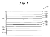
- FIG. 1 is a schematic cross-sectional view of a group III nitride semiconductor epitaxial substrate 100 according to an embodiment of the present invention.
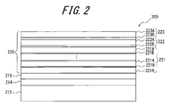
- 3 is a schematic cross-sectional view of a group III nitride semiconductor epitaxial substrate 200 according to a preferred embodiment of the present invention.
- FIG. FIG. 3 is an enlarged view of a first stacked body 221 in the group III nitride semiconductor epitaxial substrate 200 of FIG. 2.
- 3 is an example of a group III nitride semiconductor light emitting device 150 formed by providing element formation layer 130 on group III nitride semiconductor epitaxial substrate 100 according to an embodiment of the present invention.
- AlGaN when simply expressed as “AlGaN” in the present specification, the chemical composition ratio of the group III element (total of Al and Ga) and N is 1: 1, and the ratio of the group III element Al and Ga is 1: 1. Means an indeterminate arbitrary compound.
- the notation “AlGaN” does not exclude AlN or GaN.
- Al content when the ratio of the Al composition in the group III element in this compound does not change in the crystal growth direction, it is particularly referred to as “Al content”.
- the AlN layer and the surface portion in the present invention are both single crystal AlN layers, and are not AlN layers mainly composed of polycrystal or amorphous grown at a low temperature of 900 ° C. or lower, for example.
- a group III nitride semiconductor epitaxial substrate 100 includes a substrate 112 having at least a surface portion made of AlN, an undoped AlN layer 114 formed on the substrate 112, A Si-doped AlN buffer layer 116 formed on the undoped AlN layer 114 and a superlattice laminate 120 formed on the Si-doped AlN buffer layer 116 are included.
- the Si-doped AlN buffer layer 116 has a Si concentration of 2.0 ⁇ 10 19 / cm 3 or more and a thickness (also referred to as “film thickness”) of 4 to 10 nm. It is.
- the substrate 112 having at least a surface portion made of AlN includes an AlN template substrate in which an AlN single crystal is formed on a substrate made of a metal such as sapphire, SiC, Si, diamond, and Al, and an AlN single crystal in which the entire substrate is AlN. And a substrate.
- the thickness of the substrate 112 is appropriately set in consideration of the amount of warpage after epitaxial growth of each layer, and is in the range of 400 to 2000 ⁇ m, for example.
- AlN on the surface portion of the substrate 112 used in the present invention has good crystallinity.
- the half-value width of AlN on the (102) plane by X-ray rocking curve diffraction (XRC) is 600 seconds or less. It is preferable that it is a substrate.
- the dislocation density is preferably 1.0 ⁇ 10 9 / cm 2 or less. This is because by using a substrate with few dislocations, it is possible to suppress the occurrence of cracks due to excessive generation of dislocations when using the Si-doped AlN buffer layer 116 described later.
- An undoped AlN layer 114 is formed on the substrate 112 having at least a surface portion made of AlN.
- This undoped AlN layer 114 is intended to take over the crystallinity of AlN of a substrate with good crystallinity, and has a thickness in the range of 10 to 50 nm.
- “undoped” means that impurities are not intentionally doped, and does not intend to exclude unavoidable impurities due to the device or diffusion.
- the impurity concentration of impurities that can be p-type or n-type which are not inevitable impurities in undoping can be defined as 5.0 ⁇ 10 16 / cm 3 or less. This is a concentration that does not contribute to electrical conduction in a light emitting device such as an LED.
- a Si-doped AlN buffer layer 116 made of an AlN composition and having a Si concentration of 2.0 ⁇ 10 19 / cm 3 or more is formed.
- Si concentration means the value which carried out concentration conversion of the peak value of the detection intensity of the impurity obtained by SIMS (Secondary ion mass spectrometer: Secondary Ion-microprobe Mass Spectrometer).
- the thickness of the Si-doped AlN buffer layer 116 is 4 to 10 nm. The reason why the Si-doped AlN buffer layer 116 has a Si concentration of 2.0 ⁇ 10 19 / cm 3 or more and the reason for setting the thickness to 4 to 10 nm will be described later.
- a superlattice laminate 120 is formed on the Si-doped AlN buffer layer 116.
- the superlattice laminate 120 includes a first layer having a film thickness of about the de Broglie wavelength and a second layer having a composition different from that of the first layer and having a film thickness of about the de Broglie wavelength. It is formed by laminating a plurality of layers alternately. This superlattice laminate 120 can suppress dislocations to the outermost surface of the group III nitride semiconductor epitaxial substrate.
- the first Al-containing layer 120A is formed on the Si-doped AlN buffer layer 116, and the second Al-containing layer 120B and the first Al-containing layer 120A having different Al compositions are further stacked on the first Al-containing layer 120A.
- a lattice stack 120 can be formed.
- the lowermost layer and the uppermost layer of the superlattice laminate 120 are the first Al-containing layer 120A.
- the superlattice laminate 120 is not required to have conductivity, at least one of the first Al-containing layer 120A and the second Al-containing layer 120B is an undoped layer.
- one can be an undoped layer and the other can be a layer doped with impurities such as Mg.
- both the first Al-containing layer 120A and the second Al-containing layer 120B may be undoped.
- the first Al-containing layer 120A and the second Al-containing layer 120B can have AlGaN compositions having different average Al compositions.
- the Al content of the first Al-containing layer 120A can be made higher than the average composition of Al in the second Al-containing layer 120B.
- This superlattice laminate 120 is formed on the entire surface of the Si-doped AlN buffer layer 116.
- the group III nitride semiconductor according to one embodiment of the present invention has a Si concentration of 2.0 ⁇ 10 19 / cm 3 or more and a thickness of 4 to 10 nm. This is a particularly characteristic configuration of the epitaxial substrate 100. By adopting such a configuration, it is possible to provide a group III nitride semiconductor epitaxial substrate with better surface flatness.
- the present inventors have studied various buffer layers on the substrate 112 having at least a surface portion made of AlN.
- Si doping to the GaN layer Si doping to the AlN layer has been avoided in the past because a sharp uneven surface is generated on the surface of the AlN layer.
- the group 112 nitride semiconductor epitaxial substrate 100 excellent in surface flatness is obtained by the substrate 112, the undoped AlN layer 114, the Si-doped AlN layer 116, and the superlattice laminate 120.
- a buffer layer made of AlN (corresponding to the undoped AlN layer 114 and the Si-doped AlN buffer layer 116) is formed on the substrate 112, and the surface layer portion (Si-doped AlN buffer layer) on the side close to the superlattice laminate of the buffer layer. 116) (equivalent to 116) at a Si concentration of 2.0 ⁇ 10 19 / cm 3 or more, having a thickness of 4 nm or more, and further forming the superlattice laminate 120, the surface flatness was excellent. It has been found that a group III nitride semiconductor epitaxial substrate can be obtained.
- the group III nitride semiconductor The epitaxial substrate can have excellent surface flatness.
- the Si concentration is less than 2.0 ⁇ 10 19 / cm 3 , for example, 1.0 ⁇ 10 19 / cm 3
- the Si concentration of the Si-doped AlN buffer layer 116 is 2.0 ⁇ 10 19 / cm 3 or more, cracks due to the high-concentration Si doping may occur depending on the thickness of the Si-doped AlN buffer layer 116. It has also been found that the EL spectrum sometimes has a double peak.
- the Si-doped AlN buffer layer 116 has a Si concentration of 2.0 ⁇ 10 19 / cm 3 or more, if the thickness exceeds 10 nm, the Si-doped AlN buffer layer The amount of Si doping in the layer 116 as a whole becomes excessive, and the lattice relaxation tends to proceed so much that cracks tend to occur due to tensile strain. If the thickness is less than 4 nm, the Si-doped AlN buffer layer 116 as a whole lacks the amount of Si doping, so that defects generated on the Si-doped AlN buffer layer cannot be completely combined and disappear, and the EL spectrum shape has a double peak. It tends to become.
- the Si-doped AlN buffer layer 116 has a Si concentration of 2.0 ⁇ 10 19 / cm 3 or more, an element forming layer including a substrate 112 and a group III nitride layer grown on the Si-doped AlN buffer layer. It has also been found that the warpage of the group III nitride semiconductor epitaxial substrate can be reduced because of the effect of relaxing the strain between them.
- the undoped AlN layer 114 and the Si-doped AlN buffer layer 116 between the superlattice laminate 120 have a Si concentration of 2.0 ⁇ 10 19 / cm 3 or more, and the thickness thereof is 4 to 10 nm.
- the present inventors have found that the object of the present invention can be achieved, and the present invention has been completed.
- the group III nitride semiconductor epitaxial substrate according to the present invention can suppress the generation of cracks in the group III nitride semiconductor light emitting device using the same, and can make the EL spectrum normal single (one peak).
- Si doping to the buffer layer made of AlN has been conventionally avoided in order to obtain a semiconductor epitaxial substrate because it has the effect of forming irregularities on the surface of the buffer layer and roughening the surface.
- a substrate having many dislocations if used, a Si-doped AlN buffer layer is used, too many dislocations and cracks are considered to be a reason that has been conventionally avoided.
- a substrate with many dislocations there are many dislocations penetrating from the substrate, so there are many surface defect coalescence disappearances.
- the Si concentration is 2.0 ⁇ 10 19 / cm 3 or more, and by inserting a rather high concentration layer with an appropriate thickness, the surface defects are eliminated before the formation of the large convex portion, which is excellent. It has been found that surface flatness can be obtained and warpage can be further reduced.
- the group III nitride semiconductor epitaxial substrate 100 of the present embodiment can achieve excellent surface flatness by the above-described action. Even if a group III nitride semiconductor light emitting device is manufactured using the semiconductor epitaxial substrate 100, it is considered that generation of cracks can be suppressed and the EL spectrum shape can be made normal. Furthermore, the warp of the group III nitride semiconductor epitaxial substrate can be reduced.
- the superlattice laminate 220 is formed on the AlN buffer layer 216 with a high Al content in which the average composition x in the crystal growth direction is 0.9 ⁇ x ⁇ 1.
- a content layer Al x Ga 1-x N
- a low Al content layer Al y Ga 1-y N
- AlGaN layers are alternately stacked.
- the first to (n ⁇ 2) th low Al content layers counted from the AlN buffer layer side have the first thickness
- the (n ⁇ 1) th low Al content layer is the first thickness
- the nth low Al content layer has a third thickness that is equal to or greater than the second thickness.
- first laminated body 221 a laminate composed of layers from the high Al content layer immediately above the AlN buffer layer 216 to the (n-2) th high Al content layer counted from the AlN buffer layer 216 side is referred to as “ This is referred to as “first laminated body 221”.
- the high Al content layer in the first laminate 221 is represented as a high Al content layer 221A
- the low Al content layer is represented as a low Al content layer 221B
- the low Al-containing layer immediately above the first stacked body 221 is represented as a low Al-containing layer 222B
- the high Al-containing layer on the low Al-containing layer 222B is represented as a high Al-containing layer 222A.
- a laminate including the Al-containing layer 222A is referred to as a “second laminate 222”. Further, the low Al-containing layer immediately above the second stacked body 222 is represented as a low Al-containing layer 223B, and the high Al-containing layer on the low Al-containing layer 223B is represented as a high Al-containing layer 223A.
- a laminate including the Al-containing layer 223A is referred to as a “third laminate 223”. That is, the low Al content layer 222B is the (n ⁇ 1) th low Al content layer counted from the AlN buffer layer side and has the second thickness. The low Al content layer 223B is the nth low Al content layer counted from the AlN buffer layer side and has a third thickness.
- the superlattice laminate 220 On the AlN buffer layer 216, a superlattice laminate 220 composed of the first laminate 221, the second laminate 222, and the third laminate 223 described above is preferably formed.
- the superlattice laminate 220 includes a high Al content layer (Al x Ga 1-x N) having an average composition x in the crystal growth direction of 0.9 ⁇ x ⁇ 1, and an average in the crystal growth direction.
- composition y is 0 ⁇ y ⁇ low Al-containing layer consisting of x (Al y Ga 1-y N) preferably formed by laminating alternately two AlGaN layers of Al average composition of the.
- Al x Ga 1-x N (0.9 ⁇ x ⁇ 1) means that the Al composition is constant in the high Al content layer. Even if it exists, it may change continuously or discontinuously, and it means that the Al average composition x in the crystal growth direction is 0.9 ⁇ x ⁇ 1.
- Al average composition y of the low Al-containing layer is represented as “Al y Ga 1-y N (0 ⁇ y ⁇ x ⁇ 1)”.
- the high Al content layers 221A to 223A preferably have the same Al average composition x.
- the low Al-containing layers 221B to 223B preferably have the same Al average composition y.
- the number of superlattice stacks 220 the number of stacks of the low Al content layer and the high Al content layer that are alternately formed excluding the high Al content layer on the AlN buffer layer 216 is n sets (however, n is an integer satisfying 4 ⁇ n ⁇ 10).
- the first stacked body 221 has one high Al-containing layer 221A stacked on the AlN buffer layer 216, and the low Al-containing layer 221B and the high Al-containing layer 221A are alternately arranged in this order (n ⁇ 2) It is formed by stacking a set.
- the film thickness of the high Al-containing layer 221A can be about 1 to 10 nm.
- Each high Al content layer 221A in the first stacked body 221 can take any value within this range.
- the first thickness which is the thickness of the low Al-containing layer 221B, can be about 0.5 to 1.5 nm, but the first thickness can be constant in the first stacked body 221. preferable.
- the total film thickness of the first stacked body 221 can be about 3 to 92 nm.
- a low Al-containing layer 222B having a second thickness larger than the first thickness and a high Al-containing layer 222A are stacked one by one in this order.
- the film thickness of the high Al-containing layer 222A can be about 1 to 10 nm, and may be the same as or different from the film thickness of the high Al-containing layer 221A of the first stacked body 221.
- the film thickness (second thickness) of the low Al-containing layer 222B is 1.5 to 2 under the condition that the film thickness is larger than the first thickness of the low Al-containing layer 221B of the first stacked body 221. About 5 nm.
- the total film thickness of the second stacked body 222 can be about 2.5 to 12.5 nm.
- the 3rd laminated body 223 formed by laminating
- the film thickness of the high Al content layer 223A can be about 1 to 10 nm, and the film thickness of the high Al content layer 221A of the first stacked body 221 and / or the same film as the high Al content layer 222A of the second stacked body The thickness may be different or different.
- the film thickness (third thickness) of the low Al-containing layer 223B is equal to or greater than the film thickness (second thickness) of the low Al-containing layer 222B of the second stacked body 222, 1.5 ⁇ It can be about 3.5 nm.
- the second thickness and the third thickness may be the same, but as described later, More preferably, the thickness of 3 is greater than the second thickness.
- the upper limit of the number n of pairs in which the low Al content layer and the high Al content layer are alternately laminated is preferably 10 or less, and the occurrence position of defects is aligned by reducing the total thickness, Moreover, defects can be connected and eliminated, and as a result, planarization of the group III nitride semiconductor epitaxial substrate 200 can be promoted.
- the number of stacks of superlattice stack 220 is “6.5 sets”. That is, if the above-described n is used, the number of stacked groups of the superlattice stacked body 220 can be expressed as (n + 0.5) groups.
- the superlattice laminate 220 includes the first laminate 221, the second laminate 222, and the third laminate 223, and the number n of alternately stacked layers is preferably in the numerical range described above. Details will be described below.
- the inventors have changed the number of superlattice stacks 220 formed on the AlN buffer layer 216 to a conventionally known number of stacks (for example, Various studies were made on the surface flatness in the case of forming a considerably smaller number than 40.5).
- the impurity concentration of Si doping into the AlN buffer layer 216 is less than 2.0 ⁇ 10 19 / cm 3, the number of superlattice laminates 220 is 4.5, and the second and third laminates When not formed, irregularities with random heights were formed on the surface of the n-type contact layer formed on the superlattice laminate 220.
- the second and third stacked bodies are further provided without changing the impurity concentration to be doped with Si, and the number of superlattice stacked bodies 220 is 6.5, the superlattice stacked body 220 Although the surface of the n-type contact layer formed on the surface of the n-type contact layer was uneven, the height of the convex surface was uniform.
- the Si concentration of the Si-doped AlN buffer layer is set to 2.0 ⁇ 10 19 / cm 3 or more, the number of stacks of the first stack is 4.5, and the second and third stacks are superlattice stacked.
- the surface of the n-type contact layer formed on the superlattice laminate 220 has no irregularities and the height at the top surface is uniform when the number of laminated groups provided on the body 220 is 6.5. It was.
- Si doping to the buffer layer made of AlN has the effect of roughening the surface by forming irregularities on the surface of the buffer layer, so that a semiconductor epitaxial substrate having excellent surface flatness can be obtained.
- the present inventors have noted that by providing the second and third stacked bodies, only the uneven surface having the same height is formed on the uppermost surface of the superlattice stacked body 220. . Even if the number of stacks is 10.5 or less by increasing the saturation of the convex surfaces having the same height by doping Si in the AlN buffer layer 216 with a large amount, The present inventors have found that the flatness of the uppermost surface of the lattice laminate 220 is improved.
- the flatness of the uppermost surface of the superlattice laminate 220 is uniform because when only the first laminate was formed as the superlattice laminate 220, dislocations remained at random. This is because the formation of the second laminated body and the third laminated body having different thicknesses of the low Al-containing layer from the one laminated body leaves only dislocations in a certain direction, and the distortion is reduced by the formation of the surface defect.
- the inventors are thinking.
- the superlattice laminate 220 including the low Al-containing layers 221B to 223B having the first, second, and third thicknesses, a more excellent surface flatness and a reduced warpage are realized.
- a group III nitride semiconductor epitaxial substrate and a group III nitride semiconductor light emitting device can be obtained, which is preferable.
- the superlattice laminate 220 when n is 10 or less, the superlattice laminate 220 preferably includes both the second laminate 222 and the third laminate 223. This is because, when the number of laminated groups is considerably smaller than the conventionally known number of laminated groups (for example, 40.5 groups) (that is, when n is 10 or less), the first thickness of the low Al-containing layer 221B. This is because providing two or more low Al-containing layers having a large thickness facilitates dislocations only in a certain direction.
- the third thickness of the low Al-containing layer 223B is thicker than the second thickness of the low Al-containing layer 222B.
- the high Al content layers 221A to 223A preferably have the same thickness, so that a stress relaxation effect can be further obtained.
- the low Al-containing layers 221B to 223B made of Al y Ga 1-y N where the average composition in the crystal growth direction is 0 ⁇ y ⁇ x are composition gradient layers that reduce the Al composition along the crystal growth direction. It is preferable.
- a layer having an Al composition constant in the crystal growth direction with respect to the composition gradient layer is referred to as a “composition rectangular layer”.
- the low Al-containing layers 221B to 223B can obtain the effects of the present invention regardless of whether they are a composition gradient layer or a composition rectangular layer. However, for the following reasons, it is more preferable that the low Al-containing layers 221B to 223B are composition gradient layers.
- the composition gradient layer is a layer whose composition is inclined so that the Al composition in AlGaN decreases continuously or discontinuously in the crystal growth direction.
- the thermal expansion coefficient of the low Al-containing layer becomes a relatively high Al composition on the surface of the composition gradient layer on the substrate 212 side, and the expansion coefficient of the substrate. Get closer to.
- the surface of the gradient composition layer on the crystal growth direction side has a relatively low Al composition, and when the element formation layer is formed on the group III nitride semiconductor epitaxial substrate 210, it approaches the thermal expansion coefficient of the element formation layer. Therefore, the amount of warpage can be reduced and the occurrence of cracks can be suppressed.
- the value of the Al composition in AlGaN is y1 on the side close to the substrate 212 having at least a surface portion made of AlN and y2 on the surface near the substrate 212. Is in the range of 0.7 ⁇ y1 ⁇ x, more preferably in the range of 0.9 ⁇ y1 ⁇ x. On the surface in the crystal growth direction side, preferably in the range of 0 ⁇ y2 ⁇ 0.3. Yes, more preferably in the range of 0 ⁇ y2 ⁇ 0.1.
- the value of y is in the above range and the composition is tilted from y1 to y2, the difference in lattice constant between the substrate and the composition gradient layer is reduced, and as a result, the crystallinity when the element formation layer is formed can be improved. It is.
- the high Al content layer may be either a composition gradient layer or a composition rectangular layer, but a composition rectangular layer in which the Al composition is constant in the crystal growth direction is preferred.
- the Si concentration of the Si-doped AlN buffer layers 114 and 214 is 2.0 ⁇ 10 19 / cm 3 or more, the effect of the present invention can be obtained.
- the impurity concentration is more preferably less than 8 ⁇ 10 19 / cm 3 . This is because at 8 ⁇ 10 19 / cm 3 or more, the dislocation caused by the AlN buffer layer becomes excessive and cracks may occur.
- the group III nitride semiconductor epitaxial substrate 100 according to an embodiment of the present invention can be used for an arbitrary semiconductor element such as a light emitting element, a laser diode, or a transistor.
- FIG. 4 shows a group III nitride semiconductor light emitting device 150 formed using a group III nitride semiconductor epitaxial substrate 100 according to the present invention.
- the group III nitride semiconductor light emitting device 150 has an n-type cladding layer 133, an active layer 134, and a p-type cladding layer 135 in this order on the group III nitride semiconductor epitaxial substrate 100.
- a connection layer 131, an n-type contact layer 132, an n-type clad layer 133, and multiple layers as active layers are further formed on the superlattice laminate 120.
- An element formation layer 130 including a quantum well layer (MQW layer) 134, a p-type cladding layer 135, and a p-type contact layer 136 is sequentially formed.
- a part of the n-type contact layer 132 is exposed by, for example, dry etching, and the n-side electrode 141 and the p-type contact layer 136 are formed on the exposed n-type contact layer 132 and p-type contact layer 136.
- the group III nitride light-emitting element 150 having a lateral structure can be formed.
- the group III nitride semiconductor light emitting device 150 Since the group III nitride semiconductor light emitting device 150 has excellent surface flatness, the group III nitride semiconductor light emitting device 150 has high crystallinity, can suppress the occurrence of cracks, and the EL spectrum is Become normal.
- AlGaN constituting the high Al content layer and the low Al content layer may contain B and / or In which are other Group III elements in total of 1% or less. Further, for example, a trace amount of impurities such as Si, H, O, C, Mg, As, and P may be contained, and Mg impurities may be partially added intentionally. In addition, AlN constituting the group III nitride laminate may similarly contain other group III elements in total of 1% or less.
- the method for manufacturing a group III nitride semiconductor epitaxial substrate 100 of the present invention includes a step of forming an undoped AlN layer 114 on a substrate 112 having at least a surface portion made of AlN, and an AlN buffer layer 116 formed on the undoped AlN layer 114. And a step of forming a superlattice laminate 120 on the AlN buffer layer 116.
- Si doping is performed so that the Si concentration becomes 2.0 ⁇ 10 19 / cm 3 or more, and the thickness of the AlN buffer layer 116 is set to 4 to 10 nm.
- an n-type cladding layer 133, an active layer 134, and a p-type cladding layer 135 are further formed on the group III nitride semiconductor epitaxial substrate 100. And sequentially forming them.
- the superlattice laminate 220 described above may be formed instead of the superlattice laminate 120.
- a high Al-containing layer Al x Ga 1-x N having an average composition x in the crystal growth direction of 0.9 ⁇ x ⁇ 1 is laminated, and further in the crystal growth direction.
- the thickness of the low Al-containing layer from the first to the (n ⁇ 2) th from the AlN buffer layer 216 side is defined as the first thickness
- the (n ⁇ 1) th low Preferably, the thickness of the Al-containing layer is a second thickness that is greater than the first thickness
- the thickness of the nth low Al-containing layer is a third thickness that is equal to or greater than the second thickness.
- each layer in the present invention As a method for epitaxial growth of each layer in the present invention, a known method such as MOCVD method or MBE method can be used.
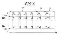
- source gases for forming AlGaN include TMA (trimethylaluminum), TMG (trimethylgallium), and ammonia.
- TMA trimethylaluminum
- TMG trimethylgallium
- ammonia ammonia
- each layer when the Al composition is constant as a composition rectangular layer, as shown in FIG. 5, the Al composition is changed by changing the mixing ratio of TMA and TMG with time according to the growth stage of each layer. Can be controlled. Moreover, if the epitaxial growth time is controlled, the film thickness of each layer can be arbitrarily controlled.
- the composition gradient layer can be formed by changing the mixing ratio of TMG and TMA over time according to the epitaxial growth time of each layer.
- an AlN layer (a high Al content layer) is formed with the TMA ratio being 100% without flowing TMG gas.
- the TMG gas starts to flow, and the TMG gas flow rate is changed from 0 sccm to the TMG flow rate at which the Al composition is theoretically 0.02 (Ga composition is 0.98) for a certain period of time.
- an AlGaN composition gradient layer (low Al-containing layer) in which the Al composition is continuously reduced from 1 to 0.02 in the crystal growth direction is formed (the average composition of Al is 0). .51).
- the TMG flow rate at which the Al composition becomes 0.02 means that a predetermined Al composition is obtained by flowing a predetermined TMA flow rate and a TMG flow rate under the crystal growth conditions of the apparatus to be used. Is the flow rate experimentally confirmed in advance. At this time, a layer having a sufficient thickness that enables quantitative analysis of the Al composition by SIMS may be formed, and the TMA flow rate and the TMG flow rate may be confirmed. In forming the composition gradient layer, the TMA gas flow rate is not necessarily constant, and may be changed according to the target Al composition.
- a stacked body (5 AlN layers and 4 AlGaN composition gradient layers) in which high Al-containing layers and low Al-containing layers are alternately stacked is formed as the first stacked body 221.
- the thicknesses (first thicknesses) of the low Al-containing layers are all equal if the epitaxial growth time is equal.
- an AlGaN composition gradient layer and an AlN layer as the second stacked body 222 are formed.
- the TMG flow rate is set to 0, and an AlN layer (high Al content layer) is formed.
- the thickness of the low Al-containing layer 222B in the second stacked body 222 is twice the film thickness (first thickness) of the low Al-containing layer 221B in the first stacked body 221.
- the rate of increase in the TMG flow rate per hour is further reduced as compared with the case of the second laminate, and the Al composition is increased while increasing the rate of increase in the TMG flow rate per hour correspondingly.
- the TMG flow rate is set to 0, and an AlN layer (high Al content layer) is formed.
- the film thickness of the low Al-containing layer 223B in the third stacked body 223 (third thickness) ) Is three times the film thickness (first thickness) of the low Al-containing layer 21 ⁇ / b> B in the first stacked body 221.
- the V / III ratio of ammonia to TMA and TMG may be determined as appropriate.
- Trial example 1 An AlN template substrate in which an undoped AlN layer (thickness: 600 nm, half width of AlN (102) plane by X-ray Rocking Curve): 242 seconds) is prepared on a sapphire substrate (thickness: 430 ⁇ m) is prepared did. After forming an undoped AlN layer having a thickness of 21.6 nm on this AlN template substrate by flowing TMA: 11.5 sccm and NH 3 : 575 sccm at a pressure of 10 kPa and a temperature of 1150 ° C.
- a Si-doped AlN buffer layer having a thickness of 5.4 nm doped with Si having an impurity concentration of 2.0 ⁇ 10 19 / cm 3 was formed by flowing 11.5 sccm, NH 3 : 575 sccm, and SiH 4 : 50 sccm. That is, an undoped AlN layer and a Si-doped AlN buffer layer are formed on the AlN template substrate. That is, the sum of the thicknesses of the undoped AlN layer and the Si-doped AlN buffer layer on the AlN template substrate is 27 nm, and the thickness doped with Si is 5.4 nm.
- the first stacked body, the second stacked body, and the third stacked body constituting the superlattice stacked body were sequentially epitaxially grown on the Si-doped AlN buffer layer.
- TMA 11.5 sccm
- NH 3 575 sccm were flowed for 300 seconds.
- a composition gradient layer having a film thickness of 1 nm and an average composition y 0.51 was used as the low Al-containing layer (Al y Ga 1-y N).
- the low Al-containing layer Al y Ga 1-y N
- TMA 11.5sccm
- NH 3 while flowing 575Sccm
- the low Al content layer is theoretically considered to have an Al composition continuously decreasing from 1 to 0.02 along the crystal growth direction.
- a high Al-containing layer was formed on the AlN buffer layer, and thereafter, four sets of low Al-containing layers and high Al-containing layers were alternately stacked.
- the first high Al-containing layer is counted as 0.5 pairs and becomes 4.5 pairs.
- the flow rate of TMG is the same as that of the first laminate except that the TMG flow rate is increased at a constant rate from 0 sccm to 45 sccm during the epitaxial growth time of 20 seconds.
- a third laminated body following the second laminated body a low Al content is obtained in the same manner as in the first laminated body except that the flow rate of TMG is increased at a constant rate from 0 sccm to 45 sccm during an epitaxial growth time of 30 seconds.
- an undoped AlGaN layer Al content: 0.7, thickness: 2400 nm
- an n-type AlGaN layer Al content: 0. 6 and a thickness of 1200 nm
- an n-type AlGaN layer Al content: 61%, film thickness: 1200 nm, dopant: Si
- an active layer AlGaN-based MQW layer, Film thickness: 74 nm, Al content of well layer: 41%
- p-type AlGaN layer as p-type cladding layer (Al content: 75%, film thickness: 20 nm, dopant: Mg)
- p-type GaN contact layer A flip-chip type group III nitride semiconductor light emitting device using the group III nitride epitaxial substrate of trial example 1 was fabricated by sequentially epitaxially growing film thickness: 35 nm, dopant: Mg).
- the group III nitride semiconductor light-emitting device according to Example 1 was manufactured as described above. In manufacturing the group III nitride semiconductor light-emitting device, a part of the n-type contact layer is exposed by dry etching, and an n-side electrode is formed on the exposed n-type contact layer and p-type contact layer. And the p-side electrode are arranged.
- the sum of the layer thicknesses of the undoped AlN layer and the Si-doped AlN buffer layer on the AlN template substrate is 27 nm.
- a test for changing the thickness of the AlN layer and the Si concentration is performed.
- Trial example 2 The group III nitride semiconductor epitaxial substrate and group III nitride according to Example 2 were manufactured in the same manner as in Example 1, except that the Si concentration of the Si-doped AlN buffer layer was changed to 4.0 ⁇ 10 19 / cm 3 . A semiconductor light emitting device was produced.
- Example 3 A Group III nitride semiconductor epitaxial substrate and Group III nitride according to Comparative Example 1 were produced in the same manner as in Example 1 except that the Si concentration of the Si-doped AlN buffer layer was changed to 1.2 ⁇ 10 19 / cm 3 . A semiconductor light emitting device was produced.
- Example 4 A Group III nitride semiconductor epitaxial substrate according to Example 3 was formed in the same manner as in Example 2 except that the undoped AlN layer was 18.9 nm and the thickness of the Si-doped AlN buffer layer was changed to 8.1 nm. A group III nitride semiconductor light emitting device was fabricated.
- Trial example 5 A Group III nitride semiconductor epitaxial substrate according to Comparative Example 2 and the Group III nitride semiconductor epitaxial substrate according to Comparative Example 2, except that the undoped AlN layer was 14.3 nm and the thickness of the Si-doped AlN buffer layer was changed to 2.7 nm. A group III nitride semiconductor light emitting device was fabricated.
- Trial Example 6 A Group III nitride semiconductor epitaxial substrate according to Comparative Example 3 was produced in the same manner as in Trial Example 1 except that the undoped AlN layer was not formed and the thickness of the Si-doped AlN buffer layer was changed to 27 nm.
- Trial Example 7 A Group III nitride semiconductor epitaxial substrate and Group III nitride according to Comparative Example 4 were formed in the same manner as in Trial Example 3, except that the undoped AlN layer was not formed and the thickness of the Si doped AlN buffer layer was changed to 27 nm. A semiconductor light emitting device was produced.
- the “warping amount” in the present invention means a value measured according to SEMI M1-0302. That is, the measurement is performed in a non-forced state, and the amount of warpage is the difference between the maximum value and the minimum value of all measurement point data in the non-adsorption state. As shown in FIG.
- the warpage is represented by the sum of the absolute value of the maximum value A and the minimum value B.
- the conventionally known group III nitride semiconductor epitaxial substrate has a thickness of about 140 ⁇ m. Therefore, a trial example with a warp amount of less than 100 ⁇ m was evaluated as “good”, and a trial example with a warp amount of 100 ⁇ m or more was evaluated as “x”.
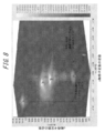
- mapping data was obtained.
- the measurement angle range of ⁇ was 31.5 ° to 35.7 ° at an interval of 0.01 °, and the measurement angle range of 2 ⁇ was 104.5 ° to 111.5 °.
- the part marked with “1” shows the peak of AlN
- the part marked with “2” shows the peak of the undoped AlGaN layer (connection layer)
- the portion marked “3” indicates the peak of the n-type AlGaN layer (n-type cladding layer). Note that the peak of the GaN composition appears at the site marked “9”.
- the light emission peak in the EL spectrum has one peak (convex portion) located at the peak wavelength assumed from the composition of the active layer (light emitting layer), and light is emitted even if there is a peak at other wavelengths. What is weak and negligible is referred to as “single”.
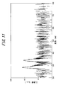
- the peak located at the peak wavelength assumed from the composition of the active layer (light emitting layer) the wavelength located 10 nm or more away from the peak wavelength, and the emission intensity cannot be ignored (for example, A case where two peaks with an intensity of 1/3 or more of the intensity of the assumed peak wavelength) is expressed as “double”.
- the EL spectra of the group III nitride semiconductor light emitting devices according to Trial Example 1 (Example 1) and Trial Example 5 (Comparative Example 2) are shown as representative examples in FIGS.
- the EL spectrum was single, and as shown in FIG. 10, one peak appeared at a peak wavelength of 285 nm assumed from the composition of the active layer.
- the EL spectrum was double, and as shown in FIG. 11, a peak at a wavelength of 339 nm appeared on the long wavelength side in addition to the peak at a wavelength of 285 nm.
- the light emission intensity is superior to the single light intensity than the double light intensity.
- the group III nitride semiconductor epitaxial substrates according to trial examples 1, 2, and 4 (that is, examples 1 to 3) that satisfy the conditions of the present invention had excellent surface flatness. Moreover, generation of cracks in the group III nitride semiconductor light-emitting device can be suppressed, and the EL spectrum shape is single. Furthermore, the group III nitride semiconductor epitaxial substrates according to trial examples 1, 2, and 4 showed a reduced amount of warpage as compared with conventionally known group III nitride semiconductor epitaxial substrates.
- the group III nitride semiconductor epitaxial substrate and the group III nitride semiconductor light emitting device according to trial examples 3, 5 to 7 (that is, comparative examples 1 to 4) that do not satisfy at least one of the conditions of the present invention have surface flatness. At least one condition among warp, crack, and EL spectrum could not be satisfied.
- the thickness of the Si-doped AlN layer needs to be 4 nm or more in order to realize excellent surface flatness. I understand that. Furthermore, comparing trial examples 1 and 6 in which only the thickness of the Si-doped AlN layer is different, the thickness of the Si-doped AlN layer needs to be 4 nm or more and 10 nm or less in order to suppress the occurrence of cracks. Recognize.
Landscapes
- Chemical & Material Sciences (AREA)
- Physics & Mathematics (AREA)
- Materials Engineering (AREA)
- Crystallography & Structural Chemistry (AREA)
- Metallurgy (AREA)
- Organic Chemistry (AREA)
- Engineering & Computer Science (AREA)
- Condensed Matter Physics & Semiconductors (AREA)
- General Physics & Mathematics (AREA)
- Electromagnetism (AREA)
- Optics & Photonics (AREA)
- Inorganic Chemistry (AREA)
- Led Devices (AREA)
- Semiconductor Lasers (AREA)
Abstract
Description
(1)少なくとも表面部分がAlNからなる基板と、該基板上に形成されるアンドープAlN層と、該アンドープAlN層上に形成されるSiドープAlNバッファ層と、該SiドープAlNバッファ層上に形成される超格子積層体と、を有するIII族窒化物半導体エピタキシャル基板において、
前記SiドープAlNバッファ層は、2.0×10¹⁹/cm3以上のSi濃度を有し、かつ、厚みが4~10nmであることを特徴とするIII族窒化物半導体エピタキシャル基板。
前記SiドープAlNバッファ層側から数えて1番目から(n−2)番目までの前記低Al含有層が、第1の厚みを有し、(n−1)番目の前記低Al含有層が、前記第1の厚みよりも厚い第2の厚みを有し、n番目の前記低Al含有層が、前記第2の厚み以上の第3の厚みを有する(1)に記載のIII族窒化物半導体エピタキシャル基板。
前記SiドープAlNバッファ層を形成する工程では、2.0×10¹⁹/cm3以上のSi濃度となるようにSiドープし、かつ、前記SiドープAlNバッファ層の厚みを4~10nmとすることを特徴とするIII族窒化物半導体エピタキシャル基板の製造方法。
なお、本発明に使用する基板112の表面部分のAlNは結晶性が良く、例えばX線ロッキングカーブ回折法(XRC;X−ray Rocking Curve)によるAlNの(102)面における半値幅が600秒以下の基板であることが好ましい。転位密度としては、1.0×10⁹/cm2以下であることが好ましい。転位の少ない基板を用いることで、後述するSiドープAlNバッファ層116を用いる場合の、転位発生が過剰になることによるクラック発生を抑制することができるためである。
転位が多い基板を使用した場合には、基板から貫通する転位が多いために面欠陥の合体消失も多く、そのため反って大きな凸が出来ず、結果的に平坦となる場合があった。一方、転位が少ない基板を使用した場合、基板から貫通する転位は僅かであり、面欠陥が発生しても、その面欠陥は消失せずに残り、大きな凸部を形成してしまうことが判明した。そこで、Si濃度を2.0×10¹⁹/cm3以上と、むしろ高濃度の層を適切な厚さで挿入することで、大きな凸部を形成する前に面欠陥を消失させて、優れた表面平坦性を得ることができると共に、さらに反りを低減できることを見出したのである。
AlNバッファ層216上には、既述の第1積層体221と、第2積層体222と、第3積層体223とから構成される超格子積層体220が形成されることが好ましい。この超格子積層体220は、既述のとおり、結晶成長方向の平均組成xが0.9<x≦1からなる高Al含有層(AlxGa1−xN)と、結晶成長方向の平均組成yが0<y<xからなる低Al含有層(AlyGa1−yN)との2種類のAl平均組成のAlGaN層を交互に積層してなることが好ましい。ここで、高Al含有層のAlの平均組成xに関し、「AlxGa1−xN(0.9<x≦1)」であるとは、Al組成が高Al含有層内において、一定であっても、連続的または不連続に変化してよく、結晶成長方向のAl平均組成xが0.9<x≦1であることを意味する。低Al含有層のAl平均組成yが「AlyGa1−yN(0<y<x≦1)」と表されることも、同様の意味である。また、高Al含有層221A~223Aは、同じAl平均組成xを有することが好ましい。同様に、低Al含有層221B~223Bは、同じAl平均組成yを有することが好ましい。
本発明者らは、III族窒化物半導体エピタキシャル基板200の反りをより低減するために、AlNバッファ層216上に形成する超格子積層体220の積層組数を、従来公知の積層組数(例えば、40.5組)よりも相当数減らして形成した場合の表面平坦性を種々検討した。AlNバッファ層216へのSiドープする不純物濃度を2.0×1019/cm3未満とし、超格子積層体220の積層組数が4.5組であり、かつ、第2および第3積層体を形成しなかった場合、超格子積層体220の上に形成されるn型コンタクト層の表面にはランダムな高さの凹凸が形成されていた。これに対して、Siドープする不純物濃度を変えずに、第2および第3積層体をさらに設けて超格子積層体220の積層組数を6.5組としたときに、超格子積層体220の上に形成されるn型コンタクト層の表面には、凹凸は発生するものの、その凸面の高さが揃っていた。これは、第2および第3積層体をさらに設けたことにより、同一面での核発生のみが残存したためだと考えられる。また、SiドープAlNバッファ層のSi濃度を2.0×1019/cm3以上とし、第1積層体の積層組数を4.5組として、さらに第2および第3積層体を超格子積層体220に設けて積層組数を6.5組としたときに、超格子積層体220の上に形成されるn型コンタクト層の表面には凹凸がなくなり、最上面での高さが揃っていた。これは、Siドープを多量とすることによって、面欠陥の発生源が増加して飽和し、その結果、同一面を発生起源とする面欠陥が成長方向に伸びる際に、ほぼ全ての隣り合う面欠陥同士が合体消滅したためであると本発明者らは考えている。
本発明のIII族窒化物半導体エピタキシャル基板100の製造方法は、少なくとも表面部分がAlNからなる基板112上にアンドープAlN層114を形成する工程と、該アンドープAlN層114上にAlNバッファ層116を形成する工程と、該AlNバッファ層116上に、超格子積層体120を形成する工程と、を有する。ここで、AlNバッファ層116を形成する工程では、2.0×10¹⁹/cm3以上のSi濃度となるようにSiドープし、かつ、AlNバッファ層116の厚みを4~10nmとすることを特徴とする。
サファイア基板(厚さ:430μm)上にアンドープのAlN層(厚さ:600nm、XRC(;X−ray Rocking Curve)によるAlN(102)面の半値幅:242秒)を形成したAlNテンプレート基板を用意した。このAlNテンプレート基板上に、MOCVD法を用いて、圧力10kPa、温度1150℃にてTMA:11.5sccm、NH3:575sccmを流して厚さ21.6nmのアンドープのAlN層を形成したのち、TMA:11.5sccm、NH3:575sccm、SiH4:50sccmを流して不純物濃度2.0×10¹⁹/cm3のSiがドープされた厚さ5.4nmのSiドープのAlNバッファ層を形成した。すなわち、AlNテンプレート基板上に、アンドープのAlN層と、SiドープされたAlNバッファ層が形成されている。すなわち、AlNテンプレート基板上の、アンドープのAlN層とSiドープされたAlNバッファ層の層厚の和は27nmであるうち、Siがドープされた厚さは5.4nmである。次に、SiドープされたAlNバッファ層上に、超格子積層体を構成する第1積層体、第2積層体および第3積層体を順次エピタキシャル成長させた。
SiドープAlNバッファ層のSi濃度を4.0×10¹⁹/cm3に変えた以外は、試行例1と同様の方法により、実施例2にかかるIII族窒化物半導体エピタキシャル基板およびIII族窒化物半導体発光素子を作製した。
SiドープAlNバッファ層のSi濃度を1.2×10¹⁹/cm3に変えた以外は、試行例1と同様の方法により、比較例1にかかるIII族窒化物半導体エピタキシャル基板およびIII族窒化物半導体発光素子を作製した。
アンドープのAlN層を18.9nmとし、SiドープAlNバッファ層の膜厚を8.1nmに変えた以外は、試行例2と同様の方法により、実施例3にかかるIII族窒化物半導体エピタキシャル基板およびIII族窒化物半導体発光素子を作製した。
アンドープのAlN層を14.3nmとし、SiドープAlNバッファ層の膜厚を2.7nmに変えた以外は、試行例2と同様の方法により、比較例2にかかるIII族窒化物半導体エピタキシャル基板およびIII族窒化物半導体発光素子を作製した。
アンドープのAlN層を形成せず、SiドープAlNバッファ層の膜厚を27nmに変えた以外は、試行例1と同様の方法により、比較例3にかかるIII族窒化物半導体エピタキシャル基板を作製した。
アンドープのAlN層を形成せず、SiドープAlNバッファ層の膜厚を27nmに変えた以外は、試行例3と同様の方法により、比較例4にかかるIII族窒化物半導体エピタキシャル基板およびIII族窒化物半導体発光素子を作製した。

各試行例のIII族窒化物半導体エピタキシャル基板について、金属顕微鏡装置(Nikon社製)を用い、n型コンタクト層表面の表面写真を取得し、表面凹凸の有無を判定した。表面凹凸がなければ、III族窒化物半導体エピタキシャル基板の表面平坦性が優れていることを意味する。結果を表1に示す。なお、表1中、表面凹凸があったものを×とし、表面凹凸がなかったものを○と評価している。
各試行例のIII族窒化物半導体エピタキシャル基板について、光学干渉方式による反り測定装置(Nidek社製、FT−900)を用いて、超格子積層体上の、中間層およびn型コンタクト層の形成後の基板の反り量をSEMI規格に準じて測定した。結果を表1に示す。本発明における「反り量」は、SEMI M1−0302に準じて測定したものを意味するものとする。すなわち、非強制状態で測定を行い、反り量は非吸着での全測定点データの最大値と最小値との差の値である。図7に示すように、基準面を最小二乗法により求められた仮想平面とすると、反り量(SORI)は最大値Aと最小値Bの絶対値の和で示される。なお、従来公知のIII族窒化物半導体エピタキシャル基板は140μm程度である。そこで、反り量が100μm未満の試行例を○と評価し、100μm以上である試行例を×と評価した。
各試行例のIII族窒化物半導体発光素子について、金属顕微鏡(Nikon社製)を用い、素子表面の表面写真を取得し、表面凹凸の有無に加えて、クラック発生の有無を判定した。結果を表1に示す。なお、表1中、クラックの発生について、下記のとおり評価した。
◎:クラックの発生が表面写真では確認できない。
○:クラックの発生が表面写真では一部確認できるが、実用上許容できる。
×:クラックが明確に発生しており、許容できない。
ここで、基板外周から5mm以内にあるクラック、および、基板外周から5mmより内側にあるクラックであって直線の本数が5本以内である場合に、実用上許容できるクラックと判定する。
試行例1(実施例1)にかかるIII族窒化物半導体発光素子では、図8に示されるように、格子定数が回復して、n型AlGaN層(「3」の部位)のピークがAlGaNのラインに近づき、引っ張り歪み量が低減する結果、n型AlGaN層(n型クラッド層)でのクラック発生が抑制されると考えられる。一方、図9からわかるように、試行例6(比較例3)にかかるIII族窒化物半導体発光素子では、n型AlGaN層(「3」の部位)のピークがAlGaNのラインから大きく外れる。このことは、a軸が伸び、c軸が縮むために、引っ張り歪み量が増加したからだと考えられ、n型クラッド層でのクラック発生の原因となる。
各試行例のIII族窒化物半導体発光素子について、結晶成長面をダイヤペンで罫書き、n型クラッド層(n型AlGaN層)を露出させた点と、この露出させた点から1.5mm離れた点とに、ドット状のインジウムを物理的に押圧して2点を成形した。そして、この2点をそれぞれn型およびp型電極とする簡易的な窒化物半導体素子を作製した。この発光素子の電極にプローバーを接触させ、直流電流10mAを通電した後の光出力を基板の裏面より射出させ、光ファイバを通じてマルチ・チャンネル型分光器へ導光し、ELスペクトルを測定した。結果を表1に示す。表1中、ELスペクトルにおける発光ピークが、活性層(発光層)の組成から想定されるピーク波長に位置するピーク(凸部)が1つであり、他の波長にピークがあったとしても発光強度が弱く、無視できるほどであったものを「シングル」と表記する。また、発光ピークのスペクトルにおいて、活性層(発光層)の組成から想定されるピーク波長に位置するピークと、そのピーク波長から10nm以上離れた波長に位置にし、かつ発光強度が無視できない程度(例えば想定されるピーク波長の強度の1/3以上)のピークとの2つが現れたものを「ダブル」と表記する。ここで、試行例1(実施例1),試行例5(比較例2)にかかるIII族窒化物半導体発光素子のELスペクトルを、代表例として図10,図11にそれぞれ示す。試行例1(実施例1)ではELスペクトルがシングルであり、図10に示すように、活性層の組成から想定されるピーク波長285nmにピークが1つ現れた。一方、試行例5(比較例2)ではELスペクトルがダブルであり、図11に示すように、波長285nmのピークの他に、長波長側に波長339nmのピークが現れた。なお、発光強度については、図10および図11から明らかなように、シングルの方がダブルの場合よりも強度が優れる。
SiドープAlN層のSi濃度のみが異なる試行例1~3を比較すると、Si濃度が2.0×10¹⁹/cm3未満であると、ELスペクトルのピークがダブルになっていた。また、試行例1~3とは厚みは異なるが、やはりSiドープAlN層のSi濃度のみが異なる試行例6,7を比較しても、Si濃度が2.0×1019/cm3未満であると、ELスペクトルのピークがダブルになっていた。したがって、Si濃度が2.0×1019/cm3未満であると、ELスペクトルのピークがダブルになってしまう傾向にあることがわかる。
112,212 基板(少なくとも表面部分がAlNからなる基板)
114,214 アンドープAlN層
116,216 SiドープAlNバッファ層
120,220 超格子積層体
120A 第1Al含有層
120B 第2Al含有層
130 素子形成層
131 接続層
132 n型コンタクト層
133 n型クラッド層
134 多重量子井戸層(MQW層)
135 p型クラッド層
136 p型コンタクト層
141 n側電極
142 p側電極
150 III族窒化物半導体発光素子
221 第1積層体
221A 高Al含有層(AlxGa1−xN)
221B 低Al含有層(AlyGa1−yN)
222 第2積層体
222A 高Al含有層(AlxGa1−xN)
222B 低Al含有層(AlyGa1−yN)
223 第3積層体
223A 高Al含有層(AlxGa1−xN)
223B 低Al含有層(AlyGa1−yN)
Claims (9)
- 少なくとも表面部分がAlNからなる基板と、
該基板上に形成されるアンドープAlN層と、
該アンドープAlN層上に形成されるSiドープAlNバッファ層と、
該SiドープAlNバッファ層上に形成される超格子積層体と、を有するIII族窒化物半導体エピタキシャル基板において、
前記SiドープAlNバッファ層は、2.0×10¹⁹/cm3以上のSi濃度を有し、かつ、厚みが4~10nmであることを特徴とするIII族窒化物半導体エピタキシャル基板。 - 前記超格子積層体は、前記SiドープAlNバッファ層上に、結晶成長方向の平均組成xが0.9<x≦1からなる高Al含有層(AlxGa1−xN)を積層し、さらに結晶成長方向の平均組成yが0<y<xからなる低Al含有層(AlyGa1−yN)と前記高Al含有層とを交互にn組(但し、nは4≦n≦10を満たす整数である)積層してなり、
前記SiドープAlNバッファ層側から数えて1番目から(n−2)番目までの前記低Al含有層が、第1の厚みを有し、(n−1)番目の前記低Al含有層が、前記第1の厚みよりも厚い第2の厚みを有し、n番目の前記低Al含有層が、前記第2の厚み以上の第3の厚みを有する請求項1に記載のIII族窒化物半導体エピタキシャル基板。 - 前記低Al含有層は、Al組成が結晶成長方向に沿って減少する組成傾斜層である請求項2に記載のIII族窒化物半導体エピタキシャル基板。
- 前記高Al含有層は、AlN層(x=1)である請求項2または3に記載のIII族窒化物半導体エピタキシャル基板。
- 前記第3の厚みは、前記第2の厚みよりも厚い請求項2~4いずれか1項に記載のIII族窒化物半導体エピタキシャル基板。
- 前記高Al含有層は、等しい厚みを有する請求項2~5いずれか1項に記載のIII族窒化物半導体エピタキシャル基板。
- 請求項1~6いずれか1項に記載のIII族窒化物半導体エピタキシャル基板と、該基板上にn型クラッド層と、活性層と、p型クラッド層とをこの順に有するIII族窒化物半導体発光素子。
- 少なくとも表面部分がAlNからなる基板上にアンドープAlN層を形成する工程と、
該アンドープAlN層上にSiドープAlNバッファ層を形成する工程と、
該SiドープAlNバッファ層上に超格子積層体を形成する工程と、とを有するIII族窒化物半導体エピタキシャル基板の製造方法において、
前記SiドープAlNバッファ層を形成する工程では、2.0×10¹⁹/cm3以上のSi濃度となるようにSiドープし、かつ、前記SiドープAlNバッファ層の厚みを4~10nmとすることを特徴とするIII族窒化物半導体エピタキシャル基板の製造方法。 - 請求項8に記載のIII族窒化物半導体エピタキシャル基板上に、さらにn型クラッド層と、活性層と、p型クラッド層とを順次形成する工程とを有するIII族窒化物半導体発光素子の製造方法。
Priority Applications (2)
| Application Number | Priority Date | Filing Date | Title |
|---|---|---|---|
| US14/904,207 US9543469B2 (en) | 2013-08-09 | 2014-08-06 | III nitride semiconductor epitaxial substrate and III nitride semiconductor light emitting device, and methods of producing the same |
| CN201480044414.2A CN105493241B (zh) | 2013-08-09 | 2014-08-06 | 第iii族氮化物半导体外延基板和第iii族氮化物半导体发光元件以及它们的制造方法 |
Applications Claiming Priority (2)
| Application Number | Priority Date | Filing Date | Title |
|---|---|---|---|
| JP2013166377A JP5698321B2 (ja) | 2013-08-09 | 2013-08-09 | Iii族窒化物半導体エピタキシャル基板およびiii族窒化物半導体発光素子ならびにこれらの製造方法 |
| JP2013-166377 | 2013-08-09 |
Publications (1)
| Publication Number | Publication Date |
|---|---|
| WO2015020233A1 true WO2015020233A1 (ja) | 2015-02-12 |
Family
ID=52461552
Family Applications (1)
| Application Number | Title | Priority Date | Filing Date |
|---|---|---|---|
| PCT/JP2014/071351 Ceased WO2015020233A1 (ja) | 2013-08-09 | 2014-08-06 | Iii族窒化物半導体エピタキシャル基板およびiii族窒化物半導体発光素子ならびにこれらの製造方法 |
Country Status (4)
| Country | Link |
|---|---|
| US (1) | US9543469B2 (ja) |
| JP (1) | JP5698321B2 (ja) |
| CN (1) | CN105493241B (ja) |
| WO (1) | WO2015020233A1 (ja) |
Cited By (4)
| Publication number | Priority date | Publication date | Assignee | Title |
|---|---|---|---|---|
| CN107278333A (zh) * | 2015-02-25 | 2017-10-20 | Lg 伊诺特有限公司 | 发光器件和具有发光器件的灯单元 |
| CN109075226A (zh) * | 2016-04-27 | 2018-12-21 | 斯坦雷电气株式会社 | Iii族氮化物层叠体及iii族氮化物发光元件 |
| CN114256057A (zh) * | 2020-09-25 | 2022-03-29 | 华为技术有限公司 | 氮化物外延结构和半导体器件 |
| US20220406959A1 (en) * | 2021-06-22 | 2022-12-22 | Samsung Electronics Co., Ltd. | Nanorod light emitting device, substrate structure including a plurality of nanorod light emitting devices, and method of manufacturing the substrate structure |
Families Citing this family (16)
| Publication number | Priority date | Publication date | Assignee | Title |
|---|---|---|---|---|
| JP5698321B2 (ja) * | 2013-08-09 | 2015-04-08 | Dowaエレクトロニクス株式会社 | Iii族窒化物半導体エピタキシャル基板およびiii族窒化物半導体発光素子ならびにこれらの製造方法 |
| TWI577046B (zh) * | 2014-12-23 | 2017-04-01 | 錼創科技股份有限公司 | 半導體發光元件及其製作方法 |
| CN105374912B (zh) * | 2015-10-28 | 2017-11-21 | 厦门市三安光电科技有限公司 | 发光二极管及其制作方法 |
| US10586701B2 (en) * | 2016-02-26 | 2020-03-10 | Sanken Electric Co., Ltd. | Semiconductor base having a composition graded buffer layer stack |
| JP6268229B2 (ja) * | 2016-06-27 | 2018-01-24 | 株式会社サイオクス | 窒化物半導体積層物、窒化物半導体積層物の製造方法、半導体積層物の製造方法、および半導体積層物の検査方法 |
| US9680056B1 (en) * | 2016-07-08 | 2017-06-13 | Bolb Inc. | Ultraviolet light-emitting device with a heavily doped strain-management interlayer |
| JP6993843B2 (ja) * | 2017-10-27 | 2022-01-14 | 日機装株式会社 | 窒化物半導体発光素子及び窒化物半導体発光素子の製造方法 |
| KR102374879B1 (ko) * | 2017-12-19 | 2022-03-15 | 가부시키가이샤 사무코 | Ⅲ족 질화물 반도체 기판의 제조 방법 |
| CN109638121B (zh) * | 2018-12-19 | 2020-01-31 | 湘能华磊光电股份有限公司 | 4英寸led外延生长方法 |
| JP7338166B2 (ja) * | 2019-02-25 | 2023-09-05 | 日本電信電話株式会社 | 半導体装置 |
| JP2020177965A (ja) * | 2019-04-16 | 2020-10-29 | 日機装株式会社 | 窒化物半導体発光素子 |
| US12419142B2 (en) * | 2020-09-17 | 2025-09-16 | Nikkiso Co., Ltd. | Nitride semiconductor ultraviolet light emitting element |
| CN112242460A (zh) * | 2020-09-29 | 2021-01-19 | 苏州紫灿科技有限公司 | 一种具有Si掺杂插入层的AlN复合薄膜及其外延生长方法 |
| JP7368336B2 (ja) * | 2020-09-30 | 2023-10-24 | 信越半導体株式会社 | 紫外線発光素子用金属貼り合わせ基板の製造方法、及び紫外線発光素子の製造方法 |
| CN114725259B (zh) * | 2022-04-08 | 2026-03-20 | 江西兆驰半导体有限公司 | 发光二极管外延片及其外延生长方法、发光二极管芯片 |
| CN121586397B (zh) * | 2026-01-28 | 2026-04-07 | 材料科学姑苏实验室 | 氧化镓外延片及其制备方法、日盲紫外光电探测器 |
Citations (6)
| Publication number | Priority date | Publication date | Assignee | Title |
|---|---|---|---|---|
| JP2008539587A (ja) * | 2005-04-29 | 2008-11-13 | クリー インコーポレイテッド | 2元のiii族窒化物をベースとする高電子移動度トランジスタおよびその製造方法 |
| WO2011102045A1 (ja) * | 2010-02-16 | 2011-08-25 | 日本碍子株式会社 | エピタキシャル基板およびエピタキシャル基板の製造方法 |
| JP2011205053A (ja) * | 2009-08-24 | 2011-10-13 | Dowa Electronics Materials Co Ltd | 窒化物半導体素子およびその製造方法 |
| JP2012089871A (ja) * | 2001-12-03 | 2012-05-10 | Cree Inc | へテロ接合トランジスタ及びその製造方法 |
| EP2615650A2 (en) * | 2012-01-13 | 2013-07-17 | DOWA Electronics Materials Co., Ltd. | III-nitride epitaxial substrate and deep ultraviolet light emiting device using the same |
| WO2013125126A1 (ja) * | 2012-02-23 | 2013-08-29 | 日本碍子株式会社 | 半導体素子および半導体素子の製造方法 |
Family Cites Families (6)
| Publication number | Priority date | Publication date | Assignee | Title |
|---|---|---|---|---|
| JP2004047764A (ja) | 2002-07-12 | 2004-02-12 | Hitachi Cable Ltd | 窒化物半導体の製造方法および半導体ウェハならびに半導体デバイス |
| WO2008020599A1 (fr) * | 2006-08-18 | 2008-02-21 | Showa Denko K.K. | Procédé de fabrication d'un dispositif électroluminescent comportant un semi-conducteur formé d'un nitrure du groupe iii, dispositif électroluminescent correspondant et lampe |
| JP4644754B2 (ja) * | 2008-03-13 | 2011-03-02 | 昭和電工株式会社 | Iii族窒化物半導体素子及びiii族窒化物半導体発光素子 |
| TWI413279B (zh) * | 2008-06-20 | 2013-10-21 | 豐田合成股份有限公司 | Iii族氮化物半導體發光元件及其製造方法、以及燈 |
| KR20140010587A (ko) * | 2012-07-13 | 2014-01-27 | 삼성전자주식회사 | 도핑된 버퍼층을 포함하는 반도체 발광 소자 및 그 제조 방법 |
| JP5698321B2 (ja) * | 2013-08-09 | 2015-04-08 | Dowaエレクトロニクス株式会社 | Iii族窒化物半導体エピタキシャル基板およびiii族窒化物半導体発光素子ならびにこれらの製造方法 |
-
2013
- 2013-08-09 JP JP2013166377A patent/JP5698321B2/ja active Active
-
2014
- 2014-08-06 CN CN201480044414.2A patent/CN105493241B/zh active Active
- 2014-08-06 US US14/904,207 patent/US9543469B2/en active Active
- 2014-08-06 WO PCT/JP2014/071351 patent/WO2015020233A1/ja not_active Ceased
Patent Citations (6)
| Publication number | Priority date | Publication date | Assignee | Title |
|---|---|---|---|---|
| JP2012089871A (ja) * | 2001-12-03 | 2012-05-10 | Cree Inc | へテロ接合トランジスタ及びその製造方法 |
| JP2008539587A (ja) * | 2005-04-29 | 2008-11-13 | クリー インコーポレイテッド | 2元のiii族窒化物をベースとする高電子移動度トランジスタおよびその製造方法 |
| JP2011205053A (ja) * | 2009-08-24 | 2011-10-13 | Dowa Electronics Materials Co Ltd | 窒化物半導体素子およびその製造方法 |
| WO2011102045A1 (ja) * | 2010-02-16 | 2011-08-25 | 日本碍子株式会社 | エピタキシャル基板およびエピタキシャル基板の製造方法 |
| EP2615650A2 (en) * | 2012-01-13 | 2013-07-17 | DOWA Electronics Materials Co., Ltd. | III-nitride epitaxial substrate and deep ultraviolet light emiting device using the same |
| WO2013125126A1 (ja) * | 2012-02-23 | 2013-08-29 | 日本碍子株式会社 | 半導体素子および半導体素子の製造方法 |
Cited By (6)
| Publication number | Priority date | Publication date | Assignee | Title |
|---|---|---|---|---|
| CN107278333A (zh) * | 2015-02-25 | 2017-10-20 | Lg 伊诺特有限公司 | 发光器件和具有发光器件的灯单元 |
| US10381509B2 (en) | 2015-02-25 | 2019-08-13 | Lg Innotek Co., Ltd. | Light emitting device and light unit having same |
| CN109075226A (zh) * | 2016-04-27 | 2018-12-21 | 斯坦雷电气株式会社 | Iii族氮化物层叠体及iii族氮化物发光元件 |
| CN114256057A (zh) * | 2020-09-25 | 2022-03-29 | 华为技术有限公司 | 氮化物外延结构和半导体器件 |
| US20220406959A1 (en) * | 2021-06-22 | 2022-12-22 | Samsung Electronics Co., Ltd. | Nanorod light emitting device, substrate structure including a plurality of nanorod light emitting devices, and method of manufacturing the substrate structure |
| US12249671B2 (en) * | 2021-06-22 | 2025-03-11 | Samsung Electronics Co., Ltd. | Nanorod light emitting device, substrate structure including a plurality of nanorod light emitting devices, and method of manufacturing the substrate structure |
Also Published As
| Publication number | Publication date |
|---|---|
| US9543469B2 (en) | 2017-01-10 |
| CN105493241B (zh) | 2017-10-24 |
| US20160172534A1 (en) | 2016-06-16 |
| JP5698321B2 (ja) | 2015-04-08 |
| JP2015035536A (ja) | 2015-02-19 |
| CN105493241A (zh) | 2016-04-13 |
Similar Documents
| Publication | Publication Date | Title |
|---|---|---|
| JP5698321B2 (ja) | Iii族窒化物半導体エピタキシャル基板およびiii族窒化物半導体発光素子ならびにこれらの製造方法 | |
| JP6226627B2 (ja) | Iii族窒化物半導体エピタキシャル基板およびその製造方法 | |
| JP5514920B2 (ja) | Iii族窒化物エピタキシャル基板および該基板を用いた深紫外発光素子 | |
| JP5521068B1 (ja) | Iii族窒化物半導体発光素子 | |
| US8759851B2 (en) | Nitride semiconductor device, nitride semiconductor wafer and method for manufacturing nitride semiconductor layer | |
| JP6302254B2 (ja) | 窒化物半導体素子、窒化物半導体ウェーハ、及び、窒化物半導体素子の製造方法 | |
| US20140084338A1 (en) | Semiconductor wafer, semiconductor device, and method for manufacturing nitride semiconductor layer | |
| JP2013014450A (ja) | 窒化物半導体エピタキシャル基板及び窒化物半導体デバイス | |
| JP6033342B2 (ja) | Iii族窒化物半導体発光素子およびその製造方法 | |
| CN102790155B (zh) | 氮化物半导体器件和晶片以及制造氮化物半导体层的方法 | |
| CN106784181B (zh) | 提高绿光或更长波长InGaN量子阱发光效率的方法及结构 | |
| JP3976723B2 (ja) | 半導体素子およびその製造方法 | |
| JP5865271B2 (ja) | 結晶積層構造体及び発光素子 | |
| JP5327778B2 (ja) | 半導体素子およびその製造方法 | |
| JP7205474B2 (ja) | テンプレート基板、電子デバイス,発光デバイス,テンプレート基板の製造方法および電子デバイスの製造方法 | |
| JP5175967B1 (ja) | 半導体発光素子及び半導体ウェーハ | |
| JP6071044B2 (ja) | 半導体発光素子及びその製造方法 | |
| KR101850537B1 (ko) | 반도체 소자 | |
| JP2008034754A (ja) | 発光素子 | |
| JP2014146684A (ja) | 半導体発光素子及びその製造方法 | |
| JP2013084957A (ja) | 半導体発光素子 | |
| KR20120128088A (ko) | 질화물 반도체 소자, 질화물 반도체 웨이퍼 및 질화물 반도체층의 제조 방법 |
Legal Events
| Date | Code | Title | Description |
|---|---|---|---|
| WWE | Wipo information: entry into national phase |
Ref document number: 201480044414.2 Country of ref document: CN |
|
| 121 | Ep: the epo has been informed by wipo that ep was designated in this application |
Ref document number: 14835270 Country of ref document: EP Kind code of ref document: A1 |
|
| WWE | Wipo information: entry into national phase |
Ref document number: 14904207 Country of ref document: US |
|
| NENP | Non-entry into the national phase |
Ref country code: DE |
|
| 122 | Ep: pct application non-entry in european phase |
Ref document number: 14835270 Country of ref document: EP Kind code of ref document: A1 |