WO2015016107A1 - 光電変換素子および太陽電池 - Google Patents
光電変換素子および太陽電池 Download PDFInfo
- Publication number
- WO2015016107A1 WO2015016107A1 PCT/JP2014/069404 JP2014069404W WO2015016107A1 WO 2015016107 A1 WO2015016107 A1 WO 2015016107A1 JP 2014069404 W JP2014069404 W JP 2014069404W WO 2015016107 A1 WO2015016107 A1 WO 2015016107A1
- Authority
- WO
- WIPO (PCT)
- Prior art keywords
- group
- photoelectric conversion
- formula
- conversion element
- substituent
- Prior art date
- Legal status (The legal status is an assumption and is not a legal conclusion. Google has not performed a legal analysis and makes no representation as to the accuracy of the status listed.)
- Ceased
Links
Images



Classifications
-
- H—ELECTRICITY
- H10—SEMICONDUCTOR DEVICES; ELECTRIC SOLID-STATE DEVICES NOT OTHERWISE PROVIDED FOR
- H10K—ORGANIC ELECTRIC SOLID-STATE DEVICES
- H10K85/00—Organic materials used in the body or electrodes of devices covered by this subclass
- H10K85/60—Organic compounds having low molecular weight
- H10K85/631—Amine compounds having at least two aryl rest on at least one amine-nitrogen atom, e.g. triphenylamine
- H10K85/633—Amine compounds having at least two aryl rest on at least one amine-nitrogen atom, e.g. triphenylamine comprising polycyclic condensed aromatic hydrocarbons as substituents on the nitrogen atom
-
- H—ELECTRICITY
- H10—SEMICONDUCTOR DEVICES; ELECTRIC SOLID-STATE DEVICES NOT OTHERWISE PROVIDED FOR
- H10F—INORGANIC SEMICONDUCTOR DEVICES SENSITIVE TO INFRARED RADIATION, LIGHT, ELECTROMAGNETIC RADIATION OF SHORTER WAVELENGTH OR CORPUSCULAR RADIATION
- H10F77/00—Constructional details of devices covered by this subclass
- H10F77/10—Semiconductor bodies
- H10F77/12—Active materials
- H10F77/127—Active materials comprising only Group IV-VI or only Group II-IV-VI chalcogenide materials, e.g. PbSnTe
-
- H—ELECTRICITY
- H10—SEMICONDUCTOR DEVICES; ELECTRIC SOLID-STATE DEVICES NOT OTHERWISE PROVIDED FOR
- H10K—ORGANIC ELECTRIC SOLID-STATE DEVICES
- H10K85/00—Organic materials used in the body or electrodes of devices covered by this subclass
-
- H—ELECTRICITY
- H10—SEMICONDUCTOR DEVICES; ELECTRIC SOLID-STATE DEVICES NOT OTHERWISE PROVIDED FOR
- H10K—ORGANIC ELECTRIC SOLID-STATE DEVICES
- H10K85/00—Organic materials used in the body or electrodes of devices covered by this subclass
- H10K85/50—Organic perovskites; Hybrid organic-inorganic perovskites [HOIP], e.g. CH3NH3PbI3
-
- H—ELECTRICITY
- H10—SEMICONDUCTOR DEVICES; ELECTRIC SOLID-STATE DEVICES NOT OTHERWISE PROVIDED FOR
- H10K—ORGANIC ELECTRIC SOLID-STATE DEVICES
- H10K85/00—Organic materials used in the body or electrodes of devices covered by this subclass
- H10K85/60—Organic compounds having low molecular weight
- H10K85/631—Amine compounds having at least two aryl rest on at least one amine-nitrogen atom, e.g. triphenylamine
-
- H—ELECTRICITY
- H10—SEMICONDUCTOR DEVICES; ELECTRIC SOLID-STATE DEVICES NOT OTHERWISE PROVIDED FOR
- H10K—ORGANIC ELECTRIC SOLID-STATE DEVICES
- H10K85/00—Organic materials used in the body or electrodes of devices covered by this subclass
- H10K85/60—Organic compounds having low molecular weight
- H10K85/631—Amine compounds having at least two aryl rest on at least one amine-nitrogen atom, e.g. triphenylamine
- H10K85/636—Amine compounds having at least two aryl rest on at least one amine-nitrogen atom, e.g. triphenylamine comprising heteroaromatic hydrocarbons as substituents on the nitrogen atom
-
- H—ELECTRICITY
- H10—SEMICONDUCTOR DEVICES; ELECTRIC SOLID-STATE DEVICES NOT OTHERWISE PROVIDED FOR
- H10K—ORGANIC ELECTRIC SOLID-STATE DEVICES
- H10K85/00—Organic materials used in the body or electrodes of devices covered by this subclass
- H10K85/60—Organic compounds having low molecular weight
- H10K85/649—Aromatic compounds comprising a hetero atom
- H10K85/654—Aromatic compounds comprising a hetero atom comprising only nitrogen as heteroatom
-
- H—ELECTRICITY
- H10—SEMICONDUCTOR DEVICES; ELECTRIC SOLID-STATE DEVICES NOT OTHERWISE PROVIDED FOR
- H10K—ORGANIC ELECTRIC SOLID-STATE DEVICES
- H10K30/00—Organic devices sensitive to infrared radiation, light, electromagnetic radiation of shorter wavelength or corpuscular radiation
- H10K30/10—Organic devices sensitive to infrared radiation, light, electromagnetic radiation of shorter wavelength or corpuscular radiation comprising heterojunctions between organic semiconductors and inorganic semiconductors
- H10K30/15—Sensitised wide-bandgap semiconductor devices, e.g. dye-sensitised TiO2
- H10K30/151—Sensitised wide-bandgap semiconductor devices, e.g. dye-sensitised TiO2 the wide bandgap semiconductor comprising titanium oxide, e.g. TiO2
-
- H—ELECTRICITY
- H10—SEMICONDUCTOR DEVICES; ELECTRIC SOLID-STATE DEVICES NOT OTHERWISE PROVIDED FOR
- H10K—ORGANIC ELECTRIC SOLID-STATE DEVICES
- H10K30/00—Organic devices sensitive to infrared radiation, light, electromagnetic radiation of shorter wavelength or corpuscular radiation
- H10K30/30—Organic devices sensitive to infrared radiation, light, electromagnetic radiation of shorter wavelength or corpuscular radiation comprising bulk heterojunctions, e.g. interpenetrating networks of donor and acceptor material domains
-
- H—ELECTRICITY
- H10—SEMICONDUCTOR DEVICES; ELECTRIC SOLID-STATE DEVICES NOT OTHERWISE PROVIDED FOR
- H10K—ORGANIC ELECTRIC SOLID-STATE DEVICES
- H10K30/00—Organic devices sensitive to infrared radiation, light, electromagnetic radiation of shorter wavelength or corpuscular radiation
- H10K30/50—Photovoltaic [PV] devices
-
- H—ELECTRICITY
- H10—SEMICONDUCTOR DEVICES; ELECTRIC SOLID-STATE DEVICES NOT OTHERWISE PROVIDED FOR
- H10K—ORGANIC ELECTRIC SOLID-STATE DEVICES
- H10K85/00—Organic materials used in the body or electrodes of devices covered by this subclass
- H10K85/60—Organic compounds having low molecular weight
- H10K85/615—Polycyclic condensed aromatic hydrocarbons, e.g. anthracene
- H10K85/624—Polycyclic condensed aromatic hydrocarbons, e.g. anthracene containing six or more rings
-
- H—ELECTRICITY
- H10—SEMICONDUCTOR DEVICES; ELECTRIC SOLID-STATE DEVICES NOT OTHERWISE PROVIDED FOR
- H10K—ORGANIC ELECTRIC SOLID-STATE DEVICES
- H10K85/00—Organic materials used in the body or electrodes of devices covered by this subclass
- H10K85/60—Organic compounds having low molecular weight
- H10K85/615—Polycyclic condensed aromatic hydrocarbons, e.g. anthracene
- H10K85/626—Polycyclic condensed aromatic hydrocarbons, e.g. anthracene containing more than one polycyclic condensed aromatic rings, e.g. bis-anthracene
-
- H—ELECTRICITY
- H10—SEMICONDUCTOR DEVICES; ELECTRIC SOLID-STATE DEVICES NOT OTHERWISE PROVIDED FOR
- H10K—ORGANIC ELECTRIC SOLID-STATE DEVICES
- H10K85/00—Organic materials used in the body or electrodes of devices covered by this subclass
- H10K85/60—Organic compounds having low molecular weight
- H10K85/649—Aromatic compounds comprising a hetero atom
- H10K85/655—Aromatic compounds comprising a hetero atom comprising only sulfur as heteroatom
-
- Y—GENERAL TAGGING OF NEW TECHNOLOGICAL DEVELOPMENTS; GENERAL TAGGING OF CROSS-SECTIONAL TECHNOLOGIES SPANNING OVER SEVERAL SECTIONS OF THE IPC; TECHNICAL SUBJECTS COVERED BY FORMER USPC CROSS-REFERENCE ART COLLECTIONS [XRACs] AND DIGESTS
- Y02—TECHNOLOGIES OR APPLICATIONS FOR MITIGATION OR ADAPTATION AGAINST CLIMATE CHANGE
- Y02E—REDUCTION OF GREENHOUSE GAS [GHG] EMISSIONS, RELATED TO ENERGY GENERATION, TRANSMISSION OR DISTRIBUTION
- Y02E10/00—Energy generation through renewable energy sources
- Y02E10/50—Photovoltaic [PV] energy
- Y02E10/542—Dye sensitized solar cells
-
- Y—GENERAL TAGGING OF NEW TECHNOLOGICAL DEVELOPMENTS; GENERAL TAGGING OF CROSS-SECTIONAL TECHNOLOGIES SPANNING OVER SEVERAL SECTIONS OF THE IPC; TECHNICAL SUBJECTS COVERED BY FORMER USPC CROSS-REFERENCE ART COLLECTIONS [XRACs] AND DIGESTS
- Y02—TECHNOLOGIES OR APPLICATIONS FOR MITIGATION OR ADAPTATION AGAINST CLIMATE CHANGE
- Y02E—REDUCTION OF GREENHOUSE GAS [GHG] EMISSIONS, RELATED TO ENERGY GENERATION, TRANSMISSION OR DISTRIBUTION
- Y02E10/00—Energy generation through renewable energy sources
- Y02E10/50—Photovoltaic [PV] energy
- Y02E10/549—Organic PV cells
Definitions
- the present invention relates to a photoelectric conversion element and a solar cell, and more particularly to an organic-inorganic hybrid solid photoelectric conversion element and a solar cell using the same.
- Photoelectric conversion elements are used in various optical sensors, copiers, solar cells and the like.
- Various methods such as a method using a metal, a method using a semiconductor, a method using an organic pigment or a dye, or a combination of these have been put to practical use for this photoelectric conversion element.
- a solar cell using non-depleting solar energy does not require fuel and is expected to be used in earnest as it uses inexhaustible clean energy.
- Dye-sensitized solar cells and organic thin-film solar cells are not expected to be used as a next-generation solar cell because they do not use a vacuum process to manufacture them, and the production cost may be significantly reduced by the coating process. It is being considered. However, it cannot be said that the dye-sensitized solar cell and the organic thin film solar cell have sufficient photoelectric conversion efficiency.
- a solar cell using a compound having a perovskite crystal structure needs further improvement in photoelectric conversion efficiency as compared with a solar cell using inorganic silicon.
- the solar cell using the compound having a perovskite crystal structure is not stable in the performance of the obtained photoelectric conversion element or solar cell, that is, even if the photoelectric conversion element or solar cell manufactured in the same way It turns out that there is a problem that the same performance cannot be obtained. Accordingly, it is an object of the present invention to provide a photoelectric conversion element and a solar cell that have improved photoelectric conversion efficiency and that stably exhibit battery performance such as photoelectric conversion efficiency even when repeatedly manufactured.
- the hole transport layer contains a hole transport material having an energy level of the highest occupied orbit according to a density functional theory calculation in a range of ⁇ 4.50 to ⁇ 5.00 eV.
- L D1 represents a linking group, an arylene group, or a heteroarylene group in which at least two of an arylene group and a heteroarylene group are combined.
- Ar D1 to Ar D4 each independently represents an aryl group or a heteroaryl group.
- Ar D1 to Ar D4 may have a substituent.
- Ar D1 and Ar D2 , Ar D3 and Ar D4 may be bonded to each other to form a ring.
- At least one of Ar D1 to Ar D4 has a substituent, and the substituent is 1) an alkyl group, alkoxy group, alkylthio group, alkylamino group, dialkylamino group, alkoxycarbonyl having 2 or more carbon atoms ⁇ 2>
- the photoelectric conversion device according to ⁇ 2> which is a group, an alkylsilyl group or an acyl group, or 2) an aryl group or a heteroaryl group in which the group described in 1) above is substituted.
- At least one of Ar D1 to Ar D4 has a substituent, and this substituent is substituted by an alkyl group having 2 or more carbon atoms, an alkoxy group having 2 or more carbon atoms, or an alkyl group having 2 or more carbon atoms.
- ⁇ 2> An aryl group, an aryl group substituted by an alkoxy group having 2 or more carbon atoms, a heteroaryl group substituted by an alkyl group having 2 or more carbon atoms, or a heteroaryl group substituted by an alkoxy group having 2 or more carbon atoms Or the photoelectric conversion element as described in ⁇ 3>.
- ⁇ 5> The photoelectric conversion element according to any one of ⁇ 2> to ⁇ 4>, wherein L D1 is represented by any one of the following formulas (L-1) to (L-4).
- Y and Z each independently represent O, S or —CH ⁇ N—.
- R La to R Lc , R Lg1 and R Lg2 each independently represent a substituent.
- R Lf1 , R Lf2 , R Lh1 and R Lh2 each independently represent a hydrogen atom or a substituent.
- n La , n Lg1 and n Lg2 each independently represents an integer of 0 to 4, and n Lb and n Lc each independently represents an integer of 0 to 3.
- la and lb each independently represent an integer of 1 to 4.
- Q La represents a group that forms a 5-membered or 6-membered saturated hydrocarbon ring or spiro ring, or —Si (Rx) (Ry) —.
- Rx and Ry each independently represents an alkyl group. * Represents a bonding position with N in the formula (D).
- ⁇ 6> The photoelectric conversion element according to any one of ⁇ 2> to ⁇ 5>, wherein the hole transport material is represented by any one of the following formulas (D-1) to (D-4).
- Y and Z each independently represent O, S or —CH ⁇ N—.
- lb represents an integer of 1 to 4.
- Ar D1 ⁇ Ar D4 have the same meanings as Ar D1 ⁇ Ar D4 in the formula (D).
- R La1 , R La2 , R Lb , R Lc , R Lg1 and R Lg2 each independently represent a substituent.
- R Lf1 , R Lf2 , R Lh1 and R Lh2 each independently represent a hydrogen atom or a substituent.
- n La1 , n La2 , n Lg1 and n Lg2 each independently represents an integer of 0 to 4, and n Lb and n Lc each independently represent an integer of 0 to 3.
- R Ld and R Le each independently represents an alkyl group, and R Ld and R Le may be bonded to each other to form a ring.
- X R represents CH or N.
- R Ra1 , R Ra2 , R Rb , R Rc and R Rf each independently represent a substituent.
- n Ra1 , n Rc and n Rf each independently represents an integer of 0 to 4,
- n Ra2 represents an integer of 0 to 5
- n Rb represents an integer of 0 to 3.
- R Rd and R Re each independently represent an alkyl group, and R Rd and R Re may be bonded to each other to form a ring. ** represents a bonding position with N in any one of formulas (D) and (D-1) to (D-4).
- A represents a periodic table group 1 element or a cationic organic group.
- M represents a metal atom other than Group 1 elements of the periodic table.
- X represents an anionic atom.
- a represents 1 or 2
- the photoelectric conversion device according to any one of ⁇ 1> to ⁇ 9>, wherein the compound having a perovskite crystal structure includes a compound represented by the following formula (I-1).
- A represents a periodic table group 1 element or a cationic organic group.
- M represents a metal atom other than Group 1 elements of the periodic table.
- X represents an anionic atom.
- the photoelectric conversion device according to any one of ⁇ 1> to ⁇ 10>, wherein the compound having a perovskite crystal structure includes a compound represented by the following formula (I-2).
- A represents a periodic table Group 1 element or a cationic organic group.
- M represents a metal atom other than the Group 1 element of the periodic table other than the Group 1 element of the periodic table.
- X represents an anionic atom.
- R 1a is an alkyl group, a cycloalkyl group, an alkenyl group, an alkynyl group, an aryl group, a heteroaryl group, or a group represented by the following formula (2).
- X a represents NR 1c , an oxygen atom or a sulfur atom.
- R 1b and R 1c each independently represent a hydrogen atom or a substituent.
- *** represents a bonding position with N in the formula (1).
- ⁇ 14> The photoelectric conversion device according to any one of ⁇ 1> to ⁇ 13>, wherein X is a halogen atom.
- X is a halogen atom.
- M is Pb or Sn.
- ⁇ 16> The photoelectric conversion device according to any one of ⁇ 1> to ⁇ 15>, which has a porous layer between the conductive support and the photosensitive layer.
- each of the above formulas represents the chemistry of a compound having a perovskite crystal structure.
- a part of the expression may be expressed as a sexual expression. Accordingly, in each formula, a partial structure is referred to as a group, a substituent, an atom, and the like. In this specification, these mean an element group or an element constituting a (substitution) group represented by the above formula. To do.
- the display of a compound is used to mean not only the compound itself but also its salt and its ion.
- a compound that does not specify substitution or non-substitution is meant to include a compound having an arbitrary substituent as long as a desired effect is achieved.
- substituents and linking groups hereinafter referred to as substituents and the like).
- a numerical range expressed using “to” means a range including numerical values described before and after “to” as a lower limit value and an upper limit value.
- the present invention it is possible to provide a photoelectric conversion element and a solar cell that have improved photoelectric conversion efficiency and that stably exhibit battery performance such as photoelectric conversion efficiency even when repeatedly manufactured.
- the photoelectric conversion element of the present invention includes a conductive support, a first electrode having a photosensitive layer containing a light absorber, a second electrode facing the first electrode, and between the first electrode and the second electrode. And a provided hole transport layer.
- the photosensitive layer, the hole transport layer, and the second electrode are provided on the conductive support in this order.
- the light absorber includes at least one compound having a perovskite crystal structure (hereinafter, sometimes referred to as a perovskite compound).
- the light absorber may contain a light absorber other than the perovskite compound in combination with the perovskite compound. Examples of the light absorber other than the perovskite compound include metal complex dyes and organic dyes.
- the hole transport layer contains at least one hole transport material having an energy level of the highest occupied orbital (HOMO) in the range of ⁇ 4.50 to ⁇ 5.00 eV.
- the hole transport layer may contain a hole transport material having a HOMO energy level outside the range of ⁇ 4.50 to ⁇ 5.00 eV in combination with the hole transport material.
- a photoelectric conversion element containing a perovskite compound as a light absorber and having a solid hole transport material layer is referred to as an organic-inorganic hybrid solid photoelectric conversion element.
- “having a photosensitive layer on a conductive support” means an embodiment having a photosensitive layer in contact with the surface of the conductive support, and another layer above the surface of the conductive support. It is meant to include embodiments having a photosensitive layer.
- the other layer provided between the conductive support and the photosensitive layer does not deteriorate the battery performance of the solar cell.
- a porous layer or a blocking layer can be used.
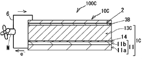
- the photosensitive layer has an upper surface of the conductive support through another layer, for example, a mode in which the photosensitive layer is provided in the form of a thin film on the surface of the porous layer (see FIG. 1). )
- An embodiment provided thick on the surface of the porous layer see FIG. 2), an embodiment provided thin on the surface of the blocking layer, and an embodiment provided thick on the surface of the blocking layer (see FIG. 3).
- the photosensitive layer may be provided in a linear or dispersed form, but is preferably provided in a film form.
- the photoelectric conversion element of the present invention is not particularly limited in structure other than the structure defined in the present invention, and known structures relating to the photoelectric conversion element and the solar cell can be adopted.
- Each layer constituting the photoelectric conversion element of the present invention is designed according to the purpose, and may be formed in a single layer or multiple layers, for example.
- the same reference numerals mean the same components (members).
- 1 and 2 show the size of the fine particles forming the porous layer with emphasis. These fine particles are preferably packed horizontally and vertically with respect to the conductive substrate to form a porous structure.
- photoelectric conversion element 10 means the photoelectric conversion elements 10A, 10B, and 10C unless otherwise specified.
- hole transport layer 3 means the hole transport layers 3A and 3B unless otherwise specified.
- a photoelectric conversion element 10A shown in FIG. 1 is a system applied to a battery for causing an operation circuit M (for example, an electric motor) to perform work by the external circuit 6 using the photoelectric conversion element 10A.
- This photoelectric conversion element 10A has a first electrode 1A, a second electrode 2, and a hole transport layer 3A containing a hole transport material described later between the first electrode 1A and the second electrode 2.
- 1 A of 1st electrodes have the electroconductive support body 11 which consists of the support body 11a and the transparent electrode 11b, Preferably the porous layer 12 and the photosensitive layer 13A.
- the blocking layer 14 is preferably provided on the transparent electrode 11 b, and the porous layer 12 is formed on the blocking layer 14.
- the photoelectric conversion element 10B shown in FIG. 2 schematically shows a preferred embodiment in which the photosensitive layer 13A of the photoelectric conversion element 10A shown in FIG. In the photoelectric conversion element 10B, the hole transport layer 3B is thinly provided.
- the photoelectric conversion element 10B differs from the photoelectric conversion element 10A shown in FIG. 1 in the film thicknesses of the photosensitive layer 13B and the hole transport layer 3B, but is configured in the same manner as the photoelectric conversion element 10A except for these points. ing.
- a photoelectric conversion element 10C shown in FIG. 3 schematically shows another preferred embodiment of the photoelectric conversion element of the present invention.
- the photoelectric conversion element 10C is different from the photoelectric conversion element 10B illustrated in FIG. 2 in that the porous layer 12 is not provided, but is configured in the same manner as the photoelectric conversion element 10B except for this point. That is, in the photoelectric conversion element 10 ⁇ / b> C, the photosensitive layer 13 ⁇ / b> C is formed on the surface of the blocking layer 14.
- the system 100 to which the photoelectric conversion element 10 is applied functions as a solar cell as follows. That is, in the photoelectric conversion element 10, light that has passed through the conductive support 11 or the second electrode 2 and entered the photosensitive layer 13 excites the light absorber. The excited light absorber has high-energy electrons, and these electrons reach the conductive support 11 from the photosensitive layer 13. At this time, the light absorber that has released electrons with high energy is an oxidant. Electrons reaching the conductive support 11 return to the photosensitive layer 13 via the second electrode 2 and then the hole transport layer 3 while working in the external circuit 6. The light absorber is reduced by the electrons returning to the photosensitive layer 13. By repeating excitation and electron transfer of the light absorber, the system 100 functions as a solar cell.
- the flow of electrons from the photosensitive layer 13 to the conductive support 11 differs depending on the presence and type of the porous layer 12 and the like.
- the porous layer 12 can be formed with an insulator other than the conventional semiconductor.
- the porous layer 12 is formed of a semiconductor, electron conduction in which electrons move inside or between the semiconductor particles of the porous layer 12 also occurs.
- the porous layer 12 is formed of an insulator, electron conduction in the porous layer 12 does not occur.
- the porous layer 12 is formed of an insulator
- a relatively high electromotive force (Voc) can be obtained by using aluminum oxide (Al 2 O 3 ) particles as the insulator particles.
- Al 2 O 3 aluminum oxide
- the blocking layer 14 as the other layer is formed of a conductor or a semiconductor, electron conduction in the blocking layer 14 occurs.
- the photoelectric conversion element and the solar cell of the present invention are not limited to the above-described preferred embodiments, and the configuration of each embodiment can be appropriately combined between the respective embodiments without departing from the spirit of the present invention.
- materials and members used for the photoelectric conversion element or solar cell can be prepared by a conventional method except for the light absorber and the hole transport layer 3.
- Patent Document 1 and Non-Patent Documents 1 to 3 can be referred to.
- dye-sensitized solar cells for example, Japanese Patent Application Laid-Open No. 2001-291534, US Pat. No. 4,927,721, US Pat. No. 4,684,537, US Pat. No. 5,084, 365, US Pat. No. 5,350,644, US Pat. No. 5,463,057, US Pat. No. 5,525,440, JP-A-7-249790, JP 2004-220974 A and JP 2008-135197 A can be referred to.
- the first electrode 1 has a conductive support 11 and a photosensitive layer 13 and functions as a working electrode in the photoelectric conversion element 10.
- the first electrode 1 preferably has one or both of the porous layer 12 and the blocking layer 14, and more preferably has at least the blocking layer 14.
- the conductive support 11 is not particularly limited as long as it has conductivity and can support the photosensitive layer 13 and the like.
- the conductive support 11 is composed of a conductive material, for example, a metal, or a glass or plastic support 11a and a transparent electrode 11b as a conductive film formed on the surface of the support 11a.
- the structure having is preferable.
- a conductive support 11 in which a transparent metal electrode 11b is formed by coating a conductive metal oxide on the surface of a glass or plastic support 11a is more preferable.
- the support 11a formed of plastic include a transparent polymer film described in paragraph No. 0153 of JP-A-2001-291534.
- ceramic Japanese Patent Laid-Open No. 2005-135902
- conductive resin Japanese Patent Laid-Open No. 2001-160425
- tin oxide As the metal oxide, tin oxide (TO) is preferable, and fluorine-doped tin oxide such as indium-tin oxide (tin-doped indium oxide; ITO) and fluorine-doped tin oxide (FTO) is particularly preferable.
- the coating amount of the metal oxide at this time is preferably 0.1 to 100 g per 1 m 2 of the surface area of the support 11a. When the conductive support 11 is used, light is preferably incident from the support 11a side.
- the conductive support 11 is preferably substantially transparent.
- “substantially transparent” means that the transmittance of light (wavelength 300 to 1200 nm) is 10% or more, preferably 50% or more, and particularly preferably 80% or more.
- the thicknesses of the support 11a and the conductive support 11 are not particularly limited, and are set to appropriate thicknesses.
- the thickness is preferably 0.01 ⁇ m to 10 mm, more preferably 0.1 ⁇ m to 5 mm, and particularly preferably 0.3 ⁇ m to 4 mm.
- the film thickness of the transparent electrode 11b is not particularly limited, and is preferably 0.01 to 30 ⁇ m, more preferably 0.03 to 25 ⁇ m, and more preferably 0.05 to 20 ⁇ m. It is particularly preferred that
- the conductive support 11 or the support 11a may have a light management function on the surface.
- the surface of the conductive support 11 or the support 11a may have an antireflection film in which high refractive films and low refractive index oxide films are alternately stacked as described in JP-A-2003-123859.
- the light guide function described in JP-A-2002-260746 may be provided.
- the blocking layer 14 is provided on the surface of the transparent electrode 11b, that is, between the conductive support 11 and the porous layer 12 or the hole transport layer 3 or the like. Yes.
- the blocking layer 14 functions to prevent this reverse current.
- the blocking layer 14 is also referred to as a short circuit prevention layer.
- the material for forming the blocking layer 14 is not particularly limited as long as it is a material capable of fulfilling the above function, but is a substance that transmits visible light and is an insulating substance for the conductive support 11 (transparent electrode 11b).
- the “insulating substance with respect to the conductive support 11 (transparent electrode 11b)” specifically refers to a material whose conduction band energy level forms the conductive support 11 (metal oxide forming the transparent electrode 11b).
- a compound (n-type semiconductor compound) that is higher than the energy level of the conduction band of the material and lower than the energy level of the conduction band of the material constituting the porous layer 12 and the ground state of the light absorber.
- Examples of the material for forming the blocking layer 14 include silicon oxide, magnesium oxide, aluminum oxide, calcium carbonate, polyvinyl alcohol, and polyurethane.
- the material generally used for the photoelectric conversion material may be used, and examples thereof include titanium oxide, tin oxide, niobium oxide, and tungsten oxide. Of these, titanium oxide, tin oxide, magnesium oxide, aluminum oxide and the like are preferable.
- the thickness of the blocking layer 14 is preferably 0.001 to 10 ⁇ m, more preferably 0.005 to 1 ⁇ m, and particularly preferably 0.01 to 0.1 ⁇ m.
- the porous layer 12 is preferably provided on the transparent electrode 11b.
- the porous layer 12 is formed on the blocking layer 14.
- the porous layer 12 is a layer that functions as a scaffold for carrying the photosensitive layer 13 on the surface.
- it is preferable to increase the surface area of at least a portion that receives light such as sunlight, and it is preferable to increase the entire surface area of the porous layer 12.
- the porous layer 12 is preferably a fine particle layer having pores, in which fine particles of the material forming the porous layer 12 are deposited or adhered.
- the porous layer 12 may be a fine particle layer in which two or more kinds of multi-fine particles are deposited.
- the amount of light absorbent supported (adsorption amount) can be increased.
- the surface area of the porous layer 12 it is preferable to increase the surface area of the individual fine particles constituting the porous layer 12.
- the surface area of the fine particles is preferably 10 times or more, more than 100 times the projected area. It is more preferable.
- the particle diameter of the fine particles forming the porous layer 12 is preferably 0.001 to 1 ⁇ m as the primary particle in the average particle diameter using the diameter when the projected area is converted into a circle.
- the average particle diameter of the fine particles is preferably 0.01 to 100 ⁇ m as the average particle diameter of the dispersion.
- the material for forming the porous layer 12 is not particularly limited with respect to conductivity, and may be an insulator (insulating material), a conductive material, or a semiconductor (semiconductive material). .
- Examples of the material for forming the porous layer 12 include metal chalcogenides (eg, oxides, sulfides, selenides, etc.), compounds having a perovskite crystal structure (excluding a light absorber described later), and oxidation of silicon.
- An object for example, silicon dioxide, zeolite), or carbon nanotube (including carbon nanowire and carbon nanorod) can be used.
- the metal chalcogenide is not particularly limited, but is preferably titanium, tin, zinc, tungsten, zirconium, hafnium, strontium, indium, cerium, yttrium, lanthanum, vanadium, niobium, aluminum or tantalum oxide, cadmium sulfide. , Cadmium selenide and the like.
- Examples of the crystal structure of the metal chalcogenide include an anatase type, brookite type and rutile type, and anatase type and brookite type are preferable.
- the compound having a perovskite crystal structure is not particularly limited, and examples thereof include transition metal oxides.
- transition metal oxides For example, strontium titanate, calcium titanate, barium titanate, lead titanate, barium zirconate, barium stannate, lead zirconate, strontium zirconate, strontium tantalate, potassium niobate, bismuth ferrate, strontium barium titanate , Barium lanthanum titanate, calcium titanate, sodium titanate, bismuth titanate.
- strontium titanate, calcium titanate and the like are preferable.
- the carbon nanotube has a shape obtained by rounding a carbon film (graphene sheet) into a cylindrical shape.
- Carbon nanotubes are single-walled carbon nanotubes (SWCNT) in which one graphene sheet is wound in a cylindrical shape, double-walled carbon nanotubes (DWCNT) in which two graphene sheets are wound in a concentric shape, and multiple graphene sheets are concentric
- SWCNT single-walled carbon nanotubes
- DWCNT double-walled carbon nanotubes
- MWCNT multi-walled carbon nanotubes
- any carbon nanotube is not particularly limited and can be used.
- the material for forming the porous layer 12 is preferably titanium, tin, zinc, zirconium, aluminum or silicon oxide, or carbon nanotube, more preferably titanium oxide or aluminum oxide.
- the porous layer 12 may be formed of at least one of the above-described metal chalcogenide, compound having a perovskite crystal structure, silicon oxide, and carbon nanotube, and may be formed of a plurality of types. .
- the material for forming the porous layer 12 is preferably used as fine particles as described later.
- the material forming the porous layer 12 includes a metal chalcogenide, a compound having a perovskite crystal structure, and a silicon oxide nanotube, nanowire or nanorod, a metal chalcogenide, a compound having a perovskite crystal structure, a silicon oxide. It can also be used with fine particles of carbon nanotubes.
- the film thickness of the porous layer 12 is not particularly limited, but is usually in the range of 0.1 to 100 ⁇ m. When used as a solar cell, 0.1 to 50 ⁇ m is preferable, and 0.3 to 30 ⁇ m is more preferable.
- the film thickness of the porous layer 12 is a lower layer surface on which the porous layer 12 is formed along a linear direction intersecting at an angle of 90 ° with the surface of the conductive support 11 in the cross section of the photoelectric conversion element 10. Defined by the average distance from the surface of the porous layer 12 to the surface of the porous layer 12.
- the “lower surface on which the porous layer 12 is formed” means the interface between the conductive support 11 and the porous layer 12.
- another layer such as the blocking layer 14 is formed between the conductive support 11 and the porous layer 12, it means the interface between the other layer and the porous layer 12.
- the “surface of the porous layer 12” is a porous layer located closest to the second electrode 2 from the conductive support 11 on a virtual straight line that intersects the surface of the conductive support 11 at an angle of 90 °. It refers to the point of the layer 12 (intersection of the virtual straight line and the contour line of the porous layer 12).
- the “average distance” is 10 in an observation region of a specific range in the cross section of the photoelectric conversion element 10 along a horizontal (parallel) direction (left-right direction in FIGS. 1 to 3) with respect to the surface of the conductive support 11.
- the longest distance from the surface of the lower layer to the surface of the porous layer 12 is obtained for each equally divided section, and the average value of the longest distances of these 10 sections is obtained.
- the film thickness of the porous layer 12 can be measured by observing the cross section of the photoelectric conversion element 10 with a scanning electron microscope (SEM). Unless otherwise stated, the thickness of other layers such as the blocking layer 14 can be measured in the same manner.
- the photosensitive layer 13 is a surface of the porous layer 12 (photoelectric conversion elements 10A and 10B) or the blocking layer 14 (photoelectric conversion element 10C) using a perovskite compound (to be described later) as a light absorber. (Including the inner surface when the surface is uneven).
- the light absorber only needs to contain at least one perovskite compound, and may contain two or more perovskite compounds.
- the photosensitive layer 13 may be a single layer or a laminate of two or more layers. When the photosensitive layer 13 has a laminated structure of two or more layers, layers composed of different light absorbers may be laminated, and an intermediate layer containing a hole transport material is laminated between the photosensitive layer and the photosensitive layer. May be.
- the form that the photosensitive layer 13 has on the conductive support 11 is as described above.
- the photosensitive layer 13 is preferably provided on the porous layer 12 or the blocking layer 14 so that excited electrons flow to the conductive support 11.
- the photosensitive layer 13 may be provided on the entire surface of the porous layer 12 or the blocking layer 14, or may be provided on a part of the surface.
- the film thickness of the photosensitive layer 13 is appropriately set according to the mode having the photosensitive layer 13 on the conductive support 11 and is not particularly limited.
- the film thickness of the photosensitive layer 13 (when the porous layer 12 is provided, the total film thickness with the porous layer 12) is preferably 0.1 to 100 ⁇ m, more preferably 0.1 to 50 ⁇ m, and 0 .3 to 30 ⁇ m is particularly preferable.
- the film thickness of the photosensitive layer 13 can be measured in the same manner as the film thickness of the porous layer 12.
- the thickness of the photosensitive layer 13 is the interface between the porous layer 12 and the hole transport layer 3 along the direction perpendicular to the surface of the porous layer 12. And the distance.
- the photoelectric conversion element 10B illustrated in FIG. 2 includes a photosensitive layer 13B having a thickness larger than that of the photosensitive layer 13A of the photoelectric conversion element 10A illustrated in FIG.
- the perovskite compound as the light absorber can be a hole transporting material, similar to the compound having the perovskite crystal structure as the material for forming the porous layer 12 described above.
- the photosensitive layer 13 includes, as a light absorber, “periodic table group 1 element or cationic organic group A”, “metal atom M other than periodic table group 1 element”, and “anionic atom X”. Containing a perovskite compound.
- the periodic table group 1 element or the cationic organic group A, the metal atom M, and the anionic atom X of the perovskite compound are each a cation (for convenience, sometimes referred to as cation A), a metal cation (for convenience).
- cation M a metal cation
- anion sometimes referred to as anion X for convenience.
- the cationic organic group means an organic group having a property of becoming a cation in the perovskite crystal structure
- the anionic atom means an atom having a property of becoming an anion in the perovskite crystal structure.
- the light absorber only needs to contain at least one perovskite compound. In this case, one kind of perovskite compound may be used alone, or two or more kinds of perovskite compounds may be used in combination.
- the perovskite compound is not particularly limited as long as it is a compound that can have a perovskite crystal structure containing the above constituent ions.
- the cation A is a cation of a group 1 element of the periodic table or an organic cation composed of a cationic organic group A.
- the cation A is preferably an organic cation.
- the cation of the Group 1 element of the periodic table is not particularly limited, and for example, the cation (Li + , Na + , K + of each element of lithium (Li), sodium (Na), potassium (K), or cesium (Cs). Cs + ), and a cesium cation (Cs + ) is particularly preferable.
- the organic cation is more preferably an organic cation of a cationic organic group represented by the following formula (1).
- R 1a represents a substituent.
- R 1a is not particularly limited as long as it is an organic group, but an alkyl group, a cycloalkyl group, an alkenyl group, an alkynyl group, an aryl group, a heteroaryl group, or a group that can be represented by the following formula (2) preferable.
- an alkyl group and a group that can be represented by the following formula (2) are more preferable.
- Xa represents NR ⁇ 1c> , an oxygen atom, or a sulfur atom.
- R 1b and R 1c each independently represent a hydrogen atom or a substituent.
- *** represents a bonding position with N in the formula (1).
- the organic cation of the cationic organic group A is preferably an organic ammonium cation composed of an ammonium cationic organic group A formed by bonding R 1a and NH 3 in the above formula (1).
- the organic ammonium cation can have a resonance structure
- the organic cation includes a cation having a resonance structure in addition to the organic ammonium cation.
- X a is NH (R 1c is a hydrogen atom)
- the organic cation is bonded to the group that can be represented by the above formula (2) and NH 3.
- an organic amidinium cation which is one of the resonance structures of the organic ammonium cation is also included.
- Examples of the organic amidinium cation comprising an amidinium cationic organic group include a cation represented by the following formula (A am ). Note that in this specification, a cation represented by the following formula (A am ) may be expressed as “R 1b C ( ⁇ NH) —NH 3 ” for convenience.
- the alkyl group is preferably an alkyl group having 1 to 18 carbon atoms, and more preferably an alkyl group having 1 to 6 carbon atoms.
- methyl, ethyl, propyl, isopropyl, butyl, tert-butyl, pentyl, hexyl and the like can be mentioned.
- the cycloalkyl group is preferably a cycloalkyl group having 3 to 8 carbon atoms, and examples thereof include cyclopropyl, cyclopentyl, and cyclohexyl.
- the alkenyl group is preferably an alkenyl group having 2 to 18 carbon atoms, and examples thereof include vinyl, allyl, butenyl and hexenyl.
- the alkynyl group is preferably an alkynyl group having 2 to 18 carbon atoms, and examples thereof include ethynyl, butynyl and hexynyl.
- the aryl group is preferably an aryl group having 6 to 14 carbon atoms, and examples thereof include phenyl.
- the heteroaryl group includes a group consisting only of an aromatic heterocycle and a group consisting of a condensed heterocycle obtained by condensing an aromatic heterocycle with another ring such as an aromatic ring, an aliphatic ring or a heterocycle.
- a ring-constituting hetero atom constituting the aromatic hetero ring a nitrogen atom, an oxygen atom and a sulfur atom are preferable.
- the number of ring members of the aromatic heterocycle is preferably a 5-membered ring or a 6-membered ring.
- Examples of the condensed heterocycle including a 5-membered aromatic heterocycle and a 5-membered aromatic heterocycle include a pyrrole ring, an imidazole ring, a pyrazole ring, an oxazole ring, a thiazole ring, a triazole ring, a furan ring, and a thiophene ring. , Benzimidazole ring, benzoxazole ring, benzothiazole ring, indoline ring, and indazole ring.
- Examples of the condensed heterocycle including a 6-membered aromatic heterocycle and a 6-membered aromatic heterocycle include, for example, pyridine ring, pyrimidine ring, pyrazine ring, triazine ring, quinoline ring, and quinazoline ring. Is mentioned.
- X a represents NR 1c , an oxygen atom or a sulfur atom, and NR 1c is preferable.
- R 1c is preferably a hydrogen atom, an alkyl group, a cycloalkyl group, an alkenyl group, an alkynyl group, an aryl group or a heteroaryl group, and more preferably a hydrogen atom.
- R 1b represents a hydrogen atom or a substituent, and preferably a hydrogen atom.
- R 1b can take include a hydrogen atom, an alkyl group, a cycloalkyl group, an alkenyl group, an alkynyl group, an aryl group, and a heteroaryl group.
- the alkyl group, cycloalkyl group, alkenyl group, alkynyl group, aryl group, heteroaryl group and group that can be represented by the above formula (2), which can be represented by R 1a , may have a substituent. Good.
- the substituent that R 1a may have is not particularly limited, and examples thereof include an alkyl group, a cycloalkyl group, an alkenyl group, an alkynyl group, an aryl group, a heterocyclic group, an alkoxy group, an alkylthio group, an amino group, Examples include alkylamino group, arylamino group, acyl group, alkoxycarbonyl group, aryloxycarbonyl group, acylamino group, sulfonamido group, carbamoyl group, sulfamoyl group, halogen atom, cyano group, hydroxy group or carboxy group. Each substituent that R 1a may have may be further substituted with a substituent.
- the metal cation M is not particularly limited as long as it is a cation of a metal atom M other than a group 1 element of the periodic table and a cation of a metal atom capable of taking a perovskite crystal structure.
- metal atoms include calcium (Ca), strontium (Sr), cadmium (Cd), copper (Cu), nickel (Ni), manganese (Mn), iron (Fe), cobalt (Co), Examples include palladium (Pd), germanium (Ge), tin (Sn), lead (Pb), ytterbium (Yb), europium (Eu), and indium (In).
- the metal atom M is particularly preferably Pb or Sn.
- M may be one type of metal atom or two or more types of metal atoms. In the case of two or more kinds of metal atoms, two kinds of Pb and Sn are preferable.
- the ratio of the metal atom at this time is not specifically limited.
- the anion X represents an anion of the anionic atom X.
- This anion is preferably an anion of a halogen atom.
- a halogen atom a fluorine atom, a chlorine atom, a bromine atom, an iodine atom, etc. are mentioned, for example.
- the anion X may be an anion of one kind of anionic atom or an anion of two or more kinds of anionic atoms.
- anions of two or more types of anionic atoms two types of anions of halogen atoms, particularly anions of bromine atoms and iodine atoms are preferred.
- the ratio of the anion of the anionic atom at this time is not particularly limited.
- the perovskite compound used in the present invention is preferably a perovskite compound having a perovskite crystal structure having the above-described constituent ions and represented by the following formula (I).
- A represents a group 1 element of the periodic table or a cationic organic group.
- M represents a metal atom other than Group 1 elements of the periodic table.
- X represents an anionic atom.
- a represents 1 or 2
- the Group 1 element of the periodic table or the cationic organic group A forms the cation A having a perovskite crystal structure. Accordingly, the Group 1 element of the periodic table and the cationic organic group A are not particularly limited as long as they are elements or groups that can form the perovskite crystal structure by becoming the cation A.
- the Periodic Table Group 1 element or the cationic organic group A has the same meaning as the Periodic Table Group 1 element or the cationic organic group described above for the cation A, and the preferred ones are also the same.
- the metal atom M is a metal atom that forms the metal cation M having a perovskite crystal structure. Therefore, the metal atom M is not particularly limited as long as it is an atom other than the Group 1 element of the periodic table and can form the perovskite crystal structure by becoming the metal cation M.
- the metal atom M is synonymous with the metal atom described in the metal cation M, and the preferred ones are also the same.
- the anionic atom X forms the anion X having a perovskite crystal structure. Therefore, the anionic atom X is not particularly limited as long as it is an atom that can form the perovskite crystal structure by becoming the anion X.
- the anionic atom X is synonymous with the anionic atom demonstrated with the said anion X, and its preferable thing is also the same.
- the perovskite compound represented by formula (I) is a perovskite compound represented by the following formula (I-1) when a is 1, and when a is 2, the perovskite compound represented by formula (I-2) It is a perovskite compound represented.
- A represents a group 1 element of the periodic table or a cationic organic group, and is synonymous with A in the formula (I), and preferred ones are also the same.
- M represents a metal atom other than the Group 1 element of the periodic table, and is synonymous with M in the above formula (I), and preferred ones are also the same.
- X represents an anionic atom, and is synonymous with X of the said formula (I), and its preferable thing is also the same.
- FIG. 4A is a diagram showing a basic unit cell of a perovskite crystal structure
- FIG. 4B is a diagram showing a structure in which the basic unit cell is three-dimensionally continuous in the perovskite crystal structure
- FIG. 4C is a diagram showing a layered structure in which inorganic layers and organic layers are alternately stacked in a perovskite crystal structure.
- the perovskite compound represented by the formula (I-1) as shown in FIG.
- a cation A is arranged at each apex, a metal cation M is arranged at the body center, and the metal cation M is the center.
- the basic unit cell has a continuous structure.
- the perovskite compound represented by the formula (I-2) has an MX 6 octahedron composed of a metal cation M and an anion X with respect to the perovskite compound represented by the formula (I-1). Same in respect, but different in basic unit cell and its arrangement. That is, the perovskite compound represented by the formula (I-2) is an inorganic layer formed by arranging MX 6 octahedrons in a two-dimensional (planar) form as shown in FIG. 4 (c). And an organic layer formed by alternately inserting a cation A between the inorganic layers.
- the basic unit cell shares the cation A and the anion X with other adjacent basic unit cells in the plane of the same layer.
- the basic unit cell does not share the cation A and the anion X in different layers.
- This layered structure has a two-dimensional layer structure in which the inorganic layer is divided by the organic group of the cation A. As shown in FIG. 4C, the organic group in the cation A functions as a spacer organic group between the inorganic layers.
- perovskite compounds having a layered structure see, for example, New. J. et al. Chem. , 2008, 32, 1736.
- a possible crystal structure is determined by the cation A (group 1 element of the periodic table or cationic organic group A).
- the cation A is a cation of a group 1 element of the periodic table or an organic cation of a cationic organic group A having a substituent R 1a having 1 carbon atom
- the perovskite compound is represented by the formula (I-1) It is easy to take a cubic crystal structure.
- Examples of such a cation A include CH 3 —NH 3 and each cation such as HC ( ⁇ NH) —NH 3 among organic cations having a group that can be represented by the formula (2). .
- the perovskite compound is represented by the formula (I-2) and easily takes a layered crystal structure.
- a cation A include an alkyl group having 2 or more carbon atoms, a cycloalkyl group, an alkenyl group, an alkynyl group, an aryl group, a heteroaryl group, and the following formula (2) described as the substituent R 1a.
- an organic cation of the cationic organic group A having a group capable of being substituted provided that R 1b and R 1c are substituents).
- the perovskite compound used in the present invention may be either a compound represented by formula (I-1) or a compound represented by formula (I-2), or a mixture thereof. Therefore, in the present invention, at least one perovskite compound only needs to be present as a light absorber, and it is not necessary to clearly distinguish which compound is strictly based on the composition formula, molecular formula, crystal structure, and the like. .
- the compound represented by the formula (I-1) and the compound represented by the formula (I-2) are described separately.
- the compounds exemplified as the compound represented by the formula (I-1) may be a compound represented by the formula (I-2) depending on the synthesis conditions and the like.
- the mixture is a mixture of the compound represented by -1) and the compound represented by formula (I-2).
- the compounds exemplified as the compound represented by the formula (I-2) may be a compound represented by the formula (I-1), and may be represented by the formula (I-1).
- the mixture is a mixture of the compound represented by formula (I-2).
- Specific examples of the compound represented by the formula (I-2) include, for example, (C 2 H 5 NH 3 ) 2 PbI 4 , (CH 2 ⁇ CHNH 3 ) 2 PbI 4 , (CH ⁇ CNH 3 ) 2 PbI 4 , (N-C 3 H 7 NH 3 ) 2 PbI 4 , (n-C 4 H 9 NH 3 ) 2 PbI 4 , (C 6 H 5 NH 3 ) 2 PbI 4 , (C 6 H 3 F 2 NH 3 ) 2 PbI 4 , (C 6 F 5 NH 3 ) 2 PbI 4 , (C 4 H 3 SNH 3 ) 2 PbI 4 .
- C 4 H 3 SNH 3 in (C 4 H 3 SNH 3) 2 PbI 4 is aminothiophene.
- the perovskite compound can be synthesized from MX 2 and AX.
- the said nonpatent literature 1 is mentioned.
- Akihiro Kojima, Kenjiro Teshima, Yasuo Shirai, and Tsutomu Miyasaka “Organometric Halide Perovskits as Visible Slight-Lights. Am. Chem. Soc. , 2009, 131 (17), 6050-6051.
- the amount of the light absorber used may be at least a part of the surface of the porous layer 12 or the blocking layer 14 on which light is incident, and is preferably an amount covering the entire surface.
- the hole transport layer 3 has a function of replenishing electrons to the oxidant of the light absorber, and is preferably a solid layer.
- the hole transport layer 3 is preferably provided between the photosensitive layer 13 of the first electrode 1 and the second electrode 2.
- the hole transport layer 3 has a HOMO energy level (energy level of the highest occupied orbit (energy level)) determined by density functional theory (DFT) calculation. At least one hole transport material falling within the range of ⁇ 4.50 to ⁇ 5.00 eV. In this case, one kind of the hole transport material may be used alone, or two or more kinds of the hole transport materials may be used in combination.
- the DFT calculation is performed by Gaussian 09 using B3LYP as the functional and 3-21G as the basis function.
- the HOMO energy level obtained by DFT calculation is preferably within the range of ⁇ 4.60 to ⁇ 5.00 eV, and more preferably within the range of ⁇ 4.60 to ⁇ 4.80 eV.
- the energy level of HOMO corresponds to the ionization energy.
- the ionization energy can be obtained by ultraviolet photoelectron spectroscopy (UPS) or the like.
- UPS ultraviolet photoelectron spectroscopy
- a single film of a hole transport material to be measured is formed on a glass substrate, and the single film is, for example, ESCA 5600 UPS (ultraviolet photoemission spectroscopy) manufactured by ULVAC-PHI Co., Ltd. Measure using the measuring device.
- the hole transport material used in the present invention has any structure of hole transport as long as the HOMO energy level obtained by DFT calculation falls within the range of ⁇ 4.50 to ⁇ 5.00 eV. It may be a material. For example, it may be a polymer or oligomer, or a monomer, that is, a compound that is not a polymer compound. In the present invention, a hole transport material that is not a polymer compound is preferred.
- the molecular weight of the hole transport material that is not a polymer compound is, for example, preferably 400 to 10,000, more preferably 400 to 5,000, and still more preferably 400 to 3,000.
- the hole transport material is preferably an aryl or heteroarylamine compound in terms of the chemical structure of the compound, and is preferably a compound in which all the bonds of the nitrogen atom are bonded to the aryl group or heteroaryl group.
- compounds having 2 to 10 nitrogen atoms are preferred, compounds having 2 to 6 are more preferred, and compounds having 2 to 4 are more preferred.
- examples of the aryl group include a phenyl group and a naphthyl group.
- a heteroaryl group includes a group consisting of an aromatic heterocycle. This aromatic heterocycle is preferably a 5-membered ring or a 6-membered ring. As the ring-constituting hetero atom of the aromatic hetero ring, a sulfur atom, a nitrogen atom and an oxygen atom are preferable.
- the heteroaryl group also includes a group consisting of an aromatic hydrocarbon ring such as a benzene ring or a condensed heterocycle in which a heterocycle is condensed to the aromatic heterocycle.
- heteroaryl group examples include thiophene ring, furan ring, pyrrole ring, pyrazole ring, imidazole ring, triazole ring, oxazole ring, thiazole ring, pyridine ring, pyrazine ring, pyrimidine ring, pyridazine ring and the like.
- the aryl group or heteroaryl group may have a substituent TD1 .
- substituent T D1 include an alkyl group, an alkenyl group, an alkynyl group, a cycloalkyl group, an aryl group, a heterocyclic group, an alkoxy group, an aryloxy group, an alkylthio group, an arylthio group, a hydroxy group, and an amino group.
- alkyl groups, alkoxy groups, alkylthio groups, alkylamino groups (preferably dialkylamino groups), arylamino groups (preferably diarylamino groups, N-alkyl-N-arylamino groups), alkyl-substituted silyl groups (Also referred to as an alkylsilyl group), an alkoxycarbonyl group, and an acyl group are preferable.
- An alkyl group, an alkoxy group, an alkylthio group, a dialkylamino group, a diarylamino group, an N-alkyl-N-arylamino group, and an alkyl-substituted silyl group preferable.
- the substituent that the aryl group or heteroaryl group may have is preferably a group having at least an alkyl moiety, and the alkyl moiety preferably has 2 or more carbon atoms.
- the number of carbon atoms in the alkyl moiety is more preferably 2 to 30, further preferably 2 to 20, and particularly preferably 2 to 12.
- a preferable compound as the hole transport material is a compound represented by the following formula (D).
- L D1 represents an “arylene group”, “heteroarylene group”, or “a linking group in which at least two of an arylene group and a heteroarylene group are combined”.
- Ar D1 to Ar D4 each independently represents an aryl group or a heteroaryl group.
- Ar D1 to Ar D4 may have a substituent.
- Ar D1 and Ar D2 , Ar D3 and Ar D4 may be bonded to each other to form a ring.
- Examples of the “arylene group” in L D1 include a phenylene group and a naphthylene group, and a phenylene group is preferable.
- the “heteroarylene group” in L D1 is preferably a divalent group of an aromatic heterocycle exemplified for the heteroaryl group of the heteroarylamine compound, and the preferred range is also the same.
- the “linking group in which at least two of the arylene group and heteroarylene group are combined” in L D1 may be a linking group in which the same kind of groups are combined, or a linking group in which different groups are combined.
- L D1 examples include a group in which a plurality of arylene groups are connected, a group in which a plurality of heteroarylene groups are connected, and a group in which arylene groups and heteroarylene groups are connected alternately, randomly, or in blocks.
- arylene groups and heteroarylene groups may have a substituent.
- substituents, the aryl and heteroaryl groups may also have substituent T D1 and the like.
- the linking group is a group in which a plurality of arylene groups or heteroarylene groups are linked
- adjacent rings may be linked to form a ring.
- a ring is preferably a 5-membered ring or a 6-membered ring, but may also be a spiro ring.
- the formed ring may be a carbocycle consisting of only carbon atoms or a heterocycle containing a silyl atom.
- an aromatic hydrocarbon ring such as a benzene ring or a hetero ring may be condensed to the formed ring.
- L D1 is preferably a group represented by any one of the following formulas (L-1) to (L-4).
- R La to R Lc each independently represent a substituent.
- n La represents an integer of 0 to 4
- n Lb and n Lc each independently represents an integer of 0 to 3.
- la represents an integer of 1 to 4.
- Q La represents a group that forms a 5-membered hydrocarbon ring or spiro ring, a group that forms a 6-membered hydrocarbon ring or spiro ring, or —Si (Rx) (Ry) —.
- Rx and Ry each independently represents an alkyl group.
- Y and Z each independently represents O, S or —CH ⁇ N—, Y is preferably —CH ⁇ N—, and Z is preferably S.
- R Lg1 and R Lg2 each independently represent a substituent.
- R Lf1 , R Lf2 , R Lh1 and R Lh2 each independently represent a hydrogen atom or a substituent.
- n Lg1 and n Lg2 each independently represents an integer of 0 to 4.
- lb represents an integer of 1 to 4. * Represents a bonding position with N in the formula (D).
- R La to R Lc , R Lg1, and R Lg2 examples include the substituent T D1 that the aryl group and heteroaryl group may have, and the preferred range is also the same.
- R Lf1 , R Lf2 , R Lh1 and R Lh2 are each preferably a hydrogen atom.
- examples of the substituent include the substituent T D1 that the aryl group and heteroaryl group may have, and the preferred range is also the same. is there.
- R Lf1 and R Lf2 (hereinafter referred to as R Lf ), and R Lh1 and R Lh2 (hereinafter referred to as R Lh ), respectively, are not bonded to each other and bonded to each other to form a ring. Is included.
- the ring formed by R Lf and R Lh is preferably a 5-membered ring or a 6-membered ring, and may be an aromatic ring or a heterocyclic ring.
- R Lf or R Lh is an alkenyl group
- R Lf or R Lh are bonded together to form a benzene together with a ring containing Y of formula (L-3) or a ring containing Z of formula (L-4)
- Rings can be formed.
- R Lf or R Lh is an alkoxy group
- R Lf or R Lh is bonded to each other to form 1 together with a ring containing Y of formula (L-3) or a ring containing Z of formula (L-4).
- 4-dioxane ring can be formed.
- n La , n Lb and n Lc , and n Lg1 and n Lg2 is preferably 0 or 1, more preferably 0.
- la is preferably 2 or 3.
- lb is preferably 2 or 3, more preferably 2.
- Rx and Ry are preferably an alkyl group having 1 to 18 carbon atoms, more preferably an alkyl group having 2 to 10 carbon atoms, and examples thereof include methyl, ethyl, hexyl, and octyl.
- Formula (L-2) including Q La is preferably a group represented by any one of the following formulas (L-2a) to (L-2f), and includes formula (L-2a) and formula (L -C) to a group represented by any one of formulas (L-2d) to (L-2d), more preferably a group represented by formula (L-2a) or (L-2c).
- R Lb, R Lc, n Lb and n Lc has the same meaning as R Lb, R Lc, n Lb and n Lc in Formula (L-2), and the preferred range is also the same.
- R Qa , R Qb , R Qc and R Qd are all synonymous with Rx and Ry in formula (L-2), and preferred ranges are also the same.
- R Qa and R Qb are more preferably methyl, ethyl and isopropyl, respectively, and R Qc and R Qd are more preferably ethyl and n-hexyl, respectively.
- the aryl group and heteroaryl group in Ar D1 to Ar D4 are synonymous with the aryl group and heteroaryl group of the heteroarylamine compound, and the preferred range is also the same.
- at least one of the aryl group or heteroaryl group in Ar D1 to Ar D4 preferably has the following substituent T D2 .
- At least one of the aryl or heteroaryl group as the substituent T D2 having preferably the following groups 1) or, include groups of the following 2).
- Examples of the group T D2-1 of 1) include an alkyl group, alkoxy group, alkylthio group, alkylamino group, dialkylamino group, alkoxycarbonyl group, alkylsilyl group, or acyl group having 2 or more carbon atoms.
- Examples of the group T D2-2 in 2) include an aryl group or a heteroaryl group substituted by the group T D2-1 in the above 1).
- Examples of the group T D2-1 in 1) include the above-described groups having 3 or more carbon atoms and the above-described groups having 4 or more carbon atoms.
- more preferable substituents include an alkyl group having 2 or more carbon atoms, an alkoxy group having 2 or more carbon atoms, an aryl group substituted by an alkyl group having 2 or more carbon atoms, or an alkoxy group having 2 or more carbon atoms.
- Examples include a substituted aryl group, a heteroaryl group substituted with an alkyl group having 2 or more carbon atoms, or a heteroaryl group substituted with an alkoxy group having 2 or more carbon atoms.
- Ar D1 is preferably a group represented by any one of the following formulas (R-1) to (R-3), and is represented by the formula (R-2) or the formula (R-3). More preferred are groups.
- X R represents CH or N.
- R Ra1 , R Ra2 , R Rb , R Rc and R Rf each independently represent a substituent.
- n Ra1 , n Rc and n Rf represent an integer of 0 to 4
- n Ra2 represents an integer of 0 to 5
- n Rb represents an integer of 0 to 3.
- R Rd and R Re each independently represent an alkyl group, and R Rd and R Re may be bonded to each other to form a ring. ** represents a bonding position with N in any one of formulas (D) and (D-1) to (D-4).
- R Ra1 and n Ra1 have the same meanings as R La1 and n La1 in formula (D-1) described later, and R Rb to R Re and n Rb denote R Lb to R Le and n in formula (D-2) to be described later. It is synonymous with Lb.
- R Ra2 and R Rc include substituents that the aryl group and heteroaryl group may have. In the present invention, it is more preferable that R Ra1 , R Ra2 , R Rb , R Rc and R Rf are each independently a substituent TD2 .
- Ar D2 to Ar D4 may each be a group represented by any one of the formulas (R-1) to (R-3).
- the compound represented by the above formula (D) that is, the hole transport material
- a compound represented by any one of the following formulas (D-1) to (D-4) is more preferable, and the battery performance is stabilized.
- the formula (D-2) is particularly preferable.
- Ar D1 ⁇ Ar D4 have the same meanings as Ar D1 ⁇ Ar D4 in the formula (D).
- R La1 , R La2 , R Lb and R Lc each independently represent a substituent.
- n La1 and n La2 each independently represent an integer of 0 to 4, and n Lb and n Lc each independently represent an integer of 0 to 3.
- R Ld and R Le each independently represents an alkyl group, and R Ld and R Le may be bonded to each other to form a ring.
- Y and Z each independently represents O, S or —CH ⁇ N—, Y is preferably —CH ⁇ N—, and Z is preferably S.
- R Lg1 and R Lg2 each independently represent a substituent.
- R Lf1 , R Lf2 , R Lh1 and R Lh2 each independently represent a hydrogen atom or a substituent.
- n Lg1 and n Lg2 each independently represents an integer of 0 to 4.
- lb represents an integer of 1 to 4.
- R La1 and n L1a have the same meanings as R La and n La in formula (L-1), and preferred ranges are also the same.
- R La2 and n L2a are synonymous with the corresponding R La1 and n L1a , and the preferred ranges are also the same.
- R Lb, R Lc, n Lb and n Lc are as defined R Lb, R Lc, n Lb and n Lc in Formula (L-2).
- R Ld and R Le have the same meanings as Rx and Ry in formula (L-2), and preferred ranges are also the same.
- Y has the same meaning as Y in formula (L-3), and the preferred range is also the same.
- Z has the same meaning as Z in formula (L-4), and the preferred range is also the same.
- R Lf1 and R Lf2 has the same meaning as R Lf1 and R Lf2 in (L-3), and the preferred range is also the same.
- R Lg1, R Lg2, R Lh1 and R Lh2 has the same meaning as R Lg1, R Lg2, R Lh1 and R Lh2 in formula (L-4), and the preferred range is also the same.
- n Lg1 and n Lg2 has the same meaning as n Lg1 and n Lg2 in formula (L-4), and the preferred range is also the same.
- the compound represented by the formula (D) has two condensed aromatic rings described in US Pat. No. 5,061,569 in the molecule, for example, 4,4 ′ -Bis [N- (1-naphthyl) -N-phenylamino] biphenyl (abbreviated as NPD), three triphenylamine units described in JP-A-4-308688 were linked in a starburst type 4,4 ′, 4 ′′ -tris [N- (3-methylphenyl) -N-phenylamino] triphenylamine (abbreviated as MTDATA) and the like.
- NPD N-naphthyl
- MTDATA triphenylamine
- the compound represented by the formula (D) can be synthesized according to the method described in Comprehensive Organic Synthesis-Selectivity, Strategie and efficiency in Modern Organic Chemistry.
- examples of the hole transport material that can be used in combination with the hole transport material having an energy level of HOMO in the range of ⁇ 4.50 to ⁇ 5.00 eV include inorganic materials such as CuI and CuNCS, And organic hole transport materials described in paragraph Nos. 0209 to 0212 of JP-A No. 2001-291534.
- organic hole transport material examples include polythiophene [for example, poly (3-hexylthiophene-2,5-diyl), polyethylenedioxythiophene (PEDOT)], and the energy level of HOMO is ⁇ 4.50 to ⁇
- Conductive polymers such as polyaniline, polypyrrole and polysilane which are outside the range of 5.00 eV, spiro compounds having two rings sharing a central atom such as C, Si and the like with a tetrahedral structure [for example, 2, 2 ′, 7 , 7'-tetrakis- (N, N-di-p-methoxyphenylamine) -9,9-spirobifluorene (Spiro-OMeTAD)], triarylamine and other aromatic amine compounds (for example, poly (triphenyl) Amine), 4- (diethylamino) benzaldehyde diphenylhydrazone), triphenylene compound, nitrogen-containing heterocycle Compound
- the hole transport material preferably contains only a hole transport material (compound) having a HOMO energy level in the range of ⁇ 4.50 to ⁇ 5.00 eV.
- a hole transport material having a HOMO energy level outside the range of ⁇ 4.50 to ⁇ 5.00 eV is used in combination as the hole transport material, the hole transport material used in combination is all the hole transport materials used. Is 100 parts by mass or less, preferably 95 parts by mass or less, and more preferably 90 parts by mass or less.
- the hole transport material as a preferred embodiment of the present invention is a solid hole transport material that can be applied by solution, has excellent solubility, and is solid.
- the thickness of the hole transport layer 3 is not particularly limited, but is preferably 50 ⁇ m or less, more preferably 1 nm to 10 ⁇ m, further preferably 5 nm to 5 ⁇ m, and particularly preferably 10 nm to 1 ⁇ m.
- the film thickness of the hole transport layer 3 corresponds to the distance from the second electrode 2. This film thickness can be measured by observing the cross section of the photoelectric conversion element 10 using a scanning electron microscope (SEM) or the like.
- the total film thickness of the photosensitive layer 13 and the hole transport layer 3 (when having the porous layer 12, the total film thickness of the porous layer 12, the photosensitive layer 13, and the hole transport layer 3) is particularly It is not limited.
- the total film thickness is preferably 0.1 to 200 ⁇ m, more preferably 0.5 to 50 ⁇ m, and further preferably 0.5 to 5 ⁇ m.
- the second electrode 2 functions as a positive electrode in the solar cell.
- the 2nd electrode 2 will not be specifically limited if it has electroconductivity, Usually, it can be set as the same structure as the electroconductive support body 11. FIG. If the strength is sufficiently maintained, the support 11a is not necessarily required.
- the structure of the second electrode 2 is preferably a structure having a high current collecting effect. In order for light to reach the photosensitive layer 13, at least one of the conductive support 11 and the second electrode 2 must be substantially transparent. In the solar cell of this invention, it is preferable that the electroconductive support body 11 is transparent and sunlight is entered from the support body 11a side. In this case, it is more preferable that the second electrode 2 has a property of reflecting light.
- Examples of the material for forming the second electrode 2 include platinum (Pt), gold (Au), nickel (Ni), copper (Cu), silver (Ag), indium (In), ruthenium (Ru), palladium ( Examples thereof include metals such as Pd), rhodium (Rh), iridium (Ir), and osnium (Os), the above-described conductive metal oxides, and carbon materials.
- the carbon material may be a conductive material formed by bonding carbon atoms to each other, and examples thereof include fullerene, carbon nanotube, graphite, and graphene.
- the second electrode 2 is preferably glass or plastic having a metal or conductive metal oxide thin film (including a thin film formed by vapor deposition), glass having a thin film of Au or Pt, or glass vapor-deposited with Pt. Is particularly preferred.
- the film thickness of the second electrode 2 is not particularly limited, but is preferably 0.01 to 100 ⁇ m, more preferably 0.01 to 10 ⁇ m, and particularly preferably 0.01 to 1 ⁇ m.
- a spacer or a separator can be used instead of the blocking layer 14 or together with the blocking layer 14.
- a hole blocking layer may be provided between the second electrode 2 and the hole transport layer 3.
- the solar cell of the present invention is configured to cause the photoelectric conversion element 10 to work with respect to the external circuit 6 as shown in FIGS. 1 to 3, for example.
- the external circuit connected to the first electrode 1 (conductive support 11) and the second electrode 2 can be used without particular limitation.
- the solar cell to which the photoelectric conversion element of the present invention is applied is not particularly limited, and examples thereof include solar cells described in Patent Document 1 and Non-Patent Documents 1 to 3.
- the photoelectric conversion element and the solar cell according to the embodiment of the present invention can be manufactured according to a known manufacturing method, for example, a method described in Non-Patent Documents 1 to 3 and the like. Below, the manufacturing method of the photoelectric conversion element and solar cell concerning embodiment of this invention is demonstrated easily.
- the blocking layer 14 can be formed by, for example, a method of applying a dispersion containing the insulating material or a precursor compound thereof on the surface of the conductive support 11 and baking it, or a spray pyrolysis method.
- the material forming the porous layer 12 is preferably used as fine particles, and more preferably used as a dispersion containing fine particles.
- a method for forming the porous layer 12 is not particularly limited, and examples thereof include a wet method, a dry method, and other methods (for example, a method described in Chemical Review, Vol. 110, page 6595 (2010)). Can be mentioned.
- the dispersion (paste) is preferably applied to the surface of the conductive support 11 or the surface of the blocking layer 14 and then baked at a temperature of 100 to 800 ° C. for 10 minutes to 10 hours. Thereby, microparticles
- the firing temperature other than the last firing is preferably performed at a temperature lower than the last firing temperature (the last firing temperature).
- the firing temperature other than the last can be set within a range of 50 to 300 ° C.
- the final firing temperature can be set to be higher than the firing temperature other than the last within the range of 100 to 600 ° C.
- the firing temperature is preferably 60 to 500 ° C.
- the amount of the porous material applied when forming the porous layer 12 is appropriately set according to the thickness of the porous layer 12 to be formed, the number of times of application, and the like, and is not particularly limited.
- the coating amount of the porous material per 1 m 2 of the surface area of the conductive support 11 is preferably 0.5 to 500 g, more preferably 5 to 100 g.
- the photosensitive layer 13 is provided.
- a light absorbent solution for forming the photosensitive layer 13 is prepared.
- the light absorber solution contains MX 2 and AX, which are raw materials for the perovskite compound.
- A, M and X have the same meanings as A, M and X in the above formula (I).
- the molar ratio of MX 2 to AX is adjusted according to a or the like of the perovskite compound (P).
- the prepared light absorber solution is applied to the surface of the porous layer 12 or the surface of the blocking layer 14 and dried. Thereby, a perovskite compound is formed on the surface of the porous layer 12 or the surface of the blocking layer 14. Thereby, a perovskite compound is formed on the surface of the porous layer 12 or the surface of the blocking layer 14.
- a hole transport material solution containing a hole transport material is applied onto the photosensitive layer 13 thus provided, and dried to form the hole transport layer 3.
- the hole transport material solution has a coating solution concentration of 0.1 to 1.0 M in that it has excellent coating properties, and if it has the porous layer 12, it easily penetrates into the pores of the porous layer 12. (Mol / L) is preferred.
- the second electrode 2 is formed, and a photoelectric conversion element and a solar cell are manufactured.
- the film thickness of each layer can be adjusted by appropriately changing the concentration of each dispersion or solution and the number of coatings. For example, when the thick photosensitive layer 13B shown in FIG. 2 or FIG. 3 is provided, the dispersion may be applied and dried a plurality of times.
- Each of the above-mentioned dispersions and solutions may contain additives such as a dispersion aid and a surfactant as necessary.
- Examples of the solvent or dispersion medium used in the photoelectric conversion element and solar cell manufacturing method include, but are not limited to, the solvents described in JP-A No. 2001-291534.
- an organic solvent is preferable, and an alcohol solvent, an amide solvent, a nitrile solvent, a hydrocarbon solvent, a lactone solvent, and a mixed solvent of two or more of these are more preferable.
- the mixed solvent a mixed solvent of an alcohol solvent and a solvent selected from an amide solvent, a nitrile solvent, or a hydrocarbon solvent is preferable.
- methanol, ethanol, ⁇ -butyrolactone, chlorobenzene, acetonitrile, dimethylformamide (DMF) or dimethylacetamide, or a mixed solvent thereof is preferable.
- the application method of the solution or dispersant forming each layer is not particularly limited, and spin coating, extrusion die coating, blade coating, bar coating, screen printing, stencil printing, roll coating, curtain coating, spray coating, dip coating, inkjet
- a known coating method such as a printing method or a dipping method can be used. Of these, spin coating, screen printing, dipping, and the like are preferable.
- a solar cell is manufactured by connecting an external circuit to the first electrode 1 and the second electrode 2 of the photoelectric conversion element manufactured as described above.
- Example 1 The photoelectric conversion element 10A and the solar cell shown in FIG. 1 were manufactured by the following procedure. In addition, when the film thickness of the photosensitive layer 13 is large, it corresponds to the photoelectric conversion element 10B and the solar cell shown in FIG.
- a fluorine-doped SnO 2 conductive film (transparent electrode 11b) was formed on a glass substrate (support 11a, thickness 2.2 mm) to produce a conductive support 11.
- a blocking layer 14 (film thickness: 100 nm) was formed on the SnO 2 conductive film at 450 ° C. by spray pyrolysis using the prepared 0.02M blocking layer solution.
- the prepared titanium oxide paste was applied onto the blocking layer 14 by screen printing and baked.
- the titanium oxide paste was applied and fired twice. As the firing temperature, the first firing was performed at 130 ° C., and the second firing was performed at 500 ° C. for 1 hour.
- the obtained titanium oxide fired body was immersed in a 40 mM TiCl 4 aqueous solution and then heated at 60 ° C. for 1 hour and then at 500 ° C. for 30 minutes to form a porous layer 12 (thickness 500 nm) made of TiO 2. Was deposited.
- the prepared light absorbent solution A was applied onto the porous layer 12 by a spin coating method (2000 rpm for 60 seconds, followed by 3000 rpm for 60 seconds), and the applied light absorbent solution A was applied at 100 ° C. to 40 ° C. with a hot plate. It was dried for a minute to form photosensitive layer A (film thickness 600 nm) as photosensitive layer 13A having a perovskite compound.
- the obtained perovskite compound was CH 3 NH 3 PbI 3 .
- Formamidine acetate and an aqueous solution of 57% by mass hydrogen iodide containing 2 equivalents of hydrogen iodide with respect to formamidine acetate were stirred in a flask at 0 ° C. for 1 hour and then raised to 50 ° C. Warmed and stirred for an additional hour and mixed.
- the obtained solution was concentrated to obtain a crude formamidine hydrogen iodide.
- the obtained crude product was recrystallized with diethyl ether, and the precipitated crystals were collected by filtration and dried under reduced pressure at 50 ° C. for 10 hours to obtain purified formamidine hydrogen iodide salt.
- the prepared light absorber solution B was applied onto the porous layer 12 by a spin coating method (2000 rpm for 60 seconds, followed by 3000 rpm for 60 seconds).
- the applied light absorbent solution B was dried at 160 ° C. for 40 minutes by a hot plate to form a photosensitive layer B as a photosensitive layer 13A having a perovskite compound.
- the prepared light absorbent solution C was applied onto the porous layer 12 by a spin coating method (2000 rpm for 60 seconds, followed by 3000 rpm for 60 seconds).
- the applied light absorbent solution C was dried on a hot plate at 140 ° C. for 40 minutes to form a photosensitive layer C as a photosensitive layer 13A having a perovskite compound.
- the obtained perovskite compound was (CH 3 CH 2 —NH 3 ) 2 PbI 4 .
- ⁇ Preparation of hole transport material solution The hole transport material (180 mg) described in Table 1 below was dissolved in chlorobenzene (1 mL). To this chlorobenzene solution, an acetonitrile solution (37.5 ⁇ L) in which lithium-bis (trifluoromethanesulfonyl) imide (170 mg) was dissolved in acetonitrile (1 mL) and t-butylpyridine (TBP, 17.5 ⁇ L) were added. A hole transport material solution was prepared by mixing.
- the prepared hole transporting material solution is applied onto the photosensitive layer 13 of the first electrode 1 by spin coating, and the applied hole transporting material solution is dried to form a hole transporting layer 3 (thickness 0. 5 ⁇ m) was formed.
- each of the above film thicknesses was observed by SEM according to the above method, and an average of 10 categories within the observation range was obtained, and this value was defined as the film thickness.
- the initial performance was evaluated based on the initial conversion efficiency. Specifically, five solar cells of each sample number were manufactured under the same conditions, the photoelectric conversion efficiencies of the obtained five solar cells were calculated as described above, and the average value thereof was obtained. The obtained average value was used as the initial conversion efficiency of the solar cell of each sample number.
- the initial performance was evaluated according to the following evaluation criteria based on the initial conversion efficiency thus obtained. In the present invention, the initial performance is required to be evaluated as A, B + and B, and is preferably A for practical use.
- Evaluation of variation in initial performance was evaluated based on variations in initial conversion efficiency. Specifically, the standard deviation of the initial conversion efficiencies of five solar cells was determined for the solar cells of each sample number. Based on the standard deviation value of the initial conversion efficiency thus obtained, the variation in the initial performance was evaluated according to the following evaluation criteria.
- the evaluation of the variation in the initial performance is required to be A, B + and B, and is practically preferably A.
- A The standard deviation value of the initial conversion efficiency is less than 0.1 times the standard deviation value of the initial conversion efficiency of the following comparative compound R-2.
- B + The standard deviation value of the initial conversion efficiency is the following comparative compound R -0.1 to less than 0.2 times the standard deviation value of the initial conversion efficiency of B-2: the standard deviation value of the initial conversion efficiency is the standard deviation value of the initial conversion efficiency of the following comparative compound R-2 C: The standard deviation value of the initial conversion efficiency is 0.3 times or more the standard deviation value of the initial conversion efficiency of the following comparative compound R-2
- the hole transport material used for 201 and 202 is a compound having the following structure.
- the solar cell of the present invention may be a compound represented by the formula (I-1) or a compound represented by the formula (I-2) as a light absorber. It can be seen that when used together with the hole transport material (sample Nos. 101, 116 and 117), the photoelectric conversion efficiency is improved and the battery performance can be stably exhibited.
Landscapes
- Chemical & Material Sciences (AREA)
- Engineering & Computer Science (AREA)
- Materials Engineering (AREA)
- Physics & Mathematics (AREA)
- Spectroscopy & Molecular Physics (AREA)
- Photovoltaic Devices (AREA)
- Electroluminescent Light Sources (AREA)
Abstract
光電変換効率が向上し、しかも、繰り返し製造しても光電変換効率等の電池性能を安定して発揮する光電変換素子および太陽電池を提供する。光吸収剤を含む感光層を導電性支持体上に有する第一電極と、第一電極に対向する第二電極と、第一電極と第二電極の間に設けられた正孔輸送層とを有する光電変換素子であって、光吸収剤が、周期表第一族元素もしくはカチオン性有機基のカチオン、周期表第一族元素以外の金属原子Mのカチオンおよびアニオン性原子Xのアニオンを有するペロブスカイト型結晶構造を持つ化合物を含み、正孔輸送層が、密度汎関数理論計算による最高被占軌道のエネルギー準位が-4.50~-5.00eVの範囲内である正孔輸送材料を含有する光電変換素子、ならびに、この光電変換素子を有する太陽電池。
Description
本発明は、光電変換素子および太陽電池、特に、有機無機ハイブリッド固体光電変換素子およびそれを用いた太陽電池に関する。
光電変換素子は、各種の光センサー、複写機、太陽電池等に用いられている。この光電変換素子には、金属を用いた方式、半導体を用いた方式、有機顔料や色素を用いた方式、または、これらを組み合わせた方式等の様々な方式が実用化されている。特に、非枯渇性の太陽エネルギーを利用した太陽電池は、燃料が不要であり、無尽蔵のクリーンエネルギーを利用するものとして、その本格的な普及が大いに期待されている。
各国の政策的配慮等によって、太陽電池の中でも、シリコン系太陽電池、銅(Cu)、インジウム(In)、ガリウム(Ga)およびセレン(Se)を含む化合物を用いたCIGS系太陽電池、ならびに、カドミウム(Cd)およびテルル(Te)を含む化合物を用いたCdTe太陽電池等が普及してきている。しかし、火力発電や原子力発電に置き換わるレベルに普及するためには、更なる製造コストの低下が望まれている。
色素増感太陽電池や有機薄膜太陽電池は、その製造に真空プロセスを使用せず、塗布プロセスによって製造コストを大幅に低下できる可能性があることから、次世代太陽電池として期待され、精力的に検討されている。しかしながら、色素増感太陽電池や有機薄膜太陽電池は、光電変換効率が十分とはいえない。
一方、最近になって、感光層の光吸収剤としてペロブスカイト型結晶構造を有する鉛錯体と電解質とを組み合わせた太陽電池が提案された(特許文献1および非特許文献1参照)。その後、この鉛錯体を用いた太陽電池が、塗布プロセスで製造でき、かつ色素増感太陽電池や有機薄膜太陽電池と同等以上の光電変換効率を示すことが報告され(例えば、非特許文献2または3参照)、注目を集めている。
J.Am.Chem.Soc.,2009,131(17),6050-6051
Science,338,643(2012)
Nature Photonics Published Online,5,May,2013
本発明者らの検討によれば、ペロブスカイト結晶構造を有する化合物を用いた太陽電池は、無機素材のシリコンを使用する太陽電池と比較すると、光電変換効率のさらなる向上が必要であることがわかった。
これに加えて、ペロブスカイト結晶構造を有する化合物を用いた太陽電池は、得られた光電変換素子や太陽電池の性能が安定しない、すなわち、同じように製造した光電変換素子や太陽電池であっても同じ性能が得られない問題があることがわかった。
したがって、本発明は、光電変換効率が向上し、しかも、繰り返し製造しても光電変換効率等の電池性能を安定して発揮する光電変換素子および太陽電池を提供することを課題とする。
これに加えて、ペロブスカイト結晶構造を有する化合物を用いた太陽電池は、得られた光電変換素子や太陽電池の性能が安定しない、すなわち、同じように製造した光電変換素子や太陽電池であっても同じ性能が得られない問題があることがわかった。
したがって、本発明は、光電変換効率が向上し、しかも、繰り返し製造しても光電変換効率等の電池性能を安定して発揮する光電変換素子および太陽電池を提供することを課題とする。
本発明者らは、ペロブスカイト結晶構造を有する化合物を用いた太陽電池において、正孔輸送層に用いる材料の分子構造と物性に着目し、検討を行った結果、上記の課題解決への手掛りを得るに至り、本発明に至った。
すなわち、上記の課題は以下の手段により解決された。
<1>光吸収剤を含む感光層を導電性支持体上に有する第一電極と、第一電極に対向する第二電極と、第一電極と第二電極の間に設けられた正孔輸送層とを有する光電変換素子であって、
光吸収剤が、周期表第一族元素もしくはカチオン性有機基Aのカチオンと、周期表第一族元素以外の金属原子Mのカチオンと、アニオン性原子Xのアニオンと、を有するペロブスカイト型結晶構造を持つ化合物を含み、
正孔輸送層が、密度汎関数理論計算による最高被占軌道のエネルギー準位が-4.50~-5.00eVの範囲内である正孔輸送材料を含有する光電変換素子。
<1>光吸収剤を含む感光層を導電性支持体上に有する第一電極と、第一電極に対向する第二電極と、第一電極と第二電極の間に設けられた正孔輸送層とを有する光電変換素子であって、
光吸収剤が、周期表第一族元素もしくはカチオン性有機基Aのカチオンと、周期表第一族元素以外の金属原子Mのカチオンと、アニオン性原子Xのアニオンと、を有するペロブスカイト型結晶構造を持つ化合物を含み、
正孔輸送層が、密度汎関数理論計算による最高被占軌道のエネルギー準位が-4.50~-5.00eVの範囲内である正孔輸送材料を含有する光電変換素子。
<2>正孔輸送材料が、下記式(D)で表される<1>に記載の光電変換素子。

式(D)中、LD1は、アリーレン基およびヘテロアリーレン基のうち少なくとも2つが組み合わされた連結基、アリーレン基、または、ヘテロアリーレン基を表す。ArD1~ArD4は各々独立にアリール基またはヘテロアリール基を表す。ArD1~ArD4は置換基を有していてもよい。ArD1とArD2、ArD3とArD4はそれぞれ互いに結合して環を形成してもよい。
<3>ArD1~ArD4の少なくとも1つが置換基を有し、この置換基が、1)炭素数2以上の、アルキル基、アルコキシ基、アルキルチオ基、アルキルアミノ基、ジアルキルアミノ基、アルコキシカルボニル基、アルキルシリル基またはアシル基であるか、または、2)上記1)に記載の基が置換したアリール基もしくはヘテロアリール基である<2>に記載の光電変換素子。
<4>ArD1~ArD4の少なくとも1つが、置換基を有し、この置換基が、炭素数2以上のアルキル基、炭素数2以上のアルコキシ基、炭素数2以上のアルキル基が置換したアリール基、炭素数2以上のアルコキシ基が置換したアリール基、炭素数2以上のアルキル基が置換したヘテロアリール基、または、炭素数2以上のアルコキシ基が置換したヘテロアリール基である<2>または<3>に記載の光電変換素子。
<5>LD1が、下記式(L-1)~(L-4)のいずれかの式で表される<2>~<4>のいずれか1つに記載の光電変換素子。
<4>ArD1~ArD4の少なくとも1つが、置換基を有し、この置換基が、炭素数2以上のアルキル基、炭素数2以上のアルコキシ基、炭素数2以上のアルキル基が置換したアリール基、炭素数2以上のアルコキシ基が置換したアリール基、炭素数2以上のアルキル基が置換したヘテロアリール基、または、炭素数2以上のアルコキシ基が置換したヘテロアリール基である<2>または<3>に記載の光電変換素子。
<5>LD1が、下記式(L-1)~(L-4)のいずれかの式で表される<2>~<4>のいずれか1つに記載の光電変換素子。

式中、YおよびZは各々独立にO、Sまたは-CH=N-を表す。RLa~RLc、RLg1およびRLg2は各々独立に置換基を表す。RLf1、RLf2、RLh1およびRLh2は各々独立に水素原子または置換基を表す。nLa、nLg1およびnLg2は各々独立に0~4の整数を表し、nLbおよびnLcは各々独立に0~3の整数を表す。laおよびlbは各々独立に1~4の整数を表す。QLaは5員環もしくは6員環の飽和炭化水素環もしくはスピロ環を形成する基、または、-Si(Rx)(Ry)-を表す。RxおよびRyは各々独立にアルキル基を表す。*は式(D)中のNとの結合位置を表す。
<6>正孔輸送材料が、下記式(D-1)~(D-4)のいずれかの式で表される<2>~<5>のいずれか1つに記載の光電変換素子。

式中、YおよびZは各々独立にO、Sまたは-CH=N-を表す。lbは1~4の整数を表す。ArD1~ArD4は式(D)におけるArD1~ArD4と同義である。RLa1、RLa2、RLb、RLc、RLg1およびRLg2は各々独立に置換基を表す。RLf1、RLf2、RLh1およびRLh2は各々独立に水素原子または置換基を表す。nLa1、nLa2、nLg1およびnLg2は各々独立に0~4の整数を表し、nLbおよびnLcは各々独立に0~3の整数を表す。RLdおよびRLeは各々独立にアルキル基を表し、RLdとRLeが互いに結合して環を形成してもよい。
<7>ArD1が、下記式(R-1)~(R-3)のいずれかの式で表される<2>~<6>のいずれか1つに記載の光電変換素子。

式中、XRはCHまたはNを表す。RRa1、RRa2、RRb、RRcおよびRRfは各々独立に置換基を表す。nRa1、nRcおよびnRfは各々独立に0~4の整数を表し、nRa2は0~5の整数を表し、nRbは0~3の整数を表す。RRdおよびRReは各々独立にアルキル基を表し、RRdとRReが互いに結合して環を形成してもよい。**は式(D)、式(D-1)~式(D-4)のいずれかの式中のNとの結合位置を表す。
<8>最高被占軌道のエネルギー準位が、-4.60~-4.80eVの範囲内である<1>~<7>のいずれか1つに記載の光電変換素子。
<9>ペロブスカイト型結晶構造を持つ化合物が、下記式(I)で表される化合物である<1>~<8>のいずれか1つに記載の光電変換素子。
式(I):AaMmXx
式(I)中、Aは周期表第一族元素またはカチオン性有機基を表す。Mは周期表第一族元素以外の金属原子を表す。Xはアニオン性原子を表す。aは1または2を表し、mは1を表し、a、mおよびxはa+2m=xを満たす。
<9>ペロブスカイト型結晶構造を持つ化合物が、下記式(I)で表される化合物である<1>~<8>のいずれか1つに記載の光電変換素子。
式(I):AaMmXx
式(I)中、Aは周期表第一族元素またはカチオン性有機基を表す。Mは周期表第一族元素以外の金属原子を表す。Xはアニオン性原子を表す。aは1または2を表し、mは1を表し、a、mおよびxはa+2m=xを満たす。
<10>ペロブスカイト型結晶構造を持つ化合物が、下記式(I-1)で表される化合物を含む<1>~<9>のいずれか1つに記載の光電変換素子。
式(I-1):AMX3
式(I-1)中、Aは周期表第一族元素またはカチオン性有機基を表す。Mは周期表第一族元素以外の金属原子を表す。Xはアニオン性原子を表す。
式(I-1):AMX3
式(I-1)中、Aは周期表第一族元素またはカチオン性有機基を表す。Mは周期表第一族元素以外の金属原子を表す。Xはアニオン性原子を表す。
<11>ペロブスカイト型結晶構造を持つ化合物が、下記式(I-2)で表される化合物を含む<1>~<10>のいずれか1つに記載の光電変換素子。
式(I-2):A2MX4
式(I-2)中、Aは周期表第一族元素またはカチオン性有機基を表す。Mは周期表第一族元素以外の周期表第一族元素以外の金属原子を表す。Xはアニオン性原子を表す。
式(I-2):A2MX4
式(I-2)中、Aは周期表第一族元素またはカチオン性有機基を表す。Mは周期表第一族元素以外の周期表第一族元素以外の金属原子を表す。Xはアニオン性原子を表す。
<12>Aが、下記一般式(1)で表される<1>~<11>のいずれか1つに記載の光電変換素子。
式(1):R1a-NH3
式(1)中、R1aは置換基を表す。
式(1):R1a-NH3
式(1)中、R1aは置換基を表す。
<13>R1aが、アルキル基、シクロアルキル基、アルケニル基、アルキニル基、アリール基、ヘテロアリール基または下記式(2)で表わされる基である<12>に記載の光電変換素子。

式(2)中、XaはNR1c、酸素原子または硫黄原子を表す。R1bおよびR1cは各々独立に水素原子または置換基を表す。***は式(1)のNとの結合位置を表す。
<14>Xが、ハロゲン原子である<1>~<13>のいずれか1つに記載の光電変換素子。
<15>Mが、PbまたはSnである<1>~<14>のいずれか1つに記載の光電変換素子。
<16>導電性支持体と感光層との間に多孔質層を有する<1>~<15>のいずれか1つに記載の光電変換素子。
<17>上記<1>~<16>のいずれか1つに記載の光電変換素子を有する太陽電池。
<15>Mが、PbまたはSnである<1>~<14>のいずれか1つに記載の光電変換素子。
<16>導電性支持体と感光層との間に多孔質層を有する<1>~<15>のいずれか1つに記載の光電変換素子。
<17>上記<1>~<16>のいずれか1つに記載の光電変換素子を有する太陽電池。
本明細書において、上記各式、特に式(I-1)、式(I-2)、式(1)、式(2)および式(Aam)は、ペロブスカイト型結晶構造を持つ化合物の化学構造の理解のために、一部を示性式として表記することもある。これに伴い、各式において、部分構造を基、置換基、原子等と称するが、本明細書において、これらは、上記式で表される(置換)基を構成する元素団、または元素を意味する。
本明細書において、化合物(錯体、色素を含む)の表示については、化合物そのもののほか、その塩、そのイオンを含む意味に用いる。また、目的の効果を奏する範囲で、構造の一部を変化させたものを含む意味である。さらに、置換または無置換を明記していない化合物については、所望の効果を奏する範囲で、任意の置換基を有する化合物を含む意味である。このことは、置換基および連結基等(以下、置換基等という)についても同様である。
本明細書において、特定の符号で表示された置換基等が複数あるとき、または複数の置換基等を同時に規定するときには、特段の断りがない限り、それぞれの置換基等は互いに同一でも異なっていてもよい。このことは、置換基等の数の規定についても同様である。また、複数の置換基等が近接するとき(特に、隣接するとき)には、特段の断りがない限り、それらが互いに連結して環を形成してもよい。また、環、例えば脂環、芳香族環、ヘテロ環はさらに縮環して縮合環を形成していてもよい。
また、本明細書において、「~」を用いて表される数値範囲は、「~」前後に記載される数値を下限値および上限値として含む範囲を意味する。
本発明により、光電変換効率が向上し、しかも、繰り返し製造しても光電変換効率等の電池性能を安定して発揮する光電変換素子および太陽電池を提供することができる。
<<光電変換素子>>
本発明の光電変換素子は、導電性支持体、および、光吸収剤を含む感光層を有する第一電極と、第一電極に対向する第二電極と、第一電極と第二電極の間に設けられた正孔輸送層とを有する。感光層、正孔輸送層および第二電極はこの順で導電性支持体上に設けられている。
光吸収剤は、後述するペロブスカイト型結晶構造を持つ化合物(以下、ペロブスカイト化合物ということがある)を少なくとも1種含んでいる。光吸収剤は、ペロブスカイト化合物と併せて、ペロブスカイト化合物以外の光吸収剤を含んでいてもよい。ペロブスカイト化合物以外の光吸収剤としては、例えば金属錯体色素および有機色素が挙げられる。
また、正孔輸送層は、最高被占軌道(HOMO)のエネルギー準位が-4.50~-5.00eVの範囲内にある正孔輸送材料を少なくとも1種含んでいる。正孔輸送層は、この正孔輸送材料と併せて、HOMOのエネルギー準位が-4.50~-5.00eVの範囲外にある正孔輸送材料を含んでいてもよい。
本発明において、光吸収剤としてペロブスカイト化合物を含み、固体状の正孔輸送材層を有する光電変換素子を有機無機ハイブリッド固体光電変換素子という。
本発明の光電変換素子は、導電性支持体、および、光吸収剤を含む感光層を有する第一電極と、第一電極に対向する第二電極と、第一電極と第二電極の間に設けられた正孔輸送層とを有する。感光層、正孔輸送層および第二電極はこの順で導電性支持体上に設けられている。
光吸収剤は、後述するペロブスカイト型結晶構造を持つ化合物(以下、ペロブスカイト化合物ということがある)を少なくとも1種含んでいる。光吸収剤は、ペロブスカイト化合物と併せて、ペロブスカイト化合物以外の光吸収剤を含んでいてもよい。ペロブスカイト化合物以外の光吸収剤としては、例えば金属錯体色素および有機色素が挙げられる。
また、正孔輸送層は、最高被占軌道(HOMO)のエネルギー準位が-4.50~-5.00eVの範囲内にある正孔輸送材料を少なくとも1種含んでいる。正孔輸送層は、この正孔輸送材料と併せて、HOMOのエネルギー準位が-4.50~-5.00eVの範囲外にある正孔輸送材料を含んでいてもよい。
本発明において、光吸収剤としてペロブスカイト化合物を含み、固体状の正孔輸送材層を有する光電変換素子を有機無機ハイブリッド固体光電変換素子という。
本発明において、「感光層を導電性支持体上に有する」とは、導電性支持体の表面に接して感光層を有する態様、および、導電性支持体の表面上方に他の層を介して感光層を有する態様を含む意味である。
導電性支持体の表面上方に他の層を介して感光層を有する態様において、導電性支持体と感光層との間に設けられる他の層としては、太陽電池の電池性能を低下させないものであれば特に限定されない。例えば、多孔質層またはブロッキング層等が挙げられる。
本発明において、感光層が他の層を介して導電性支持体の表面上方に有する態様としては、例えば、感光層が、多孔質層の表面に薄い膜状等に設けられる態様(図1参照)、多孔質層の表面に厚く設けられる態様(図2参照)、ブロッキング層の表面に薄く設けられる態様、および、ブロッキング層の表面に厚く設けられる態様(図3参照)が挙げられる。感光層は、線状または分散状に設けられてもよいが、好ましくは膜状に設けられる。
本発明において、感光層が他の層を介して導電性支持体の表面上方に有する態様としては、例えば、感光層が、多孔質層の表面に薄い膜状等に設けられる態様(図1参照)、多孔質層の表面に厚く設けられる態様(図2参照)、ブロッキング層の表面に薄く設けられる態様、および、ブロッキング層の表面に厚く設けられる態様(図3参照)が挙げられる。感光層は、線状または分散状に設けられてもよいが、好ましくは膜状に設けられる。
本発明の光電変換素子は、本発明で規定する構成以外の構成は特に限定されず、光電変換素子および太陽電池に関する公知の構成を採用できる。本発明の光電変換素子を構成する各層は、目的に応じて設計され、例えば、単層に形成されても、複層に形成されてもよい。
以下、本発明の光電変換素子の好ましい態様について説明する。
図1~図3において、同じ符号は同じ構成要素(部材)を意味する。
なお、図1および図2は、多孔質層を形成する微粒子の大きさを強調して示してある。
これら微粒子は、好ましくは、導電性基板に対して水平方向および垂直方向に詰まり、多孔質構造を形成している。
図1~図3において、同じ符号は同じ構成要素(部材)を意味する。
なお、図1および図2は、多孔質層を形成する微粒子の大きさを強調して示してある。
これら微粒子は、好ましくは、導電性基板に対して水平方向および垂直方向に詰まり、多孔質構造を形成している。
本明細書において、単に「光電変換素子10」という場合は、特に断らない限り、光電変換素子10A、10Bおよび10Cを意味する。このことは、システム100、第一電極1および感光層13についても同様である。また、単に「正孔輸送層3」という場合は、特に断らない限り、正孔輸送層3Aおよび3Bを意味する。
本発明の光電変換素子の好ましい態様として、例えば、図1に示す光電変換素子10Aが挙げられる。図1に示されるシステム100Aは、光電変換素子10Aを外部回路6で動作手段M(例えば電動モーター)に仕事をさせる電池用途に応用したシステムである。
この光電変換素子10Aは、第一電極1Aと、第二電極2と、第一電極1Aと第二電極2の間に、後述する正孔輸送材料を含む正孔輸送層3Aとを有している。
第一電極1Aは、支持体11aおよび透明電極11bからなる導電性支持体11と、好ましくは多孔質層12と、感光層13Aとを有している。また、好ましくは透明電極11b上にブロッキング層14を有し、ブロッキング層14上に多孔質層12が形成される。
この光電変換素子10Aは、第一電極1Aと、第二電極2と、第一電極1Aと第二電極2の間に、後述する正孔輸送材料を含む正孔輸送層3Aとを有している。
第一電極1Aは、支持体11aおよび透明電極11bからなる導電性支持体11と、好ましくは多孔質層12と、感光層13Aとを有している。また、好ましくは透明電極11b上にブロッキング層14を有し、ブロッキング層14上に多孔質層12が形成される。
図2に示す光電変換素子10Bは、図1に示す光電変換素子10Aの感光層13Aを厚く設けた好ましい態様を模式的に示したものである。この光電変換素子10Bにおいて、正孔輸送層3Bは薄く設けられている。光電変換素子10Bは、図1で示した光電変換素子10Aに対して感光層13Bおよび正孔輸送層3Bの膜厚の点で異なるが、これらの点以外は光電変換素子10Aと同様に構成されている。
図3に示す光電変換素子10Cは、本発明の光電変換素子の別の好ましい態様を模式的に示したものである。光電変換素子10Cは、図2に示す光電変換素子10Bに対して多孔質層12を設けていない点で異なるが、この点以外は光電変換素子10Bと同様に構成されている。すなわち、光電変換素子10Cにおいて、感光層13Cはブロッキング層14の表面に成膜されている。
本発明において、光電変換素子10を応用したシステム100は、以下のようにして、太陽電池として、機能する。
すなわち、光電変換素子10において、導電性支持体11または第二電極2を透過して感光層13に入射した光は光吸収剤を励起する。励起された光吸収剤はエネルギーの高い電子を有しており、この電子が感光層13から導電性支持体11に到達する。このとき、エネルギーの高い電子を放出した光吸収剤は酸化体となっている。導電性支持体11に到達した電子が外部回路6で仕事をしながら第二電極2、次いで正孔輸送層3を経由して、感光層13に戻る。感光層13に戻った電子により光吸収剤が還元される。上記光吸収剤の励起および電子移動を繰り返すことにより、システム100が太陽電池として機能する。
すなわち、光電変換素子10において、導電性支持体11または第二電極2を透過して感光層13に入射した光は光吸収剤を励起する。励起された光吸収剤はエネルギーの高い電子を有しており、この電子が感光層13から導電性支持体11に到達する。このとき、エネルギーの高い電子を放出した光吸収剤は酸化体となっている。導電性支持体11に到達した電子が外部回路6で仕事をしながら第二電極2、次いで正孔輸送層3を経由して、感光層13に戻る。感光層13に戻った電子により光吸収剤が還元される。上記光吸収剤の励起および電子移動を繰り返すことにより、システム100が太陽電池として機能する。
感光層13から導電性支持体11への電子の流れは、多孔質層12の有無およびその種類等により、異なる。光電変換素子10においては、ペロブスカイト化合物間を電子が移動する電子伝導が起こる。したがって、多孔質層12を設ける場合、多孔質層12は従来の半導体以外に絶縁体で形成することができる。多孔質層12が半導体で形成される場合、多孔質層12の半導体微粒子内部や半導体微粒子間を電子が移動する電子伝導も起こる。一方、多孔質層12が絶縁体で形成される場合、多孔質層12での電子伝導は起こらない。多孔質層12が絶縁体で形成される場合、絶縁体微粒子に酸化アルミニウム(Al2O3)の微粒子を用いると、比較的高い起電力(Voc)が得られる。
なお、上記他の層としてのブロッキング層14が導体または半導体により形成された場合もブロッキング層14での電子伝導が起こる。
なお、上記他の層としてのブロッキング層14が導体または半導体により形成された場合もブロッキング層14での電子伝導が起こる。
本発明の光電変換素子および太陽電池は、上記の好ましい態様に限定されず、各態様の構成等は、本発明の趣旨を逸脱しない範囲で、各態様間で適宜組み合わせることができる。
本発明において、光電変換素子または太陽電池に用いられる材料および各部材は、光吸収剤および正孔輸送層3を除いて、常法により調製することができる。ペロブスカイト化合物を用いた光電変換素子または太陽電池について、例えば、特許文献1、非特許文献1~3を参照することができる。また、色素増感太陽電池について、例えば、特開2001-291534号公報、米国特許第4,927,721号明細書、米国特許第4,684,537号明細書、米国特許第5,084,365号明細書、米国特許第5,350,644号明細書、米国特許第5,463,057号明細書、米国特許第5,525,440号明細書、特開平7-249790号公報、特開2004-220974号公報、特開2008-135197号公報を参照することができる。
以下、本発明の光電変換素子および太陽電池の主たる部材および化合物の好ましい態様について、説明する。
<第一電極1>
第一電極1は、導電性支持体11と感光層13とを有し、光電変換素子10において作用電極として機能する。
第一電極1は、多孔質層12およびブロッキング層14のいずれか一方または両方を有することが好ましく、少なくともブロッキング層14を有することがさらに好ましい。
第一電極1は、導電性支持体11と感光層13とを有し、光電変換素子10において作用電極として機能する。
第一電極1は、多孔質層12およびブロッキング層14のいずれか一方または両方を有することが好ましく、少なくともブロッキング層14を有することがさらに好ましい。
- 導電性支持体11 - 導電性支持体11は、導電性を有し、感光層13等を支持できるものであれば特に限定されない。導電性支持体11は、導電性を有する材料、例えば金属で形成された構成、または、ガラスもしくはプラスチックの支持体11aとこの支持体11aの表面に成膜された導電膜としての透明電極11bとを有する構成が好ましい。
なかでも、図1~図3に示されるように、ガラスまたはプラスチックの支持体11aの表面に導電性の金属酸化物を塗設して透明電極11bを成膜した導電性支持体11がさらに好ましい。プラスチックで形成された支持体11aとしては、例えば、特開2001-291534号公報の段落番号0153に記載の透明ポリマーフィルムが挙げられる。支持体11aを形成する材料としては、ガラスおよびプラスチックの他にも、セラミック(特開2005-135902号公報)、導電性樹脂(特開2001-160425号公報)を用いることができる。金属酸化物としては、スズ酸化物(TO)が好ましく、インジウム-スズ酸化物(スズドープ酸化インジウム;ITO)、フッ素をドープした酸化スズ(FTO)等のフッ素ドープスズ酸化物が特に好ましい。このときの金属酸化物の塗布量は、支持体11aの表面積1m2当たり0.1~100gが好ましい。導電性支持体11を用いる場合、光は支持体11a側から入射させることが好ましい。
導電性支持体11は、実質的に透明であることが好ましい。本発明において、「実質的に透明である」とは、光(波長300~1200nm)の透過率が10%以上であることを意味し、50%以上が好ましく、80%以上が特に好ましい。
支持体11aおよび導電性支持体11の厚みは、特に限定されず、適宜の厚みに設定される。例えば、0.01μm~10mmであることが好ましく、0.1μm~5mmであることがさらに好ましく、0.3μm~4mmであることが特に好ましい。
透明電極11bを設ける場合、透明電極11bの膜厚は、特に限定されず、例えば、0.01~30μmであることが好ましく、0.03~25μmであることがさらに好ましく、0.05~20μmであることが特に好ましい。
支持体11aおよび導電性支持体11の厚みは、特に限定されず、適宜の厚みに設定される。例えば、0.01μm~10mmであることが好ましく、0.1μm~5mmであることがさらに好ましく、0.3μm~4mmであることが特に好ましい。
透明電極11bを設ける場合、透明電極11bの膜厚は、特に限定されず、例えば、0.01~30μmであることが好ましく、0.03~25μmであることがさらに好ましく、0.05~20μmであることが特に好ましい。
導電性支持体11または支持体11aは、表面に光マネージメント機能を有してもよい。例えば、導電性支持体11または支持体11aの表面に、特開2003-123859号公報に記載の、高屈折膜および低屈折率の酸化物膜を交互に積層した反射防止膜を有してもよく、特開2002-260746号公報に記載のライトガイド機能を有してもよい。
- ブロッキング層14 - 本発明においては、好ましくは、透明電極11bの表面に、すなわち導電性支持体11と多孔質層12または正孔輸送層3等との間に、ブロッキング層14を有している。
光電変換素子および太陽電池において、正孔輸送層3と透明電極11bとが直接接触すると逆電流を生じる。ブロッキング層14は、この逆電流を防止する機能を果たす。ブロッキング層14は短絡防止層ともいう。
光電変換素子および太陽電池において、正孔輸送層3と透明電極11bとが直接接触すると逆電流を生じる。ブロッキング層14は、この逆電流を防止する機能を果たす。ブロッキング層14は短絡防止層ともいう。
ブロッキング層14を形成する材料は、上記機能を果たすことのできる材料であれば特に限定されないが、可視光を透過する物質であって、導電性支持体11(透明電極11b)に対する絶縁性物質であることが好ましい。「導電性支持体11(透明電極11b)に対する絶縁性物質」とは、具体的には、伝導帯のエネルギー準位が、導電性支持体11を形成する材料(透明電極11bを形成する金属酸化物)の伝導帯のエネルギー準位以上であり、かつ、多孔質層12を構成する材料の伝導帯や光吸収剤の基底状態のエネルギー準位より低い化合物(n型半導体化合物)をいう。
ブロッキング層14を形成する材料は、例えば、酸化ケイ素、酸化マグネシウム、酸化アルミニウム、炭酸カルシウム、ポリビニルアルコール、ポリウレタン等が挙げられる。また、一般的に光電変換材料に用いられる材料でもよく、例えば、酸化チタン、酸化スズ、酸化ニオブ、酸化タングステン等も挙げられる。なかでも、酸化チタン、酸化スズ、酸化マグネシウム、酸化アルミニウム等が好ましい。
ブロッキング層14の膜厚は、0.001~10μmが好ましく、0.005~1μmがさらに好ましく、0.01~0.1μmが特に好ましい。
ブロッキング層14を形成する材料は、例えば、酸化ケイ素、酸化マグネシウム、酸化アルミニウム、炭酸カルシウム、ポリビニルアルコール、ポリウレタン等が挙げられる。また、一般的に光電変換材料に用いられる材料でもよく、例えば、酸化チタン、酸化スズ、酸化ニオブ、酸化タングステン等も挙げられる。なかでも、酸化チタン、酸化スズ、酸化マグネシウム、酸化アルミニウム等が好ましい。
ブロッキング層14の膜厚は、0.001~10μmが好ましく、0.005~1μmがさらに好ましく、0.01~0.1μmが特に好ましい。
- 多孔質層12 - 本発明において、好ましくは、透明電極11b上に多孔質層12を有している。ブロッキング層14を有している場合、多孔質層12はブロッキング層14上に形成される。
多孔質層12は、表面に感光層13を担持する足場として機能する層である。太陽電池において、光吸収効率を高めるためには、少なくとも太陽光等の光を受ける部分の表面積を大きくすることが好ましく、多孔質層12の全体としての表面積を大きくすることが好ましい。
多孔質層12は、表面に感光層13を担持する足場として機能する層である。太陽電池において、光吸収効率を高めるためには、少なくとも太陽光等の光を受ける部分の表面積を大きくすることが好ましく、多孔質層12の全体としての表面積を大きくすることが好ましい。
多孔質層12は、多孔質層12を形成する材料の微粒子が堆積または密着してなる、細孔を有する微粒子層であることが好ましい。多孔質層12は、2種以上の多微粒子が堆積してなる微粒子層であってもよい。多孔質層12が細孔を有する微粒子層であると、光吸収剤の担持量(吸着量)を増量できる。
多孔質層12の表面積を大きくするには、多孔質層12を構成する個々の微粒子の表面積を大きくすることが好ましい。本発明では、多孔質層12を形成する微粒子を導電性支持体11等に塗設した状態で、この微粒子の表面積が投影面積に対して10倍以上であることが好ましく、100倍以上であることがより好ましい。この上限には特に制限はないが、通常5000倍程度である。多孔質層12を形成する微粒子の粒径は、投影面積を円に換算したときの直径を用いた平均粒径において、1次粒子として0.001~1μmが好ましい。微粒子の分散物を用いて多孔質層12を形成する場合、微粒子の上記平均粒径は、分散物の平均粒径として0.01~100μmが好ましい。
多孔質層12の表面積を大きくするには、多孔質層12を構成する個々の微粒子の表面積を大きくすることが好ましい。本発明では、多孔質層12を形成する微粒子を導電性支持体11等に塗設した状態で、この微粒子の表面積が投影面積に対して10倍以上であることが好ましく、100倍以上であることがより好ましい。この上限には特に制限はないが、通常5000倍程度である。多孔質層12を形成する微粒子の粒径は、投影面積を円に換算したときの直径を用いた平均粒径において、1次粒子として0.001~1μmが好ましい。微粒子の分散物を用いて多孔質層12を形成する場合、微粒子の上記平均粒径は、分散物の平均粒径として0.01~100μmが好ましい。
多孔質層12を形成する材料は、導電性に関しては特に限定されず、絶縁体(絶縁性の材料)であっても、導電性の材料または半導体(半導電性の材料)であってもよい。
多孔質層12を形成する材料としては、例えば、金属のカルコゲニド(例えば酸化物、硫化物、セレン化物等)、ペロブスカイト型結晶構造を有する化合物(後述する光吸収剤を除く。)、ケイ素の酸化物(例えば、二酸化ケイ素、ゼオライト)、またはカーボンナノチューブ(カーボンナノワイヤおよびカーボンナノロッド等を含む)を用いることができる。
多孔質層12を形成する材料としては、例えば、金属のカルコゲニド(例えば酸化物、硫化物、セレン化物等)、ペロブスカイト型結晶構造を有する化合物(後述する光吸収剤を除く。)、ケイ素の酸化物(例えば、二酸化ケイ素、ゼオライト)、またはカーボンナノチューブ(カーボンナノワイヤおよびカーボンナノロッド等を含む)を用いることができる。
金属のカルコゲニドとしては、特に限定されないが、好ましくは、チタン、スズ、亜鉛、タングステン、ジルコニウム、ハフニウム、ストロンチウム、インジウム、セリウム、イットリウム、ランタン、バナジウム、ニオブ、アルミニウムまたはタンタルの各酸化物、硫化カドミウム、セレン化カドミウム等が挙げられる。金属のカルコゲニドの結晶構造として、アナターゼ型、ブルッカイト型またはルチル型が挙げられ、アナターゼ型、ブルッカイト型が好ましい。
ペロブスカイト型結晶構造を有する化合物としては、特に限定されないが、遷移金属酸化物等が挙げられる。例えば、チタン酸ストロンチウム、チタン酸カルシウム、チタン酸バリウム、チタン酸鉛、ジルコン酸バリウム、スズ酸バリウム、ジルコン酸鉛、ジルコン酸ストロンチウム、タンタル酸ストロンチウム、ニオブ酸カリウム、鉄酸ビスマス、チタン酸ストロンチウムバリウム、チタン酸バリウムランタン、チタン酸カルシウム、チタン酸ナトリウム、チタン酸ビスマスが挙げられる。なかでも、チタン酸ストロンチウム、チタン酸カルシウム等が好ましい。
カーボンナノチューブは、炭素膜(グラフェンシート)を筒状に丸めた形状を有する。カーボンナノチューブは、1枚のグラフェンシートが円筒状に巻かれた単層カーボンナノチューブ(SWCNT)、2枚のグラフェンシートが同心円状に巻かれた2層カーボンナノチューブ(DWCNT)、複数のグラフェンシートが同心円状に巻かれた多層カーボンナノチューブ(MWCNT)に分類される。多孔質層12としては、いずれのカーボンナノチューブも特に限定されず、用いることができる。
多孔質層12を形成する材料は、なかでも、チタン、スズ、亜鉛、ジルコニウム、アルミニウムもしくはケイ素の酸化物、またはカーボンナノチューブが好ましく、酸化チタンまたは酸化アルミニウムがさらに好ましい。
多孔質層12は、上述の、金属のカルコゲニド、ペロブスカイト型結晶構造を有する化合物、ケイ素の酸化物およびカーボンナノチューブのうち少なくとも1種で形成されていればよく、複数種で形成されていてもよい。
多孔質層12を形成する材料は、後述するように好ましくは微粒子として用いられる。多孔質層12を形成する材料は、金属のカルコゲニド、ペロブスカイト型結晶構造を有する化合物およびケイ素の酸化物のナノチューブ、ナノワイヤまたはナノロッドを、金属のカルコゲニド、ペロブスカイト型結晶構造を有する化合物、ケイ素の酸化物およびカーボンナノチューブの微粒子と共に用いることもできる。
多孔質層12の膜厚は、特に限定されないが、通常0.1~100μmの範囲であり、太陽電池として用いる場合は、0.1~50μmが好ましく、0.3~30μmがより好ましい。
多孔質層12の膜厚は、光電変換素子10の断面において、導電性支持体11の表面に対して90°の角度で交わる直線方向に沿う、多孔質層12が成膜されている下層表面から多孔質層12の表面までの平均距離で規定される。ここで、「多孔質層12が成膜されている下層表面」は、導電性支持体11と多孔質層12との界面を意味する。導電性支持体11と多孔質層12との間にブロッキング層14等の他の層が成膜されている場合には、この他の層と多孔質層12との界面を意味する。また、「多孔質層12の表面」は、導電性支持体11の表面に対して90°の角度で交わる仮想直線上における、導電性支持体11から最も第二電極2側に位置する多孔質層12の点(仮想直線と多孔質層12の輪郭線との交点)をいう。「平均距離」は、光電変換素子10の断面における特定範囲の観測域を、導電性支持体11の表面に対して水平(平行)な方向(図1~図3において左右方向)に沿って10等分してなる区分ごとに下層表面から多孔質層12の表面までの最長距離を求め、これらの10区分の最長距離の平均値とする。多孔質層12の膜厚は、光電変換素子10の断面を走査型電子顕微鏡(SEM)で観察することにより、測定できる。
なお、特に言及しない限り、ブロッキング層14等の他の層も同様にして膜厚を測定できる。
なお、特に言及しない限り、ブロッキング層14等の他の層も同様にして膜厚を測定できる。
- 感光層(光吸収層)13 - 感光層13は、後述するペロブスカイト化合物を光吸収剤として多孔質層12(光電変換素子10Aおよび10B)またはブロッキング層14(光電変換素子10C)の表面(この表面が凹凸の場合の内表面を含む)に設けられる。
本発明において、光吸収剤は、ペロブスカイト化合物を少なくとも1種含有していればよく、2種以上のペロブスカイト化合物を含有してもよい。
感光層13は、単層であっても2層以上の積層であってもよい。感光層13が2層以上の積層構造である場合、互いに異なった光吸収剤からなる層を積層してもよく、また感光層と感光層の間に正孔輸送材料を含む中間層を積層してもよい。
本発明において、光吸収剤は、ペロブスカイト化合物を少なくとも1種含有していればよく、2種以上のペロブスカイト化合物を含有してもよい。
感光層13は、単層であっても2層以上の積層であってもよい。感光層13が2層以上の積層構造である場合、互いに異なった光吸収剤からなる層を積層してもよく、また感光層と感光層の間に正孔輸送材料を含む中間層を積層してもよい。
感光層13が導電性支持体11上に有する形態は、上述した通りである。感光層13は、好ましくは、励起した電子が導電性支持体11に流れるように、多孔質層12上またはブロッキング層14上に設けられる。このとき、感光層13は、多孔質層12またはブロッキング層14の表面全体に設けられていてもよく、その表面の一部に設けられていてもよい。
感光層13の膜厚は、導電性支持体11上に感光層13を有する態様に応じて適宜に設定され、特に限定されない。例えば、感光層13の膜厚(多孔質層12を有する場合、多孔質層12の膜厚との合計膜厚)は、0.1~100μmが好ましく、0.1~50μmがさらに好ましく、0.3~30μmが特に好ましい。感光層13の膜厚は、多孔質層12の膜厚と同様にして測定できる。なお、感光層13が薄い膜状である場合、感光層13の膜厚は、多孔質層12の表面に垂直な方向に沿う、多孔質層12との界面と正孔輸送層3との界面との距離とする。
なお、図2に示す光電変換素子10Bは、図1に示す光電変換素子10Aの感光層13Aよりも厚みが増大した感光層13Bを有している。この場合、光吸収剤としてのペロブスカイト化合物は、上記の、多孔質層12を形成する材料としてのペロブスカイト型結晶構造を有する化合物と同様に、正孔輸送材料となりうるものである。
〔光吸収剤〕
感光層13は、光吸収剤として、「周期表第一族元素またはカチオン性有機基A」と、「周期表第一族元素以外の金属原子M」と、「アニオン性原子X」と、を有するペロブスカイト化合物を含有する。
ペロブスカイト化合物の周期表第一族元素またはカチオン性有機基A、金属原子Mおよびアニオン性原子Xは、それぞれ、ペロブスカイト型結晶構造において、カチオン(便宜上、カチオンAということがある)、金属カチオン(便宜上、カチオンMということがある)およびアニオン(便宜上、アニオンXということがある)の各構成イオンとして存在する。
本発明において、カチオン性有機基とは、ペロブスカイト型結晶構造においてカチオンになる性質を有する有機基をいい、アニオン性原子とはペロブスカイト型結晶構造においてアニオンになる性質を有する原子をいう。
本発明において、光吸収剤は少なくとも1種のペロブスカイト化合物を含んでいればよい。この場合、1種のペロブスカイト化合物を単独で使用してもよく、2種以上のペロブスカイト化合物を併用してもよい。
感光層13は、光吸収剤として、「周期表第一族元素またはカチオン性有機基A」と、「周期表第一族元素以外の金属原子M」と、「アニオン性原子X」と、を有するペロブスカイト化合物を含有する。
ペロブスカイト化合物の周期表第一族元素またはカチオン性有機基A、金属原子Mおよびアニオン性原子Xは、それぞれ、ペロブスカイト型結晶構造において、カチオン(便宜上、カチオンAということがある)、金属カチオン(便宜上、カチオンMということがある)およびアニオン(便宜上、アニオンXということがある)の各構成イオンとして存在する。
本発明において、カチオン性有機基とは、ペロブスカイト型結晶構造においてカチオンになる性質を有する有機基をいい、アニオン性原子とはペロブスカイト型結晶構造においてアニオンになる性質を有する原子をいう。
本発明において、光吸収剤は少なくとも1種のペロブスカイト化合物を含んでいればよい。この場合、1種のペロブスカイト化合物を単独で使用してもよく、2種以上のペロブスカイト化合物を併用してもよい。
このペロブスカイト化合物は、上記構成イオンを含むペロブスカイト型結晶構造をとりうる化合物であれば特に限定されない。
本発明に用いるペロブスカイト化合物において、カチオンAは、周期表第一族元素のカチオンまたはカチオン性有機基Aからなる有機カチオンである。カチオンAは有機カチオンが好ましい。
周期表第一族元素のカチオンは、特に限定されず、例えば、リチウム(Li)、ナトリウム(Na)、カリウム(K)またはセシウム(Cs)の各元素のカチオン(Li+、Na+、K+、Cs+)が挙げられ、特にセシウムのカチオン(Cs+)が好ましい。
有機カチオンは、下記式(1)で表されるカチオン性有機基の有機カチオンであることがさらに好ましい。
式(1):R1a-NH3
周期表第一族元素のカチオンは、特に限定されず、例えば、リチウム(Li)、ナトリウム(Na)、カリウム(K)またはセシウム(Cs)の各元素のカチオン(Li+、Na+、K+、Cs+)が挙げられ、特にセシウムのカチオン(Cs+)が好ましい。
有機カチオンは、下記式(1)で表されるカチオン性有機基の有機カチオンであることがさらに好ましい。
式(1):R1a-NH3
式中、R1aは置換基を表す。R1aは、有機基であれば特に限定されるものではないが、アルキル基、シクロアルキル基、アルケニル基、アルキニル基、アリール基、ヘテロアリール基または下記式(2)で表すことができる基が好ましい。なかでも、アルキル基、下記式(2)で表すことができる基がより好ましい。

式中、XaはNR1c、酸素原子または硫黄原子を表す。R1bおよびR1cは各々独立に水素原子または置換基を表す。***は式(1)のNとの結合位置を表す。
本発明において、カチオン性有機基Aの有機カチオンは、上記式(1)中のR1aとNH3とが結合してなるアンモニウムカチオン性有機基Aからなる有機アンモニウムカチオンが好ましい。この有機アンモニウムカチオンが共鳴構造をとり得る場合、有機カチオンは有機アンモニウムカチオンに加えて共鳴構造のカチオンを含む。例えば、上記式(2)で表すことができる基においてXaがNH(R1cが水素原子)である場合、有機カチオンは、上記式(2)で表すことができる基とNH3とが結合してなるアンモニウムカチオン性有機基の有機アンモニウムカチオンに加えて、この有機アンモニウムカチオンの共鳴構造の1つである有機アミジニウムカチオンをも包含する。アミジニウムカチオン性有機基からなる有機アミジニウムカチオンとしては、下記式(Aam)で表されるカチオンが挙げられる。なお、本明細書において、下記式(Aam)で表されるカチオンを便宜上、「R1bC(=NH)-NH3」と表記することがある。

アルキル基は、炭素数が1~18のアルキル基が好ましく、1~6のアルキル基がより好ましい。例えば、メチル、エチル、プロピル、イソプロピル、ブチル、tert-ブチル、ペンチルまたはヘキシル等が挙げられる。
シクロアルキル基は、炭素数が3~8のシクロアルキル基が好ましく、例えば、シクロプロピル、シクロペンチルまたはシクロヘキシル等が挙げられる。
シクロアルキル基は、炭素数が3~8のシクロアルキル基が好ましく、例えば、シクロプロピル、シクロペンチルまたはシクロヘキシル等が挙げられる。
アルケニル基は、炭素数が2~18のアルケニル基が好ましく、例えば、ビニル、アリル、ブテニルまたはヘキセニル等が挙げられる。
アルキニル基は、炭素数が2~18のアルキニル基が好ましく、例えば、エチニル、ブチニルまたはヘキシニル等が挙げられる。
アルキニル基は、炭素数が2~18のアルキニル基が好ましく、例えば、エチニル、ブチニルまたはヘキシニル等が挙げられる。
アリール基は、炭素数6~14のアリール基が好ましく、例えば、フェニルが挙げられる。
ヘテロアリール基は、芳香族ヘテロ環のみからなる基と、芳香族ヘテロ環に他の環、例えば、芳香環、脂肪族環やヘテロ環が縮合した縮合ヘテロ環からなる基とを包含する。
芳香族ヘテロ環を構成する環構成ヘテロ原子としては、窒素原子、酸素原子、硫黄原子が好ましい。また、芳香族ヘテロ環の環員数としては、5員環または6員環が好ましい。
5員環の芳香族ヘテロ環および5員環の芳香族ヘテロ環を含む縮合ヘテロ環としては、例えば、ピロール環、イミダゾール環、ピラゾール環、オキサゾール環、チアゾール環、トリアゾール環、フラン環、チオフェン環、ベンゾイミダゾール環、ベンゾオキサゾール環、ベンゾチアゾール環、インドリン環、インダゾール環の各環基が挙げられる。また、6員環の芳香族ヘテロ環および6員環の芳香族ヘテロ環を含む縮合ヘテロ環としては、例えば、ピリジン環、ピリミジン環、ピラジン環、トリアジン環、キノリン環、キナゾリン環の各環基が挙げられる。
ヘテロアリール基は、芳香族ヘテロ環のみからなる基と、芳香族ヘテロ環に他の環、例えば、芳香環、脂肪族環やヘテロ環が縮合した縮合ヘテロ環からなる基とを包含する。
芳香族ヘテロ環を構成する環構成ヘテロ原子としては、窒素原子、酸素原子、硫黄原子が好ましい。また、芳香族ヘテロ環の環員数としては、5員環または6員環が好ましい。
5員環の芳香族ヘテロ環および5員環の芳香族ヘテロ環を含む縮合ヘテロ環としては、例えば、ピロール環、イミダゾール環、ピラゾール環、オキサゾール環、チアゾール環、トリアゾール環、フラン環、チオフェン環、ベンゾイミダゾール環、ベンゾオキサゾール環、ベンゾチアゾール環、インドリン環、インダゾール環の各環基が挙げられる。また、6員環の芳香族ヘテロ環および6員環の芳香族ヘテロ環を含む縮合ヘテロ環としては、例えば、ピリジン環、ピリミジン環、ピラジン環、トリアジン環、キノリン環、キナゾリン環の各環基が挙げられる。
式(2)で表すことができる基において、XaはNR1c、酸素原子または硫黄原子を表し、NR1cが好ましい。ここで、R1cは、水素原子、アルキル基、シクロアルキル基、アルケニル基、アルキニル基、アリール基またはヘテロアリール基が好ましく、水素原子がさらに好ましい。
R1bは、水素原子または置換基を表し、水素原子が好ましい。R1bが取りうる置換基は、水素原子、アルキル基、シクロアルキル基、アルケニル基、アルキニル基、アリール基またはヘテロアリール基が挙げられる。
R1bおよびR1cがそれぞれとり得る、アルキル基、シクロアルキル基、アルケニル基、アルキニル基、アリール基およびヘテロアリール基は、上記R1aの各基と同義であり、好ましいものも同じである。
式(2)で表すことができる基としては、例えば、ホルムイミドイル(HC(=NH)-)、アセトイミドイル(CH3C(=NH)-)、プロピオンイミドイル(CH3CH2C(=NH)-)等が挙げられる。中でも、ホルムイミドイルが好ましい。
R1bは、水素原子または置換基を表し、水素原子が好ましい。R1bが取りうる置換基は、水素原子、アルキル基、シクロアルキル基、アルケニル基、アルキニル基、アリール基またはヘテロアリール基が挙げられる。
R1bおよびR1cがそれぞれとり得る、アルキル基、シクロアルキル基、アルケニル基、アルキニル基、アリール基およびヘテロアリール基は、上記R1aの各基と同義であり、好ましいものも同じである。
式(2)で表すことができる基としては、例えば、ホルムイミドイル(HC(=NH)-)、アセトイミドイル(CH3C(=NH)-)、プロピオンイミドイル(CH3CH2C(=NH)-)等が挙げられる。中でも、ホルムイミドイルが好ましい。
R1aがとり得る、アルキル基、シクロアルキル基、アルケニル基、アルキニル基、アリール基、ヘテロアリール基および上記式(2)で表すことができる基は、いずれも、置換基を有していてもよい。R1aが有していてもよい置換基としては、特に限定されない
が、例えば、アルキル基、シクロアルキル基、アルケニル基、アルキニル基、アリール基、ヘテロ環基、アルコキシ基、アルキルチオ基、アミノ基、アルキルアミノ基、アリールアミノ基、アシル基、アルコキシカルボニル基、アリールオキシカルボニル基、アシルアミノ基、スルホンアミド基、カルバモイル基、スルファモイル基、ハロゲン原子、シアノ基、ヒドロキシ基またはカルボキシ基が挙げられる。R1aが有していてもよい各置換基は、さらに置換基で置換されていてもよい。
が、例えば、アルキル基、シクロアルキル基、アルケニル基、アルキニル基、アリール基、ヘテロ環基、アルコキシ基、アルキルチオ基、アミノ基、アルキルアミノ基、アリールアミノ基、アシル基、アルコキシカルボニル基、アリールオキシカルボニル基、アシルアミノ基、スルホンアミド基、カルバモイル基、スルファモイル基、ハロゲン原子、シアノ基、ヒドロキシ基またはカルボキシ基が挙げられる。R1aが有していてもよい各置換基は、さらに置換基で置換されていてもよい。
本発明に用いるペロブスカイト化合物において、金属カチオンMは、周期表第一族元素以外の金属原子Mのカチオンであって、ペロブスカイト型結晶構造を取りうる金属原子のカチオンであれば、特に限定されない。このような金属原子としては、例えば、カルシウム(Ca)、ストロンチウム(Sr)、カドミウム(Cd)、銅(Cu)、ニッケル(Ni)、マンガン(Mn)、鉄(Fe)、コバルト(Co)、パラジウム(Pd)、ゲルマニウム(Ge)、スズ(Sn)、鉛(Pb)、イッテルビウム(Yb)、ユウロピウム(Eu)、インジウム(In)が挙げられる。なかでも、金属原子MはPbまたはSnが特に好ましい。Mは1種の金属原子であってもよく、2種以上の金属原子であってもよい。2種以上の金属原子である場合には、PbおよびSnの2種が好ましい。なお、このときの金属原子の割合は特に限定されない。
本発明に用いるペロブスカイト化合物において、アニオンXは、アニオン性原子Xのアニオンを表す。このアニオンは、好ましくはハロゲン原子のアニオンである。ハロゲン原子としては、例えば、フッ素原子、塩素原子、臭素原子およびヨウ素原子等が挙げられる。アニオンXは、1種のアニオン性原子のアニオンであってもよく、2種以上のアニオン性原子のアニオンであってもよい。2種以上のアニオン性原子のアニオンである場合には、2種のハロゲン原子のアニオン、特に臭素原子のアニオンおよびヨウ素原子のアニオンが好ましい。なお、このときのアニオン性原子のアニオンの割合は特に限定されない。
本発明に用いるペロブスカイト化合物は、上記の各構成イオンを有するペロブスカイト型結晶構造を有し、下記式(I)で表されるペロブスカイト化合物が好ましい。
式(I):AaMmXx
式中、Aは周期表第一族元素またはカチオン性有機基を表す。Mは周期表第一族元素以外の金属原子を表す。Xはアニオン性原子を表す。
aは1または2を表し、mは1を表し、a、mおよびxはa+2m=xを満たす。
式中、Aは周期表第一族元素またはカチオン性有機基を表す。Mは周期表第一族元素以外の金属原子を表す。Xはアニオン性原子を表す。
aは1または2を表し、mは1を表し、a、mおよびxはa+2m=xを満たす。
式(I)において、周期表第一族元素またはカチオン性有機基Aは、ペロブスカイト型結晶構造の上記カチオンAを形成する。したがって、周期表第一族元素およびカチオン性有機基Aは、上記カチオンAとなってペロブスカイト型結晶構造を構成できる元素または基であれば、特に限定されない。周期表第一族元素またはカチオン性有機基Aは、上記カチオンAで説明した上記周期表第一族元素またはカチオン性有機基と同義であり、好ましいものも同じである。
金属原子Mは、ペロブスカイト型結晶構造の上記金属カチオンMを形成する金属原子である。したがって、金属原子Mは、周期表第一族元素以外の原子であって、上記金属カチオンMとなってペロブスカイト型結晶構造を構成できる原子であれば、特に限定されない。金属原子Mは、上記金属カチオンMで説明した上記金属原子と同義であり、好ましいものも同じである。
アニオン性原子Xは、ペロブスカイト型結晶構造の上記アニオンXを形成する。したがって、アニオン性原子Xは、上記アニオンXとなってペロブスカイト型結晶構造を構成できる原子であれば、特に限定されない。アニオン性原子Xは、上記アニオンXで説明したアニオン性原子と同義であり、好ましいものも同じである。
式(I)で表されるペロブスカイト化合物は、aが1である場合、下記式(I-1)で表されるペロブスカイト化合物であり、aが2である場合、下記式(I-2)で表されるペロブスカイト化合物である。
式(I-1):AMX3
式(I-2):A2MX4
式(I-1)および式(I-2)において、Aは周期表第一族元素またはカチオン性有機基を表し、上記式(I)のAと同義であり、好ましいものも同じである。
Mは、周期表第一族元素以外の金属原子を表し、上記式(I)のMと同義であり、好ましいものも同じである。
Xは、アニオン性原子を表し、上記式(I)のXと同義であり、好ましいものも同じである。
式(I-1):AMX3
式(I-2):A2MX4
式(I-1)および式(I-2)において、Aは周期表第一族元素またはカチオン性有機基を表し、上記式(I)のAと同義であり、好ましいものも同じである。
Mは、周期表第一族元素以外の金属原子を表し、上記式(I)のMと同義であり、好ましいものも同じである。
Xは、アニオン性原子を表し、上記式(I)のXと同義であり、好ましいものも同じである。
ここで、ペロブスカイト型結晶構造について、説明する。
ペロブスカイト型結晶構造は、上記のように、上記カチオンA、金属カチオンM、および、上記アニオンXを各構成イオンとして含有する。
図4(a)は、ペロブスカイト型結晶構造の基本単位格子を示す図であり、図4(b)はペロブスカイト型結晶構造において三次元的に基本単位格子が連続した構造を示す図である。図4(c)はペロブスカイト型結晶構造において無機層と有機層とが交互に積層された層状構造を示す図である。
式(I-1)で表されるペロブスカイト化合物は、図4(a)に示されるように、各頂点にカチオンAが配置され、体心に金属カチオンMが配置され、金属カチオンMを中心とする立方晶の各面心にアニオンXが配置する立方晶系の基本単位格子を有している。そして、図4(b)に示されるように、1つの基本単位格子は、隣接する(周囲を取り囲む)他の26個の各基本単位格子とカチオンAおよびアニオンXを共有しており、三次元的に基本単位格子が連続した構造をとっている。
ペロブスカイト型結晶構造は、上記のように、上記カチオンA、金属カチオンM、および、上記アニオンXを各構成イオンとして含有する。
図4(a)は、ペロブスカイト型結晶構造の基本単位格子を示す図であり、図4(b)はペロブスカイト型結晶構造において三次元的に基本単位格子が連続した構造を示す図である。図4(c)はペロブスカイト型結晶構造において無機層と有機層とが交互に積層された層状構造を示す図である。
式(I-1)で表されるペロブスカイト化合物は、図4(a)に示されるように、各頂点にカチオンAが配置され、体心に金属カチオンMが配置され、金属カチオンMを中心とする立方晶の各面心にアニオンXが配置する立方晶系の基本単位格子を有している。そして、図4(b)に示されるように、1つの基本単位格子は、隣接する(周囲を取り囲む)他の26個の各基本単位格子とカチオンAおよびアニオンXを共有しており、三次元的に基本単位格子が連続した構造をとっている。
一方、式(I-2)で表されるペロブスカイト化合物は、式(I-1)で表されるペロブスカイト化合物に対して、金属カチオンMとアニオンXとからなるMX6八面体を有している点で同じであるが、基本単位格子およびその配列様式において異なる。すなわち、式(I-2)で表されるペロブスカイト化合物は、図4(c)に示されるように、MX6八面体が二次元的(平面状)に一層に並ぶことによって形成された無機層と、無機層の間にカチオンAが挿入されることによって形成された有機層とが交互に積層された層状構造を有している。
このような層状構造において、基本単位格子は、同一層の面内で隣接する他の基本単位格子とカチオンAおよびアニオンXを共有している。一方、基本単位格子は、異なる層ではカチオンAおよびアニオンXを共有していない。この層状構造においては、カチオンAが有する有機基により無機層が分断された2次元的な層構造となっている。図4(c)に示されるように、カチオンA中の有機基が無機層間のスペーサー有機基として機能する。
層状構造を持つペロブスカイト化合物について、例えば、New.J.Chem.,2008,32,1736を参照することができる。
このような層状構造において、基本単位格子は、同一層の面内で隣接する他の基本単位格子とカチオンAおよびアニオンXを共有している。一方、基本単位格子は、異なる層ではカチオンAおよびアニオンXを共有していない。この層状構造においては、カチオンAが有する有機基により無機層が分断された2次元的な層構造となっている。図4(c)に示されるように、カチオンA中の有機基が無機層間のスペーサー有機基として機能する。
層状構造を持つペロブスカイト化合物について、例えば、New.J.Chem.,2008,32,1736を参照することができる。
ペロブスカイト化合物は、カチオンA(周期表第一族元素またはカチオン性有機基A)によって、とり得る結晶構造が決定される。例えば、カチオンAが周期表第一族元素のカチオンまたは炭素数が1の置換基R1a等を有するカチオン性有機基Aの有機カチオンである場合、ペロブスカイト化合物は式(I-1)で表され、立方晶系の結晶構造を取りやすい。このようなカチオンAとして、例えば、CH3-NH3、および、式(2)で表すことができる基を有する有機カチオンのうちH-C(=NH)-NH3等の各カチオンが挙げられる。
一方、カチオンAが炭素数2以上の置換基R1a等を有するカチオン性有機基Aのカチオンである場合、ペロブスカイト化合物は式(I-2)で表され、層状の結晶構造を取りやすい。このようなカチオンAとして、例えば、置換基R1aとして説明した、炭素数が2以上のアルキル基、シクロアルキル基、アルケニル基、アルキニル基、アリール基、ヘテロアリール基および下記式(2)で表すことができる基(ただし、R1bおよびR1cが置換基である場合)を有するカチオン性有機基Aの有機カチオンが挙げられる。
一方、カチオンAが炭素数2以上の置換基R1a等を有するカチオン性有機基Aのカチオンである場合、ペロブスカイト化合物は式(I-2)で表され、層状の結晶構造を取りやすい。このようなカチオンAとして、例えば、置換基R1aとして説明した、炭素数が2以上のアルキル基、シクロアルキル基、アルケニル基、アルキニル基、アリール基、ヘテロアリール基および下記式(2)で表すことができる基(ただし、R1bおよびR1cが置換基である場合)を有するカチオン性有機基Aの有機カチオンが挙げられる。
本発明に用いるペロブスカイト化合物は、式(I-1)で表される化合物および式(I-2)で表される化合物のいずれでもよく、これらの混合物でもよい。したがって、本発明において、ペロブスカイト化合物は、光吸収剤として少なくとも1種が存在していればよく、組成式、分子式および結晶構造等により、厳密にいかなる化合物であるかを明確に区別する必要はない。
以下に、本発明に用いるペロブスカイト化合物の具体例を例示するが、これによって本発明が制限されるものではない。下記においては、式(I-1)で表される化合物と、式(I-2)で表される化合物とを分けて記載する。ただし、式(I-1)で表される化合物として例示した化合物であっても、合成条件等によっては、式(I-2)で表される化合物となる場合もあり、また、式(I-1)で表される化合物と式(I-2)で表される化合物との混合物となる場合もある。同様に、式(I-2)で表される化合物として例示した化合物であっても、式(I-1)で表される化合物となる場合もあり、また、式(I-1)で表される化合物と式(I-2)で表される化合物との混合物となる場合もある。
式(I-1)で表される化合物の具体例として、例えば、CH3NH3PbCl3、CH3NH3PbBr3、CH3NH3PbI3、CH3NH3PbBrI2、CH3NH3PbBr2I、CH3NH3SnBr3、CH3NH3SnI3、CH(=NH)NH3PbI3が挙げられる。
式(I-2)で表される化合物の具体例として、例えば、(C2H5NH3)2PbI4、(CH2=CHNH3)2PbI4、(CH≡CNH3)2PbI4、(n-C3H7NH3)2PbI4、(n-C4H9NH3)2PbI4、(C6H5NH3)2PbI4、(C6H3F2NH3)2PbI4、(C6F5NH3)2PbI4、(C4H3SNH3)2PbI4が挙げられる。
ここで、(C4H3SNH3)2PbI4におけるC4H3SNH3はアミノチオフェンである。
ここで、(C4H3SNH3)2PbI4におけるC4H3SNH3はアミノチオフェンである。
ペロブスカイト化合物は、MX2とAXとから合成することができる。例えば、上記非特許文献1が挙げられる。また、Akihiro Kojima, Kenjiro Teshima, Yasuo Shirai, and Tsutomu Miyasaka, “Organometal Halide Perovskites as Visible-Light Sensitizers for Photovoltaic Cells”, J.Am.Chem.Soc.,2009,131(17),6050-6051も挙げられる。
光吸収剤の使用量は、多孔質層12またはブロッキング層14の表面のうち光が入射する表面の少なくとも一部であればよく、表面全体を覆う量が好ましい。
<正孔輸送層3>
正孔輸送層3は、光吸収剤の酸化体に電子を補充する機能を有し、好ましくは固体状の層である。正孔輸送層3は、好ましくは第一電極1の感光層13と第二電極2の間に設けられる。
正孔輸送層3は、光吸収剤の酸化体に電子を補充する機能を有し、好ましくは固体状の層である。正孔輸送層3は、好ましくは第一電極1の感光層13と第二電極2の間に設けられる。
本発明の実施形態において、正孔輸送層3は、密度汎関数理論(density functional theory:DFT)計算により求めたHOMOのエネルギー準位〔最高被占軌道のエネルギー準位(エネルギーレベル)〕が、-4.50~-5.00eVの範囲内に入る少なくとも1種の正孔輸送材料を含んでいる。この場合、1種の上記正孔輸送材料を単独で使用してもよく、2種以上の上記正孔輸送材料を併用してもよい。
ここで、DFT計算は、Gaussian09により、汎関数としてB3LYP、基底関数として3-21Gを用いて計算される。
ここで、DFT計算は、Gaussian09により、汎関数としてB3LYP、基底関数として3-21Gを用いて計算される。
本発明においては、DFT計算により求めたHOMOのエネルギー準位は、-4.60~-5.00eVの範囲内が好ましく、-4.60~-4.80eVの範囲内がより好ましい。
なお、HOMOのエネルギー準位はイオン化エネルギーに相当するものである。
ここで、イオン化エネルギーは、紫外光電子分光法(UPS)等により求めることができる。具体的には、測定対象とする正孔輸送材料の単体膜をガラス基板上に成膜して、その単体膜を、例えば、アルバック・ファイ(株)製のESCA 5600 UPS(ultraviolet photoemision spectroscopy)等の測定装置を使用して、測定する。
ここで、イオン化エネルギーは、紫外光電子分光法(UPS)等により求めることができる。具体的には、測定対象とする正孔輸送材料の単体膜をガラス基板上に成膜して、その単体膜を、例えば、アルバック・ファイ(株)製のESCA 5600 UPS(ultraviolet photoemision spectroscopy)等の測定装置を使用して、測定する。
本発明で使用する正孔輸送材料は、DFT計算により求めたHOMOのエネルギー準位が、-4.50~-5.00eVの範囲内に入るものであれば、どのような構造の正孔輸送材料でもよい。例えば、ポリマーやオリゴマーであっても、単量体、すなわち高分子化合物でない化合物であってもよい。
本発明においては、高分子化合物でない正孔輸送材料が好ましい。高分子化合物でない正孔輸送材料の分子量は、例えば、400~10,000以下が好ましく、400~5,000がより好ましく、400~3,000がさらに好ましい。
本発明においては、高分子化合物でない正孔輸送材料が好ましい。高分子化合物でない正孔輸送材料の分子量は、例えば、400~10,000以下が好ましく、400~5,000がより好ましく、400~3,000がさらに好ましい。
また、正孔輸送材料は、化合物の化学構造の点では、アリールもしくはヘテロアリールアミン化合物が好ましく、窒素原子の全ての結合手がアリール基もしくはヘテロアリール基に結合している化合物が好ましい。なかでも、このような窒素原子を2~10個有する化合物が好ましく、2~6個有する化合物がより好ましく、2~4個有する化合物がさらに好ましい。
ここで、アリール基としては、フェニル基、ナフチル基が挙げられる。
ヘテロアリール基は芳香族ヘテロ環からなる基を含む。この芳香族ヘテロ環としては、5員環または6員環が好ましい。芳香族ヘテロ環の環構成ヘテロ原子としては、硫黄原子、窒素原子、酸素原子が好ましい。ヘテロアリール基は、上記芳香族ヘテロ環にベンゼン環等の芳香族炭化水素環やヘテロ環が縮環した縮合ヘテロ環からなる基をも含む。
ヘテロアリール基としては、例えば、チオフェン環、フラン環、ピロール環、ピラゾール環、イミダゾール環、トリアゾール環、オキサゾール環、チアゾール環、ピリジン環、ピラジン環、ピリミジン環、ピリダジン環等が挙げられる。
ヘテロアリール基は芳香族ヘテロ環からなる基を含む。この芳香族ヘテロ環としては、5員環または6員環が好ましい。芳香族ヘテロ環の環構成ヘテロ原子としては、硫黄原子、窒素原子、酸素原子が好ましい。ヘテロアリール基は、上記芳香族ヘテロ環にベンゼン環等の芳香族炭化水素環やヘテロ環が縮環した縮合ヘテロ環からなる基をも含む。
ヘテロアリール基としては、例えば、チオフェン環、フラン環、ピロール環、ピラゾール環、イミダゾール環、トリアゾール環、オキサゾール環、チアゾール環、ピリジン環、ピラジン環、ピリミジン環、ピリダジン環等が挙げられる。
上記アリール基やヘテロアリール基は、置換基TD1を有していてもよい。このような置換基TD1としては、例えば、アルキル基、アルケニル基、アルキニル基、シクロアルキル基、アリール基、ヘテロ環基、アルコキシ基、アリールオキシ基、アルキルチオ基、アリールチオ基、ヒドロキシ基、アミノ基、アルキルアミノ基、アリールアミノ基、ヘテロ環アミノ基、ハロゲン原子、アルキル置換したシリル基、アシル基、アルコキシカルボニル基、アリールオキシカルボニル基、アミド基、カルバモイル基、スルファモイル基等が挙げられる。
なかでも、アルキル基、アルコキシ基、アルキルチオ基、アルキルアミノ基(好ましくはジアルキルアミノ基)、アリールアミノ基(好ましくは、ジアリールアミノ基、N-アルキル-N-アリールアミノ基)、アルキル置換したシリル基(アルキルシリル基とも称す)、アルコキシカルボニル基、アシル基が好ましく、アルキル基、アルコキシ基、アルキルチオ基、ジアルキルアミノ基、ジアリールアミノ基、N-アルキル-N-アリールアミノ基、アルキル置換したシリル基が好ましい。
上記アリール基やヘテロアリール基が有してもよい置換基は、少なくともアルキル部位を有する基が好ましく、このアルキル部位の炭素数は2以上が好ましい。このアルキル部位の炭素数は、より好ましくは2~30であり、さらに好ましくは2~20であり、特に好ましくは2~12である。
正孔輸送材料として好ましい化合物は、下記式(D)で表される化合物である。

式(D)中、LD1は、「アリーレン基」、「ヘテロアリーレン基」、または、「アリーレン基およびヘテロアリーレン基のうち少なくとも2つが組み合わされた連結基」、を表す。ArD1~ArD4は各々独立にアリール基またはヘテロアリール基を表す。ArD1~ArD4は置換基を有していてもよい。また、ArD1とArD2、ArD3とArD4はそれぞれ互いに結合して環を形成してもよい。
LD1における「アリーレン基」は、フェニレン基、ナフチレン基が挙げられ、フェニレン基が好ましい。また、LD1における「ヘテロアリーレン基」は、上記ヘテロアリールアミン化合物のヘテロアリール基で挙げた芳香族ヘテロ環の2価の基が好ましく、好ましい範囲も同じである。
LD1における「アリーレン基およびヘテロアリーレン基のうち少なくとも2つが組み合わされた連結基」としては、同種の基が組み合わされた連結基でもよく、異種の基が組み合わされた連結基でもよい。LD1としては、アリーレン基同士が複数連結した基、ヘテロアリーレン基同士が複数連結した基、アリーレン基とヘテロアリーレン基が交互、ランダムまたはブロック的に連結したものが挙げられる。
LD1における「アリーレン基およびヘテロアリーレン基のうち少なくとも2つが組み合わされた連結基」としては、同種の基が組み合わされた連結基でもよく、異種の基が組み合わされた連結基でもよい。LD1としては、アリーレン基同士が複数連結した基、ヘテロアリーレン基同士が複数連結した基、アリーレン基とヘテロアリーレン基が交互、ランダムまたはブロック的に連結したものが挙げられる。
これらのアリーレン基およびヘテロアリーレン基は置換基を有していてもよい。このような置換基は、上記アリール基およびヘテロアリール基が有してもよい置換基TD1が挙げられる。
ここで、連結基が、複数のアリーレン基またはヘテロアリーレン基が連結した基である場合、隣り合う環同士が連結して環を形成してもよい。このような環としては、5員環または6員環が好ましいが、またスピロ環であってもよい。また、形成された環は、炭素原子のみからなる炭素環でもよく、シリル原子を含むヘテロ環でもよい。さらに形成された環にベンゼン環等の芳香族炭化水素環やヘテロ環が縮環してもよい。
LD1は、なかでも下記式(L-1)~(L-4)のいずれかの式で表される基が好ましい。

式中、RLa~RLcは各々独立に置換基を表す。nLaは0~4の整数を表し、nLbおよびnLcは各々独立に0~3の整数を表す。laは1~4の整数を表す。QLaは5員環の炭化水素環もしくはスピロ環を形成する基、6員環の炭化水素環もしくはスピロ環を形成する基、または-Si(Rx)(Ry)-を表す。ここで、RxおよびRyは各々独立にアルキル基を表す。
YおよびZは各々独立にO、Sまたは-CH=N-を表し、Yは-CH=N-が好ましく、ZはSが好ましい。RLg1およびRLg2は各々独立に置換基を表す。RLf1、RLf2、RLh1およびRLh2は各々独立に水素原子または置換基を表す。nLg1およびnLg2は各々独立に0~4の整数を表す。lbは1~4の整数を表す。
*は式(D)中のNとの結合位置を表す。
YおよびZは各々独立にO、Sまたは-CH=N-を表し、Yは-CH=N-が好ましく、ZはSが好ましい。RLg1およびRLg2は各々独立に置換基を表す。RLf1、RLf2、RLh1およびRLh2は各々独立に水素原子または置換基を表す。nLg1およびnLg2は各々独立に0~4の整数を表す。lbは1~4の整数を表す。
*は式(D)中のNとの結合位置を表す。
RLa~RLc、RLg1およびRLg2における置換基は、上記アリール基、ヘテロアリール基が有してもよい置換基TD1が挙げられ、好ましい範囲も同じである。
RLf1、RLf2、RLh1およびRLh2は、それぞれ、水素原子が好ましい。
RLf1、RLf2、RLh1およびRLh2がそれぞれ置換基である場合、置換基としては、上記アリール基およびヘテロアリール基が有してもよい置換基TD1が挙げられ、好ましい範囲も同じである。本発明において、RLf1とRLf2(以下、RLfという)、および、RLh1とRLh2(以下、RLhという)は、それぞれ、互いに結合しない態様と、互いに結合して環を形成する態様を包含する。RLfおよびRLhがそれぞれ形成する環は、5員環または6員環が好ましく、芳香族環でもヘテロ環でもよい。例えば、RLfまたはRLhがアルケニル基である場合、RLfまたはRLhが互いに結合して、式(L-3)のYを含む環または式(L-4)のZを含む環とともにベンゼン環を形成することができる。また、RLfまたはRLhがアルコキシ基である場合、RLfまたはRLhが互いに結合して、式(L-3)のYを含む環または式(L-4)のZを含む環とともに1,4-ジオキサン環を形成することができる。
RLf1、RLf2、RLh1およびRLh2は、それぞれ、水素原子が好ましい。
RLf1、RLf2、RLh1およびRLh2がそれぞれ置換基である場合、置換基としては、上記アリール基およびヘテロアリール基が有してもよい置換基TD1が挙げられ、好ましい範囲も同じである。本発明において、RLf1とRLf2(以下、RLfという)、および、RLh1とRLh2(以下、RLhという)は、それぞれ、互いに結合しない態様と、互いに結合して環を形成する態様を包含する。RLfおよびRLhがそれぞれ形成する環は、5員環または6員環が好ましく、芳香族環でもヘテロ環でもよい。例えば、RLfまたはRLhがアルケニル基である場合、RLfまたはRLhが互いに結合して、式(L-3)のYを含む環または式(L-4)のZを含む環とともにベンゼン環を形成することができる。また、RLfまたはRLhがアルコキシ基である場合、RLfまたはRLhが互いに結合して、式(L-3)のYを含む環または式(L-4)のZを含む環とともに1,4-ジオキサン環を形成することができる。
nLa、nLbおよびnLc、ならびに、nLg1およびnLg2は、いずれも0または1が好ましく、0がより好ましい。
laは2または3が好ましい。lbは2または3が好ましく、2がより好ましい。
RxおよびRyは炭素数1~18のアルキル基が好ましく、2~10のアルキル基がより好ましく、例えば、メチル、エチル、ヘキシル、オクチルが挙げられる。
QLaを含めた、式(L-2)は、下記式(L-2a)~(L-2f)のいずれかの式で表される基が好ましく、式(L-2a)、式(L-2c)~式(L-2d)のいずれかの式で表される基がより好ましく、式(L-2a)または式(L-2c)で表される基がより好ましい。
laは2または3が好ましい。lbは2または3が好ましく、2がより好ましい。
RxおよびRyは炭素数1~18のアルキル基が好ましく、2~10のアルキル基がより好ましく、例えば、メチル、エチル、ヘキシル、オクチルが挙げられる。
QLaを含めた、式(L-2)は、下記式(L-2a)~(L-2f)のいずれかの式で表される基が好ましく、式(L-2a)、式(L-2c)~式(L-2d)のいずれかの式で表される基がより好ましく、式(L-2a)または式(L-2c)で表される基がより好ましい。

式中、*は式(D)中のNとの結合位置を表す。
RLb、RLc、nLbおよびnLcは、式(L-2)におけるRLb、RLc、nLbおよびnLcと同義であり、好ましい範囲も同じである。RQa、RQb、RQcおよびRQdは、いずれも、式(L-2)におけるRxおよびRyと同義であり、好ましい範囲も同じである。 RQaおよびRQbはそれぞれメチル、エチル、イソプロピルがさらに好ましく、RQcおよびRQdはそれぞれエチル、n-ヘキシルがさらに好ましい。
RLb、RLc、nLbおよびnLcは、式(L-2)におけるRLb、RLc、nLbおよびnLcと同義であり、好ましい範囲も同じである。RQa、RQb、RQcおよびRQdは、いずれも、式(L-2)におけるRxおよびRyと同義であり、好ましい範囲も同じである。 RQaおよびRQbはそれぞれメチル、エチル、イソプロピルがさらに好ましく、RQcおよびRQdはそれぞれエチル、n-ヘキシルがさらに好ましい。
ArD1~ArD4におけるアリール基、ヘテロアリール基は、上記ヘテロアリールアミン化合物のアリール基、ヘテロアリール基と同義であり、好ましい範囲も同じである。
本発明においては、なかでも、ArD1~ArD4におけるアリール基またはヘテロアリール基の少なくとも1つが、下記置換基TD2を有しているのが好ましい。
アリール基またはヘテロアリール基の少なくとも1つが好ましく有する置換基TD2としては、下記1)の基、または、下記2)の基が挙げられる。
1)の基TD2-1としては、炭素数2以上の、アルキル基、アルコキシ基、アルキルチオ基、アルキルアミノ基、ジアルキルアミノ基、アルコキシカルボニル基、アルキルシリル基またはアシル基が挙げられる。
2)の基TD2-2としては、上記1)の基TD2-1が置換したアリール基もしくはヘテロアリール基が挙げられる。
1)の基TD2-1としては、炭素数3以上である上述の基や炭素数4以上である上述した基も挙げられる。
本発明においては、なかでも、ArD1~ArD4におけるアリール基またはヘテロアリール基の少なくとも1つが、下記置換基TD2を有しているのが好ましい。
アリール基またはヘテロアリール基の少なくとも1つが好ましく有する置換基TD2としては、下記1)の基、または、下記2)の基が挙げられる。
1)の基TD2-1としては、炭素数2以上の、アルキル基、アルコキシ基、アルキルチオ基、アルキルアミノ基、ジアルキルアミノ基、アルコキシカルボニル基、アルキルシリル基またはアシル基が挙げられる。
2)の基TD2-2としては、上記1)の基TD2-1が置換したアリール基もしくはヘテロアリール基が挙げられる。
1)の基TD2-1としては、炭素数3以上である上述の基や炭素数4以上である上述した基も挙げられる。
TD2のなかでも、さらに好ましい置換基としては、炭素数2以上のアルキル基、炭素数2以上のアルコキシ基、炭素数2以上のアルキル基が置換したアリール基、炭素数2以上のアルコキシ基が置換したアリール基、炭素数2以上のアルキル基が置換したヘテロアリール基、または、炭素数2以上のアルコキシ基が置換したヘテロアリール基が挙げられる。
このうち、ArD1は、下記式(R-1)~(R-3)のいずれかの式で表される基が好ましく、式(R-2)または式(R-3)で表される基がさらに好ましい。
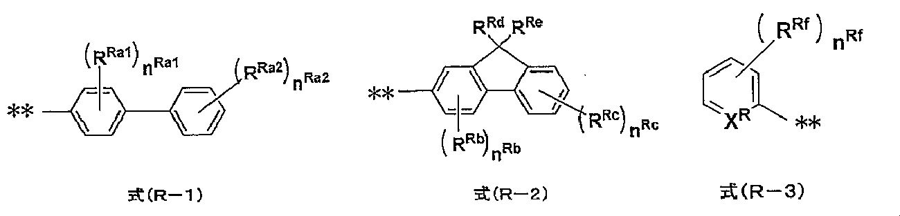
式中、XRはCHまたはNを表す。RRa1、RRa2、RRb、RRcおよびRRfは各々独立に置換基を表す。nRa1、nRcおよびnRfは0~4の整数を表し、nRa2は0~5の整数を表し、nRbは0~3の整数を表す。RRdおよびRReは各々独立にアルキル基を表し、RRdとRReが互いに結合して環を形成してもよい。**は式(D)、式(D-1)~式(D-4)のいずれかの式中のNとの結合位置を表す。
RRa1およびnRa1は後述する式(D-1)におけるRLa1およびnLa1と同義であり、RRb~RReおよびnRbは後述する式(D-2)におけるRLb~RLeおよびnLbと同義である。RRa2およびRRcの置換基としては、上記アリール基、ヘテロアリール基が有してもよい置換基が挙げられる。
本発明において、RRa1、RRa2、RRb、RRcおよびRRfは、各々独立に、置換基TD2であることがさらに好ましい。
RRa1およびnRa1は後述する式(D-1)におけるRLa1およびnLa1と同義であり、RRb~RReおよびnRbは後述する式(D-2)におけるRLb~RLeおよびnLbと同義である。RRa2およびRRcの置換基としては、上記アリール基、ヘテロアリール基が有してもよい置換基が挙げられる。
本発明において、RRa1、RRa2、RRb、RRcおよびRRfは、各々独立に、置換基TD2であることがさらに好ましい。
ArD2~ArD4は、それぞれ、上記式(R-1)~(R-3)のいずれかの式で表される基であってもよい。
上記式(D)で表される化合物、すなわち正孔輸送材料としては、下記式(D-1)~(D-4)のいずれかの式で表される化合物がさらに好ましく、電池性能の安定性の点で、式(D-2)が特に好ましい。

式(D-1)~(D-4)中、ArD1~ArD4は式(D)におけるArD1~ArD4と同義である。RLa1、RLa2、RLbおよびRLcは各々独立に置換基を表す。nLa1およびnLa2は各々独立に0~4の整数を表し、nLbおよびnLcは各々独立に0~3の整数を表す。RLdおよびRLeは各々独立にアルキル基を表し、RLdとRLeが互いに結合して環を形成してもよい。
YおよびZは各々独立にO、Sまたは-CH=N-を表し、Yは-CH=N-が好ましく、ZはSが好ましい。RLg1およびRLg2は各々独立に置換基を表す。RLf1、RLf2、RLh1およびRLh2は各々独立に水素原子または置換基を表す。nLg1およびnLg2は各々独立に0~4の整数を表す。lbは1~4の整数を表す。
YおよびZは各々独立にO、Sまたは-CH=N-を表し、Yは-CH=N-が好ましく、ZはSが好ましい。RLg1およびRLg2は各々独立に置換基を表す。RLf1、RLf2、RLh1およびRLh2は各々独立に水素原子または置換基を表す。nLg1およびnLg2は各々独立に0~4の整数を表す。lbは1~4の整数を表す。
RLa1およびnL1aは式(L-1)におけるRLaおよびnLaと同義であり、好ましい範囲も同じである。RLa2およびnL2aは、対応するRLa1およびnL1aと同義であり、好ましい範囲も同じである。RLb、RLc、nLbおよびnLcは式(L-2)におけるRLb、RLc、nLbおよびnLcと同義である。RLdおよびRLeは式(L-2)におけるRxおよびRyと同義であり、好ましい範囲も同じである。
Yは式(L-3)におけるYと同義であり、好ましい範囲も同じである。Zは式(L-4)におけるZと同義であり、好ましい範囲も同じである。RLf1およびRLf2は(L-3)におけるRLf1およびRLf2と同義であり、好ましい範囲も同じである。RLg1、RLg2、RLh1およびRLh2は式(L-4)におけるRLg1、RLg2、RLh1およびRLh2と同義であり、好ましい範囲も同じである。nLg1およびnLg2は式(L-4)におけるnLg1およびnLg2と同義であり、好ましい範囲も同じである。
Yは式(L-3)におけるYと同義であり、好ましい範囲も同じである。Zは式(L-4)におけるZと同義であり、好ましい範囲も同じである。RLf1およびRLf2は(L-3)におけるRLf1およびRLf2と同義であり、好ましい範囲も同じである。RLg1、RLg2、RLh1およびRLh2は式(L-4)におけるRLg1、RLg2、RLh1およびRLh2と同義であり、好ましい範囲も同じである。nLg1およびnLg2は式(L-4)におけるnLg1およびnLg2と同義であり、好ましい範囲も同じである。
以下に、式(D)で表される化合物の具体例を示すが、これによって本発明が限定されるものではない。
ここで、Meはメチル、Etはエチル、n-Prはn-プロピルを表す。
ここで、Meはメチル、Etはエチル、n-Prはn-プロピルを表す。
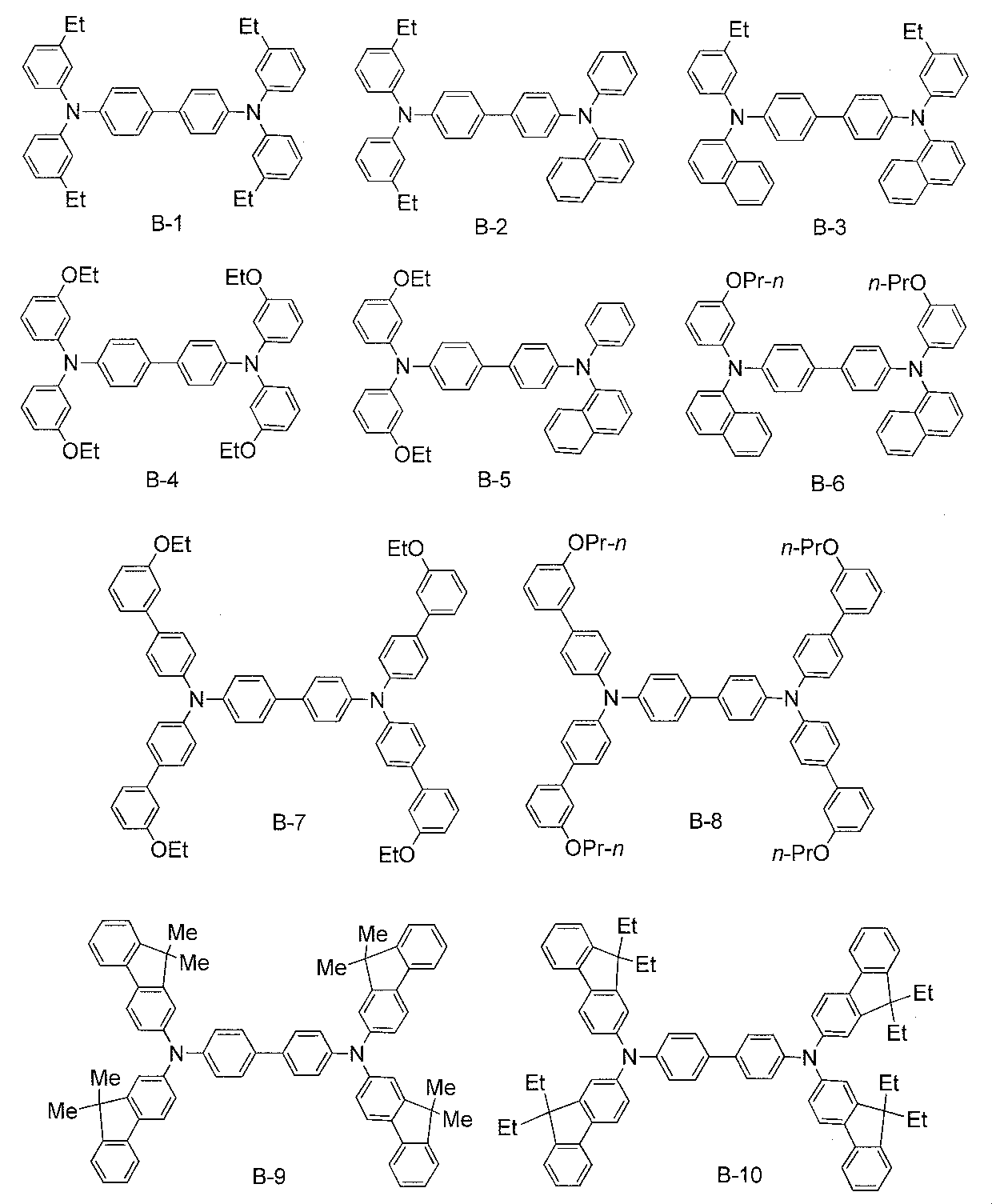
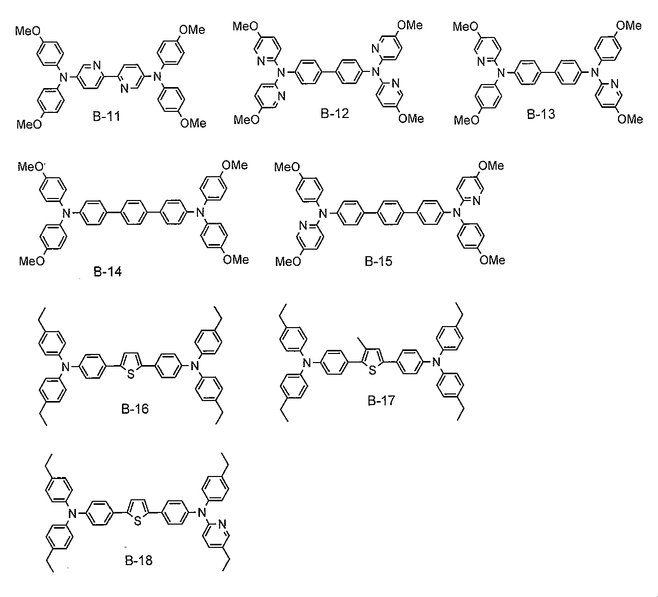

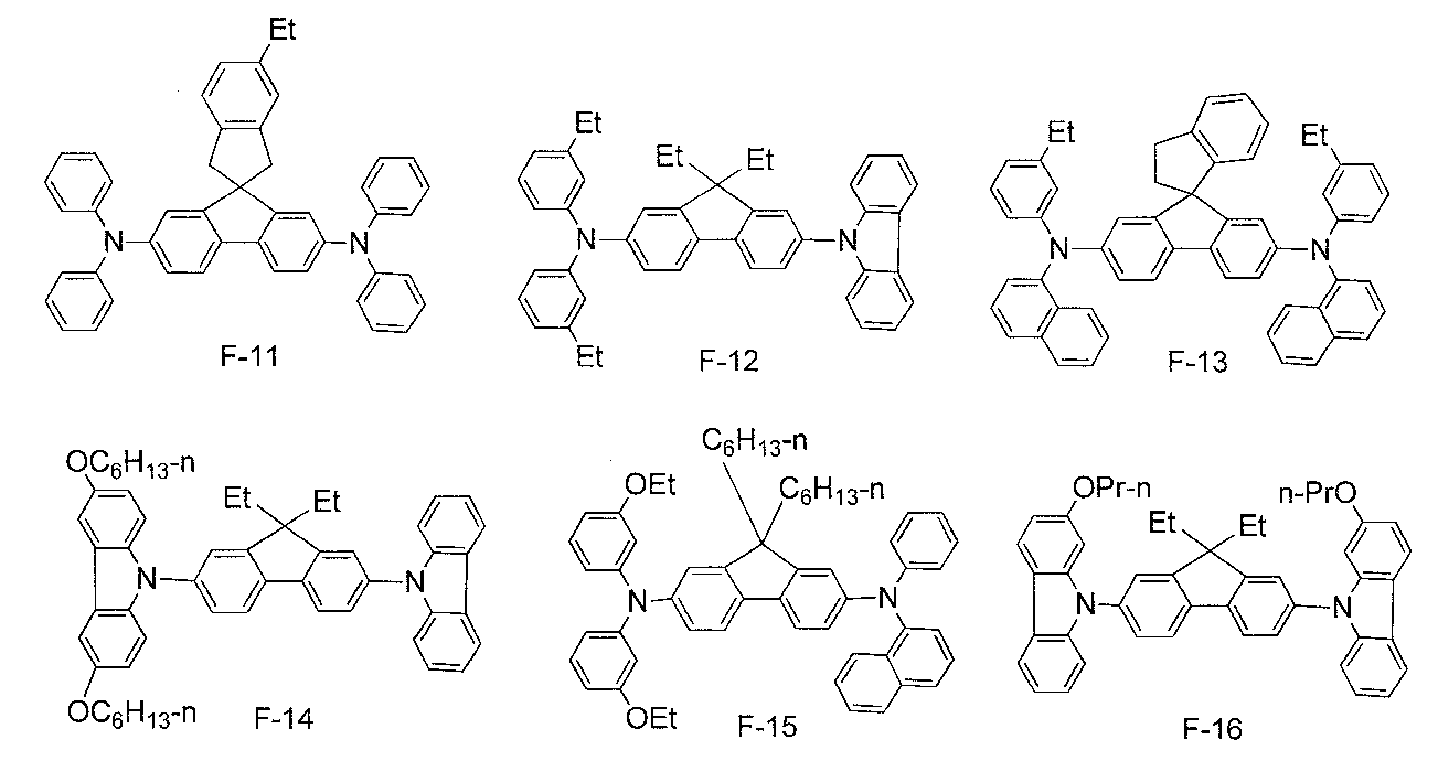

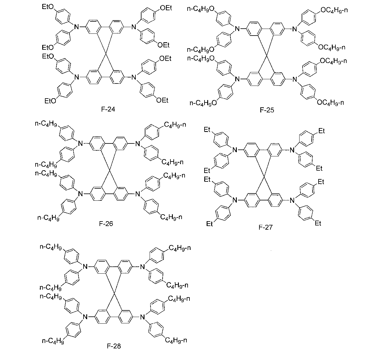
式(D)で表される化合物は、上記に加えて、米国特許第5,061,569号明細書に記載されている2個の縮合芳香族環を分子内に有する、例えば4,4’-ビス[N-(1-ナフチル)-N-フェニルアミノ]ビフェニル(NPDと略記する)、特開平4-308688号公報に記載されているトリフェニルアミンユニットが3つスターバースト型に連結された4,4’,4”-トリス[N-(3-メチルフェニル)-N-フェニルアミノ]トリフェニルアミン(MTDATAと略記する)等を挙げることができる。
式(D)で表される化合物は、Comprehensive Organic Synthesis - Selectivity,Strategy and efficiency in Modern Organic Chemistryに記載の方法に準じて合成することができる。
本発明において、上記HOMOのエネルギー準位が-4.50~-5.00eVの範囲内にある正孔輸送材料と併用できる上記正孔輸送材料としては、例えば、CuI、CuNCS等の無機材料、および、特開2001-291534号公報の段落番号0209~0212に記載の有機正孔輸送材料等が挙げられる。また、有機正孔輸送材料としては、ポリチオフェン〔例えば、ポリ(3-ヘキシルチオフェン-2,5-ジイル)、ポリエチレンジオキシチオフェン(PEDOT)〕や、HOMOのエネルギー準位が-4.50~-5.00eVの範囲外であるポリアニリン、ポリピロールおよびポリシラン等の導電性高分子、2個の環がC、Siなど四面体構造をとる中心原子を共有するスピロ化合物〔例えば、2,2’,7,7’-テトラキス-(N,N-ジ-p-メトキシフェニルアミン)-9,9-スピロビフルオレン(Spiro-OMeTAD)〕、トリアリールアミン等の芳香族アミン化合物(例えば、ポリ(トリフェニルアミン)、4-(ジエチルアミノ)ベンズアルデヒド ジフェニルヒドラゾン)、トリフェニレン化合物、含窒素複素環化合物または液晶性シアノ化合物が挙げられる。
正孔輸送材料は、HOMOのエネルギー準位が-4.50~-5.00eVの範囲内の正孔輸送材料(化合物)のみを含むことが好ましい。正孔輸送材料として、HOMOのエネルギー準位が-4.50~-5.00eVの範囲外の正孔輸送材料を併用する場合、この併用する正孔輸送材料は、使用する正孔輸送材料全てを100質量部とした場合、95質量部以下が好ましく、90質量部以下がより好ましい。
本発明の好ましい態様としての正孔輸送材料は、溶液塗布が可能で、溶解性に優れ、しかも固体状の正孔輸送材料である。
正孔輸送層3の膜厚は、特に限定されないが、50μm以下が好ましく、1nm~10μmがより好ましく、5nm~5μmがさらに好ましく、10nm~1μmが特に好ましい。なお、正孔輸送層3の膜厚は、第二電極2との距離に相当する。この膜厚は、走査型電子顕微鏡(SEM)等を用いて光電変換素子10の断面を観察することにより、測定できる。
本発明において、感光層13と正孔輸送層3との合計膜厚(多孔質層12を有する場合、多孔質層12と感光層13と正孔輸送層3との合計膜厚)は、特に限定されない。合計膜厚は、例えば、0.1~200μmが好ましく、0.5~50μmがより好ましく、0.5~5μmがさらに好ましい。
<第二電極2>
第二電極2は、太陽電池において正極として機能する。第二電極2は、導電性を有していれば特に限定されず、通常、導電性支持体11と同じ構成とすることができる。強度が十分に保たれる場合は、支持体11aは必ずしも必要ではない。
第二電極2の構造としては、集電効果が高い構造が好ましい。感光層13に光が到達するためには、導電性支持体11と第二電極2との少なくとも一方は実質的に透明でなければならない。本発明の太陽電池においては、導電性支持体11が透明であって太陽光を支持体11a側から入射させるのが好ましい。この場合、第二電極2は光を反射する性質を有することがさらに好ましい。
第二電極2は、太陽電池において正極として機能する。第二電極2は、導電性を有していれば特に限定されず、通常、導電性支持体11と同じ構成とすることができる。強度が十分に保たれる場合は、支持体11aは必ずしも必要ではない。
第二電極2の構造としては、集電効果が高い構造が好ましい。感光層13に光が到達するためには、導電性支持体11と第二電極2との少なくとも一方は実質的に透明でなければならない。本発明の太陽電池においては、導電性支持体11が透明であって太陽光を支持体11a側から入射させるのが好ましい。この場合、第二電極2は光を反射する性質を有することがさらに好ましい。
第二電極2を形成する材料としては、例えば、白金(Pt)、金(Au)、ニッケル(Ni)、銅(Cu)、銀(Ag)、インジウム(In)、ルテニウム(Ru)、パラジウム(Pd)、ロジウム(Rh)、イリジウム(Ir)、オスニウム(Os)等の金属、上述の導電性の金属酸化物、炭素材料等が挙げられる。炭素材料としては、炭素原子同士が結合してなる、導電性を有する材料であればよく、例えば、フラーレン、カーボンナノチューブ、グラファイト、グラフェン等が挙げられる。
第二電極2としては、金属もしくは導電性の金属酸化物の薄膜(蒸着してなる薄膜を含む)を有するガラスまたはプラスチックが好ましく、AuもしくはPtの薄膜を有するガラス、または、Ptを蒸着したガラスが特に好ましい。
第二電極2としては、金属もしくは導電性の金属酸化物の薄膜(蒸着してなる薄膜を含む)を有するガラスまたはプラスチックが好ましく、AuもしくはPtの薄膜を有するガラス、または、Ptを蒸着したガラスが特に好ましい。
第二電極2の膜厚は、特に限定されず、0.01~100μmが好ましく、0.01~10μmがさらに好ましく、0.01~1μmが特に好ましい。
<その他の構成>
本発明では、第一電極1と第二電極2との接触を防ぐために、ブロッキング層14に代えて、または、ブロッキング層14とともに、スペーサーやセパレータを用いることもできる。
また、第二電極2と正孔輸送層3の間に正孔ブロッキング層を設けてもよい。
本発明では、第一電極1と第二電極2との接触を防ぐために、ブロッキング層14に代えて、または、ブロッキング層14とともに、スペーサーやセパレータを用いることもできる。
また、第二電極2と正孔輸送層3の間に正孔ブロッキング層を設けてもよい。
<<太陽電池>>
本発明の太陽電池は、例えば図1~図3に示されるように、光電変換素子10を外部回路6に対して仕事させるように構成したものである。第一電極1(導電性支持体11)および第二電極2に接続される外部回路は、公知のものを特に制限されることなく、用いることができる。
本発明の太陽電池は、構成物の劣化および蒸散等を防止するために、側面をポリマーや接着剤等で密封することが好ましい。
本発明の光電変換素子が適用される太陽電池は、特に限定されず、例えば特許文献1、非特許文献1~3に記載の太陽電池が挙げられる。
本発明の太陽電池は、例えば図1~図3に示されるように、光電変換素子10を外部回路6に対して仕事させるように構成したものである。第一電極1(導電性支持体11)および第二電極2に接続される外部回路は、公知のものを特に制限されることなく、用いることができる。
本発明の太陽電池は、構成物の劣化および蒸散等を防止するために、側面をポリマーや接着剤等で密封することが好ましい。
本発明の光電変換素子が適用される太陽電池は、特に限定されず、例えば特許文献1、非特許文献1~3に記載の太陽電池が挙げられる。
<<光電変換素子および太陽電池の製造方法>>
本発明の実施形態にかかる光電変換素子および太陽電池は、公知の製造方法、例えば非特許文献1~3等に記載の方法等に準拠して、製造できる。
以下に、本発明の実施形態にかかる光電変換素子および太陽電池の製造方法を簡単に説明する。
本発明の実施形態にかかる光電変換素子および太陽電池は、公知の製造方法、例えば非特許文献1~3等に記載の方法等に準拠して、製造できる。
以下に、本発明の実施形態にかかる光電変換素子および太陽電池の製造方法を簡単に説明する。
導電性支持体11の表面に、所望により、ブロッキング層14および多孔質層12の少なくとも一方を成膜する。
ブロッキング層14は、例えば、上記絶縁性物質またはその前駆体化合物等を含有する分散物を導電性支持体11の表面に塗布し、焼成する方法またはスプレー熱分解法等によって、成膜できる。
ブロッキング層14は、例えば、上記絶縁性物質またはその前駆体化合物等を含有する分散物を導電性支持体11の表面に塗布し、焼成する方法またはスプレー熱分解法等によって、成膜できる。
多孔質層12を形成する材料は、好ましくは微粒子として用いられ、さらに好ましくは微粒子を含有する分散物として用いられる。
多孔質層12を成膜する方法としては、特に限定されず、例えば、湿式法、乾式法、その他の方法(例えば、Chemical Review,第110巻,6595頁(2010年刊)に記載の方法)が挙げられる。これらの方法において、導電性支持体11の表面またはブロッキング層14の表面に分散物(ペースト)を塗布した後に、100~800℃の温度で10分~10時間焼成することが好ましい。これにより、微粒子同士を密着させることができる。
焼成を複数回行う場合、最後の焼成以外の焼成の温度(最後以外の焼成温度)を、最後の焼成の温度(最後の焼成温度)よりも低い温度で行うのがよい。例えば、酸化チタンペーストを用いる場合、最後以外の焼成温度を50~300℃の範囲内に設定することができる。また、最後の焼成温度を、100~600℃の範囲内において、最後以外の焼成温度よりも高くなるように、設定することができる。支持体11aとしてガラス支持体を用いる場合、焼成温度は60~500℃が好ましい。
多孔質層12を成膜する方法としては、特に限定されず、例えば、湿式法、乾式法、その他の方法(例えば、Chemical Review,第110巻,6595頁(2010年刊)に記載の方法)が挙げられる。これらの方法において、導電性支持体11の表面またはブロッキング層14の表面に分散物(ペースト)を塗布した後に、100~800℃の温度で10分~10時間焼成することが好ましい。これにより、微粒子同士を密着させることができる。
焼成を複数回行う場合、最後の焼成以外の焼成の温度(最後以外の焼成温度)を、最後の焼成の温度(最後の焼成温度)よりも低い温度で行うのがよい。例えば、酸化チタンペーストを用いる場合、最後以外の焼成温度を50~300℃の範囲内に設定することができる。また、最後の焼成温度を、100~600℃の範囲内において、最後以外の焼成温度よりも高くなるように、設定することができる。支持体11aとしてガラス支持体を用いる場合、焼成温度は60~500℃が好ましい。
多孔質層12を成膜するときの、多孔質材料の塗布量は、成膜する多孔質層12の膜厚および塗布回数等に応じて適宜に設定され、特に限定されない。導電性支持体11の表面積1m2当たりの多孔質材料の塗布量は、例えば、0.5~500gが好ましく、さらには5~100gが好ましい。
次いで、感光層13を設ける。
まず、感光層13を形成するための光吸収剤溶液を調製する。光吸収剤溶液は、上記ペロブスカイト化合物の原料であるMX2とAXとを含有する。ここで、A、MおよびXは上記式(I)のA、MおよびXと同義である。この光吸収剤溶液において、ペロブスカイト化合物(P)のa等に応じて、MX2とAXとのモル比が調整される。
次いで、調製した光吸収剤溶液を、多孔質層12の表面またはブロッキング層14の表面に塗布し、乾燥する。これにより、ペロブスカイト化合物が多孔質層12の表面またはブロッキング層14の表面に形成される。
これにより、ペロブスカイト化合物が多孔質層12の表面またはブロッキング層14の表面に形成される。
まず、感光層13を形成するための光吸収剤溶液を調製する。光吸収剤溶液は、上記ペロブスカイト化合物の原料であるMX2とAXとを含有する。ここで、A、MおよびXは上記式(I)のA、MおよびXと同義である。この光吸収剤溶液において、ペロブスカイト化合物(P)のa等に応じて、MX2とAXとのモル比が調整される。
次いで、調製した光吸収剤溶液を、多孔質層12の表面またはブロッキング層14の表面に塗布し、乾燥する。これにより、ペロブスカイト化合物が多孔質層12の表面またはブロッキング層14の表面に形成される。
これにより、ペロブスカイト化合物が多孔質層12の表面またはブロッキング層14の表面に形成される。
このようにして設けられた感光層13上に正孔輸送材料を含有する正孔輸送材料溶液を塗布し、乾燥して正孔輸送層3を成膜する。
正孔輸送材料溶液は、塗布性に優れる点、および多孔質層12を有する場合は多孔質層12の孔内部まで侵入しやすい点で、正孔輸送材料の濃度が0.1~1.0M(モル/L)であるのが好ましい。
正孔輸送材料溶液は、塗布性に優れる点、および多孔質層12を有する場合は多孔質層12の孔内部まで侵入しやすい点で、正孔輸送材料の濃度が0.1~1.0M(モル/L)であるのが好ましい。
正孔輸送層3を成膜した後に第二電極2を形成して、光電変換素子および太陽電池が製造される。
各層の膜厚は、各分散液または溶液の濃度、塗布回数を適宜に変更して、調整できる。例えば、図2または図3に示す膜厚が厚い感光層13Bを設ける場合には、分散液を複数回塗布、乾燥すればよい。
上述の各分散液および溶液は、それぞれ、必要に応じて、分散助剤、界面活性剤等の添加剤を含有していてもよい。
光電変換素子および太陽電池の製造方法に使用する溶媒または分散媒としては、特開2001-291534号公報に記載の溶媒が挙げられるが、特にこれに限定されない。本発明においては、有機溶媒が好ましく、さらにアルコール溶媒、アミド溶媒、ニトリル溶媒、炭化水素溶媒、ラクトン溶媒、および、これらの2種以上の混合溶媒がより好ましい。混合溶媒としては、アルコール溶媒と、アミド溶媒、ニトリル溶媒または炭化水素溶媒から選ばれる溶媒との混合溶媒が好ましい。具体的には、メタノール、エタノール、γ-ブチロラクトン、クロロベンゼン、アセトニトリル、ジメチルホルムアミド(DMF)もしくはジメチルアセトアミド、または、これらの混合溶媒が好ましい。
各層を形成する溶液または分散剤の塗布方法は、特に限定されず、スピンコート、エクストルージョンダイコート、ブレードコート、バーコート、スクリーン印刷、ステンシル印刷、ロールコート、カーテンコート、スプレーコート、ディップコート、インクジェット印刷法、浸漬法等、公知の塗布方法を用いることができる。なかでも、スピンコート、スクリーン印刷、浸漬法等が好ましい。
太陽電池は、上記のようにして作製した光電変換素子の第一電極1および第二電極2に外部回路を接続して、製造される。
以下に実施例に基づき、本発明についてさらに詳細に説明するが、本発明はこれに限定されない。
実施例1
以下に示す手順により、図1に示される光電変換素子10Aおよび太陽電池を製造した。なお、感光層13の膜厚が大きい場合は、図2に示される光電変換素子10Bおよび太陽電池に対応することになる。
以下に示す手順により、図1に示される光電変換素子10Aおよび太陽電池を製造した。なお、感光層13の膜厚が大きい場合は、図2に示される光電変換素子10Bおよび太陽電池に対応することになる。
<ブロッキング層用溶液の調製>
チタニウム ジイソプロポキシド ビス(アセチルアセトナート)の15質量%イソプロパノール溶液(アルドリッチ社製)を1-ブタノールで希釈して、0.02Mのブロッキング層用溶液を調製した。
チタニウム ジイソプロポキシド ビス(アセチルアセトナート)の15質量%イソプロパノール溶液(アルドリッチ社製)を1-ブタノールで希釈して、0.02Mのブロッキング層用溶液を調製した。
<ブロッキング層14の成膜>
ガラス基板(支持体11a、厚さ2.2mm)上にフッ素ドープされたSnO2導電膜(透明電極11b)を形成し、導電性支持体11を作製した。調製した0.02Mのブロッキング層用溶液を用いてスプレー熱分解法により、450℃にて、上記SnO2導電膜上にブロッキング層14(膜厚100nm)を成膜した。
ガラス基板(支持体11a、厚さ2.2mm)上にフッ素ドープされたSnO2導電膜(透明電極11b)を形成し、導電性支持体11を作製した。調製した0.02Mのブロッキング層用溶液を用いてスプレー熱分解法により、450℃にて、上記SnO2導電膜上にブロッキング層14(膜厚100nm)を成膜した。
<酸化チタンペーストの調製>
酸化チタン(アナターゼ、平均粒径20nm)のエタノール分散液に、エチルセルロース、ラウリン酸およびテルピネオールを加えて、酸化チタンペーストを調製した。
酸化チタン(アナターゼ、平均粒径20nm)のエタノール分散液に、エチルセルロース、ラウリン酸およびテルピネオールを加えて、酸化チタンペーストを調製した。
<多孔質層12の形成>
調製した酸化チタンペーストをブロッキング層14の上にスクリーン印刷法で塗布し、焼成した。この酸化チタンペーストの塗布および焼成をそれぞれ2回行った。焼成温度は、1回目の焼成を130℃で行い、2回目の焼成を500℃で1時間行った。得られた酸化チタンの焼成体を、40mMのTiCl4水溶液に浸した後、60℃で1時間、続けて500℃で30分間加熱して、TiO2からなる多孔質層12(膜厚500nm)を成膜した。
調製した酸化チタンペーストをブロッキング層14の上にスクリーン印刷法で塗布し、焼成した。この酸化チタンペーストの塗布および焼成をそれぞれ2回行った。焼成温度は、1回目の焼成を130℃で行い、2回目の焼成を500℃で1時間行った。得られた酸化チタンの焼成体を、40mMのTiCl4水溶液に浸した後、60℃で1時間、続けて500℃で30分間加熱して、TiO2からなる多孔質層12(膜厚500nm)を成膜した。
<感光層13Aの形成>
上記のようにして成膜した多孔質層12の上に下記感光層A~Cのいずれかの感光層を以下のようにして形成し、第一電極1を作製した。
(感光層Aの形成)
メチルアミンの40%メタノール溶液(27.86mL)と57質量%のヨウ化水素の水溶液(ヨウ化水素酸、30mL)を、フラスコ中、0℃で2時間攪拌した後、濃縮して、CH3NH3Iの粗体を得た。得られた粗体CH3NH3Iをエタノールに溶解し、ジエチルエーテルで再結晶した。析出した結晶をろ取し、60℃で24時間減圧乾燥して、精製CH3NH3Iを得た。
次いで、精製CH3NH3IとPbI2を、モル比で2:1とし、γ-ブチロラクトン中、60℃で12時間攪拌して混合した後、ポリテトラフルオロエチレン(PTFE)シリンジフィルターでろ過して、40質量%の光吸収剤溶液Aを調製した。
上記のようにして成膜した多孔質層12の上に下記感光層A~Cのいずれかの感光層を以下のようにして形成し、第一電極1を作製した。
(感光層Aの形成)
メチルアミンの40%メタノール溶液(27.86mL)と57質量%のヨウ化水素の水溶液(ヨウ化水素酸、30mL)を、フラスコ中、0℃で2時間攪拌した後、濃縮して、CH3NH3Iの粗体を得た。得られた粗体CH3NH3Iをエタノールに溶解し、ジエチルエーテルで再結晶した。析出した結晶をろ取し、60℃で24時間減圧乾燥して、精製CH3NH3Iを得た。
次いで、精製CH3NH3IとPbI2を、モル比で2:1とし、γ-ブチロラクトン中、60℃で12時間攪拌して混合した後、ポリテトラフルオロエチレン(PTFE)シリンジフィルターでろ過して、40質量%の光吸収剤溶液Aを調製した。
調製した光吸収剤溶液Aをスピンコート法(2000rpmで60秒、続けて3000rpmで60秒)により多孔質層12の上に塗布し、塗布した光吸収剤溶液Aをホットプレートにより100℃で40分間乾燥して、ペロブスカイト化合物を有する感光層13Aとしての感光層A(膜厚600nm)を形成した。得られたペロブスカイト化合物はCH3NH3PbI3であった。
(感光層Bの形成)
ホルムアミジン酢酸塩と、ホルムアミジン酢酸塩に対して2当量のヨウ化水素を含む57質量%のヨウ化水素の水溶液とを、フラスコ中、0℃で1時間攪拌し、次いで、50℃に昇温し、さらに1時間攪拌し、混合した。得られた溶液を濃縮して、ホルムアミジン・ヨウ化水素塩の粗体を得た。得られた粗体をジエチルエーテルで再結晶し、析出した結晶をろ取し、50℃で10時間減圧乾燥して、精製ホルムアミジン・ヨウ化水素塩を得た。
次いで、精製ホルムアミジン・ヨウ化水素塩とPbI2を、モル比で2:1とし、ジメチルホルムアミド(DMF)中、60℃で3時間攪拌して混合した後、ポリテトラフルオロエチレン(PTFE)シリンジフィルターでろ過して、40質量%の光吸収剤溶液Bを調製した。
ホルムアミジン酢酸塩と、ホルムアミジン酢酸塩に対して2当量のヨウ化水素を含む57質量%のヨウ化水素の水溶液とを、フラスコ中、0℃で1時間攪拌し、次いで、50℃に昇温し、さらに1時間攪拌し、混合した。得られた溶液を濃縮して、ホルムアミジン・ヨウ化水素塩の粗体を得た。得られた粗体をジエチルエーテルで再結晶し、析出した結晶をろ取し、50℃で10時間減圧乾燥して、精製ホルムアミジン・ヨウ化水素塩を得た。
次いで、精製ホルムアミジン・ヨウ化水素塩とPbI2を、モル比で2:1とし、ジメチルホルムアミド(DMF)中、60℃で3時間攪拌して混合した後、ポリテトラフルオロエチレン(PTFE)シリンジフィルターでろ過して、40質量%の光吸収剤溶液Bを調製した。
調製した光吸収剤溶液Bをスピンコート法(2000rpmで60秒、続けて3000rpmで60秒)により多孔質層12の上に塗布した。塗布した光吸収剤溶液Bをホットプレートにより160℃で40分間乾燥して、ペロブスカイト化合物を有する感光層13Aとしての感光層Bを形成した。得られたペロブスカイト化合物はCH(=NH)NH3PbI3であった。
(感光層Cの形成)
エチルアミンの40%エタノール溶液と57質量%のヨウ化水素の水溶液とを、フラスコ中、0℃で2時間攪拌した後、濃縮して、CH3CH2NH3Iの粗体を得た。得られた粗体をエタノールに溶解し、ジエチルエーテルで再結晶した。析出した結晶をろ取し、60℃で12時間減圧乾燥して、精製CH3CH2NH3Iを得た。
次いで、精製CH3CH2NH3IとPbI2を、モル比で3:1とし、ジメチルホルムアミド(DMF)中、60℃で5時間攪拌して混合した後、ポリテトラフルオロエチレン(PTFE)シリンジフィルターでろ過して、40質量%の光吸収剤溶液Cを調製した。
エチルアミンの40%エタノール溶液と57質量%のヨウ化水素の水溶液とを、フラスコ中、0℃で2時間攪拌した後、濃縮して、CH3CH2NH3Iの粗体を得た。得られた粗体をエタノールに溶解し、ジエチルエーテルで再結晶した。析出した結晶をろ取し、60℃で12時間減圧乾燥して、精製CH3CH2NH3Iを得た。
次いで、精製CH3CH2NH3IとPbI2を、モル比で3:1とし、ジメチルホルムアミド(DMF)中、60℃で5時間攪拌して混合した後、ポリテトラフルオロエチレン(PTFE)シリンジフィルターでろ過して、40質量%の光吸収剤溶液Cを調製した。
調製した光吸収剤溶液Cをスピンコート法(2000rpmで60秒、続けて3000rpmで60秒)により多孔質層12の上に塗布した。塗布した光吸収剤溶液Cをホットプレートにより140℃で40分間乾燥して、ペロブスカイト化合物を有する感光層13Aとしての感光層Cを形成した。得られたペロブスカイト化合物は(CH3CH2-NH3)2PbI4であった。
<正孔輸送材料溶液の調製>
下記表1に記載の正孔輸送材料(180mg)をクロロベンゼン(1mL)に溶解した。このクロロベンゼン溶液に、リチウム-ビス(トリフルオロメタンスルホニル)イミド(170mg)をアセトニトリル(1mL)に溶解させたアセトニトリル溶液(37.5μL)と、t-ブチルピリジン(TBP、17.5μL)とを加えて混合し、正孔輸送材料溶液を調製した。
下記表1に記載の正孔輸送材料(180mg)をクロロベンゼン(1mL)に溶解した。このクロロベンゼン溶液に、リチウム-ビス(トリフルオロメタンスルホニル)イミド(170mg)をアセトニトリル(1mL)に溶解させたアセトニトリル溶液(37.5μL)と、t-ブチルピリジン(TBP、17.5μL)とを加えて混合し、正孔輸送材料溶液を調製した。
<正孔輸送層3の成膜>
次いで調製した正孔輸送材料溶液を、スピンコート法により、第一電極1の感光層13上に塗布し、塗布した正孔輸送材料溶液を乾燥して、正孔輸送層3(膜厚0.5μm)を成膜した。
次いで調製した正孔輸送材料溶液を、スピンコート法により、第一電極1の感光層13上に塗布し、塗布した正孔輸送材料溶液を乾燥して、正孔輸送層3(膜厚0.5μm)を成膜した。
<第二電極2の作製>
蒸着法により金を正孔輸送層3上に蒸着して、第二電極2(膜厚0.3μm)を作製した。
表1に記載された、感光層および正孔輸送材料を用いた以外は同様にして、光電変換素子および太陽電池(試料No.101~125、201及び202)を製造した。
蒸着法により金を正孔輸送層3上に蒸着して、第二電極2(膜厚0.3μm)を作製した。
表1に記載された、感光層および正孔輸送材料を用いた以外は同様にして、光電変換素子および太陽電池(試料No.101~125、201及び202)を製造した。
ここで、上記の各膜厚は、上記方法に従って、SEMで観察し、観測範囲内の10区分の平均を求め、この値を膜厚とした。
上記のようにして製造した各太陽電池の下記性能を、以下のようにして、評価した。
なお、正孔輸送材料のDFT計算によるHOMOのエネルギー準位は、Gaussian09により、汎関数としてB3LYP、基底関数として3-21Gを用いて計算した。
なお、正孔輸送材料のDFT計算によるHOMOのエネルギー準位は、Gaussian09により、汎関数としてB3LYP、基底関数として3-21Gを用いて計算した。
<太陽電池の評価>
上記のようにして製造した太陽電池それぞれを用いて電池特性試験を行った。この試験により、各太陽電池の短絡電流密度(Jsc:単位mA/cm2)、開放電圧(Voc:単位V)およびフィルファクター(FF)を求め、電池出力を入射エネルギーで除することにより、光電変換効率〔η(%)〕を算出した。
電池特性試験は、ソーラーシミュレーター「PEC-L12」(ペクセル・テクノロジーズ社製)を用いて、行った。特性評価は、I-V特性計測装置「PECK2400-N」(ペクセル・テクノロジーズ社製)を用いて、行った。
上記のようにして製造した太陽電池それぞれを用いて電池特性試験を行った。この試験により、各太陽電池の短絡電流密度(Jsc:単位mA/cm2)、開放電圧(Voc:単位V)およびフィルファクター(FF)を求め、電池出力を入射エネルギーで除することにより、光電変換効率〔η(%)〕を算出した。
電池特性試験は、ソーラーシミュレーター「PEC-L12」(ペクセル・テクノロジーズ社製)を用いて、行った。特性評価は、I-V特性計測装置「PECK2400-N」(ペクセル・テクノロジーズ社製)を用いて、行った。
(初期性能の評価)
初期性能の評価を、初期変換効率により、評価した。具体的には、各試料番号の太陽電池を同一条件で5個製造し、得られた5個の太陽電池の光電変換効率を上記のようにして算出し、これらの平均値を求めた。求めた平均値を各試料番号の太陽電池の初期変換効率とした。
このようにして得られた初期変換効率により、初期性能を下記の評価基準で評価した。
本発明において、初期性能の評価は、A、B+およびBであることが求められ、実用上、好ましくはAである。
初期性能の評価を、初期変換効率により、評価した。具体的には、各試料番号の太陽電池を同一条件で5個製造し、得られた5個の太陽電池の光電変換効率を上記のようにして算出し、これらの平均値を求めた。求めた平均値を各試料番号の太陽電池の初期変換効率とした。
このようにして得られた初期変換効率により、初期性能を下記の評価基準で評価した。
本発明において、初期性能の評価は、A、B+およびBであることが求められ、実用上、好ましくはAである。
A:初期変換効率が下記比較化合物R-2の初期変換効率に対して1.3倍以上のもの
B+:初期変換効率が下記比較化合物R-2の初期変換効率に対して1.2倍以上1.3倍未満のもの
B:初期変換効率が下記比較化合物R-2の初期変換効率に対して1.1倍以上1.2倍未満のもの
C:初期変換効率が下記比較化合物R-2の初期変換効率に対して1.1倍未満のもの
B+:初期変換効率が下記比較化合物R-2の初期変換効率に対して1.2倍以上1.3倍未満のもの
B:初期変換効率が下記比較化合物R-2の初期変換効率に対して1.1倍以上1.2倍未満のもの
C:初期変換効率が下記比較化合物R-2の初期変換効率に対して1.1倍未満のもの
(初期性能のバラツキの評価)
初期性能のバラツキの評価を、初期変換効率のばらつきにより、評価した。具体的には、各試料番号の太陽電池において、5個の太陽電池の初期変換効率の標準偏差を求めた。
このようにして得られた初期変換効率の標準偏差値により、初期性能のバラツキを下記の評価基準で評価した。
本発明において、初期性能のバラツキの評価は、A、B+およびBであることが求められ、実用上、好ましくはAである。
初期性能のバラツキの評価を、初期変換効率のばらつきにより、評価した。具体的には、各試料番号の太陽電池において、5個の太陽電池の初期変換効率の標準偏差を求めた。
このようにして得られた初期変換効率の標準偏差値により、初期性能のバラツキを下記の評価基準で評価した。
本発明において、初期性能のバラツキの評価は、A、B+およびBであることが求められ、実用上、好ましくはAである。
A:初期変換効率の標準偏差値が下記の比較化合物R-2の初期変換効率の標準偏差値に対して0.1倍未満のもの
B+:初期変換効率の標準偏差値が下記の比較化合物R-2の初期変換効率の標準偏差値に対して0.1倍以上0.2倍未満のもの
B:初期変換効率の標準偏差値が下記の比較化合物R-2の初期変換効率の標準偏差値に対して0.2倍以上0.3倍未満のもの
C:初期変換効率の標準偏差値が下記の比較化合物R-2の初期変換効率の標準偏差値に対して0.3倍以上のもの
B+:初期変換効率の標準偏差値が下記の比較化合物R-2の初期変換効率の標準偏差値に対して0.1倍以上0.2倍未満のもの
B:初期変換効率の標準偏差値が下記の比較化合物R-2の初期変換効率の標準偏差値に対して0.2倍以上0.3倍未満のもの
C:初期変換効率の標準偏差値が下記の比較化合物R-2の初期変換効率の標準偏差値に対して0.3倍以上のもの
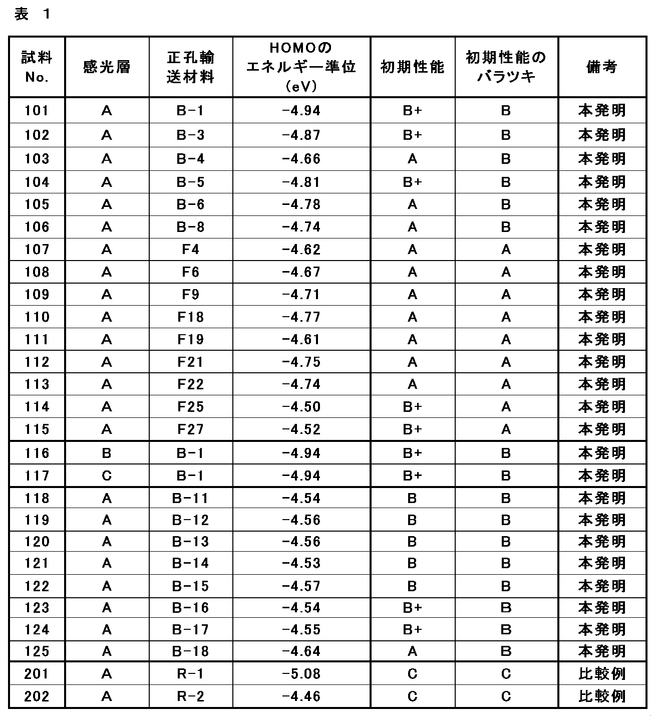
上記試料No.201および202に用いた正孔輸送材料は下記構造の化合物である。
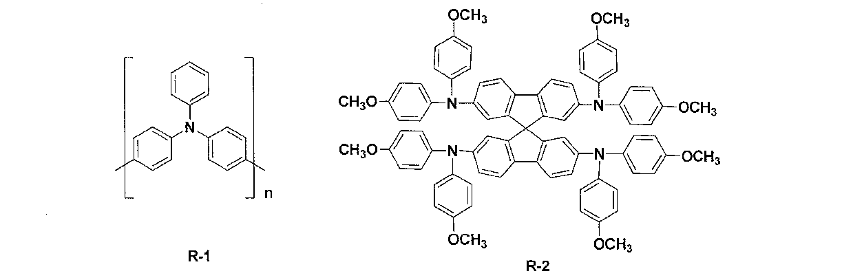
上記表1の結果から明らかなように、試料No.101~125の太陽電池は、いずれも光電変換効率が高く、しかも製造における性能のバラツキが少ないことがわかる。
ペロブスカイト化合物を光吸収剤として含む感光層を備えた太陽電池において、DFT計算によるHOMOのエネルギー準位が-4.50~-5.00eVの範囲内にある正孔輸送材料を用いて正孔輸送層を形成することにより、開放電圧(Voc)を最大限大きくすることが可能になったと考えられる。この結果、本発明の太陽電池は、光電変換効率が向上し、しかも、繰返し製造しても電池性能のバラツキが少なく、安定した電池性能を発揮できる。
また、HOMOのエネルギー準位が-4.60~-4.80eVの範囲内にある正孔輸送材料を用いると(試料No.103、105~113および125)、光電変換効率の向上効果がより高くなることが分かる。上記式(D)のArD1が置換基TD2を有していると(試料No.101~109、111~117および123~125)、光電変換効率の向上効果がより高くなることが分かる。特に、HOMOのエネルギー準位が-4.60~-4.80eVの範囲内で、しかも上記式(D)のArD1が置換基TD2を有していると(試料No.103、105~109、111~113、125)、光電変換効率の向上効果がさらに高くなることが分かる。 上記式(D)のLD1が上記式(L-2)で表される正孔輸送材料を用いると(試料No.107~115)、初期性能のバラツキの抑制効果がより高くなることが分かる。
また、本発明の太陽電池は、光吸収剤として、式(I-1)で表される化合物であっても、また式(I-2)で表される化合物であっても、上記の正孔輸送材料とともに用いられることにより(試料No.101、116および117)、光電変換効率が向上し、電池性能を安定して発揮できることが分かる。
ペロブスカイト化合物を光吸収剤として含む感光層を備えた太陽電池において、DFT計算によるHOMOのエネルギー準位が-4.50~-5.00eVの範囲内にある正孔輸送材料を用いて正孔輸送層を形成することにより、開放電圧(Voc)を最大限大きくすることが可能になったと考えられる。この結果、本発明の太陽電池は、光電変換効率が向上し、しかも、繰返し製造しても電池性能のバラツキが少なく、安定した電池性能を発揮できる。
また、HOMOのエネルギー準位が-4.60~-4.80eVの範囲内にある正孔輸送材料を用いると(試料No.103、105~113および125)、光電変換効率の向上効果がより高くなることが分かる。上記式(D)のArD1が置換基TD2を有していると(試料No.101~109、111~117および123~125)、光電変換効率の向上効果がより高くなることが分かる。特に、HOMOのエネルギー準位が-4.60~-4.80eVの範囲内で、しかも上記式(D)のArD1が置換基TD2を有していると(試料No.103、105~109、111~113、125)、光電変換効率の向上効果がさらに高くなることが分かる。 上記式(D)のLD1が上記式(L-2)で表される正孔輸送材料を用いると(試料No.107~115)、初期性能のバラツキの抑制効果がより高くなることが分かる。
また、本発明の太陽電池は、光吸収剤として、式(I-1)で表される化合物であっても、また式(I-2)で表される化合物であっても、上記の正孔輸送材料とともに用いられることにより(試料No.101、116および117)、光電変換効率が向上し、電池性能を安定して発揮できることが分かる。
1A、1B、1C 第一電極
11 導電性支持体
11a 支持体
11b 透明電極
12 多孔質層
13A、13B、13C 感光層
14 ブロッキング層
2 第二電極
3A、3B、3C 正孔輸送層
6 外部回路(リード)
10A、10B、10C 光電変換素子
100A、100B、100C 光電変換素子を電池用途に応用したシステム
M 電動モーター
11 導電性支持体
11a 支持体
11b 透明電極
12 多孔質層
13A、13B、13C 感光層
14 ブロッキング層
2 第二電極
3A、3B、3C 正孔輸送層
6 外部回路(リード)
10A、10B、10C 光電変換素子
100A、100B、100C 光電変換素子を電池用途に応用したシステム
M 電動モーター
Claims (17)
- 光吸収剤を含む感光層を導電性支持体上に有する第一電極と、該第一電極に対向する第二電極と、該第一電極と該第二電極の間に設けられた正孔輸送層とを有する光電変換素子であって、
前記光吸収剤が、周期表第一族元素もしくはカチオン性有機基Aのカチオンと、前記周期表第一族元素以外の金属原子Mのカチオンと、アニオン性原子Xのアニオンと、を有するペロブスカイト型結晶構造を持つ化合物を含み、
前記正孔輸送層が、密度汎関数理論計算による最高被占軌道のエネルギー準位が-4.50~-5.00eVの範囲内である正孔輸送材料を含有する光電変換素子。
- 前記正孔輸送材料が、下記式(D)で表される請求項1に記載の光電変換素子。

- 前記ArD1~ArD4の少なくとも1つが置換基を有し、該置換基が、1)炭素数2以上の、アルキル基、アルコキシ基、アルキルチオ基、アルキルアミノ基、ジアルキルアミノ基、アルコキシカルボニル基、アルキルシリル基またはアシル基であるか、または、2)該1)に記載の基が置換したアリール基もしくはヘテロアリール基である請求項2に記載の光電変換素子。
- 前記ArD1~ArD4の少なくとも1つが置換基を有し、該置換基が、炭素数2以上のアルキル基、炭素数2以上のアルコキシ基、炭素数2以上のアルキル基が置換したアリール基、炭素数2以上のアルコキシ基が置換したアリール基、炭素数2以上のアルキル基が置換したヘテロアリール基、または、炭素数2以上のアルコキシ基が置換したヘテロアリール基である請求項2または3に記載の光電変換素子。
- 前記LD1が、下記式(L-1)~(L-4)のいずれかの式で表される請求項2~4のいずれか1項に記載の光電変換素子。
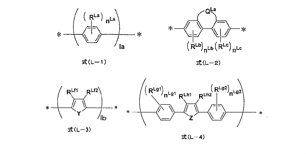
- 前記正孔輸送材料が、下記式(D-1)~(D-4)のいずれかの式で表される請求項2~5のいずれか1項に記載の光電変換素子。
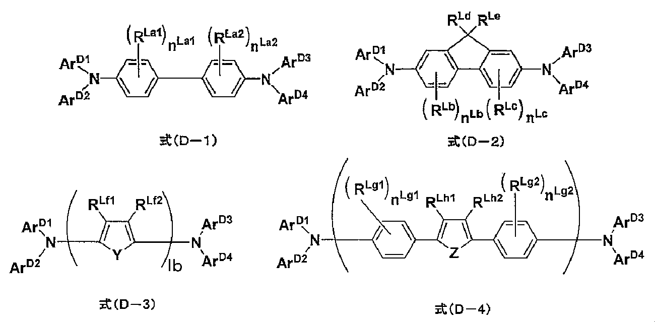
- 前記ArD1が、下記式(R-1)~(R-3)のいずれかの式で表される請求項2~6のいずれか1項に記載の光電変換素子。
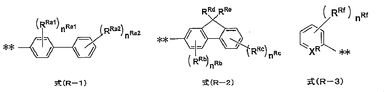
- 前記最高被占軌道のエネルギー準位が、-4.60~-4.80eVの範囲内である請求項1~7のいずれか1項に記載の光電変換素子。
- 前記ペロブスカイト型結晶構造を持つ化合物が、下記式(I)で表される化合物である請求項1~8のいずれか1項に記載の光電変換素子。
式(I):AaMmXx
式(I)中、Aは周期表第一族元素またはカチオン性有機基を表す。Mは周期表第一族元素以外の金属原子を表す。Xはアニオン性原子を表す。aは1または2を表し、mは1を表し、a、mおよびxはa+2m=xを満たす。
- 前記ペロブスカイト型結晶構造を持つ化合物が、下記式(I-1)で表される化合物を含む請求項1~9のいずれか1項に記載の光電変換素子。
式(I-1):AMX3
式(I-1)中、Aは周期表第一族元素またはカチオン性有機基を表す。Mは周期表第一族元素以外の金属原子を表す。Xはアニオン性原子を表す。
- 前記ペロブスカイト型結晶構造を持つ化合物が、下記式(I-2)で表される化合物を含む請求項1~10のいずれか1項に記載の光電変換素子。
式(I-2):A2MX4
式(I-2)中、Aは周期表第一族元素またはカチオン性有機基を表す。Mは周期表第一族元素以外の金属原子を表す。Xはアニオン性原子を表す。
- 前記Aが、下記一般式(1)で表される請求項1~11のいずれか1項に記載の光電変換素子。
式(1):R1a-NH3
式(1)中、R1aは置換基を表す。
- 前記R1aが、アルキル基、シクロアルキル基、アルケニル基、アルキニル基、アリール基、ヘテロアリール基または下記式(2)で表される基である請求項12に記載の光電変換素子。

- 前記Xが、ハロゲン原子である請求項1~13のいずれか1項に記載の光電変換素子。
- 前記Mが、PbまたはSnである請求項1~14のいずれか1項に記載の光電変換素子。
- 前記導電性支持体と前記感光層との間に多孔質層を有する請求項1~15のいずれか1項に記載の光電変換素子。
- 請求項1~16のいずれか1項に記載の光電変換素子を有する太陽電池。
Priority Applications (3)
| Application Number | Priority Date | Filing Date | Title |
|---|---|---|---|
| CN201480037331.0A CN105359289B (zh) | 2013-07-31 | 2014-07-23 | 光电转换元件及太阳能电池 |
| DE112014003491.6T DE112014003491T8 (de) | 2013-07-31 | 2014-07-23 | Photoelektrisches Umwandlungselement und Solarzelle |
| US14/972,265 US20160104843A1 (en) | 2013-07-31 | 2015-12-17 | Photoelectric conversion element and solar cell |
Applications Claiming Priority (6)
| Application Number | Priority Date | Filing Date | Title |
|---|---|---|---|
| JP2013-159476 | 2013-07-31 | ||
| JP2013159476 | 2013-07-31 | ||
| JP2014140945 | 2014-07-08 | ||
| JP2014-140945 | 2014-07-08 | ||
| JP2014-147115 | 2014-07-17 | ||
| JP2014147115A JP6089009B2 (ja) | 2013-07-31 | 2014-07-17 | 光電変換素子および太陽電池 |
Related Child Applications (1)
| Application Number | Title | Priority Date | Filing Date |
|---|---|---|---|
| US14/972,265 Continuation US20160104843A1 (en) | 2013-07-31 | 2015-12-17 | Photoelectric conversion element and solar cell |
Publications (1)
| Publication Number | Publication Date |
|---|---|
| WO2015016107A1 true WO2015016107A1 (ja) | 2015-02-05 |
Family
ID=52431643
Family Applications (1)
| Application Number | Title | Priority Date | Filing Date |
|---|---|---|---|
| PCT/JP2014/069404 Ceased WO2015016107A1 (ja) | 2013-07-31 | 2014-07-23 | 光電変換素子および太陽電池 |
Country Status (6)
| Country | Link |
|---|---|
| US (1) | US20160104843A1 (ja) |
| JP (1) | JP6089009B2 (ja) |
| CN (1) | CN105359289B (ja) |
| DE (1) | DE112014003491T8 (ja) |
| TW (1) | TWI611592B (ja) |
| WO (1) | WO2015016107A1 (ja) |
Cited By (9)
| Publication number | Priority date | Publication date | Assignee | Title |
|---|---|---|---|---|
| CN105514284A (zh) * | 2015-12-21 | 2016-04-20 | 成都新柯力化工科技有限公司 | 一种改性的钙钛矿结构的光电转化材料及其制备方法 |
| JP2016164915A (ja) * | 2015-03-06 | 2016-09-08 | 株式会社リコー | 光電変換素子 |
| WO2016143506A1 (ja) * | 2015-03-09 | 2016-09-15 | 富士フイルム株式会社 | 光電変換素子、太陽電池および光電変換素子の製造方法 |
| WO2016143526A1 (ja) * | 2015-03-06 | 2016-09-15 | 富士フイルム株式会社 | 光電変換素子、太陽電池および組成物 |
| JP2017005162A (ja) * | 2015-06-12 | 2017-01-05 | シャープ株式会社 | 光電変換素子およびその製造方法 |
| WO2017002644A1 (ja) * | 2015-06-30 | 2017-01-05 | 富士フイルム株式会社 | 光電変換素子、およびこれを用いた太陽電池 |
| CN106410036A (zh) * | 2016-10-25 | 2017-02-15 | 天津市职业大学 | 一种大面积钙钛矿太阳电池及其制备方法 |
| JP2017212368A (ja) * | 2016-05-26 | 2017-11-30 | 株式会社リコー | ホール輸送材料及び、光電変換素子並びに太陽電池 |
| US20190189362A1 (en) * | 2016-08-31 | 2019-06-20 | Fujifilm Corporation | Photoelectric conversion element, solar cell, method for manufacturing photoelectric conversion element, and surface treating agent for perovskite-type crystal film |
Families Citing this family (57)
| Publication number | Priority date | Publication date | Assignee | Title |
|---|---|---|---|---|
| CN104914614A (zh) * | 2015-06-15 | 2015-09-16 | 京东方科技集团股份有限公司 | 一种背光模组、液晶面板以及显示装置 |
| US10270033B2 (en) | 2015-10-26 | 2019-04-23 | Oti Lumionics Inc. | Method for patterning a coating on a surface and device including a patterned coating |
| US10038019B2 (en) | 2015-12-29 | 2018-07-31 | Industrial Technology Research Institute | Image sensor and manufacturing method thereof |
| CN105679190A (zh) * | 2016-03-24 | 2016-06-15 | 吴桂广 | 一种可实现自供能连续工作的户外电子广告牌 |
| CN105735576A (zh) * | 2016-03-24 | 2016-07-06 | 吴桂广 | 一种具有高效发电功能的建筑屋顶装饰材料 |
| CN105702868A (zh) * | 2016-03-24 | 2016-06-22 | 吴桂广 | 一种基于高稳定性能够自发电的交通摄像装置 |
| CN105810824A (zh) * | 2016-03-24 | 2016-07-27 | 吴桂广 | 一种新型结构聚合物太阳能电池 |
| CN105679943A (zh) * | 2016-03-24 | 2016-06-15 | 吴桂广 | 一种可实现连续工作的环境监控系统 |
| CN105810826A (zh) * | 2016-03-24 | 2016-07-27 | 吴桂广 | 一种基于高转化效率的停车场车牌识别设备 |
| CN105789445A (zh) * | 2016-03-24 | 2016-07-20 | 吴桂广 | 一种具有发电功能的高压配电环网柜 |
| CN105789446A (zh) * | 2016-03-24 | 2016-07-20 | 吴桂广 | 一种用于高速公路行车记录的移动终端 |
| CN105633286A (zh) * | 2016-03-24 | 2016-06-01 | 吴桂广 | 一种基于新型聚合物太阳电池的高压配电箱 |
| CN105826470A (zh) * | 2016-03-24 | 2016-08-03 | 吴桂广 | 一种基于自发电功能的防雷配电柜 |
| CN105810827A (zh) * | 2016-03-24 | 2016-07-27 | 吴桂广 | 一种基于太阳能充电面板的电动车快速充电站 |
| CN105780684A (zh) * | 2016-03-24 | 2016-07-20 | 吴桂广 | 一种具有节能及环保功能的斑马线智能护栏 |
| CN105810825A (zh) * | 2016-03-24 | 2016-07-27 | 吴桂广 | 一种能够实现自供电功能的温室大棚 |
| CN105633176A (zh) * | 2016-03-24 | 2016-06-01 | 吴桂广 | 一种节能高效的道路绿化用围栏 |
| CN105810822A (zh) * | 2016-03-24 | 2016-07-27 | 吴桂广 | 一种具备公交到站信息查询功能的电子设备 |
| CN105810821A (zh) * | 2016-03-24 | 2016-07-27 | 吴桂广 | 一种基于有机太阳能电池的太阳能路灯 |
| CN105826474A (zh) * | 2016-03-24 | 2016-08-03 | 吴桂广 | 一种带有自发电功能的室外停车管理系统 |
| CN105810823A (zh) * | 2016-03-24 | 2016-07-27 | 吴桂广 | 一种基于节能功能的室外视频监控系统 |
| CN105789456A (zh) * | 2016-03-24 | 2016-07-20 | 吴桂广 | 一种节能环保功能的外墙复合板 |
| CN105702867A (zh) * | 2016-03-24 | 2016-06-22 | 吴桂广 | 一种基于高稳定性高转化效率的产品户外展示设备 |
| CN105742504A (zh) * | 2016-05-13 | 2016-07-06 | 中国科学院重庆绿色智能技术研究院 | 一种高稳定性钙钛矿太阳能电池 |
| CN106098943B (zh) * | 2016-06-27 | 2018-10-16 | 华北电力大学 | 一种高稳定混合维钙钛矿材料及应用 |
| US9845334B1 (en) * | 2016-06-30 | 2017-12-19 | National Technology & Engineering Solutions Of Sandia, Llc | High-efficiency organic glass scintillators |
| WO2018025920A1 (ja) | 2016-08-02 | 2018-02-08 | 積水化学工業株式会社 | 固体接合型光電変換素子、ペロブスカイト膜及び光電変換モジュール |
| CN106397355B (zh) * | 2016-09-05 | 2019-04-09 | 华南理工大学 | 一种自掺杂共轭酚胺类空穴传输材料及制备与应用 |
| CN106159096B (zh) * | 2016-10-09 | 2018-06-01 | 天津市职业大学 | 一种双面受光大面积钙钛矿太阳电池及其制备方法 |
| CN106749166B (zh) * | 2016-12-02 | 2020-03-20 | 南京工业大学 | 一种多碘盐光导材料制备与应用 |
| CN106748815B (zh) * | 2016-12-28 | 2019-07-05 | 上海天马有机发光显示技术有限公司 | 一种空穴传输材料、包含其的oled显示面板和电子设备 |
| CN106810456B (zh) * | 2016-12-28 | 2019-12-10 | 上海天马有机发光显示技术有限公司 | 一种空穴传输材料、包含其的oled显示面板和电子设备 |
| CN106674026B (zh) | 2016-12-28 | 2019-06-21 | 上海天马有机发光显示技术有限公司 | 一种空穴传输材料、包含其的oled显示面板和电子设备 |
| JP6408042B2 (ja) | 2017-01-24 | 2018-10-17 | 株式会社東芝 | 光電変換素子およびその製造方法 |
| EP3591726A4 (en) * | 2017-03-02 | 2021-03-31 | Sekisui Chemical Co., Ltd. | SOLAR CELL AND METHOD FOR MANUFACTURING A SOLAR CELL |
| JP6378383B1 (ja) | 2017-03-07 | 2018-08-22 | 株式会社東芝 | 半導体素子およびその製造方法 |
| JP2019016772A (ja) * | 2017-03-23 | 2019-01-31 | 国立大学法人電気通信大学 | 量子ドット、これを用いた光デバイス、及び量子ドットの作製方法 |
| CN106953016B (zh) * | 2017-04-07 | 2018-05-04 | 中国科学院重庆绿色智能技术研究院 | 一种离子掺杂的钙钛矿太阳能电池 |
| CN116583131A (zh) | 2017-04-26 | 2023-08-11 | Oti照明公司 | 用于图案化表面上覆层的方法和包括图案化覆层的装置 |
| US10508233B1 (en) | 2017-06-22 | 2019-12-17 | National Technology & Engineering Solutions Of Sandia, Llc | Mixed compound organic glass scintillators |
| JP7029639B2 (ja) * | 2017-07-20 | 2022-03-04 | パナソニックIpマネジメント株式会社 | ペロブスカイト型化合物を含む光電変換層を備える光センサ及びそれを用いた光検出装置 |
| JP7113254B2 (ja) * | 2017-07-20 | 2022-08-05 | パナソニックIpマネジメント株式会社 | 光吸収材料及びそれを用いた太陽電池 |
| TWI649865B (zh) | 2017-09-06 | 2019-02-01 | 財團法人工業技術研究院 | 影像感測器及其製造方法 |
| US11751415B2 (en) | 2018-02-02 | 2023-09-05 | Oti Lumionics Inc. | Materials for forming a nucleation-inhibiting coating and devices incorporating same |
| JP7072437B2 (ja) | 2018-05-09 | 2022-05-20 | シャープ株式会社 | 光電変換素子の製造方法 |
| CN109336776B (zh) * | 2018-11-27 | 2021-09-03 | 衡阳师范学院 | 一种以三芳胺为端基的大位阻烷氧基取代共轭化合物及其应用 |
| EP3914658B1 (en) * | 2019-01-15 | 2023-08-23 | Toyota Motor Europe | Ink formulation for inkjet printing of tio2 active layers |
| CN109879767A (zh) * | 2019-01-21 | 2019-06-14 | 武汉大学 | 有机空穴传输材料及其制备方法与应用 |
| WO2020153180A1 (ja) * | 2019-01-23 | 2020-07-30 | 日産化学株式会社 | ペロブスカイト光電変換素子用電荷輸送性組成物 |
| JP7390739B2 (ja) | 2019-03-07 | 2023-12-04 | オーティーアイ ルミオニクス インコーポレーテッド | 核生成抑制コーティングを形成するための材料およびそれを組み込んだデバイス |
| KR102831863B1 (ko) | 2019-04-18 | 2025-07-10 | 오티아이 루미오닉스 인크. | 핵 생성 억제 코팅 형성용 물질 및 이를 포함하는 디바이스 |
| JP7576337B2 (ja) | 2019-05-08 | 2024-11-01 | オーティーアイ ルミオニクス インコーポレーテッド | 核生成抑制コーティングを形成するための材料およびそれを組み込んだデバイス |
| WO2021241542A1 (ja) * | 2020-05-28 | 2021-12-02 | 国立研究開発法人科学技術振興機構 | コアシェル粒子、複合体、光電変換素子用受光部材、および光電変換素子 |
| US12113279B2 (en) | 2020-09-22 | 2024-10-08 | Oti Lumionics Inc. | Device incorporating an IR signal transmissive region |
| WO2022123431A1 (en) | 2020-12-07 | 2022-06-16 | Oti Lumionics Inc. | Patterning a conductive deposited layer using a nucleation inhibiting coating and an underlying metallic coating |
| CN116217408B (zh) * | 2021-12-06 | 2026-01-27 | 阜阳欣奕华新材料科技股份有限公司 | 一种有机电致发光化合物、一种有机电致发光器件及一种合成有机电致发光化合物的中间体 |
| CN115411191B (zh) * | 2022-09-05 | 2025-08-01 | 太原理工大学 | 利用向列型液晶小分子掺杂p3ht空穴传输层制备铯铅碘全无机钙钛矿太阳电池的方法 |
Family Cites Families (5)
| Publication number | Priority date | Publication date | Assignee | Title |
|---|---|---|---|---|
| US6420056B1 (en) * | 1999-07-08 | 2002-07-16 | International Business Machines Corporation | Electroluminescent device with dye-containing organic-inorganic hybrid materials as an emitting layer |
| DE102009046859A1 (de) * | 2009-11-19 | 2011-06-30 | Sensient Imaging Technologies GmbH, 06766 | Organische Solarzelle |
| KR20110083011A (ko) * | 2010-01-13 | 2011-07-20 | 삼성코닝정밀소재 주식회사 | 염료감응형 태양전지용 전극기판과 이를 구비하는 염료감응형 태양전지 |
| AU2011281207B2 (en) * | 2010-07-23 | 2016-07-14 | Basf Se | Dye solar cell with improved stability |
| KR101172374B1 (ko) * | 2011-02-14 | 2012-08-08 | 성균관대학교산학협력단 | 페로브스카이트계 염료를 이용한 염료감응 태양 전지 및 이의 제조방법 |
-
2014
- 2014-07-17 JP JP2014147115A patent/JP6089009B2/ja active Active
- 2014-07-23 DE DE112014003491.6T patent/DE112014003491T8/de not_active Expired - Fee Related
- 2014-07-23 CN CN201480037331.0A patent/CN105359289B/zh active Active
- 2014-07-23 WO PCT/JP2014/069404 patent/WO2015016107A1/ja not_active Ceased
- 2014-07-31 TW TW103126119A patent/TWI611592B/zh not_active IP Right Cessation
-
2015
- 2015-12-17 US US14/972,265 patent/US20160104843A1/en not_active Abandoned
Non-Patent Citations (4)
| Title |
|---|
| BING CAI ET AL.: "High performance hybrid solar cells sensitized by organolead halide perovskites", ENERGY & ENVIRONMENTAL SCIENCE, vol. 6, no. 5, 11 March 2013 (2013-03-11), pages 1480 - 1485, XP055083759, DOI: doi:10.1039/c3ee40343b * |
| DONGQIN BI ET AL.: "Effect of Different Hole Transport Materials on Recombination in CH 3NH3PbI3 Perovskite- Sensitized Mesoscopic Solar Cells", THE JOURNAL OF PHYSICAL CHEMISTRY LETTERS, vol. 4, no. 9, 12 April 2013 (2013-04-12), pages 1532 - 1536, XP055158719, DOI: doi:10.1021/jz400638x * |
| JUN HONG NOH ET AL.: "Chemical Management for Colorful, Efficient, and Stable Inorganic-Organic Hybrid Nanostructured Solar Cells", NANO LETTERS, vol. 13, no. 4, 21 March 2013 (2013-03-21), pages 1764 - 1769 * |
| MIQUEL PLANELLS ET AL.: "Diacetylene bridged triphenylamines as hole transport materials for solid state dye sensitized solar cells", JOURNAL OF MATERIALS CHEMISTRY A, vol. 1, no. 23, 1 May 2013 (2013-05-01), pages 6949 - 6960 * |
Cited By (20)
| Publication number | Priority date | Publication date | Assignee | Title |
|---|---|---|---|---|
| JP2016164915A (ja) * | 2015-03-06 | 2016-09-08 | 株式会社リコー | 光電変換素子 |
| WO2016143526A1 (ja) * | 2015-03-06 | 2016-09-15 | 富士フイルム株式会社 | 光電変換素子、太陽電池および組成物 |
| US10418186B2 (en) | 2015-03-06 | 2019-09-17 | Fujifilm Corporation | Photoelectric conversion element, solar cell and composition |
| JPWO2016143526A1 (ja) * | 2015-03-06 | 2017-07-20 | 富士フイルム株式会社 | 光電変換素子、太陽電池および組成物 |
| CN107210370A (zh) * | 2015-03-06 | 2017-09-26 | 富士胶片株式会社 | 光电转换元件、太阳能电池及组合物 |
| EP3270431A4 (en) * | 2015-03-09 | 2018-01-17 | FUJIFILM Corporation | Photoelectric conversion element, solar cell, and method for producing photoelectric conversion element |
| WO2016143506A1 (ja) * | 2015-03-09 | 2016-09-15 | 富士フイルム株式会社 | 光電変換素子、太陽電池および光電変換素子の製造方法 |
| CN107431130B (zh) * | 2015-03-09 | 2020-05-22 | 富士胶片株式会社 | 光电转换元件、太阳能电池及光电转换元件的制造方法 |
| JPWO2016143506A1 (ja) * | 2015-03-09 | 2018-01-25 | 富士フイルム株式会社 | 光電変換素子、太陽電池および光電変換素子の製造方法 |
| CN107431130A (zh) * | 2015-03-09 | 2017-12-01 | 富士胶片株式会社 | 光电转换元件、太阳能电池及光电转换元件的制造方法 |
| JP2017005162A (ja) * | 2015-06-12 | 2017-01-05 | シャープ株式会社 | 光電変換素子およびその製造方法 |
| US10056555B2 (en) | 2015-06-12 | 2018-08-21 | Sharp Kabushiki Kaisha | Photoelectric conversion element and method for manufacturing the same |
| CN107683536A (zh) * | 2015-06-30 | 2018-02-09 | 富士胶片株式会社 | 光电转换元件及利用该光电转换元件的太阳能电池 |
| JPWO2017002644A1 (ja) * | 2015-06-30 | 2017-12-14 | 富士フイルム株式会社 | 光電変換素子、およびこれを用いた太陽電池 |
| WO2017002644A1 (ja) * | 2015-06-30 | 2017-01-05 | 富士フイルム株式会社 | 光電変換素子、およびこれを用いた太陽電池 |
| CN105514284A (zh) * | 2015-12-21 | 2016-04-20 | 成都新柯力化工科技有限公司 | 一种改性的钙钛矿结构的光电转化材料及其制备方法 |
| CN105514284B (zh) * | 2015-12-21 | 2017-11-10 | 曹胜伟 | 一种改性的钙钛矿结构的光电转化材料及其制备方法 |
| JP2017212368A (ja) * | 2016-05-26 | 2017-11-30 | 株式会社リコー | ホール輸送材料及び、光電変換素子並びに太陽電池 |
| US20190189362A1 (en) * | 2016-08-31 | 2019-06-20 | Fujifilm Corporation | Photoelectric conversion element, solar cell, method for manufacturing photoelectric conversion element, and surface treating agent for perovskite-type crystal film |
| CN106410036A (zh) * | 2016-10-25 | 2017-02-15 | 天津市职业大学 | 一种大面积钙钛矿太阳电池及其制备方法 |
Also Published As
| Publication number | Publication date |
|---|---|
| US20160104843A1 (en) | 2016-04-14 |
| CN105359289B (zh) | 2018-09-14 |
| TWI611592B (zh) | 2018-01-11 |
| DE112014003491T5 (de) | 2016-04-28 |
| TW201507186A (zh) | 2015-02-16 |
| CN105359289A (zh) | 2016-02-24 |
| JP2016027587A (ja) | 2016-02-18 |
| DE112014003491T8 (de) | 2016-05-19 |
| JP6089009B2 (ja) | 2017-03-01 |
Similar Documents
| Publication | Publication Date | Title |
|---|---|---|
| JP6089009B2 (ja) | 光電変換素子および太陽電池 | |
| JP6286619B2 (ja) | 光電変換素子、およびこれを用いた太陽電池 | |
| JP6047525B2 (ja) | 光電変換素子および太陽電池 | |
| JP6523455B2 (ja) | 光電変換素子、およびこれを用いた太陽電池 | |
| JP6106130B2 (ja) | 光電変換素子および太陽電池 | |
| JP6089007B2 (ja) | 光電変換素子、光電変換素子の製造方法および太陽電池 | |
| JP6383876B2 (ja) | 光電変換素子および太陽電池 | |
| JP6106131B2 (ja) | 光電変換素子および太陽電池 | |
| JP6229991B2 (ja) | 光電変換素子、太陽電池および組成物 | |
| JP2016092296A (ja) | ペロブスカイト膜形成液、ペロブスカイト膜、光電変換素子、および太陽電池 | |
| JP6323826B2 (ja) | 光電変換素子および太陽電池 | |
| JP6385001B2 (ja) | 光電変換素子用電極の製造方法、光電変換素子の製造方法、太陽電池の製造方法及び光吸収剤塗布膜の製造方法 | |
| JP6566738B2 (ja) | 光電変換素子、太陽電池、および、光電変換素子の多孔質層の形成方法 | |
| JP6509342B2 (ja) | 光電変換素子、光電変換素子の製造方法、および太陽電池 | |
| JP6222641B2 (ja) | 光電変換素子および太陽電池 |
Legal Events
| Date | Code | Title | Description |
|---|---|---|---|
| WWE | Wipo information: entry into national phase |
Ref document number: 201480037331.0 Country of ref document: CN |
|
| 121 | Ep: the epo has been informed by wipo that ep was designated in this application |
Ref document number: 14831244 Country of ref document: EP Kind code of ref document: A1 |
|
| WWE | Wipo information: entry into national phase |
Ref document number: 112014003491 Country of ref document: DE |
|
| 122 | Ep: pct application non-entry in european phase |
Ref document number: 14831244 Country of ref document: EP Kind code of ref document: A1 |