WO2015012352A1 - 導電性ペースト及び結晶系シリコン太陽電池の製造方法 - Google Patents
導電性ペースト及び結晶系シリコン太陽電池の製造方法 Download PDFInfo
- Publication number
- WO2015012352A1 WO2015012352A1 PCT/JP2014/069565 JP2014069565W WO2015012352A1 WO 2015012352 A1 WO2015012352 A1 WO 2015012352A1 JP 2014069565 W JP2014069565 W JP 2014069565W WO 2015012352 A1 WO2015012352 A1 WO 2015012352A1
- Authority
- WO
- WIPO (PCT)
- Prior art keywords
- oxide
- solar cell
- crystalline silicon
- conductive paste
- electrode
- Prior art date
- Legal status (The legal status is an assumption and is not a legal conclusion. Google has not performed a legal analysis and makes no representation as to the accuracy of the status listed.)
- Ceased
Links
Images







Classifications
-
- H—ELECTRICITY
- H10—SEMICONDUCTOR DEVICES; ELECTRIC SOLID-STATE DEVICES NOT OTHERWISE PROVIDED FOR
- H10F—INORGANIC SEMICONDUCTOR DEVICES SENSITIVE TO INFRARED RADIATION, LIGHT, ELECTROMAGNETIC RADIATION OF SHORTER WAVELENGTH OR CORPUSCULAR RADIATION
- H10F77/00—Constructional details of devices covered by this subclass
- H10F77/10—Semiconductor bodies
- H10F77/16—Material structures, e.g. crystalline structures, film structures or crystal plane orientations
- H10F77/162—Non-monocrystalline materials, e.g. semiconductor particles embedded in insulating materials
- H10F77/164—Polycrystalline semiconductors
- H10F77/1642—Polycrystalline semiconductors including only Group IV materials
-
- C—CHEMISTRY; METALLURGY
- C03—GLASS; MINERAL OR SLAG WOOL
- C03C—CHEMICAL COMPOSITION OF GLASSES, GLAZES OR VITREOUS ENAMELS; SURFACE TREATMENT OF GLASS; SURFACE TREATMENT OF FIBRES OR FILAMENTS MADE FROM GLASS, MINERALS OR SLAGS; JOINING GLASS TO GLASS OR OTHER MATERIALS
- C03C3/00—Glass compositions
- C03C3/04—Glass compositions containing silica
- C03C3/062—Glass compositions containing silica with less than 40% silica by weight
- C03C3/07—Glass compositions containing silica with less than 40% silica by weight containing lead
-
- C—CHEMISTRY; METALLURGY
- C03—GLASS; MINERAL OR SLAG WOOL
- C03C—CHEMICAL COMPOSITION OF GLASSES, GLAZES OR VITREOUS ENAMELS; SURFACE TREATMENT OF GLASS; SURFACE TREATMENT OF FIBRES OR FILAMENTS MADE FROM GLASS, MINERALS OR SLAGS; JOINING GLASS TO GLASS OR OTHER MATERIALS
- C03C3/00—Glass compositions
- C03C3/12—Silica-free oxide glass compositions
- C03C3/14—Silica-free oxide glass compositions containing boron
-
- C—CHEMISTRY; METALLURGY
- C03—GLASS; MINERAL OR SLAG WOOL
- C03C—CHEMICAL COMPOSITION OF GLASSES, GLAZES OR VITREOUS ENAMELS; SURFACE TREATMENT OF GLASS; SURFACE TREATMENT OF FIBRES OR FILAMENTS MADE FROM GLASS, MINERALS OR SLAGS; JOINING GLASS TO GLASS OR OTHER MATERIALS
- C03C8/00—Enamels; Glazes; Fusion seal compositions being frit compositions having non-frit additions
- C03C8/02—Frit compositions, i.e. in a powdered or comminuted form
- C03C8/04—Frit compositions, i.e. in a powdered or comminuted form containing zinc
-
- C—CHEMISTRY; METALLURGY
- C03—GLASS; MINERAL OR SLAG WOOL
- C03C—CHEMICAL COMPOSITION OF GLASSES, GLAZES OR VITREOUS ENAMELS; SURFACE TREATMENT OF GLASS; SURFACE TREATMENT OF FIBRES OR FILAMENTS MADE FROM GLASS, MINERALS OR SLAGS; JOINING GLASS TO GLASS OR OTHER MATERIALS
- C03C8/00—Enamels; Glazes; Fusion seal compositions being frit compositions having non-frit additions
- C03C8/14—Glass frit mixtures having non-frit additions, e.g. opacifiers, colorants, mill-additions
- C03C8/16—Glass frit mixtures having non-frit additions, e.g. opacifiers, colorants, mill-additions with vehicle or suspending agents, e.g. slip
-
- C—CHEMISTRY; METALLURGY
- C03—GLASS; MINERAL OR SLAG WOOL
- C03C—CHEMICAL COMPOSITION OF GLASSES, GLAZES OR VITREOUS ENAMELS; SURFACE TREATMENT OF GLASS; SURFACE TREATMENT OF FIBRES OR FILAMENTS MADE FROM GLASS, MINERALS OR SLAGS; JOINING GLASS TO GLASS OR OTHER MATERIALS
- C03C8/00—Enamels; Glazes; Fusion seal compositions being frit compositions having non-frit additions
- C03C8/14—Glass frit mixtures having non-frit additions, e.g. opacifiers, colorants, mill-additions
- C03C8/18—Glass frit mixtures having non-frit additions, e.g. opacifiers, colorants, mill-additions containing free metals
-
- H—ELECTRICITY
- H01—ELECTRIC ELEMENTS
- H01B—CABLES; CONDUCTORS; INSULATORS; SELECTION OF MATERIALS FOR THEIR CONDUCTIVE, INSULATING OR DIELECTRIC PROPERTIES
- H01B1/00—Conductors or conductive bodies characterised by the conductive materials; Selection of materials as conductors
- H01B1/14—Conductive material dispersed in non-conductive inorganic material
- H01B1/16—Conductive material dispersed in non-conductive inorganic material the conductive material comprising metals or alloys
-
- H—ELECTRICITY
- H01—ELECTRIC ELEMENTS
- H01B—CABLES; CONDUCTORS; INSULATORS; SELECTION OF MATERIALS FOR THEIR CONDUCTIVE, INSULATING OR DIELECTRIC PROPERTIES
- H01B1/00—Conductors or conductive bodies characterised by the conductive materials; Selection of materials as conductors
- H01B1/20—Conductive material dispersed in non-conductive organic material
- H01B1/22—Conductive material dispersed in non-conductive organic material the conductive material comprising metals or alloys
-
- H—ELECTRICITY
- H10—SEMICONDUCTOR DEVICES; ELECTRIC SOLID-STATE DEVICES NOT OTHERWISE PROVIDED FOR
- H10F—INORGANIC SEMICONDUCTOR DEVICES SENSITIVE TO INFRARED RADIATION, LIGHT, ELECTROMAGNETIC RADIATION OF SHORTER WAVELENGTH OR CORPUSCULAR RADIATION
- H10F10/00—Individual photovoltaic cells, e.g. solar cells
- H10F10/10—Individual photovoltaic cells, e.g. solar cells having potential barriers
- H10F10/14—Photovoltaic cells having only PN homojunction potential barriers
-
- H—ELECTRICITY
- H10—SEMICONDUCTOR DEVICES; ELECTRIC SOLID-STATE DEVICES NOT OTHERWISE PROVIDED FOR
- H10F—INORGANIC SEMICONDUCTOR DEVICES SENSITIVE TO INFRARED RADIATION, LIGHT, ELECTROMAGNETIC RADIATION OF SHORTER WAVELENGTH OR CORPUSCULAR RADIATION
- H10F71/00—Manufacture or treatment of devices covered by this subclass
- H10F71/121—The active layers comprising only Group IV materials
-
- H—ELECTRICITY
- H10—SEMICONDUCTOR DEVICES; ELECTRIC SOLID-STATE DEVICES NOT OTHERWISE PROVIDED FOR
- H10F—INORGANIC SEMICONDUCTOR DEVICES SENSITIVE TO INFRARED RADIATION, LIGHT, ELECTROMAGNETIC RADIATION OF SHORTER WAVELENGTH OR CORPUSCULAR RADIATION
- H10F71/00—Manufacture or treatment of devices covered by this subclass
- H10F71/121—The active layers comprising only Group IV materials
- H10F71/1221—The active layers comprising only Group IV materials comprising polycrystalline silicon
-
- H—ELECTRICITY
- H10—SEMICONDUCTOR DEVICES; ELECTRIC SOLID-STATE DEVICES NOT OTHERWISE PROVIDED FOR
- H10F—INORGANIC SEMICONDUCTOR DEVICES SENSITIVE TO INFRARED RADIATION, LIGHT, ELECTROMAGNETIC RADIATION OF SHORTER WAVELENGTH OR CORPUSCULAR RADIATION
- H10F77/00—Constructional details of devices covered by this subclass
- H10F77/20—Electrodes
- H10F77/206—Electrodes for devices having potential barriers
- H10F77/211—Electrodes for devices having potential barriers for photovoltaic cells
-
- H—ELECTRICITY
- H10—SEMICONDUCTOR DEVICES; ELECTRIC SOLID-STATE DEVICES NOT OTHERWISE PROVIDED FOR
- H10F—INORGANIC SEMICONDUCTOR DEVICES SENSITIVE TO INFRARED RADIATION, LIGHT, ELECTROMAGNETIC RADIATION OF SHORTER WAVELENGTH OR CORPUSCULAR RADIATION
- H10F77/00—Constructional details of devices covered by this subclass
- H10F77/30—Coatings
- H10F77/306—Coatings for devices having potential barriers
- H10F77/311—Coatings for devices having potential barriers for photovoltaic cells
- H10F77/315—Coatings for devices having potential barriers for photovoltaic cells the coatings being antireflective or having enhancing optical properties
-
- Y—GENERAL TAGGING OF NEW TECHNOLOGICAL DEVELOPMENTS; GENERAL TAGGING OF CROSS-SECTIONAL TECHNOLOGIES SPANNING OVER SEVERAL SECTIONS OF THE IPC; TECHNICAL SUBJECTS COVERED BY FORMER USPC CROSS-REFERENCE ART COLLECTIONS [XRACs] AND DIGESTS
- Y02—TECHNOLOGIES OR APPLICATIONS FOR MITIGATION OR ADAPTATION AGAINST CLIMATE CHANGE
- Y02E—REDUCTION OF GREENHOUSE GAS [GHG] EMISSIONS, RELATED TO ENERGY GENERATION, TRANSMISSION OR DISTRIBUTION
- Y02E10/00—Energy generation through renewable energy sources
- Y02E10/50—Photovoltaic [PV] energy
- Y02E10/546—Polycrystalline silicon PV cells
-
- Y—GENERAL TAGGING OF NEW TECHNOLOGICAL DEVELOPMENTS; GENERAL TAGGING OF CROSS-SECTIONAL TECHNOLOGIES SPANNING OVER SEVERAL SECTIONS OF THE IPC; TECHNICAL SUBJECTS COVERED BY FORMER USPC CROSS-REFERENCE ART COLLECTIONS [XRACs] AND DIGESTS
- Y02—TECHNOLOGIES OR APPLICATIONS FOR MITIGATION OR ADAPTATION AGAINST CLIMATE CHANGE
- Y02E—REDUCTION OF GREENHOUSE GAS [GHG] EMISSIONS, RELATED TO ENERGY GENERATION, TRANSMISSION OR DISTRIBUTION
- Y02E10/00—Energy generation through renewable energy sources
- Y02E10/50—Photovoltaic [PV] energy
- Y02E10/547—Monocrystalline silicon PV cells
-
- Y—GENERAL TAGGING OF NEW TECHNOLOGICAL DEVELOPMENTS; GENERAL TAGGING OF CROSS-SECTIONAL TECHNOLOGIES SPANNING OVER SEVERAL SECTIONS OF THE IPC; TECHNICAL SUBJECTS COVERED BY FORMER USPC CROSS-REFERENCE ART COLLECTIONS [XRACs] AND DIGESTS
- Y02—TECHNOLOGIES OR APPLICATIONS FOR MITIGATION OR ADAPTATION AGAINST CLIMATE CHANGE
- Y02P—CLIMATE CHANGE MITIGATION TECHNOLOGIES IN THE PRODUCTION OR PROCESSING OF GOODS
- Y02P70/00—Climate change mitigation technologies in the production process for final industrial or consumer products
- Y02P70/50—Manufacturing or production processes characterised by the final manufactured product
Definitions
- the present invention relates to a conductive paste used for forming electrodes of semiconductor devices and electrodes on the surface of a crystalline silicon substrate.
- the present invention relates to a method for producing a crystalline silicon solar cell using the conductive paste.
- a crystalline silicon solar cell using, as a substrate, crystalline silicon obtained by processing single crystal silicon or polycrystalline silicon into a flat plate is a kind of semiconductor device using a semiconductor pn junction.
- These solar cells have electrodes for taking out the generated electric power.
- conductive paste containing conductive powder, glass frit, organic binder, solvent and other additives has been used for forming electrodes of crystalline silicon solar cells.
- the glass frit contained in this conductive paste for example, a lead borosilicate glass frit containing lead oxide is used.
- Patent Document 1 describes a method for manufacturing a semiconductor device (solar cell device). Specifically, Patent Document 1 includes (a) providing one or more semiconductor substrates, one or more insulating films, and a thick film composition, wherein the thick film composition includes: A) conductive silver; b) one or more glass frits; and c) a Mg-containing additive, dispersed in an organic medium, and (b) the semiconductor substrate on the semiconductor substrate. Applying an insulating film; (c) applying the thick film composition onto the insulating film on the semiconductor substrate; and (d) firing the semiconductor, insulating film and thick film composition.
- Patent Document 1 a method of manufacturing a solar cell device in which the organic vehicle is removed and the silver and glass frit are sintered during firing. Further, in Patent Document 1, the front electrode silver paste described in Patent Document 1 reacts with and penetrates into a silicon nitride thin film (antireflection film) during firing, and makes electrical contact with the n-type layer ( It is described that it can fire through.
- Non-Patent Document 1 describes a research result on a region of a composition capable of vitrification and an amorphous network of oxides contained in a ternary glass composed of molybdenum oxide, boron oxide and bismuth oxide.
- a light incident side electrode also referred to as a surface electrode
- an impurity diffusion layer also referred to as an emitter layer
- Reducing the electrical resistance is an important issue.
- an electrode pattern of a conductive paste containing silver powder is printed on an emitter layer on the surface of a crystalline silicon substrate and baked.
- the type and composition of the oxide constituting the composite oxide such as glass frit. . This is because the type of the composite oxide added to the conductive paste for forming the light incident side electrode affects the solar cell characteristics.
- the conductive paste for forming the light incident side electrode When firing the conductive paste for forming the light incident side electrode, the conductive paste fires through the antireflection film, for example, the antireflection film made of silicon nitride. As a result, the light incident side electrode comes into contact with the emitter layer formed on the surface of the crystalline silicon substrate.
- the antireflection film for example, the antireflection film made of silicon nitride.
- the complex oxide etches the antireflection film during firing.
- the action of the composite oxide is not limited to the etching of the antireflection film, and may adversely affect the emitter layer formed on the surface of the crystalline silicon substrate.
- an unexpected impurity in the composite oxide may diffuse into the impurity diffusion layer, thereby adversely affecting the pn junction of the solar cell.
- an adverse effect appears as a decrease in open circuit voltage (Open Circuit Voltage: Voc) in the solar cell characteristics. Therefore, there is a need for a conductive paste having a composite oxide that does not adversely affect solar cell characteristics.
- a conductive paste can also be used for forming electrodes of semiconductor devices other than crystalline silicon solar cells.
- the present invention can form an electrode with good electrical contact without adversely affecting the characteristics of a semiconductor device, particularly a solar cell, when forming an electrode on the surface of a crystalline silicon substrate. It aims at obtaining the conductive paste which can be performed. Specifically, the present invention has an adverse effect on solar cell characteristics when a light incident side electrode is formed on a crystalline silicon solar cell having an antireflection film on its surface made of a silicon nitride thin film or the like. An object of the present invention is to obtain a conductive paste that has a low contact resistance between the light incident side electrode and the emitter layer and can provide good electrical contact.
- the present invention provides a good electrical connection between the back electrode and the crystalline silicon substrate without adversely affecting the solar cell characteristics when forming the electrode on the back surface of the crystalline silicon substrate. It is an object to obtain a conductive paste capable of forming a contact electrode.
- Another object of the present invention is to obtain a method for producing a crystalline silicon solar cell, which can produce a high-performance crystalline silicon solar cell by using the above-described conductive paste.
- the present inventors have used an impurity diffusion layer (emitter) in which impurities are diffused by using a composite oxide such as a glass frit contained in a conductive paste for electrode formation of a crystalline silicon solar cell, having a predetermined composition. It has been found that an electrode having a low contact resistance can be formed with respect to the layer), and has led to the present invention. Further, the present inventor, for example, when an electrode is formed using a conductive paste for electrode formation containing a complex oxide having a predetermined composition, between the electrode and the crystalline silicon substrate, It has been found that a buffer layer having a special structure is formed at least at a part immediately below. Furthermore, the present inventors have found that the performance of the crystalline silicon solar cell is improved by the presence of the buffer layer, and have reached the present invention.
- the present invention made based on the above knowledge has the following configuration.
- the present invention relates to a conductive paste characterized by the following constitutions 1 to 8, and a method for producing a crystalline silicon solar cell characterized by the following constitutions 9 to 11.
- Configuration 1 of the present invention is a conductive paste containing a conductive powder, a composite oxide, and an organic vehicle, wherein the composite oxide contains molybdenum oxide, boron oxide, and bismuth oxide. .
- the conductive paste having the structure 1 according to the present invention can form an electrode with good electrical contact.
- the light incident side electrode is formed on the crystalline silicon solar cell having the antireflection film made of a silicon nitride thin film or the like on the surface by the conductive paste of Configuration 1 of the present invention.
- the conductive paste of Configuration 1 of the present invention Without adversely affecting the battery characteristics, it is possible to obtain a conductive paste that has a low contact resistance between the light incident side electrode and the impurity diffusion layer and can provide good electrical contact.
- the composite oxide is composed of molybdenum oxide, boron oxide and bismuth oxide in a total amount of 100 mol%, molybdenum oxide 25 to 65 mol%, boron oxide 5 to 45 mol%, and bismuth oxide 25 to 35 mol. It is an electrically conductive paste of the structure 1 containing%.
- the composite oxide is composed of molybdenum oxide, boron oxide and bismuth oxide as a total of 100 mol%, molybdenum oxide 15 to 40 mol%, boron oxide 25 to 45 mol%, and bismuth oxide 25 to 60 mol. It is an electrically conductive paste of the structure 1 containing%.
- the three components of molybdenum oxide, boron oxide, and bismuth oxide a predetermined ratio or more, the light incident side electrode of the predetermined crystalline silicon solar cell, the impurity diffusion layer, and the like without adversely affecting the solar cell characteristics It is possible to more reliably obtain a good electrical contact with a low contact resistance between the two.
- the constitution 5 of the present invention is the conductive paste according to any one of the constitutions 1 to 4, wherein the composite oxide further contains 0.1 to 6 mol% of titanium oxide in 100 wt% of the composite oxide. When the composite oxide further contains a predetermined proportion of titanium oxide, better electrical contact can be obtained.
- Configuration 6 of the present invention is the conductive paste according to any one of configurations 1 to 5, wherein the composite oxide further includes 0.1 to 3 mol% of zinc oxide in 100 wt% of the composite oxide. When the composite oxide further contains a predetermined proportion of zinc oxide, better electrical contact can be obtained.
- Configuration 7 of the present invention is the conductive paste according to any one of Configurations 1 to 6, wherein the conductive paste contains 0.1 to 10 parts by weight of the composite oxide with respect to 100 parts by weight of the conductive powder.
- the content of the composite oxide in the conductive paste is within a predetermined range with respect to the content of the conductive powder, the presence of the non-conductive composite oxide can reduce the electrical resistance of the formed electrode. The rise can be suppressed.
- Configuration 8 of the present invention is the conductive paste according to any one of Configurations 1 to 7, wherein the conductive powder is silver powder.
- Silver powder has high electrical conductivity, and has been conventionally used as an electrode for many crystalline silicon solar cells, and has high reliability. Also in the case of the conductive paste of the present invention, a highly reliable and high performance crystalline silicon solar cell can be manufactured by using silver powder as the conductive powder.
- Configuration 9 of the present invention includes a step of preparing a crystalline silicon substrate of one conductivity type, a step of forming an impurity diffusion layer of another conductivity type on one surface of the crystalline silicon substrate, A step of forming an antireflection film on the surface, and forming the light incident side electrode by printing and baking the conductive paste according to any one of configurations 1 to 8 on the surface of the antireflection film A method for manufacturing a crystalline silicon solar cell, including an electrode forming step. By forming the light incident side electrode by firing the above-described conductive paste of the present invention, a high-performance crystalline silicon solar cell of the present invention having a predetermined structure can be manufactured.
- Configuration 10 of the present invention includes a step of preparing a crystalline silicon substrate of one conductivity type, and impurities of one conductivity type and another conductivity type on at least a part of the back surface, which is one surface of the crystalline silicon substrate.
- An electrode forming step for forming two electrodes that are electrically connected to the diffusion layer, respectively, is a method for manufacturing a crystalline silicon solar cell.
- the electrode By forming the electrode on the back surface, which is one surface of the crystalline silicon substrate, by firing the conductive paste of the present invention described above, the high performance back electrode type crystal of the present invention having a predetermined structure is formed. -Based silicon solar cells can be manufactured.
- Configuration 11 of the present invention is the method for manufacturing a crystalline silicon solar cell according to Configuration 9, wherein the electrode forming step includes firing the conductive paste at 400 to 850 ° C. By firing the conductive paste in a predetermined temperature range, the high-performance crystalline silicon solar cell of the present invention having a predetermined structure can be reliably manufactured.
- an electrode having good electrical contact can be formed without adversely affecting semiconductor devices, particularly solar cell characteristics.
- a conductive paste can be obtained.
- a light incident side electrode is formed on a crystalline silicon solar cell having an antireflection film on its surface made of a silicon nitride thin film or the like, Without adversely affecting the conductive paste, the contact resistance between the light incident side electrode and the impurity diffusion layer is low, and a good electrical contact can be obtained.
- the electrode is formed on the back surface of the crystalline silicon substrate, the back electrode, the crystalline silicon substrate, and the solar cell characteristics are not adversely affected.
- a conductive paste capable of forming an electrode with good electrical contact between the two can be obtained.
- a crystalline silicon solar cell manufacturing method capable of manufacturing a high-performance crystalline silicon solar cell can be obtained by using the above-described electrode forming conductive paste.
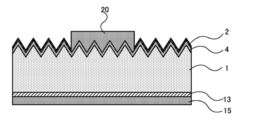
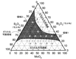
- FIG. 1 It is a cross-sectional schematic diagram of a crystalline silicon solar cell. It is explanatory drawing based on the ternary composition figure of the ternary glass which consists of molybdenum oxide, boron oxide, and bismuth oxide. It is a scanning electron microscope (SEM) photograph of the cross section of the crystalline silicon solar cell (single crystal silicon solar cell) of a prior art, Comprising: It is a photograph of the interface vicinity of a single crystal silicon substrate and a light-incidence side electrode. It is a scanning electron microscope (SEM) photograph of the cross section of the crystalline silicon solar cell (single crystal silicon solar cell) of the present invention, and is a photograph near the interface between the single crystal silicon substrate and the light incident side electrode.
- SEM scanning electron microscope
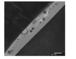
- FIG. 5 is a transmission electron microscope (TEM) photograph of the cross section of the crystalline silicon solar cell shown in FIG. 4, in which the vicinity of the interface between the single crystal silicon substrate and the light incident side electrode is enlarged.
- TEM transmission electron microscope
- FIG. 4 It is a schematic diagram for demonstrating the transmission electron micrograph of FIG.
- FIG. 4 It is a plane schematic diagram which shows the pattern for contact resistance measurement used for the measurement of the contact resistance between an electrode and a crystalline silicon substrate.
- J01 saturation current density
- Voc open circuit voltage
- crystalline silicon includes single crystal and polycrystalline silicon.
- the “crystalline silicon substrate” refers to a material obtained by forming crystalline silicon into a shape suitable for device formation, such as a flat plate shape, for the formation of electric elements or electronic elements. Any method may be used for producing crystalline silicon. For example, the Czochralski method can be used for single crystal silicon, and the casting method can be used for polycrystalline silicon. In addition, other manufacturing methods such as a polycrystalline silicon ribbon produced by a ribbon pulling method, polycrystalline silicon formed on a different substrate such as glass, and the like can also be used as the crystalline silicon substrate. Further, the “crystalline silicon solar cell” refers to a solar cell manufactured using a crystalline silicon substrate.
- FF curve factor obtained from measurement of current-voltage characteristics under light irradiation
- a contact resistance which is an electric resistance between the electrode and the impurity diffusion layer of crystalline silicon can be used.
- An impurity diffusion layer also referred to as an emitter layer is a layer in which p-type or n-type impurities are diffused, and the impurities are diffused so as to have a higher concentration than the impurity concentration in the base silicon substrate.
- one conductivity type means a p-type or n-type conductivity type
- other conductivity type means a conductivity type different from “one conductivity type”.
- one conductivity type crystalline silicon substrate is a p-type crystal silicon substrate
- another conductivity type impurity diffusion layer is an n-type impurity diffusion layer (n-type emitter layer).
- the conductive paste of the present invention is a conductive paste for forming an electrode of a crystalline silicon solar cell containing a conductive powder, a composite oxide, and an organic vehicle.
- the composite oxide of the conductive paste of the present invention contains molybdenum oxide, boron oxide and bismuth oxide.
- the conductive paste of the present invention contains a conductive powder.
- a conductive powder any single element or alloy metal powder can be used.
- a metal powder containing at least one selected from the group consisting of silver, copper, nickel, aluminum, zinc, and tin can be used.
- a single element metal powder or an alloy powder of these metals can be used.
- a conductive powder contained in the conductive paste of the present invention a conductive powder containing at least one selected from silver, copper and alloys thereof is preferably used. Among them, it is more preferable to use a conductive powder containing silver. Copper powder is preferable as an electrode material because it is relatively inexpensive and has high electrical conductivity. Moreover, silver powder has high electrical conductivity, and has been conventionally used as an electrode for many crystalline silicon solar cells, and has high reliability. Also in the case of the conductive paste of the present invention, a highly reliable and high performance crystalline silicon solar cell can be manufactured by using silver powder as the conductive powder. Therefore, it is preferable to use silver powder as the main component of the conductive powder.
- the conductive paste of the present invention can contain metal powder other than silver or alloy powder with silver as long as the performance of the solar cell electrode is not impaired.
- the conductive powder preferably contains 80% by weight or more, more preferably 90% by weight or more of the silver powder, more preferably 90% by weight or more. Is more preferably made of silver powder.
- the particle shape and particle size of the conductive powder such as silver powder are not particularly limited.
- As the particle shape for example, a spherical shape or a flake shape can be used.
- the particle size refers to the size of the longest length part of one particle.
- the particle size of the conductive powder is preferably 0.05 to 20 ⁇ m and more preferably 0.1 to 5 ⁇ m from the viewpoint of workability.
- the particle size of a large number of fine particles has a uniform distribution, it is not necessary for all the particles to have the above-mentioned particle size, and the particle size of 50% of all particles (average particle size: D50). Is preferably in the above particle size range. The same applies to the dimensions of the particles other than the conductive powder described in this specification.
- the average particle size can be determined by performing particle size distribution measurement by the microtrack method (laser diffraction scattering method) and obtaining a D50 value from the result of particle size distribution measurement.
- size of electroconductive powder such as silver powder
- the BET value of the conductive powder is preferably 0.1 to 5 m 2 / g, more preferably 0.2 to 2 m 2 / g.
- the conductive paste of the present invention contains a composite oxide containing molybdenum oxide, boron oxide and bismuth oxide.
- the composite oxide contained in the conductive paste of the present invention can be in the form of particulate composite oxide, that is, glass frit.
- FIG. 2 shows three examples of molybdenum oxide, boron oxide and bismuth oxide described in Non-Patent Document 1 (R. Iordanova, novaet al., Journal of Non-Crystalline Solids, 357 (2011) pp. 2663-2668). Explanatory drawing based on the ternary composition diagram of ternary glass is shown.
- the composition capable of vitrifying glass composed of molybdenum oxide, boron oxide, and bismuth oxide is a composition region colored in gray, which is shown as “vitrifiable region” in FIG. In the composition of the composition region shown as “non-vitrification region” in FIG. 2, vitrification cannot be performed, and thus a composite oxide having such a composition cannot exist as glass.
- the composite oxide containing molybdenum oxide, boron oxide, and bismuth oxide that can be used for the conductive paste of the present invention is a composite oxide having a composition in the “vitrifiable region” shown in FIG.
- a composite oxide containing boron oxide and bismuth oxide has a glass transition point of about 380 to 420 ° C. and a melting point of about 420 to 540 ° C., depending on the composition.
- the composite oxide contained in the conductive paste of the present invention comprises molybdenum oxide, boron oxide and bismuth oxide as a total of 100 mol%, molybdenum oxide 25 to 65 mol%, boron oxide 5 to 45 mol%, and bismuth oxide 25 to 25 mol%.
- a composition range containing 35 mol% is preferred. In FIG. 2, this composition range is shown as the composition range of the region 1.
- molybdenum oxide in the composite oxide is more in the composition range of region 1 in FIG. Preferably, it can be 35 to 65 mol%, more preferably 40 to 60 mol%.
- bismuth oxide in the composite oxide can be more preferably 28 to 32 mol% in the composition range of region 1 in FIG.
- the composite oxide contained in the conductive paste of the present invention comprises molybdenum oxide, boron oxide and bismuth oxide as a total of 100 mol%, molybdenum oxide 15 to 40 mol%, boron oxide 25 to 45 mol% and bismuth oxide 25 to 25 mol%.
- a composition range including 60 mol% is preferable. In FIG. 2, this composition range is shown as the composition range of the region 2.
- the molybdenum oxide in the composite oxide has a composition of region 2 in FIG. In the range, it can be preferably 20 to 40 mol%.
- boron oxide in the composite oxide can be preferably 20 to 40 mol% in the composition range of region 2 in FIG.
- the composite oxide contained in the conductive paste of the present invention preferably contains 90 mol% or more, preferably 95 mol% or more of the total of molybdenum oxide, boron oxide and bismuth oxide in 100 mol% of the composite oxide.
- the composite oxide contained in the conductive paste of the present invention preferably further contains 0.1 to 6 mol%, preferably 0.1 to 5 mol% of titanium oxide in 100 wt% of the composite oxide.
- the composite oxide further contains a predetermined proportion of titanium oxide, better electrical contact can be obtained.
- the composite oxide contained in the conductive paste of the present invention preferably further contains 0.1 to 3 mol%, preferably 0.1 to 2.5 mol% of zinc oxide in 100 wt% of the composite oxide. .
- the composite oxide further contains a predetermined proportion of zinc oxide, better electrical contact can be obtained.
- the conductive paste of the present invention can contain 0.1 to 10 parts by weight, more preferably 0.5 to 8 parts by weight of the composite oxide with respect to 100 parts by weight of the conductive powder. If a large amount of non-conductive complex oxide is present in the electrode, the electrical resistance of the electrode will increase. When the composite oxide of the conductive paste of the present invention is in a predetermined range, an increase in electrical resistance of the formed electrode can be suppressed.
- the composite oxide of the conductive paste of the present invention can contain any oxide other than the above oxides as long as the predetermined performance of the composite oxide is not lost.
- the composite oxide of the conductive paste of the present invention includes Al 2 O 3 , P 2 O 5 , CaO, MgO, ZrO 2 , Li 2 O 3 , Na 2 O 3 , CeO 2 , SnO 2 and SrO.
- the selected oxide can be included as appropriate.
- the shape of the composite oxide particles is not particularly limited, and for example, spherical or indefinite shapes can be used.
- the particle size is not particularly limited, but from the viewpoint of workability, the average particle size (D50) is preferably in the range of 0.1 to 10 ⁇ m, and more preferably in the range of 0.5 to 5 ⁇ m.
- the composite oxide that can be included in the conductive paste of the present invention can be produced, for example, by the following method.
- a composite oxide having an average particle size of 149 ⁇ m (median diameter, D50) can be obtained.
- the size of the composite oxide is not limited to the above example, and a composite oxide having a larger average particle size or a smaller average particle size can be obtained depending on the size of the sieve mesh. .
- a composite oxide having a predetermined average particle diameter (D50) can be obtained.
- the conductive paste of the present invention contains an organic vehicle.
- the organic vehicle contained in the conductive paste of the present invention can contain an organic binder and a solvent.
- the organic binder and the solvent play a role of adjusting the viscosity of the conductive paste and are not particularly limited. It is also possible to use an organic binder dissolved in a solvent.
- a cellulose resin for example, ethyl cellulose, nitrocellulose and the like
- a (meth) acrylic resin for example, polymethyl acrylate and polymethyl methacrylate
- the addition amount of the organic binder is usually 0.2 to 30 parts by weight, preferably 0.4 to 5 parts by weight with respect to 100 parts by weight of the conductive powder.
- Solvents include alcohols (eg terpineol, ⁇ -terpineol, ⁇ -terpineol etc.), esters (eg hydroxy group-containing esters, 2,2,4-trimethyl-1,3-pentanediol monoisobutyrate, butyl 1 type or 2 types or more can be selected and used from carbitol acetate etc.).
- the amount of the solvent added is usually 0.5 to 30 parts by weight, preferably 5 to 25 parts by weight with respect to 100 parts by weight of the conductive powder.
- additives selected from plasticizers, antifoaming agents, dispersants, leveling agents, stabilizers, adhesion promoters, and the like can be further blended as necessary.
- plasticizers those selected from phthalic acid esters, glycolic acid esters, phosphoric acid esters, sebacic acid esters, adipic acid esters, and citric acid esters can be used.
- the method for producing a conductive paste of the present invention includes a step of mixing a conductive powder, a composite oxide, and an organic vehicle.
- the conductive paste of the present invention is produced by adding, mixing, and dispersing a conductive powder, the above-described composite oxide, and optionally other additives and additive particles to an organic binder and a solvent. can do.
- Mixing can be performed with a planetary mixer, for example. Further, the dispersion can be performed by a three roll mill. Mixing and dispersion are not limited to these methods, and various known methods can be used.
- the present invention is a method for producing a crystalline silicon solar cell using the conductive paste described above.
- the above-described conductive paste of the present invention is printed on the impurity diffusion layer 4 of the crystalline silicon substrate 1 made of n-type or p-type crystalline silicon and dried. And a step of forming an electrode by firing.
- the manufacturing method of the solar cell of this invention is demonstrated in detail.
- FIG. 1 is a schematic cross-sectional view of the vicinity of a light incident side electrode 20 of a crystalline silicon solar cell having electrodes (light incident side electrode 20 and back surface electrode 15) on both the light incident side and the back surface side.
- the crystalline silicon solar cell shown in FIG. 1 includes a light incident side electrode 20 formed on the light incident side, an antireflection film 2, an impurity diffusion layer 4 (for example, an n-type impurity diffusion layer 4), and a crystalline silicon substrate 1 ( For example, a p-type crystalline silicon substrate 1) and a back electrode 15 are provided.
- the method for manufacturing a crystalline silicon solar cell according to the present invention includes a step of preparing a crystalline silicon substrate 1 of one conductivity type, and a surface of another conductivity type on one surface of the crystalline silicon substrate 1.
- the step of forming the impurity diffusion layer 4, the step of forming the antireflection film 2 on the surface of the impurity diffusion layer 4, the above-described conductive paste of the present invention is printed on the surface of the antireflection film 2, and baking Thereby forming the light incident side electrode 20.
- the method for producing a crystalline silicon solar cell of the present invention includes a step of preparing a crystalline silicon substrate 1 of one conductivity type (p-type or n-type conductivity).
- a crystalline silicon substrate 1 for example, a B (boron) -doped p-type single crystal silicon substrate can be used.
- the surface on the light incident side of the crystalline silicon substrate 1 preferably has a pyramidal texture structure.
- the method for manufacturing a crystalline silicon solar cell of the present invention includes a step of forming an impurity diffusion layer 4 of another conductivity type on one surface of the crystalline silicon substrate 1 prepared in the above step.
- the n-type impurity diffusion layer 4 can be formed as the impurity diffusion layer 4.
- the impurity diffusion layer 4 can be formed so that the sheet resistance is 60 to 140 ⁇ / ⁇ , preferably 80 to 120 ⁇ / ⁇ .
- the buffer layer 30 is formed in a later step.
- the buffer layer 30 Due to the presence of the buffer layer 30, when the conductive paste is baked, components or impurities in the conductive paste (components or impurities that adversely affect solar cell performance) diffuse into the impurity diffusion layer 4. Can be prevented. Therefore, in the crystalline silicon solar cell of the present invention, even when the impurity diffusion layer 4 is shallower (has higher sheet resistance) than the conventional impurity diffusion layer 4, without adversely affecting the solar cell characteristics, An electrode having a low contact resistance can be formed on the crystalline silicon substrate 1. Specifically, in the method for manufacturing a crystalline silicon solar cell of the present invention, the depth at which the impurity diffusion layer 4 is formed can be 150 nm to 300 nm.
- the depth of the impurity diffusion layer 4 refers to the depth from the surface of the impurity diffusion layer 4 to the pn junction.
- the depth of the pn junction can be a depth from the surface of the impurity diffusion layer 4 until the impurity concentration in the impurity diffusion layer 4 becomes 10 16 cm ⁇ 3 .
- the method for manufacturing a crystalline silicon solar cell of the present invention includes a step of forming the antireflection film 2 on the surface of the impurity diffusion layer 4 formed in the above-described step.
- a silicon nitride film SiN film
- the silicon nitride film also has a function as a surface passivation film. Therefore, when a silicon nitride film is used as the antireflection film 2, a high-performance crystalline silicon solar cell can be obtained.
- the silicon nitride film can be formed by PECVD (Plasma Enhanced Chemical Vapor Deposition) method or the like.
- the light incident side electrode 20 is obtained by printing and baking the above-described conductive paste of the present invention on the surface of the antireflection film 2 formed as described above. Forming a step. Specifically, first, an electrode pattern printed using the conductive paste of the present invention is dried at a temperature of about 100 to 150 ° C. for several minutes (for example, 0.5 to 5 minutes). At this time, in order to form the back electrode 15, it is preferable to print a predetermined conductive paste for the back electrode 15 on the entire back surface and dry it.
- the dried conductive paste is fired in the atmosphere using a firing furnace such as a tubular furnace under the same conditions as the above firing conditions.
- the firing temperature is preferably 400 to 850 ° C., more preferably 450 to 820 ° C.
- the crystalline silicon solar cell of the present invention can be manufactured by the manufacturing method as described above. According to the method for manufacturing a crystalline silicon solar cell of the present invention, particularly for the impurity diffusion layer 4 (n-type impurity diffusion layer 4) in which an n-type impurity is diffused without adversely affecting the solar cell characteristics, An electrode having a low contact resistance (light incident side electrode 20) can be obtained.
- the contact resistance of the electrode 350m ⁇ ⁇ cm 2 or less, preferably 100 m [Omega ⁇ cm or less, more preferably 25m ⁇ ⁇ cm 2
- the contact resistance of the electrode is 100 m ⁇ ⁇ cm 2 or less, it can be used as an electrode of a single crystal silicon solar cell.
- the contact resistance of the electrode is 350 m ⁇ ⁇ cm 2 or less, there is a possibility that it can be used as an electrode of a crystalline silicon solar cell.
- the crystalline silicon solar cell including the buffer layer 30 in at least a part directly below the light incident side electrode 20 as in the crystalline silicon solar cell shown in FIG. 1 has been described as an example. It is not limited to this.
- the method for producing a crystalline silicon solar cell according to the present invention is used when producing a crystalline silicon solar cell in which both positive and negative electrodes are formed on the back surface of the crystalline silicon solar cell (back electrode type crystalline silicon solar cell). Can also be applied.
- a crystalline silicon substrate 1 of one conductivity type is prepared.
- impurity diffusion layers of one conductivity type and another conductivity type are formed in at least a part of the back surface, which is one surface of the crystalline silicon substrate 1, so as to enter each other in a comb shape.
- a silicon nitride thin film is formed on the surface of the impurity diffusion layer.
- the above-described conductive paste of the present invention is printed on at least a part of the surface of the antireflection film 2 corresponding to the region where the impurity diffusion layer of one conductivity type and another conductivity type is formed, and fired.
- a back electrode type crystalline silicon solar cell can be manufactured.
- the firing of the conductive paste can be performed under the same conditions as in the method for manufacturing a crystalline silicon solar cell that includes the buffer layer 30 in at least a part directly below the light incident side electrode 20.
- the structure of a crystalline silicon solar cell manufactured by the method for manufacturing a crystalline silicon solar cell of the present invention (hereinafter also simply referred to as “the crystalline silicon solar cell of the present invention”) will be described.
- the inventors of the present invention are not between the light incident side electrode 20 and the crystalline silicon substrate 1.
- the performance of the crystalline silicon solar cell is improved by forming the buffer layer 30 having a special structure at least at a part immediately below the light incident side electrode 20.
- FIG. 4 A scanning electron micrograph of the cross section of the crystalline silicon solar cell of the present invention is shown in FIG. 4
- a scanning electron micrograph of a cross section of a crystalline silicon solar cell having a conventional structure manufactured using a conventional conductive paste for forming a solar cell electrode is shown in FIG.
- FIG. 4 in the case of the crystalline silicon solar cell of the present invention, the portion where the silver 22 in the light incident side electrode 20 is in contact with the p-type crystalline silicon substrate 1 is shown in FIG. It is clear that the number is much higher than in the case of the crystalline silicon solar cell of the comparative example shown. It can be said that the structure of the crystalline silicon solar cell of the present invention is different from that of the conventional crystalline silicon solar cell.
- the present inventors further use a transmission electron microscope (TEM) to describe in detail the structure near the interface between the crystalline silicon substrate 1 and the light incident side electrode 20 of the crystalline silicon solar cell of the present invention. Observed.
- FIG. 5 the transmission electron microscope (TEM) photograph of the cross section of the crystalline silicon solar cell of this invention is shown.
- FIG. 6 is an explanatory diagram of the TEM photograph of FIG.
- the buffer layer 30 is formed at least at a part immediately below the light incident side electrode 20.
- the structure of the crystalline silicon solar cell of the present invention will be specifically described.
- the crystalline silicon solar cell of the present invention includes a crystalline silicon substrate 1 of one conductivity type, a light incident side electrode 20 and an antireflection film 2 formed on the light incident side surface of the crystalline silicon substrate 1, a crystalline system
- This is a crystalline silicon solar cell having a back electrode 15 formed on the back surface opposite to the light incident side surface of the silicon substrate 1.
- One surface of one conductivity type crystalline silicon substrate 1 has an impurity diffusion layer 4 of another conductivity type.
- the light incident side electrode 20 of the crystalline silicon solar cell of the present invention includes silver 22 and a composite oxide 24.
- the composite oxide 24 preferably contains molybdenum oxide, boron oxide, and bismuth oxide.
- the light incident side electrode 20 of the crystalline silicon solar cell of the present invention can be obtained by firing a conductive paste containing a composite oxide containing molybdenum oxide, boron oxide and bismuth oxide.
- the composite oxide 24 includes three components of molybdenum oxide, boron oxide, and bismuth oxide, the structure of the high-performance crystalline silicon solar cell of the present invention can be reliably obtained.
- a buffer layer 30 is further included in at least part of the light incident side electrode 20 between the light incident side electrode 20 of the crystalline silicon solar cell of the present invention and the crystalline silicon substrate 1.
- the buffer layer 30 includes a silicon oxynitride film 32 and a silicon oxide film 34 in this order from the crystalline silicon substrate 1 toward the light incident side electrode 20.
- the “buffer layer 30 immediately below the light incident side electrode 20” means that the crystal of the light incident side electrode 20 is seen when the light incident side electrode 20 is viewed as the upper side and the crystalline silicon substrate 1 is viewed as the lower side as shown in FIG. It means that the buffer layer 30 exists in the direction of the silicon substrate 1 (lower side) so as to be in contact with the light incident side electrode 20.
- the crystalline silicon substrate 1 has the predetermined buffer layer 30, a high-performance crystalline silicon solar cell can be obtained.
- the buffer layer 30 is formed only directly under the light incident side electrode 20 and is not formed in a portion where the light incident side electrode 20 does not exist.
- the silicon oxynitride film 32 in the buffer layer 30 is a SiO x N y film.
- the film thicknesses of the silicon oxynitride film 32 and the silicon oxide film 34 can be 20 to 80 nm, preferably 30 to 70 nm, more preferably 40 to 60 nm, and specifically about 50 nm, respectively.
- the thickness of the buffer layer 30 including the silicon oxynitride film 32 and the silicon oxide film 34 is 40 to 160 nm, preferably 60 to 140 nm, more preferably 80 to 120 nm, still more preferably 90 to 110 nm, specifically It can be about 100 nm.
- the silicon oxynitride film 32 and the silicon oxide film 34 and the buffer layer 30 including them are in the above-described composition and thickness range, it is possible to reliably obtain a high-performance crystalline silicon solar cell.
- the buffer layer 30 uses the conductive paste containing the above-described composite oxide containing molybdenum oxide, boron oxide, and bismuth oxide to print the pattern of the light incident side electrode 20 on the crystalline silicon substrate 1 and fire it. Can be formed.
- the reason why a high-performance crystalline silicon solar cell can be obtained by including the buffer layer 30 in at least a part immediately below the light incident side electrode 20 is as follows. Note that this estimation does not limit the present invention. That is, although the silicon oxynitride film 32 and the silicon oxide film 34 are insulating films, they are considered to contribute to electrical contact between the single crystal silicon substrate 1 and the light incident side electrode 20 in some form. It is done.
- the buffer layer 30 prevents the components or impurities in the conductive paste (components or impurities that adversely affect solar cell performance) from diffusing into the impurity diffusion layer 4 when the conductive paste is baked. It is thought that it plays a role to do.
- the buffer layer 30 can prevent adverse effects on the solar cell characteristics during firing for electrode formation. Therefore, the crystalline silicon solar cell includes a silicon oxynitride film 32 and a silicon oxide film on at least part of the light incident side electrode 20 between the light incident side electrode 20 and the crystalline silicon substrate 1. It can be presumed that a high-performance crystalline silicon solar cell characteristic can be obtained by the structure having the buffer layer 30 containing 34 in this order.
- the buffer layer 30 is considered to play a role of preventing components or impurities in the conductive paste (impurities that adversely affect solar cell performance) from diffusing into the impurity diffusion layer 4. . Therefore, when the type of metal constituting the conductive powder in the conductive paste is a type of metal that adversely affects the solar cell characteristics by diffusing into the impurity diffusion layer 4, due to the presence of the buffer layer 30, An adverse effect on the solar cell characteristics can be prevented. For example, copper has a greater tendency to adversely affect solar cell characteristics by diffusing into the impurity diffusion layer 4 than silver. Therefore, when using relatively inexpensive copper as the conductive powder of the conductive paste, the effect of preventing the adverse effect on the solar cell characteristics due to the presence of the buffer layer 30 becomes particularly significant.
- the crystalline silicon solar cell of the present invention includes a finger electrode portion for the light incident side electrode 20 to be in electrical contact with the impurity diffusion layer 4, and a conductive ribbon for taking out current to the finger electrode portion and the outside.
- a buffer layer 30 is formed between at least a part of the finger electrode portion and the crystalline silicon substrate 1 directly below the finger electrode portion. It is preferred that The finger electrode portion plays a role of collecting current from the impurity diffusion layer 4. Therefore, by having a structure in which the buffer layer 30 is formed immediately below the finger electrode portion, it is possible to more reliably obtain a high-performance crystalline silicon solar cell.
- a bus-bar electrode part plays the role which flows the electric current collected by the finger electrode part with respect to a conductive ribbon.
- the bus bar electrode portion needs to have good electrical contact between the finger electrode portion and the conductive ribbon, but the buffer layer 30 immediately below the bus bar electrode portion is not necessarily required.
- the buffer layer 30 preferably contains conductive fine particles. Since the conductive fine particles have conductivity, the contact resistance between the electrode and the crystalline silicon impurity diffusion layer 4 can be further reduced by including the conductive fine particles in the buffer layer 30. Therefore, a high performance crystalline silicon solar cell can be obtained.
- the particle size of the conductive fine particles contained in the buffer layer 30 of the crystalline silicon solar cell of the present invention is preferably 20 nm or less, more preferably 15 nm or less, and even more preferably 10 nm or less. Since the conductive fine particles contained in the buffer layer 30 have a predetermined particle size, the conductive fine particles can be stably present in the buffer layer 30, and the light incident side electrode 20 and the crystalline silicon substrate 1 The contact resistance with the impurity diffusion layer 4 can be further reduced.
- the conductive fine particles are preferably present only in the silicon oxide film 34 of the buffer layer 30. It can be presumed that a higher performance crystalline silicon solar cell can be obtained when the conductive fine particles are present only in the silicon oxide film 34 of the buffer layer 30. Therefore, the conductive fine particles are preferably not present in the silicon oxynitride film 32 but only in the silicon oxide film 34.
- the conductive fine particles contained in the buffer layer 30 of the crystalline silicon solar cell of the present invention are preferably silver fine particles 36.
- silver powder is used as the conductive powder during the production of the crystalline silicon solar cell, the conductive fine particles in the buffer layer 30 become the silver fine particles 36. As a result, a highly reliable and high performance crystalline silicon solar cell can be obtained.
- the area of the buffer layer 30 of the crystalline silicon solar cell of the present invention is 5% or more, preferably 10% or more of the area immediately below the crystalline silicon substrate 1. As described above, it is possible to reliably obtain a high-performance crystalline silicon solar cell by including the buffer layer 30 in at least part of the crystalline silicon solar cell immediately below the light incident side electrode 20. When the area where the buffer layer 30 exists immediately below the light incident side electrode 20 is a predetermined ratio or more, it is possible to more reliably obtain a high-performance crystalline silicon solar cell.
- the p-type crystalline silicon substrate 1 is used as the crystalline silicon substrate 1 is mainly described. It is also possible to use an n-type crystalline silicon substrate 1. In that case, a p-type impurity diffusion layer is disposed as the impurity diffusion layer 4 instead of the n-type impurity diffusion layer. If the conductive paste of the present invention is used, an electrode having a low contact resistance can be formed in both the p-type impurity diffusion layer and the n-type impurity diffusion layer.
- the buffer layer 30 is included in at least a part directly below the light incident side electrode 20 as in the crystalline silicon solar cell shown in FIG. 1 has been described as an example. Absent. Even when a back electrode type crystalline silicon solar cell is manufactured by the manufacturing method of the present invention, the buffer layer 30 can be formed on at least a part of the back electrode 15 immediately below. As a result, a high performance back electrode type crystalline silicon solar cell can be obtained.
- the present invention can also be applied to the formation of electrodes of devices other than solar cells.
- the above-described conductive paste of the present invention is used as a conductive paste for forming electrodes such as semiconductor devices and light-emitting devices (LEDs) using a general crystalline silicon substrate 1 other than solar cells. be able to.
- a monocrystalline silicon solar cell was prototyped using the conductive paste of the present invention, and the solar cell characteristics were measured.
- a contact resistance measurement electrode was prepared using the conductive paste of the present invention, and the contact resistance between the formed electrode and the impurity diffusion layer 4 of the single crystal silicon substrate was measured, Whether or not the conductive paste of the present invention can be used was determined.
- the cross-sectional shape of the prototype single crystal silicon solar cell was observed using a scanning electron microscope (SEM) and a transmission electron microscope (TEM), whereby the structure of the crystalline silicon solar cell of the present invention was measured. Revealed.
- the electric characteristics of the single crystal silicon solar cell manufactured using the conductive paste of the present invention were evaluated by Experiments 4 to 6.
- ⁇ Material and preparation ratio of conductive paste> The composition of the conductive paste used for the trial production of the single crystal silicon solar cell of Experiment 1 and the production of the contact resistance measurement electrode of Experiment 2 is as follows.
- -Conductive powder Ag (100 weight part).
- Organic binder Ethyl cellulose (2 parts by weight) having an ethoxy content of 48 to 49.5% by weight was used.
- -Plasticizer Oleic acid (0.2 parts by weight) was used.
- Solvent Butyl carbitol (5 parts by weight) was used.
- Composite oxide (glass frit) Table 1 shows the types of composite oxides (glass frit) used in the production of the single crystal silicon solar cells of Examples 1, 2 and Comparative Examples 1 to 6 (A1, A2). , B1, B2, C1, C2, D1 and D2). Table 2 shows specific compositions of the composite oxides (glass frit) A1, A2, D1, and D2.
- the weight ratio of the composite oxide in the conductive paste was 2 parts by weight.
- a composite oxide having a glass frit shape was used.
- the average particle diameter D50 of the glass frit was 2 ⁇ m.
- the composite oxide is also referred to as glass frit.
- the method for producing the composite oxide is as follows.
- the oxide powder (glass frit component) as a raw material shown in Table 1 was weighed, mixed, and put into a crucible.
- Table 2 illustrates specific blending ratios of the composite oxides (glass frit) A1, A2, D1, and D2.
- the crucible was placed in a heated oven and the temperature of the crucible was raised to the melting temperature (Melt ⁇ temperature) and maintained until the raw material was sufficiently melted at the melting temperature. Next, the crucible was taken out from the oven, the molten contents were uniformly stirred, and the contents of the crucible were quenched at room temperature using two stainless steel rolls to obtain a plate-like glass.
- a plate-like glass was uniformly dispersed while being pulverized in a mortar, and sieved with a mesh sieve to obtain a composite oxide having a desired particle size.
- a composite oxide having an average particle diameter of 149 ⁇ m (median diameter, D50) could be obtained by passing through a 100 mesh sieve and sieving what remains on the 200 mesh sieve. Further, the composite oxide was further pulverized to obtain a composite oxide having an average particle diameter D50 of 2 ⁇ m.
- a conductive paste was prepared using the above-described materials such as conductive powder and composite oxide. Specifically, a conductive paste was prepared by mixing the materials of the above-mentioned predetermined preparation ratio with a planetary mixer, further dispersing with a three-roll mill, and forming a paste.
- the substrate used was a B (boron) -doped p-type single crystal silicon substrate (substrate thickness 200 ⁇ m).
- the substrate surface was removed by etching with a mixed solution of hydrogen fluoride, pure water and ammonium fluoride. Furthermore, heavy metal cleaning was performed with an aqueous solution containing hydrochloric acid and hydrogen peroxide.
- a texture (uneven shape) was formed on the surface of the substrate by wet etching. Specifically, a pyramidal texture structure was formed on one side (surface on the light incident side) by a wet etching method (sodium hydroxide aqueous solution). Thereafter, it was washed with an aqueous solution containing hydrochloric acid and hydrogen peroxide.
- phosphorus oxychloride (POCl 3 ) is used on the surface having the texture structure of the substrate, and phosphorus is diffused by a diffusion method at a temperature of 810 ° C. for 30 minutes, so that the n-type impurity diffusion layer 4 is about 0.28 ⁇ m.
- the n-type impurity diffusion layer 4 was formed so as to have a depth.
- the sheet resistance of the n-type impurity diffusion layer 4 was 100 ⁇ / ⁇ .
- a silicon nitride thin film (antireflection film 2) having a thickness of about 60 nm was formed on the surface of the substrate on which the n-type impurity diffusion layer 4 was formed by using a silane gas and an ammonia gas by a plasma CVD method.
- the single crystal silicon solar cell substrate thus obtained was cut into a 15 mm ⁇ 15 mm square and used.
- the conductive paste for the light incident side (surface) electrode was printed by a screen printing method.
- printing is performed with a pattern composed of a bus bar electrode portion having a width of 2 mm and six finger electrode portions having a length of 14 mm and a width of 100 ⁇ m so that the film thickness is about 20 ⁇ m. And dried at 150 ° C. for about 60 seconds.
- the conductive paste for the back electrode 15 was printed by a screen printing method.
- a conductive paste mainly composed of aluminum particles, composite oxide, ethyl cellulose, and a solvent was printed on the back surface of the above-mentioned substrate at 14 mm square and dried at 150 ° C. for about 60 seconds.
- the film thickness of the conductive paste for the back electrode 15 after drying was about 20 ⁇ m.
- a substrate on which the conductive paste is printed on the front and back surfaces is subjected to predetermined conditions in the atmosphere using a near-infrared baking furnace (DESPATCH high-speed baking furnace for solar cells) using a halogen lamp as a heating source.
- the firing conditions were a peak temperature of 800 ° C., and both sides were fired simultaneously in the atmosphere in and out of the firing furnace for 60 seconds.
- a single-crystal silicon solar cell was prototyped as described above.
- the measurement of the electrical characteristics of the solar battery cell was performed as follows. That is, the current-voltage characteristics of the prototype single crystal silicon solar cell were measured under irradiation of solar simulator light (AM1.5, energy density 100 mW / cm 2 ), and the fill factor (FF), open-circuit voltage ( Voc), short circuit current density (Jsc), and conversion efficiency ⁇ (%) were calculated. Two samples having the same conditions were prepared, and the measured value was obtained as an average value of the two samples.
- the characteristics of the single crystal silicon solar cells of Comparative Examples 1 to 6 were lower than those of the single crystal silicon solar cells of Example 1 and Example 2.
- the fill factor (FF) was particularly high. This suggests that in the single crystal silicon solar cells of Example 1 and Example 2, the contact resistance between the light incident side electrode 20 and the impurity diffusion layer 4 of the single crystal silicon substrate was low.
- the open circuit voltage (Voc) was higher than those of Comparative Examples 1 to 6. This suggests that the surface recombination rate of the carriers is lower in the single crystal silicon solar cells of Example 1 and Example 2 than in Comparative Examples 1-6.
- the recombination current J02 was lower than those of Comparative Examples 1-6. This suggests that the recombination rate of carriers in the depletion layer of the pn junction inside the single crystal silicon solar cells of Example 1 and Example 2 is low. That is, in the single crystal silicon solar cells of Example 1 and Example 2, compared with Comparative Examples 1 to 6, the recombination level density caused by diffusion of impurities contained in the conductive paste in the vicinity of the pn junction. Is suggested to be low.
- the light incident side electrode 20 is formed on the single crystal silicon solar cell having the antireflection film 2 made of a silicon nitride thin film or the like on the surface. At this time, it was found that the contact resistance between the light incident side electrode 20 and the emitter layer is low, and good electrical contact can be obtained. This means that when the conductive paste of the present invention is used, an electrode having good electrical contact can be formed when forming an electrode on the surface of a general crystalline silicon substrate 1. Is suggested.
- Example 2 Preparation of electrode for contact resistance measurement>
- an electrode was formed on the surface of the crystalline silicon substrate 1 having the impurity diffusion layer 4 using a conductive paste containing composite oxides having different compositions, and contact resistance was measured. did.
- a contact resistance measurement pattern using the conductive paste of the present invention is screen-printed on a single crystal silicon substrate having a predetermined impurity diffusion layer 4, dried, and baked to measure contact resistance.
- An electrode was obtained.
- Table 4 shows the compositions of the composite oxide (glass frit) in the conductive paste used in Experiment 2 as samples a to g.
- the compositions corresponding to the composite oxides (glass frit) of the samples a to g are shown.
- the method for producing the contact resistance measuring electrode is as follows.
- the substrate is a p-type single crystal silicon substrate (substrate thickness 200 ⁇ m) doped with B (boron), the substrate surface is removed, and heavy metal cleaning is performed. went.
- a texture (uneven shape) was formed on the surface of the substrate by wet etching. Specifically, a pyramidal texture structure was formed on one side (surface on the light incident side) by a wet etching method (sodium hydroxide aqueous solution). Thereafter, it was washed with an aqueous solution containing hydrochloric acid and hydrogen peroxide.
- phosphorus oxychloride (POCl 3 ) was used on the surface of the substrate, and phosphorus was diffused at a temperature of 810 ° C. for 30 minutes by a diffusion method.
- the n-type impurity diffusion layer 4 was formed so as to have a sheet resistance of 100 ⁇ / ⁇ .
- the contact resistance measurement substrate thus obtained was used for the production of a contact resistance measurement electrode.
- the conductive paste was printed on the contact resistance measurement substrate by a screen printing method.
- a contact resistance measurement pattern was printed on the substrate so that the film thickness was about 20 ⁇ m, and then dried at 150 ° C. for about 60 seconds.
- the contact resistance measurement pattern is a pattern in which five rectangular electrode patterns having a width of 0.5 mm and a length of 13.5 mm are arranged so that the intervals are 1, 2, 3, and 4 mm, respectively. Was used.
- the substrate printed with the contact resistance measurement pattern with the conductive paste on the surface as described above is used in the atmosphere. And calcining under predetermined conditions.
- the firing conditions were the same as in the trial production of the single crystal silicon solar cell in Experiment 1, with a peak temperature of 800 ° C., and firing was performed in the firing furnace in-out for 60 seconds in the atmosphere.
- a contact resistance measuring electrode was prototyped. Three samples having the same conditions were prepared, and the measured values were obtained as an average value of the three samples.
- the contact resistance was measured using the electrode pattern shown in FIG. 7 as described above.
- the contact resistance was determined by measuring the electrical resistance between the predetermined rectangular electrode patterns shown in FIG. 7 and separating the contact resistance component and the sheet resistance component.
- the contact resistance is 100 m ⁇ ⁇ cm 2 or less, it can be used as an electrode of a single crystal silicon solar cell.
- the contact resistance is 25 m ⁇ ⁇ cm 2 or less, it can be preferably used as an electrode of a crystalline silicon solar cell.
- the contact resistance is 10 m ⁇ ⁇ cm 2 or less, it can be more preferably used as an electrode of a crystalline silicon solar cell.
- the contact resistance is 350 m ⁇ ⁇ cm 2 or less, there is a possibility that it can be used as an electrode of a crystalline silicon solar cell.
- the contact resistance exceeds 350 m ⁇ ⁇ cm 2 , it is difficult to use as an electrode of a crystalline silicon solar cell.
- FIG. 2 shows regions including the composition range of the composite oxide (glass frit) of samples b to f as region 1 and region 2.
- the composition range of region 1 in FIG. 2 is a composition in the range of 35 to 65 mol% molybdenum oxide, 5 to 45 mol% boron oxide, and 25 to 35 mol% bismuth oxide, where the total of boron oxide and bismuth oxide is 100 mol%. It is an area.
- Example 3 Structure of crystalline silicon solar cell> A cross section of a single crystal silicon solar cell prototyped using the conductive paste containing the composite oxide (glass frit) shown in Table 4 in the same manner as in Example 1 except for the composition of the composite oxide The structure of the crystalline silicon solar cell of the present invention was clarified by observing the shape using a scanning electron microscope (SEM) and a transmission electron microscope (TEM).
- SEM scanning electron microscope
- TEM transmission electron microscope
- FIG. 4 is a scanning electron microscope (SEM) of the cross section of the crystalline silicon solar cell of the present invention, and shows a scanning electron micrograph near the interface between the single crystal silicon substrate and the light incident side electrode 20.
- FIG. 3 shows a scanning electron microscope of a cross section of a crystalline silicon solar cell prototyped by the same method as in Comparative Example 5, in the vicinity of the interface between the single crystal silicon substrate and the light incident side electrode 20.
- a scanning electron micrograph is shown.
- FIG. 5 is a transmission electron microscope (TEM) photograph of a cross section of the crystalline silicon solar cell shown in FIG. 4, showing an enlarged photograph of the vicinity of the interface between the single crystal silicon substrate and the light incident side electrode 20.
- FIG. 6 is a schematic diagram for explaining the transmission electron micrograph of FIG.
- the area of the portion where the silver 22 in the light incident side electrode 20 is in contact with the p-type crystalline silicon substrate 1 Is estimated to be 5% or more, or approximately 10% or more, of the area immediately below the light incident side electrode 20 between the light incident side electrode 20 and the single crystal silicon substrate. .
- FIG. 5 shows this TEM photograph.
- FIG. 6 is a schematic diagram for explaining the structure of the TEM photograph of FIG.
- the buffer layer 30 including the silicon oxynitride film 32 and the silicon oxide film 34 exists between the single crystal silicon substrate 1 and the light incident side electrode 20.
- the portion where the silver 22 in the incident side electrode 20 and the p-type crystalline silicon substrate 1 seem to be in contact is observed in detail using a TEM.
- the silicon oxynitride film 32 and the silicon oxide film 34 are insulating films, they contribute to electrical contact between the single crystal silicon substrate 1 and the light incident side electrode 20 in some form. It is thought that.
- the buffer layer 30 has a negative effect on the solar cell characteristics by diffusing components or impurities in the conductive paste into the p-type or n-type impurity diffusion layer 4 when firing the conductive paste. It is thought to play a role to prevent. Therefore, the structure having the buffer layer 30 including the silicon oxynitride film 32 and the silicon oxide film 34 in this order at least at a part immediately below the light incident side electrode 20 of the crystalline silicon solar cell provides high performance. It can be assumed that crystalline silicon solar cell characteristics can be obtained. Furthermore, it can be assumed that the silver fine particles 36 contained in the buffer layer 30 further contribute to the electrical contact between the single crystal silicon substrate 1 and the light incident side electrode 20.
- Example 4 Trial Manufacture of Single Crystal Silicon Solar Cell Using n-type Impurity Diffusion Layer 4 with Low Impurity Concentration>
- the n-type impurity concentration is 8 ⁇ 10 19 cm ⁇ 3 (junction depth 250 to 300 nm, sheet resistance: 130 ⁇ / ⁇ ).
- a single crystal silicon solar cell of Example 3 was made in the same manner as Example 1 except that the firing temperature (peak temperature) of the conductive paste for electrode formation was 750 ° C. That is, the composite oxide (glass frit) in the conductive paste used in Example 3 was A1 shown in Table 2.
- a single crystal silicon solar cell of Example 4 was made in the same manner as Example 3 except that the firing temperature (peak temperature) of the conductive paste was 775 ° C. Three solar cells having the same conditions were produced, and the measured values were obtained as an average value of the three.
- a single crystal silicon solar cell of Comparative Example 7 was used in the same manner as in Example 3 except that D1 shown in Table 2 was used as the composite oxide (glass frit) in the conductive paste. Prototyped.
- a single-crystal silicon solar cell of Comparative Example 8 was prototyped in the same manner as Comparative Example 7 except that the firing temperature (peak temperature) of the conductive paste was 775 ° C. Three solar cells having the same conditions were produced, and the measured values were obtained as an average value of the three.
- the impurity concentration of the emitter layer of the single crystal silicon solar cell is 2 to 3 ⁇ 10 20 cm ⁇ 3 (sheet resistance: 90 ⁇ / ⁇ ). Therefore, the impurity concentration of the emitter layer of the single crystal silicon solar cells of Example 3, Example 4, Comparative Example 7 and Comparative Example 8 is 1/3 to 1 compared with the impurity concentration of the emitter layer of a normal solar cell.
- the impurity concentration is as low as about / 4. Generally, when the impurity concentration of the emitter layer is low, the contact resistance between the electrode and the crystalline silicon substrate 1 becomes high, and it becomes difficult to obtain a crystalline silicon solar cell with good performance.
- Table 5 shows the solar cell characteristics of the single crystal silicon solar cells of Example 3, Example 4, Comparative Example 7, and Comparative Example 8. As shown in Table 5, the fill factors of Comparative Example 7 and Comparative Example 8 were low values of 0.534 and 0.717. On the other hand, the fill factor of Example 3 and Example 4 exceeded 0.76. Moreover, the conversion efficiency of the single crystal silicon solar cells of Example 3 and Example 4 was as high as 18.9% or more. Therefore, it can be said that the single crystal silicon solar cell of the present invention can obtain a high performance crystalline silicon solar cell even when the impurity concentration of the emitter layer is low.
- Example 5 Impurity concentration of n-type impurity diffusion layer 4 and saturation current density of emitter directly under electrode>
- single crystal silicon solar cells of Examples 5 to 7 were made in the same manner as Example 1 except that the impurity concentration of the emitter layer was changed. That is, A1 in Table 2 was used as the composite oxide (glass frit) in the conductive paste for Examples 5 to 7.
- single crystal silicon solar cells of Comparative Examples 9 to 11 were made in the same manner as in Examples 5 to 7 except that D1 in Table 2 was used as the composite oxide (glass frit) in the conductive paste.
- the saturation current density (J 01 ) of the emitter layer directly under the light incident side electrode 20 of the solar cell obtained as Experiment 5 was measured.
- ⁇ Experiment 6 Relationship between the area of the dummy electrode portion, the open circuit voltage, and the saturation current density of the emitter>
- a monocrystalline silicon solar cell was manufactured by changing the area of the dummy electrode portion on the emitter layer, and the open-circuit voltage, which is one of the solar cell characteristics, and the saturation current density of the emitter were measured.
- the dummy electrode part is an electrode that is not electrically connected to the bus bar electrode part (not connected to the bus bar electrode part). The surface recombination of carriers at the dummy electrode portion increases in proportion to the area of the dummy electrode portion.
- FIGS. 11, 12, and 13 are schematic diagrams of electrode shapes in which the dummy finger electrode portions 54 between the connection finger electrode portions 52 are one, two, and three. In the actual electrode shape, 64 connection finger electrode portions 52 (width 100 ⁇ m, length 140 mm) are orthogonal to each other with respect to one bus bar electrode portion 50 (width 2 mm, length 140 mm).
- the bus-bar electrode part 50 and the connection finger electrode part 52 were arrange
- the center interval between the connecting finger electrode portions 52 was 2.443 mm.
- the dummy finger electrode portion 54 was formed in a dashed line shape having a length of 5 mm and a width of 100 ⁇ m continuously arranged at an interval of 1 mm.
- the broken-line dummy finger electrode portions 54 are arranged between the connection finger electrode portions 52 at a predetermined number and at equal intervals.
- the bus bar electrode part 50 and the connecting finger electrode part 52 are connected so that current can be taken out to the outside and can measure solar cell measurement.
- the dummy finger electrode portion 54 is not connected to the bus bar electrode portion 50 and is isolated.
Landscapes
- Chemical & Material Sciences (AREA)
- Life Sciences & Earth Sciences (AREA)
- Engineering & Computer Science (AREA)
- Chemical Kinetics & Catalysis (AREA)
- General Chemical & Material Sciences (AREA)
- Geochemistry & Mineralogy (AREA)
- Materials Engineering (AREA)
- Organic Chemistry (AREA)
- Dispersion Chemistry (AREA)
- Physics & Mathematics (AREA)
- Spectroscopy & Molecular Physics (AREA)
- Inorganic Chemistry (AREA)
- Photovoltaic Devices (AREA)
- Conductive Materials (AREA)
- Sustainable Development (AREA)
- Electrodes Of Semiconductors (AREA)
- Crystallography & Structural Chemistry (AREA)
Abstract
Description
本発明の構成1は、導電性粉末と、複合酸化物と、有機ビヒクルとを含む導電性ペーストであって、複合酸化物が、酸化モリブデン、酸化ホウ素及び酸化ビスマスを含む、導電性ペーストである。本発明の構成1の導電性ペーストにより、結晶系シリコン基板の表面に対して電極を形成する際に、良好な電気的接触の電極を形成することができる。具体的には、本発明の構成1の導電性ペーストにより、窒化ケイ素薄膜等を材料とする反射防止膜を表面に有する結晶系シリコン太陽電池に対して光入射側電極を形成する際に、太陽電池特性に対して悪影響を及ぼさずに、光入射側電極と、不純物拡散層との間の接触抵抗が低く、良好な電気的接触を得ることができる導電性ペーストを得ることができる。
本発明の構成2は、複合酸化物が、酸化モリブデン、酸化ホウ素及び酸化ビスマスの合計を100モル%として、酸化モリブデン25~65モル%、酸化ホウ素5~45モル%及び酸化ビスマス25~35モル%を含む、構成1に記載の導電性ペーストである。複合酸化物を所定の組成にすることにより、太陽電池特性に対して悪影響を及ぼさずに、所定の結晶系シリコン太陽電池の光入射側電極と、不純物拡散層との間の接触抵抗が低く、良好な電気的接触を得ることを確実にできる。
本発明の構成3は、複合酸化物が、酸化モリブデン、酸化ホウ素及び酸化ビスマスの合計を100モル%として、酸化モリブデン15~40モル%、酸化ホウ素25~45モル%及び酸化ビスマス25~60モル%を含む、構成1に記載の導電性ペーストである。複合酸化物を所定の組成にすることにより、太陽電池特性に対して悪影響を及ぼさずに、所定の結晶系シリコン太陽電池の光入射側電極と、不純物拡散層との間の接触抵抗が低く、良好な電気的接触を得ることを確実にできる。
本発明の構成4は、複合酸化物が、複合酸化物100モル%中、酸化モリブデン、酸化ホウ素及び酸化ビスマスの合計を90モル%以上含む、構成1~3のいずれかに記載の導電性ペーストである。酸化モリブデン、酸化ホウ素及び酸化ビスマスの3成分を所定割合以上にすることにより、太陽電池特性に対して悪影響を及ぼさずに、所定の結晶系シリコン太陽電池の光入射側電極と、不純物拡散層との間の接触抵抗が低く、良好な電気的接触を得ることを、より確実にできる。
本発明の構成5は、複合酸化物が、複合酸化物100重量%中、酸化チタン0.1~6モル%をさらに含む、構成1~4のいずれかに記載の導電性ペーストである。複合酸化物が所定の割合の酸化チタンをさらに含むことにより、より良好な電気的接触を得ることができる。
本発明の構成6は、複合酸化物が、複合酸化物100重量%中、酸化亜鉛0.1~3モル%をさらに含む、構成1~5のいずれかに記載の導電性ペーストである。複合酸化物が所定の割合の酸化亜鉛をさらに含むことにより、さらに良好な電気的接触を得ることができる。
本発明の構成7は、導電性ペーストが、導電性粉末100重量部に対し、複合酸化物を0.1~10重量部含む、構成1~6のいずれかに記載の導電性ペーストである。導電性ペーストの複合酸化物の含有量が、導電性粉末の含有量に対して所定の範囲であることにより、非導電性の複合酸化物が存在することによって、形成される電極の電気抵抗の上昇を抑制することができる。
本発明の構成8は、導電性粉末が、銀粉末である、構成1~7のいずれかに記載の導電性ペーストである。銀粉末は導電率が高く、従来から多くの結晶系シリコン太陽電池用の電極として用いられており、信頼性が高い。本発明の導電性ペーストの場合も、導電性粉末として銀粉末を用いることにより、信頼性が高く、高性能の結晶系シリコン太陽電池を製造することができる。
本発明の構成9は、一の導電型の結晶系シリコン基板を用意する工程と、結晶系シリコン基板の一方の表面に、他の導電型の不純物拡散層を形成する工程と、不純物拡散層の表面に、反射防止膜を形成する工程と、構成1~8のいずれかに記載の導電性ペーストを、反射防止膜の表面に印刷し、及び焼成することによって光入射側電極を形成するための、電極形成工程とを含む、結晶系シリコン太陽電池の製造方法である。光入射側電極が、上述の本発明の導電性ペーストを焼成することにより形成されることにより、所定の構造の本発明の高性能の結晶系シリコン太陽電池を製造することができる。
本発明の構成10は、一の導電型の結晶系シリコン基板を用意する工程と、結晶系シリコン基板の一方の表面である裏面の少なくとも一部に、一の導電型及び他の導電型の不純物拡散層を、それぞれ櫛状に、互いに入り込むように形成する工程と、不純物拡散層の表面に、窒化ケイ素薄膜を形成する工程と、構成1~8のいずれかに記載の導電性ペーストを、一の導電型及び他の導電型の不純物拡散層が形成された領域に対応する反射防止膜の表面の少なくとも一部に印刷し、及び焼成することによって、一の導電型及び他の導電型の不純物拡散層に、それぞれ電気的に接続する二つの電極を形成するための、電極形成工程とを含む、結晶系シリコン太陽電池の製造方法である。結晶系シリコン基板の一方の表面である裏面の電極が、上述の本発明の導電性ペーストを焼成することにより形成されることにより、所定の構造の本発明の高性能の、裏面電極型の結晶系シリコン太陽電池を製造することができる。
本発明の構成11は、電極形成工程が、導電性ペーストを、400~850℃で焼成することを含む、構成9に記載の結晶系シリコン太陽電池の製造方法である。導電性ペーストを所定の温度範囲で焼成することにより、所定の構造の本発明の高性能の結晶系シリコン太陽電池を確実に製造することができる。
実験1の単結晶シリコン太陽電池の試作、及び実験2の接触抵抗測定用電極の作製に用いた導電性ペーストの組成は、下記の通りである。
・導電性粉末: Ag(100重量部)。球状、BET値が1.0m2/g、平均粒径D50が1.4μmのものを用いた。
・有機バインダ: エチルセルロース(2重量部)、エトキシ含有量48~49.5重量%のものを用いた。
・可塑剤: オレイン酸(0.2重量部)を用いた。
・溶剤: ブチルカルビトール(5重量部)を用いた。
・複合酸化物(ガラスフリット): 表1に、実施例1、実施例2及び比較例1~6の単結晶シリコン太陽電池の製造に用いた複合酸化物(ガラスフリット)の種類(A1、A2、B1、B2、C1、C2、D1及びD2)を示す。表2に、複合酸化物(ガラスフリット)A1、A2、D1及びD2の具体的な組成を示す。なお、導電性ペースト中の複合酸化物の重量割合は、2重量部とした。また、複合酸化物として、ガラスフリットの形状のものを用いた。ガラスフリットの平均粒径D50は2μmとした。本実施例では、複合酸化物をガラスフリットともいう。
実験1として、調製した導電性ペーストを用いて単結晶シリコン太陽電池を試作し、その特性を測定することによって、本発明の導電性ペーストの評価を行った。単結晶シリコン太陽電池の試作方法は次の通りである。
太陽電池セルの電気的特性の測定は、次のように行った。すなわち、試作した単結晶シリコン太陽電池の電流-電圧特性を、ソーラーシミュレータ光(AM1.5、エネルギー密度100mW/cm2)の照射下で測定し、測定結果から曲線因子(FF)、開放電圧(Voc)、短絡電流密度(Jsc)及び変換効率η(%)を算出した。なお、試料は同じ条件のものを2個作製し、測定値は2個の平均値として求めた。
表1及び表2に示す複合酸化物(ガラスフリット)を用いた実施例1及び2、並びに比較例1~6の導電性ペーストを製造した。それらの導電性ペーストを単結晶シリコン太陽電池の光入射側電極20の形成のために用いて、上述のような方法で、実験1の単結晶シリコン太陽電池を試作した。表3に、これらの単結晶シリコン太陽電池の特性である曲線因子(FF)、開放電圧(Voc)、短絡電流密度(Jsc)及び変換効率η(%)の測定結果を示す。なお、これらの単結晶シリコン太陽電池に対してさらに、Suns-Vocの測定を行い、再結合電流(J02)を測定した。Suns-Vocの測定の測定方法及び測定結果から再結合電流J02を算出する方法は公知である。
実験2では、本発明の導電性ペーストにおいて、組成の異なる複合酸化物を含む導電性ペーストを用いて、不純物拡散層4を有する結晶系シリコン基板1の表面に電極を形成し、接触抵抗を測定した。具体的には、本発明の導電性ペーストを用いた接触抵抗測定用パターンを、所定の不純物拡散層4を有する単結晶シリコン基板にスクリーン印刷し、乾燥し、焼成することにより、接触抵抗測定用電極を得た。表4に、実験2で用いた導電性ペースト中の複合酸化物(ガラスフリット)の組成を、試料a~gとして示す。また、図2の3種類の酸化物の三元組成図上に、試料a~gの複合酸化物(ガラスフリット)に対応する組成を示す。接触抵抗測定用電極の作製方法は次の通りである。
表4に示す試料dの複合酸化物(ガラスフリット)を含む導電性ペーストを用いて、複合酸化物の組成以外は、上述の実施例1と同様の方法で試作した単結晶シリコン太陽電池の断面形状を走査型電子顕微鏡(SEM)及び透過型電子顕微鏡(TEM)を用いて観察することによって、本発明の結晶系シリコン太陽電池の構造を明らかにした。
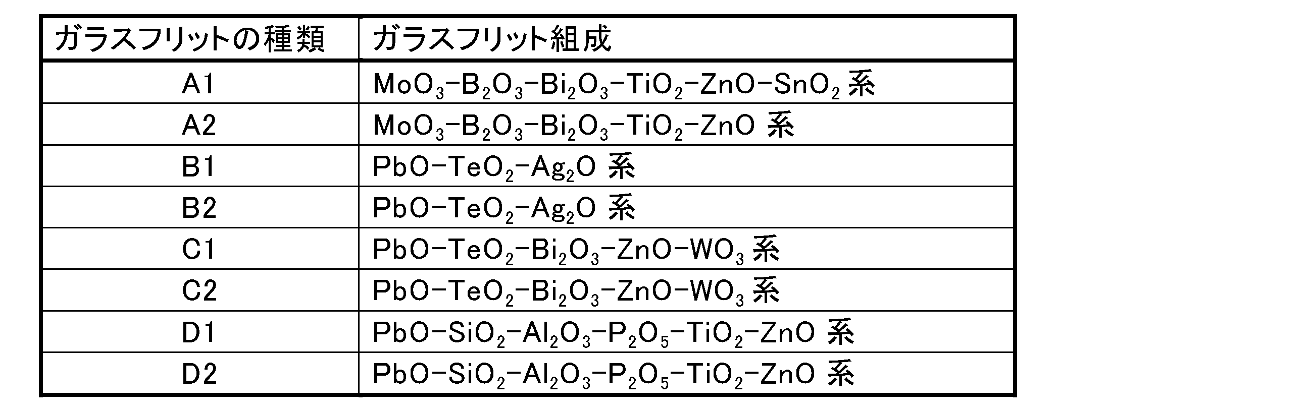
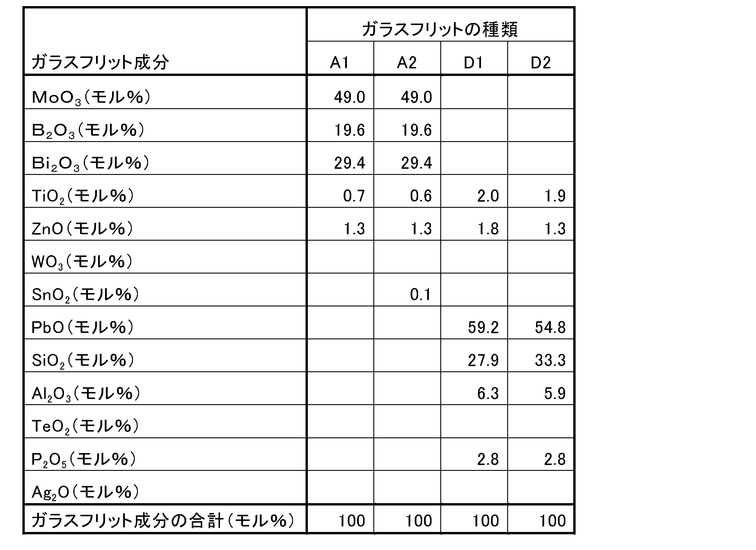

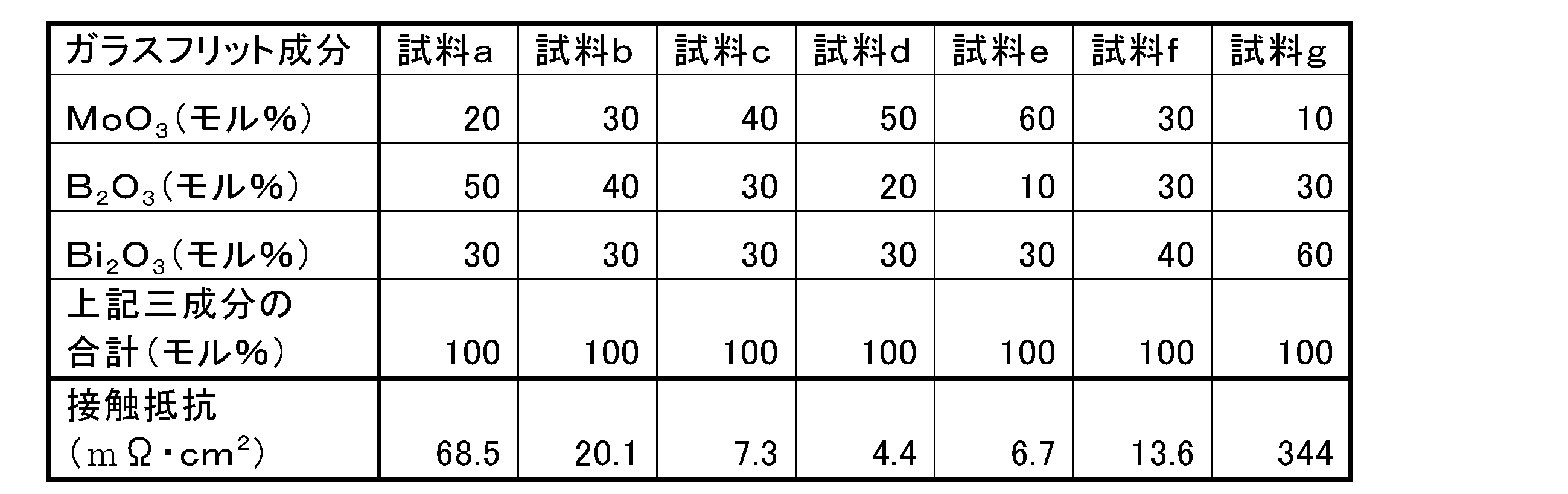
実験4の実施例として、n型不純物拡散層4(エミッタ層)を形成する際に、n型不純物濃度を8×1019cm-3(接合深さ250~300nm、シート抵抗:130Ω/□)とし、電極形成のための導電性ペーストの焼成温度(ピーク温度)を750℃とした以外は、実施例1と同様にして、実施例3の単結晶シリコン太陽電池を試作した。すなわち、実施例3で用いた導電性ペースト中の複合酸化物(ガラスフリット)は、表2に記載のA1だった。また、導電性ペーストの焼成温度(ピーク温度)を775℃とした以外は、実施例3と同様にして、実施例4の単結晶シリコン太陽電池を試作した。なお、太陽電池は同じ条件のものを3個作製し、測定値は3個の平均値として求めた。
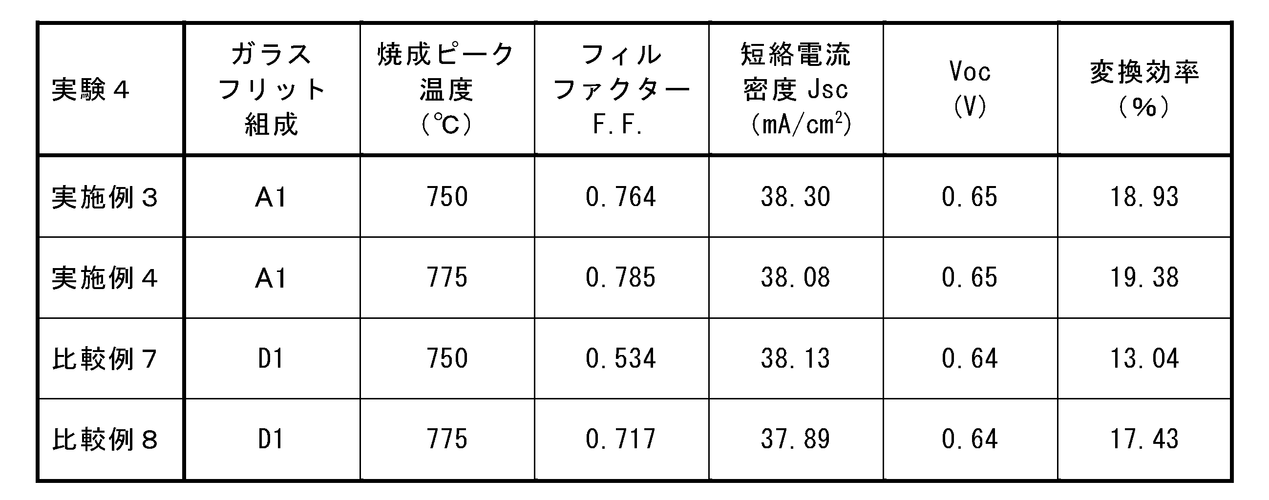
実験5として、エミッタ層の不純物濃度を変化させた以外は実施例1と同様に、実施例5~7の単結晶シリコン太陽電池を試作した。すなわち、実施例5~7のための導電性ペースト中の複合酸化物(ガラスフリット)は、表2のA1を用いた。また、導電性ペースト中の複合酸化物(ガラスフリット)として表2のD1を用いた以外は実施例5~7と同様に、比較例9~11の単結晶シリコン太陽電池を試作した。実験5として得られた太陽電池の、光入射側電極20の直下のエミッタ層の飽和電流密度(J01)を測定した。なお、太陽電池は同じ条件のものを3個作製し、測定値は3個の平均値として求めた。その測定結果を図8に示す。なお、光入射側電極20の直下のエミッタ層の飽和電流密度(J01)が低いということは、光入射側電極20の直下でのキャリアの表面再結合速度が小さいことを示している。表面再結合速度が小さい場合には、光入射により発生したキャリアの再結合が小さくなるため、高い性能の太陽電池を得ることができる。

実験6として、エミッタ層上のダミー電極部の面積を変化させて、単結晶シリコン太陽電池を試作し、太陽電池特性の一つである開放電圧、及びエミッタの飽和電流密度を測定した。なお、ダミー電極部とは、バスバー電極部に電気的に接続していない(バスバー電極部に接続していない)電極である。ダミー電極部の面積に比例して、ダミー電極部でのキャリアの表面再結合が増加することになる。したがって、ダミー電極部の面積の増加と、開放電圧及びエミッタの飽和電流密度との関係を知ることにより、光入射側電極20の直下のエミッタ層表面での、キャリアの表面再結合に起因する太陽電池性能の低下の様子を明らかにすることができる。

1 結晶系シリコン基板(p型結晶系シリコン基板)
2 反射防止膜
4 不純物拡散層(n型不純物拡散層)
15 裏面電極
20 光入射側電極(表面電極)
22 銀
24 複合酸化物
30 緩衝層
32 酸窒化ケイ素膜
34 酸化ケイ素膜
36 銀微粒子
50 バスバー電極部
52 接続フィンガー電極部
54 ダミーフィンガー電極部
Claims (11)
- 導電性粉末と、複合酸化物と、有機ビヒクルとを含む導電性ペーストであって、
複合酸化物が、酸化モリブデン、酸化ホウ素及び酸化ビスマスを含む、導電性ペースト。 - 複合酸化物が、酸化モリブデン、酸化ホウ素及び酸化ビスマスの合計を100モル%として、酸化モリブデン25~65モル%、酸化ホウ素5~45モル%及び酸化ビスマス25~35モル%を含む、請求項1に記載の導電性ペースト。
- 複合酸化物が、酸化モリブデン、酸化ホウ素及び酸化ビスマスの合計を100モル%として、酸化モリブデン15~40モル%、酸化ホウ素25~45モル%及び酸化ビスマス25~60モル%を含む、請求項1に記載の導電性ペースト。
- 複合酸化物が、複合酸化物100モル%中、酸化モリブデン、酸化ホウ素及び酸化ビスマスの合計を90モル%以上含む、請求項1~3のいずれか1項に記載の導電性ペースト。
- 複合酸化物が、複合酸化物100重量%中、酸化チタン0.1~6モル%をさらに含む、請求項1~4のいずれか1項に記載の導電性ペースト。
- 複合酸化物が、複合酸化物100重量%中、酸化亜鉛0.1~3モル%をさらに含む、請求項1~5のいずれか1項に記載の導電性ペースト。
- 導電性ペーストが、導電性粉末100重量部に対し、複合酸化物を0.1~10重量部含む、請求項1~6のいずれか1項に記載の導電性ペースト。
- 導電性粉末が、銀粉末である、請求項1~7のいずれか1項に記載の導電性ペースト。
- 一の導電型の結晶系シリコン基板を用意する工程と、
結晶系シリコン基板の一方の表面に、他の導電型の不純物拡散層を形成する工程と、
不純物拡散層の表面に、反射防止膜を形成する工程と、
請求項1~8のいずれか1項に記載の導電性ペーストを、反射防止膜の表面に印刷し、及び焼成することによって光入射側電極を形成するための、電極形成工程とを含む、結晶系シリコン太陽電池の製造方法。 - 一の導電型の結晶系シリコン基板を用意する工程と、
結晶系シリコン基板の一方の表面である裏面の少なくとも一部に、一の導電型及び他の導電型の不純物拡散層を、それぞれ櫛状に、互いに入り込むように形成する工程と、
不純物拡散層の表面に、窒化ケイ素薄膜を形成する工程と、
請求項1~8のいずれか1項に記載の導電性ペーストを、一の導電型及び他の導電型の不純物拡散層が形成された領域に対応する反射防止膜の表面の少なくとも一部に印刷し、及び焼成することによって、一の導電型及び他の導電型の不純物拡散層に、それぞれ電気的に接続する二つの電極を形成するための、電極形成工程と
を含む、結晶系シリコン太陽電池の製造方法。 - 電極形成工程が、導電性ペーストを、400~850℃で焼成することを含む、請求項9又は10に記載の結晶系シリコン太陽電池の製造方法。
Priority Applications (3)
| Application Number | Priority Date | Filing Date | Title |
|---|---|---|---|
| JP2015528331A JP6487842B2 (ja) | 2013-07-25 | 2014-07-24 | 導電性ペースト及び結晶系シリコン太陽電池の製造方法 |
| KR1020167004026A KR102175305B1 (ko) | 2013-07-25 | 2014-07-24 | 도전성 페이스트 및 결정계 실리콘 태양 전지의 제조 방법 |
| CN201480041741.2A CN105409009A (zh) | 2013-07-25 | 2014-07-24 | 导电性糊剂以及结晶系硅太阳能电池的制造方法 |
Applications Claiming Priority (2)
| Application Number | Priority Date | Filing Date | Title |
|---|---|---|---|
| JP2013-154582 | 2013-07-25 | ||
| JP2013154582 | 2013-07-25 |
Publications (1)
| Publication Number | Publication Date |
|---|---|
| WO2015012352A1 true WO2015012352A1 (ja) | 2015-01-29 |
Family
ID=52393386
Family Applications (2)
| Application Number | Title | Priority Date | Filing Date |
|---|---|---|---|
| PCT/JP2014/069566 Ceased WO2015012353A1 (ja) | 2013-07-25 | 2014-07-24 | 結晶系シリコン太陽電池及びその製造方法 |
| PCT/JP2014/069565 Ceased WO2015012352A1 (ja) | 2013-07-25 | 2014-07-24 | 導電性ペースト及び結晶系シリコン太陽電池の製造方法 |
Family Applications Before (1)
| Application Number | Title | Priority Date | Filing Date |
|---|---|---|---|
| PCT/JP2014/069566 Ceased WO2015012353A1 (ja) | 2013-07-25 | 2014-07-24 | 結晶系シリコン太陽電池及びその製造方法 |
Country Status (6)
| Country | Link |
|---|---|
| US (1) | US20160155868A1 (ja) |
| JP (2) | JP6487842B2 (ja) |
| KR (1) | KR102175305B1 (ja) |
| CN (2) | CN105409009A (ja) |
| TW (2) | TWI628804B (ja) |
| WO (2) | WO2015012353A1 (ja) |
Cited By (1)
| Publication number | Priority date | Publication date | Assignee | Title |
|---|---|---|---|---|
| JP2019106524A (ja) * | 2017-12-08 | 2019-06-27 | 三星エスディアイ株式会社Samsung SDI Co., Ltd. | 太陽電池 |
Families Citing this family (11)
| Publication number | Priority date | Publication date | Assignee | Title |
|---|---|---|---|---|
| US8969122B2 (en) * | 2011-06-14 | 2015-03-03 | International Business Machines Corporation | Processes for uniform metal semiconductor alloy formation for front side contact metallization and photovoltaic device formed therefrom |
| EP3275000A1 (en) * | 2015-03-27 | 2018-01-31 | Heraeus Deutschland GmbH & Co. KG | Electro-conductive pastes comprising an oxide additive |
| KR20170014734A (ko) | 2015-07-31 | 2017-02-08 | 엘지전자 주식회사 | 태양 전지 및 이의 제조 방법 |
| EP3282453B1 (en) * | 2016-08-11 | 2023-07-12 | Henkel AG & Co. KGaA | Improved processing of polymer based inks and pastes |
| JP6714275B2 (ja) * | 2016-08-23 | 2020-06-24 | ナミックス株式会社 | 導電性ペースト及び太陽電池 |
| JP6677678B2 (ja) * | 2017-06-23 | 2020-04-08 | 信越化学工業株式会社 | 高効率太陽電池の製造方法 |
| JP7027719B2 (ja) * | 2017-08-07 | 2022-03-02 | Agc株式会社 | ガラス組成物およびガラス粉末 |
| JP6958257B2 (ja) * | 2017-11-08 | 2021-11-02 | Agc株式会社 | ガラス組成物、ガラス粉末、導電ペーストおよび太陽電池 |
| JP7161738B2 (ja) * | 2018-02-08 | 2022-10-27 | ナミックス株式会社 | 導電性ペースト、硬化物、導電性パターン、衣服及びストレッチャブルペースト |
| CN115116648B (zh) * | 2022-07-04 | 2024-09-27 | 上海玖银电子科技有限公司 | 一种用于薄膜开关的导电银浆及其制备方法 |
| EP4618162A4 (en) * | 2022-11-07 | 2026-04-15 | Namics Corp | SOLAR CELL |
Citations (7)
| Publication number | Priority date | Publication date | Assignee | Title |
|---|---|---|---|---|
| JPH04214045A (ja) * | 1990-12-11 | 1992-08-05 | Hoya Corp | 低融点ガラス |
| JPH05217421A (ja) * | 1992-02-07 | 1993-08-27 | Nippon Steel Corp | メタライズ用組成物 |
| JP2001172046A (ja) * | 1999-12-20 | 2001-06-26 | Asahi Glass Co Ltd | 隔壁形成用低融点ガラス |
| JP2003152207A (ja) * | 2001-11-13 | 2003-05-23 | Toyota Motor Corp | 光電変換素子及びその製造方法 |
| JP2012079550A (ja) * | 2010-10-01 | 2012-04-19 | Nippon Electric Glass Co Ltd | 電気素子パッケージ |
| JP2012523365A (ja) * | 2009-04-09 | 2012-10-04 | イー・アイ・デュポン・ドウ・ヌムール・アンド・カンパニー | 光起電力セル用の導体中に使用されるガラス組成物 |
| JP2014060260A (ja) * | 2012-09-18 | 2014-04-03 | Murata Mfg Co Ltd | 導電性ペースト及び太陽電池 |
Family Cites Families (25)
| Publication number | Priority date | Publication date | Assignee | Title |
|---|---|---|---|---|
| JP2006151793A (ja) * | 2004-10-29 | 2006-06-15 | Okamoto Glass Co Ltd | 電子伝導性ガラス及びこれを用いた電子線励起型ディスプレイ用スペーサ |
| US8637340B2 (en) * | 2004-11-30 | 2014-01-28 | Solexel, Inc. | Patterning of silicon oxide layers using pulsed laser ablation |
| KR100877817B1 (ko) * | 2005-11-08 | 2009-01-12 | 엘지전자 주식회사 | 고효율 태양전지 및 그것의 제조방법 |
| NL2000033C1 (nl) * | 2006-03-20 | 2007-09-21 | Univ Eindhoven Tech | Inrichting voor het omzetten van elektromagnetische stralingsenergie in elektrische energie en werkwijze ter vervaardiging van een dergelijke inrichting. |
| JP5528653B2 (ja) * | 2006-08-09 | 2014-06-25 | 信越半導体株式会社 | 半導体基板並びに電極の形成方法及び太陽電池の製造方法 |
| CN102593243A (zh) * | 2007-08-31 | 2012-07-18 | 费罗公司 | 用于太阳能电池的分层触点结构 |
| CN201112399Y (zh) * | 2007-09-27 | 2008-09-10 | 江苏林洋新能源有限公司 | 具有浓硼浓磷扩散结构的太阳能电池 |
| WO2009052266A1 (en) | 2007-10-18 | 2009-04-23 | E. I. Du Pont De Nemours And Company | Conductive compositions and processes for use in the manufacture of semiconductor devices: mg-containing additive |
| JP5215458B2 (ja) * | 2009-03-27 | 2013-06-19 | 株式会社日立製作所 | 導電性ペースト及びそれを用いた電極配線を具備する電子部品 |
| CA2759708C (en) * | 2009-04-21 | 2019-06-18 | Tetrasun, Inc. | High-efficiency solar cell structures and methods of manufacture |
| CN101555388B (zh) * | 2009-05-19 | 2012-09-05 | 无锡市儒兴科技开发有限公司 | 硅太阳能电池铝浆用无机粘合剂及其制备方法 |
| JP5559509B2 (ja) * | 2009-10-28 | 2014-07-23 | 昭栄化学工業株式会社 | 太陽電池電極形成用導電性ペースト |
| JP5559510B2 (ja) * | 2009-10-28 | 2014-07-23 | 昭栄化学工業株式会社 | 太陽電池素子及びその製造方法 |
| US8252204B2 (en) * | 2009-12-18 | 2012-08-28 | E I Du Pont De Nemours And Company | Glass compositions used in conductors for photovoltaic cells |
| US8697476B2 (en) * | 2010-04-30 | 2014-04-15 | E I Du Pont De Nemours And Company | Processes and compositions for forming photovoltaic devices with base metal buss bars |
| US9249319B2 (en) * | 2010-06-29 | 2016-02-02 | Korea University Research And Business Foundation | Liquid additive for etching silicon nitride and silicon oxide layers, metal ink containing the same, and method of manufacturing silicon solar cell electrodes |
| KR101741683B1 (ko) * | 2010-08-05 | 2017-05-31 | 삼성전자주식회사 | 도전성 페이스트, 상기 도전성 페이스트를 사용하여 형성된 전극을 포함하는 전자 소자 및 태양 전지 |
| KR101960465B1 (ko) * | 2010-10-27 | 2019-03-21 | 삼성전자주식회사 | 도전성 페이스트 및 태양 전지 |
| TWI433341B (zh) * | 2010-12-29 | 2014-04-01 | Au Optronics Corp | 太陽電池的製造方法 |
| EP2579320A2 (en) * | 2011-10-06 | 2013-04-10 | Samsung SDI Co., Ltd. | Photovoltaic device |
| TWI552975B (zh) * | 2011-10-25 | 2016-10-11 | 賀利氏貴金屬北美康舍霍肯有限責任公司 | 含有金屬奈米顆粒之導電膠組合物 |
| TWI432551B (zh) * | 2011-11-11 | 2014-04-01 | Eternal Chemical Co Ltd | 太陽能電池用之導電膠組成物及其應用 |
| WO2013148047A1 (en) * | 2012-03-30 | 2013-10-03 | Applied Materials, Inc. | Doped ai paste for local alloyed junction formation with low contact resistance |
| US8652873B1 (en) * | 2012-08-03 | 2014-02-18 | E I Du Pont De Nemours And Company | Thick-film paste containing lead-vanadium-based oxide and its use in the manufacture of semiconductor devices |
| US8912071B2 (en) * | 2012-12-06 | 2014-12-16 | International Business Machines Corporation | Selective emitter photovoltaic device |
-
2014
- 2014-07-24 CN CN201480041741.2A patent/CN105409009A/zh active Pending
- 2014-07-24 KR KR1020167004026A patent/KR102175305B1/ko active Active
- 2014-07-24 WO PCT/JP2014/069566 patent/WO2015012353A1/ja not_active Ceased
- 2014-07-24 US US14/906,438 patent/US20160155868A1/en not_active Abandoned
- 2014-07-24 JP JP2015528331A patent/JP6487842B2/ja active Active
- 2014-07-24 CN CN201480041740.8A patent/CN105408267B/zh active Active
- 2014-07-24 JP JP2015528332A patent/JP6375298B2/ja active Active
- 2014-07-24 WO PCT/JP2014/069565 patent/WO2015012352A1/ja not_active Ceased
- 2014-07-25 TW TW103125450A patent/TWI628804B/zh active
- 2014-07-25 TW TW103125452A patent/TWI628805B/zh active
Patent Citations (7)
| Publication number | Priority date | Publication date | Assignee | Title |
|---|---|---|---|---|
| JPH04214045A (ja) * | 1990-12-11 | 1992-08-05 | Hoya Corp | 低融点ガラス |
| JPH05217421A (ja) * | 1992-02-07 | 1993-08-27 | Nippon Steel Corp | メタライズ用組成物 |
| JP2001172046A (ja) * | 1999-12-20 | 2001-06-26 | Asahi Glass Co Ltd | 隔壁形成用低融点ガラス |
| JP2003152207A (ja) * | 2001-11-13 | 2003-05-23 | Toyota Motor Corp | 光電変換素子及びその製造方法 |
| JP2012523365A (ja) * | 2009-04-09 | 2012-10-04 | イー・アイ・デュポン・ドウ・ヌムール・アンド・カンパニー | 光起電力セル用の導体中に使用されるガラス組成物 |
| JP2012079550A (ja) * | 2010-10-01 | 2012-04-19 | Nippon Electric Glass Co Ltd | 電気素子パッケージ |
| JP2014060260A (ja) * | 2012-09-18 | 2014-04-03 | Murata Mfg Co Ltd | 導電性ペースト及び太陽電池 |
Cited By (1)
| Publication number | Priority date | Publication date | Assignee | Title |
|---|---|---|---|---|
| JP2019106524A (ja) * | 2017-12-08 | 2019-06-27 | 三星エスディアイ株式会社Samsung SDI Co., Ltd. | 太陽電池 |
Also Published As
| Publication number | Publication date |
|---|---|
| TW201523896A (zh) | 2015-06-16 |
| CN105408267B (zh) | 2020-01-14 |
| US20160155868A1 (en) | 2016-06-02 |
| TWI628805B (zh) | 2018-07-01 |
| KR20160034957A (ko) | 2016-03-30 |
| JPWO2015012352A1 (ja) | 2017-03-02 |
| JPWO2015012353A1 (ja) | 2017-03-02 |
| CN105409009A (zh) | 2016-03-16 |
| CN105408267A (zh) | 2016-03-16 |
| TW201519452A (zh) | 2015-05-16 |
| WO2015012353A1 (ja) | 2015-01-29 |
| TWI628804B (zh) | 2018-07-01 |
| JP6487842B2 (ja) | 2019-03-20 |
| JP6375298B2 (ja) | 2018-08-15 |
| KR102175305B1 (ko) | 2020-11-06 |
Similar Documents
| Publication | Publication Date | Title |
|---|---|---|
| JP6487842B2 (ja) | 導電性ペースト及び結晶系シリコン太陽電池の製造方法 | |
| JP6220862B2 (ja) | 電極形成用導電性ペースト、太陽電池の製造方法及び太陽電池 | |
| JP2006302890A (ja) | 半導体デバイスの製造方法、およびそこで使用される導電性組成物 | |
| JP5693265B2 (ja) | 太陽電池及びその電極形成用導電性ペースト | |
| JP6137852B2 (ja) | 太陽電池の電極形成用導電性ペースト | |
| TW201737502A (zh) | 導電性膏及太陽能電池 | |
| JP6580383B2 (ja) | 導電性ペースト、太陽電池及び太陽電池の製造方法 | |
| JP2009194121A (ja) | 結晶系シリコン太陽電池電極形成用導電性ペースト | |
| JPWO2008078375A1 (ja) | 結晶系シリコン基板の電極形成用導電性ペースト | |
| JP2011187882A (ja) | 太陽電池及びその製造方法 | |
| US10475938B2 (en) | Process for producing conductive pastes for forming solar cell electrodes | |
| US20190194059A1 (en) | Conductive paste and solar cell | |
| JP2010251645A (ja) | 太陽電池及びその電極形成用導電性ペースト | |
| JP2009194141A (ja) | 太陽電池電極形成用導電性ペースト | |
| JP5550881B2 (ja) | 太陽電池及びその製造方法 | |
| JP4714634B2 (ja) | 太陽電池電極用導電性ペースト | |
| JP2008010527A (ja) | 太陽電池電極用導電性ペースト | |
| JP6266079B2 (ja) | 太陽電池の電極形成用導電性ペースト及び太陽電池の製造方法 | |
| JP6200128B2 (ja) | 太陽電池の電極形成用導電性ペースト | |
| JP6176783B2 (ja) | 結晶系シリコン太陽電池及びその製造方法 |
Legal Events
| Date | Code | Title | Description |
|---|---|---|---|
| WWE | Wipo information: entry into national phase |
Ref document number: 201480041741.2 Country of ref document: CN |
|
| 121 | Ep: the epo has been informed by wipo that ep was designated in this application |
Ref document number: 14830327 Country of ref document: EP Kind code of ref document: A1 |
|
| ENP | Entry into the national phase |
Ref document number: 2015528331 Country of ref document: JP Kind code of ref document: A |
|
| NENP | Non-entry into the national phase |
Ref country code: DE |
|
| ENP | Entry into the national phase |
Ref document number: 20167004026 Country of ref document: KR Kind code of ref document: A |
|
| 122 | Ep: pct application non-entry in european phase |
Ref document number: 14830327 Country of ref document: EP Kind code of ref document: A1 |