WO2015001936A1 - 塗布膜の形成方法及びコンピュータ記憶媒体 - Google Patents
塗布膜の形成方法及びコンピュータ記憶媒体 Download PDFInfo
- Publication number
- WO2015001936A1 WO2015001936A1 PCT/JP2014/065576 JP2014065576W WO2015001936A1 WO 2015001936 A1 WO2015001936 A1 WO 2015001936A1 JP 2014065576 W JP2014065576 W JP 2014065576W WO 2015001936 A1 WO2015001936 A1 WO 2015001936A1
- Authority
- WO
- WIPO (PCT)
- Prior art keywords
- temperature
- substrate
- coating film
- heating step
- heating
- Prior art date
Links
- 238000000576 coating method Methods 0.000 title claims abstract description 81
- 239000011248 coating agent Substances 0.000 title claims abstract description 80
- 238000000034 method Methods 0.000 title claims abstract description 31
- 238000003860 storage Methods 0.000 title claims description 6
- 238000010438 heat treatment Methods 0.000 claims abstract description 86
- 239000000758 substrate Substances 0.000 claims abstract description 53
- 239000007788 liquid Substances 0.000 claims abstract description 29
- 238000004132 cross linking Methods 0.000 claims abstract description 18
- 239000002904 solvent Substances 0.000 claims abstract description 18
- 230000009477 glass transition Effects 0.000 claims abstract description 12
- 239000000463 material Substances 0.000 claims abstract description 6
- 238000000354 decomposition reaction Methods 0.000 claims abstract description 5
- 238000012545 processing Methods 0.000 claims description 69
- QVGXLLKOCUKJST-UHFFFAOYSA-N atomic oxygen Chemical compound [O] QVGXLLKOCUKJST-UHFFFAOYSA-N 0.000 claims description 20
- 229910052760 oxygen Inorganic materials 0.000 claims description 20
- 239000001301 oxygen Substances 0.000 claims description 20
- 230000001678 irradiating effect Effects 0.000 claims description 4
- 230000015572 biosynthetic process Effects 0.000 claims 7
- 230000000977 initiatory effect Effects 0.000 abstract 2
- 239000007789 gas Substances 0.000 description 23
- 230000007246 mechanism Effects 0.000 description 22
- 238000001816 cooling Methods 0.000 description 12
- 230000001965 increasing effect Effects 0.000 description 9
- 238000007254 oxidation reaction Methods 0.000 description 9
- 230000008569 process Effects 0.000 description 9
- 230000005540 biological transmission Effects 0.000 description 6
- 238000006243 chemical reaction Methods 0.000 description 6
- 238000005530 etching Methods 0.000 description 5
- 239000004065 semiconductor Substances 0.000 description 5
- 238000012546 transfer Methods 0.000 description 5
- MYMOFIZGZYHOMD-UHFFFAOYSA-N Dioxygen Chemical compound O=O MYMOFIZGZYHOMD-UHFFFAOYSA-N 0.000 description 4
- 229910001882 dioxygen Inorganic materials 0.000 description 4
- 238000000206 photolithography Methods 0.000 description 4
- JBRZTFJDHDCESZ-UHFFFAOYSA-N AsGa Chemical compound [As]#[Ga] JBRZTFJDHDCESZ-UHFFFAOYSA-N 0.000 description 3
- 229910001218 Gallium arsenide Inorganic materials 0.000 description 3
- 229910002601 GaN Inorganic materials 0.000 description 2
- JMASRVWKEDWRBT-UHFFFAOYSA-N Gallium nitride Chemical compound [Ga]#N JMASRVWKEDWRBT-UHFFFAOYSA-N 0.000 description 2
- XUIMIQQOPSSXEZ-UHFFFAOYSA-N Silicon Chemical compound [Si] XUIMIQQOPSSXEZ-UHFFFAOYSA-N 0.000 description 2
- 230000000052 comparative effect Effects 0.000 description 2
- 238000011161 development Methods 0.000 description 2
- 230000018109 developmental process Effects 0.000 description 2
- 238000004519 manufacturing process Methods 0.000 description 2
- 238000012986 modification Methods 0.000 description 2
- 230000004048 modification Effects 0.000 description 2
- 230000007261 regionalization Effects 0.000 description 2
- 229910052710 silicon Inorganic materials 0.000 description 2
- 239000010703 silicon Substances 0.000 description 2
- 238000012360 testing method Methods 0.000 description 2
- OKTJSMMVPCPJKN-UHFFFAOYSA-N Carbon Chemical compound [C] OKTJSMMVPCPJKN-UHFFFAOYSA-N 0.000 description 1
- 229910052799 carbon Inorganic materials 0.000 description 1
- 150000001875 compounds Chemical class 0.000 description 1
- 239000000498 cooling water Substances 0.000 description 1
- 230000003247 decreasing effect Effects 0.000 description 1
- 238000001312 dry etching Methods 0.000 description 1
- 230000003028 elevating effect Effects 0.000 description 1
- 229910052736 halogen Inorganic materials 0.000 description 1
- 150000002367 halogens Chemical class 0.000 description 1
- 230000010354 integration Effects 0.000 description 1
- 239000012528 membrane Substances 0.000 description 1
- 230000003287 optical effect Effects 0.000 description 1
- 230000002093 peripheral effect Effects 0.000 description 1
- 229920002120 photoresistant polymer Polymers 0.000 description 1
- 230000001737 promoting effect Effects 0.000 description 1
- 239000010453 quartz Substances 0.000 description 1
- 239000003507 refrigerant Substances 0.000 description 1
- 238000007789 sealing Methods 0.000 description 1
- VYPSYNLAJGMNEJ-UHFFFAOYSA-N silicon dioxide Inorganic materials O=[Si]=O VYPSYNLAJGMNEJ-UHFFFAOYSA-N 0.000 description 1
- 230000007723 transport mechanism Effects 0.000 description 1
Images

Classifications
-
- H—ELECTRICITY
- H05—ELECTRIC TECHNIQUES NOT OTHERWISE PROVIDED FOR
- H05B—ELECTRIC HEATING; ELECTRIC LIGHT SOURCES NOT OTHERWISE PROVIDED FOR; CIRCUIT ARRANGEMENTS FOR ELECTRIC LIGHT SOURCES, IN GENERAL
- H05B1/00—Details of electric heating devices
- H05B1/02—Automatic switching arrangements specially adapted to apparatus ; Control of heating devices
- H05B1/0227—Applications
- H05B1/023—Industrial applications
- H05B1/0233—Industrial applications for semiconductors manufacturing
-
- G—PHYSICS
- G03—PHOTOGRAPHY; CINEMATOGRAPHY; ANALOGOUS TECHNIQUES USING WAVES OTHER THAN OPTICAL WAVES; ELECTROGRAPHY; HOLOGRAPHY
- G03F—PHOTOMECHANICAL PRODUCTION OF TEXTURED OR PATTERNED SURFACES, e.g. FOR PRINTING, FOR PROCESSING OF SEMICONDUCTOR DEVICES; MATERIALS THEREFOR; ORIGINALS THEREFOR; APPARATUS SPECIALLY ADAPTED THEREFOR
- G03F7/00—Photomechanical, e.g. photolithographic, production of textured or patterned surfaces, e.g. printing surfaces; Materials therefor, e.g. comprising photoresists; Apparatus specially adapted therefor
- G03F7/16—Coating processes; Apparatus therefor
- G03F7/168—Finishing the coated layer, e.g. drying, baking, soaking
-
- H—ELECTRICITY
- H01—ELECTRIC ELEMENTS
- H01L—SEMICONDUCTOR DEVICES NOT COVERED BY CLASS H10
- H01L21/00—Processes or apparatus adapted for the manufacture or treatment of semiconductor or solid state devices or of parts thereof
- H01L21/02—Manufacture or treatment of semiconductor devices or of parts thereof
- H01L21/02104—Forming layers
- H01L21/02107—Forming insulating materials on a substrate
- H01L21/02109—Forming insulating materials on a substrate characterised by the type of layer, e.g. type of material, porous/non-porous, pre-cursors, mixtures or laminates
- H01L21/02112—Forming insulating materials on a substrate characterised by the type of layer, e.g. type of material, porous/non-porous, pre-cursors, mixtures or laminates characterised by the material of the layer
- H01L21/02118—Forming insulating materials on a substrate characterised by the type of layer, e.g. type of material, porous/non-porous, pre-cursors, mixtures or laminates characterised by the material of the layer carbon based polymeric organic or inorganic material, e.g. polyimides, poly cyclobutene or PVC
-
- H—ELECTRICITY
- H01—ELECTRIC ELEMENTS
- H01L—SEMICONDUCTOR DEVICES NOT COVERED BY CLASS H10
- H01L21/00—Processes or apparatus adapted for the manufacture or treatment of semiconductor or solid state devices or of parts thereof
- H01L21/02—Manufacture or treatment of semiconductor devices or of parts thereof
- H01L21/02104—Forming layers
- H01L21/02107—Forming insulating materials on a substrate
- H01L21/02225—Forming insulating materials on a substrate characterised by the process for the formation of the insulating layer
- H01L21/0226—Forming insulating materials on a substrate characterised by the process for the formation of the insulating layer formation by a deposition process
- H01L21/02282—Forming insulating materials on a substrate characterised by the process for the formation of the insulating layer formation by a deposition process liquid deposition, e.g. spin-coating, sol-gel techniques, spray coating
-
- H—ELECTRICITY
- H01—ELECTRIC ELEMENTS
- H01L—SEMICONDUCTOR DEVICES NOT COVERED BY CLASS H10
- H01L21/00—Processes or apparatus adapted for the manufacture or treatment of semiconductor or solid state devices or of parts thereof
- H01L21/02—Manufacture or treatment of semiconductor devices or of parts thereof
- H01L21/02104—Forming layers
- H01L21/02107—Forming insulating materials on a substrate
- H01L21/02296—Forming insulating materials on a substrate characterised by the treatment performed before or after the formation of the layer
- H01L21/02318—Forming insulating materials on a substrate characterised by the treatment performed before or after the formation of the layer post-treatment
- H01L21/02321—Forming insulating materials on a substrate characterised by the treatment performed before or after the formation of the layer post-treatment introduction of substances into an already existing insulating layer
- H01L21/02323—Forming insulating materials on a substrate characterised by the treatment performed before or after the formation of the layer post-treatment introduction of substances into an already existing insulating layer introduction of oxygen
-
- H—ELECTRICITY
- H01—ELECTRIC ELEMENTS
- H01L—SEMICONDUCTOR DEVICES NOT COVERED BY CLASS H10
- H01L21/00—Processes or apparatus adapted for the manufacture or treatment of semiconductor or solid state devices or of parts thereof
- H01L21/02—Manufacture or treatment of semiconductor devices or of parts thereof
- H01L21/02104—Forming layers
- H01L21/02107—Forming insulating materials on a substrate
- H01L21/02296—Forming insulating materials on a substrate characterised by the treatment performed before or after the formation of the layer
- H01L21/02318—Forming insulating materials on a substrate characterised by the treatment performed before or after the formation of the layer post-treatment
- H01L21/02337—Forming insulating materials on a substrate characterised by the treatment performed before or after the formation of the layer post-treatment treatment by exposure to a gas or vapour
-
- H—ELECTRICITY
- H01—ELECTRIC ELEMENTS
- H01L—SEMICONDUCTOR DEVICES NOT COVERED BY CLASS H10
- H01L21/00—Processes or apparatus adapted for the manufacture or treatment of semiconductor or solid state devices or of parts thereof
- H01L21/02—Manufacture or treatment of semiconductor devices or of parts thereof
- H01L21/027—Making masks on semiconductor bodies for further photolithographic processing not provided for in group H01L21/18 or H01L21/34
- H01L21/0271—Making masks on semiconductor bodies for further photolithographic processing not provided for in group H01L21/18 or H01L21/34 comprising organic layers
-
- H—ELECTRICITY
- H01—ELECTRIC ELEMENTS
- H01L—SEMICONDUCTOR DEVICES NOT COVERED BY CLASS H10
- H01L21/00—Processes or apparatus adapted for the manufacture or treatment of semiconductor or solid state devices or of parts thereof
- H01L21/02—Manufacture or treatment of semiconductor devices or of parts thereof
- H01L21/04—Manufacture or treatment of semiconductor devices or of parts thereof the devices having potential barriers, e.g. a PN junction, depletion layer or carrier concentration layer
- H01L21/18—Manufacture or treatment of semiconductor devices or of parts thereof the devices having potential barriers, e.g. a PN junction, depletion layer or carrier concentration layer the devices having semiconductor bodies comprising elements of Group IV of the Periodic Table or AIIIBV compounds with or without impurities, e.g. doping materials
- H01L21/30—Treatment of semiconductor bodies using processes or apparatus not provided for in groups H01L21/20 - H01L21/26
- H01L21/31—Treatment of semiconductor bodies using processes or apparatus not provided for in groups H01L21/20 - H01L21/26 to form insulating layers thereon, e.g. for masking or by using photolithographic techniques; After treatment of these layers; Selection of materials for these layers
- H01L21/3105—After-treatment
-
- H—ELECTRICITY
- H01—ELECTRIC ELEMENTS
- H01L—SEMICONDUCTOR DEVICES NOT COVERED BY CLASS H10
- H01L21/00—Processes or apparatus adapted for the manufacture or treatment of semiconductor or solid state devices or of parts thereof
- H01L21/67—Apparatus specially adapted for handling semiconductor or electric solid state devices during manufacture or treatment thereof; Apparatus specially adapted for handling wafers during manufacture or treatment of semiconductor or electric solid state devices or components ; Apparatus not specifically provided for elsewhere
- H01L21/67005—Apparatus not specifically provided for elsewhere
- H01L21/67011—Apparatus for manufacture or treatment
- H01L21/67098—Apparatus for thermal treatment
- H01L21/67115—Apparatus for thermal treatment mainly by radiation
Definitions
- the present invention relates to a method for forming a coating film on a substrate having a step by forming a predetermined pattern, and a computer storage medium.
- This application claims priority based on Japanese Patent Application No. 2013-141295 for which it applied to Japan on July 5, 2013, and uses the content here.
- a resist coating process for coating a resist solution on a semiconductor wafer to form a resist film
- an exposure process for exposing a predetermined pattern on the resist film A photolithography process for sequentially performing a development process for developing the exposed resist film is performed to form a predetermined resist pattern on the wafer.
- an etching process is performed on the film to be processed on the wafer, and then a resist film removing process is performed to form a predetermined pattern on the film to be processed.
- a resist pattern formed from a thin resist has, for example, low resistance to dry etching and may disappear during etching.
- Patent Document 1 a method for forming a resist underlayer film or a resist intermediate layer film as a base of a resist pattern is disclosed in, for example, Patent Document 1 in order to form a resist pattern that functions well as a mask while preventing pattern collapse. Yes.
- a resist underlayer film is formed on a wafer, and then a resist intermediate layer film is formed on the resist underlayer film. Thereafter, a photoresist is formed as a resist upper layer film on the resist intermediate layer film. Then, the resist upper layer film is exposed and developed to form a resist pattern with the resist upper layer film.
- the resist intermediate layer film is etched using this resist pattern as a mask to transfer the pattern to the resist intermediate layer film.
- the resist lower layer film is etched to transfer the pattern to the resist lower layer film.
- a resist pattern is further formed as an etching mask on a wafer on which a predetermined pattern has already been formed. Even in such a case, the pattern forming method using a multilayer film as described above is used.
- the present invention has been made in view of the above points, and in forming a coating film by applying a coating liquid on a substrate having a step, a coating film having a small step is formed while suppressing the influence of the step of the substrate. For the purpose.
- the present invention is a method of forming a coating film on a substrate on which a pattern having a step is formed, wherein the substrate on which the coating solution is applied is not less than the volatilization temperature of the solvent of the coating solution. And a first heating step of heating at a first temperature that is lower than the glass transition point, and the substrate at a second temperature that is equal to or higher than the glass transition point of the coating solution and lower than the crosslinking start temperature of the coating solution. A second heating step of heating the substrate at a third temperature that is equal to or higher than a crosslinking start temperature of the coating solution and lower than a material decomposition temperature of the coating film to form a coating film. And heating the substrate by irradiating the substrate with light.
- the solvent in the coating liquid is volatilized by heating at the first temperature.
- the coating liquid is fluidized by heating at a second temperature, thereby flattening the coating liquid applied on the stepped substrate.
- the coating liquid after the planarization is heated at a third temperature to cause the coating liquid to undergo a crosslinking reaction and to be cured.
- a coating film having a uniform height can be formed without being affected by the pattern formed on the substrate.
- the heat treatment is performed by irradiating light, the temperature of the substrate can be increased quickly, and the throughput of the heat treatment can be improved.
- a readable computer storage medium storing a program operating on a computer of a control unit that controls the substrate processing apparatus so that the coating film forming method is executed by the substrate processing apparatus. is there.
- a coating film is formed by applying a coating liquid onto a substrate having a step, it is possible to form a coating film with few steps that suppresses the influence of the step of the substrate.
- FIG. 1 is a longitudinal sectional view showing an outline of a configuration of a substrate processing apparatus 1 for performing a coating film forming method according to the present embodiment.
- the substrate processing apparatus 1 which concerns on this Embodiment is a heat processing apparatus which heat-processes the wafer W, for example.
- a film having a predetermined pattern is formed in advance on the wafer W to be processed by the substrate processing apparatus 1.
- the substrate processing apparatus 1 has a processing container 12 provided with a cooling plate 10 for placing and cooling the wafer W and a heat source 11 for heating the wafer W.
- the processing container 12 has a substantially cylindrical side wall 12a, a top plate 12b that closes the upper end of the side wall 12a, and a bottom plate 12c that closes the lower end of the side wall 12a. Sealing members (not shown) are provided between the side wall 12a and the top plate 12b and between the side wall 12a and the bottom plate 12c, respectively, and the processing container 12 is formed airtight.
- a plurality of support pins 20 that support the wafer W are provided below the cooling plate 10.
- the support pin 20 is connected to an elevating mechanism 21 provided outside the processing container 12, for example, and can be raised and lowered.
- a plurality of through holes 20a are formed in the cooling plate 10 in order to avoid interference with the cooling plate 10 when the support pins 20 move up and down. The wafer W is lifted by the support pins 20 so that the distance from the heat source 11 becomes a predetermined value during the heat treatment.
- the heat source 11 is disposed on the lower surface of the top plate 12b of the processing container 12.
- the heat source 11 includes a plurality of light emitting element units 30.
- Each light emitting element unit 30 is provided facing the cooling plate 10 so as to irradiate the wafer W supported by the support pins 20 with light.
- Each light emitting element unit 30 is supported by the support member 31a via the electrode 31, and the support member 31a is supported by the top plate 12b.
- a refrigerant pipe (not shown) is provided inside the top plate 12b, and cooling of the light emitting element unit 30 is performed by passing cooling water through the inside.
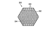
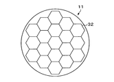
- the light emitting element unit 30 has a support plate 32 formed in a hexagonal shape as shown in FIG. 2, and a large number of light emitting elements 33 are arranged on the surface of the support plate 32.
- a light emitting diode (LED) is used as the light emitting element 33.
- the heat source 11 is configured so that the sides of the hexagonal support plate 32 of one light emitting element unit 30 are adjacent to each other. By setting it as such an arrangement structure, all the light emitting element units 30 are arrange
- the LED used as the light emitting element 33 a compound semiconductor such as GaN (gallium nitride) or GaAs (gallium arsenide) having a light wavelength in the range of ultraviolet to near infrared, preferably in the range of 360 to 1000 nm is used.
- the wafer W to be heated is a silicon wafer, and an LED made of a GaAs-based material having a wavelength near 880 nm, which is highly absorbed by the silicon wafer, is used.
- a power supply 40 for supplying a current to each light emitting element unit 30 is disposed on the top surface of the top plate 12b.
- the power source 40 is connected to a control unit 150 described later, and the current supplied to each light emitting element unit 30 is controlled by the control unit 150.
- a light transmitting member 50 that transmits light emitted from the light emitting element unit 30 toward the wafer W is separated from the upper surface of the cooling plate 10 by a predetermined distance between the cooling plate 10 and the light emitting element unit 30.
- the light transmissive member 50 for example, quartz or the like is used.
- the light transmitting member 50 is supported by a support member (not shown) provided on the side wall 12a of the processing container.
- a gas flow path 50 a is formed inside the light transmitting member 50.
- a plurality of openings are formed in the lower surface of the light transmission member 50, and the gas flow path 50a communicates with the openings.
- a processing gas supply pipe 52 for introducing a predetermined processing gas from the gas supply mechanism 51 and an exhaust pipe 54 connected to the exhaust mechanism 53 pass through the top plate 12 b in the processing container 12. Is provided.
- the processing gas supply pipe 52 communicates with a gas flow path 50 a formed inside the light transmission member 50. Therefore, the processing gas introduced from the gas supply mechanism 51 is supplied from the lower surface of the light transmission member 50 toward the upper surface of the wafer W.
- the exhaust pipe 54 communicates with the exhaust passage 50b formed inside the light transmission member 50 on the outer peripheral side of the gas passage 50a. Therefore, the processing gas introduced into the processing container 12 from the gas supply mechanism 51 via the gas flow path 50a forms an airflow that flows in a direction from the center of the wafer W toward the outer periphery.
- the processing gas supply pipe 52 is provided with a flow rate adjusting mechanism 55 that adjusts the flow rate of the processing gas introduced into the processing container 12. Further, the exhaust pipe 54 is provided with an exhaust adjustment mechanism 56 that adjusts the exhaust flow rate from the processing container 12.
- the substrate processing apparatus 1 described above is provided with a control unit 150 as shown in FIG.
- the control unit 150 is, for example, a computer and has a program storage unit (not shown).
- the program storage unit stores a program for controlling the processing of the wafer W in the substrate processing apparatus 1.
- the program storage unit also stores a program for controlling the operations of the power supply 40 and the lifting mechanism 21 to realize the heating process for the wafer W in the substrate processing apparatus 1.
- the program is recorded on a computer-readable storage medium such as a computer-readable hard disk (HD), flexible disk (FD), compact disk (CD), magnetic optical desk (MO), or memory card. Or installed in the control unit 150 from the storage medium.
- HD computer-readable hard disk
- FD flexible disk
- CD compact disk
- MO magnetic optical desk
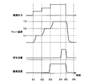
- FIG. 4 is a time chart showing the heat treatment conditions in the substrate processing apparatus 1.
- the horizontal axis in FIG. 4 represents time, and the vertical axis represents the power output, the temperature of the wafer W, the exhaust flow rate in the processing container 12, and the oxygen concentration.
- the shutter (not shown) of the processing container 12 is opened, and the wafer W is transferred above the support pins 20 by a transfer mechanism (not shown) provided outside the processing container 12.
- a predetermined pattern is formed in advance on the wafer W by using, for example, photolithography, and a coating liquid is further applied on the pattern.
- the coating solution an organic film as a resist underlayer film, more specifically, a solution for forming an SOC (Spin On Carbon) film is used.
- the support pins 20 are raised, and the wafer W is transferred from the transfer mechanism to the support pins 20.
- the shutter is then closed.
- oxygen gas is supplied from the gas supply mechanism 51 as a processing gas at a predetermined flow rate.
- the inside of the processing container 12 is exhausted by the exhaust mechanism 53.
- the supply amount of oxygen gas from the gas supply mechanism 51 is adjusted so that the oxygen concentration in the processing container 12 is 5% or less.
- the support pins 20 are raised until the distance between the wafer W and the light transmission member 50 reaches a predetermined distance, for example, 10 mm.
- a current is supplied from the power source 40 to each light emitting element unit of the heat source 11, and the wafer W is irradiated with light from the heat source 11 (time S1 in FIG. 4).
- the output of the power source 40 is adjusted so that the temperature of the wafer W is maintained at the first temperature T1 by irradiation of light from the heat source 11. 1st temperature T1 is more than the volatilization temperature of the solvent contained in a coating liquid.
- the heating time at the first temperature is set based on the time obtained by obtaining the time until the solvent volatilizes by a test performed in advance.
- the first temperature T1 is preferably not only higher than the volatilization temperature of the solvent in the coating liquid, but also preferably lower than the glass transition point of the coating liquid, and is higher than the volatilization temperature of the solvent and the volatilization temperature of the solvent. It is more preferable to set the temperature to not exceed 10 ° C. More preferably, the upper limit of the first temperature T1 is a temperature not exceeding the ignition point temperature of the solvent.
- the heating temperature low, the temperature in the processing container 12 can be prevented from becoming higher than the ignition point of the solvent. Further, although the solvent is volatilized even at normal temperature, the volatilization is promoted by heating at the first temperature T1, and the throughput of the heat treatment of the wafer W can be improved.
- the output of the power supply 40 is then increased (time S2 in FIG. 4), and the temperature of the wafer W is raised to the second temperature T2.
- the second temperature T2 is a temperature that is higher than the glass transition temperature of the coating solution and lower than the crosslinking start temperature of the coating solution.
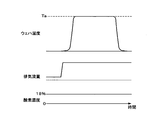
- a wafer is heat-treated under a temperature condition as shown in FIG. That is, the temperature of the wafer W is raised from room temperature to a predetermined temperature Ta, heat treatment is performed at that temperature for a certain time, and then the wafer W is cooled again to room temperature.
- the predetermined temperature Ta at this time is a temperature equal to or higher than the crosslinking temperature of the coating liquid applied to the wafer W.
- the exhaust flow rate is also kept constant, and the oxygen concentration in the treatment container is also kept constant at about 18%, which is slightly lower than the oxygen concentration in the air, for example.
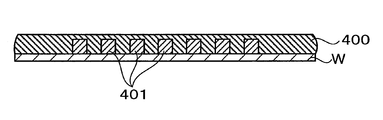
- the resist underlayer film 400 is maintained in a state where the step is maintained.
- the other steps formed on the upper layer of the resist underlayer film 400 are also affected by a step.
- the heat treatment is performed at the second temperature T2 that is higher than the glass transition point and lower than the crosslinking start temperature of the coating liquid in the period of time S2 to S3 in FIG.
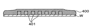
- the resist underlayer film which is a coating film, is fluidized by heating at a temperature equal to or higher than the glass transition point, and the resist underlayer film in which a step is generated is flattened as shown in FIG.
- the resist underlayer film 400 having a uniform height can be obtained without any problem.
- the fluidized resist underlayer film 400 may have a patchy pattern due to the influence of the air flow in the processing container 12. Therefore, the exhaust flow rate by the exhaust mechanism 53 is kept low during the period of heat treatment at the second temperature T2.
- the exhaust flow rate at this time varies depending on the properties of the resist underlayer film used, it can be obtained by conducting a test or the like in advance.
- the exhaust flow rate can be kept low in the heat treatment period at the first temperature T1 as in the heat treatment period at the second temperature T2. In such a case, it is preferable that the exhaust flow rate during the heat treatment period at the first temperature T1 is further suppressed to be lower than the exhaust flow rate during the heat treatment period at the second temperature T2.
- the third temperature T3 is a temperature that is equal to or higher than the crosslinking start temperature of the resist underlayer film 400 and lower than the decomposition temperature of the material constituting the resist underlayer film 400.
- the exhaust flow rate by the exhaust mechanism 53 is increased at time S4.
- Various sublimates are generated in the processing container from the coating film on the wafer W by the heat treatment of the wafer W. By increasing the exhaust flow rate, these sublimates are quickly discharged. For example, after the heat treatment is completed, the processing container When the 12 shutters are opened, it is possible to prevent the sublimate from diffusing outside the processing container 12. At this time, since the wafer W is cured by heat treatment at the third temperature T3, the resist underlayer film 400 on the wafer W is not affected by the airflow. Therefore, a patchy pattern does not occur in the resist underlayer film 400.
- the supply amount of oxygen gas as the processing gas is increased from the gas supply mechanism 51, and the oxygen concentration in the processing container 12 is set to a predetermined concentration, in this embodiment, the oxygen concentration in the atmosphere. Same or more, that is, about 20% or more.
- a predetermined concentration in this embodiment, the oxygen concentration in the atmosphere.
- the oxygen concentration is increased when the temperature is raised to the third temperature T3 which is the highest temperature in the heat treatment shown in FIG.
- the resist underlayer film 400 can be effectively oxidized.
- the oxidation reaction occurs by placing the resist underlayer film 400 in an oxygen atmosphere even at a low temperature, the oxidation reaction may or may not occur locally at a low temperature to perform uniform processing. I can't.
- the resist underlayer film 400 is fluidized at the time of the heat treatment at the second temperature T2 if the heat treatment is performed in a state where the oxygen concentration is high, an oxidation reaction is caused not only on the surface of the resist underlayer film 400 but also inside. Occur. As a result, the oxidized portion and the non-oxidized portion are generated inhomogeneously, and the film quality of the resist underlayer film 400 becomes inhomogeneous.
- the oxygen concentration is kept low to prevent a local oxidation reaction from occurring.
- the third temperature T3 in a state of being cured by heat treatment at the third temperature T3. Since the resist underlayer film 400 is oxidized at a high oxygen concentration, the vicinity of the surface of the resist underlayer film 400 can be uniformly oxidized. As a result, a uniform treatment can be performed over the entire surface of the resist underlayer film 400 to form the resist underlayer film 400 having a uniform film quality.
- the support pins 20 are then lowered, and the wafer W is placed on the cooling plate 10. Thereby, the wafer W is cooled to room temperature. At the same time, the supply amount of oxygen gas from the gas supply mechanism 51 is reduced. At that time, the exhaust flow rate by the exhaust mechanism 53 is also decreased. For example, when the wafer W reaches room temperature at time S6, the shutter of the processing container 12 is opened, and the wafer W is unloaded from the processing container 12 by the transport mechanism.
- the wafer W is carried into a coating processing apparatus provided outside the substrate processing apparatus 1, and a resist intermediate layer film is applied thereto.
- a resist intermediate layer film is formed without being affected by the pattern 401.
- a resist upper layer film is formed on the resist intermediate layer film, and then the wafer W is exposed.
- development processing and etching processing of the wafer W are sequentially performed, and a series of wafer processing ends.
- the solvent in the resist underlayer film 400 is first volatilized by heat treatment at the first temperature T1, and then the resist underlayer film 400 flows by heat treatment at the second temperature T2. Make it.
- the resist underlayer film 400 applied on the stepped wafer W is planarized.
- the resist underlayer film 400 after the planarization is subjected to a heat treatment at the third temperature T3, so that the resist underlayer film 400 is cured by crosslinking reaction.
- the resist underlayer film 400 having a uniform height can be formed without being affected by the pattern 401.
- a film having a uniform height can be formed without the influence of the pattern 401 on the film formed on the resist underlayer film 400.
- the temperature in the processing container 12 becomes more than the ignition point of a solvent by making 1st temperature T1 into the temperature which is more than the volatilization temperature of the solvent in the resist lower layer film 400, and does not exceed the ignition point of a solvent. Can be prevented.
- the oxygen concentration in the processing container 12 is maintained equal to or higher than the oxygen concentration in the air.
- the oxidation reaction of the resist underlayer film 400 can be promoted, and a coating film highly resistant to pattern collapse can be formed.
- the oxygen concentration is maintained at 5% or less during the heat treatment period at the first temperature T1 and the second temperature T2
- it is observed that the oxidation reaction occurs locally when the temperature of the wafer W is low.
- the resist underlayer film 400 cured by heat treatment at the third temperature T3 is oxidized at a high oxygen concentration, the vicinity of the surface of the resist underlayer film 400 can be uniformly oxidized.
- the oxygen concentration in the heat treatment at the third temperature T3 is more preferably 30% or more, but components other than the resist underlayer film 400 formed on the wafer W are excessively oxidized or corroded.
- the upper limit of the oxygen concentration is preferably 50% or less.
- the pattern collapse occurs when the line width of the resist pattern is 34.5 nm or less, whereas in the example, the line width is 31.3 nm.
- the pattern collapse did not occur until the following, and it was confirmed that the resistance to pattern collapse was improved by the method of the present embodiment.
- pattern collapse is caused by LER (Line Edge). Roughness) exceeding 4 nm was judged as having pattern collapse.
- the exhaust flow rate from the processing container 12 is increased after a predetermined time has elapsed from the heat treatment at the third temperature T3, that is, after the resist underlayer film 400 on the wafer W is cured by the crosslinking reaction. Therefore, the sublimate generated from the wafer W by the heat treatment can be quickly discharged without affecting the resist underlayer film 400 by the airflow.
- the exhaust flow rate from the processing container 12 is kept low, so that the resist lower layer film 400 before curing is caused by an air flow. Not affected. Therefore, it is possible to avoid the occurrence of a patchy pattern due to the influence of an air flow, for example, on the surface of the resist underlayer film 400.
- the LED is used as the heat source 11 when the wafer W is heat-treated.
- a heat plate used in a conventional heat treatment for example, an electric heater is built in, has a large time constant and does not immediately increase the temperature of the heat plate itself even when the output of the electric heater is increased.
- the temperature of the wafer W can be quickly raised.
- another wafer W is heat-treated after the wafer W is heat-treated using the hot plate at the third temperature T3, it is once cooled until the temperature of the hot plate becomes lower than the first temperature T1, for example. This requires a certain amount of time.
- a lamp heater such as a halogen heater may be used instead of the LED.
- the heating temperature of the wafer W is adjusted by changing the output of the power supply 40 while keeping the distance between the wafer W and the heat source 11 constant.
- the output of the power supply 40 is kept constant.
- the heating temperature of the wafer W may be adjusted by moving the support pins 20 up and down while changing the distance between the wafer W and the heat source 11.
- the present invention is not limited to such examples. It is obvious for those skilled in the art that various modifications or modifications can be conceived within the scope of the idea described in the claims, and these naturally belong to the technical scope of the present invention. It is understood.
- the present invention is not limited to this example and can take various forms.
- the present invention can also be applied to a case where the substrate is another substrate such as an FPD (flat panel display) other than a wafer or a mask reticle for a photomask.
- FPD flat panel display
- the present invention is useful when forming a coating film with few steps on a substrate having steps.
Landscapes
- Engineering & Computer Science (AREA)
- General Physics & Mathematics (AREA)
- Manufacturing & Machinery (AREA)
- Physics & Mathematics (AREA)
- Microelectronics & Electronic Packaging (AREA)
- Condensed Matter Physics & Semiconductors (AREA)
- Computer Hardware Design (AREA)
- Power Engineering (AREA)
- Toxicology (AREA)
- Health & Medical Sciences (AREA)
- Exposure Of Semiconductors, Excluding Electron Or Ion Beam Exposure (AREA)
- Coating Apparatus (AREA)
- Drying Of Semiconductors (AREA)
- Materials For Photolithography (AREA)
- Resistance Heating (AREA)
- Photosensitive Polymer And Photoresist Processing (AREA)
Abstract
段差を有するパターンが形成された基板に塗布膜を形成する方法であって、塗布液が塗布された基板を、当該塗布液の溶剤の揮発温度以上で且つガラス転移点より低い温度である第1の温度で加熱する第1の加熱工程と、塗布液のガラス転移点以上で且つ前記塗布液の架橋開始温度より低い第2の温度で基板を加熱する第2の加熱工程と、塗布液の架橋開始温度以上で且つ塗布膜の材料分解温度よりも低い第3の温度で基板を加熱して塗布膜を形成する第3の加熱工程と、を有し、基板の加熱は光の照射によって行う。
Description
本発明は、所定のパターンが形成されたことにより段差を有する基板上に塗布膜を形成する方法及びコンピュータ記憶媒体に関する。
本願は、2013年7月5日に日本国に出願された特願2013-141295号に基づき、優先権を主張し、その内容をここに援用する。
本願は、2013年7月5日に日本国に出願された特願2013-141295号に基づき、優先権を主張し、その内容をここに援用する。
例えば半導体デバイスの製造工程では、例えば半導体ウェハ(以下、「ウェハ」という。)上にレジスト液を塗布してレジスト膜を形成するレジスト塗布処理、当該レジスト膜に所定のパターンを露光する露光処理、露光されたレジスト膜を現像する現像処理などを順次行うフォトリソグラフィー処理が行われ、ウェハ上に所定のレジストパターンが形成される。そして、このレジストパターンをマスクとして、ウェハ上の被処理膜のエッチング処理が行われ、その後レジスト膜の除去処理などが行われて、被処理膜に所定のパターンが形成される。
近年、半導体デバイスのさらなる高集積化を図るため、上述した被処理膜のパターンの微細化が求められている。このため、レジストパターンの微細化が進められており、例えばフォトリソグラフィー処理における露光処理の光を短波長化することが進められている。
レジストパターンのアスペクト比が大きくなるほどレジストのパターン倒れが発生しやすくなる。そのため、パターン倒れを防ぐためには、レジストの膜厚は薄くする必要がある。しかしながら、膜厚の薄いレジストから形成されるレジストパターンは例えばドライエッチングに対する耐性が低く、エッチングの際に消失してしまう恐れがある。
そこで、パターン倒れを防ぎ、且つマスクとして良好に機能するレジストパターンを形成するために、レジストパターンの下地としてレジスト下層膜やレジスト中間層膜を形成する方法ことが、例えば特許文献1に開示されている。
特許文献1の方法においては、例えばウェハ上にレジスト下層膜を形成し、次いでレジスト下層膜上にレジスト中間層膜を形成する。その後、レジスト中間層膜上にフォトレジストをレジスト上層膜として形成する。そして、レジスト上層膜に露光、現像処理を行い、レジスト上層膜によりレジストパターンを形成する。
その後、このレジストパターンをマスクとしてレジスト中間層膜をエッチングしてパターンをレジスト中間層膜に転写する。次いで、レジスト中間層膜に転写されたパターンをマスクとして、レジスト下層膜をエッチングしてパターンをレジスト下層膜に転写する。これにより、膜厚の薄いレジストであってもエッチング耐性を有するマスクを形成できる。
ところで、半導体デバイスの製造工程においては、既に所定のパターンが形成されたウェハ上にさらにエッチングのマスクとしてレジストパターンの形成が行われる。かかる場合においても上述のような、多層の膜を用いたパターン形成方法が用いられる。
しかしながら、パターン形成後のウェハはパターンに応じた段差を有しているため、そのパターン上にレジスト下層膜を塗布すると、例えば図7に示すように、当該レジスト下層膜400にもウェハW上に形成されたパターン401の影響による段差が生じてしまう。そうすると、その後に塗布されるレジスト中間層膜及びレジスト上層膜にも段差が生じ、この段差がレジスト上層膜を露光処理する際にデフォーカスの原因になるという問題が生じている。
本発明は、かかる点に鑑みてなされたものであり、段差を有する基板上に塗布液を塗布して塗布膜を形成するにあたり、基板の段差の影響を抑えた段差の少ない塗布膜を形成することを目的とする。
前記の目的を達成するため、本発明は、段差を有するパターンが形成された基板に塗布膜を形成する方法であって、塗布液が塗布された基板を、当該塗布液の溶剤の揮発温度以上で且つガラス転移点より低い温度である第1の温度で加熱する第1の加熱工程と、前記塗布液のガラス転移点以上で且つ前記塗布液の架橋開始温度より低い第2の温度で前記基板を加熱する第2の加熱工程と、前記塗布液の架橋開始温度以上で且つ前記塗布膜の材料分解温度よりも低い第3の温度で前記基板を加熱して塗布膜を形成する第3の加熱工程と、を有し、前記基板の加熱は、前記基板に光を照射して行う。
本発明によれば、先ず第1の温度で加熱することで塗布液中の溶剤を揮発させる。次いで第2の温度で加熱することで塗布液を流動化させ、これにより段差を有する基板上に塗布された塗布液を平坦化する。そして、平坦化後の塗布液を第3の温度で加熱することで、塗布液を架橋反応させて硬化させる。これにより、基板に形成されていたパターンの影響を受けることなく、均一な高さの塗布膜を形成することができる。また、光を照射して加熱処理を行うので、速やかに基板を昇温でき、加熱処理のスループットを向上させることができる。
別な観点による本発明は、前記塗布膜の形成方法を基板処理装置によって実行させるように、当該基板処理装置を制御する制御部のコンピュータ上で動作するプログラムを格納した読み取り可能なコンピュータ記憶媒体である。
本発明によれば、段差を有する基板上に塗布液を塗布して塗布膜を形成するにあたり、基板の段差の影響を抑えた段差の少ない塗布膜を形成できる。
以下、本発明の実施の形態について説明する。図1は、本実施の形態にかかる塗布膜の形成方法を実施する基板処理装置1の構成の概略を示す縦断面図である。なお、本実施の形態に係る基板処理装置1は、例えばウェハWを加熱処理する熱処理装置である。また、本実施の形態において基板処理装置1で処理されるウェハWには、予め所定のパターンを有する膜が形成されている。
基板処理装置1は、ウェハWを載置して冷却する冷却板10とウェハWを加熱する熱源11が設けられた処理容器12を有している。処理容器12は、略円筒形状の側壁12a、側壁12aの上端を塞ぐ天板12b、及び側壁12aの下端を塞ぐ底板12cを有している。側壁12aと天板12bとの間、及び側壁12aと底板12cとの間には、それぞれ図示しないシール部材が設けられ、処理容器12は気密に形成されている。
冷却板10の下方には、ウェハWを支持する支持ピン20が複数設けられている。支持ピン20は、例えば処理容器12の外部に設けられた昇降機構21に接続されて昇降自在となっている。冷却板10には、支持ピン20が昇降する際に当該冷却板10との干渉を避けるため、貫通孔20aが複数形成されている。ウェハWは、加熱処理の際に熱源11と間の距離が所定の値となるように、支持ピン20によって持ち上げられる。
熱源11は、処理容器12の天板12bの下面に配置されている。熱源11は、複数の発光素子ユニット30により構成されている。各発光素子ユニット30は、支持ピン20に支持されたウェハWに光を照射するように、冷却板10に対向して設けられている。各発光素子ユニット30は、電極31を介して支持部材31aに支持され、支持部材31aは天板12bに支持されている。天板12bの内部には図示しない冷媒管が設けられ、その内部に冷却水を通水することで、発光素子ユニット30の冷却が行なわれる。
発光素子ユニット30は、図2に示すように六角状に形成された支持板32を有し、当該支持板32の表面に発光素子33が多数配置されている。発光素子33としては、例えば発光ダイオード(LED)が用いられる。そして、熱源11は、例えば図3に示すように、一つの発光素子ユニット30の六角状の支持板32の辺が互いに隣接するように配置されて構成されている。このような配置構成とすることで、全ての発光素子ユニット30が天板12bに均等に配置される。
発光素子33として用いられるLEDとしては、光の波長が紫外~近赤外の範囲、好ましくは360~1000nmの範囲の、例えばGaN(窒化ガリウム)やGaAs(ガリウムヒ素)などの化合物半導体が用いられる。なお、本実施の形態では、加熱対象であるウェハWがシリコン製のウェハであり、シリコンウェハによる吸収率の高い880nm付近の波長を有するGaAs系の材料からなるLEDを用いている。
天板12bの上面には、各発光素子ユニット30に電流を供給する電源40が配置されている。電源40は、後述する制御部150に接続されており各発光素子ユニット30へ供給する電流は制御部150により制御される。
冷却板10と発光素子ユニット30との間には、発光素子ユニット30からウェハWに向けて照射された光を透過する光透過部材50が、冷却板10の上面と所定の距離だけ離間して配置されている。光透過部材50としては、例えば石英などが用いられる。光透過部材50は、処理容器の側壁12aに設けられた支持部材(図示せず)により支持されている。光透過部材50の内部には、ガス流路50aが形成されている。また、光透過部材50の下面には開口が複数形成され、ガス流路50aは、この開口に連通している。
処理容器12には、当該処理容器12内に、ガス供給機構51から所定の処理ガスを導入する処理ガス供給管52と、排気機構53に接続された排気管54がそれぞれ天板12bを貫通して設けられている。
処理ガス供給管52は、光透過部材50の内部に形成されたガス流路50aに連通している。そのため、ガス供給機構51から導入された処理ガスは、光透過部材50の下面からウェハWの上面に向けて供給される。排気管54は、光透過部材50の内部に、ガス流路50aよりも外周部側に形成された排気流路50bに連通している。したがって、ガス供給機構51からガス流路50aを介して処理容器12内に導入された処理ガスは、ウェハWの中心から外周に向かう方向に流れる気流を形成する。
処理ガス供給管52には、処理容器12内に導入する処理ガスの流量を調節する流量調節機構55が設けられている。また、排気管54には、処理容器12からの排気流量を調節する排気調節機構56が設けられている。
以上の基板処理装置1には、図1に示すように制御部150が設けられている。制御部150は、例えばコンピュータであり、プログラム格納部(図示せず)を有している。プログラム格納部には、基板処理装置1におけるウェハWの処理を制御するプログラムが格納されている。また、プログラム格納部には、上述の電源40や昇降機構21の動作を制御して、基板処理装置1におけるウェハWの加熱処理を実現させるためのプログラムも格納されている。なお、前記プログラムは、例えばコンピュータ読み取り可能なハードディスク(HD)、フレキシブルディスク(FD)、コンパクトディスク(CD)、マグネットオプティカルデスク(MO)、メモリーカードなどのコンピュータに読み取り可能な記憶媒体に記録されていたものであって、その記憶媒体から制御部150にインストールされたものであってもよい。
次に、以上のように構成された基板処理装置1を用いて行われるウェハ処理、具体的には塗布液が塗布されたウェハWを加熱処理して塗布膜を形成する方法について、図4を用いて説明する。図4は、基板処理装置1における加熱処理条件を示すタイムチャートである。図4の横軸は時間、縦軸は電源出力、ウェハWの温度、処理容器12内の排気流量、酸素濃度を表している。
先ず、処理容器12のシャッタ(図示せず)が開き、ウェハWが処理容器12の外部に設けられた搬送機構(図示せず)によって支持ピン20の上方に搬送される。このウェハWには、上述の通り、予め例えばフォトリソグラフィーを用いて所定のパターンが形成されており、パターン上にはさらに塗布液が塗布されている。なお、塗布液としては、レジスト下層膜としての有機膜、より具体的にはSOC(Spin On Carbon)膜を形成するための溶液が用いられる。
次に、支持ピン20が上昇し、ウェハWが搬送機構から支持ピン20に受け渡される。ウェハWが支持ピン20に受け渡され、搬送機構が処理容器12から退避すると、次にシャッタが閉じられる。その後、ガス供給機構51から処理ガスとして酸素ガスが所定の流量で供給される。それと共に、排気機構53により処理容器12内が排気される。この際、ガス供給機構51からの酸素ガスの供給量は、処理容器12内の酸素濃度が5%以下になるように調節される。
次いで、ウェハWと光透過部材50と間の距離が所定の距離、例えば10mmになるまで支持ピン20が上昇する。次に、電源40から熱源11の各発光素子ユニットに電流が供給され、熱源11からウェハWに光が照射される(図4の時間S1)。この際、電源40の出力は、熱源11からの光の照射によりウェハWの温度が第1の温度T1に維持されるように調節される。第1の温度T1は、塗布液に含まれる溶剤の揮発温度以上である。この第1の温度でウェハWを所定の期間(図4の時間S1~S2の間)加熱することで、ウェハWに塗布された塗布液から溶剤が揮発する。第1の温度での加熱時間は、予め行われる試験により溶剤が揮発するまでの時間を求め、当該求められた時間に基づいて設定される。なお、第1の温度T1は、塗布液中の溶剤の揮発温度以上とするだけでなく、塗布液のガラス転移点以下の温度とすることが好ましく、溶剤の揮発温度以上で且つ溶剤の揮発温度を10℃以上超えない温度とすることがより好ましい。さらに好ましくは、第1の温度T1の上限は、溶剤の発火点温度を超えない温度である。加熱温度を低く抑えることで、処理容器12内の温度が溶剤の発火点以上となることを防ぐことができる。また、溶剤は常温でも揮発するが、第1の温度T1で加熱することで揮発を促進し、ウェハWの加熱処理のスループットを向上させることができる。
第1の温度T1での加熱処理が終了すると、次いで、電源40の出力を増加させ(図4の時間S2)、ウェハWの温度を第2の温度T2まで上昇させる。なお、第2の温度T2としては、塗布液のガラス転移点温度以上で且つ塗布液の架橋開始温度よりも低い温度である。この第2の温度T2でウェハWを所定の期間(図4の時間S2~S3の間)加熱することで、ウェハWに塗布された塗布液を流動化させ、ウェハWに塗布された塗布液を平坦化する。この塗布液の平坦化について具体的に説明する。
多層の膜を用いたパターン形成においては、従来、例えば図5に示すような温度条件でウェハの加熱処理が行われる。即ち、ウェハWを常温から所定の温度Taまで昇温し、その温度で一定時間加熱処理を行った後にウェハWを再び常温まで冷却する。この際の所定の温度Taは、ウェハWに塗布された塗布液の架橋温度以上の温度である。また、加熱処理の間は、排気流量も一定に保たれ、処理容器内の酸素濃度も例えば空気中の酸素濃度よりも若干低い約18%で一定に保たれる。ところが、図7に示すような、段差が生じた状態の、例えばレジスト下層膜400が形成されたウェハWを図5に示すような条件で加熱処理すると、段差が維持された状態でレジスト下層膜400が架橋反応し、レジスト下層膜400の上層に形成される他の膜にも段差の影響が生じてしまう。
そこで、本実施の形態では、図4の時間S2~S3の期間においては、ガラス転移点以上で且つ塗布液の架橋開始温度よりも低い温度である第2の温度T2で加熱処理を行う。ガラス転移点以上の温度で加熱することで塗布膜であるレジスト下層膜を流動化させ、段差が生じていたレジスト下層膜を図6に示すように平らにすることで、パターン401の影響を受けることなく均一な高さのレジスト下層膜400を得ることができる。なお流動化した状態のレジスト下層膜400には、処理容器12内の気流の影響により斑状の模様が生じる恐れがある。したがって、第2の温度T2で加熱処理する期間は、排気機構53による排気流量は低く抑えられる。この際の排気流量は、用いられるレジスト下層膜の性質により異なるので、予め試験等を行って求められる。なお、レジスト下層膜400への気流の影響を考慮し、第1の温度T1による加熱処理の期間においても、排気流量は第2の温度T2における加熱処理の期間と同様に低く抑えられる。かかる場合、第1の温度T1による加熱処理の期間における排気流量は、第2の温度T2における加熱処理の期間における排気流量よりもさらに低く抑えることが好ましい。
第2の温度T2での加熱処理が終了すると、次いで、電源40の出力を増加させ(図4の時間S3)、ウェハWの温度を第3の温度T3まで上昇させる。第3の温度T3は、レジスト下層膜400の架橋開始温度以上で且つレジスト下層膜400を構成する材料の分解温度よりも低い温度である。この第3の温度T3でウェハWを所定の期間(図4の時間S3~S5の間)加熱することで、架橋反応によりレジスト下層膜400を硬化させ、安定した膜を形成することができる。
また、時間S3から所定の時間経過後、時間S4において排気機構53による排気流量を増加させる。ウェハWの加熱処理によりウェハW上の塗布膜から様々な昇華物が処理容器内に発生するが、排気流量を増加させることでこれらの昇華物を速やかに排出し、例えば加熱処理終了後に処理容器12のシャッタを開放する際に、処理容器12の外部に昇華物が拡散することを防止できる。この際、ウェハWは第3の温度T3で加熱処理されることにより硬化しているので、ウェハW上のレジスト下層膜400は気流の影響をうけない。したがって、レジスト下層膜400に斑状の模様が生じることもない。
また、時間S3においては、ガス供給機構51から処理ガスとしての酸素ガスの供給量を増加させ、処理容器12内の酸素濃度を所定の濃度、本実施の形態においては、大気中の酸素濃度と同じか又はそれ以上、即ち約20%以上にする。例えば、フォトリソグラフィーに用いられるレジスト膜を加熱処理すると、架橋反応と共に酸化反応がおこり、この酸化反応を促進させることで、レジストパターンのパターン倒れに対する耐性が向上することが知られている。そして、加熱処理の際の温度が高いほど酸化反応は進む。そこで、本実施の形態においては、図4に示す加熱処理において最も高い温度である第3の温度T3に昇温する際に酸素濃度を増加させる。そうすることで、効果的にレジスト下層膜400を酸化させることができる。また、温度が低い状態でもレジスト下層膜400を酸素雰囲気中におくことで酸化反応は起こるが、温度が低い状態では、局所的に酸化反応が起こったり起こらなかったりして均一な処理を行うことができない。特に、第2の温度T2での加熱処理時はレジスト下層膜400が流動化しているため、酸素濃度が高い状態で加熱処理を行うと、レジスト下層膜400の表面のみではなく内部まで酸化反応が起こる。その結果、酸化される部分と酸化されない部分が不均質に生じ、レジスト下層膜400の膜質が不均質になってしまう。そのため、本実施の形態のように、低温状態では酸素濃度を低く保つことで局所的に酸化反応が起こることを防止し、その一方で、第3の温度T3での加熱処理により硬化した状態のレジスト下層膜400を高い酸素濃度で酸化させるので、レジスト下層膜400の表面近傍を均質に酸化させることができる。これにより、レジスト下層膜400の全面にわたって均一な処理を行い、均一な膜質のレジスト下層膜400を形成することができる。
時間S3~S5の期間、第3の温度T3で加熱処理が行われると、次いで、支持ピン20が下降し、ウェハWが冷却板10上に載置される。これによりウェハWは常温まで冷却される。またそれと共に、ガス供給機構51からの酸素ガスの供給量を減少させる。その際、排気機構53による排気流量も減少させる。そして、例えば時間S6においてウェハWが常温に達すると、処理容器12のシャッタが開き、搬送機構によりウェハWが処理容器12から搬出される。
その後ウェハWは、基板処理装置1の外部に設けられた塗布処理装置に搬入され、レジスト中間層膜が塗布される。この際、基板処理装置1での加熱処理によりレジスト下層膜400が平坦化されているので、パターン401の影響を受けることなく平坦なレジスト中間層膜が形成される。その後、レジスト中間層膜上にレジスト上層膜が形成され、次いでウェハWが露光処理される。その後、ウェハWの現像処理、エッチング処理が順次行われ、一連のウェハ処理が終了する
以上の実施の形態によれば、先ず第1の温度T1で加熱処理することでレジスト下層膜400中の溶剤を揮発させ、次いで第2の温度T2で加熱処理することでレジスト下層膜400を流動化させる。これにより段差を有するウェハW上に塗布されたレジスト下層膜400が平坦化される。そして、平坦化後のレジスト下層膜400を第3の温度T3で加熱処理することで、レジスト下層膜400を架橋反応させて硬化させる。これにより、パターン401の影響を受けることなく、均一な高さのレジスト下層膜400を形成することができる。その結果、レジスト下層膜400の上層に形成される膜にパターン401の影響を与えることなく、均一な高さの膜を形成することができる。
また、第1の温度T1を、レジスト下層膜400中の溶剤の揮発温度以上で且つ溶剤の発火点を超えない温度とすることで、処理容器12内の温度が溶剤の発火点以上となることを防ぐことができる。
また、以上の実施の形態では、第3の温度T3で加熱処理する際に、処理容器12中の酸素濃度を空気中の酸素濃度と同じかそれ以上に維持するので、第3の温度T3での加熱処理においてレジスト下層膜400の酸化反応を促進し、パターン倒れに対して耐性の高い塗布膜を形成することができる。また、第1の温度T1及び第2の温度T2での加熱処理の期間は酸素濃度を5%以下に維持しているので、ウェハWの温度が低い状態で局所的に酸化反応が起こることを防止し、その一方で、第3の温度T3での加熱処理により硬化した状態のレジスト下層膜400を高い酸素濃度で酸化させるので、レジスト下層膜400の表面近傍を均質に酸化させることができる。したがって、レジスト下層膜400の全面にわたって均一な処理を行い、均一な膜質のレジスト下層膜400を形成することができる。なお、第3の温度T3での加熱処理における酸素濃度は、30%以上とすることがより好ましいが、ウェハW上に構成されたレジスト下層膜400以外の構成物が過剰に酸化したり、腐食したりすることがないように、酸素濃度の上限は50%以下とすることが好ましい。
なお、本発明者らが、図5に示す従来のような条件で加熱処理を行った場合(比較例)と、図4に示す本実施の形態の条件で加熱処理を行った場合(実施例)について、パターン倒れに対する耐性を比較したところ、比較例においては、例えばレジストパターンの線幅が34.5nm以下においてパターン倒れが発生するのに対して、実施例においては、線幅が31.3nm以下となるまでパターン倒れが生じず、本実施の形態の方法により、パターン倒れに対する耐性が向上していることが確認された。なお、パターン倒れは、LER(Line Edge
Roughness)が4nmを超えたものをパターン倒れ有りと判定した。
Roughness)が4nmを超えたものをパターン倒れ有りと判定した。
以上の実施の形態では、第3の温度T3での加熱処理から所定の時間経過後、即ち、ウェハW上のレジスト下層膜400が架橋反応により硬化した後に処理容器12からの排気流量を増加させるので、レジスト下層膜400に気流による影響を与えることなく、加熱処理によりウェハWから発生した昇華物を速やかに排出することができる。
また、以上の実施の形態では、第1の温度T1及び第2の温度T2で加熱処理する際に、処理容器12からの排気流量を低く抑えるので、硬化する前のレジスト下層膜400が気流により影響を受けることがない。したがって、レジスト下層膜400の表面に、例えば気流の影響による斑状の模様が生じるといったことを避けることができる。
以上の実施の形態では、ウェハWを加熱処理する際の熱源11として、LEDを用いている。例えば、従来の加熱処理に用いる、例えば電気ヒータが内蔵された熱板は、時定数が大きく電気ヒータの出力を増加させても直ちに熱板そのものの温度が上昇しないが、本実施の形態のようにLEDを用いることで、速やかにウェハWを昇温させることができる。また、熱板を用いてウェハWを第3の温度T3で加熱処理した後に、別のウェハWを加熱処理する場合、熱板の温度が例えば第1の温度T1よりも低くなるまで一旦冷却する必要があり、そのために所定の時間を要するが、LEDを用いる場合はそのような冷却時間は不要であるため、ウェハW処理のスループットを向上させることができる。なお、熱源11としては、LEDに代えて、例えばハロゲンヒータのようなランプヒータを用いてもよい。
なお、以上の実施の形態では、ウェハWと熱源11との距離を一定に保った状態で、電源40の出力を変更してウェハWの加熱温度を調節したが、例えば電源40の出力を一定に保った状態で支持ピン20を昇降させ、ウェハWと熱源11との距離を変えることでウェハWの加熱温度を調節してもよい。
以上、添付図面を参照しながら本発明の好適な実施の形態について説明したが、本発明はかかる例に限定されない。当業者であれば、特許請求の範囲に記載された思想の範疇内において、各種の変更例または修正例に想到し得ることは明らかであり、それらについても当然に本発明の技術的範囲に属するものと了解される。本発明はこの例に限らず種々の態様を採りうるものである。本発明は、基板がウェハ以外のFPD(フラットパネルディスプレイ)、フォトマスク用のマスクレチクルなどの他の基板である場合にも適用できる。
本発明は、段差を有する基板上に、段差の少ない塗布膜を形成する際に有用である。
1 基板処理装置
10 冷却板
11 熱源
12 処理容器
20 支持ピン
21 昇降機構
30 発光素子ユニット
31 電極
32 支持板
40 電源
50 光透過部材
51 ガス供給機構
52 ガス供給管
53 排気機構
54 排気管
400 レジスト下層膜
401 パターン
W ウェハ
10 冷却板
11 熱源
12 処理容器
20 支持ピン
21 昇降機構
30 発光素子ユニット
31 電極
32 支持板
40 電源
50 光透過部材
51 ガス供給機構
52 ガス供給管
53 排気機構
54 排気管
400 レジスト下層膜
401 パターン
W ウェハ
Claims (9)
- 段差を有するパターンが形成された基板に塗布膜を形成する方法であって、
塗布液が塗布された基板を、当該塗布液の溶剤の揮発温度以上で且つガラス転移点より低い温度である第1の温度で加熱する第1の加熱工程と、
前記塗布液のガラス転移点以上で且つ前記塗布液の架橋開始温度より低い第2の温度で前記基板を加熱する第2の加熱工程と、
前記塗布液の架橋開始温度以上で且つ前記塗布膜の材料分解温度よりも低い第3の温度で前記基板を加熱して塗布膜を形成する第3の加熱工程と、を有し、
前記基板の加熱は、前記基板に光を照射して行う。 - 請求項1に記載の塗布膜の形成方法において、
前記第1の加熱工程及び前記第2の加熱工程は、前記第3の加熱工程よりも低酸素濃度雰囲気下で行う。 - 請求項2に記載の塗布膜の形成方法において、
前記第3の加熱工程は酸素濃度20%以上で50%以下の雰囲気下で行う。 - 請求項2に記載の塗布膜の形成方法において、
前記第1の加熱工程及び前記第2の加熱工程は酸素濃度5%以下の雰囲気下で行う。 - 請求項1に記載の塗布膜の形成方法において、
前記基板の加熱は、所定流量で排気される処理容器内で行い、前記第3の加熱工程における排気流量は、前記第1の加熱工程及び前記第2の加熱工程における排気流量よりも大きい。 - 請求項5に記載の塗布膜の形成方法において、
前記第1の加熱工程における排気流量は、前記第2の加熱工程における排気流量よりも小さい。 - 請求項1に記載の塗布膜の形成方法において、
前記基板への光の照射は、LEDまたはランプヒータにより行われる。 - 請求項1に記載の塗布膜の形成方法において、
前記塗布膜は、SOC膜である。 - 段差を有するパターンが形成された基板に塗布膜を形成する塗布膜の形成方法を、基板処理装置によって実行させるように当該基板処理装置を制御する制御部のコンピュータ上で動作するプログラムを格納した読み取り可能なコンピュータ記憶媒体であって、
前記塗布膜の形成方法は、
塗布液が塗布された基板を、当該塗布液の溶剤の揮発温度以上で且つガラス転移点より低い温度である第1の温度で加熱する第1の加熱工程と、
前記塗布液のガラス転移点以上で且つ前記塗布液の架橋開始温度より低い第2の温度で前記基板を加熱する第2の加熱工程と、
前記塗布液の架橋開始温度以上で且つ前記塗布膜の材料分解温度よりも低い第3の温度で前記基板を加熱して塗布膜を形成する第3の加熱工程と、を有し、
前記基板の加熱は、前記基板に光を照射して行う。
Applications Claiming Priority (2)
| Application Number | Priority Date | Filing Date | Title |
|---|---|---|---|
| JP2013141295A JP6081879B2 (ja) | 2013-07-05 | 2013-07-05 | 塗布膜の形成方法、プログラム及びコンピュータ記憶媒体 |
| JP2013-141295 | 2013-07-05 |
Publications (1)
| Publication Number | Publication Date |
|---|---|
| WO2015001936A1 true WO2015001936A1 (ja) | 2015-01-08 |
Family
ID=52143519
Family Applications (1)
| Application Number | Title | Priority Date | Filing Date |
|---|---|---|---|
| PCT/JP2014/065576 WO2015001936A1 (ja) | 2013-07-05 | 2014-06-12 | 塗布膜の形成方法及びコンピュータ記憶媒体 |
Country Status (3)
| Country | Link |
|---|---|
| JP (1) | JP6081879B2 (ja) |
| TW (1) | TWI569463B (ja) |
| WO (1) | WO2015001936A1 (ja) |
Families Citing this family (2)
| Publication number | Priority date | Publication date | Assignee | Title |
|---|---|---|---|---|
| WO2016125408A1 (ja) * | 2015-02-05 | 2016-08-11 | 東京エレクトロン株式会社 | 研磨装置、塗布膜形成装置、塗布膜形成方法、記憶媒体、パターン形成方法及びパターン形成装置 |
| JP7308671B2 (ja) * | 2019-07-03 | 2023-07-14 | 東京エレクトロン株式会社 | 基板熱処理装置、基板熱処理方法及び記憶媒体 |
Citations (6)
| Publication number | Priority date | Publication date | Assignee | Title |
|---|---|---|---|---|
| JPS6381820A (ja) * | 1986-09-25 | 1988-04-12 | Toshiba Corp | レジストパタ−ン形成方法 |
| JPS6381923A (ja) * | 1986-09-26 | 1988-04-12 | Hitachi Ltd | 感光性ポリイミド樹脂処理方法および装置 |
| JPH0289059A (ja) * | 1988-09-26 | 1990-03-29 | Hitachi Electron Eng Co Ltd | ベーク方法 |
| JPH0561206A (ja) * | 1991-08-30 | 1993-03-12 | Oki Electric Ind Co Ltd | レジストの平坦化方法 |
| JP2001188357A (ja) * | 1999-12-28 | 2001-07-10 | Matsushita Electric Ind Co Ltd | 表示素子用基板への樹脂膜形成法及び装置、並びに該方法を用いた液晶表示装置の製造方法 |
| JP2008186934A (ja) * | 2007-01-29 | 2008-08-14 | Dainippon Screen Mfg Co Ltd | 熱処理装置および熱処理方法 |
Family Cites Families (7)
| Publication number | Priority date | Publication date | Assignee | Title |
|---|---|---|---|---|
| JP3282240B2 (ja) * | 1992-10-03 | 2002-05-13 | 住友金属工業株式会社 | 帯状材の連続塗装方法 |
| JP3563434B2 (ja) * | 1994-03-22 | 2004-09-08 | 株式会社神戸製鋼所 | 感熱自己接着性樹脂塗装金属板およびその製法並びに該樹脂塗装金属板の接合法 |
| JP3801271B2 (ja) * | 1996-08-30 | 2006-07-26 | 旭硝子株式会社 | アクティブマトリクス基板 |
| US7495046B2 (en) * | 2001-12-17 | 2009-02-24 | Daikin Industries, Ltd. | Crosslinkable elastomer composition and formed product comprising the same |
| JP2004002752A (ja) * | 2002-03-28 | 2004-01-08 | Toray Ind Inc | ポリ(脂環式オレフィン)組成物の処理方法並びに半導体装置、光学部品および有機電界発光装置 |
| US20040084774A1 (en) * | 2002-11-02 | 2004-05-06 | Bo Li | Gas layer formation materials |
| KR101068372B1 (ko) * | 2005-07-05 | 2011-09-28 | 히다치 가세고교 가부시끼가이샤 | 감광성 접착제, 및 이것을 이용하여 얻어지는 접착 필름, 접착 시트, 접착제층 부착 반도체 웨이퍼, 반도체장치 및 전자부품 |
-
2013
- 2013-07-05 JP JP2013141295A patent/JP6081879B2/ja active Active
-
2014
- 2014-06-12 WO PCT/JP2014/065576 patent/WO2015001936A1/ja active Application Filing
- 2014-06-25 TW TW103121878A patent/TWI569463B/zh active
Patent Citations (6)
| Publication number | Priority date | Publication date | Assignee | Title |
|---|---|---|---|---|
| JPS6381820A (ja) * | 1986-09-25 | 1988-04-12 | Toshiba Corp | レジストパタ−ン形成方法 |
| JPS6381923A (ja) * | 1986-09-26 | 1988-04-12 | Hitachi Ltd | 感光性ポリイミド樹脂処理方法および装置 |
| JPH0289059A (ja) * | 1988-09-26 | 1990-03-29 | Hitachi Electron Eng Co Ltd | ベーク方法 |
| JPH0561206A (ja) * | 1991-08-30 | 1993-03-12 | Oki Electric Ind Co Ltd | レジストの平坦化方法 |
| JP2001188357A (ja) * | 1999-12-28 | 2001-07-10 | Matsushita Electric Ind Co Ltd | 表示素子用基板への樹脂膜形成法及び装置、並びに該方法を用いた液晶表示装置の製造方法 |
| JP2008186934A (ja) * | 2007-01-29 | 2008-08-14 | Dainippon Screen Mfg Co Ltd | 熱処理装置および熱処理方法 |
Also Published As
| Publication number | Publication date |
|---|---|
| JP6081879B2 (ja) | 2017-02-15 |
| JP2015015370A (ja) | 2015-01-22 |
| TWI569463B (zh) | 2017-02-01 |
| TW201517297A (zh) | 2015-05-01 |
Similar Documents
| Publication | Publication Date | Title |
|---|---|---|
| JP4438008B2 (ja) | 基板処理装置 | |
| JP5193121B2 (ja) | レジスト塗布現像方法 | |
| US9558960B2 (en) | Substrate processing method, non-transitory storage medium and heating apparatus | |
| KR20220031649A (ko) | 금속-함유 레지스트의 리소그래피 성능을 향상시키기 위한 소성 (bake) 전략들 | |
| JP2006060228A (ja) | ウェハベーキング装置 | |
| JP2018107175A (ja) | 熱処理装置、熱処理方法及びコンピュータ記憶媒体 | |
| JP5673523B2 (ja) | 基板処理方法、基板処理装置及び記憶媒体 | |
| JP6081879B2 (ja) | 塗布膜の形成方法、プログラム及びコンピュータ記憶媒体 | |
| JP2008192844A (ja) | 基板処理方法及び塗布現像処理装置 | |
| JP4965925B2 (ja) | 基板の処理システム | |
| JP6293645B2 (ja) | 基板処理システム | |
| JP2017117852A (ja) | 熱処理装置、基板を熱処理する方法及びコンピュータ読み取り可能な記録媒体 | |
| KR100626395B1 (ko) | 노광 후 베이크 장치 및 노광 후 베이크 방법, 그리고 상기장치를 가지는 포토 리소그래피 시스템 | |
| KR102498192B1 (ko) | 기판 처리 방법, 프로그램, 컴퓨터 기억 매체 및 기판 처리 시스템 | |
| KR100710705B1 (ko) | 기판 애싱 방법 | |
| WO2015115166A1 (ja) | 基板処理システム、基板処理方法及びコンピュータ記憶媒体 | |
| JP2009016657A (ja) | レジストパターンの再形成方法 | |
| KR100741578B1 (ko) | 반도체 제조를 위한 감광제 도포용 트랙장비의 핫 플레이트및 cd조절 방법 | |
| WO2022196259A1 (ja) | 基板処理方法及び基板処理装置 | |
| JP4202962B2 (ja) | 基板処理方法及び半導体装置の製造方法 | |
| KR20240026997A (ko) | 기판 처리 방법 및 기판 처리 시스템 | |
| JP4601514B2 (ja) | レジストパターンの形成方法 | |
| KR20060012468A (ko) | 반도체 노광 설비의 베이킹 장치 | |
| JP2005166999A (ja) | 基板の処理方法及び基板の露光時の露光量又は焦点位置の変動による基板の処理への影響を低減する方法 | |
| JP2016086042A (ja) | 基板処理方法、プログラム、コンピュータ記憶媒体及び基板処理システム |
Legal Events
| Date | Code | Title | Description |
|---|---|---|---|
| 121 | Ep: the epo has been informed by wipo that ep was designated in this application |
Ref document number: 14820082 Country of ref document: EP Kind code of ref document: A1 |
|
| NENP | Non-entry into the national phase |
Ref country code: DE |
|
| 122 | Ep: pct application non-entry in european phase |
Ref document number: 14820082 Country of ref document: EP Kind code of ref document: A1 |