WO2014203425A1 - Brasure sans plomb à base de zn et module d'alimentation à semi-conducteurs - Google Patents
Brasure sans plomb à base de zn et module d'alimentation à semi-conducteurs Download PDFInfo
- Publication number
- WO2014203425A1 WO2014203425A1 PCT/JP2013/083448 JP2013083448W WO2014203425A1 WO 2014203425 A1 WO2014203425 A1 WO 2014203425A1 JP 2013083448 W JP2013083448 W JP 2013083448W WO 2014203425 A1 WO2014203425 A1 WO 2014203425A1
- Authority
- WO
- WIPO (PCT)
- Prior art keywords
- melting point
- solder
- free solder
- based lead
- temperature
- Prior art date
Links
Images


Classifications
-
- B—PERFORMING OPERATIONS; TRANSPORTING
- B23—MACHINE TOOLS; METAL-WORKING NOT OTHERWISE PROVIDED FOR
- B23K—SOLDERING OR UNSOLDERING; WELDING; CLADDING OR PLATING BY SOLDERING OR WELDING; CUTTING BY APPLYING HEAT LOCALLY, e.g. FLAME CUTTING; WORKING BY LASER BEAM
- B23K35/00—Rods, electrodes, materials, or media, for use in soldering, welding, or cutting
- B23K35/22—Rods, electrodes, materials, or media, for use in soldering, welding, or cutting characterised by the composition or nature of the material
- B23K35/24—Selection of soldering or welding materials proper
- B23K35/28—Selection of soldering or welding materials proper with the principal constituent melting at less than 950 degrees C
- B23K35/282—Zn as the principal constituent
-
- B—PERFORMING OPERATIONS; TRANSPORTING
- B23—MACHINE TOOLS; METAL-WORKING NOT OTHERWISE PROVIDED FOR
- B23K—SOLDERING OR UNSOLDERING; WELDING; CLADDING OR PLATING BY SOLDERING OR WELDING; CUTTING BY APPLYING HEAT LOCALLY, e.g. FLAME CUTTING; WORKING BY LASER BEAM
- B23K35/00—Rods, electrodes, materials, or media, for use in soldering, welding, or cutting
- B23K35/22—Rods, electrodes, materials, or media, for use in soldering, welding, or cutting characterised by the composition or nature of the material
- B23K35/24—Selection of soldering or welding materials proper
- B23K35/28—Selection of soldering or welding materials proper with the principal constituent melting at less than 950 degrees C
-
- C—CHEMISTRY; METALLURGY
- C22—METALLURGY; FERROUS OR NON-FERROUS ALLOYS; TREATMENT OF ALLOYS OR NON-FERROUS METALS
- C22C—ALLOYS
- C22C18/00—Alloys based on zinc
-
- H—ELECTRICITY
- H01—ELECTRIC ELEMENTS
- H01L—SEMICONDUCTOR DEVICES NOT COVERED BY CLASS H10
- H01L23/00—Details of semiconductor or other solid state devices
- H01L23/28—Encapsulations, e.g. encapsulating layers, coatings, e.g. for protection
- H01L23/31—Encapsulations, e.g. encapsulating layers, coatings, e.g. for protection characterised by the arrangement or shape
- H01L23/3157—Partial encapsulation or coating
- H01L23/3171—Partial encapsulation or coating the coating being directly applied to the semiconductor body, e.g. passivation layer
-
- H—ELECTRICITY
- H01—ELECTRIC ELEMENTS
- H01L—SEMICONDUCTOR DEVICES NOT COVERED BY CLASS H10
- H01L24/00—Arrangements for connecting or disconnecting semiconductor or solid-state bodies; Methods or apparatus related thereto
- H01L24/01—Means for bonding being attached to, or being formed on, the surface to be connected, e.g. chip-to-package, die-attach, "first-level" interconnects; Manufacturing methods related thereto
- H01L24/02—Bonding areas ; Manufacturing methods related thereto
- H01L24/07—Structure, shape, material or disposition of the bonding areas after the connecting process
- H01L24/08—Structure, shape, material or disposition of the bonding areas after the connecting process of an individual bonding area
-
- H—ELECTRICITY
- H01—ELECTRIC ELEMENTS
- H01L—SEMICONDUCTOR DEVICES NOT COVERED BY CLASS H10
- H01L24/00—Arrangements for connecting or disconnecting semiconductor or solid-state bodies; Methods or apparatus related thereto
- H01L24/01—Means for bonding being attached to, or being formed on, the surface to be connected, e.g. chip-to-package, die-attach, "first-level" interconnects; Manufacturing methods related thereto
- H01L24/26—Layer connectors, e.g. plate connectors, solder or adhesive layers; Manufacturing methods related thereto
- H01L24/28—Structure, shape, material or disposition of the layer connectors prior to the connecting process
- H01L24/29—Structure, shape, material or disposition of the layer connectors prior to the connecting process of an individual layer connector
-
- H—ELECTRICITY
- H01—ELECTRIC ELEMENTS
- H01L—SEMICONDUCTOR DEVICES NOT COVERED BY CLASS H10
- H01L24/00—Arrangements for connecting or disconnecting semiconductor or solid-state bodies; Methods or apparatus related thereto
- H01L24/73—Means for bonding being of different types provided for in two or more of groups H01L24/10, H01L24/18, H01L24/26, H01L24/34, H01L24/42, H01L24/50, H01L24/63, H01L24/71
-
- H—ELECTRICITY
- H01—ELECTRIC ELEMENTS
- H01L—SEMICONDUCTOR DEVICES NOT COVERED BY CLASS H10
- H01L24/00—Arrangements for connecting or disconnecting semiconductor or solid-state bodies; Methods or apparatus related thereto
- H01L24/80—Methods for connecting semiconductor or other solid state bodies using means for bonding being attached to, or being formed on, the surface to be connected
- H01L24/83—Methods for connecting semiconductor or other solid state bodies using means for bonding being attached to, or being formed on, the surface to be connected using a layer connector
-
- H—ELECTRICITY
- H01—ELECTRIC ELEMENTS
- H01L—SEMICONDUCTOR DEVICES NOT COVERED BY CLASS H10
- H01L2224/00—Indexing scheme for arrangements for connecting or disconnecting semiconductor or solid-state bodies and methods related thereto as covered by H01L24/00
- H01L2224/01—Means for bonding being attached to, or being formed on, the surface to be connected, e.g. chip-to-package, die-attach, "first-level" interconnects; Manufacturing methods related thereto
- H01L2224/02—Bonding areas; Manufacturing methods related thereto
- H01L2224/04—Structure, shape, material or disposition of the bonding areas prior to the connecting process
- H01L2224/04042—Bonding areas specifically adapted for wire connectors, e.g. wirebond pads
-
- H—ELECTRICITY
- H01—ELECTRIC ELEMENTS
- H01L—SEMICONDUCTOR DEVICES NOT COVERED BY CLASS H10
- H01L2224/00—Indexing scheme for arrangements for connecting or disconnecting semiconductor or solid-state bodies and methods related thereto as covered by H01L24/00
- H01L2224/01—Means for bonding being attached to, or being formed on, the surface to be connected, e.g. chip-to-package, die-attach, "first-level" interconnects; Manufacturing methods related thereto
- H01L2224/02—Bonding areas; Manufacturing methods related thereto
- H01L2224/04—Structure, shape, material or disposition of the bonding areas prior to the connecting process
- H01L2224/05—Structure, shape, material or disposition of the bonding areas prior to the connecting process of an individual bonding area
- H01L2224/0554—External layer
- H01L2224/05599—Material
- H01L2224/056—Material with a principal constituent of the material being a metal or a metalloid, e.g. boron [B], silicon [Si], germanium [Ge], arsenic [As], antimony [Sb], tellurium [Te] and polonium [Po], and alloys thereof
- H01L2224/05617—Material with a principal constituent of the material being a metal or a metalloid, e.g. boron [B], silicon [Si], germanium [Ge], arsenic [As], antimony [Sb], tellurium [Te] and polonium [Po], and alloys thereof the principal constituent melting at a temperature of greater than or equal to 400°C and less than 950°C
- H01L2224/05618—Zinc [Zn] as principal constituent
-
- H—ELECTRICITY
- H01—ELECTRIC ELEMENTS
- H01L—SEMICONDUCTOR DEVICES NOT COVERED BY CLASS H10
- H01L2224/00—Indexing scheme for arrangements for connecting or disconnecting semiconductor or solid-state bodies and methods related thereto as covered by H01L24/00
- H01L2224/01—Means for bonding being attached to, or being formed on, the surface to be connected, e.g. chip-to-package, die-attach, "first-level" interconnects; Manufacturing methods related thereto
- H01L2224/02—Bonding areas; Manufacturing methods related thereto
- H01L2224/04—Structure, shape, material or disposition of the bonding areas prior to the connecting process
- H01L2224/05—Structure, shape, material or disposition of the bonding areas prior to the connecting process of an individual bonding area
- H01L2224/0554—External layer
- H01L2224/05599—Material
- H01L2224/056—Material with a principal constituent of the material being a metal or a metalloid, e.g. boron [B], silicon [Si], germanium [Ge], arsenic [As], antimony [Sb], tellurium [Te] and polonium [Po], and alloys thereof
- H01L2224/05638—Material with a principal constituent of the material being a metal or a metalloid, e.g. boron [B], silicon [Si], germanium [Ge], arsenic [As], antimony [Sb], tellurium [Te] and polonium [Po], and alloys thereof the principal constituent melting at a temperature of greater than or equal to 950°C and less than 1550°C
- H01L2224/05644—Gold [Au] as principal constituent
-
- H—ELECTRICITY
- H01—ELECTRIC ELEMENTS
- H01L—SEMICONDUCTOR DEVICES NOT COVERED BY CLASS H10
- H01L2224/00—Indexing scheme for arrangements for connecting or disconnecting semiconductor or solid-state bodies and methods related thereto as covered by H01L24/00
- H01L2224/01—Means for bonding being attached to, or being formed on, the surface to be connected, e.g. chip-to-package, die-attach, "first-level" interconnects; Manufacturing methods related thereto
- H01L2224/02—Bonding areas; Manufacturing methods related thereto
- H01L2224/04—Structure, shape, material or disposition of the bonding areas prior to the connecting process
- H01L2224/06—Structure, shape, material or disposition of the bonding areas prior to the connecting process of a plurality of bonding areas
- H01L2224/061—Disposition
- H01L2224/0618—Disposition being disposed on at least two different sides of the body, e.g. dual array
- H01L2224/06181—On opposite sides of the body
-
- H—ELECTRICITY
- H01—ELECTRIC ELEMENTS
- H01L—SEMICONDUCTOR DEVICES NOT COVERED BY CLASS H10
- H01L2224/00—Indexing scheme for arrangements for connecting or disconnecting semiconductor or solid-state bodies and methods related thereto as covered by H01L24/00
- H01L2224/01—Means for bonding being attached to, or being formed on, the surface to be connected, e.g. chip-to-package, die-attach, "first-level" interconnects; Manufacturing methods related thereto
- H01L2224/02—Bonding areas; Manufacturing methods related thereto
- H01L2224/07—Structure, shape, material or disposition of the bonding areas after the connecting process
- H01L2224/08—Structure, shape, material or disposition of the bonding areas after the connecting process of an individual bonding area
- H01L2224/081—Disposition
- H01L2224/0812—Disposition the bonding area connecting directly to another bonding area, i.e. connectorless bonding, e.g. bumpless bonding
- H01L2224/08151—Disposition the bonding area connecting directly to another bonding area, i.e. connectorless bonding, e.g. bumpless bonding the bonding area connecting between a semiconductor or solid-state body and an item not being a semiconductor or solid-state body, e.g. chip-to-substrate, chip-to-passive
- H01L2224/08221—Disposition the bonding area connecting directly to another bonding area, i.e. connectorless bonding, e.g. bumpless bonding the bonding area connecting between a semiconductor or solid-state body and an item not being a semiconductor or solid-state body, e.g. chip-to-substrate, chip-to-passive the body and the item being stacked
- H01L2224/08225—Disposition the bonding area connecting directly to another bonding area, i.e. connectorless bonding, e.g. bumpless bonding the bonding area connecting between a semiconductor or solid-state body and an item not being a semiconductor or solid-state body, e.g. chip-to-substrate, chip-to-passive the body and the item being stacked the item being non-metallic, e.g. insulating substrate with or without metallisation
-
- H—ELECTRICITY
- H01—ELECTRIC ELEMENTS
- H01L—SEMICONDUCTOR DEVICES NOT COVERED BY CLASS H10
- H01L2224/00—Indexing scheme for arrangements for connecting or disconnecting semiconductor or solid-state bodies and methods related thereto as covered by H01L24/00
- H01L2224/01—Means for bonding being attached to, or being formed on, the surface to be connected, e.g. chip-to-package, die-attach, "first-level" interconnects; Manufacturing methods related thereto
- H01L2224/26—Layer connectors, e.g. plate connectors, solder or adhesive layers; Manufacturing methods related thereto
- H01L2224/28—Structure, shape, material or disposition of the layer connectors prior to the connecting process
- H01L2224/29—Structure, shape, material or disposition of the layer connectors prior to the connecting process of an individual layer connector
- H01L2224/29001—Core members of the layer connector
- H01L2224/29099—Material
- H01L2224/291—Material with a principal constituent of the material being a metal or a metalloid, e.g. boron [B], silicon [Si], germanium [Ge], arsenic [As], antimony [Sb], tellurium [Te] and polonium [Po], and alloys thereof
- H01L2224/29117—Material with a principal constituent of the material being a metal or a metalloid, e.g. boron [B], silicon [Si], germanium [Ge], arsenic [As], antimony [Sb], tellurium [Te] and polonium [Po], and alloys thereof the principal constituent melting at a temperature of greater than or equal to 400°C and less than 950°C
- H01L2224/29118—Zinc [Zn] as principal constituent
-
- H—ELECTRICITY
- H01—ELECTRIC ELEMENTS
- H01L—SEMICONDUCTOR DEVICES NOT COVERED BY CLASS H10
- H01L2224/00—Indexing scheme for arrangements for connecting or disconnecting semiconductor or solid-state bodies and methods related thereto as covered by H01L24/00
- H01L2224/01—Means for bonding being attached to, or being formed on, the surface to be connected, e.g. chip-to-package, die-attach, "first-level" interconnects; Manufacturing methods related thereto
- H01L2224/26—Layer connectors, e.g. plate connectors, solder or adhesive layers; Manufacturing methods related thereto
- H01L2224/31—Structure, shape, material or disposition of the layer connectors after the connecting process
- H01L2224/32—Structure, shape, material or disposition of the layer connectors after the connecting process of an individual layer connector
- H01L2224/321—Disposition
- H01L2224/32151—Disposition the layer connector connecting between a semiconductor or solid-state body and an item not being a semiconductor or solid-state body, e.g. chip-to-substrate, chip-to-passive
- H01L2224/32221—Disposition the layer connector connecting between a semiconductor or solid-state body and an item not being a semiconductor or solid-state body, e.g. chip-to-substrate, chip-to-passive the body and the item being stacked
- H01L2224/32225—Disposition the layer connector connecting between a semiconductor or solid-state body and an item not being a semiconductor or solid-state body, e.g. chip-to-substrate, chip-to-passive the body and the item being stacked the item being non-metallic, e.g. insulating substrate with or without metallisation
- H01L2224/32227—Disposition the layer connector connecting between a semiconductor or solid-state body and an item not being a semiconductor or solid-state body, e.g. chip-to-substrate, chip-to-passive the body and the item being stacked the item being non-metallic, e.g. insulating substrate with or without metallisation the layer connector connecting to a bond pad of the item
-
- H—ELECTRICITY
- H01—ELECTRIC ELEMENTS
- H01L—SEMICONDUCTOR DEVICES NOT COVERED BY CLASS H10
- H01L2224/00—Indexing scheme for arrangements for connecting or disconnecting semiconductor or solid-state bodies and methods related thereto as covered by H01L24/00
- H01L2224/01—Means for bonding being attached to, or being formed on, the surface to be connected, e.g. chip-to-package, die-attach, "first-level" interconnects; Manufacturing methods related thereto
- H01L2224/42—Wire connectors; Manufacturing methods related thereto
- H01L2224/47—Structure, shape, material or disposition of the wire connectors after the connecting process
- H01L2224/48—Structure, shape, material or disposition of the wire connectors after the connecting process of an individual wire connector
- H01L2224/484—Connecting portions
- H01L2224/48463—Connecting portions the connecting portion on the bonding area of the semiconductor or solid-state body being a ball bond
-
- H—ELECTRICITY
- H01—ELECTRIC ELEMENTS
- H01L—SEMICONDUCTOR DEVICES NOT COVERED BY CLASS H10
- H01L2224/00—Indexing scheme for arrangements for connecting or disconnecting semiconductor or solid-state bodies and methods related thereto as covered by H01L24/00
- H01L2224/73—Means for bonding being of different types provided for in two or more of groups H01L2224/10, H01L2224/18, H01L2224/26, H01L2224/34, H01L2224/42, H01L2224/50, H01L2224/63, H01L2224/71
- H01L2224/732—Location after the connecting process
- H01L2224/73251—Location after the connecting process on different surfaces
- H01L2224/73265—Layer and wire connectors
-
- H—ELECTRICITY
- H01—ELECTRIC ELEMENTS
- H01L—SEMICONDUCTOR DEVICES NOT COVERED BY CLASS H10
- H01L2224/00—Indexing scheme for arrangements for connecting or disconnecting semiconductor or solid-state bodies and methods related thereto as covered by H01L24/00
- H01L2224/80—Methods for connecting semiconductor or other solid state bodies using means for bonding being attached to, or being formed on, the surface to be connected
- H01L2224/83—Methods for connecting semiconductor or other solid state bodies using means for bonding being attached to, or being formed on, the surface to be connected using a layer connector
- H01L2224/83053—Bonding environment
- H01L2224/83054—Composition of the atmosphere
- H01L2224/83065—Composition of the atmosphere being reducing
-
- H—ELECTRICITY
- H01—ELECTRIC ELEMENTS
- H01L—SEMICONDUCTOR DEVICES NOT COVERED BY CLASS H10
- H01L2224/00—Indexing scheme for arrangements for connecting or disconnecting semiconductor or solid-state bodies and methods related thereto as covered by H01L24/00
- H01L2224/80—Methods for connecting semiconductor or other solid state bodies using means for bonding being attached to, or being formed on, the surface to be connected
- H01L2224/83—Methods for connecting semiconductor or other solid state bodies using means for bonding being attached to, or being formed on, the surface to be connected using a layer connector
- H01L2224/831—Methods for connecting semiconductor or other solid state bodies using means for bonding being attached to, or being formed on, the surface to be connected using a layer connector the layer connector being supplied to the parts to be connected in the bonding apparatus
- H01L2224/83101—Methods for connecting semiconductor or other solid state bodies using means for bonding being attached to, or being formed on, the surface to be connected using a layer connector the layer connector being supplied to the parts to be connected in the bonding apparatus as prepeg comprising a layer connector, e.g. provided in an insulating plate member
-
- H—ELECTRICITY
- H01—ELECTRIC ELEMENTS
- H01L—SEMICONDUCTOR DEVICES NOT COVERED BY CLASS H10
- H01L2224/00—Indexing scheme for arrangements for connecting or disconnecting semiconductor or solid-state bodies and methods related thereto as covered by H01L24/00
- H01L2224/80—Methods for connecting semiconductor or other solid state bodies using means for bonding being attached to, or being formed on, the surface to be connected
- H01L2224/83—Methods for connecting semiconductor or other solid state bodies using means for bonding being attached to, or being formed on, the surface to be connected using a layer connector
- H01L2224/838—Bonding techniques
- H01L2224/83801—Soldering or alloying
- H01L2224/83815—Reflow soldering
-
- H—ELECTRICITY
- H01—ELECTRIC ELEMENTS
- H01L—SEMICONDUCTOR DEVICES NOT COVERED BY CLASS H10
- H01L24/00—Arrangements for connecting or disconnecting semiconductor or solid-state bodies; Methods or apparatus related thereto
- H01L24/01—Means for bonding being attached to, or being formed on, the surface to be connected, e.g. chip-to-package, die-attach, "first-level" interconnects; Manufacturing methods related thereto
- H01L24/02—Bonding areas ; Manufacturing methods related thereto
- H01L24/04—Structure, shape, material or disposition of the bonding areas prior to the connecting process
- H01L24/05—Structure, shape, material or disposition of the bonding areas prior to the connecting process of an individual bonding area
-
- H—ELECTRICITY
- H01—ELECTRIC ELEMENTS
- H01L—SEMICONDUCTOR DEVICES NOT COVERED BY CLASS H10
- H01L24/00—Arrangements for connecting or disconnecting semiconductor or solid-state bodies; Methods or apparatus related thereto
- H01L24/01—Means for bonding being attached to, or being formed on, the surface to be connected, e.g. chip-to-package, die-attach, "first-level" interconnects; Manufacturing methods related thereto
- H01L24/02—Bonding areas ; Manufacturing methods related thereto
- H01L24/04—Structure, shape, material or disposition of the bonding areas prior to the connecting process
- H01L24/06—Structure, shape, material or disposition of the bonding areas prior to the connecting process of a plurality of bonding areas
-
- H—ELECTRICITY
- H01—ELECTRIC ELEMENTS
- H01L—SEMICONDUCTOR DEVICES NOT COVERED BY CLASS H10
- H01L24/00—Arrangements for connecting or disconnecting semiconductor or solid-state bodies; Methods or apparatus related thereto
- H01L24/01—Means for bonding being attached to, or being formed on, the surface to be connected, e.g. chip-to-package, die-attach, "first-level" interconnects; Manufacturing methods related thereto
- H01L24/26—Layer connectors, e.g. plate connectors, solder or adhesive layers; Manufacturing methods related thereto
- H01L24/31—Structure, shape, material or disposition of the layer connectors after the connecting process
- H01L24/32—Structure, shape, material or disposition of the layer connectors after the connecting process of an individual layer connector
-
- H—ELECTRICITY
- H01—ELECTRIC ELEMENTS
- H01L—SEMICONDUCTOR DEVICES NOT COVERED BY CLASS H10
- H01L2924/00—Indexing scheme for arrangements or methods for connecting or disconnecting semiconductor or solid-state bodies as covered by H01L24/00
- H01L2924/0001—Technical content checked by a classifier
- H01L2924/00014—Technical content checked by a classifier the subject-matter covered by the group, the symbol of which is combined with the symbol of this group, being disclosed without further technical details
-
- H—ELECTRICITY
- H01—ELECTRIC ELEMENTS
- H01L—SEMICONDUCTOR DEVICES NOT COVERED BY CLASS H10
- H01L2924/00—Indexing scheme for arrangements or methods for connecting or disconnecting semiconductor or solid-state bodies as covered by H01L24/00
- H01L2924/01—Chemical elements
- H01L2924/01013—Aluminum [Al]
-
- H—ELECTRICITY
- H01—ELECTRIC ELEMENTS
- H01L—SEMICONDUCTOR DEVICES NOT COVERED BY CLASS H10
- H01L2924/00—Indexing scheme for arrangements or methods for connecting or disconnecting semiconductor or solid-state bodies as covered by H01L24/00
- H01L2924/01—Chemical elements
- H01L2924/01014—Silicon [Si]
-
- H—ELECTRICITY
- H01—ELECTRIC ELEMENTS
- H01L—SEMICONDUCTOR DEVICES NOT COVERED BY CLASS H10
- H01L2924/00—Indexing scheme for arrangements or methods for connecting or disconnecting semiconductor or solid-state bodies as covered by H01L24/00
- H01L2924/01—Chemical elements
- H01L2924/01015—Phosphorus [P]
-
- H—ELECTRICITY
- H01—ELECTRIC ELEMENTS
- H01L—SEMICONDUCTOR DEVICES NOT COVERED BY CLASS H10
- H01L2924/00—Indexing scheme for arrangements or methods for connecting or disconnecting semiconductor or solid-state bodies as covered by H01L24/00
- H01L2924/01—Chemical elements
- H01L2924/01023—Vanadium [V]
-
- H—ELECTRICITY
- H01—ELECTRIC ELEMENTS
- H01L—SEMICONDUCTOR DEVICES NOT COVERED BY CLASS H10
- H01L2924/00—Indexing scheme for arrangements or methods for connecting or disconnecting semiconductor or solid-state bodies as covered by H01L24/00
- H01L2924/01—Chemical elements
- H01L2924/01024—Chromium [Cr]
-
- H—ELECTRICITY
- H01—ELECTRIC ELEMENTS
- H01L—SEMICONDUCTOR DEVICES NOT COVERED BY CLASS H10
- H01L2924/00—Indexing scheme for arrangements or methods for connecting or disconnecting semiconductor or solid-state bodies as covered by H01L24/00
- H01L2924/01—Chemical elements
- H01L2924/01025—Manganese [Mn]
-
- H—ELECTRICITY
- H01—ELECTRIC ELEMENTS
- H01L—SEMICONDUCTOR DEVICES NOT COVERED BY CLASS H10
- H01L2924/00—Indexing scheme for arrangements or methods for connecting or disconnecting semiconductor or solid-state bodies as covered by H01L24/00
- H01L2924/01—Chemical elements
- H01L2924/0103—Zinc [Zn]
-
- H—ELECTRICITY
- H01—ELECTRIC ELEMENTS
- H01L—SEMICONDUCTOR DEVICES NOT COVERED BY CLASS H10
- H01L2924/00—Indexing scheme for arrangements or methods for connecting or disconnecting semiconductor or solid-state bodies as covered by H01L24/00
- H01L2924/01—Chemical elements
- H01L2924/01031—Gallium [Ga]
-
- H—ELECTRICITY
- H01—ELECTRIC ELEMENTS
- H01L—SEMICONDUCTOR DEVICES NOT COVERED BY CLASS H10
- H01L2924/00—Indexing scheme for arrangements or methods for connecting or disconnecting semiconductor or solid-state bodies as covered by H01L24/00
- H01L2924/01—Chemical elements
- H01L2924/01032—Germanium [Ge]
-
- H—ELECTRICITY
- H01—ELECTRIC ELEMENTS
- H01L—SEMICONDUCTOR DEVICES NOT COVERED BY CLASS H10
- H01L2924/00—Indexing scheme for arrangements or methods for connecting or disconnecting semiconductor or solid-state bodies as covered by H01L24/00
- H01L2924/01—Chemical elements
- H01L2924/01049—Indium [In]
-
- H—ELECTRICITY
- H01—ELECTRIC ELEMENTS
- H01L—SEMICONDUCTOR DEVICES NOT COVERED BY CLASS H10
- H01L2924/00—Indexing scheme for arrangements or methods for connecting or disconnecting semiconductor or solid-state bodies as covered by H01L24/00
- H01L2924/01—Chemical elements
- H01L2924/0105—Tin [Sn]
-
- H—ELECTRICITY
- H01—ELECTRIC ELEMENTS
- H01L—SEMICONDUCTOR DEVICES NOT COVERED BY CLASS H10
- H01L2924/00—Indexing scheme for arrangements or methods for connecting or disconnecting semiconductor or solid-state bodies as covered by H01L24/00
- H01L2924/01—Chemical elements
- H01L2924/01051—Antimony [Sb]
-
- H—ELECTRICITY
- H01—ELECTRIC ELEMENTS
- H01L—SEMICONDUCTOR DEVICES NOT COVERED BY CLASS H10
- H01L2924/00—Indexing scheme for arrangements or methods for connecting or disconnecting semiconductor or solid-state bodies as covered by H01L24/00
- H01L2924/01—Chemical elements
- H01L2924/01083—Bismuth [Bi]
-
- H—ELECTRICITY
- H01—ELECTRIC ELEMENTS
- H01L—SEMICONDUCTOR DEVICES NOT COVERED BY CLASS H10
- H01L2924/00—Indexing scheme for arrangements or methods for connecting or disconnecting semiconductor or solid-state bodies as covered by H01L24/00
- H01L2924/013—Alloys
- H01L2924/014—Solder alloys
-
- H—ELECTRICITY
- H01—ELECTRIC ELEMENTS
- H01L—SEMICONDUCTOR DEVICES NOT COVERED BY CLASS H10
- H01L2924/00—Indexing scheme for arrangements or methods for connecting or disconnecting semiconductor or solid-state bodies as covered by H01L24/00
- H01L2924/10—Details of semiconductor or other solid state devices to be connected
- H01L2924/102—Material of the semiconductor or solid state bodies
- H01L2924/1025—Semiconducting materials
- H01L2924/10251—Elemental semiconductors, i.e. Group IV
- H01L2924/10254—Diamond [C]
-
- H—ELECTRICITY
- H01—ELECTRIC ELEMENTS
- H01L—SEMICONDUCTOR DEVICES NOT COVERED BY CLASS H10
- H01L2924/00—Indexing scheme for arrangements or methods for connecting or disconnecting semiconductor or solid-state bodies as covered by H01L24/00
- H01L2924/10—Details of semiconductor or other solid state devices to be connected
- H01L2924/102—Material of the semiconductor or solid state bodies
- H01L2924/1025—Semiconducting materials
- H01L2924/1026—Compound semiconductors
- H01L2924/1027—IV
- H01L2924/10272—Silicon Carbide [SiC]
-
- H—ELECTRICITY
- H01—ELECTRIC ELEMENTS
- H01L—SEMICONDUCTOR DEVICES NOT COVERED BY CLASS H10
- H01L2924/00—Indexing scheme for arrangements or methods for connecting or disconnecting semiconductor or solid-state bodies as covered by H01L24/00
- H01L2924/10—Details of semiconductor or other solid state devices to be connected
- H01L2924/102—Material of the semiconductor or solid state bodies
- H01L2924/1025—Semiconducting materials
- H01L2924/1026—Compound semiconductors
- H01L2924/1032—III-V
- H01L2924/1033—Gallium nitride [GaN]
-
- H—ELECTRICITY
- H01—ELECTRIC ELEMENTS
- H01L—SEMICONDUCTOR DEVICES NOT COVERED BY CLASS H10
- H01L2924/00—Indexing scheme for arrangements or methods for connecting or disconnecting semiconductor or solid-state bodies as covered by H01L24/00
- H01L2924/30—Technical effects
- H01L2924/35—Mechanical effects
- H01L2924/351—Thermal stress
- H01L2924/3512—Cracking
Definitions
- the present invention relates to a Zn-based lead-free solder that is suitably used for joining a substrate and a semiconductor component, and a semiconductor power module that is made using the Zn-based lead-free solder.
- the solder material is required to have resistance to cracking against repeated thermal stress, compatibility with the melting point to cope with multi-stage solder bonding during assembly, and resistance to contamination of the device.
- the repeated thermal stress is caused by a difference in thermal expansion between the semiconductor element and the circuit board.
- Pb-based solder having a melting temperature of about 300 ° C. has been used so far.
- Pb-10Sn solder solidus temperature 268 ° C., liquidus temperature 302 ° C.
- Pb-5Sn solder solidus temperature 307 ° C., liquidus temperature 313 ° C.
- Pb-2Ag-8Sn solder solid A phase line temperature of 275 ° C. and a liquidus temperature of 346 ° C.
- Pb-5Ag solder solidus temperature of 304 ° C., liquidus temperature of 365 ° C.
- Pb-based solders mainly composed of Pb. Recently, from the viewpoint of environmental protection, it is required to use lead-free solder instead of Pb solder in general soldering techniques. Naturally, the use of lead-free solder is also being studied for the Pb—Sn high-temperature solder as described above that has been used in semiconductor devices. Various lead-free solders have been proposed so far, most of which are Sn-based solders containing Sn as a main component.
- Zn-based solder containing Zn as a main component has been studied instead of Sn.
- Ga (0.001 to 1% by weight) and In (0.1 to 10% by weight), which are additive components for improving wettability, are added to a basic composition in which 1 to 10% by weight of Al is blended with Zn. %), Ge (0.001 to 10% by weight), Si (0.1 to 10% by weight), and Sn (0.1 to 10% by weight) are blended.
- Zn-based lead-free solder containing 0.0001 to 1% by weight of Mn and / or Ti having an effect of suppressing oxidation of the solder joint is disclosed.
- Al is contained in an amount of 3.0 to 7.0% by mass
- P is contained in an amount of 0.005 to 0.500% by mass
- a lead-free solder is disclosed.
- Mg it is 0.3 to 4.0% by mass
- Ge it is 0.3 to 3.0% by mass.
- the balance contains elements that are unavoidable in production.
- a joint between a general semiconductor element and a substrate In order to carry out wiring by wire bonding, there are usually electrodes called bonding pads on the surface of the semiconductor element.
- the periphery needs to have insulation, and a protective resin film such as a polyimide film having moderate insulation and high heat resistance is formed as a protective film on the surface of the semiconductor element.
- This protective film made of polyimide has a very high heat resistance with a decomposition temperature of 500 ° C. or higher. The adhesion between the polyimide film and the element is not so high, and at 350 ° C., the polyimide film peels off.
- compositions having a melting point exceeding 350 ° C. are known.
- a Zn-based solder having a composition with a melting point exceeding 350 ° C. is used, the polyimide film peels off at the bonding temperature. Since the melting point of the Zn-based solder is high, even if the semiconductor element can be bonded to the substrate, the semiconductor element does not maintain insulation between adjacent wires. Since the operating temperature of the semiconductor element is about 300 ° C., the Zn-based solder should not be melted or the polyimide film should not be easily peeled off during operation. From the above viewpoint, development of Zn-based lead-free solder having a melting point of 300 to 350 ° C. is desired.
- the first Zn-based lead-free solder according to the present application includes 0.05 to 0.2 wt% Cr, 0.25 to 1.0 wt% Al, 0.5 to 2.0 wt% Sb, 1 0.0 to 5.8 wt% Ge and 5 to 10 wt% Ga.
- the second Zn-based lead-free solder according to the present application includes 0.05 to 0.2 wt% Cr, 0.25 to 1.0 wt% Al, 0.5 to 2.0 wt% Sb, 1 0.0 to 5.8 wt% Ge and 10 to 20 wt% In.
- the third Zn-based lead-free solder according to the present application includes 0.05 to 0.2 wt% Cr, 0.25 to 1.0 wt% Al, 0.6 to 1.2 wt% Mn, 1 0.0 to 5.8 wt% Ge and 5 to 10 wt% Ga.
- the fourth Zn-based lead-free solder according to the present application includes 0.05 to 0.2 wt% Cr, 0.25 to 1.0 wt% Al, 0.6 to 1.2 wt% Mn, 1 0.0 to 5.8 wt% Ge and 10 to 20 wt% In.
- a semiconductor power module includes a power semiconductor element bonded to a substrate with any one of first to fourth Zn-based lead-free solders, and bonding formed on a main surface of the power semiconductor element.
- a pad, a resin film covering the main surface of the power semiconductor element, and a bonding wire connected to the bonding pad are provided.
- a Zn-based lead-free solder having a practical melting point range of 300 to 350 ° C. can be obtained.
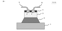
- FIG. 1 shows a joint portion of a semiconductor power module 100 according to the present invention.
- the substrate 1 is a DBC (Direct Bonded Copper) substrate or the like.
- the substrate 1 and the power semiconductor element 3 are joined by the Zn-based lead-free solder 2 according to the present application.
- Bonding pads (or electrodes) 6 are formed on the surface of the power semiconductor element 3.
- a resin film 4 having appropriate insulation and high heat resistance is formed around the bonding pad 6.
- a bonding wire 5 is connected to the bonding pad 6.
- the Zn-based lead-free solder according to the present application can also be used for joining lead terminals.
- the resin film 4 is made of a polyimide resin, a phenol resin, a polybenzoxazole (PBO) resin, a silicone resin, or the like.
- the polyimide film has a very high heat resistance with a decomposition temperature of 500 ° C. or higher, but the adhesion between the polyimide film and the power semiconductor element 3 is not so high. When the operating temperature of the semiconductor power module 100 reaches 350 ° C. or higher, the polyimide film is peeled off.
- the power semiconductor element 3 in addition to silicon (Si), those formed of a wide band gap semiconductor having a band gap larger than that of silicon can be suitably used.
- the wide band gap semiconductor include silicon carbide (SiC), a gallium nitride material, and diamond.
- Fig. 2 shows the characteristics of elements having eutectic points with Zn. Since the melting point of zinc itself is 420 ° C., an appropriate amount of an element having a eutectic point with Zn or a low melting point element is added to produce a Zn-based lead-free solder. Among them, the most effective additive element for setting the melting point to 300 to 350 ° C. is Mg having a eutectic point of 364 ° C. at 3 wt%. However, when Mg is added, the solder becomes hard and brittle, and easily oxidized. Even when the addition amount is substantially 0.1 wt%, the initial bondability and heat cycleability of the solder are greatly reduced. Therefore, Mg is very effective for lowering the melting point, but is not added substantially.
- Al As another element that lowers the melting point of Zn-based solder, Al has a eutectic point of 6 wt%. Although Al is not as much as Mg, it is a material that is easier to oxidize than Zn. Therefore, when Al is added, the initial bondability of the solder decreases. However, since Al is a relatively soft material, solder exhibits satisfactory heat cycle properties. Therefore, the addition amount of Al is suppressed to such an extent that the initial bondability is not deteriorated. In Patent Document 1, 1 to 10 wt% of Al is added. Since the initial bondability is greatly lowered at such an addition amount, the addition amount of Al is substantially less than 1 wt%.
- Patent Document 2 Al is added in an amount of 3.0 to 7.0 wt%, and Mg is added in an amount of 0.3 to 4.0 wt%. With such an added amount, the initial bondability and heat cycleability are greatly reduced, so the added amount of Al is substantially less than 1 wt%. Since it is desirable not to add Mg, in Embodiment 2 of the present invention, Mg is not added to Zn. The aim is to keep the melting point of Zn-based solder containing Zn as the main component within the range of 300 to 350 ° C. by suppressing the amount of Al added and adjusting other additive elements. Furthermore, the solder composition is optimized using heat cycle properties and initial bondability as indices.
- Zn, Al, Ge, Mn, Sb, and Cr having a purity of 99.9% by mass or more were prepared as raw materials. Large flakes and bulk-shaped raw materials were reduced to a size of 3 mm or less by cutting and crushing while paying attention to ensure that the alloy after melting did not vary in composition depending on the sampling location. Next, a predetermined amount of these raw materials was weighed and put into a graphite crucible for a high-frequency melting furnace.
- the crucible containing each raw material was placed in a high-frequency melting furnace and heated and melted in the apparatus in a nitrogen atmosphere to suppress oxidation (nitrogen flow rate: 0.5 l / min).
- nitrogen flow rate 0.5 l / min.
- the metal began to melt, it was stirred well with a mixing rod and mixed uniformly so as not to cause local compositional variations.
- the high frequency power supply was turned off, the crucible was quickly taken out, and the molten metal in the crucible was poured into the mold of the solder mother alloy.
- a mold having the same shape as that generally used in the production of a solder mother alloy was used.
- a solidus temperature was measured as a substantial melting point of each solder using a differential scanning calorimetry (DSC). .
- the melting point analysis was performed by applying heat twice to confirm whether the sample was first heated and then melted even if heated.
- the measurement temperature profile was raised to 400 ° C. by raising the temperature at 10 ° C./min with 15 ° C. as the measurement start point. Then, it cooled at 5 degrees C / min. If the scanning is performed only once, a peak different from the fact may occur due to the influence of impurities and surface deposits remaining inside. It is preferable to perform the process twice in this manner because the temperature is in accordance with the actual profile.
- This measurement also includes an evaluation of whether or not it is remelted after being joined once.
- each solder mother alloy was rolled to produce a molded solder having a thickness of 0.3 mm (size: 20 mm ⁇ 20 mm).
- a DBC (Direct Bonded Copper) substrate having a thickness of 1.2 mm and a SiC element having a thickness of 0.25 mm were joined in a hydrogen reduction atmosphere at a sample temperature of 350 ° C. (10 min).
- the DBC substrate corresponds to the substrate 1 in FIG. 1
- the SiC element corresponds to the power semiconductor element 3 in FIG.
- the SiC element (thermal expansion coefficient ⁇ : 4 ppm; size: 20 mm ⁇ 20 mm) has Au metallized on the outermost surface.
- Five samples were prepared for each composition. After joining, the void ratio (white portion) was calculated by observing an ultrasonic flaw detector (SAT: Scanning Acoustic Tomograph). When all the void ratios were 20% or less, the initial bondability was evaluated as “ ⁇ ”, and when one void was higher than 20%, the initial bondability was evaluated as “X”.
- the crack portion is also white, so the white portion (initial void + crack) calculated from the SAT image after the heat cycle is calculated from the ratio of the white portion (initial void) calculated from the SAT image observed in the initial bonded state. ) To calculate the degree of crack propagation.
- the heat cycle property column in the figure was marked with ⁇ , and when greater than 50%, it was marked with ⁇ .
- the thermal conductivity of Zn is about 120 W / m ⁇ K
- Sn-3Ag-0.5Cu solder, which has been used for general purposes is about 60 W / m ⁇ K
- Pb-5Sn solder is 35 W / m ⁇ K. It is.
- the reason for setting the heat cycle threshold to 50% this time is that it is judged that it is possible to take advantage of the superior thermal conductivity of Zn-based solder if the crack does not progress approximately at the joint. .
- the overall evaluation is ⁇ , if all satisfy a certain standard, the overall evaluation is ⁇ It was described in the column of comprehensive evaluation in the figure. In Examples 1 to 32, the overall evaluation is good. In Comparative Examples 1 to 16, the overall evaluation is x. As a result, the main component Zn contains 1.0 to 5.8 wt% Ge, 0.05 to 0.2 wt% Cr, 0.25 to 1.0 wt% Al, and 5 to 10 wt Ga. %, And 0.5 to 2.0 wt% Sb, good results were obtained. Next, the reasons why the above amounts are specified for the respective compositions are shown below.
- Al (0.25 to 1.0 wt%) Reason The eutectic point with Zn is 6 wt%. Since Al is easily oxidized, it is necessary to reduce it as much as possible. If the amount of Al added is about 1 wt%, oxidation is suppressed and the eutectic is approached, so the melting point is lowered. When Al is less than 0.25 wt%, the melting point lowering effect cannot be obtained, and it can be easily estimated from the result of the melting point measurement of each composition in the figure that the temperature exceeds 350 ° C.
- the addition amount of Al is preferably 0.25 to 1.0 wt%.
- Ge (1.0-5.8wt%) Reason Since the eutectic point with Zn is 5.8 wt%, if it is less than 1 wt%, the melting point lowering effect is small, and it can be easily estimated from the result of the melting point measurement of each composition in the figure that it exceeds 350 ° C. On the other hand, when Ge is larger than 5.8 wt%, the melting point becomes higher than the eutectic point, so that the melting point becomes high. Further, since extremely coarse precipitates increase, it becomes hard and brittle, the deterioration in heat cycle is remarkably accelerated, and the crack progress exceeds 50% (Comparative Examples 3 to 6). Therefore, the addition amount of Ge is preferably 1.0 to 5.8 wt%.
- Ga (5-10wt%) Reason Since Ga itself has a low melting point, the addition of 5 wt% or more lowers the melting point appropriately. When Ga is less than 5 wt%, the melting point lowering effect is not obtained, and it can be easily estimated from the result of the melting point measurement of each composition in the figure that the temperature exceeds 350 ° C. On the other hand, when Ga is larger than 10 wt% (Comparative Example 7 and Comparative Example 8), the melting point becomes lower than 300 ° C. due to excessive addition. In addition, a low melting point phase of Ga alone or Zn and a eutectic is not preferable because DSC measurement results show it. Therefore, the addition amount of Ga is preferably 5 to 10 wt%. Here, the additive amount of Ga indicates a value obtained by rounding off one decimal place.
- Sb (0.5-2.0wt%) Reason Since the eutectic point with Zn is 2 wt%, it is smaller than Al, Ge, and Ga, but has an effect of lowering the melting point by about 10 ° C. When Sb is smaller than 0.5 wt% (Comparative Example 9 and Comparative Example 10), the low melting point effect cannot be obtained. Further, the DSC result is not preferable because a low melting point phase of Ga alone and GaZn eutectic is observed. On the other hand, when Sb is larger than 2 wt% (Comparative Example 11 and Comparative Example 12), formation of a low melting point phase is suppressed, but excessively large precipitates increased due to excessive addition.
- the addition amount of Sb is preferably 0.5 to 2.0 wt%.
- the addition amount of Cr is preferably 0.05 to 0.2 wt%.
- Mn an additive element that exhibits the same effect as Sb is Mn.
- Mn an additive element that exhibits the same effect as Sb.
- In is an example of an additive element that exhibits the same effect as Ga. Specifically, when In is smaller than 10 wt%, the melting point lowering effect cannot be obtained, and the melting point exceeds 350 ° C. On the other hand, when In was larger than 20 wt%, the melting point became less than 300 ° C. due to excessive addition. Moreover, since the low melting point phase of In alone or InZn eutectic was seen from the DSC measurement result, it is not preferable. Therefore, the addition amount of In is preferably 10 to 20 wt%. In any case, the Zn-based lead-free solder according to the present application has a melting point of substantially 300 to 350 ° C. Here, the added amount of In indicates a value obtained by rounding off one decimal place.
- the Zn-based lead-free solder according to the present application is effective for lowering the melting point, it is easy to oxidize and does not contain Mg, which tends to become hard and brittle with a small amount of addition. Further, the addition of Cr refines the Zn structure and improves the heat cycle performance. Also, when Al is added, the melting point is lowered, but since it is easily oxidized, the initial joining property is satisfied by making the amount of Al added 1 wt% or less. Further, although the melting point is lowered by adding Ga, a low melting point phase partially formed of Ga alone or eutectic with Zn is formed. In order to suppress this, it becomes possible to add Sb or Mn, partially form an alloy phase with Ga, and suppress the formation of a low melting point phase due to Ga addition.
- the power semiconductor element When SiC is used for the power semiconductor element, the power semiconductor element is operated at a higher temperature than that of Si in order to take advantage of its characteristics. In semiconductor power semiconductors equipped with SiC devices, higher reliability is required as a power semiconductor element. Therefore, the merit of the present invention for realizing a highly reliable power semiconductor device is more effective. .
Abstract
Priority Applications (4)
| Application Number | Priority Date | Filing Date | Title |
|---|---|---|---|
| DE112013007179.7T DE112013007179T5 (de) | 2013-06-20 | 2013-12-13 | Zn-Basiertes bleifreies Lot und Halbleiterleistungsmodul |
| JP2015522470A JPWO2014203425A1 (ja) | 2013-06-20 | 2013-12-13 | Zn系鉛フリーはんだおよび半導体パワーモジュール |
| US14/890,202 US20160082552A1 (en) | 2013-06-20 | 2013-12-13 | Zn based lead-free solder and semiconductor power module |
| CN201380077495.1A CN105324209A (zh) | 2013-06-20 | 2013-12-13 | Zn系无铅焊料和半导体功率模块 |
Applications Claiming Priority (2)
| Application Number | Priority Date | Filing Date | Title |
|---|---|---|---|
| JP2013-129243 | 2013-06-20 | ||
| JP2013129243 | 2013-06-20 |
Publications (1)
| Publication Number | Publication Date |
|---|---|
| WO2014203425A1 true WO2014203425A1 (fr) | 2014-12-24 |
Family
ID=52104183
Family Applications (1)
| Application Number | Title | Priority Date | Filing Date |
|---|---|---|---|
| PCT/JP2013/083448 WO2014203425A1 (fr) | 2013-06-20 | 2013-12-13 | Brasure sans plomb à base de zn et module d'alimentation à semi-conducteurs |
Country Status (5)
| Country | Link |
|---|---|
| US (1) | US20160082552A1 (fr) |
| JP (1) | JPWO2014203425A1 (fr) |
| CN (1) | CN105324209A (fr) |
| DE (1) | DE112013007179T5 (fr) |
| WO (1) | WO2014203425A1 (fr) |
Families Citing this family (8)
| Publication number | Priority date | Publication date | Assignee | Title |
|---|---|---|---|---|
| JPWO2014142153A1 (ja) * | 2013-03-13 | 2017-02-16 | 株式会社日本スペリア社 | はんだ接合物及びはんだ接合方法 |
| TWI561639B (en) * | 2014-04-17 | 2016-12-11 | Heraeus Materials Singapore Pte Ltd | Lead-free eutectic solder alloy comprising zinc as the main component and aluminum as an alloying metal |
| CN107052614A (zh) * | 2016-11-30 | 2017-08-18 | 安徽华众焊业有限公司 | 无银黄铜焊料 |
| CN106695164A (zh) * | 2016-11-30 | 2017-05-24 | 安徽华众焊业有限公司 | 黄铜焊料 |
| CN106624443A (zh) * | 2016-11-30 | 2017-05-10 | 安徽华众焊业有限公司 | 黄铜钎料合金 |
| CN106736010A (zh) * | 2016-11-30 | 2017-05-31 | 安徽华众焊业有限公司 | 铜锌钎焊膏 |
| CN106514050A (zh) * | 2016-12-29 | 2017-03-22 | 安徽华众焊业有限公司 | 一种黄铜钎料及其制备方法 |
| CN111676390B (zh) * | 2020-08-03 | 2022-03-11 | 北京科技大学 | 一种Zn-Ga系合金及其制备方法与应用 |
Citations (5)
| Publication number | Priority date | Publication date | Assignee | Title |
|---|---|---|---|---|
| JPH0796389A (ja) * | 1993-09-29 | 1995-04-11 | Furukawa Electric Co Ltd:The | アルミ製熱交換器用複合チューブとその製造方法 |
| JPH11172353A (ja) * | 1997-12-04 | 1999-06-29 | Sumitomo Metal Mining Co Ltd | 高温はんだ付用Zn合金 |
| JPH11288955A (ja) * | 1998-04-02 | 1999-10-19 | Sumitomo Metal Mining Co Ltd | 高温はんだ付用Zn合金 |
| JP2006255762A (ja) * | 2005-03-18 | 2006-09-28 | Uchihashi Estec Co Ltd | 電子部品用線状はんだ |
| JP2012183558A (ja) * | 2011-03-07 | 2012-09-27 | Nihon Superior Co Ltd | 鉛フリーはんだ合金及びそれを用いたはんだ継手 |
Family Cites Families (8)
| Publication number | Priority date | Publication date | Assignee | Title |
|---|---|---|---|---|
| JPS53124150A (en) * | 1977-04-05 | 1978-10-30 | Nec Corp | Alloy soldering material |
| US20030007885A1 (en) * | 1999-03-16 | 2003-01-09 | Shinjiro Domi | Lead-free solder |
| TWI248384B (en) * | 2000-06-12 | 2006-02-01 | Hitachi Ltd | Electronic device |
| JP3800977B2 (ja) * | 2001-04-11 | 2006-07-26 | 株式会社日立製作所 | Zn−Al系はんだを用いた製品 |
| JPWO2003021664A1 (ja) * | 2001-08-31 | 2005-07-07 | 株式会社日立製作所 | 半導体装置、構造体及び電子装置 |
| CN100352595C (zh) * | 2005-08-04 | 2007-12-05 | 上海交通大学 | Sn-Zn-Bi-Cr合金无铅焊料 |
| CN100513640C (zh) * | 2007-05-17 | 2009-07-15 | 戴国水 | 一种无铅喷金料 |
| US9735126B2 (en) * | 2011-06-07 | 2017-08-15 | Infineon Technologies Ag | Solder alloys and arrangements |
-
2013
- 2013-12-13 DE DE112013007179.7T patent/DE112013007179T5/de not_active Withdrawn
- 2013-12-13 WO PCT/JP2013/083448 patent/WO2014203425A1/fr active Application Filing
- 2013-12-13 US US14/890,202 patent/US20160082552A1/en not_active Abandoned
- 2013-12-13 JP JP2015522470A patent/JPWO2014203425A1/ja active Pending
- 2013-12-13 CN CN201380077495.1A patent/CN105324209A/zh active Pending
Patent Citations (5)
| Publication number | Priority date | Publication date | Assignee | Title |
|---|---|---|---|---|
| JPH0796389A (ja) * | 1993-09-29 | 1995-04-11 | Furukawa Electric Co Ltd:The | アルミ製熱交換器用複合チューブとその製造方法 |
| JPH11172353A (ja) * | 1997-12-04 | 1999-06-29 | Sumitomo Metal Mining Co Ltd | 高温はんだ付用Zn合金 |
| JPH11288955A (ja) * | 1998-04-02 | 1999-10-19 | Sumitomo Metal Mining Co Ltd | 高温はんだ付用Zn合金 |
| JP2006255762A (ja) * | 2005-03-18 | 2006-09-28 | Uchihashi Estec Co Ltd | 電子部品用線状はんだ |
| JP2012183558A (ja) * | 2011-03-07 | 2012-09-27 | Nihon Superior Co Ltd | 鉛フリーはんだ合金及びそれを用いたはんだ継手 |
Also Published As
| Publication number | Publication date |
|---|---|
| JPWO2014203425A1 (ja) | 2017-02-23 |
| US20160082552A1 (en) | 2016-03-24 |
| DE112013007179T5 (de) | 2016-04-28 |
| CN105324209A (zh) | 2016-02-10 |
Similar Documents
| Publication | Publication Date | Title |
|---|---|---|
| WO2014203425A1 (fr) | Brasure sans plomb à base de zn et module d'alimentation à semi-conducteurs | |
| JP5585746B2 (ja) | 高温鉛フリーはんだ合金 | |
| KR101285958B1 (ko) | 땜납 합금 및 반도체 장치 | |
| JP4453612B2 (ja) | 無鉛はんだ合金 | |
| JP6516013B2 (ja) | 半導体装置用はんだ材 | |
| JP5614507B2 (ja) | Sn−Cu系鉛フリーはんだ合金 | |
| JP5206779B2 (ja) | Znを主成分とするPbフリーはんだ合金 | |
| JP5861559B2 (ja) | PbフリーIn系はんだ合金 | |
| JP6751250B1 (ja) | はんだ合金、はんだペースト、はんだプリフォーム及びはんだ継手 | |
| TWI469845B (zh) | High temperature lead free solder alloy | |
| WO2018168858A1 (fr) | Matériau de soudage | |
| JP6136878B2 (ja) | Bi基はんだ合金とその製造方法、並びにそれを用いた電子部品のボンディング方法および電子部品実装基板 | |
| JP5958811B2 (ja) | はんだ材料及びこれを用いた実装構造体 | |
| JP2005052869A (ja) | 高温はんだ付用ろう材とそれを用いた半導体装置 | |
| JP2011251329A (ja) | 高温鉛フリーはんだペースト | |
| JP2013081995A (ja) | Znを主成分とするPbフリーはんだ合金 | |
| JP2016093831A (ja) | Pbを含まないMg−Cu系はんだ合金 | |
| JP5861526B2 (ja) | Pbを含まないGe−Al系はんだ合金 | |
| JP2016097444A (ja) | Pbを含まないSb−In系はんだ合金 | |
| JP2014136236A (ja) | PbフリーIn系はんだ合金 | |
| JP2017136627A (ja) | PbフリーIn系はんだ合金 | |
| JP2018149554A (ja) | PbフリーBi系はんだ合金、該はんだ合金を用いた電子部品、および電子部品実装基板 | |
| JP2017029996A (ja) | Pbを含まないAg−Sb系はんだ合金 | |
| JP2015098048A (ja) | Pbを含まないZn−Ge系はんだ合金およびそれを用いた電子部品 | |
| JP2000351093A (ja) | 半田材料及びそれを用いた電子部品 |
Legal Events
| Date | Code | Title | Description |
|---|---|---|---|
| WWE | Wipo information: entry into national phase |
Ref document number: 201380077495.1 Country of ref document: CN |
|
| 121 | Ep: the epo has been informed by wipo that ep was designated in this application |
Ref document number: 13887367 Country of ref document: EP Kind code of ref document: A1 |
|
| ENP | Entry into the national phase |
Ref document number: 2015522470 Country of ref document: JP Kind code of ref document: A |
|
| WWE | Wipo information: entry into national phase |
Ref document number: 14890202 Country of ref document: US |
|
| WWE | Wipo information: entry into national phase |
Ref document number: 112013007179 Country of ref document: DE |
|
| 122 | Ep: pct application non-entry in european phase |
Ref document number: 13887367 Country of ref document: EP Kind code of ref document: A1 |