WO2014193033A1 - 화합물, 이를 포함하는 유기발광소자 및 상기 유기발광소자를 포함하는 표시장치 - Google Patents
화합물, 이를 포함하는 유기발광소자 및 상기 유기발광소자를 포함하는 표시장치 Download PDFInfo
- Publication number
- WO2014193033A1 WO2014193033A1 PCT/KR2013/007135 KR2013007135W WO2014193033A1 WO 2014193033 A1 WO2014193033 A1 WO 2014193033A1 KR 2013007135 W KR2013007135 W KR 2013007135W WO 2014193033 A1 WO2014193033 A1 WO 2014193033A1
- Authority
- WO
- WIPO (PCT)
- Prior art keywords
- substituted
- unsubstituted
- group
- formula
- independently
- Prior art date
Links
- 150000001875 compounds Chemical class 0.000 title claims abstract description 130
- 230000005525 hole transport Effects 0.000 claims description 36
- 125000000217 alkyl group Chemical group 0.000 claims description 32
- 125000003118 aryl group Chemical group 0.000 claims description 32
- 125000003983 fluorenyl group Chemical group C1(=CC=CC=2C3=CC=CC=C3CC12)* 0.000 claims description 27
- 239000010409 thin film Substances 0.000 claims description 27
- 229910052739 hydrogen Inorganic materials 0.000 claims description 26
- 239000001257 hydrogen Substances 0.000 claims description 26
- 238000002347 injection Methods 0.000 claims description 25
- 239000007924 injection Substances 0.000 claims description 25
- 150000002431 hydrogen Chemical class 0.000 claims description 24
- 238000000034 method Methods 0.000 claims description 24
- 239000000126 substance Substances 0.000 claims description 23
- 125000001072 heteroaryl group Chemical group 0.000 claims description 22
- -1 R 21 Chemical compound 0.000 claims description 20
- YZCKVEUIGOORGS-OUBTZVSYSA-N Deuterium Chemical compound [2H] YZCKVEUIGOORGS-OUBTZVSYSA-N 0.000 claims description 19
- 125000000732 arylene group Chemical group 0.000 claims description 19
- 229910052805 deuterium Inorganic materials 0.000 claims description 19
- 125000005567 fluorenylene group Chemical group 0.000 claims description 19
- 230000033228 biological regulation Effects 0.000 claims description 16
- 125000005549 heteroarylene group Chemical group 0.000 claims description 15
- 238000012937 correction Methods 0.000 claims description 14
- 125000000753 cycloalkyl group Chemical group 0.000 claims description 13
- 125000003808 silyl group Chemical group [H][Si]([H])([H])[*] 0.000 claims description 13
- 229910052799 carbon Inorganic materials 0.000 claims description 10
- OKTJSMMVPCPJKN-UHFFFAOYSA-N Carbon Chemical compound [C] OKTJSMMVPCPJKN-UHFFFAOYSA-N 0.000 claims description 6
- 125000004429 atom Chemical group 0.000 claims description 4
- UFHFLCQGNIYNRP-UHFFFAOYSA-N Hydrogen Chemical compound [H][H] UFHFLCQGNIYNRP-UHFFFAOYSA-N 0.000 claims description 3
- 125000004432 carbon atom Chemical group C* 0.000 claims description 3
- 229910052760 oxygen Inorganic materials 0.000 claims description 3
- 229910052717 sulfur Inorganic materials 0.000 claims description 3
- 230000005693 optoelectronics Effects 0.000 abstract description 13
- 239000010410 layer Substances 0.000 description 111
- YXFVVABEGXRONW-UHFFFAOYSA-N Toluene Chemical compound CC1=CC=CC=C1 YXFVVABEGXRONW-UHFFFAOYSA-N 0.000 description 108
- YMWUJEATGCHHMB-UHFFFAOYSA-N Dichloromethane Chemical compound ClCCl YMWUJEATGCHHMB-UHFFFAOYSA-N 0.000 description 93
- 239000000543 intermediate Substances 0.000 description 68
- CSNNHWWHGAXBCP-UHFFFAOYSA-L Magnesium sulfate Chemical compound [Mg+2].[O-][S+2]([O-])([O-])[O-] CSNNHWWHGAXBCP-UHFFFAOYSA-L 0.000 description 62
- XEKOWRVHYACXOJ-UHFFFAOYSA-N Ethyl acetate Chemical compound CCOC(C)=O XEKOWRVHYACXOJ-UHFFFAOYSA-N 0.000 description 60
- 230000015572 biosynthetic process Effects 0.000 description 58
- 238000003786 synthesis reaction Methods 0.000 description 58
- MFRIHAYPQRLWNB-UHFFFAOYSA-N sodium tert-butoxide Chemical compound [Na+].CC(C)(C)[O-] MFRIHAYPQRLWNB-UHFFFAOYSA-N 0.000 description 44
- 239000000463 material Substances 0.000 description 41
- 238000006243 chemical reaction Methods 0.000 description 40
- XLYOFNOQVPJJNP-UHFFFAOYSA-N water Chemical compound O XLYOFNOQVPJJNP-UHFFFAOYSA-N 0.000 description 32
- 239000012153 distilled water Substances 0.000 description 31
- 239000000706 filtrate Substances 0.000 description 31
- 229910052943 magnesium sulfate Inorganic materials 0.000 description 31
- 235000019341 magnesium sulphate Nutrition 0.000 description 31
- 238000010992 reflux Methods 0.000 description 31
- 239000012299 nitrogen atmosphere Substances 0.000 description 30
- 239000000047 product Substances 0.000 description 30
- 239000007787 solid Substances 0.000 description 29
- 239000012044 organic layer Substances 0.000 description 28
- 239000000203 mixture Substances 0.000 description 26
- 238000010898 silica gel chromatography Methods 0.000 description 24
- 238000003756 stirring Methods 0.000 description 22
- 230000000052 comparative effect Effects 0.000 description 14
- ILEFZGNFDZBUEC-UHFFFAOYSA-N C(CCC)C(CCCP)(CCCC)CCCC Chemical compound C(CCC)C(CCCP)(CCCC)CCCC ILEFZGNFDZBUEC-UHFFFAOYSA-N 0.000 description 12
- BWHDROKFUHTORW-UHFFFAOYSA-N tritert-butylphosphane Chemical compound CC(C)(C)P(C(C)(C)C)C(C)(C)C BWHDROKFUHTORW-UHFFFAOYSA-N 0.000 description 11
- BWHMMNNQKKPAPP-UHFFFAOYSA-L potassium carbonate Chemical compound [K+].[K+].[O-]C([O-])=O BWHMMNNQKKPAPP-UHFFFAOYSA-L 0.000 description 10
- 125000001424 substituent group Chemical group 0.000 description 10
- DMVOXQPQNTYEKQ-UHFFFAOYSA-N biphenyl-4-amine Chemical group C1=CC(N)=CC=C1C1=CC=CC=C1 DMVOXQPQNTYEKQ-UHFFFAOYSA-N 0.000 description 8
- 238000000605 extraction Methods 0.000 description 8
- 238000000746 purification Methods 0.000 description 8
- VYPSYNLAJGMNEJ-UHFFFAOYSA-N Silicium dioxide Chemical compound O=[Si]=O VYPSYNLAJGMNEJ-UHFFFAOYSA-N 0.000 description 7
- 238000004587 chromatography analysis Methods 0.000 description 7
- 239000011368 organic material Substances 0.000 description 7
- 239000000741 silica gel Substances 0.000 description 7
- 229910002027 silica gel Inorganic materials 0.000 description 7
- 239000000758 substrate Substances 0.000 description 7
- 238000001771 vacuum deposition Methods 0.000 description 7
- VQGHOUODWALEFC-UHFFFAOYSA-N 2-phenylpyridine Chemical compound C1=CC=CC=C1C1=CC=CC=N1 VQGHOUODWALEFC-UHFFFAOYSA-N 0.000 description 6
- UJOBWOGCFQCDNV-UHFFFAOYSA-N 9H-carbazole Chemical compound C1=CC=C2C3=CC=CC=C3NC2=C1 UJOBWOGCFQCDNV-UHFFFAOYSA-N 0.000 description 6
- KFZMGEQAYNKOFK-UHFFFAOYSA-N Isopropanol Chemical compound CC(C)O KFZMGEQAYNKOFK-UHFFFAOYSA-N 0.000 description 6
- 125000003277 amino group Chemical group 0.000 description 6
- 230000008859 change Effects 0.000 description 6
- 238000005259 measurement Methods 0.000 description 6
- FNKCOUREFBNNHG-UHFFFAOYSA-N 1,3-dibromo-5-chlorobenzene Chemical compound ClC1=CC(Br)=CC(Br)=C1 FNKCOUREFBNNHG-UHFFFAOYSA-N 0.000 description 5
- SPDPTFAJSFKAMT-UHFFFAOYSA-N 1-n-[4-[4-(n-[4-(3-methyl-n-(3-methylphenyl)anilino)phenyl]anilino)phenyl]phenyl]-4-n,4-n-bis(3-methylphenyl)-1-n-phenylbenzene-1,4-diamine Chemical group CC1=CC=CC(N(C=2C=CC(=CC=2)N(C=2C=CC=CC=2)C=2C=CC(=CC=2)C=2C=CC(=CC=2)N(C=2C=CC=CC=2)C=2C=CC(=CC=2)N(C=2C=C(C)C=CC=2)C=2C=C(C)C=CC=2)C=2C=C(C)C=CC=2)=C1 SPDPTFAJSFKAMT-UHFFFAOYSA-N 0.000 description 5
- CSCPPACGZOOCGX-UHFFFAOYSA-N Acetone Chemical compound CC(C)=O CSCPPACGZOOCGX-UHFFFAOYSA-N 0.000 description 5
- 238000011161 development Methods 0.000 description 5
- 230000018109 developmental process Effects 0.000 description 5
- 230000006870 function Effects 0.000 description 5
- 229910000027 potassium carbonate Inorganic materials 0.000 description 5
- RUFPHBVGCFYCNW-UHFFFAOYSA-N 1-naphthylamine Chemical compound C1=CC=C2C(N)=CC=CC2=C1 RUFPHBVGCFYCNW-UHFFFAOYSA-N 0.000 description 4
- DGAQECJNVWCQMB-PUAWFVPOSA-M Ilexoside XXIX Chemical compound C[C@@H]1CC[C@@]2(CC[C@@]3(C(=CC[C@H]4[C@]3(CC[C@@H]5[C@@]4(CC[C@@H](C5(C)C)OS(=O)(=O)[O-])C)C)[C@@H]2[C@]1(C)O)C)C(=O)O[C@H]6[C@@H]([C@H]([C@@H]([C@H](O6)CO)O)O)O.[Na+] DGAQECJNVWCQMB-PUAWFVPOSA-M 0.000 description 4
- XYFCBTPGUUZFHI-UHFFFAOYSA-N Phosphine Chemical compound P XYFCBTPGUUZFHI-UHFFFAOYSA-N 0.000 description 4
- WYURNTSHIVDZCO-UHFFFAOYSA-N Tetrahydrofuran Chemical compound C1CCOC1 WYURNTSHIVDZCO-UHFFFAOYSA-N 0.000 description 4
- XLOMVQKBTHCTTD-UHFFFAOYSA-N Zinc monoxide Chemical compound [Zn]=O XLOMVQKBTHCTTD-UHFFFAOYSA-N 0.000 description 4
- CUJRVFIICFDLGR-UHFFFAOYSA-N acetylacetonate Chemical compound CC(=O)[CH-]C(C)=O CUJRVFIICFDLGR-UHFFFAOYSA-N 0.000 description 4
- 239000007864 aqueous solution Substances 0.000 description 4
- 230000000903 blocking effect Effects 0.000 description 4
- ZUOUZKKEUPVFJK-UHFFFAOYSA-N diphenyl Chemical compound C1=CC=CC=C1C1=CC=CC=C1 ZUOUZKKEUPVFJK-UHFFFAOYSA-N 0.000 description 4
- 239000000284 extract Substances 0.000 description 4
- 108700039708 galantide Proteins 0.000 description 4
- 125000005842 heteroatom Chemical group 0.000 description 4
- 229910052751 metal Inorganic materials 0.000 description 4
- 239000002184 metal Substances 0.000 description 4
- 229910052757 nitrogen Inorganic materials 0.000 description 4
- 229910052708 sodium Inorganic materials 0.000 description 4
- 239000011734 sodium Substances 0.000 description 4
- TZMSYXZUNZXBOL-UHFFFAOYSA-N 10H-phenoxazine Chemical compound C1=CC=C2NC3=CC=CC=C3OC2=C1 TZMSYXZUNZXBOL-UHFFFAOYSA-N 0.000 description 3
- 238000005160 1H NMR spectroscopy Methods 0.000 description 3
- OKKJLVBELUTLKV-UHFFFAOYSA-N Methanol Chemical compound OC OKKJLVBELUTLKV-UHFFFAOYSA-N 0.000 description 3
- KWYUFKZDYYNOTN-UHFFFAOYSA-M Potassium hydroxide Chemical compound [OH-].[K+] KWYUFKZDYYNOTN-UHFFFAOYSA-M 0.000 description 3
- 125000005103 alkyl silyl group Chemical group 0.000 description 3
- 229910052782 aluminium Inorganic materials 0.000 description 3
- XAGFODPZIPBFFR-UHFFFAOYSA-N aluminium Chemical compound [Al] XAGFODPZIPBFFR-UHFFFAOYSA-N 0.000 description 3
- 239000011575 calcium Substances 0.000 description 3
- 150000001721 carbon Chemical group 0.000 description 3
- 125000004093 cyano group Chemical group *C#N 0.000 description 3
- 230000007423 decrease Effects 0.000 description 3
- 230000005283 ground state Effects 0.000 description 3
- 125000005843 halogen group Chemical group 0.000 description 3
- 125000002887 hydroxy group Chemical group [H]O* 0.000 description 3
- AMGQUBHHOARCQH-UHFFFAOYSA-N indium;oxotin Chemical compound [In].[Sn]=O AMGQUBHHOARCQH-UHFFFAOYSA-N 0.000 description 3
- 238000004519 manufacturing process Methods 0.000 description 3
- 125000001624 naphthyl group Chemical group 0.000 description 3
- 125000000449 nitro group Chemical group [O-][N+](*)=O 0.000 description 3
- 230000007704 transition Effects 0.000 description 3
- 125000002023 trifluoromethyl group Chemical group FC(F)(F)* 0.000 description 3
- MBMQEIFVQACCCH-QBODLPLBSA-N zearalenone Chemical compound O=C1O[C@@H](C)CCCC(=O)CCC\C=C\C2=CC(O)=CC(O)=C21 MBMQEIFVQACCCH-QBODLPLBSA-N 0.000 description 3
- CAYQIZIAYYNFCS-UHFFFAOYSA-N (4-chlorophenyl)boronic acid Chemical compound OB(O)C1=CC=C(Cl)C=C1 CAYQIZIAYYNFCS-UHFFFAOYSA-N 0.000 description 2
- YJTKZCDBKVTVBY-UHFFFAOYSA-N 1,3-Diphenylbenzene Chemical group C1=CC=CC=C1C1=CC=CC(C=2C=CC=CC=2)=C1 YJTKZCDBKVTVBY-UHFFFAOYSA-N 0.000 description 2
- DZHFFMWJXJBBRG-UHFFFAOYSA-N 1-bromo-3,5-dichlorobenzene Chemical compound ClC1=CC(Cl)=CC(Br)=C1 DZHFFMWJXJBBRG-UHFFFAOYSA-N 0.000 description 2
- FSEXLNMNADBYJU-UHFFFAOYSA-N 2-phenylquinoline Chemical compound C1=CC=CC=C1C1=CC=C(C=CC=C2)C2=N1 FSEXLNMNADBYJU-UHFFFAOYSA-N 0.000 description 2
- QENGPZGAWFQWCZ-UHFFFAOYSA-N 3-Methylthiophene Chemical compound CC=1C=CSC=1 QENGPZGAWFQWCZ-UHFFFAOYSA-N 0.000 description 2
- DLFVBJFMPXGRIB-UHFFFAOYSA-N Acetamide Chemical compound CC(N)=O DLFVBJFMPXGRIB-UHFFFAOYSA-N 0.000 description 2
- WFDIJRYMOXRFFG-UHFFFAOYSA-N Acetic anhydride Chemical compound CC(=O)OC(C)=O WFDIJRYMOXRFFG-UHFFFAOYSA-N 0.000 description 2
- LFQSCWFLJHTTHZ-UHFFFAOYSA-N Ethanol Chemical compound CCO LFQSCWFLJHTTHZ-UHFFFAOYSA-N 0.000 description 2
- PXHVJJICTQNCMI-UHFFFAOYSA-N Nickel Chemical compound [Ni] PXHVJJICTQNCMI-UHFFFAOYSA-N 0.000 description 2
- YTPLMLYBLZKORZ-UHFFFAOYSA-N Thiophene Chemical compound C=1C=CSC=1 YTPLMLYBLZKORZ-UHFFFAOYSA-N 0.000 description 2
- 239000007983 Tris buffer Substances 0.000 description 2
- 238000013019 agitation Methods 0.000 description 2
- 239000000956 alloy Substances 0.000 description 2
- 229910045601 alloy Inorganic materials 0.000 description 2
- 238000004458 analytical method Methods 0.000 description 2
- QVGXLLKOCUKJST-UHFFFAOYSA-N atomic oxygen Chemical compound [O] QVGXLLKOCUKJST-UHFFFAOYSA-N 0.000 description 2
- 230000008901 benefit Effects 0.000 description 2
- 235000010290 biphenyl Nutrition 0.000 description 2
- 239000004305 biphenyl Substances 0.000 description 2
- 125000000609 carbazolyl group Chemical group C1(=CC=CC=2C3=CC=CC=C3NC12)* 0.000 description 2
- 238000012512 characterization method Methods 0.000 description 2
- 239000011248 coating agent Substances 0.000 description 2
- 238000000576 coating method Methods 0.000 description 2
- DMBHHRLKUKUOEG-UHFFFAOYSA-N diphenylamine Chemical compound C=1C=CC=CC=1NC1=CC=CC=C1 DMBHHRLKUKUOEG-UHFFFAOYSA-N 0.000 description 2
- 239000002019 doping agent Substances 0.000 description 2
- 230000000694 effects Effects 0.000 description 2
- 125000001495 ethyl group Chemical group [H]C([H])([H])C([H])([H])* 0.000 description 2
- 239000010408 film Substances 0.000 description 2
- 239000011521 glass Substances 0.000 description 2
- 230000009477 glass transition Effects 0.000 description 2
- 238000004770 highest occupied molecular orbital Methods 0.000 description 2
- 125000000959 isobutyl group Chemical group [H]C([H])([H])C([H])(C([H])([H])[H])C([H])([H])* 0.000 description 2
- 125000001449 isopropyl group Chemical group [H]C([H])([H])C([H])(*)C([H])([H])[H] 0.000 description 2
- 230000033001 locomotion Effects 0.000 description 2
- 150000002739 metals Chemical class 0.000 description 2
- VNWKTOKETHGBQD-UHFFFAOYSA-N methane Chemical compound C VNWKTOKETHGBQD-UHFFFAOYSA-N 0.000 description 2
- 125000002496 methyl group Chemical group [H]C([H])([H])* 0.000 description 2
- YGNUPJXMDOFFDO-UHFFFAOYSA-N n,4-diphenylaniline Chemical compound C=1C=C(C=2C=CC=CC=2)C=CC=1NC1=CC=CC=C1 YGNUPJXMDOFFDO-UHFFFAOYSA-N 0.000 description 2
- 239000007773 negative electrode material Substances 0.000 description 2
- 239000001301 oxygen Substances 0.000 description 2
- NFHFRUOZVGFOOS-UHFFFAOYSA-N palladium;triphenylphosphane Chemical compound [Pd].C1=CC=CC=C1P(C=1C=CC=CC=1)C1=CC=CC=C1.C1=CC=CC=C1P(C=1C=CC=CC=1)C1=CC=CC=C1.C1=CC=CC=C1P(C=1C=CC=CC=1)C1=CC=CC=C1.C1=CC=CC=C1P(C=1C=CC=CC=1)C1=CC=CC=C1 NFHFRUOZVGFOOS-UHFFFAOYSA-N 0.000 description 2
- 125000001997 phenyl group Chemical group [H]C1=C([H])C([H])=C(*)C([H])=C1[H] 0.000 description 2
- 229910052698 phosphorus Inorganic materials 0.000 description 2
- 229910000073 phosphorus hydride Inorganic materials 0.000 description 2
- 238000005424 photoluminescence Methods 0.000 description 2
- BASFCYQUMIYNBI-UHFFFAOYSA-N platinum Chemical compound [Pt] BASFCYQUMIYNBI-UHFFFAOYSA-N 0.000 description 2
- 125000001436 propyl group Chemical group [H]C([*])([H])C([H])([H])C([H])([H])[H] 0.000 description 2
- 230000004044 response Effects 0.000 description 2
- 230000033764 rhythmic process Effects 0.000 description 2
- 239000000243 solution Substances 0.000 description 2
- 239000002904 solvent Substances 0.000 description 2
- 238000004528 spin coating Methods 0.000 description 2
- 238000012916 structural analysis Methods 0.000 description 2
- 125000000999 tert-butyl group Chemical group [H]C([H])([H])C(*)(C([H])([H])[H])C([H])([H])[H] 0.000 description 2
- XOLBLPGZBRYERU-UHFFFAOYSA-N tin dioxide Chemical compound O=[Sn]=O XOLBLPGZBRYERU-UHFFFAOYSA-N 0.000 description 2
- 125000004950 trifluoroalkyl group Chemical group 0.000 description 2
- 238000005406 washing Methods 0.000 description 2
- 239000011787 zinc oxide Substances 0.000 description 2
- NAWXUBYGYWOOIX-SFHVURJKSA-N (2s)-2-[[4-[2-(2,4-diaminoquinazolin-6-yl)ethyl]benzoyl]amino]-4-methylidenepentanedioic acid Chemical compound C1=CC2=NC(N)=NC(N)=C2C=C1CCC1=CC=C(C(=O)N[C@@H](CC(=C)C(O)=O)C(O)=O)C=C1 NAWXUBYGYWOOIX-SFHVURJKSA-N 0.000 description 1
- 125000000008 (C1-C10) alkyl group Chemical group 0.000 description 1
- 125000004169 (C1-C6) alkyl group Chemical group 0.000 description 1
- POILWHVDKZOXJZ-ARJAWSKDSA-M (z)-4-oxopent-2-en-2-olate Chemical compound C\C([O-])=C\C(C)=O POILWHVDKZOXJZ-ARJAWSKDSA-M 0.000 description 1
- UCCUXODGPMAHRL-UHFFFAOYSA-N 1-bromo-4-iodobenzene Chemical compound BrC1=CC=C(I)C=C1 UCCUXODGPMAHRL-UHFFFAOYSA-N 0.000 description 1
- RNEOFIVNTNLSEH-UHFFFAOYSA-N 2-bromo-1-benzofuran Chemical compound C1=CC=C2OC(Br)=CC2=C1 RNEOFIVNTNLSEH-UHFFFAOYSA-N 0.000 description 1
- CRJISNQTZDMKQD-UHFFFAOYSA-N 2-bromodibenzofuran Chemical compound C1=CC=C2C3=CC(Br)=CC=C3OC2=C1 CRJISNQTZDMKQD-UHFFFAOYSA-N 0.000 description 1
- IJICRIUYZZESMW-UHFFFAOYSA-N 2-bromodibenzothiophene Chemical compound C1=CC=C2C3=CC(Br)=CC=C3SC2=C1 IJICRIUYZZESMW-UHFFFAOYSA-N 0.000 description 1
- TWPMMLHBHPYSMT-UHFFFAOYSA-N 3-methyl-n-phenylaniline Chemical compound CC1=CC=CC(NC=2C=CC=CC=2)=C1 TWPMMLHBHPYSMT-UHFFFAOYSA-N 0.000 description 1
- 229910016036 BaF 2 Inorganic materials 0.000 description 1
- 0 C*=[C+][C@@](*)NCCCC=*=C(C)C Chemical compound C*=[C+][C@@](*)NCCCC=*=C(C)C 0.000 description 1
- OYPRJOBELJOOCE-UHFFFAOYSA-N Calcium Chemical compound [Ca] OYPRJOBELJOOCE-UHFFFAOYSA-N 0.000 description 1
- VYZAMTAEIAYCRO-UHFFFAOYSA-N Chromium Chemical compound [Cr] VYZAMTAEIAYCRO-UHFFFAOYSA-N 0.000 description 1
- 241000238586 Cirripedia Species 0.000 description 1
- RYGMFSIKBFXOCR-UHFFFAOYSA-N Copper Chemical compound [Cu] RYGMFSIKBFXOCR-UHFFFAOYSA-N 0.000 description 1
- 229910052688 Gadolinium Inorganic materials 0.000 description 1
- 241000238631 Hexapoda Species 0.000 description 1
- WHXSMMKQMYFTQS-UHFFFAOYSA-N Lithium Chemical compound [Li] WHXSMMKQMYFTQS-UHFFFAOYSA-N 0.000 description 1
- FYYHWMGAXLPEAU-UHFFFAOYSA-N Magnesium Chemical compound [Mg] FYYHWMGAXLPEAU-UHFFFAOYSA-N 0.000 description 1
- 238000005481 NMR spectroscopy Methods 0.000 description 1
- CTQNGGLPUBDAKN-UHFFFAOYSA-N O-Xylene Chemical compound CC1=CC=CC=C1C CTQNGGLPUBDAKN-UHFFFAOYSA-N 0.000 description 1
- 229920001609 Poly(3,4-ethylenedioxythiophene) Polymers 0.000 description 1
- ZLMJMSJWJFRBEC-UHFFFAOYSA-N Potassium Chemical compound [K] ZLMJMSJWJFRBEC-UHFFFAOYSA-N 0.000 description 1
- BQCADISMDOOEFD-UHFFFAOYSA-N Silver Chemical compound [Ag] BQCADISMDOOEFD-UHFFFAOYSA-N 0.000 description 1
- ATJFFYVFTNAWJD-UHFFFAOYSA-N Tin Chemical compound [Sn] ATJFFYVFTNAWJD-UHFFFAOYSA-N 0.000 description 1
- RTAQQCXQSZGOHL-UHFFFAOYSA-N Titanium Chemical compound [Ti] RTAQQCXQSZGOHL-UHFFFAOYSA-N 0.000 description 1
- YZCKVEUIGOORGS-NJFSPNSNSA-N Tritium Chemical compound [3H] YZCKVEUIGOORGS-NJFSPNSNSA-N 0.000 description 1
- 206010047571 Visual impairment Diseases 0.000 description 1
- HCHKCACWOHOZIP-UHFFFAOYSA-N Zinc Chemical compound [Zn] HCHKCACWOHOZIP-UHFFFAOYSA-N 0.000 description 1
- 125000000641 acridinyl group Chemical group C1(=CC=CC2=NC3=CC=CC=C3C=C12)* 0.000 description 1
- 125000001931 aliphatic group Chemical group 0.000 description 1
- 239000010405 anode material Substances 0.000 description 1
- 125000002178 anthracenyl group Chemical group C1(=CC=CC2=CC3=CC=CC=C3C=C12)* 0.000 description 1
- 125000004653 anthracenylene group Chemical group 0.000 description 1
- YCOXTKKNXUZSKD-UHFFFAOYSA-N as-o-xylenol Natural products CC1=CC=C(O)C=C1C YCOXTKKNXUZSKD-UHFFFAOYSA-N 0.000 description 1
- 229910052788 barium Inorganic materials 0.000 description 1
- DSAJWYNOEDNPEQ-UHFFFAOYSA-N barium atom Chemical compound [Ba] DSAJWYNOEDNPEQ-UHFFFAOYSA-N 0.000 description 1
- 230000004888 barrier function Effects 0.000 description 1
- 125000003785 benzimidazolyl group Chemical group N1=C(NC2=C1C=CC=C2)* 0.000 description 1
- 125000000499 benzofuranyl group Chemical group O1C(=CC2=C1C=CC=C2)* 0.000 description 1
- 125000004196 benzothienyl group Chemical group S1C(=CC2=C1C=CC=C2)* 0.000 description 1
- 125000004622 benzoxazinyl group Chemical group O1NC(=CC2=C1C=CC=C2)* 0.000 description 1
- 125000006267 biphenyl group Chemical group 0.000 description 1
- 125000002529 biphenylenyl group Chemical group C1(=CC=CC=2C3=CC=CC=C3C12)* 0.000 description 1
- 125000000484 butyl group Chemical group [H]C([*])([H])C([H])([H])C([H])([H])C([H])([H])[H] 0.000 description 1
- DLIJPAHLBJIQHE-UHFFFAOYSA-N butylphosphane Chemical compound CCCCP DLIJPAHLBJIQHE-UHFFFAOYSA-N 0.000 description 1
- 229910052792 caesium Inorganic materials 0.000 description 1
- TVFDJXOCXUVLDH-UHFFFAOYSA-N caesium atom Chemical compound [Cs] TVFDJXOCXUVLDH-UHFFFAOYSA-N 0.000 description 1
- 229910052791 calcium Inorganic materials 0.000 description 1
- 229910052804 chromium Inorganic materials 0.000 description 1
- 239000011651 chromium Substances 0.000 description 1
- 125000002676 chrysenyl group Chemical group C1(=CC=CC=2C3=CC=C4C=CC=CC4=C3C=CC12)* 0.000 description 1
- 239000012141 concentrate Substances 0.000 description 1
- 229920001940 conductive polymer Polymers 0.000 description 1
- 239000004020 conductor Substances 0.000 description 1
- 230000021615 conjugation Effects 0.000 description 1
- 239000000470 constituent Substances 0.000 description 1
- 229910052802 copper Inorganic materials 0.000 description 1
- 239000010949 copper Substances 0.000 description 1
- GBRBMTNGQBKBQE-UHFFFAOYSA-L copper;diiodide Chemical compound I[Cu]I GBRBMTNGQBKBQE-UHFFFAOYSA-L 0.000 description 1
- 125000001995 cyclobutyl group Chemical group [H]C1([H])C([H])([H])C([H])(*)C1([H])[H] 0.000 description 1
- 125000001511 cyclopentyl group Chemical group [H]C1([H])C([H])([H])C([H])([H])C([H])(*)C1([H])[H] 0.000 description 1
- 125000001559 cyclopropyl group Chemical group [H]C1([H])C([H])([H])C1([H])* 0.000 description 1
- ZXHUJRZYLRVVNP-UHFFFAOYSA-N dibenzofuran-4-ylboronic acid Chemical compound C12=CC=CC=C2OC2=C1C=CC=C2B(O)O ZXHUJRZYLRVVNP-UHFFFAOYSA-N 0.000 description 1
- GOXNHPQCCUVWRO-UHFFFAOYSA-N dibenzothiophen-4-ylboronic acid Chemical compound C12=CC=CC=C2SC2=C1C=CC=C2B(O)O GOXNHPQCCUVWRO-UHFFFAOYSA-N 0.000 description 1
- 125000005509 dibenzothiophenyl group Chemical group 0.000 description 1
- PTLIZOFGXLGHSY-UHFFFAOYSA-N dibutylphosphane Chemical compound CCCCPCCCC PTLIZOFGXLGHSY-UHFFFAOYSA-N 0.000 description 1
- YMWUJEATGCHHMB-DICFDUPASA-N dichloromethane-d2 Chemical compound [2H]C([2H])(Cl)Cl YMWUJEATGCHHMB-DICFDUPASA-N 0.000 description 1
- 238000007598 dipping method Methods 0.000 description 1
- 238000004090 dissolution Methods 0.000 description 1
- WSUTUEIGSOWBJO-UHFFFAOYSA-N dizinc oxygen(2-) Chemical compound [O-2].[O-2].[Zn+2].[Zn+2] WSUTUEIGSOWBJO-UHFFFAOYSA-N 0.000 description 1
- 238000005516 engineering process Methods 0.000 description 1
- 238000001704 evaporation Methods 0.000 description 1
- 230000008020 evaporation Effects 0.000 description 1
- 230000005281 excited state Effects 0.000 description 1
- 125000000524 functional group Chemical group 0.000 description 1
- 125000002541 furyl group Chemical group 0.000 description 1
- UIWYJDYFSGRHKR-UHFFFAOYSA-N gadolinium atom Chemical compound [Gd] UIWYJDYFSGRHKR-UHFFFAOYSA-N 0.000 description 1
- PCHJSUWPFVWCPO-UHFFFAOYSA-N gold Chemical compound [Au] PCHJSUWPFVWCPO-UHFFFAOYSA-N 0.000 description 1
- 229910052737 gold Inorganic materials 0.000 description 1
- 239000010931 gold Substances 0.000 description 1
- 150000002430 hydrocarbons Chemical group 0.000 description 1
- 125000002883 imidazolyl group Chemical group 0.000 description 1
- 230000006872 improvement Effects 0.000 description 1
- 125000003454 indenyl group Chemical group C1(C=CC2=CC=CC=C12)* 0.000 description 1
- 229910003437 indium oxide Inorganic materials 0.000 description 1
- PJXISJQVUVHSOJ-UHFFFAOYSA-N indium(iii) oxide Chemical compound [O-2].[O-2].[O-2].[In+3].[In+3] PJXISJQVUVHSOJ-UHFFFAOYSA-N 0.000 description 1
- 125000001041 indolyl group Chemical group 0.000 description 1
- 238000007641 inkjet printing Methods 0.000 description 1
- 239000000138 intercalating agent Substances 0.000 description 1
- 230000009878 intermolecular interaction Effects 0.000 description 1
- SNHMUERNLJLMHN-UHFFFAOYSA-N iodobenzene Chemical compound IC1=CC=CC=C1 SNHMUERNLJLMHN-UHFFFAOYSA-N 0.000 description 1
- 238000007733 ion plating Methods 0.000 description 1
- 229910052741 iridium Inorganic materials 0.000 description 1
- GKOZUEZYRPOHIO-UHFFFAOYSA-N iridium atom Chemical compound [Ir] GKOZUEZYRPOHIO-UHFFFAOYSA-N 0.000 description 1
- MILUBEOXRNEUHS-UHFFFAOYSA-N iridium(3+) Chemical compound [Ir+3] MILUBEOXRNEUHS-UHFFFAOYSA-N 0.000 description 1
- 125000002183 isoquinolinyl group Chemical group C1(=NC=CC2=CC=CC=C12)* 0.000 description 1
- 238000004895 liquid chromatography mass spectrometry Methods 0.000 description 1
- 239000004973 liquid crystal related substance Substances 0.000 description 1
- 229910052744 lithium Inorganic materials 0.000 description 1
- 238000004768 lowest unoccupied molecular orbital Methods 0.000 description 1
- 229910052749 magnesium Inorganic materials 0.000 description 1
- 239000011777 magnesium Substances 0.000 description 1
- 238000000691 measurement method Methods 0.000 description 1
- 230000007246 mechanism Effects 0.000 description 1
- 229910044991 metal oxide Inorganic materials 0.000 description 1
- 150000004706 metal oxides Chemical class 0.000 description 1
- 125000002950 monocyclic group Chemical group 0.000 description 1
- 125000004957 naphthylene group Chemical group 0.000 description 1
- 125000004593 naphthyridinyl group Chemical group N1=C(C=CC2=CC=CN=C12)* 0.000 description 1
- 229910052759 nickel Inorganic materials 0.000 description 1
- 125000001715 oxadiazolyl group Chemical group 0.000 description 1
- 125000002971 oxazolyl group Chemical group 0.000 description 1
- 238000012856 packing Methods 0.000 description 1
- 125000001147 pentyl group Chemical group C(CCCC)* 0.000 description 1
- 125000005561 phenanthryl group Chemical group 0.000 description 1
- 125000005562 phenanthrylene group Chemical group 0.000 description 1
- 125000000843 phenylene group Chemical group C1(=C(C=CC=C1)*)* 0.000 description 1
- 238000007747 plating Methods 0.000 description 1
- 229910052697 platinum Inorganic materials 0.000 description 1
- 229920000767 polyaniline Polymers 0.000 description 1
- 229920000642 polymer Polymers 0.000 description 1
- 229920000128 polypyrrole Polymers 0.000 description 1
- 239000007774 positive electrode material Substances 0.000 description 1
- 229910052700 potassium Inorganic materials 0.000 description 1
- 239000011591 potassium Substances 0.000 description 1
- 238000002360 preparation method Methods 0.000 description 1
- 230000008569 process Effects 0.000 description 1
- 125000003373 pyrazinyl group Chemical group 0.000 description 1
- 125000003226 pyrazolyl group Chemical group 0.000 description 1
- 125000001725 pyrenyl group Chemical group 0.000 description 1
- 125000005548 pyrenylene group Chemical group 0.000 description 1
- 125000004076 pyridyl group Chemical group 0.000 description 1
- 125000000714 pyrimidinyl group Chemical group 0.000 description 1
- 125000002294 quinazolinyl group Chemical group N1=C(N=CC2=CC=CC=C12)* 0.000 description 1
- MCJGNVYPOGVAJF-UHFFFAOYSA-N quinolin-8-ol Chemical group C1=CN=C2C(O)=CC=CC2=C1 MCJGNVYPOGVAJF-UHFFFAOYSA-N 0.000 description 1
- 125000002943 quinolinyl group Chemical group N1=C(C=CC2=CC=CC=C12)* 0.000 description 1
- 125000001567 quinoxalinyl group Chemical group N1=C(C=NC2=CC=CC=C12)* 0.000 description 1
- 239000011541 reaction mixture Substances 0.000 description 1
- 230000006798 recombination Effects 0.000 description 1
- 238000005215 recombination Methods 0.000 description 1
- 230000009467 reduction Effects 0.000 description 1
- 230000001846 repelling effect Effects 0.000 description 1
- 125000002914 sec-butyl group Chemical group [H]C([H])([H])C([H])([H])C([H])(*)C([H])([H])[H] 0.000 description 1
- 239000004065 semiconductor Substances 0.000 description 1
- 229910052709 silver Inorganic materials 0.000 description 1
- 239000004332 silver Substances 0.000 description 1
- 238000004544 sputter deposition Methods 0.000 description 1
- 238000006467 substitution reaction Methods 0.000 description 1
- 238000001308 synthesis method Methods 0.000 description 1
- 125000001935 tetracenyl group Chemical group C1(=CC=CC2=CC3=CC4=CC=CC=C4C=C3C=C12)* 0.000 description 1
- YLQBMQCUIZJEEH-UHFFFAOYSA-N tetrahydrofuran Natural products C=1C=COC=1 YLQBMQCUIZJEEH-UHFFFAOYSA-N 0.000 description 1
- 125000001113 thiadiazolyl group Chemical group 0.000 description 1
- 125000000335 thiazolyl group Chemical group 0.000 description 1
- 125000001544 thienyl group Chemical group 0.000 description 1
- 229930192474 thiophene Natural products 0.000 description 1
- 229910052718 tin Inorganic materials 0.000 description 1
- 229910001887 tin oxide Inorganic materials 0.000 description 1
- 229910052719 titanium Inorganic materials 0.000 description 1
- 239000010936 titanium Substances 0.000 description 1
- TVIVIEFSHFOWTE-UHFFFAOYSA-K tri(quinolin-8-yloxy)alumane Chemical compound [Al+3].C1=CN=C2C([O-])=CC=CC2=C1.C1=CN=C2C([O-])=CC=CC2=C1.C1=CN=C2C([O-])=CC=CC2=C1 TVIVIEFSHFOWTE-UHFFFAOYSA-K 0.000 description 1
- 125000004306 triazinyl group Chemical group 0.000 description 1
- 125000001425 triazolyl group Chemical group 0.000 description 1
- 125000003960 triphenylenyl group Chemical group C1(=CC=CC=2C3=CC=CC=C3C3=CC=CC=C3C12)* 0.000 description 1
- LENZDBCJOHFCAS-UHFFFAOYSA-N tris Chemical compound OCC(N)(CO)CO LENZDBCJOHFCAS-UHFFFAOYSA-N 0.000 description 1
- 229910052722 tritium Inorganic materials 0.000 description 1
- 239000008096 xylene Substances 0.000 description 1
- 229910052727 yttrium Inorganic materials 0.000 description 1
- VWQVUPCCIRVNHF-UHFFFAOYSA-N yttrium atom Chemical compound [Y] VWQVUPCCIRVNHF-UHFFFAOYSA-N 0.000 description 1
- 229910052725 zinc Inorganic materials 0.000 description 1
- 239000011701 zinc Substances 0.000 description 1
Classifications
-
- H—ELECTRICITY
- H10—SEMICONDUCTOR DEVICES; ELECTRIC SOLID-STATE DEVICES NOT OTHERWISE PROVIDED FOR
- H10K—ORGANIC ELECTRIC SOLID-STATE DEVICES
- H10K85/00—Organic materials used in the body or electrodes of devices covered by this subclass
- H10K85/60—Organic compounds having low molecular weight
- H10K85/649—Aromatic compounds comprising a hetero atom
- H10K85/657—Polycyclic condensed heteroaromatic hydrocarbons
- H10K85/6576—Polycyclic condensed heteroaromatic hydrocarbons comprising only sulfur in the heteroaromatic polycondensed ring system, e.g. benzothiophene
-
- C—CHEMISTRY; METALLURGY
- C07—ORGANIC CHEMISTRY
- C07D—HETEROCYCLIC COMPOUNDS
- C07D307/00—Heterocyclic compounds containing five-membered rings having one oxygen atom as the only ring hetero atom
- C07D307/77—Heterocyclic compounds containing five-membered rings having one oxygen atom as the only ring hetero atom ortho- or peri-condensed with carbocyclic rings or ring systems
- C07D307/91—Dibenzofurans; Hydrogenated dibenzofurans
-
- C—CHEMISTRY; METALLURGY
- C07—ORGANIC CHEMISTRY
- C07D—HETEROCYCLIC COMPOUNDS
- C07D333/00—Heterocyclic compounds containing five-membered rings having one sulfur atom as the only ring hetero atom
- C07D333/50—Heterocyclic compounds containing five-membered rings having one sulfur atom as the only ring hetero atom condensed with carbocyclic rings or ring systems
- C07D333/76—Dibenzothiophenes
-
- C—CHEMISTRY; METALLURGY
- C07—ORGANIC CHEMISTRY
- C07D—HETEROCYCLIC COMPOUNDS
- C07D405/00—Heterocyclic compounds containing both one or more hetero rings having oxygen atoms as the only ring hetero atoms, and one or more rings having nitrogen as the only ring hetero atom
- C07D405/02—Heterocyclic compounds containing both one or more hetero rings having oxygen atoms as the only ring hetero atoms, and one or more rings having nitrogen as the only ring hetero atom containing two hetero rings
- C07D405/12—Heterocyclic compounds containing both one or more hetero rings having oxygen atoms as the only ring hetero atoms, and one or more rings having nitrogen as the only ring hetero atom containing two hetero rings linked by a chain containing hetero atoms as chain links
-
- C—CHEMISTRY; METALLURGY
- C07—ORGANIC CHEMISTRY
- C07D—HETEROCYCLIC COMPOUNDS
- C07D405/00—Heterocyclic compounds containing both one or more hetero rings having oxygen atoms as the only ring hetero atoms, and one or more rings having nitrogen as the only ring hetero atom
- C07D405/14—Heterocyclic compounds containing both one or more hetero rings having oxygen atoms as the only ring hetero atoms, and one or more rings having nitrogen as the only ring hetero atom containing three or more hetero rings
-
- C—CHEMISTRY; METALLURGY
- C07—ORGANIC CHEMISTRY
- C07D—HETEROCYCLIC COMPOUNDS
- C07D409/00—Heterocyclic compounds containing two or more hetero rings, at least one ring having sulfur atoms as the only ring hetero atoms
- C07D409/02—Heterocyclic compounds containing two or more hetero rings, at least one ring having sulfur atoms as the only ring hetero atoms containing two hetero rings
- C07D409/12—Heterocyclic compounds containing two or more hetero rings, at least one ring having sulfur atoms as the only ring hetero atoms containing two hetero rings linked by a chain containing hetero atoms as chain links
-
- C—CHEMISTRY; METALLURGY
- C07—ORGANIC CHEMISTRY
- C07D—HETEROCYCLIC COMPOUNDS
- C07D409/00—Heterocyclic compounds containing two or more hetero rings, at least one ring having sulfur atoms as the only ring hetero atoms
- C07D409/14—Heterocyclic compounds containing two or more hetero rings, at least one ring having sulfur atoms as the only ring hetero atoms containing three or more hetero rings
-
- C—CHEMISTRY; METALLURGY
- C07—ORGANIC CHEMISTRY
- C07D—HETEROCYCLIC COMPOUNDS
- C07D413/00—Heterocyclic compounds containing two or more hetero rings, at least one ring having nitrogen and oxygen atoms as the only ring hetero atoms
- C07D413/02—Heterocyclic compounds containing two or more hetero rings, at least one ring having nitrogen and oxygen atoms as the only ring hetero atoms containing two hetero rings
- C07D413/12—Heterocyclic compounds containing two or more hetero rings, at least one ring having nitrogen and oxygen atoms as the only ring hetero atoms containing two hetero rings linked by a chain containing hetero atoms as chain links
-
- C—CHEMISTRY; METALLURGY
- C07—ORGANIC CHEMISTRY
- C07D—HETEROCYCLIC COMPOUNDS
- C07D413/00—Heterocyclic compounds containing two or more hetero rings, at least one ring having nitrogen and oxygen atoms as the only ring hetero atoms
- C07D413/14—Heterocyclic compounds containing two or more hetero rings, at least one ring having nitrogen and oxygen atoms as the only ring hetero atoms containing three or more hetero rings
-
- C—CHEMISTRY; METALLURGY
- C07—ORGANIC CHEMISTRY
- C07D—HETEROCYCLIC COMPOUNDS
- C07D417/00—Heterocyclic compounds containing two or more hetero rings, at least one ring having nitrogen and sulfur atoms as the only ring hetero atoms, not provided for by group C07D415/00
- C07D417/02—Heterocyclic compounds containing two or more hetero rings, at least one ring having nitrogen and sulfur atoms as the only ring hetero atoms, not provided for by group C07D415/00 containing two hetero rings
- C07D417/12—Heterocyclic compounds containing two or more hetero rings, at least one ring having nitrogen and sulfur atoms as the only ring hetero atoms, not provided for by group C07D415/00 containing two hetero rings linked by a chain containing hetero atoms as chain links
-
- C—CHEMISTRY; METALLURGY
- C07—ORGANIC CHEMISTRY
- C07D—HETEROCYCLIC COMPOUNDS
- C07D417/00—Heterocyclic compounds containing two or more hetero rings, at least one ring having nitrogen and sulfur atoms as the only ring hetero atoms, not provided for by group C07D415/00
- C07D417/14—Heterocyclic compounds containing two or more hetero rings, at least one ring having nitrogen and sulfur atoms as the only ring hetero atoms, not provided for by group C07D415/00 containing three or more hetero rings
-
- C—CHEMISTRY; METALLURGY
- C09—DYES; PAINTS; POLISHES; NATURAL RESINS; ADHESIVES; COMPOSITIONS NOT OTHERWISE PROVIDED FOR; APPLICATIONS OF MATERIALS NOT OTHERWISE PROVIDED FOR
- C09K—MATERIALS FOR MISCELLANEOUS APPLICATIONS, NOT PROVIDED FOR ELSEWHERE
- C09K11/00—Luminescent, e.g. electroluminescent, chemiluminescent materials
- C09K11/06—Luminescent, e.g. electroluminescent, chemiluminescent materials containing organic luminescent materials
-
- H—ELECTRICITY
- H10—SEMICONDUCTOR DEVICES; ELECTRIC SOLID-STATE DEVICES NOT OTHERWISE PROVIDED FOR
- H10K—ORGANIC ELECTRIC SOLID-STATE DEVICES
- H10K10/00—Organic devices specially adapted for rectifying, amplifying, oscillating or switching; Organic capacitors or resistors having a potential-jump barrier or a surface barrier
- H10K10/40—Organic transistors
- H10K10/46—Field-effect transistors, e.g. organic thin-film transistors [OTFT]
- H10K10/462—Insulated gate field-effect transistors [IGFETs]
- H10K10/468—Insulated gate field-effect transistors [IGFETs] characterised by the gate dielectrics
- H10K10/471—Insulated gate field-effect transistors [IGFETs] characterised by the gate dielectrics the gate dielectric comprising only organic materials
-
- H—ELECTRICITY
- H10—SEMICONDUCTOR DEVICES; ELECTRIC SOLID-STATE DEVICES NOT OTHERWISE PROVIDED FOR
- H10K—ORGANIC ELECTRIC SOLID-STATE DEVICES
- H10K50/00—Organic light-emitting devices
- H10K50/10—OLEDs or polymer light-emitting diodes [PLED]
- H10K50/11—OLEDs or polymer light-emitting diodes [PLED] characterised by the electroluminescent [EL] layers
- H10K50/12—OLEDs or polymer light-emitting diodes [PLED] characterised by the electroluminescent [EL] layers comprising dopants
-
- H—ELECTRICITY
- H10—SEMICONDUCTOR DEVICES; ELECTRIC SOLID-STATE DEVICES NOT OTHERWISE PROVIDED FOR
- H10K—ORGANIC ELECTRIC SOLID-STATE DEVICES
- H10K50/00—Organic light-emitting devices
- H10K50/10—OLEDs or polymer light-emitting diodes [PLED]
- H10K50/14—Carrier transporting layers
- H10K50/15—Hole transporting layers
-
- H—ELECTRICITY
- H10—SEMICONDUCTOR DEVICES; ELECTRIC SOLID-STATE DEVICES NOT OTHERWISE PROVIDED FOR
- H10K—ORGANIC ELECTRIC SOLID-STATE DEVICES
- H10K85/00—Organic materials used in the body or electrodes of devices covered by this subclass
- H10K85/60—Organic compounds having low molecular weight
- H10K85/615—Polycyclic condensed aromatic hydrocarbons, e.g. anthracene
-
- H—ELECTRICITY
- H10—SEMICONDUCTOR DEVICES; ELECTRIC SOLID-STATE DEVICES NOT OTHERWISE PROVIDED FOR
- H10K—ORGANIC ELECTRIC SOLID-STATE DEVICES
- H10K85/00—Organic materials used in the body or electrodes of devices covered by this subclass
- H10K85/60—Organic compounds having low molecular weight
- H10K85/631—Amine compounds having at least two aryl rest on at least one amine-nitrogen atom, e.g. triphenylamine
- H10K85/633—Amine compounds having at least two aryl rest on at least one amine-nitrogen atom, e.g. triphenylamine comprising polycyclic condensed aromatic hydrocarbons as substituents on the nitrogen atom
-
- H—ELECTRICITY
- H10—SEMICONDUCTOR DEVICES; ELECTRIC SOLID-STATE DEVICES NOT OTHERWISE PROVIDED FOR
- H10K—ORGANIC ELECTRIC SOLID-STATE DEVICES
- H10K85/00—Organic materials used in the body or electrodes of devices covered by this subclass
- H10K85/60—Organic compounds having low molecular weight
- H10K85/631—Amine compounds having at least two aryl rest on at least one amine-nitrogen atom, e.g. triphenylamine
- H10K85/636—Amine compounds having at least two aryl rest on at least one amine-nitrogen atom, e.g. triphenylamine comprising heteroaromatic hydrocarbons as substituents on the nitrogen atom
-
- H—ELECTRICITY
- H10—SEMICONDUCTOR DEVICES; ELECTRIC SOLID-STATE DEVICES NOT OTHERWISE PROVIDED FOR
- H10K—ORGANIC ELECTRIC SOLID-STATE DEVICES
- H10K85/00—Organic materials used in the body or electrodes of devices covered by this subclass
- H10K85/60—Organic compounds having low molecular weight
- H10K85/649—Aromatic compounds comprising a hetero atom
- H10K85/657—Polycyclic condensed heteroaromatic hydrocarbons
- H10K85/6572—Polycyclic condensed heteroaromatic hydrocarbons comprising only nitrogen in the heteroaromatic polycondensed ring system, e.g. phenanthroline or carbazole
-
- H—ELECTRICITY
- H10—SEMICONDUCTOR DEVICES; ELECTRIC SOLID-STATE DEVICES NOT OTHERWISE PROVIDED FOR
- H10K—ORGANIC ELECTRIC SOLID-STATE DEVICES
- H10K85/00—Organic materials used in the body or electrodes of devices covered by this subclass
- H10K85/60—Organic compounds having low molecular weight
- H10K85/649—Aromatic compounds comprising a hetero atom
- H10K85/657—Polycyclic condensed heteroaromatic hydrocarbons
- H10K85/6574—Polycyclic condensed heteroaromatic hydrocarbons comprising only oxygen in the heteroaromatic polycondensed ring system, e.g. cumarine dyes
-
- C—CHEMISTRY; METALLURGY
- C09—DYES; PAINTS; POLISHES; NATURAL RESINS; ADHESIVES; COMPOSITIONS NOT OTHERWISE PROVIDED FOR; APPLICATIONS OF MATERIALS NOT OTHERWISE PROVIDED FOR
- C09K—MATERIALS FOR MISCELLANEOUS APPLICATIONS, NOT PROVIDED FOR ELSEWHERE
- C09K2211/00—Chemical nature of organic luminescent or tenebrescent compounds
- C09K2211/10—Non-macromolecular compounds
- C09K2211/1018—Heterocyclic compounds
- C09K2211/1025—Heterocyclic compounds characterised by ligands
- C09K2211/1074—Heterocyclic compounds characterised by ligands containing more than three nitrogen atoms as heteroatoms
- C09K2211/1077—Heterocyclic compounds characterised by ligands containing more than three nitrogen atoms as heteroatoms with oxygen
-
- C—CHEMISTRY; METALLURGY
- C09—DYES; PAINTS; POLISHES; NATURAL RESINS; ADHESIVES; COMPOSITIONS NOT OTHERWISE PROVIDED FOR; APPLICATIONS OF MATERIALS NOT OTHERWISE PROVIDED FOR
- C09K—MATERIALS FOR MISCELLANEOUS APPLICATIONS, NOT PROVIDED FOR ELSEWHERE
- C09K2211/00—Chemical nature of organic luminescent or tenebrescent compounds
- C09K2211/10—Non-macromolecular compounds
- C09K2211/1018—Heterocyclic compounds
- C09K2211/1025—Heterocyclic compounds characterised by ligands
- C09K2211/1074—Heterocyclic compounds characterised by ligands containing more than three nitrogen atoms as heteroatoms
- C09K2211/1081—Heterocyclic compounds characterised by ligands containing more than three nitrogen atoms as heteroatoms with sulfur
-
- H—ELECTRICITY
- H10—SEMICONDUCTOR DEVICES; ELECTRIC SOLID-STATE DEVICES NOT OTHERWISE PROVIDED FOR
- H10K—ORGANIC ELECTRIC SOLID-STATE DEVICES
- H10K50/00—Organic light-emitting devices
- H10K50/10—OLEDs or polymer light-emitting diodes [PLED]
- H10K50/11—OLEDs or polymer light-emitting diodes [PLED] characterised by the electroluminescent [EL] layers
-
- H—ELECTRICITY
- H10—SEMICONDUCTOR DEVICES; ELECTRIC SOLID-STATE DEVICES NOT OTHERWISE PROVIDED FOR
- H10K—ORGANIC ELECTRIC SOLID-STATE DEVICES
- H10K50/00—Organic light-emitting devices
- H10K50/10—OLEDs or polymer light-emitting diodes [PLED]
- H10K50/14—Carrier transporting layers
- H10K50/16—Electron transporting layers
-
- H—ELECTRICITY
- H10—SEMICONDUCTOR DEVICES; ELECTRIC SOLID-STATE DEVICES NOT OTHERWISE PROVIDED FOR
- H10K—ORGANIC ELECTRIC SOLID-STATE DEVICES
- H10K50/00—Organic light-emitting devices
- H10K50/10—OLEDs or polymer light-emitting diodes [PLED]
- H10K50/17—Carrier injection layers
-
- H—ELECTRICITY
- H10—SEMICONDUCTOR DEVICES; ELECTRIC SOLID-STATE DEVICES NOT OTHERWISE PROVIDED FOR
- H10K—ORGANIC ELECTRIC SOLID-STATE DEVICES
- H10K50/00—Organic light-emitting devices
- H10K50/10—OLEDs or polymer light-emitting diodes [PLED]
- H10K50/17—Carrier injection layers
- H10K50/171—Electron injection layers
-
- H—ELECTRICITY
- H10—SEMICONDUCTOR DEVICES; ELECTRIC SOLID-STATE DEVICES NOT OTHERWISE PROVIDED FOR
- H10K—ORGANIC ELECTRIC SOLID-STATE DEVICES
- H10K50/00—Organic light-emitting devices
- H10K50/10—OLEDs or polymer light-emitting diodes [PLED]
- H10K50/18—Carrier blocking layers
Definitions
- Compound, organic light emitting device comprising the same and display device including the organic light emitting device
- the present invention relates to a compound, an organic light emitting device including the same, and a display device including the organic light emitting device.
- An organic optoelectric device refers to a device that requires charge exchange between an electrode and an organic material using holes or electrons.
- Organic optoelectronic devices can be divided into two types according to the operation principle. First, by photons introduced into the device from an external light source
- Excitons are formed in the organic layer, and this axylon is separated into electrons and holes, and these electrons and holes are transferred to different electrodes.
- the second type is an electronic device in which holes or electrons are injected into an organic semiconductor, which forms an interface with the electrodes by applying voltage or current to two or more electrodes, and operates by the injected electrons and holes.
- organic optoelectronic devices include organic photoelectric devices, organic light emitting devices, organic solar cells, organic photo conductor drums, and organic transistors, all of which are used to inject or transport holes, Injection or transport materials, or luminescent materials.
- OLEDs organic light emitting diodes
- organic light emitting phenomenon refers to a phenomenon of converting electrical energy into light energy using an organic material.
- Such an organic light emitting device converts electrical energy into light by applying a current to an organic light emitting material, and has a structure in which a functional organic material layer is inserted between an anode and a cathode.
- the organic layer is
- it may be made of a hole injection layer, a hole transport layer, a light emitting layer, an electron transport layer, an electron injection layer.
- phosphorescent light emitting materials can be used as light emitting materials of organic light emitting devices.
- Such phosphorescent light emitting is carried out in an intersystem after an electron transitions from the ground state to an excited state. It is composed of a mechanism in which singlet excitons are non-luminescent transition into tritium excitons, and then triplet excitons are emitted to the ground state.
- the material used as the organic material layer in the organic light emitting device may be classified into a light emitting material and a charge transport material such as a hole injection material, a hole transport material, an electron transport material, an electron injection material and the like according to a function.
- the light emitting material may be classified into blue, green, and red light emitting materials, and yellow and orange light emitting materials required to achieve a better natural color according to the light emitting color.
- the maximum light emission wavelength is shifted to a long wavelength due to intermolecular interactions, and the color purity decreases or the efficiency of the device decreases due to the light emission attenuation effect.
- a host / dopant system may be used as a light emitting material.
- the organic constituent layer of the device such as a hole injection material, a hole transport material, a light emitting material, an electron transport material, an electron injection material, a host and / or dopant of the light emitting material
- a hole injection material such as a hole injection material, a hole transport material, a light emitting material, an electron transport material, an electron injection material, a host and / or dopant of the light emitting material
- the back should be supported by a stable and efficient material, and the development of organic material layer material for stable and efficient organic light emitting device is still It is not well done, and therefore development of new materials continues to be demanded. The need for such material development is
- the low molecular weight organic light emitting diode is manufactured in the form of a thin film by vacuum deposition method, so the efficiency and life performance is good, and the polymer organic light emitting diode is
- Both low molecular weight organic light emitting diodes and high molecular weight organic light emitting diodes are attracting attention as next-generation displays because they have advantages such as self-luminous, high speed response, wide viewing angle, ultra-thin, high definition, durability, and wide driving temperature range.
- it compared to conventional LCD (liquid crystal display), it is self-luminous type, so it is good for cyanity even in the dark or outside light, and it can reduce thickness and weight to 1/3 level of LCD because it does not need backlight.
- the response speed is 1000 times faster than the LCD in microseconds, it is possible to implement a perfect video without afterimages. Therefore, it is expected to be spotlighted as the most suitable display in line with the recent multimedia era, and based on these advantages, it has made rapid technological advancements of 80 times efficiency and 100 times life span since the first development in the late 1980s. Increasingly, large-scaled developments are being made with the introduction of organic light emitting diode panels.
- L 1 to L 6 are each independently a substituted or unsubstituted C6 to C30 arylene group, or a substituted or unsubstituted C2 to C30.
- Nl to eta 6 are each independently an integer of any one of 0 to 3, and R 1 to R 6 are each independently hydrogen, deuterium, substituted or unsubstituted.
- At least one of R 1 to R 6 is a substituent represented by the following Chemical Formula 2.
- X is 0 or S
- R 7 or R 8 is hydrogen, deuterium, substituted or unsubstituted C1 to C30 alkyl group, substituted or unsubstituted C6 to C30 aryl group, and substituted or unsubstituted C2 It is selected from the group consisting of C30 heteroaryl group, * means a part which is connected to a carbon atom or an atom other than carbon.
- R 1 and R 2 are present independently of each other or condensed with each other Form a condensed ring
- R 3 and R 4 are present independently of one another or are condensed to one another to form a condensed ring
- R 5 and R 6 are independently of one another or are condensed together to form a condensed ring, but R 1 to When any one of R 6 is a substituted or unsubstituted fluorenyl group, the substituted or unsubstituted fluorenyl group is not directly bonded to “N” in Formula 1 above.
- Formula 1 may be represented by any one of the following formula (3).
- L 1 to L 6 may be each independently a substituted or unsubstituted C6 to C30 arylene group, or a substituted or unsubstituted C2 to C30 heteroarylene group, but a substituted or unsubstituted Nl to eta6, not fluorenylene groups, independently of one another, may be an integer of any one of 0 to 3 Correction Sheet (Rule 91) ISA / KR And n7 may be an integer of any one of 1 to 3, and R 1 to R 6 may be independently of each other, hydrogen, hydrogen, substituted or unsubstituted C1 to C30 alkyl group, substituted or unsubstituted C3 to C30 cycloalkyl group, and , A substituted or unsubstituted C6 to C30 aryl group, a substituted or unsubstituted C2 to C30 heteroaryl group, and a substituted or unsubstituted silyl group can be selected from any
- L 1 to L 6 may be each independently a substituted or unsubstituted C6 to C30 arylene group, and is not a substituted or unsubstituted fluorenylene group.
- an anode, a cathode and at least one organic thin film layer interposed between the anode and the cathode, at least any one of the organic thin film layer is a compound according to an embodiment of the present invention described above It provides an organic light emitting device comprising a.
- the organic thin film layer may be an electron injection layer, an electron transport layer, a hole injection layer, a hole transport layer, an auxiliary hole transport layer, or a light emitting layer.
- the organic thin film layer may be a hole injection layer or a hole transport layer.
- the organic thin film layer may be an auxiliary hole transport layer.
- the organic thin film layer may be a light emitting layer.
- the compound may be used as a host in the light emitting layer.
- a display device including the organic light emitting device as an embodiment of the present invention described above is provided.
- the organic optoelectronic device including the compound according to the embodiment of the present invention has excellent electrochemical and thermal stability, excellent life characteristics, and high luminous efficiency even at a low driving voltage.
- the compounds may be suitable for solution processes.
- FIG. 1 and 2 are cross-sectional views illustrating various embodiments of an organic light emitting diode according to an embodiment of the present invention.
- Figure 3 is a 1H-NMR results for the compound A-34 according to Example 1.
- Figure 4 is a result of measuring the PL (photoluminescence) wavelength for the compound A-34 according to Example 1.
- substituted unless otherwise defined, at least one hydrogen of a substituent or compound is a deuterium, a halogen group, a hydroxy group, an amino group, a substituted or unsubstituted C1 to C30 amine group, a nitro group, a substituted or unsubstituted C1 to C40 silyl group, C1 to C30 alkyl group, C1 to C10 alkylsilyl group, C3 to C30 It means substituted with a C1 to C10 trifluoroalkyl group or a cyano group such as a cycloalkyl group, a C6 to C30 aryl group, a C1 to C20 alkoxy group, a pullouro group and a trifluoromethyl group.
- the substituted C6 to C30 aryl group may be fused to another adjacent substituted C6 to C30 aryl group to form a substituted or unsubstituted fluorene ring.
- hetero means containing 1 to 3 heteroatoms selected from the group consisting of N, 0, S, and P in one functional group, and the remainder is carbon.
- an "alkyl group” is aliphatic.
- the alkyl group may be a "saturated alkyl group" "that does not contain any double bonds or triple bonds.
- the alkyl group may be an alkyl group of C1 to C20. More specifically, the alkyl group may be a C1 to C10 alkyl group or a C1 to C6 alkyl group.
- a C1 to C4 alkyl group means that the alkyl chain contains 1 to 4 carbon atoms, with methyl, ethyl, propyl, iso-propyl, ⁇ -butyl, iso-butyl, sec-butyl and t-butyl Selected from the group consisting of:
- alkyl group examples include methyl group, ethyl group, propyl group, isopropyl group butyl group, isobutyl group, t-butyl group, pentyl group, nuclear group, cyclopropyl group, cyclobutyl group, cyclopentyl group and cyclonuclear group And the like.
- an "aryl group” refers to a substituent in which all elements of a cyclic substituent have a p-orbital, and these P-orbitals form a conjugate, and are monocyclic or fused ring polishes. It contains a click (ie, a ring that divides adjacent pairs of carbon atoms).
- the "heteroaryl group”'' contains 1 to 3 heteroatoms selected from the group consisting of N, 0, S and P in the aryl group, and the rest is carbon. When the group is a fused ring, each ring may contain 1 to 3 heteroatoms.
- a substituted or unsubstituted C6 to C30 aryl group and / or a substituted or unsubstituted C2 to C30 heteroaryl group is a substituted or unsubstituted phenyl group, a substituted or unsubstituted naphthyl group, a substituted or unsubstituted anthra Senyl group, ⁇ or unsubstituted phenanthryl group, substituted or unsubstituted naphthacenyl group, substituted or unsubstituted pyrenyl group, substituted or unsubstituted biphenylyl group, substituted or unsubstituted P-terphenyl group, substituted Or an unsubstituted m-terphenyl group, substituted or unsubstituted
- Chrysenyl group substituted or unsubstituted triphenylenyl group, substituted or unsubstituted peryleneyl group, substituted or unsubstituted indenyl group, substituted or unsubstituted furanyl group, substituted or unsubstituted thiophenyl group, substituted or unsubstituted
- a substituted pyrylyl group a substituted or unsubstituted pyrazolyl group, a substituted or unsubstituted imidazolyl group, a substituted or unsubstituted triazolyl group, a substituted or unsubstituted oxazolyl group, a substituted or unsubstituted thiazolyl group , Substituted or unsubstituted oxadiazolyl group, substituted or unsubstituted thiadiazolyl group, substituted or unsubstituted pyridyl group, substitute
- R 25 to R 28 are each independently hydrogen, deuterium, a halogen group, a hydroxyl group, an amino group, a substituted or unsubstituted C1 to C30 amine group, a nitro group, a substituted or unsubstituted C1 to C1 to C10 trifluorine such as C40 silyl group, C1 to C30 alkyl group, C1 to C10 alkylsilyl group, C3 to C30 cycloalkyl group, C6 to C30 aryl group, C1 to C20 alkoxy group, fluturo group, and trifluoromethyl group It is a roalkyl group or a cyano group, and * means the part connected with a carbon atom or atoms other than carbon.
- the hole characteristic means a characteristic that has conductivity characteristics along the HOMO level, thereby facilitating injection of holes formed at the anode into the light emitting layer and movement in the light emitting layer. More specifically, it may be similar to the property of repelling electrons.
- an electronic characteristic means the characteristic which has electroconductivity along LUMO level, and facilitates the injection of the electron formed in the cathode into the light emitting layer, and the movement in a light emitting charge. More specifically, it may be similar to the property of attracting electrons.
- a compound represented by the following Formula 1 may be provided.
- L 1 to L 6 are each independently a substituted or unsubstituted C6 to C30 arylene group, or a substituted or unsubstituted C2 to C30.
- Heteroarylene is not a substituted or unsubstituted fluorenylene group
- nl to n6 are each independently an integer of 0 to 3
- R 1 to R 6 are each independently hydrogen, deuterium, a substituted or unsubstituted C1 to C30 alkyl group, a substituted or unsubstituted C3 to C30 cycloalkyl group, a substituted or unsubstituted C6 to C30 aryl group, a substituted or unsubstituted C2 to C30
- Heteroaryl group or a substituted or unsubstituted silyl group at least one of the R One To R 6 It is a substituent represented by the following formula (2).
- X is 0 or S
- R 7 or R 8 is hydrogen, deuterium, substituted or unsubstituted C1 to C30 alkyl group, substituted or unsubstituted C6 to C30 aryl group, or substituted or unsubstituted C2 To C30 heteroaryl group
- * means a moiety connected to a carbon atom or an atom other than carbon.
- R 1 and R 2 are independently present or condensed with each other to form a condensed ring
- R 3 and R 4 are independently of each other or are condensed with each other to form a condensed ring
- R 5 and R 6 Are independently of one another or are condensed with each other to form a condensed ring.
- any one of R 1 to R 6 is a substituted or unsubstituted fluorenyl group, the substituted or unsubstituted The fluorenyl group is not directly bonded to “N” in Formula 1 above.
- the compound according to the embodiment of the present invention has at least one of R 1 to R 6 has a substituent represented by the formula (2) to increase the glass transition temperature of the material to improve thermal stability, hole transport ability is In this case, the driving voltage, efficiency and lifespan may be improved when used as the hole injection and transport layer of the organic light emitting device.
- the compound represented by Chemical Formula 1 may be a compound having various energy band gaps by introducing various substituents.
- Chemical Formula 1 may be represented by any one of the following Chemical Formulas 3 to 29.
- L 'to L 6 may be independently a substituted or unsubstituted C6 to C30 arylene group, or a substituted or unsubstituted C2 to C30 heteroarylene group, and may be substituted or unsubstituted.
- nl to n6 may be each independently an integer of any one of 0 to 3
- n7 may be an integer of any one of 1 to 3
- R 1 to R 6 may be independently of each other, hydrogen , Deuterium, substituted or unsubstituted C1 to C30 alkyl groups, substituted or unsubstituted C3 to C30 cycloalkyl groups, substituted or unsubstituted C6 to C30 tablets (Article 91) ISA / KR
- the substituted or unsubstituted fluorenyl group is not directly bonded to " ⁇ '' of the formula (1).
- X can be 0 or S, and R 7 to R 24 are independently of each other hydrogen, deuterium, substituted or unsubstituted C1 to C30 alkyl group, substituted or unsubstituted C6 to C30 aryl group, and substituted or unsubstituted It may be selected from the group consisting of C2 to C30 heteroaryl group.
- the glass transition temperature of the material may be increased to improve thermal stability, and the hole transport ability may be improved to inject holes into the organic light emitting device.
- efficiency and lifespan can be improved.
- the hole injection barrier is lowered due to an increase in the HOMO energy level, thereby improving the hole injection characteristics, When used in layers, the driving voltage can be lowered.
- heat resistance stability may be improved to improve life characteristics, and a high triplet energy level ( Since it has T1), it can have suitable characteristics as a hole transport material for a phosphorescent layer host or a phosphorescent organic light emitting device.
- Formula 8 of L 1 and L 2 the general formula (9) of the L 1 and L 3, of the formula 10 in ⁇ Formula 11 L 3, ⁇ ⁇ and L in the formula (12) 5, of the formula 3 L 3, the formula 13 of L 5, of the formula 14 and L 1 and L 3, the general formula (15) of L 3, the formula (18) of the L 1 and L 3, the formula (19) of L 3, formula 20 L 3 and L 4, of formula 21 of L 3, formula 22 L 3, of the formula 24 L 'and L 3, of the formula 25 L 3 and L 4, of the formula 27 in the L 3, and Chemical formula 28 L 3 and L 4 may be independently a substituted or unsubstituted C6 to C30 arylene group, or a substituted or unsubstituted C2 to C30 heteroarylene group, and may be substituted or It is not an unsubstituted fluorenylene group.
- L 1 to L 6 are each independently a substituted or unsubstituted C6 to C30 arylene group, and a substituted or unsubstituted fluorenylene group is excluded.
- the compound may have appropriate hole transport properties, and may form a more stable thin film due to an increase in molecular weight and an improvement in packing properties of the material.
- Conjugation length can be determined, from which triplet energy bandgap can be adjusted. Through this, it is possible to realize the characteristics of the material required in the organic optoelectronic device.
- triplet energy bandgap can be controlled by changing the binding positions of ortho, para, and meta.
- L 1 to L 6 include a substituted or unsubstituted phenylene group, a substituted or unsubstituted biphenylene group, a substituted or unsubstituted P-terphenylene group, a substituted or unsubstituted m-terphenylene group, and a substitution.
- R 1 to R 6 may be each independently hydrogen, a substituted or unsubstituted C6 to C30 aryl group.
- the holes and / or electronic properties of the compounds can be appropriately controlled, by controlling the band gap and the emission wavelength, as well as the hole transport material can, be used as a light emitting layer material.
- R 1 to R 6 include hydrogen, a substituted or unsubstituted phenyl group, a substituted or unsubstituted biphenyl group, a substituted or unsubstituted naphthyl group, a substituted or unsubstituted anthracenyl group, a substituted or unsubstituted phenane
- the substituted or unsubstituted fluorenyl group in is not directly bonded to "N".
- an organic optoelectronic device comprising at least one organic thin film layer interposed, wherein at least one of the organic thin film layer comprises a compound according to an embodiment of the present invention.
- the compound for an organic optoelectronic device is used in an organic thin film layer to improve the life characteristics, efficiency characteristics, electrochemical stability and thermal stability of the organic optoelectronic device, it is possible to lower the driving voltage.
- the organic thin film insect may be a hole injection layer, a hole transport layer, an auxiliary hole transport layer, or a light emitting layer.
- the organic optoelectronic device may be an organic light emitting device, an organic photoelectric device, an organic solar cell, an organic transistor, an organic photosensitive drum, or an organic memory device.
- the organic optoelectronic device may be an organic light emitting device. 1 or 2 comprising a compound according to an embodiment of the present invention
- a cross-sectional view of an organic light emitting device is A cross-sectional view of an organic light emitting device.
- the organic light emitting diodes 100 and 200 may include an anode 120, a cathode 110, and at least one organic thin film layer interposed between the anode and the cathode. It has a structure that includes (105).
- the anode 120 comprises an anode material, which is typically
- the positive electrode material may include a metal such as nickel, platinum, barnacle, chromium, copper, zinc, gold, or an alloy thereof, and include zinc oxide, indium oxide, tin oxide ( ⁇ ), and zinc zinc oxide (Met oxides such as IZO), and combinations of metals and oxides such as ZnO and A1 or Sn02 and Sb, and poly (3-methylthiophene), poly (3,4- (ethylene-1, 2-dioxy) thiophene) (polyehtylenedioxythiophene: PEDT), conductive polymers such as polypyrrole and polyaniline, and the like, but are not limited thereto.
- a metal such as nickel, platinum, barnacle, chromium, copper, zinc, gold, or an alloy thereof, and include zinc oxide, indium oxide, tin oxide ( ⁇ ), and zinc zinc oxide ( Metal oxides such as IZO), and combinations of metals and oxides such as ZnO and A1 or Sn02 and Sb, and poly (3-methyl
- a transparent electrode including indium tin oxide (ITO) may be used as the anode.
- ITO indium tin oxide
- the negative electrode 110 includes a negative electrode material, which is typically
- the organic thin film is a material having a small work function to facilitate electron injection.
- the negative electrode material include metals such as magnesium, calcium, sodium, potassium, titanium, rhythm, yttrium, lithium, gadolinium, aluminum, silver, tin, lead, cesium, barium, or alloys thereof, and LiF / Multi-layered materials such as Al, Li0 2 / Al, LiF / Ca, LiF / Al, and BaF 2 / Ca, and the like, but are not limited thereto.
- a metal electrode such as aluminum may be used as the cathode.
- FIG. 1 illustrates an organic light emitting device 100 in which only a light emitting layer 130 exists as an organic thin film layer 105.
- the organic thin film layer 105 may exist only as a light emitting layer 130.
- FIG. 2 illustrates a two-layered organic light emitting diode 200 including an emission layer 230 including an electron transport layer and a hole transport layer 140 as the organic thin film layer 105, as shown in FIG. 2.
- the organic thin film layer 105 may be a two-layer type including the light emitting layer 230 and the hole transport layer 140.
- the light emitting layer 130 functions as an electron transporting layer
- the hole transporting layer 140 functions to improve bonding and hole transporting properties with a transparent electrode such as ⁇ .
- the organic thin film layer 105 may further include an electron injection layer, an electron transport layer, an auxiliary electron transport layer, an auxiliary hole transport layer, or a hole injection layer. 1 or 2, the light emitting layers 130 and 230, the hole transport layer 140 constituting the organic thin film layer 105, an auxiliary hole transport layer, an electron transport layer, an auxiliary electron transport layer, which are not shown but may be added. In a group of combinations
- One selected is to include such compounds.
- the compound is the hole transport layer 140, the auxiliary hole transport layer, or
- Dry film methods such as evaporation, sputtering, plasma plating and ion plating; Or spin coating, dipping,
- the organic thin film layer After forming the organic thin film layer by a wet film method such as flow coating (flow coating), it can be prepared by forming a cathode thereon.
- a display device including the organic light emitting diode is provided.
- 1,3-dibromo-5-chlorobenzene 25g (92.47mmol), phenoxazine 33.9g (184.9mmol), sodium t-butoxide 26.7g (277.41mmol) were added to the back-bottom flask and 463ml of toluene was added to dissolve.
- Pd (dba) 2 0.266g (0.462mmol) and tri-tertiary-butylphosphine (U87g (0.924mmol) were added in this order, and the mixture was stirred under reflux for 4 hours under a nitrogen atmosphere. After completion of the reaction, ethyl acetate and distilled water were added.
- Formulas A-1 to A-300, B-1 to B-20, C-1 to C-12, D-1 to D-8, E-1 to E-28, and F-1 described above To F-20 can be manufactured according to the synthesis method of the following general formulas 1-6. Specific compounds according to one embodiment of the present invention are shown in the following [Table 1]. Synthesis of Compounds 11 A-1 to A-291, and A-300
- Jeong Jeong-Jeong (Regulation Article 91) ISA / KR It was dried over magnesium sulfate, filtered and the filtrate was concentrated under reduced pressure. The product was purified by silica gel column chromatography with n-nucleic acid / dichloromethane (8: 2 volume ratio) to give 16.9 g (yield 92%) of the target compound A-34 as a white solid.
- Compound A-104 was synthesized through Reaction Formula 2 below.
- Compound B-17 was synthesized through Reaction Formula 5 below.
- Jeong Jeong-Jeong (Regulation Article 91) ISA / KR 10.6 g (22.37 mmol) of Intermediate M-13, 8.6 g (22.37 mmol) of Intermediate M-20 and 3.2 g (33.56 mmol) of sodium t-butoxide were added to the back bottom flask and 250 ml of toluene was added to dissolve it. 0.129 g (0.224 mmol) of Pd (dba) 2 and 0.091 g (0.448 mmol) of tri-butyl-butylphosphine were added in this order, followed by stirring under reflux for 12 hours under a nitrogen atmosphere.
- Example 1 For the structural analysis of the compound, the compound according to Example 1 was dissolved in a CD2C12 solvent, and then 1H—NMR was measured using a 300 MHz NMR apparatus. The results are shown in FIG.
- Example 1 In order to measure the fluorescence properties, the compound according to Example 1 was dissolved in THF, and then PL (photoluminescence) wavelength was measured using a HITACHI F-4500. The results are shown in FIG.
- an auxiliary hole transport layer having a thickness of 100 A was formed by vacuum deposition using the A-34 compound prepared in Example 1. (4,4'- ⁇ , ⁇ '-dicarbazole) biphenyl [CBP] is used as a host on the auxiliary hole transporter, and tris (2- Phenylpyridine) rhythm (III) [Ir (ppy) 3 ] was doped at 5% by weight to form a light emitting layer having a thickness of 300 A by vacuum deposition.
- the organic light emitting device has a structure having five organic thin layers, specifically
- An organic light emitting diode was manufactured according to the same method as Example 10 except for using the compound (A-104) prepared in Example 2 instead of the compound ( ⁇ -34) prepared in Example 1.
- An organic light emitting diode was manufactured according to the same method as Example 10 except for using the compound (A-201) prepared in Example 3 instead of the compound ( ⁇ -34) prepared in Example 1.
- Example 10 except for using the compound (D-6) prepared in Example 7 instead of the compound ( ⁇ -34) prepared in Example 1 in the same manner
- An organic light emitting device was manufactured.
- Example 10 except for using the compound ( ⁇ -25) prepared in Example 8 instead of the compound ( ⁇ -34) prepared in Example 1 in the same manner
- An organic light emitting device was manufactured.
- Example 15 In Example 10, except for using the compound (F-2) prepared in Example 9 instead of the compound (A-34) prepared in Example 1 in the same manner
- An organic light emitting device was manufactured.
- Example 10 except that ⁇ , ⁇ '-di (1-naphthyl) - ⁇ , ⁇ '-diphenylbenzidine [ ⁇ ] was used instead of the compound (A-34) prepared in Example 1 An organic light emitting diode was manufactured in the same manner.
- An organic light emitting diode was manufactured according to the same method as Example 10 except for using TDAB instead of the compound ( ⁇ -34) prepared in Example 1. Fabrication of Red Organic Light Emitting Diode
- ⁇ , ⁇ '-di (1-naphthyl) - ⁇ , ⁇ '-diphenylbenzidine [NPB] was then vacuum deposited to form a 200 A thick hole transport layer.
- An auxiliary hole transport layer having a thickness of 1Q0A was formed by vacuum deposition using the compound A-34 prepared in Example 1 on the hole transport layer.
- CBP (4,4'-N, N'-dicarbazole) biphenyl
- CBP (4,4'-N, N'-dicarbazole) biphenyl
- bis (2-phenylquinoline) (acetylacetonate) iridium (III) [Ir (pq) 2 acac] was doped with 7 wt% 0 / .to form a light emitting layer having a thickness of 300 A by vacuum deposition.
- a biphenoxy-bis (8-hydroxyquinoline) aluminum [Balq] was vacuum deposited on the emission layer to form a hole blocking layer having a thickness of 50 A.
- Tris on the hole blocking layer (8-) was manufactured by vacuum deposition of hydroxyquinoline) aluminum [Alq 3 ] to form an electron transport layer having a thickness of 250 A, followed by vacuum deposition of LiF lOA and A11000A on the electron transport layer sequentially.
- An organic light emitting diode was manufactured according to the same method as Example 16 except for using the compound (A-104) prepared in Example 2 instead of the compound (A-34) prepared in Example 1.
- An organic light emitting device was manufactured.
- An organic light emitting device was manufactured.
- An organic light emitting device was manufactured.
- An organic light emitting device was manufactured.
- Example 9 instead of the compound (A-34) prepared in Example 1 Except for using the prepared compound (F-2) in the same manner
- An organic light emitting device was manufactured.
- Example 16 except that ⁇ , ⁇ '-di (1- ' naphthyl) - ⁇ , ⁇ '-diphenylbenzidine [ ⁇ ] was used instead of the compound (A-34) prepared in Example 1
- the organic light emitting device was manufactured in the same manner.
- An organic light emitting diode was manufactured according to the same method as Example 16 except for using TDAB instead of the compound ( ⁇ -34) prepared in Example 1.
- the structure of DNTPD, ⁇ , TDAB, CBP, Balq, Alq 3 , Ir (ppy) 3 , Ir (pq) 2 acac used in the organic light emitting device is as follows.
- the structure of DNTPD, NPB, TDAB, CBP, Balq, Alq 3 , Ir (ppy) 3 , Ir (pq) 2 acac used in the organic light emitting device is as follows.
- the current value flowing through the unit device was measured by using a current-voltmeter (Keithley 2400) while increasing the voltage from 0V to 10V, and the measured current value was divided by the area to obtain a result. .
- the luminance was measured by using a luminance meter (Minolta Cs-IOOOA) while increasing the voltage from 0V to 10V to obtain a result.
- a luminance meter Minolta Cs-IOOOA
- the current efficiency (cd / A) at the same luminance (cd / m2) was calculated using the luminance, current density, and voltage measured from (1) and (2).
- the organic light emitting diodes were light-emitted at an initial luminance of 3,000 nits, The reduction time was measured as the half life of the time point at which the luminance was reduced to 1/2 of the initial luminance, and in the case of the red organic light emitting diodes of Examples 16 to 22, Comparative Example 3. The emission was measured and the decrease in luminance over time was measured, and the T80 lifetime was measured when the luminance was reduced to 80% of the initial luminance.
- Examples 10 to 15 using the compound of the present invention as an auxiliary hole transport layer compared to Comparative Example 1 not using a hole transport layer is an organic light emitting device
- the embodiment of the present invention compared to Comparative Example 1 can be seen that the luminous efficiency is greatly increased up to at least 56%, at least 36%, Example of the present invention compared to Comparative Example 2 using a conventionally known TDAB as an auxiliary hole transport layer Considering that the lifetime of the light emitting device increases from at least 31% to at least 54%, considering that the life of the device is one of the biggest problems in the commercialization of the actual device, the results of the above embodiments are insufficient to commercialize the device. It seems to be.
- the embodiment of the present invention compared to Comparative Example 3 can be seen that the luminous efficiency is greatly increased to at least 25% or more, at least 14%, Example of the present invention compared to Comparative Example 4 using a conventionally known TDAB as an auxiliary hole transport layer It can be seen that the luminous efficiency rises from at least 8% to at least 18%, and the light emitting device life is increased from at least 27% to at least 40%. Considering that the lifetime of the device is one of the biggest problems of the commercialization in terms of commercialization of the actual device, the results of the above embodiments can be achieved by commercializing the device.
- the present invention is not limited to the above embodiments, but may be manufactured in various forms, and a person skilled in the art to which the present invention pertains has another specific form without changing the technical spirit or essential features of the present invention. It will be appreciated that the present invention may be practiced as.
Abstract
화합물, 이를 포함하는 유기발광소자 및 상기 유기발광소자를 포함하는 표시장치에 관한 것으로, 화학식 1로 표시되는 유기광전자소자용 화합물을 제공한다.
Description
【명세서】
【발명의 명칭】
화합물, 이를 포함하는 유기발광소자 및 상기 유기발광소자를 포함하는 표시장치
【기술분야】
화합물, 이를 포함하는 유기발광소자 및 상기 유기발광소자를 포함하는 표시장치에 관한 것이다.
【배경 기술】
유기광전자소자 (organic optoelectric device)라 함은 정공 또는 전자를 이용한 전극과 유기물 사이에서의 전하 교류를 필요로 하는 소자를 의미한다. 유기광전자소자는 동작 원리에 따라 하기와 같이 크게 두 가지로 나눌 수 있다. 첫째는 외부의 광원으로부터 소자로 유입된 광자에 의하여
유기물층에서 엑시톤 (exciton)이 형성되고 이 액시론이 전자와 정공으로 분리되고, 이 전자와 정공이 각각 다른 전극으로 전달되어
전류원 (전압원)으로사용되는 형태의 전자소자이다.
둘째는 2 개 이상의 전극에 전압 또는 전류를 가하여 전극과 계면을 이루는.유기물 반도체에 정공또는 전자를 주입하고, 주입된 전자와 정공에 의하여 동작하는 형태의 전자소자이다.
유기광전자소자의 예로는 유기 광전 소자, 유기발광소자, 유기태양전지, 유기감광체 드럼 (organic photo conductor drum), 유기트랜지스터 등이 있으며, 이들은 모두 소자의 구동을 위하여 정공의 주입 또는 수송 물질, 전자의 주입 또는 수송 물질, 또는 발광 물질을 필요로 한다.
특히, 유기발광소자 (organic light emitting diode, OLED)는 최근 평판
디스플레이 (flat panel display)의 수요가 증가함에 따라 주목받고 있다.
일반적으로 유기 발광 현상이란 유기 물질을 이용하여 전기에너지를 빛에너지로 전환시켜주는 현상을 말한다.
이러한 유기발광소자는 유기발광재료에 전류를 가하여 전기에너지를 빛으로 전환시키는 소자로서 통상 양극 (anode)과 음극 (cathode) 사이에 기능성 유기물 층이 삽입된 구조로 이루어져 있다. 여기서 유기물층은
유기발광소자의 효율과 안정성을 높이기 위하여 각기 다른 물질로 구성된 다층의 구조로 이루어진 경우가 많으며, 예컨대 정공주입층, 정공수송층, 발광층, 전자수송층, 전자주입층 등으로 이루어질 수 있다.
이러한 유기발광소자의 구조에서 두 전극사이에 전압을 걸어주게 되면 양극에서는 정공 (hole)이, 음극에서는 전자 (electron)가 유기물층에 주입되게 되고, 주입된 정공과 전자가 만나 재결합 (recombination)에 의해 에너지가 높은 여기자를 형성하게 된다. 이때 형성된 여기자가 다시 바닥상태 (ground state)로 이동하면서 특정한 파장을 갖는 빛이 발생하게 된다.
최근에는, 형광 발광물질뿐 아니라 인광 발광물질도 유기발광소자의 발광물질로사용될 수 있음이 알려졌으며, 이러한 인광 발광은 바닥상태에서 여기상태 (excited state)로 전자가 전이한 후, 계간 전이 (intersystem crossing)를 통해 단일항 여기자가 삼증항 여기자로 비발광 전이된 다음, 삼중항 여기자가 바닥상태로 전이하면서 발광하는 메카니즘으로 이루어진다.
상기한 바와 같이 유기발광소자에서 유기물층으로사용되는 재료는 기능에 따라, 발광 재료와 전하수송 재료, 예컨대 정공주입 재료, 정공수송 재료, 전자수송 재료, 전자주입 재료 등으로 분류될 수 있다.
또한, 발광 재료는 발광색에 따라 청색, 녹색, 적색 발광재료와 보다 나은 천연색을 구현하기 위해 필요한 노란색 및 주황색 발광 재료로 구분될 수 있다.
한편, 발광 재료로서 하나의 물질만사용하는 경우 분자간상호 작용에 ᅳ 의하여 최대 발광 파장이 장파장으로 이동하고 색순도가 떨어지거나 발광 감쇄 효과로 소자의 효율이 감소되는 문제가 발생하므로, 색순도의 증가와 에너지 전이를 통한 발광 효율과 안정성을 증가시키기 위하여 발광 재료로서 호스트 /도펀트 계를사용할 수 있다.
유기발광소자가 전술한 우수한 특징들을 층분히 발휘하기 위해서는 소자 내 유기물층을 이루는 물질, 예컨대 정공주입 물질, 정공수송 물질, 발광 물질, 전자수송 물질, 전자주입 물질, 발광 재료 중 호스트 및 /또는 도편트 등이 안정하고 효율적인 재료에 의하여 뒷받침되는 것이 선행되어야 하며, 아직까지 안정하고 효율적안유기발광소자용 유기물층 재료의 개발이
층분히 이루어지지 않은 상태이며, 따라서 새로운 재료의 개발이 계속 요구되고 있다. 이와 같은 재료 개발의 필요성은 전술한 다른
유기광전자소자에서도 마찬가지이다.
또한, 저분자 유기발광소자는 진공 증착법에 의해 박막의 형태로 소자를 제조하므로 효율 및 수명성능이 좋으며, 고분자 유기발광소자는
잉크젯 (inkjet) 또는 스핀코팅 (spin coating)법을 사용하여 초기 투자비가 적고 대면적화가 유리한 장점이 있다.
저분자 유기발광소자 및 고분자 유기발광소자는 모두 자체발광, 고속웅답, 광시야각, 초박형, 고화질, 내구성, 넓은 구동온도범위 등의 장점을 가지고 있어 차세대 디스플레이로 주목을 받고 있다. 특히 기존의 LCD(liquid crystal display)와비교하여 자체발광형으로서 어두운 곳이나 외부의 빛이 들어와도 시안성이 좋으며, 백라이트가 필요 없어 LCD의 1/3수준으로 두께 및 무게를 줄일 수 있다.
또한, 응답속도가 LCD에 비해 1000배 이상 빠른 마이크로 초 단위여서 잔상이 없는 완벽한 동영상을 구현할 수 있다. 따라서, 최근 본격적인 멀티미디어 시대에 맞춰 최적의 디스플레이로 각광받을 것으로 기대되며, 이러한 장점을 바탕으로 1980년대 후반 최초 개발 이후 효율 80배, 수명 100배 이상에 이르는 급격한 기술발전을 이루어 왔고, 최근에는 40인치 유기발광소자 패널이 발표되는 등 대형화가 급속히 진행되고 있다.
대형화를 위해서는 발광 효율의 증대 및 소자의 수명 향상이 수반되어야 한다. 이를 위해 안정하고 효율적인 유기발광소자용 유기물층 재료의 개발이 필요하다.
【발명의 상세한 설명】
【기술적 과제】
고효율, 장수명 등의 특성을 가지는 유기광전자소자를 제공할 수 있는 화합물을 제공하는 것이다.
상기 화합물을 포함하는 유기발광소자 및 상기 유기발광소자를 포함하는 표시장치를 제공하는 것이다.
【기술적 해결방법】
본 발명의 일 구현예에서는, 하기 화학식 1로 표시되는 화합물을 제공한다. [화학식 1]

상기 화학식 1에서, L1 내지 L6는 서로 독립적으로, 치환또는 비치환된 C6 내지 C30 아릴렌기, 또는 치환 또는 비치환된 C2 내지 C30
헤테로아릴렌기이나 치환 또는 비치환된 풀루오레닐렌기는 아니며 ,nl 내지 η6는 서로 독립적으로, 0 내지 3 중 어느 하나의 정수이고, R1 내지 R6는 서로 독립적으로, 수소, 중수소, 치환 또는 비치환된 C1 내지 C30 알킬기, 치환 또는 비치환된 C3 내지 C30 시클로알킬기, 치환 또는 비치환된 C6 내지 C30 아릴기, 치환 또는 비치환된 C2 내지 C30 헤테로아릴기 또는 치환 또는 비치환된 실릴기이며, 상기 R1 내지 R6 증 적어도 하나는 하기 화학식 2로 표시되는 치환기이다.
[화학식 2]

상기 화학식 2에서, X는 0 또는 S이고, R7 또는 R8은 수소, 중수소, 치환 또는 비치환된 C1 내지 C30 알킬기, 치환또는 비치환된 C6 내지 C30 아릴기, 및 치환 또는 비치환된 C2 내지 C30 헤테로아릴기로 이루어진 군에서 선택되고, *는 탄소 원자 또는 탄소 이외의 원자와 연결되는 부분을 의미한다.
상기 화학식 1에서, R1 및 R2는 서로 독립적으로 존재하거나 서로 축합되어
축합 고리를 형성하고 , R3 및 R4는 서로 독립적으로 존재하거나 서로 축합되어 축합 고리를 형성하고, R5 및 R6는 서로 독립적으로 존재하거나 서로 축합되 어 축합 고리를 형성하나, R1 내지 R6 중 어느 하나가 치환 또는 비치환된 플루오레닐기 인 경우, 상기 치환 또는 비치환된 플루오레닐기는 상기 화학식 1의 "N"에 직 접 결합되지 않는다.
상기 화학식 1은 하기 화학식 3 내자 화학식 29 중 어느 하나로 표시될 수 있다.
[화학식 3] [화학식 4]

[화학식 7] [화학식 8]
정 정용지 (규칙 제 91조) ISA/KR

[화학식 9] [화학식 10]

[화학식 13] [화학식 14] 정 정 용지 (규칙 제 91 조) ISA/KR
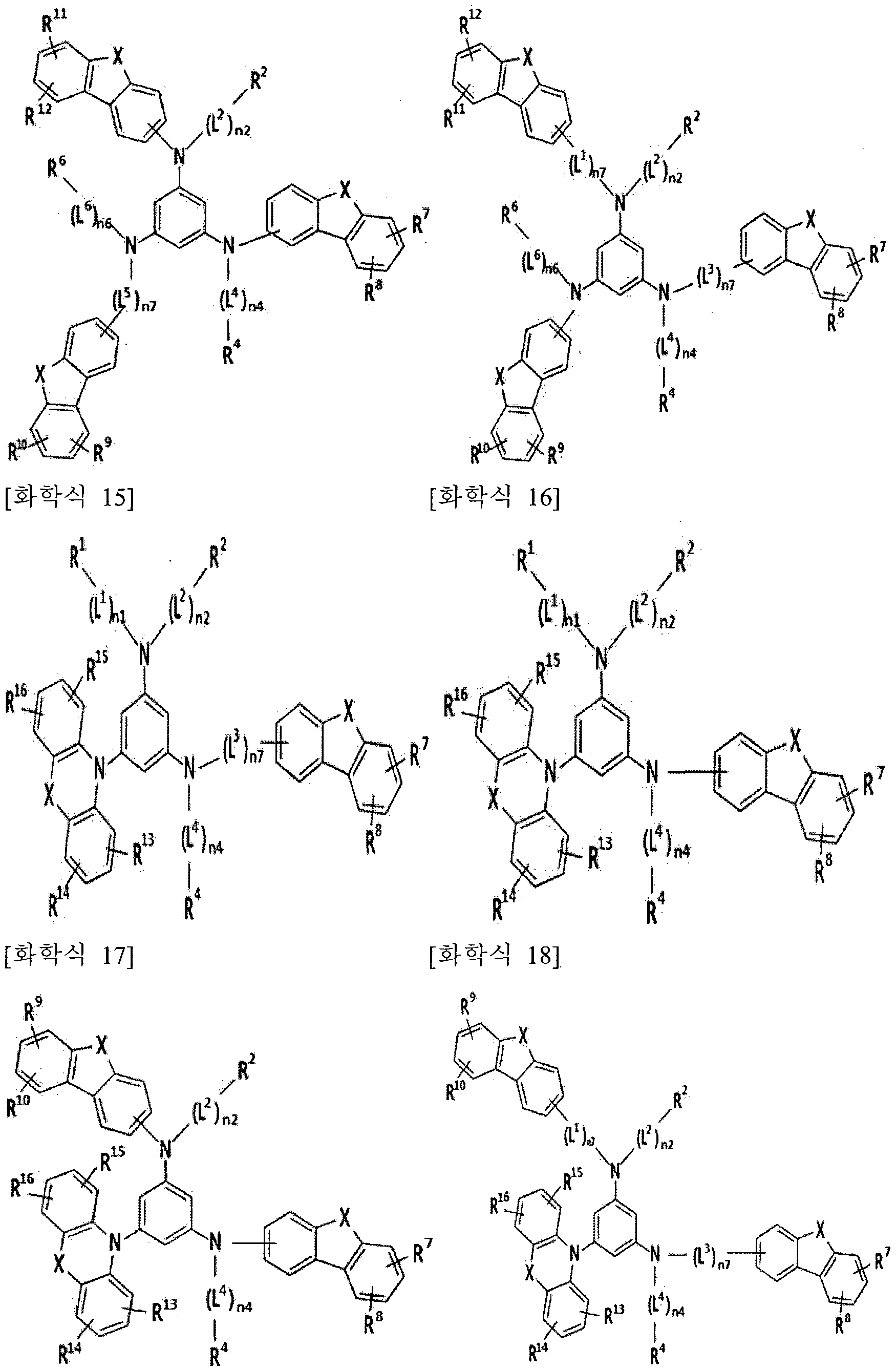
[화학식 19] [화학식 20] 정정용지 (규칙 제 91조) ISA/KR


[화학식 25] [화학식 26] 정 정 용지 (규칙 제 91 조) ISA/KR

상기 화학식 3의 L3, 상기 화학식 8의 L1 및 L2, 상기 화학식 9의 L1 및 L3, 상기 화학식 10의 L2, 상기 화학식 11의 L3, 상기 화학식 12의 L L3, 및 L5, 상기 화학식 13의 L5, 상기 화학식 14의 L' 및 L3, 상기 화학식 15의 L3, 상기 화학식 18의 L1 및 L3, 상기 화학식 19의 L3, 상기 화학식 20의 L3 및 L4, 상기 화학식 21의 L3, 상기 화학식 22의 L3, 상기 화학식 24의 L' 및 L3, 상기 화학식 25의 L3 및 L4, 상기 화학식 27의 L3, 및 상기 화학식 28의 L3 및 L4는 서로 독립적으로, 치환 또는 비치환된 C6 내지 C30 아릴렌기 , 또는 치환 또는 비치환된 C2 내지 C30 헤 테로아릴렌기 일 수 있고, 치환 또는 비치환된 플루오레닐 렌기는 아니다.
상기 L1 내지 L6는 서로 독립 적으로, 치환 또는 비치환된 C6 내지 C30 아릴렌기 일 수 있고, 치환 또는 비 치환된 플루오레닐 렌기는 아니다.
본 발명의 다른 일 구현예에서는, 양극, 음극 및 상기 양극과 음극 사이 에 개재되는 한 층 이상의 유기 박막층을 포함하고, 상기 유기박막층 중 적어도 어느 한 층은 전술한 본 발명 의 일 구현예에 따른 화합물을 포함하는 것 인 유기발광소자를 제공한다.
상기 유기 박막층은 전자주입층, 전자수송층, 정공주입층, 정공수송층, 보조 정공수송층, 또는 발광층일 수 있다.
상기 유기박막층은 정공주입층 또는 정공수송층일 수 있다.
상기 유기박막층은 보조 정공수송층일 수 있다.
상기 유기박막층은 발광층일 수 있다.
상기 화합물은 발광층 내 호스트로 이용될 수 있다.
본 발명의 또 다른 일 구현예에서는, 전술한본 발명의 일 구현예인 유기발광소자를 포함하는 표시장치를 제공한다.
【유리한 효과】
본 발명의 일 구현예에 따른 화합물을 포함하는 유기광전자소자는 우수한 전기화학적 및 열적 안정성을 가지고 수명 특성이 우수하며, 낮은 구동전압에서도 높은 발광효율을 가질 수 있다. 또한, 상기 화합물은 용액 공정에 적합할 수 있다.
【도면의 간단한 설명】
도 1 및 도 2는 본 발명의 일 구현예에 따른 유기발광소자에 대한 다양한 구현예들을 나타내는 단면도이다.
도 3은 실시예 1에 따른 화합물인 A-34에 대한 1H-NMR결과이다.
도 4는 실시예 1에 따른 화합물인 A-34에 대한 PL(photoluminescence) 파장 측정 결과이다.
<도면의 주요 부분에 대한 부호의 설명 >
100, 200: 유기발광소자 Π0: 음극
120: 양극 105: 유기박막층
130: 발광층 140: 정공 수송층
230: 발광층 + 전자 수송층
【발명의 실시를 위한 최선의 형태】
이하, 본 발명의 구현예를 상세히 설명하기로 한다. 다만, 이는 예시로서 제시되는 것으로, 이에 의해 본 발명이 제한되지는 않으며 본 발명은 후술할 청구범위의 범주에 의해 정의될 뿐이다.
본 명세서에서 "치환 "이란 별도의 정의가 없는 한, 치환기 또는 화합물 중의 적어도 하나의 수소가 중수소, 할로겐기, 히드록시기, 아미노기, 치환 또는 비치환된 C1 내지 C30 아민기, 니트로기, 치환 또는 비치환된 C1 내지 C40실릴기, C1 내지 C30 알킬기, C1 내지 C10 알킬실릴기, C3 내지 C30
시클로알킬기, C6 내지 C30 아릴기, C1 내지 C20 알콕시기, 풀루오로기, 트리플루오로메틸기 등의 C1 내지 C10 트리플루오로알킬기 또는 시아노기로 치환된 것을 의미한다.
또한 상기 치환된 할로겐기, 히드록시기, 아미노기, 치환 또는 비치환된 C1 내지 C20 아민기, 니트로기, 치환또는 비치환된 C3 내지 C40 실릴기, C1 내지 C30 알킬기, C1 내지 C10 알킬실릴기, C3 내지 C30 시클로알킬기, C6 내지 C30 아릴기, C1 내지 C20 알콕시기, 플투오로기, 트리플루오로메틸기 등의 C1 내지 C10 트리플루오로알킬기 또는 시아노기 중 인접한 두 개의 치환기가 융합되어 고리를 형성할 수도 있다. 구체적으로, 상기 치환된 C6 내지 C30 아릴기는 인접한 또다른 치환된 C6 내지 C30 아릴기와 융합되어 치환 또는 비치환된 플루오렌 고리을 형성할 수 있다.
본 명세서에서 "헤테로 "란 별도의 정의가 없는 한, 하나의 작용기 내에 N, 0,S 및 P로 이루어진 군에서 선택되는 헤테로 원자를 1 내지 3개 함유하고, 나머지는 탄소인 것을 의미한다.
본 명세서에서 "알킬 (alkyl)기"이란 별도의 정의가 없는 한, 지방족
탄화수소기를 의미한다. 알킬기는 어떠한 이중결합이나 삼증결합을 포함하고 있지 않은 "포화 알킬 (saturated alkyl)기 ' '일 수 있다.
상기 알킬기는 C1 내지 C20인 알킬기일 수 있다. 보다 구체적으로 알킬기는 C1 내지 C10 알킬기 또는 C1 내지 C6 알킬기일 수도 있다. 예를 들어, C1 내지 C4 알킬기는 알킬쇄에 1 내지 4 개의 탄소원자가 포함되는 것을 의미하며, 메틸, 에틸, 프로필, 이소-프로필 ,η-부틸, 이소-부틸, sec-부틸 및 t-부틸로 이루어진 군에서 선택됨을 나타낸다.
상기 알킬기는 구체적인 예를 들어 메틸기, 에틸기 , 프로필기, 이소프로필기 부틸기, 이소부틸기, t-부틸기, 펜틸기, 핵실기, 시클로프로필기, 시클로부틸기, 시클로펜틸기, 시클로핵실기 등을 의미한다.
본 명세서에서 "아릴 (aryl)기"는 환형인 치환기의 모든 원소가 p-오비탈을 가지고 있으며, 이들 P-오비탈이 공액 (conjugation)을 형성하고 있는 치환기를 의미하고, 모노시클릭 또는 융합 고리 폴리시클릭 (즉, 탄소원자들의 인접한 쌍들을 나눠 가지는 고리) 작용기를 포함한다.
본 명세서에서 "헤테로아릴 (heteroaryl)기' '는 아릴기 내에 N, 0, S 및 P로 이루어진 군에서 선택되는 헤테로 원자를 1 내지 3개 함유하고, 나머지는 탄소인 것을 의미한다. 상기 헤테로아릴기가 융합고리인 경우, 각각의 고리마다 상기 헤테로 원자를 1 내지 3개 포함할 수 있다.
보다 구체적으로, 치환 또는 비치환된 C6 내지 C30 아릴기 및 /또는 치환 또는 비치환된 C2 내지 C30 헤테로아릴기는, 치환 또는 비치환된 페닐기, 치환 또는 비치환된 나프틸기, 치환 또는 비치환된 안트라세닐기, ^환 또는 비치환된 페난트릴기, 치환 또는 비치환된 나프타세닐기, 치환 또는 비치환된 피레닐기, 치환 또는 비치환된 바이페닐일기, 치환 또는 비치환된 P-터페닐기, 치환 또는 비치환된 m-터페닐기, 치환 또는 비치환된
크리세닐기, 치환 또는 비치환된 트리페닐레닐기, 치환 또는 비치환된 페릴레닐기, 치환 또는 비치환된 인데닐기, 치환 또는 비치환된 퓨라닐기, 치환 또는 비치환된 티오페닐기, 치환 또는 비치환된 피를릴기, 치환 또는 비치환된 피라졸릴기, 치환 또는 비치환된 이미다졸일기, 치환 또는 비치환된 트리아졸일기, 치환 또는 비치환된 옥사졸일기, 치환 또는 비치환된 티아졸일기, 치환 또는 비치환된 옥사디아졸일기, 치환 또는 비치환된 티아디아졸일기, 치환 또는 비치환된 피리딜기, 치환 또는 비치환된 피리미디닐기, 치환 또는 비치환된 피라지닐기, 치환 또는 비치환된 트리아지닐기, 치환 또는 비치환된 벤조퓨라닐기, 치환 또는 비치환된 벤조티오페닐기, 치환 또는 비치환된 벤즈이미다졸일기, 치환 또는 비치환된 인돌일기, 치환 또는 비치환된 퀴놀리닐기, 치환 또는 비치환된 이소퀴놀리닐기, 치환 또는 비치환된 퀴나졸리닐기, 치환 또는 비치환된 퀴녹살리닐기, 치환 또는 비치환된 나프티리디닐기, 치환 또는 비치환된 벤즈옥사진일기, 치환 또는 비치환된 벤즈티아진일기, 치환 또는 비치환된 아크리디닐기, 치환 또는 비치환된 페나진일기, 치환 또는 비치환된 페노티아진일기, 치환 또는 비치환된 페녹사진일기, 치환 또는 비치환된 플루오레닐기, 치환 또는 비치환된 카바졸일기, 치환 또는 비치환된 디벤조퓨라닐기, 치환 또는 비치환된 디벤조티오페닐기, 또는 이들의 조합일 수 있으나, 이에 제한되지는 않는다.
보다 구체적인 예를 들어, 상기 치환된 C6 내지 C30 아릴기에 포함되는 치환 또는 비치환된 플루오레닐기는 하기 화학식 30 또는 화학식 31일 수 있다.
[화학식 30] [화학식 31]

상기 화학식 30 및 화학식 31에서, R25 내지 R28은 서로 독립적으로, 수소, 중수소, 할로겐기, 히드록시기, 아미노기, 치환 또는 비치환된 C1 내지 C30 아민기, 니트로기, 치환 또는 비치환된 C1 내지 C40 실릴기, C1 내지 C30 알킬기, C1 내지 C10 알킬실릴기, C3 내지 C30 시클로알킬기, C6 내지 C30 아릴기, C1 내지 C20 알콕시기, 플투오로기, 트리풀루오로메틸기 등의 C1 내지 C10 트리플루오로알킬기 또는 시아노기이며 ,*는 탄소 원자 또는 탄소 이외의 원자와 연결되는 부분을 의미한다.
본 명세서에서, 정공 특성이란, HOMO 준위를 따라 전도 특성을 가져 양극에서 형성된 정공의 발광층으로의 주입 및 발광층에서의 이동을 용이하게 하는 특성을 의미한다. 보다 구체적으로, 전자를 밀어내는 특성과도 유사할 수 있다.
또한 전자 특성이란, LUMO 준위를 따라 전도 특성을 가져 음극에서 형성된 전자의 발광층으로의 주입 및 발광충에서의 이동을 용이하게 하는 특성올 의미한다. 보다 구체적으로 전자를 당기는 특성과도 유사할 수 있다. 본 발명의 일 구현예에서는, 하기 화학식 1로 표시되는 화합물을 제공할수 있다.
[화학식 1]

상기 화학식 1에서, L1 내지 L6는 서로 독립적으로, 치환 또는 비치환된 C6 내지 C30 아릴렌기, 또는 치환 또는 비치환된 C2 내지 C30
헤테로아릴렌기이나, 치환 또는 비치환된 플루오레닐렌기는 아니며, nl 내지 n6는 서로 독립적으로, 0 내지 3 중 어느 하나의 정수이고,
R1 내지 R6는 서로 독립적으로, 수소, 중수소, 치환 또는 비치환된 C1 내지 C30 알킬기, 치환 또는 비치환된 C3 내지 C30 시클로알킬기, 치환 또는 비치환된 C6 내지 C30 아릴기, 치환 또는 비치환된 C2 내지 C30
헤테로아릴기, 또는 치환 또는 비치환된 실릴기이며, 상기 R1 내지 R6 중 적어도 하나는 하기 화학식 2로 표시되는 치환기이다.
[화학식 2]
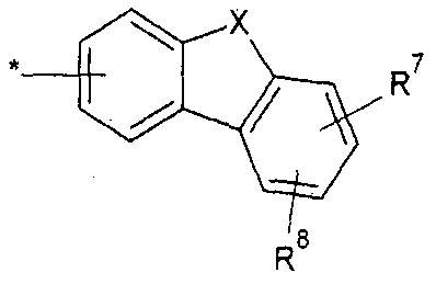
상기 화학식 2에서, X는 0 또는 S이고, R7 또는 R8은 수소, 중수소, 치환 또는 비치환된 C1 내지 C30 알킬기, 치환 또는 비치환된 C6 내지 C30 아릴기, 또는 치환 또는 비치환된 C2 내지 C30 헤테로아릴기이고, *는 탄소 원자 또는 탄소 이외의 원자와 연결되는 부분을 의미한다.
상기 화학식 1에서, R1 및 R2는 서로 독립적으로 존재하거나 서로 축합되어 축합 고리를 형성하고, R3 및 R4는 서로 독립적으로 존재하거나 서로 축합되어 축합 고리를 형성하고, R5 및 R6는 서로 독립적으로 존재하거나 서로 축합되어 축합 고리를 형성한다. 단, R1 내지 R6 중 어느 하나가 치환 또는 비치환된 플루오레닐기인 경우, 상기 치환 또는 비치환된
플루오레닐기는 상기 화학식 1의 "N"에 직 접 결합되지 않는다. 상기 본 발명의 일 구현예에 따른 화합물은 R1 내지 R6 중 적어도 하나가 상기 화학식 2로 표시되는 치환기를 가짐으로써 재료의 유리 전이 온도가 상승하여 열안정성 이 향상될 수 있으며, 정공 수송 능력 이 향상되 어 유기 발광 소자의 정공 주입 및 수송층으로 사용할 경우 구동 전압, 효율 및 수명을 향상시 킬 수 있다.
또한, 상기 화학식 1로 표시되는 화합물은 다양한 치환기를 도입함으로써 다양한 에너지 밴드 갭을 갖는 화합물이 될 수 있다.
보다 구체적으로, 상기 화학식 1은 하기 화학식 3 내지 화학식 29 증 어느 하나로 표시될 수 있다.
[화학식 3] [화학식 4]

정 정용지 (규칙 제 91조) ISA/KR

[화학식 13] [화학식 14] 정 정 용지 (규칙 제 91 조) ISA/KR

정 정 용지 (규칙 제 91 조) ISA/KR

[화학식 25] [화학식 26] 정 정 용지 (규칙 제 91 조) ISA/KR

상기 화학식 3 내지 화학식 29에서, L' 내지 L6는 서로 독립적으로, 치환 또는 비치환된 C6 내지 C30 아릴렌기 , 또는 치환 또는 비치환된 C2 내지 C30 해테로아릴렌기 일 수 있고, 치환 또는 비치환된 플루오레닐렌기는 아니며, nl 내지 n6는 서로 독립적으로, 0 내지 3 중 어느 하나의 정수일 수 있고 , n7은 1 내지 3 중 어느 하나의 정수일 수 있고, R1 내지 R6는 서로 독립적으로, 수소, 중수소, 치환 또는 비치환된 C1 내지 C30 알킬기, 치환 또는 비치환된 C3 내지 C30 시클로알킬기, 치환 또는 비치환된 C6 내지 C30 정 정용지 (규칙 제 91조) ISA/KR
아릴기, 치환또는 비치환된 C2 내지 C30 헤테로아릴기, 및 치환또는 비치환된 실릴기로 이루어진 군에서 선택될 수 있고, R1 내지 R6 중 어느 하나가 치환또는 비치환된 플루오레닐기인 경우, 상기 치환 또는 비치환된 플루오레닐기는 상기 화학식 1의 "Ν' '에 직접 결합되지 않는다.
X는 0 또는 S일 수 있고 ,R7 내지 R24는 서로 독립적으로, 수소, 중수소, 치환 또는 비치환된 C1 내지 C30 알킬기, 치환또는 비치환된 C6 내지 C30 아릴기, 및 치환 또는 비치환된 C2 내지 C30 헤테로아릴기로 이루어진 군에서 선택될 수 있다.
상기 화학식 3 내지 화학식 29의 경우, 상기 화학식 2로 표시되는 치환기를 적어도 하나 가짐으로써 재료의 유리 전이 온도가 상승하여 열안정성이 향상될 수 있으며, 정공 수송 능력이 향상되어 유기 발광 소자의 정공 주입 및 수송층으로사용할 경우 효율 및 수명을 향상시킬 수 있다.
또한, 상기 화학식 15 내지 화학식 21의 경우, 상기 화학식 2로 표시되는 치환기 외에 카바졸이 아닌 아민 화합물을 추가로 포함함으로써 HOMO 에너지 준위의 상승으로 정공 주입 장벽이 낮아져 정공 주입 특성이 향상되어, 정공 주입층으로사용할 경우 구동 전압을 낮출 수 있다.
또한, 상기 화학식 22 내지 화학식 29의 경우, 상기 화학식 2로 표시되는 치환기 외에 아민 화합물 및 /또는 카바졸릴기를 추가로 포함함으로써 내열 안정성이 향상되어 수명 특성을 향상시킬 수 있고, 높은 삼중항 에너지 준위 (T1)를 가지기 때문에 인광 발광층 호스트 또는 인광 유기 발광 소자용 정공 수송 재료로 적합한 특성을 가질 수 있다.
상기 화학식 3의 L3, 상기 화학식 8의 L1 및 L2, 상기 화학식 9의 L1 및 L3, 상기 화학식 10의 ΙΛ상기 화학식 11의 L3, 상기 화학식 12의 ΐΛ Λ및 L5, 상기 화학식 13의 L5, 상기 화학식 14와 L1 및 L3, 상기 화학식 15의 L3, 상기 화학식 18의 L1 및 L3, 상기 화학식 19의 L3, 상기 화학식 20의 L3 및 L4, 상기 화학식 21의 L3, 상기 화학식 22의 L3, 상기 화학식 24의 L' 및 L3, 상기 화학식 25의 L3 및 L4, 상기 화학식 27의 L3, 및 상기 화학식 28의 L3 및 L4는 서로 독립적으로, 치환 또는 비치환된 C6 내지 C30 아릴렌기, 또는 치환 또는 비치환된 C2 내지 C30 헤테로아릴렌기일 수 있고, 치환 또는
비치환된 플루오레닐렌기는 아니다. 보다 구체적으로 상기 L1 내지 L6는 서로 독립적으로, 치환 또는 비치환된 C6 내지 C30 아릴렌기이고, 치환 또는 비치환된 플루오레닐렌기는 제외된다. 이러한 경우, 상기 화합물은 적절한 정공 수송 특성을 가질 수 있으며, 분자량의 증가 및 재료의 packing 특성의 향상으로 인해 보다 안정한 박막을 형성할 수 있다.
또한, 상기 L1 내지 L6를 선택적으로 조절하여 화합물 전체의
공액 (conjugation) 길이를 결정할 수 있으며, 이로부터 삼중항 (triplet) 에너지 밴드갭을 조절할 수 있다. 이를 통해 유기광전자소자에서 필요로 하는 재료의 특성을 구현해 낼 수 있다. 또한, 올소 (ortho), 파라 (para), 메타 (meta)의 결합위치 변경을 통해서도 삼중항 에너지 밴드갭을 조절할 수 있다.
상기 L1 내지 L6의 구체적인 예로는 치환 또는 비치환된 페닐렌기, 치환 또는 비치환된 바이페닐렌기, 치환 또는 비치환된 P-터페닐렌기, 치환 또는 비치환된 m-터페닐렌기, 치환 또는 비치환된 0-터페닐렌기, 치환 또는 비치환된 나프틸렌기, 치환 또는 비치환된 안트라세닐렌기, 치환 또는 비치환된 페난트릴렌기, 치환 또는 비치환된 피레닐렌기 등이 있으나, 이에 제한되는 것은 아니다.
상기 R1 내지 R6는 서로 독립적으로, 수소, 치환 또는 비치환된 C6 내지 C30 아릴기일 수 있다. 이러한 경우, 화합물의 정공 및 /또는 전자 특성을 적절하게 조절할 수 있으며, 밴드갭 및 발광 파장을 조절하여 정공 수송 재료뿐만 아니라 발광층 재료로 사용할 수,있다.
상기 R1 내지 R6의 구체적인 예로는 수소, 치환 또는 비치환된 페닐기, 치환 또는 비치환된 바이페닐기, 치환 또는 비치환된 나프틸기, 치환 또는 비치환된 안트라세닐기, 치환 또는 비치환된 페난트레닐기, 치환 또는 비치환된 트리페닐기, 또는 치환 또는 비치환된 플루오레닐기 등이 있으나, 상기 R1 내지 R6가 치환 또는 비치환된 플루오레닐기인 경우, 상기 화학식 1, 및 화학식 3 내지 화학식 29에서 치환 또는 비치환된 플루오레닐기는 "N"에 직접 결합되지 않는다.
본 발명의 일 구현예에 따른 화합물의 구체적인 예는다음과 같으나, 이에 제한되는 것은 아니다.

sc oo/cioiax/i3d ££0£6l/tlOZ ΟΛΧ
24


Sei.00/£lOZH¾/I3d

9Z
εεοεόΐ/ι-ιοε OAV sc oo/cioza¾/x3i


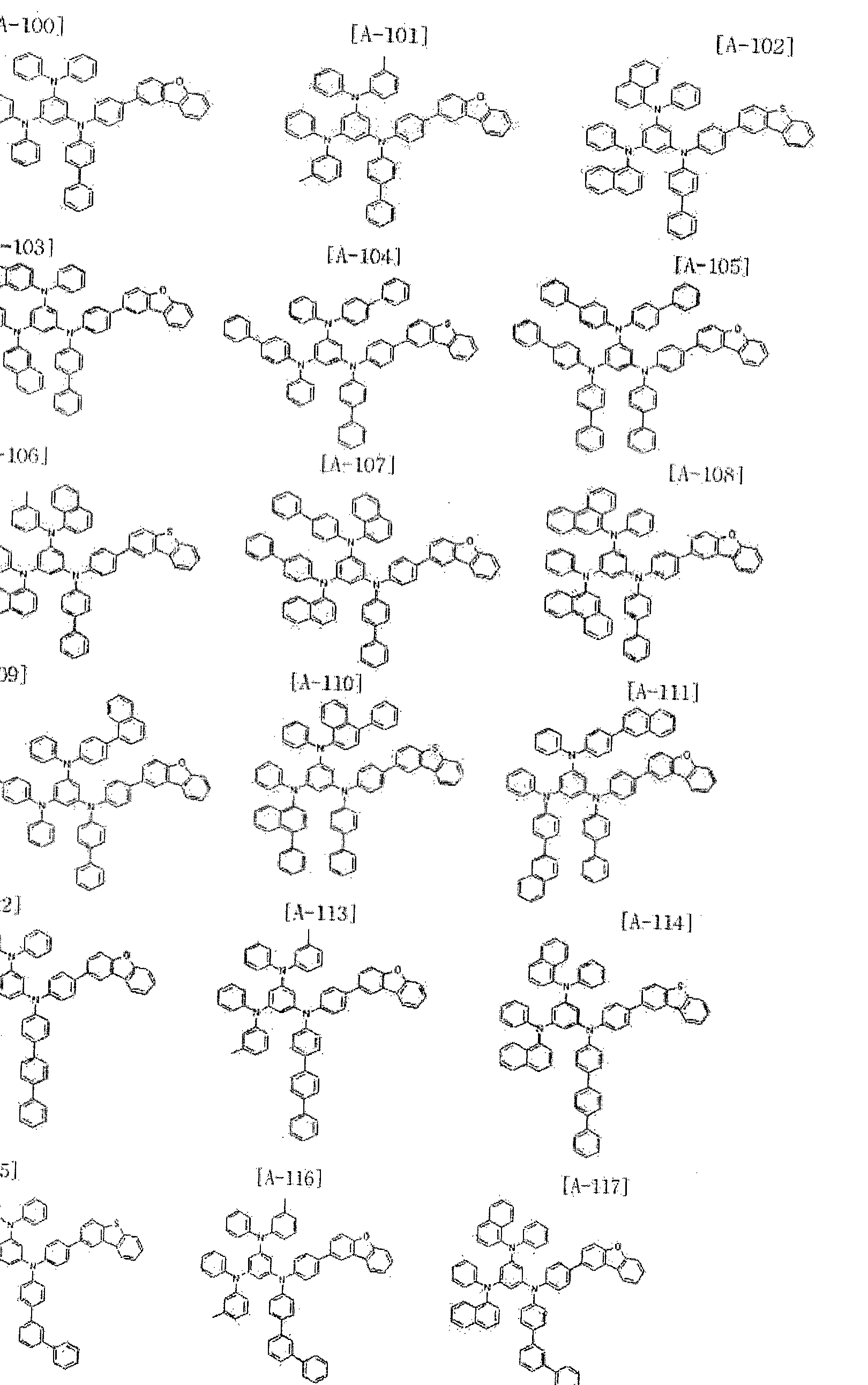
6Z
Se 00/£l0ZH¾/13d

οε
sci.oo/ciozaM/x3d εεοε6ΐ/ θζ OAV
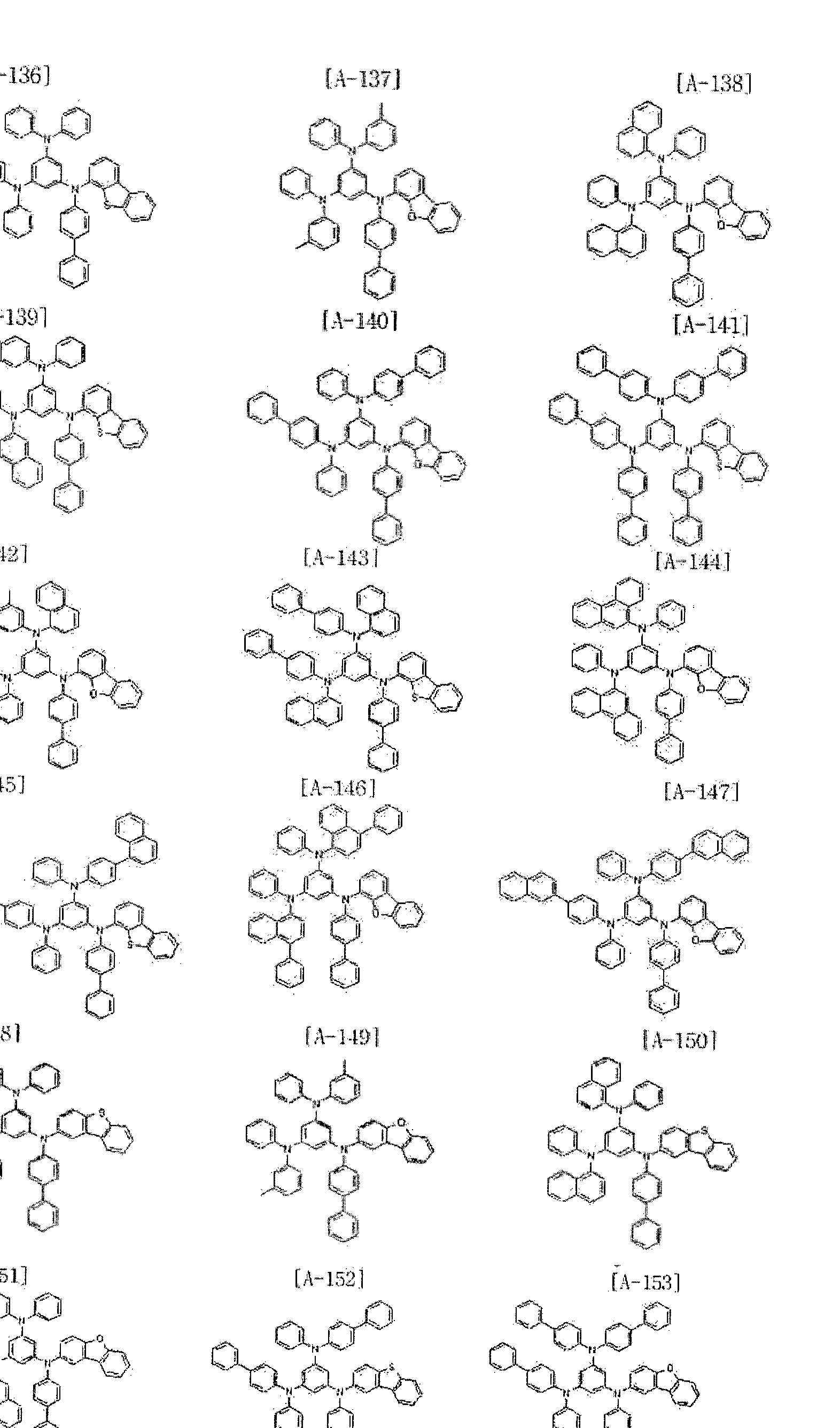
τε
εεοε6ΐ/ θζ OAV

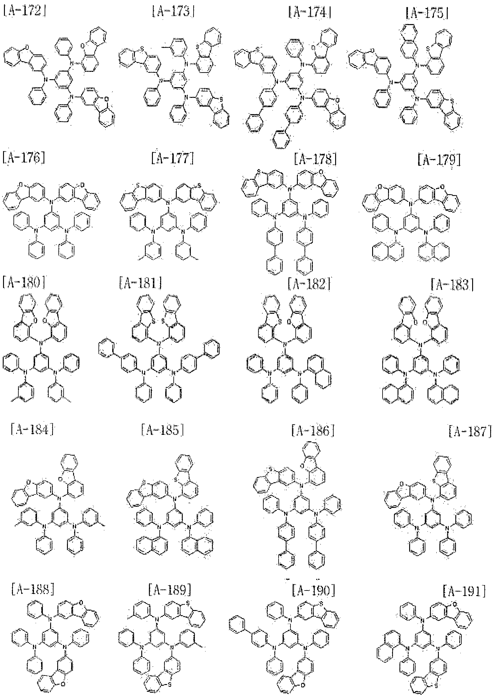


SCl.00/CT0ZaM/X3d εεοε6ΐ/ θζ OAV


Ot7
SCl.00/CT0ZaM/X3d εεοε6ΐ/ θζ OAV
41


SCl.00/CT0ZaM/X3d εεοε6ΐ/ θζ OAV

44


본 발명의 다른 일 구현예에서는, 양극, 음극 및 상기 양극과 음극 사이에
개재되는 한 층 이상의 유기박막층을 포함하고, 상기 유기박막층 중 적어도 어느 한 층은 상기 본 발명의 일 구현예에 따른 화합물을 포함하는 것인 유기광전자소자를 제공한다.
상기 유기광전자소자용 화합물은 유기박막층에 사용되어 유기광전자소자의 수명 특성, 효율 특성, 전기화학적 안정성 및 열적 안정성을 향상시키며, 구동전압을 낮출 수 있다.
상기 유기박막충은 구체적으로, 정공주입층, 정공수송층, 보조 정공수송층, 또는 발광층일 수 있다.
상기 유기광전자소자는 유기발광소자, 유기 광전 소자, 유기태양전지, 유기트랜지스터, 유기 감광체 드럼 또는 유기메모리소자일 수 있다.
보다 구체적으로, 상기 유기광전자소자는 유기발광소자일 수 있다. 도 1 또는 도 2는 본 발명의 일 구현예에 따른 화합물을 포함하는
유기발광소자의 단면도이다.
도 1 또는 도 2를 참조하면, 본 발명의 일 구현예에 따른 유기발광소자 (100 및 200)는 양극 (120), 음극 (110) 및 이 양극과 음극사이에 개재된 적어도 1층의 유기박막층 (105)을 포함하는 구조를 갖는다.
상기 양극 (120)은 양극 물질을 포함하며, 이 양극 물질로는통상
유기박막층으로 정공주입이 원활할 수 있도록 일 함수가 큰 물질이 바람직하다. 상기 양극 물질의 구체적인 예로는 니켈, 백금, 바나듬, 크롬, 구리, 아연, 금과 같은 금속 또는 이들의 합금을 들 수 있고, 아연산화물, 인듐산화물, 인듬주석산화물 (ΓΓΟ), 인듬아연산화물 (IZO)과 같은 금속 산화물을 들 수 있고, ZnO와 A1또는 Sn02와 Sb와 같은 금속과 산화물의 조합을 들 수 있고, 폴리 (3-메틸티오펜), 플리 (3,4- (에틸렌 -1,2- 디옥시)티오펜) (polyehtylenedioxythiophene: PEDT), 폴리피를 및 폴리아닐린과 같은 전도성 고분자 등을 들 수 있으나, 이에 한정되는 것은 아니다.
바람직하게는 상기 양극으로 ITO(indium tin oxide)를 포함하는 투명전극을 사용할 수 있다.
상기 음극 (110)은 음극 물질을 포함하여, 이 음극 물질로는 통상
유기박막층으로 전자주입이 용이하도톡 일 함수가 작은 물질인 것이
바람직하다. 음극 물질의 구체적 인 예로는 마그네슘, 칼슘, 나트륨, 칼륨, 타이타늄, 인듬, 이트륨, 리튬, 가돌리늄, 알루미늄, 은, 주석, 납, 세슘, 바륨 등과 같은 금속 또는 이들의 합금을 들 수 있고, LiF/Al, Li02/Al, LiF/Ca, LiF/Al 및 BaF2/Ca과 같은 다층 구조 물질 등을 들 수 있으나, 이에 한정되 는 것은 아니 다. 바람직하게는 상기 음극으로 알루미늄 등과 같은 금속전극을 사용할 수 있다.
먼저 도 1을 참조하면, 도 1은 유기박막층 (105)으로서 발광층 (130)만이 존재하는 유기 발광소자 (100)를 나타낸 것으로, 상기 유기 박막층 (105)은 발광층 (130)만으로 존재할 수 있다.
도 2를 참조하면, 도 2는 유기 박막층 (105)으로서 전자수송층을 포함하는 발광층 (230)과 정공 수송층 (140)이 존재하는 2층형 유기발광소자 (200)를 나타낸 것으로, 도 2에 나타난 바와 같이 , 유기 박막층 (105)은 발광층 (230) 및 정공수송층 (140)을 포함하는 2층형 일 수 있다. 이 경우 발광층 (130)은 전자수송층의 기 능을 하며, 정공수송층 (140)은 ίΤΟ와 같은 투명 전극과의 접합성 및 정공수송성을 향상시 키는 기능을 한다. 또한, 도 1 또는 도 2에서 유기박막층 (105)은 도시하지는 않았지만 전자주입층, 전자수송층, 보조 전자수송층, 보조 정공수송층, 또는 정공주입층 등을 추가로 포함할 수 있다. 상기 도 1 또는 도 2에서 상기 유기 박막층 (105)을 이루는 발광층 (130, 230), 정공수송층 (140), 도시하지는 않았지 만 추가될 수 있는 보조 정공수송층, 전자수송층, 보조 전자수송층, 및 이들의 조합으로 이루어진 군에서
선택되는 어 느 하나는 상기 화합물을 포함한다.
특히 상기 화합물은 상기 정공수송층 (140), 보조 정공수송층, 또는
발광층 (130, 230)에 사용될 수 있고, 발광층 (130, 230)에 사용되는 경우 발광층 내에서 호스트 재료로 사용될 수 있다.
상기에서 설명 한 유기발광소자는, 기판에 양극을 형성 한 후,
진공증착법 (evaporation), 스퍼 터 링 (sputtering), 플라즈마 도금 및 이온도금과 같은 건식성 막법 ; 또는 스핀코팅 (spin coating), 침지 법 (dipping),
유동코팅 법 (flow coating)과 같은 습식성 막법 등으로 유기박막층을 형성 한 후, 그 위에 음극을 형성하여 제조할 수 있다.
본 발명의 또 다른 일 구현예에서는, 상기 유기발광소자를 포함하는 표시장치를 제공한다.
【발명의 실시를 위한 형 태】
이하에서는 본 발명 의 구체적 인 실시 예들을 제시한다. 다만, 하기에 기 재된 실시 예들은 본 발명을 구체적으로 예시하거나 설명하기 위 한 것에 불과하며, 이로써 본 발명 이 제한되 어서는 아니 된다.
(유기광전자소자용 화합물의 제조)
중간체의 합성
합성예 1: 중간체 M-1의 합성

등근바닥 플라스크에 4-디 벤조퓨란보론산 20g(94.3mmol), 1 -브로모 -4- 아이오도벤젠 26.7g (94.3mmol)을 넣고 를루엔 (313ml)을 가하여 용해시 킨 후 탄산칼륨 19.5g (141.5mmol)을 녹인 수용액 1 17ml를 첨가시 키고 교반하였다. 여기에 테트라키스트리페닐포스핀팔라듬 1.09g(0.94mmol)을 가한 후 질소분위기하에서 12시 간 동안 환류 교반 하였다. 반웅 종료 후
에 틸아세테 이트로 추출 후 추출액을 마그네슘 설페 이트로 건조 및 여과하고 여과액을 감압 농축하였다. 생성물을 n-핵산 /디클로로메탄 (9: 1 부피 비)으로 실리카 겔 컬럼 크로마토그래피로 정제하여 목적 화합물인 중간체 M— 1을 흰색 고체로 27g (수율 89%)을 수득하였다. (계산값: 322.00g/mol, 측정값: M+ = 322.09g/mol, M+2 = 324.04g/mol)
합성 예 2: 중간체 M-2의 합성

등근바닥 플라스크에 4-디 벤조티오펜보론산 21.5g(94.3mniol), 1-브로모 -4-
아이오도벤젠 26.7g (94.3mmol)을 넣고 를루엔 (313ml)을 가하여 용해시킨 후 탄산칼륨 19.5g(141.5mmol)을 녹인 수용액 117ml를 첨가시키고 교반하였다. 여기에 테트라키스트리페닐포스핀팔라듬 1.09g(0.94mmol)을 가한 후 질소분위기하에서 12시간 동안 환류 교반 하였다. 반웅 종료 후
에틸아세테이트로 추출 후 추출액을 마그네슘 설페이트로 건조 및 여과하고 여과액을 감압 농축하였다. 생성물을 n-핵산 /디클로로메탄 (9:1 부피비)으로 실리카 겔 컬럼 크로마토그래피로 정제하여 목적 화합물인 중간체 M-2를 흰색 고체로 29g (수율 91%)을 수득하였다. (계산값: 337.98g/mol, 측정값: M+ = 338.04g/mol, M+2 = 340.11g/mol)
합성예 3: 중간체 M-3의 합성

등근바닥 플라스크에 4-클로로페닐보론산 14.7g(94.3mmol), 2- 브로모디벤조퓨란 23.3g(94.3mmol)을 넣고 를루엔 (313ml)을 가하여 용해시킨 후 탄산칼륨 19.5g(141.5mmol)을 녹인 수용액 117ml를 첨가시키고
교반하였다. 여기에 테트라키스트리페닐포스핀팔라듐 1.09g(0.94mmol)을 가한 후 질소분위기하에서 12시간 동안 환류 교반하였다. 반응 종료 후
에틸아세테이트로 추출 후 추출액을 마그네슘 설페이트로 건조 및 여과하고 여과액을 감압 농축하였다. 생성물을 n-핵산 /디클로로메탄 (9:1 부피비)으로 실리카 겔 컬럼 크로마토그래피로 정제하여 목적 화합물인 중간체 M-3를 흰색 고체로 23.9g (수율 91%)을 수득하였다. (계산값: 278.05g/mol, 측정값: M+ = 278.12g/mol, M+2 = 280.13g/mol)
합성예 4: 중간체 M-4의 합성

에 틸아세 테 이트로 추출 후 추출액을 마그네슘 설페 이트로 건조 및 여과하고 여과액을 감압 농축하였다. 생성물을 n—핵산 /디클로로메탄 (9: 1 부피 비)으로 실리카 겔 컬럼 크로마토그래피로 정제하여 목적 화합물인 증간체 M-4를 흰색 고체로 25.6g (수율 92%)을 수득하였다. (계산값: 294.03g/mol, 측정 값: M+ = 294.16g/mol, M+2 = 296.13g/mol)

등근바닥 플라스크에 중간체 M-1 10g(30.9mmol)과 4-아미노바이페닐
6.3g(37.08mmol), 소디움 t-부특사이드 5.35g(55.6mmol)을 넣고 를루엔 155ml을 가하여 용해시 켰다. 여기 에 Pd(dba)2 0.178g (0.31mmol)과 트리 -터셔 리 - 부틸포스핀 0.125g(0.62mmol)을 차례로 넣은 후 질소 분위기 하에서 4시간 동안 환류 교반 시 킨다. 반웅 종료 후 에 틸아세테 이트과 증류수로 추출 후 유기층을 마그네슘 설페이트로 건조, 여과하고 여과액을 감압 농축하였다. 생성물을 n-핵산 /디클로로메탄 (7:3 부피 비) 으로 실리카 겔 컬럼
크로마토그래피로 정 제하여 목적 화합물인 중간체 M-5를 흰색 고체로
9.92g (수율 78%)을 수득하였다. (계산값 : 41 U6g/mol, 측정 값: M+ = 41 1.21g/mol) 합성 예 6: 중간체 M-6의 합성

등근바닥 플라스크에 중간체 M-4 9.1g(30.9mmol)과 4-아미노바이페닐
6.3g(37.08mmol), 소디움 t-부록사이드 5.35g(55.6mmol)을 넣고 톨루엔 155ml을 가하여 용해 시 켰다. 여기에 Pd(dba)2 0.178g (0.31mmol)과 트리 -터셔 리- 부틸포스핀 0.125g(0.62mmol)을 차례로 넣은 후 질소 분위기 하에서 4시간 동안 환류 교반 시 킨다. 반웅 종료 후 에 틸아세테이트과 증류수로 추출 후 유기층을 마그네슴 설페이트로 건조, 여과하고 여과액을 감압 농축하였다. 생성물을 n-핵산 /디클로로메탄 (7:3 부피비) 으로 실리카 겔 컬럼
크로마토그래피로 정제하여 목적 화합물인 중간체 M-6을 흰색 고체로
10.6g (수율 80%)을 수득하였다. (계산값: 427.14g/mol, 측정값: M+ = 427.19g/mol) 합성 예 7: 중간체 M-7의 합성
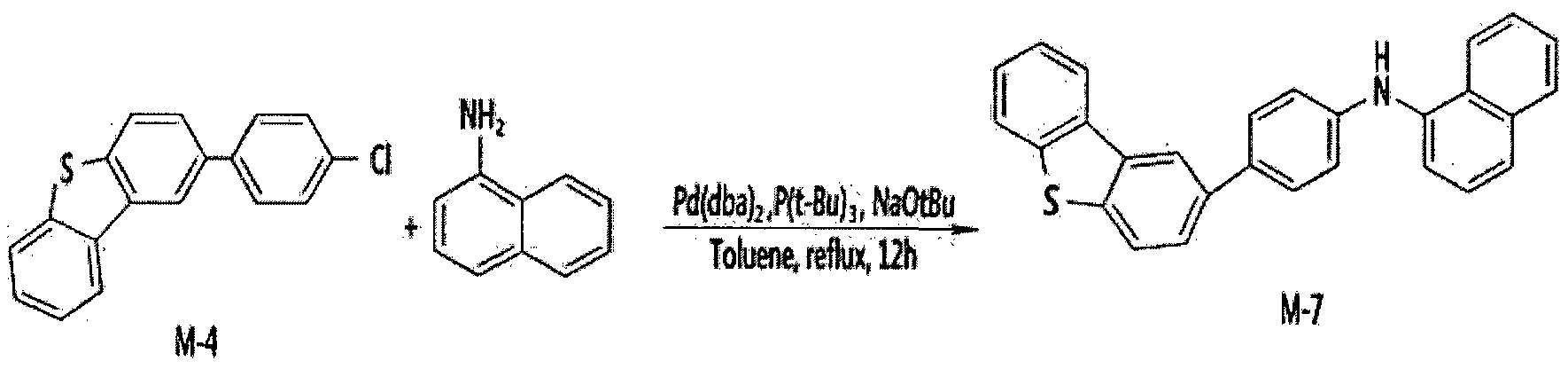
등근바닥 플라스크에 중간체 M-4 9.1g(30.9mmol)과 1-아미노나프탈렌
5.3g(37.08mmol), 소디움 t-부특사이드 5.35g(55.6mmol)을 넣고 를루엔 155ml을 가하여 용해시 켰다. 여기에 Pd(dba)2 0.178g (0.31mmol)과 트리 -터셔 리- 부틸포스핀 0.125g(0.62mmol)을 차례로 넣은 후 질소 분위기 하에서 12시간 동안 환류 교반 시킨다. 반웅 종료 후 에틸아세테이트과 증류수로 추출 후 유기층을 마그네슴 설페이트로 건조, 여과하고 여과액을 감압 농축하였다. 생성물을 n-핵산 /디클로로메탄 (7:3 부피비) 으로 실리카 겔 컬 럼
크로마토그래피로 정제하여 목적 화합물인 중간체 M-7을 흰색 고체로
10g (수율 81%)을 수득하였다. (계산값: 401.12g/mol, 측정 값: M+ = 40L15g/mol) 합성 예 8: 중간체 M-8의 합성
정 정용지 (규칙 제 91조) ISA/KR

등근바닥 플라스크에 중간체 M-2 31.9g(64.7mmol)과 아세트아미드
1.74g(29.4mmol), 탄산칼륨 17.3g(l .6mmol)을 넣고 자일렌 130ml을 가하여 용해 시 켰다. 여기에 요오드화구리 (I) 1.12g (5.88mmol)과 Ν,Ν- 다메틸에 틸렌디아민 1.04g(11.8mmol)을 차례로 넣은 후 질소 분위기 하에서 48시간 동안 환류 교반 시 킨다. 반응 종료 를루엔과 증류수로 추출 후 유기층을 마그네슴 설페 이트로 건조, 여과하고 여과액을 감압 농축하였다. 생성물을 n-핵산 /에틸아세테 이트 (7:3 부피비)으로 실리카 겔 컬럼
크로마토그래피로 정제하여 목적 화합물인 M-8을 14g (수율 93%)을
수득하였다. (계산값: 575.14g/mol, 측정값: M+ = 575.3 lg/mol)
합성 예 9: 중간체 M-9의 합성

4.2g(75.6mmol)을 넣고 테트라하이드로퓨란 80ml와 에탄올 80mL을 가하여 용해 시 켰다. 질소 분위기 하에서 12시간 동안 환류 교반 시 킨다. 반응 종료 반웅액을 감압 농축한 후 디클로메탄과 증류수로 추출 후 유기층을
마그네슘 설페 이트로 건조, 여과하고 여과액을 감압 농축하였다. 생성물을 n- 핵산 /디클로로메탄 (7:3 부피비)으로 실리카 겔 컬럼 크로마토그래피로 정제하여 목적 화합물인 M-9를 12.1g (수율 90%)을 수득하였다. (계산값:
533.13g/mol, 측정 값: M+ = 533.26g/mol)
합성 예 10: 중간체 M-10의 합성
정정용지 (규칙 제 91조) ISA/KR

등근바닥 플라스크에 1,3-디브로모 -5-클로로벤젠 25g(92.47mmoi)과 디페닐아민 31.3g(184.9mmol), 소디움 t-부톡사이드 26.7g(277.41mmol)을 넣고 를루엔 463ml을 가하여 용해시 켰다. 여기에 Pd(dba)2 0.266g (0.462mmol)과 트리-터셔 리 -부틸포스핀 0.187g(0.924mmol)을 차례로 넣은 후 질소 분위기 하에서 4시간 동안 환류 교반 시킨다. 반응 종료 후 에틸아세테 이트과 증류수로 추출 후 유기층을 마그네슘 설페이트로 건조, 여과하고 여과액을 감압 농축하였다. 생성물을 n-핵산 /디클로로메탄 (9:1 부피비) 으로 실리카 겔 컬럼 크로마토그래피로 정제하여 목적 화합물인 중간체 M-10을 흰색 고체로 34 g (수율 84%)을 수득하였다. (계산값: 446.15g/mol, 측정 값: M+ =
446.23g/mol)
합성 예 11: 중간체 M-11의 합성

등근바닥 플라스크에 1,3-디브로모 -5-클로로벤젠 25g(92.47mmol)과 3- 메틸디페닐아민 33.9g(184.9mmol), 소디움 t-부톡사이드 26.7g(277.41mmol)을 넣고 를루엔 463ml을 가하여 용해시켰다. 여기 에 Pd(dba)2 0.266g
(0.462mmol)과 트리-터셔 리 -부틸포스핀 0.187g(0.924mmol)을 차궤로 넣은 후 질소 분위기 하에서 4시간 동안 환류 교반 시 킨다. 반웅 종료 후
에틸아세테이트과 증류수로 추출 후 유기층을 마그네슘 설페 이트로 건조, 여과하고 여과액을 감압 농축하였다. 생성물을 n-핵산 /디클로로메탄 (9:1 부피비) 으로 실리카 겔 컬럼 크로마토그래피로 정제하여 목적 화합물인 중간체 M-11을 흰색 고체로 37.3g (수율 85%)을 수득하였다. (계산값: 정 정용지 (규칙 제 91조) ISA/KR
474.19g/mol, 측정값: M+ = 474.28g/mol)
합성 예 12: 중간체 M-12의 합성

등근바닥 플라스크에 1,3-디브로모 -5-클로로벤젠 25g(9247mmol)과 바이페닐- 4—일 -페닐 아민 45.4g(184.9mmol), 소디움 t-부톡사이드 26.7g(277.41mmol)을 넣고 를루엔 463ml을 가하여 용해시켰다. 여 기에 Pd(dba)2 0.266g
(0.462mmol)과 트리-터셔 리—부틸포스핀 0.187g(0.924mmol)을 차례로 넣은 후 질소 분위기 하에서 4시간 동안 환류 교반 시킨다. 반웅 종료 후
에 틸아세테 이트과 증류수로 추출 후 유기층을 마그네슘 설페 이트로 건조, 여과하고 여과액을 감압 농축하였다. 생성물을 n-핵산 /디클로로메탄 (8:2 부피 비) 으로 실리카 겔 컬럼 크로마토그래피로 정제하여 목적 화합물인 중간체 M-12를 흰색 고체로 44.9g (수율 81%)을 수득하였다. (계산값:
598.22g/mol, 측정 값: M+ = 598.37g/mol)
합성예 13: 중간체 M-13의 합성

등근바닥 플라스크에 1,3-디브로모 -5—클로로벤젠 25g(92.47mmol)과 페녹사진 33.9g(184.9mmol), 소디움 t-부톡사이드 26.7g(277.41mmol)을 넣고 를루엔 463ml을 가하여 용해시 켰다. 여기에 Pd(dba)2 0.266g (0.462mmol)과 트리- 터셔 리 -부틸포스핀 (U87g(0.924mmol)을 차례로 넣은 후 질소 분위기 하에서 4시간 동안 환류 교반 시킨다. 반응 종료 후 에 틸아세테이트과 증류수로 추출 후 유기층을 마그네슴 설페이트로 건조, 여과하고 여과액을 감압 농축하였다. 생성물을 n-핵산 /디클로로메탄 (8:2 부피비) 으로 실리카 겔 컬럼 정 정용지 (규칙 제 91조) ISA/KR
크로마토그래피로 정제하여 목적 화합물인 중간체 M-13을 흰색 고체로 36.9g (수율 84%)을 수득하였다. (계산값 : 474.11g/mol, 측정값: M+ =
474.26g/mol)
합성 예 14: 중간체 M-14의 합성

등근바닥 플라스크에 1,3-디브로모 -5-클로로벤젠 25g(92.47mmol)과 카바졸 30.9g(184.9mmol), 소디움 t-부특사이드 26 g(277.41mmol)을 넣고 를루엔 463 ml을 가하여 용해시 켰다. 여기 에 Pd(dba)2 0.266g (0.462mmol)과 트리- 터셔 리 -부털포스핀 0.187g(0.924mmol)을 차례로 넣은 후 질소 분위기 하에서 4시간 동안 환류 교반 시 킨다. 반웅 종료 후 에 틸아세테 이트과 증류수로 추출 후 유기층을 마그네슘 설페이트로 건조, 여과하고 여과액을 감압 농축하였다. 생성물을 n-핵산 /다클로로메탄 (8:2 부피비) 으로 실리카 겔 컬럼 크로마토그래피로 정제하여 목적 화합물인 중간체 M-14를 흰색 고체로 33.2g (수율 81%)을 수득하였다. (계산값 : 442.12g/m0l, 측정값: M+ =
442.36g/mol)
합성예 15: 중간체 M-15의 합성

등근바닥 플라스크에 1-브로모 -3,5-디클로로벤젠 25g(92.47mmol)과 카바졸 15.5g(92.47mmol), 소디움 t-부톡사이드 13.4g(138.7mmol)을 넣고 톨루엔 463ml을 가하여 용해 시 켰다. 여기에 Pd(dba)2 0.133g (0.231mmol)과 트리- 터셔리 -부틸포스핀 0.094g(0.462mmol)을 차례로 넣은 후 질소 분위기 하에서 시간 동안 환류 교반 시 킨다. 반웅 종료 후 에 틸아세테이트과 증류수로 정 정용지 (규칙 제 91조) ISA/KR
추출 후 유기층을 마그네슘 설페이트로 건조, 여과하고 여과액을 감압 농축하였다. 생성물을 n-핵산 /디클로로메탄 (9:1 부피비) 으로 실리카 겔 컬럼 크로마토그래피로 정제하여 목적 화합물인 중간체 M-15를 흰색 고체로 24.0g (수율 83%)을 수득하였다. (계산값 : 311.03g/mol, 측정값: M+ =
311.17g/mol)
합성예 16: 중간체 M-16의 합성

등근바닥 플라스크에 1-브로모 -3,5—디클로로벤젠 25g(92 7mmol)과 페녹사진 16.9g(92.47mmol), 소디움 t-부록사이드 13.4g(138.7mmol)을 넣고 를루엔 463ml을 가하여 용해시켰다. 여기에 Pd(dba)2 0.133g (0.231mmol)과 트리 - 터셔리 -부틸포스핀 0.094g(0.462mmol)을 차례로 넣은 후 질소 분위기 하에서 4시간 동안 환류 교반 시킨다. 반웅 종료 후 에틸아세테 이트과 증류수로 추출 후 유기층을 마그네슴 설페 이트로 건조, 여과하고 여과액을 감압 농축하였다. 생성물을 n-핵산 /디클로로메탄 (8:2 부피 비) 으로 실리카 겔 컬럼 크로마토그래피로 정제하여 목적 화합물인 증간체 M-16을 흰색 고체로 25.7g (수율 85%)을 수득하였다. (계산값 : 327.02g/mol, 측정 값: M+ =
327.27g/mol)
합성 예 17: 중간체 M-17의 합성

M-2
둥근바닥 플라스크에 중간체 M-2 10.5g(30.9mmol)과 4-아미노바이페닐 6.3g(37.08mmol), 소디움 t-부톡사이드 5.35g(55.6mmol)을 넣고 를루엔 155ml을 가하여 용해 시 켰다. 여 기에 Pd(dba)2 0.178g (0.31mmol)과 트리 -터셔 리 - 부틸포스핀 0.125g(0.62mmol)을 차례로 넣은 후 질소 분위기 하에서 4시간 정 정용지 (규칙 제 91조) ISA/KR
동안 환류 교반 시 킨다. 반웅 종료 후 에 틸아세테 이트과 증류수로 추출 후 유기층을 마그네슘 설페 이트로 건조, 여과하고 여과액을 감압 농축하였다. 생성물을 n-핵산 /디클로로메탄 (7:3 부피 비) 으로 실리카 겔 컬럼
크로마토그래피로 정제하여 목적 화합물인 증간체 M-17을 흰색 고체로 9.91g (수율 75%)을 수득하였다.
(계산값: 427.14g/mol, 측정 값: M+ = 427.29g/mol)
합성 예 18: 중간체 M-18의 합성

등근바닥 플라스크에 중간체 2-브로모디 벤조퓨란 7.6g(30.9mmol)과 4- 아미노바이 페닐 6.3g(37.08mmol), 소디움 t-부특사이드 5.35g(55.6mmol)을 넣고 를루엔 155ml을 가하여 용해 시 켰다. 여기에 Pd(dba)2 0.178g (0.31mmol)과 트리-터셔 리 -부틸포스핀 0.125g(0.62rmnol)을 차례로 넣은 후 질소 분위기 하에서 4시간 동안 환류 교반 시 킨다. 반응 종료 후 에 틸아세테 이트과 증류수로 추출 후 유기층을 마그네슘 설페 이트로 간조, 여과하고 여과액을 감압 농축하였다. 생성물을 n-핵산 /디클로로메탄 (7:3 부피 비) 으로 실리카 겔 컬럼 크로마토그래피로 정 제하여 목적 화합물인 중간체 M- 18을 흰색 고체로 8.1g (수율 78%)을 수득하였다.
(계산값: 335.13g/mol, 측정 값: M+ = 335.42g/mol)
합성 예 19: 중간체 M-19의 합성

등근바닥 플라스크에 증간체 2-브로모디 벤조티오펜 8.1g(30.9mmol)과 2- 아미 노나프탈렌 5.3g(37.08mmol), 소디움 t-부톡사이드 5.35g(55.6mmol)을 넣고 를루엔 155ml을 가하여 용해시 켰다. 여기에 Pd(dba)2 i78g (0.3 hnmol)과 트리 -터셔 리ᅳ부틸포스핀 0.125g(0.62mmol)을 차례로 넣은 후 질소 분위기
하에서 4시 간 동안 환류 교반 시 킨다. 반응 종료 후 에 틸아세테 이트과 증류수로 추출 후 유기층을 마그네슘 설페 이트로 건조, 여과하고 여과액을 감압 농축하였다. 생성물을 η-핵산 /디클로로메 탄 (7:3 부피 비) 으로 실리카 겔 컬럼 크로마토그래피로 정 제하여 목적 화합물인 중간체 M-19을 흰색 고체로 7.9g (수율 79%)을 수득하였다.
(계산값: 325.09g/mol, 측정값: M+ = 325.33g/mol)
합성 예 20: 중간체 M-20의 합성
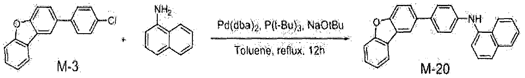
둥근바닥 플라스크에 중간체 M-3 8.6g(30.9mmol)과 1-아미노나프탈렌 5.3g(37.08mmol), 소디움 t-부록사이드 5.35g(55.6mmol)을 넣고 톨루엔 155ml을 가하여 용해 시 켰다. 여 기에 Pd(dba)2 0.178g (0.31mmol)과 트리 -터셔 리- 부틸포스핀 0.125g(0.62mmol)을 차례로 넣은 후 질소 분위기 하에서 12시간 동안 환류 교반 시 킨다. 반응 종료 후 에 틸아세테 이트과 증류수로 추출 후 유기층을 마그네슘 설페 이트로 건조, 여과하고 여과액을 감압 농축하였다. 생성물을 II-핵산 /디클로로메탄 (7:3 부피 비) 으로 실리카 겔 컬럼
크로마토그래피로 정 제하여 목적 화합물인 중간체 M-20을 흰색 고체로 9.5g (수율 80%)을 수득하였다.
(계산값: 385.15g/mol, 측정 값: M+ = 385.27g/mol)
합성 예 21: 중간체 M-21의 합성

등근바닥 플라스크에 M-15 28.9g(92.47mmol)과 페녹사진 16.9g(92.47mmol): 소디움 t-부록사이드 13.4g(138.7mmol)을 넣고 를루엔 463ml을 가하여
용해시 켰다. 여기에 Pd(dba)2 0.133g (0.231mmol)과 트리 -터셔 리 -부틸포스핀 0.094g(0.462mmol) 을 차례로 넣은 후 질소 분위 기 하에서 12시간 동안 환류 교반 시 킨다. 반웅 종료 후 에 틸아세테 이트과 증류수로 추출 후 유기층을 마그네슘 설페 이트로 건조, 여과하고 여과액을 감압 농축하였다. 생성물을 n- 핵산 /디클로로메탄 (8:2 부피 비) 으로 실리카 겔 컬럼 크로마토그래피로 정 제하여 목적 화합물인 중간체 M-21을 흰색 고체로 35.6g (수율 81%)을 수득하였다.
(계산값: 474.10g/mol, 측정 값: M+ = 474.38g/mol)
합성 예 22: 중간체 M-22의 합성

등근바닥 플라스크에 M-15 28.9g(92.47mmol)과 바이페닐 -4-일 -페 닐 아민 22.7g(92.47mmol), 소디움 t-부특사이드 13.4g(138.7mmol)을 넣고 롤루엔 463ml을 가하여 용해시 켰다. 여기 에 Pd(dba)2 0.133g (0.231mmol)과 트리 - 터셔 리ᅳ부틸포스핀 0.094g(0.462mmol) 을 차례로 넣은 후 질소 분위기 하에서 12시 간 동안 환류 교반 시 킨다. 반응 종료 후 에 틸아세테이트과 증류수로 추출 후 유기층을 마그네슘 설페이트로 건조, 여과하고 여과액을 감압 농축하였다. 생성물을 n-핵산 /디클로로메탄 (8:2 부피 비) 으로 실리카 겔 ¾럼 크로마토그래피로 정 제하여 목적 화합물인 중간체 M-22을 흰색 고체로 38.1g (수율 79%)을 수득하였다.
(계산값: 520.17g/mol, 측정값: M+ = 520.36g/mol)
유기광전소자용 화합물의 합성
상기에 기 재 된 화학식 A- 1 내지 A-300, B-1 내지 B-20, C-1 내지 C-12, D- 1 내지 D-8, E-1 내지 E-28, 및 F-1 내지 F-20은 하기 일반식 1 내지 6의 합성 방법에 따라 제조할 수 있다. 본 발명 의 일 구현예에 따른 구체 화합물들올 하기 [표 1]에 나타내었다.
ί일반식 11 Α-1 내지 A-291, 및 A-300 화합물의 합성
[일반식 1-1]

[일반식 1-2]

【일반식 2ᅵ B-l 내지 B-20 화합물의 합성
[일반식 2-1]
정 정 용지 (규칙 제 91조) ISA/KR

[일반식 2-2]

[일반식 3-1]

정 정 용지 (규칙 제 91 조) ISA/KR

【일반식 4Π -1 내지 D-8 화합물의 합성

I일반식 51 E-1 내지 E-28 화합물의 합성 [일반식 5-1]

[일반식 5-2]

정 정용지 (규칙 제 91 조) ISA/KR
【일반식 6ᅵ F-l 내지 F-20 화합물의 합성

[표 i]

정 정 용지 (규칙 제 91조) ISA/KR

정 정 용지 (규칙 제 91 조) ISA/KR
 실시 예 1: 화합물 A-34의 합성
상기 화합물 A-34를 하기 반웅식 ί과 같은 경로를 통해 합성하였다. [반응식 1]

등근바닥 플라스크에 증간체 M-10 10g(22.37mmol)과 중간체 M-5
9.2g(22.37mmol), 소디움 t-부톡사이드 3.2g(33.56mmol)을 넣고 를루엔 250ml을 가하여 용해 시켰다. 여기에 Pd(dba)2 0.129g (0.224mmol)과 트리 -터셔 리- 부틸포스핀 0.091g(0.448mmol)을 차례로 넣은 후 질소 분위기 하에서 12시간 동안 환류 교반 시킨다. 반웅 종료 후 를루엔과 증류수로 추출 후 유기층을
정 정용지 (규칙 제 91조) ISA/KR
마그네슴 설페이트로 건조, 여과하고 여과액을 감압 농축하였다. 생성물을 n- 핵산 /디클로로메탄 (8:2 부피비) 으로 실리카 겔 컬럼 크로마토그래피로 정제하여 목적 화합물인 A-34를 흰색 고체로 16.9g (수율 92%)을 수득하였다.
(계산값: 821.34g/mol, 측정값: M+ = 821.46g/mol)
실시 예 2: 화합물 A-104의 합성
상기 화합물 A-104를 하기 반웅식 2를 통해 합성하였다.
[반웅식 2]

둥근바닥 플라스크에 증간체 M-12 13.4g(22.37mmol)과 중간체 M-6
9.6g(22.37mmol), 소디움 t-부톡사이드 3.2g(33.56mmol)을 넣고 톨루엔 250ml을 가하여 용해 시 켰다. 여기에 Pd(dba)2 0.129g (0.224mmol)과 트리 -터셔 리- 부틸포스핀 0.091g(0.448mmol)을 차례로 넣은 후 질소 분위기 하에서 12시간 동안 환류 교반 시킨다. 반응 종료 후 를루엔과 증류수로 추출 후 유기층을 마그네슴 설페이트로 건조, 여과하고 여과액을 감압 농축하였다. 생성물을 n- 핵산 /디클로로메탄 (8:2 부피 비) 으로 실리카 겔 컬럼 크로마토그래피로 정제하여 목적 화합물인 A-104를 흰색 고체로 20.6g (수율 93%)을 수득하였다. (계산값: 989.38g/mol, 측정 값: M+ = 989.45g/mol)
실시 예 3: 화합물 A-201의 합성
상기 화합물 A-2()l를 하기 반웅식 3을 통해 합성하였다.
[반웅식 3]
정 정용지 (규칙 제 91조) ISA/KR
 Exact Mass: 971.34
Mol. Wt: 972.27 둥근바닥 플라스크에 중간체 M-11 10.6g(22.37mmol)과 중간체 M-9 11.9g (22.37mmol), 소디움 t-부톡사이드 3.2g(33.56mmol)을 넣고 를루엔 250ml을 가하여 용해시 켰다. 여기에 Pd(dba)2 0.129g (0.224mmol)과 트리 -터셔 리 - 부틸포스핀 0.091g(0.448mmol)을 차례로 넣은 후 질소 분위기 하에서 12시간 동안 환류 교반 시 킨다. 반웅 종료 후 를루엔과 증류수로 추출 후 유기층을 마그네슴 설페 이트로 건조, 여과하고 여과액을 감압 농축하였다. 생성물을 n- 핵산 /디클로로메탄 (8:2 부피비)으로 실리카 겔 컬럼 크로마토그래피로 정제하여 목적 화합물인 A-201을 흰색 고체로 19.8g (수율 91%)을 수득하였다.
(계산값: 971.34g/mol, 측정 값: M+ = 971.51g/mol)
실시 예 4: 화합물 A-88의 합성
상기 화합물 A-88을 하기 반웅식 4를 통해 합성하였다.
[반웅식 4]

등근바닥 플라스크에 중간체 M-10 10g(22.37mmol)과 중간체 M-7 9.0g
(22.37mmol), 소디음 t-부톡사이드 3.2g(33.56mmol)을 넣고 를루엔 250ml을 가하여 용해시켰다. 여기에 Pd(dba)2 0.129g (0.224mmol)과 트리 -터셔 리 - 부틸포스핀 0.091g(0.448mmol)을 차례로 넣은 후 질소 분위기 하에서 12시간 동안 환류 교반 시 킨다. 반웅 종료 후 틀루엔과 증류수로 추출 후 유기층을 마그네슴 설페이트로 건조, 여과하고 여과액을 감압 농축하였다. 생성물을 n- 핵산 /디클로로메탄 (8:2 부피비)으로 실리카 겔 컬럼 크로마토그래피로
정 정용지 (규칙 제 91조) ISA/KR
정제하여 목적 화합물인 A-88을 흰색 고체로 16.5g (수율 91%)을 수득하였다. (계산값: 811.30g/mol, 측정값: M+ = 811.61g/mol)
실시 예 5: 화합물 B-17의 합성
상기 화합물 B-17을 하기 반웅식 5를 통해 합성하였다.
[반웅식 5]

등근바닥 플라스크에 증간체 M-16 7.3g(22.37mmol)과 중간체 M-19 14.6g (44.74mmol), 소다움 t-부톡사이드 6.4g(67.Hmmol)을 넣고 를루엔 250ml을 가하여 용해시 켰다. 여기에 Pd(dba)2 0.258g (0.448mmol)과 트리 -터셔 리- 부틸포스핀 0.182g(0.896mmol)을 차례로 넣은 후 질소 분위기 하에서 12시간 동안 환류 교반 시킨다. 반웅 종료 후 를루엔과 증류수로 추출 후 유기층을 마그네슘 설페 이트로 건조, 여과하고 여과액을 감압 농축하였다. 생성물을 n- 핵산 /디클로로메탄 (8:2 부피 비)으로 실리카 겔 컬럼 크로마토그래피로 정제하여 목적 화합물인 B-17을 연노랑색 고체로 19.1g (수율 94%)을 수득하였다.
(계산값: 905.25g/mol, 측정 값: M+ = 905.49g/mol)
실시 예 6: 화합물 C-8의 합성
상기 화합물 C-8을 하기 반웅식 6를 통해 합성하였다.
[반웅식 6]

정 정용지 (규칙 제 91 조) ISA/KR
등근바닥 플라스크에 증간체 M-13 10.6g(22.37mmol)과 중간체 M-20 8.6g (22.37mmol), 소디움 t-부톡사이드 3.2g(33.56mmol)을 넣고 를루엔 250ml을 가하여 용해시 켰다. 여기에 Pd(dba)2 0.129g (0.224mmol)과 트리 -터셔 리- 부틸포스핀 0.091g(0.448mmol)을 차례로 넣은 후 질소 분위기 하에서 12시간 동안 환류 교반 시 킨다. 반응 종료 후 롤루엔과 증류수로 추출 후 유기층을 마그네슴 설페이트로 건조, 여 과하고 여과액을 감압 농축하였다. 생성물을 n- 핵산 /디클로로메탄 (S:2 부피비)으로 실리카 겔 컬럼 크로마토그래피로 정제하여 목적 화합물인 C-8을 흰색 고체로 17g (수율 92%)을 수득하였다.
(계산값: 823.28g/mol, 측정값: M+ = 823.41g/mol)
실시 예 7: 화합물 D-6의 합성
상기 화합물 D-6을 하기 반웅식 7을 통해 합성하였다.
[반응식 7]

등근바닥 플라스크에 증간체 M-21 10.6g(22.37mmol)과 중간체 M-18 7.5g (22.37mmol), 소디움 t-부톡사이드 3.2g(33.56mmol)을 넣고 를루엔 250ml을 가하여 용해시 켰다. 여기에 Pd(dba)2 0.129g (0.224mmol)과 트리 -터셔 리- 부틸포스핀 0.091g(0.448mmol)을 차례로 넣은 후 질소 분위 기 하에서 12시간 동안 환류 교반 시 킨다. 반응 종료 후 를루엔과 증류수로 추출 후 유기층을 마그네슘 설페 이트로 건조, 여과하고 여과액을 감압 농축하였다. 생성물을 n- 핵산 /디클로로메탄 (8:2 부피 비)으로 실리카 겔 컬럼 크로마토그래피로 정제하여 목적 화합물인 D-6을 연노란색 고체로 16.1g (수율 93%)을
수득하였다.
(계산값: 773.25g/mol, 측정 값: M+ = 773.5 lg/mol)
실시 예 8: 화합물 E-25의 합성
정 정용지 (규칙 제 91조) ISA/KR
상기 화합물 E-: 하기 반웅식 8을 통해 합성하였다.
[반응식 8]

등근바닥 플라스크에 중간체 M-22 l l g(22.37mmol)과 중간체 M-5 9.2g (22.37mmol), 소디움 t-부톡사이드 3.2g(33.56mmol)을 넣고 를루엔 250ml을 가하여 용해시 켰다. 여기에 Pd(dba)2 0.129g (0.224mmol)과 트리 -터셔 리- 부틸포스핀 0.091g(0.448mmol)을 차례로 넣은 후 질소 분위 기 하에서 12시간 동안 환류 교반 시킨다. 반웅 종료 후 를루엔과 증류수로 추출 후 유기층을 마그네슴 설페이트로 건조, 여과하고 여과액을 감압 농축하였다. 생성물을 n- 핵산 /디클로로메탄 (8:2 부피비 )으로 실리카 겔 컬럼 크로마토그래피로 정제하여 목적 화합물인 E-25를 흰색 고체로 18g (수율 90%)을 수득하였다.
(계산값: 895.36g/mol, 측정 값: M+ = 895.48g/mol)
실시 예 9: 화합물 F-2의 합성
상기 화합물 F— 2를 하기 반웅식 9를 통해 합성하였다.
[반웅식 9]

등근바닥 플라스크에 중간체 M-14 9.9g(22.37mmol)과 중간체 M-17 9.6g (22.37mmol), 소디움 t-부톡사이드 3.2g(33.56mmol)을 넣고 를루엔 250ml을 가하여 용해시켰다. 여기에 Pd(dba)2 0.129g (0.224mmol)과 트리 -터셔 리 - 부틸포스핀 0.091g(0.448mmol)을 차례로 넣은 후 질소 분위기 하에서 12시간
정 정용지 (규칙 제 91조) ISA/KR
동안 환류 교반 시 킨다. 반웅 종료 후 를루엔과 증류수로 추출 후 유기층을 마그네슴 설페 이트로 건조, 여과하고 여과액을 감압 농축하였다. 생성물을 η- 핵산 /디클로로메탄 (8:2 부피 비)으로 실리카 겔 컬럼 크로마토그래피로 정 제하여 목적 화합물인 F-2를 흰색 고체로 17.5g (수율 94%)올 수득하였다. (계산값: 833.29g/mol, 측정값: M+ = 833.42g/mol)
(제조된 화합물의 분석 및 특성 측정)
1) 분자량 측정
화합물의 구조 분석을 위해 LC-MS를 이용하여 분자량을 측정하였다.
2) 1H-NMR 결과 분석
화합물의 구조 분석을 위해 상기 실시 예 1에 따른 화합물을 CD2C12용매에 녹인 다음 300MHz NMR 장비를 이용하여 1H— NMR을 측정하였다. 그 결과를 도 3에 나타내었다.
3) 형 광 특성 분석
형 광 특성을 측정하기 위 해서 상기 실시 예 1에 따른 화합물올 THF에 녹인 후 HITACHI F-4500을 이용하여 PL(photoluminescence) 파장을 측정하였다. 그 결과를 도 4에 나타내었다.
(유기발광소자의 제조)
녹색 유기 발광 소자의 제조
실시 예 10
ΠΌ (Indium tin oxide)가 1500A의 두께로 박막 코팅 된 유리 기판을 증류수 초음파로 세척하였다. 증류수 세척 이 끝나면 이소프로필 알코을, 아세톤, 메탄올 등의 용제로 초음파 세척을 하고 건조시 킨 후 플라즈마 세정기로 이송시 킨 다음 산소 플라즈마를 이용하여 상기 기판을 5분간 세정 한 후 진공 층착기로 기판을 이송하였다. 이 렇게 준비된 ΠΌ 투명 전극을 양극으로 사용하여 ITO 기판 상부에 Ν,Ν'-디 (1-나프틸) -Ν,Ν'-디페닐벤지 딘 [NPB]을 진공 증착하여 700Α 두께의 정공주입 및 수송층을 형성하였다. 이어서 실시 예 1에서 제조된 Α-34 화합물을 사용하여 진공 증착으로 100A 두께의 보조 정공수송층을 형성하였다. 상기 보조 정공수송충 상부에 (4,4'-Ν,Ν'- 디카바졸)비 페닐 [CBP]를 호스트로 사용하고 도편트로 트리스 (2-
페닐피리딘)이리듬 (III)[Ir(ppy)3]를 5중량 %로 도핑하여 진공 중착으로 300 A 두께의 발광층을 형성하였다.
그 후 상기 발광층 상부에 비페녹시 -비스 (8- 히드록시퀴놀린)알루미늄 [Balq]을 진공 중착하여 50A 두께의 정공저지층을 형성하였다. 상기 정공저지층 상부에 트리스 (8- 히드록시퀴놀린)알루미늄 [Alq3]을 진공 증착하여 250 A 두께의 전자수송층을 형성하고 상기 전자수송층 상부에 LiF lOA과 A11000A을 순차적으로 진공 증착하여 음극을 형성함으로써 유기발광소자를 제조하였다.
상기 유기발광소자는 5층의 유기박막층을 가지는 구조로 되어 있으며, 구체적으로
Al(1000A)/LiF(10A)/Alq3(250A)/Balq(50A)/EML[CBP:Ir(ppy)3=95:5](300A)/A- 34(100 A)/NPB(700A)/ITO(1500A)의 구조로 제작하였다.
실시예 11
상기 실시예 10에서, 실시예 1에서 제조된 화합물 (Α-34) 대신 실시예 2에서 제조된 화합물 (A-104)을사용한 점을 제외하고는 동일한 방법으로 유기발광소자를 제조하였다.
실시예 12
상기 실시예 10에서, 실시예 1 에서 제조된 화합물 (Α-34) 대신 실시예 3에서 제조된 화합물 (A-201)을사용한 점을 제외하고는 동일한 방법으로 유기발광소자를 제조하였다.
실시예 13
상기 실시예 10에서, 실시예 1에서 제조된 화합물 (Α-34) 대신 실시예 7에서 제조된 화합물 (D-6)을 사용한 점을 제외하고는 동일한 방법으로
유기발광소자를 제조하였다.
실시예 14
상기 실시예 10에서, 실시예 1에서 제조된 화합물 (Α-34) 대신 실시예 8에서 제조된 화합물 (Ε-25)을 사용한 점을 제외하고는 동일한 방법으로
유기발광소자를 제조하였다.
실시예 15
상기 실시예 10에서, 실시예 1에서 제조된 화합물 (A-34) 대신 실시예 9에서 제조된 화합물 (F-2)을사용한 점을 제외하고는 동일한 방법으로
유기발광소자를 제조하였다.
비교예 1
상기 실시예 10에서, 실시예 1에서 제조된 화합물 (A-34) 대신 Ν,Ν'-디 (1- 나프틸) -Ν,Ν'-디페닐벤지딘 [ΝΡΒ]를사용한 점을 제외하고는 동일한 방법으로 유기발광소자를 제조하였다.
비교예 2
상기 실시예 10에서, 실시예 1에서 제조된 화합물 (Α-34) 대신 TDAB를 사용한 점을 제외하고는 동일한 방법으로 유기발광소자를 제조하였다. 적색 유기 발광소자의 제조
실시예 16
ITO (Indium tin oxide)가 1500A의 두께로 박막 코팅된 유리 기판을 증류수 초음파로 세척하였다. 증류수 세척이 끝나면 이소프로필 알코올, 아세톤, 메탄을 등의 용제로 초음파 세척을 하고 건조시킨 후 풀라즈마 세정기로 이송시킨 다음 산소 플라즈마를 이용하여 상기 기판을 5분간 세정한후 진공 층착기로 기판을 이송하였다. 이렇게 준비된 ITO 투명 전극을 양극으로 사용하여 ΠΌ 기판 상부에 4,4'-bis[N-[4-{N,N-bis(3-methylphenyl)amino}- phenyl]-N-phenylamino]biphenyl[DNTPD]를 진공 증착하여 600 A두께의 정공 주입층을 형성하였다. 이어서 Ν,Ν'-디 (1-나프틸) -Ν,Ν'-디페닐벤지딘 [NPB]을 진공 증착으로 200Α 두께의 정공수송층을 형성하였다. 상기 정공수송층 상부에 실시예 1에서 제조된 화합물 Α-34를 사용하여 진공 증착으로 1Q0A 두께의 보조 정공수송층을 형성하였다. 상기 보조 정공수송층 상부에 (4,4'- Ν,Ν'-디카바졸)비페닐 [CBP]를 호스트로 사용하고 도편트로 비스 (2- 페닐퀴놀린) (아세틸아세토네이트)이리듐 (III)[Ir(pq)2acac]를 7증량0 /。로 도핑하여 진공 증착으로 300 A 두께의 발광층을 형성하였다.
그 후 상기 발광층 상부에 비페녹시—비스 (8- 히드록시퀴놀린)알루미늄 [Balq]을 진공 증착하여 50A 두께의 정공저지층을 형성하였다. 상기 정공저지층 상부에 트리스 (8-
히드록시퀴놀린)알루미늄 [Alq3]을 진공 증착하여 250A 두께의 전자수송층을 형성하고 상기 전자수송층 상부에 LiF lOA과 A11000A을 순차적으로 진공 증착하여 음극을 형성함으로써 유기발광소자를 제조하였다.
상기 유기발광소자는 6층의 유기박막층을 가지는 구조로 되어 있으며, 구체적으로 Al(1000A)/LiF(10A)/Alq3(250A)/Balq(50A)/EML[CBP: Ir(pq)2acac =93:7](300A)/A-34(100A)/NPB(700A)/DNTPD(600A)/ITO(1^ 구조로 제작하였다.
실시예 17
상기 실시예 16에서, 실시예 1에서 제조된 화합물 (A-34) 대신 실시예 2에서 제조된 화합물 (A-104)을 사용한 점을 제외하고는 동일한 방법으로 유기발광소자를 제조하였다.
실시예 18
상기 실시예 16에서, 실시예 1에서 제조된 화합물 (A-34) 대신 실시예 4에서 제조된 화합물 (A-88)올 사용한 점을 제외하고는 동일한 방법으로
유기발광소자를 제조하였다.
실시예 19
상기 실시예 16에서, 실시예 1에서 제조된 화합물 (A-34) 대신 실시예 5에서 제조된 화합물 (B-17)을 사용한 점을 제외하고는 동일한 방법으로
유기발광소자를 제조하였다.
실시예 20
상기 실시예 16에서, 실시예 1에서 제조된 화합물 (A-34) 대신 실시예 6에서 제조된 화합물 (C-8)을 사용한 점을 제외하고는 동일한 방법으로
유기발광소자를 제조하였다.
실시예 21
상기 실시예 16에서, 실시예 1에서 제조된 화합물 (A-34) 대신 실시예 8에서 제조된 화합물 (E-25)을 사용한 점을 제외하고는 동일한 방법으로
유기발광소자를 제조하였다.
실시예 22
상기 실시예 16에서, 실시예 1에서 제조된 화합물 (A-34) 대신 실시예 9에서
제조된 화합물 (F-2)을 사용한 점을 제외하고는 동일한 방법으로
유기발광소자를 제조하였다.
비교예 3
상기 실시예 16에서, 실시예 1에서 제조된 화합물 (A-34) 대신 Ν,Ν'-디 (1- ' 나프틸) -Ν,Ν'-디페닐벤지딘 [ΝΡΒ]를 사용한 점을 제외하고는 동일한 방법으로 유기발광소자를 제조하였다.
비교예 4
상기 실시예 16에서, 실시예 1에서 제조된 화합물 (Α-34) 대신 TDAB를 사용한 점을 제외하고는 동일한 방법으로 유기발광소자를 제조하였다.
상기 유기발광소자 제작에 사용된 DNTPD, ΝΡΒ, TDAB, CBP, Balq, Alq3, Ir(ppy)3, Ir(pq)2acac 의 구조는 아래와 같다.
상기 유기발광소자 제작에 사용된 DNTPD, NPB, TDAB, CBP, Balq, Alq3, Ir(ppy)3, Ir(pq)2acac 의 구조는 아래와 같다.

(유기발광소자의 성능 측정)
상기 실시예 10 내지 22, 및 비교예 1 내지 4에서 제조된 각각의
유기발광소자에 대하여 전압에 따른 전류밀도 변화, 휘도변화 및 발광효율을 측정하였다. 구체적인 측정방법은 하기와 같고, 그 결과는 하기 [표 2] 및 [표 3]에 나타내었다
(1) 전압변화에 따른 전류밀도의 변화 측정
제조된 유기발광소자에 대해, 전압을 0V 부터 10V까지 상승시키면서 전류-전압계 (Keithley 2400)를 이용하여 단위소자에 흐르는 전류값을 측정하고 측정된 전류값을 면적으로 나누어 결과를 얻었다. .
(2) 전압변화에 따른 휘도변화 측정
제조된 유기발광소자에 대해, 전압을 0V 부터 10V까지 상승시키면서 휘도계 (Minolta Cs-IOOOA)를 이용하여 그 때의 휘도를 측정하여 결과를 얻었다.
(3) 발광효율 측정
상기 (1) 및 (2)로부터 측정된 휘도와 전류밀도 및 전압을 이용하여 동일 휘도 (cd/m2)에서의 전류 효율 (cd/A)을 계산하였다.
(4) 수명 측정
제조된 유기발광소자에 대해 폴라로닉스 수명 측정 시스템올 사용하여 실시예 10 내지 15, 비교예 1, 및 비교예 2의 녹색 유기 발광 소자의 경우에는 초기 휘도 3,000nit로 발광시키고 시간 경과에 따른 휘도의 감소를 측정하여 초기 휘도 대비 1/2로 휘도가 감소된 시점을 반감수명으로 하였고, 실시예 16 내지 22, 비교예 3. 및 비교예 4의 적색 유기 발광 소자의 경우에는 초기 휘도 l,000nit로 발광시키고 시간 경과에 따른 휘도의 감소를 측정하여 초기 휘도 대비 80%로 휘도가 감소된 시점올 T80수명으로 측정하였다.
[표 2]


(구동전압 및 발광효율 l.OOOnit에서 측정) 상기 [표 2]의 결과에 따르면 녹색 인광 유기발광소자에서 보조
정공수송층을 사용하지 않은 비교예 1 대비 본 발명의 화합물을 보조 정공수송층으로 사용한 상기 실시예 10 내지 15는 유기발광소자의
발광효율과 수명을 향상시킴을 알 수 있다. 특히 비교예 1 대비 본 발명의 실시예는 발광효율이 최소 36%에서 최대 56% 이상 크게 상승하는 것을 알 수 있고, 종래에 알려져있는 TDAB를 보조 정공수송층으로사용한 비교예 2 대비 본 발명의 실시예는 발광 소자수명이 최소 31%에서 최대 54% 이상 상승하여 실제 소자의 상업화 측면에서 소자의 수명은 제품화의 가장 큰 문제 중 하나임을 고려할 때 상기 실시예들의 결과는 소자를 제품화하여 상업화하기에 층분한 것으로 판단된다.
[표 3]


(구동전압 및 발광효을 l.OOOnit에서 측정) 상기 [표 3]의 결과에 따르면 적색 인광 유기발광소자에서
보조정공수송층을 사용하지 않은 비교예 3 대비 본 발명의 화합물을 보조 정공수송층으로 사용한 상기 실시예 16 내지 22는 유기발광소자의
발광효율과 수명을 향상시킴을 알 수 있다. 특히 비교예 3 대비 본 발명의 실시예는 발광효율이 최소 14%에서 최대 25% 이상 크게 상승하는 것을 알 수 있고, 종래에 알려져있는 TDAB를 보조 정공수송층으로 사용한 비교예 4 대비 본 발명의 실시예는 발광효율이 최소 8%에서 최대 18% 이상상승하고: 발광 소자 수명이 최소 27%에서 최대 40% 이상상승하며, 구동전압을 낮추어 적색 인광 소자의 전반적인 주요 특성을 크게 향상 시킴을 알 수 있다.실제 소자의 상업화 측면에서 소자의 수명은 제품화의 가장 큰 문제 중 하나임을 고려할 때 상기 실시예들의 결과는 소자를 제품화하여
상업화하기에 층분한 것으로 판단된다.
본 발명은 상기 실시예들에 한정되는 것이 아니라 서로 다른 다양한 형태로 제조될 수 있으며, 본 발명이 속하는 기술분야에서 통상의 지식을 가진 자는 본 발명의 기술적 사상이나 필수적인 특징을 변경하지 않고서 다른 구체적인 형태로 실시될 수 있다는 것을 이해할 수 있을 것이다.
그러므로 이상에서 기술한 실시예들은 모든 면에서 예시적인 것이며 한정적이 아닌 것으로 이해해야만 한다.
Claims
【청구의 범위】
【청구항 1]
하기 화학식 1로 표시되는 화합물:
[화학식 1]

상기 화학식 1에서,
L' 내지 L6는 서로 독립적으로, 치환 또는 비치환된 C6 내지 C30 아릴렌기 또는 치환 또는 비치환된 C2 내지 C30 해테로아릴렌기이나, 치환 또는 비치환된 플루오레닐렌기는 아니며,
nl 내지 n6는 서로 독립적으로, 0 내지 3 중 어느 하나의 정수이고,
R1 내지 R6는 서로 독립적으로, 수소, 중수소, 치환 또는 비치환된 C1 내지 C30 알킬기, 치환 또는 비치환된 C3 내지 C30 시클로알킬기, 치환 또는 비치환된 C6 내지 C30 아릴기, 치환 또는 비치환된 C2 내지 C30 헤테로아릴기, 및 치환또는 비치환된 실릴기로 이루어진 군에서 선택되고, 상기 R1 내지 R6 중 적어도 하나는 하기 화학식 2로 표시되고,
[화학식 2]

상기 화학식 2에서,
X는 0 또는 S이고,
R7 또는 R8은 수소, 증수소, 치환 또는 비치환된 C1 내지 C30 알킬기, 치환 또는 비치환된 C6 내지 C30 아릴기, 및 치환 또는 비치환된 C2 내지 C30
헤테로아릴기로 이루어진 군에서 선택되고,
*는 탄소 원자 또는 탄소 이외의 원자와 연결되는 부분을 의미하고, R1 및 R2는 서로 독립적으로 존재하거나 서로 축합되어 축합 고리를 형성하고,
R3 및 R4는 서로 독립적으로 존재하거나 서로 축합되 어 축합 고리를 형성하고,
R5 및 R6는 서로 독립적으로 존재하거나 서로 축합되어 축합 고리를 형성 한다.
(단, R1 내지 R6 중 어느 하나가 치환 또는 비치환된 플루오레닐기 인 경우, 상기 치환 또는 비치환된 플루오레닐기는 상기 화학식 1의 "N"에 직 접 결합되지 않는다)
【청구항 2】
제 1항에 있어서,
상기 화학식 1은 하기 화학식 3 내지 화학식 14 증 어느 하나로 표시되는 화합물:
[화학식 3] [화학식 4]

[화학식 5] [화학식 6]
정 정용지 (규칙 제 91조) ISA/KR

[화학식 9]


정정용지 (규칙 제 91조) ISA/KR

비치환된 플루오레닐렌기는 아니며 ,
nl 내지 n6는 서로 독립적으로, 0 내지 3 중 어느 하나의 정수이고, n7은 1 내지 3 증 어느 하나의 정수이고,
R1 내지 R6는 서로 독립적으로, 수소, 중수소, 치환 또는 비치환된 C1 내지 C30 알킬기, 치환 또는 비치환된 C3 내지 C30 시클로알킬기 , 치환 또는 비치환된 C6 내지 C30 아릴기 , 치환 또는 비치환된 C2 내지 C30
헤테로아릴기 , 및 치환 또는 비치환된 실릴기로 이루어진 군에서 선택되고,
X는 0 또는 S이고,
R7 내지 R12은 서로 독립적으로, 수소, 중수소, 치환 또는 비치환된 C1 내 C30 알킬기, 치환 또는 비치 환된 C6 내지 C30 아릴기 , 및 치환 또는 정 정용지 (규칙 제 91조) ISA/KR
비치환된 C2 내지 C30 해테로아릴기로 이루어진 군에서 선택된다. (단, 상기 R1 내지 R6 중 어느 하나가 치환 또는 비치환된 플루오레닐기 인 경우, 상기 치환 또는 비치환된 플루오레닐기는 상기 화학식 1의 "N"에 직접 결합되지 않는다)
【청구항 3]
제 1항에 있어서 ,
상기 화학식 1은 하기 화학식 15 내지 화학식 18 중 어느 하나로 표시되는 화합물:
[화학식 15] [화학식 16]

상기 화학식 15 내지 18에서 ,
L1 내지 L4는 서로 독립적으로, 치환 또는 비치환된 C6 내지 C30 아릴렌기 또는 치환 또는 비치환된 C2 내지 C30 헤 테로아릴렌기 이나, 치환 또는 비치환된 플루오레닐렌기는 제외 되며,
nl 내지 n4는 서로 독립적으로, 0 내지 3 중 어느 하나의 정수이고,
정 정용지 (규칙 제 91조) ISA/KR
n7은 1 내지 3 중 어느 하나의 정수이고,
R1, R2, 및 R4는 서로 독립적으로, 수소, 중수소, 치환 또는 비치환된 C1 내지 C30 알킬기, 치환 또는 비치환된 C3 내지 C30 시클로알킬기, 치환 또는 비치환된 C6 내지 C30 아릴기 , 치환 또는 비치환된 C2 내지 C30 헤테로아릴기 , 및 치환 또는 비치환된 실릴기로 이루어진 군에서 선택되고,
X는 0 또는 S이고,
R7 내지 R10, 및 R13 내지 R16은 서로 독립적으로, 수소, 중수소, 치환 또는 비치환된 Cr 내지 C30 알킬기 , 치환 또는 비치환된 C6 내지 C30 아릴기 , 및 치환 또는 비치환된 C2 내지 C30 해테로아릴기로 이루어진 군에서 선택된다. (단, R R2, 및 R4는 중 어느 하나가 치환 또는 비치환된 플루오레닐기 인 경우, 상기 치환 또는 비치환된 플루오레 닐기는 상기 화학식 1의 에 직 접 결합되지 않는다)
【청구항 4】
저 U항에 있어서 ,
상기 화학식 1은 하기 화학식 19 내지 화학식 21 중 어느 하나로 표시되는 화합물:
[화학식 19] [화학식 2이

[화학식 21]
정 정용지 (규칙 제 91조) ISA/KR

상기 화학식 19 내지 화학식 21에서 ,
L3 및 L4는 서로 독립적으로, 치환 또는 비치환된 C6 내지 C30 아릴렌기, 또는 치환 또는 비치환된 C2 내지 C30 해테로아릴렌기 이나, 치환 또는 비치환된 플루오레닐렌기는 제외되며 ,
n4는 0 내지 3 증 어느 하나의 정수이고,
n7은 1 내지 3 중 어느 하나의 정수이고,
R4는 수소, 중수소, 치환 또는 비치환된 C1 내지 C30 알킬기, 치환 또는 비치환된 C3 내지 C30 시클로알킬기 , 치환 또는 비치환된 C6 내지 C30 아릴기 , 치환 또는 비치환된 C2 내지 C30 해테로아릴기, 및 치환 또는 비치환된 실릴기로 이루어진 군에서 선택되고,
X는 O 또는 S이고,
R7 내지 R10, 및 R13 내지 R22은 서로 독립적으로, 수소, 중수소, 치환 또는 비치환된 C1 내지 C30 알킬기, 치환 또는 비치환된 C6 내지 C30 아릴기 , 및 치환 또는 비치환된 C2 내지 C30 헤테로아릴기로 이루어진 군에서 선택된다.
(단, 상기 R4가 치환 또는 비치환된 플루오레닐기 인 경우, 상기 치환 또는 비치환된 플루오레닐기는 상기 화학식 1의 "N"에 직 접결합되지 않는다)
【청구항 5】 "
거 11항에 있어서,
상기 화학식 1은 하기 화학식 22 내지 화학식 26 중 어느 하나로 표시되는 화합물:
[화학식 22] [화학식 23]
정 정용지 (규칙 제 91조) ISA/KR

상기 화학식 22 내지 화학식 26에서,
L1 내지 L4는 서로 독립적으로, 치환 또는 비치환된 C6 내지 C30 아릴렌기 또는 치환 또는 비치환된 C2 내지 C30 헤테로아릴렌기 이나, 치환 또는 비치환된 플루오레닐렌기는 아니며 ,
nl, n2, 및 n4는 0 내지 3 중 어느 하나의 정수이고
정 정용지 (규칙 제 91조) ISA/KR
n7은 1 내지 3 중 어느 하나의 정수이고,
R1, R2, 및 R4는 수소, 증수소, 치환 또는 비치환된 C1 내지 C30 알킬기, 치환 또는 바치환된 C3.내지. C30 시클로알킬기, 치환 ^는 비치환된 6 내지 C30 아릴기, 치환 또는 비치환된 C2 내지 C30 헤테로아릴기, 및 치환 또는 비치환된 실릴기로 이루어진 군에서 선택되고,
X는 0 또는 S이고,
R7 내지 R10,R21, 및 R22은 서로 독립적으로, 수소, 중수소, 치환 또는 비치환된 C1 내지 C30 알킬기,:치환 또는 비치환된 C6 내지 C30 아릴기, 및 치환 또는 비치환된 C2 내지 C30 해테로아릴기로 이루어진 군에서 선택된다. (단, 상기 R R2, 및 R4 중 어느 하나가 치환 또는 비치환된 플루오레닐기인 경우, 상기 치환 또는 비치환된 플루오레닐기는 상기 화학식 1의 "N"에 직접 결합되지 않는다)
【청구항 6】
제 1항에 있어서,
상기 화학식 1은 하기 화학식 27 내지 화학식 29 중 어느 하나로 표시되는 화합물:
[화학식 27] [화학식 28]

[화학식 29]
정정용지 (규칙제 91조) ISA/KR

상기 화학식 27 내지 화학식 29에서,
L3 및 L4는 서로 독립적으로, 치환 또는 비치환된 C6 내지 C30 아릴렌기, 또는 치환 또는 비치환된 C2 내지 C30 헤테로아릴렌기 이나, 치환 또는 비치환된 플루오레 닐렌기는 아니고,
n4는 0 내지 3 중 어느 하나의 정수이고,
n7은 1 내지 3 중 어느 하나의 정수이고,
R4는 수소, 중수소, 치환 또는 비치환된 C1 내지 C30 알킬기 , 치환 또는 비치환된 C3 내지 C30 시클로알킬기 , 치환 또는 비치환된 C6 내지 C30 아릴기 , 치환 또는 비치환된 C2 내지 C30 해테로아릴기 , 및 치환 또는 비치환된 실릴기로 이루어진 군에서 선택되고,
X는 0 또는 S이고,
R7 내지 R10, 및 R21 내지 R24은 서로 독립적으로, 수소, 중수소, 치환 또는 비치환된 C1 내지 C30 알킬기 , 치환 또는 비치환된 C6 내지 C30 아릴기, 및 치환 또는 비치환된 C2 내지 C30 헤테로아릴기로 이루어진 군에서 선택된다.
(단, 상기 R4가 치환 또는 비치환된 플루오레닐기 인 경우, 상기 치환 또는 비치환된 플루오레 닐기는 상기 화학식 1의 "N"에 직접 결합되지 않는다)
【청구항 71
제 2항에 있어서 ,
상기 화학식 3의 L3; 상기 화학식 8의 L1 및 L2; 상기 화학식 9의 L1 및 L3; 상기 화학식 10의 L2; 상기 화학식 11의 L3; 상기 화학식 12의 ΐΛ ΐΛ 및 L5;
정 정용지 (규칙 제 91조) ISA/KR
상기 화학식 13의 L5; 및 상기 화학식 14의 L1 및 L3는 서로 독립적으로, 치환 또는 비치환된 C6 내지 C30 아릴렌기, 또는 치환 또는 비치환된 C2 내지 C30 헤테로아릴렌기이나, 치환 또는 비치환된 플루오레닐렌기는 아닌 화합물.
【청구항 8】
제 3항에 있어서,
상기 화학식 15의 L3; 및 상기 화학식 18의 L1 및 L3는 서로 독립적으로, 치환 또는 비치환된 C6 내지 C30 아릴렌기, 또는 치환 또는 비치환된 C2 내지 C30 해테로아릴렌기이나, 치환 또는 비치환된 플루오레닐렌기는 아닌 화합물.
【청구항 9】
제 4항에 있어서,
상기 화학식 19의 L3; 상기 화학식 20의 L3 및 L4; 및 상기 화학식 21의 L3는 서로 독립적으로, 치환 또는 비치환된 C6 내지 C30 아릴렌기, 또는 치환 또는 비치환된 C2 내지 C30 해테로아릴렌기이나, 치환또는 비치환된 플루오레닐렌기는 아닌 화합물.
【청구항 10】
제 5항에 있어서,
상기 화학식 22의 L3; 상기 화학식 24의 L1 및 L3; 및 상기 화학식 25의 L3 및 L4는 서로 독립적으로, 치환 또는 비치환된 C6 내지 C30 아릴렌기, 또는 치환 또는 비치환된 C2 내지 C30 헤테로아릴렌기이나, 치환또는 비치환된 플루오레닐렌기는 아닌 화합물.
【청구항 11】
제 6항에 있어서,
상기 화학식 27의 L3; 및 상기 화학식 28의 L3 및 L4는 서로 독립적으로, 치환 또는 비치환된 C6 내지 C30 아릴렌기, 또는 치환 또는 비치환된 C2 내지 C30 해테로아릴렌기이나, 치환또는 비치환된 플루오레닐렌기는 아닌 화합물.
【청구항 12】
제 1항에 있어서,
상기 L1 내지 L6는 서로 독립적으로, 치환 또는 비치환된 C6 내지 C30 아릴렌기이고, 치환 또는 비치환된 플루오레닐렌기는 제외되는 화합물. 【청구항 13]
제 1항에 있어서,
상기 R1 내지 R6는 서로 독립적으로, 수소, 또는 치환 또는 비치환된 C6 내지 C30 아릴기이고, 상기 아릴기가 플루오레닐기인 경우 상기 화학식 1의 "N"에 직접 결합되지 않는 화합물.
【청구항 14】
제 1항에 있어서,
상기 화학식 1은 하기 화합물 중 어느 하나로 표시되는 화합물.

91

【청구항 15]
양극, 음극 및
상기 양극과 음극 사이에 개재되는 한 층 이상의 유기박막층을 포함하고, 상기 유기 박막층 중 적어도 어느 한 층은 제 1항 내지 제 14항 증 어느 한 항에 따른 화합물을 포함하는 것인 유기발광소자.
【청구항 16]
제 15항에 있어서 ,
상기 유기박막층은 전자주입층, 전자수송층, 정공주입층, 정 공수송층, 보조 정공수송층, 또는 발광층인 것인 유기발광소자.
【청구항 17】
제 15항에 있어서,
상기 유기박막층은 보조 정공수송충인 것인 유기발광소자.
【청구항 18]
제 15항에 있어서,
상기 화합물은 발광층 내 호스트로 이용되는 것인 유기발광소자. 【청구항 19]
제 15항의 유기발광소자를 포함하는 표시장치 .
Priority Applications (4)
| Application Number | Priority Date | Filing Date | Title |
|---|---|---|---|
| CN201380076919.2A CN105246880B (zh) | 2013-05-27 | 2013-08-07 | 化合物、包含其的有机发光元件及包含有机发光元件的显示器件 |
| JP2016516428A JP6492063B2 (ja) | 2013-05-27 | 2013-08-07 | 化合物、これを含む有機発光素子および前記有機発光素子を含む表示装置 |
| EP13885531.7A EP3006433B1 (en) | 2013-05-27 | 2013-08-07 | Compound, organic light emitting element comprising same, and display device comprising organic light emitting element |
| US14/844,439 US10381571B2 (en) | 2013-05-27 | 2015-09-03 | Compound, organic light emitting element comprising same, and display device comprising organic light emitting element |
Applications Claiming Priority (2)
| Application Number | Priority Date | Filing Date | Title |
|---|---|---|---|
| KR1020130059800A KR101627746B1 (ko) | 2013-05-27 | 2013-05-27 | 화합물, 이를 포함하는 유기발광소자 및 상기 유기발광소자를 포함하는 표시장치 |
| KR10-2013-0059800 | 2013-05-27 |
Related Child Applications (1)
| Application Number | Title | Priority Date | Filing Date |
|---|---|---|---|
| US14/844,439 Continuation-In-Part US10381571B2 (en) | 2013-05-27 | 2015-09-03 | Compound, organic light emitting element comprising same, and display device comprising organic light emitting element |
Publications (1)
| Publication Number | Publication Date |
|---|---|
| WO2014193033A1 true WO2014193033A1 (ko) | 2014-12-04 |
Family
ID=51989034
Family Applications (1)
| Application Number | Title | Priority Date | Filing Date |
|---|---|---|---|
| PCT/KR2013/007135 WO2014193033A1 (ko) | 2013-05-27 | 2013-08-07 | 화합물, 이를 포함하는 유기발광소자 및 상기 유기발광소자를 포함하는 표시장치 |
Country Status (6)
| Country | Link |
|---|---|
| US (1) | US10381571B2 (ko) |
| EP (1) | EP3006433B1 (ko) |
| JP (3) | JP6492063B2 (ko) |
| KR (1) | KR101627746B1 (ko) |
| CN (1) | CN105246880B (ko) |
| WO (1) | WO2014193033A1 (ko) |
Cited By (1)
| Publication number | Priority date | Publication date | Assignee | Title |
|---|---|---|---|---|
| CN107531684A (zh) * | 2015-04-13 | 2018-01-02 | 德山新勒克斯有限公司 | 有机电气元件用化合物、利用其的有机电气元件及其电子装置 |
Families Citing this family (9)
| Publication number | Priority date | Publication date | Assignee | Title |
|---|---|---|---|---|
| KR102307238B1 (ko) * | 2014-12-26 | 2021-10-01 | 솔루스첨단소재 주식회사 | 유기 화합물 및 이를 포함하는 유기 전계 발광 소자 |
| KR101822477B1 (ko) * | 2015-03-16 | 2018-01-26 | 덕산네오룩스 주식회사 | 유기전기 소자용 화합물, 이를 이용한 유기전기소자 및 그 전자 장치 |
| US10573819B2 (en) * | 2016-04-01 | 2020-02-25 | Duk San Neolux Co., Ltd. | Compound for organic electronic element, organic electronic element comprising the same, and electronic device thereof |
| CN106749339A (zh) * | 2016-11-23 | 2017-05-31 | 长春海谱润斯科技有限公司 | 一种芳香族胺类衍生物及其制备方法和应用 |
| CN107353298A (zh) * | 2017-07-31 | 2017-11-17 | 长春海谱润斯科技有限公司 | 一种含咔唑类结构的芳香胺衍生物及其有机发光器件 |
| KR102199075B1 (ko) * | 2017-09-29 | 2021-01-07 | 삼성에스디아이 주식회사 | 유기 광전자 소자 및 표시 장치 |
| CN110323342B (zh) * | 2018-03-29 | 2021-02-02 | 江苏三月科技股份有限公司 | 一种有机电致发光器件及显示元件 |
| CN111170928B (zh) * | 2020-01-03 | 2022-01-11 | 厦门天马微电子有限公司 | 化合物、显示面板以及显示装置 |
| CN116715594B (zh) * | 2023-08-10 | 2023-12-15 | 天津大学 | 一种星型小分子交联型空穴传输材料及其制备方法和应用 |
Citations (4)
| Publication number | Priority date | Publication date | Assignee | Title |
|---|---|---|---|---|
| KR20070016418A (ko) * | 2005-08-03 | 2007-02-08 | 삼성에스디아이 주식회사 | 플루오렌계 화합물, 이를 구비한 유기 발광 소자 및 상기유기 발광 소자의 제조 방법 |
| KR20090120699A (ko) * | 2008-05-20 | 2009-11-25 | 삼성모바일디스플레이주식회사 | 페닐카바졸계 화합물, 이를 포함하는 유기 발광 소자 및이를 구비한 평판 표시 장치 |
| KR20100033265A (ko) * | 2008-09-19 | 2010-03-29 | 주식회사 엘지화학 | 카바졸 유도체 및 이를 이용한 유기 발광 소자 |
| KR20130020399A (ko) * | 2011-08-19 | 2013-02-27 | 제일모직주식회사 | 유기광전자소자용 화합물, 이를 포함하는 유기발광소자 및 상기 유기발광소자를 포함하는 표시장치 |
Family Cites Families (33)
| Publication number | Priority date | Publication date | Assignee | Title |
|---|---|---|---|---|
| JPH01219838A (ja) | 1988-02-29 | 1989-09-01 | Fujitsu Ltd | 電子写真感光体 |
| JPH04126790A (ja) | 1990-09-19 | 1992-04-27 | Mitsui Toatsu Chem Inc | 発光素子 |
| JP3471910B2 (ja) | 1994-08-09 | 2003-12-02 | 靖彦 城田 | 有機el素子 |
| US5985417A (en) * | 1996-09-03 | 1999-11-16 | Motorola, Inc. | Polymer stabilized molecular whole transporting materials for organic electroluminescence displays |
| JP3821562B2 (ja) | 1997-12-18 | 2006-09-13 | 三井化学株式会社 | 有機電界発光素子 |
| JP3792035B2 (ja) | 1997-12-24 | 2006-06-28 | 三井化学株式会社 | 有機電界発光素子 |
| JP3835918B2 (ja) * | 1998-02-19 | 2006-10-18 | 三井化学株式会社 | 有機電界発光素子 |
| CN100402489C (zh) | 2002-03-27 | 2008-07-16 | 坂东化学株式会社 | 新型1,3,5-三(芳氨基)苯类 |
| CN1274666C (zh) * | 2002-05-16 | 2006-09-13 | 复旦大学 | 一种复合型空穴传输材料 |
| JP2004095491A (ja) | 2002-09-04 | 2004-03-25 | Sony Corp | 表示素子 |
| JP4197264B2 (ja) | 2003-03-18 | 2008-12-17 | バンドー化学株式会社 | 新規な1,3,5−トリス(アリールアミノ)ベンゼン類 |
| JP2005044791A (ja) | 2003-07-08 | 2005-02-17 | Konica Minolta Holdings Inc | 有機エレクトロルミネッセンス素子、照明装置および表示装置 |
| WO2005051047A1 (ja) | 2003-11-21 | 2005-06-02 | Bando Chemical Industries, Ltd. | 有機電子機能材料とその利用 |
| JP4631386B2 (ja) | 2004-02-25 | 2011-02-16 | 株式会社デンソー | 有機el素子 |
| KR20050118098A (ko) | 2004-03-19 | 2005-12-15 | 주식회사 엘지화학 | 새로운 정공 주입 또는 수송용 물질 및 이를 이용한 유기발광 소자 |
| KR100669757B1 (ko) * | 2004-11-12 | 2007-01-16 | 삼성에스디아이 주식회사 | 유기 전계 발광 소자 |
| JP5023598B2 (ja) | 2005-08-26 | 2012-09-12 | 株式会社デンソー | 有機elパネルおよびその製造方法 |
| KR101347647B1 (ko) * | 2005-10-18 | 2014-01-06 | 가부시키가이샤 한도오따이 에네루기 켄큐쇼 | 방향족 아민 화합물, 및 방향족 아민 화합물을 사용한발광소자, 발광 장치, 전자기기 |
| JP5124943B2 (ja) | 2005-12-27 | 2013-01-23 | コニカミノルタホールディングス株式会社 | 有機エレクトロルミネッセンス素子材料、有機エレクトロルミネッセンス素子、表示装置及び照明装置 |
| JP4395483B2 (ja) | 2006-03-13 | 2010-01-06 | バンドー化学株式会社 | 新規な1,3,5−トリス(ジアリールアミノ)ベンゼン類とその利用 |
| WO2007125714A1 (ja) * | 2006-04-26 | 2007-11-08 | Idemitsu Kosan Co., Ltd. | 芳香族アミン誘導体及びそれらを用いた有機エレクトロルミネッセンス素子 |
| KR20080047209A (ko) | 2006-11-24 | 2008-05-28 | 삼성전자주식회사 | 유기 발광 화합물 및 이를 구비한 유기 발광 소자 |
| CN101143830A (zh) * | 2007-01-31 | 2008-03-19 | 清华大学 | 一种有机电致发光材料及其应用 |
| WO2009041635A1 (ja) * | 2007-09-28 | 2009-04-02 | Idemitsu Kosan Co., Ltd. | 有機el素子 |
| JP2010056364A (ja) * | 2008-08-29 | 2010-03-11 | Toyota Central R&D Labs Inc | 有機発光素子 |
| US20110186834A1 (en) | 2008-09-04 | 2011-08-04 | Bando Chemical Industries, Ltd. | Novel 1,3,5-tris(diarylamino)benzene and use thereof |
| JP2010280635A (ja) | 2009-06-05 | 2010-12-16 | Bando Chem Ind Ltd | 新規な1,3,5−トリス(アリールアミノ)ベンゼン類とその利用 |
| EP2484665A4 (en) | 2009-10-02 | 2013-03-20 | Idemitsu Kosan Co | AROMATIC AMINE DERIVATIVE AND ORGANIC ELECTROLUMINESCENE ELEMENT |
| KR20110041727A (ko) | 2009-10-16 | 2011-04-22 | 에스에프씨 주식회사 | 카바졸 유도체 및 이를 이용한 유기전계발광소자 |
| CN102596907B (zh) * | 2009-11-16 | 2014-12-17 | 出光兴产株式会社 | 芳香族胺衍生物和使用其的有机电致发光元件 |
| KR101144357B1 (ko) | 2009-12-02 | 2012-05-11 | 덕산하이메탈(주) | 다이벤조카바졸을 가지는 화합물 및 이를 이용한 유기전기소자, 그 단말 |
| KR101311935B1 (ko) * | 2010-04-23 | 2013-09-26 | 제일모직주식회사 | 유기광전소자용 화합물 및 이를 포함하는 유기광전소자 |
| WO2012143079A1 (de) * | 2011-04-18 | 2012-10-26 | Merck Patent Gmbh | Verbindungen für elektronische vorrichtungen |
-
2013
- 2013-05-27 KR KR1020130059800A patent/KR101627746B1/ko active IP Right Grant
- 2013-08-07 JP JP2016516428A patent/JP6492063B2/ja active Active
- 2013-08-07 CN CN201380076919.2A patent/CN105246880B/zh active Active
- 2013-08-07 EP EP13885531.7A patent/EP3006433B1/en active Active
- 2013-08-07 WO PCT/KR2013/007135 patent/WO2014193033A1/ko active Application Filing
-
2015
- 2015-09-03 US US14/844,439 patent/US10381571B2/en active Active
-
2017
- 2017-11-27 JP JP2017227265A patent/JP6533274B2/ja active Active
-
2018
- 2018-11-14 JP JP2018214026A patent/JP2019069944A/ja active Pending
Patent Citations (4)
| Publication number | Priority date | Publication date | Assignee | Title |
|---|---|---|---|---|
| KR20070016418A (ko) * | 2005-08-03 | 2007-02-08 | 삼성에스디아이 주식회사 | 플루오렌계 화합물, 이를 구비한 유기 발광 소자 및 상기유기 발광 소자의 제조 방법 |
| KR20090120699A (ko) * | 2008-05-20 | 2009-11-25 | 삼성모바일디스플레이주식회사 | 페닐카바졸계 화합물, 이를 포함하는 유기 발광 소자 및이를 구비한 평판 표시 장치 |
| KR20100033265A (ko) * | 2008-09-19 | 2010-03-29 | 주식회사 엘지화학 | 카바졸 유도체 및 이를 이용한 유기 발광 소자 |
| KR20130020399A (ko) * | 2011-08-19 | 2013-02-27 | 제일모직주식회사 | 유기광전자소자용 화합물, 이를 포함하는 유기발광소자 및 상기 유기발광소자를 포함하는 표시장치 |
Non-Patent Citations (1)
| Title |
|---|
| See also references of EP3006433A4 * |
Cited By (2)
| Publication number | Priority date | Publication date | Assignee | Title |
|---|---|---|---|---|
| CN107531684A (zh) * | 2015-04-13 | 2018-01-02 | 德山新勒克斯有限公司 | 有机电气元件用化合物、利用其的有机电气元件及其电子装置 |
| CN107531684B (zh) * | 2015-04-13 | 2020-11-24 | 德山新勒克斯有限公司 | 有机电气元件用化合物、利用其的有机电气元件及其电子装置 |
Also Published As
| Publication number | Publication date |
|---|---|
| US10381571B2 (en) | 2019-08-13 |
| EP3006433B1 (en) | 2018-01-31 |
| EP3006433A4 (en) | 2016-10-26 |
| JP6492063B2 (ja) | 2019-03-27 |
| JP2018065836A (ja) | 2018-04-26 |
| KR20140139306A (ko) | 2014-12-05 |
| EP3006433A1 (en) | 2016-04-13 |
| KR101627746B1 (ko) | 2016-06-07 |
| CN105246880A (zh) | 2016-01-13 |
| US20150380659A1 (en) | 2015-12-31 |
| CN105246880B (zh) | 2018-10-26 |
| JP2019069944A (ja) | 2019-05-09 |
| JP2016527190A (ja) | 2016-09-08 |
| JP6533274B2 (ja) | 2019-06-19 |
Similar Documents
| Publication | Publication Date | Title |
|---|---|---|
| CN110615759B (zh) | 化合物、光电转化器件及电子装置 | |
| JP6697523B2 (ja) | 有機電気素子用化合物、これを用いた有機電気素子及びその電子装置 | |
| JP6402192B2 (ja) | 有機光電子素子用組成物、有機光電子素子および表示装置 | |
| KR101835501B1 (ko) | 유기 광전자 소자 및 표시장치 | |
| EP2799515B1 (en) | Compound for organic optoelectric device, organic light-emitting diode including same, and display device including organic light-emitting diode | |
| CN106164061B (zh) | 用于有机光电装置的化合物、有机光电装置及显示装置 | |
| KR101627746B1 (ko) | 화합물, 이를 포함하는 유기발광소자 및 상기 유기발광소자를 포함하는 표시장치 | |
| CN107109211B (zh) | 有机光电二极管和显示装置 | |
| JP2016111346A (ja) | 有機光電子素子および表示装置 | |
| CN108290837B (zh) | 咔唑衍生物和使用其的有机发光器件 | |
| JP2016535942A (ja) | 有機光電子素子用有機アロイ、有機光電子素子および表示装置 | |
| KR102524650B1 (ko) | 화합물, 조성물, 유기 광전자 소자 및 표시 장치 | |
| WO2018128255A1 (ko) | 유기 광전자 소자용 화합물, 유기 광전자 소자용 조성물, 유기 광전자 소자 및 표시 장치 | |
| WO2014104545A1 (ko) | 유기광전자소자용 화합물, 이를 포함하는 유기발광소자 및 상기 유기발광소자를 포함하는 표시장치 | |
| CN107880045B (zh) | 用于有机光电装置的化合物、用于有机光电装置的组合物及有机光电装置及显示装置 | |
| CN112812102B (zh) | 含氮化合物、电子元件和电子装置 | |
| CN112802969A (zh) | 有机光电子器件及显示器件 | |
| KR102061246B1 (ko) | 유기 광전자 소자용 화합물, 유기 광전자 소자용 조성물, 유기 광전자 소자 및 표시 장치 | |
| CN113105491B (zh) | 一种吡啶二苯氧基氟化硼类化合物及其应用以及包含该化合物的有机电致发光器件 | |
| KR20130117534A (ko) | 유기광전자소자용 화합물, 이를 포함하는 유기발광소자 및 상기 유기발광소자를 포함하는 표시장치 | |
| KR101895311B1 (ko) | 화합물, 이를 포함하는 유기발광소자 및 상기 유기발광소자를 포함하는 표시장치 | |
| CN110832656B (zh) | 有机光电二极管用组合物、有机光电二极管和显示器件 | |
| KR101684975B1 (ko) | 화합물, 이를 포함하는 유기발광소자 및 상기 유기발광소자를 포함하는 표시장치 | |
| WO2017010626A1 (ko) | 유기 광전자 소자용 화합물, 이를 포함하는 유기 광전자 소자 및 표시장치 | |
| CN112825344A (zh) | 有机光电装置和显示装置 |
Legal Events
| Date | Code | Title | Description |
|---|---|---|---|
| 121 | Ep: the epo has been informed by wipo that ep was designated in this application |
Ref document number: 13885531 Country of ref document: EP Kind code of ref document: A1 |
|
| WWE | Wipo information: entry into national phase |
Ref document number: 2013885531 Country of ref document: EP |
|
| ENP | Entry into the national phase |
Ref document number: 2016516428 Country of ref document: JP Kind code of ref document: A |
|
| NENP | Non-entry into the national phase |
Ref country code: DE |