WO2014188570A1 - 半導体装置 - Google Patents
半導体装置 Download PDFInfo
- Publication number
- WO2014188570A1 WO2014188570A1 PCT/JP2013/064411 JP2013064411W WO2014188570A1 WO 2014188570 A1 WO2014188570 A1 WO 2014188570A1 JP 2013064411 W JP2013064411 W JP 2013064411W WO 2014188570 A1 WO2014188570 A1 WO 2014188570A1
- Authority
- WO
- WIPO (PCT)
- Prior art keywords
- region
- sense
- main
- semiconductor device
- electrode
- Prior art date
- Legal status (The legal status is an assumption and is not a legal conclusion. Google has not performed a legal analysis and makes no representation as to the accuracy of the status listed.)
- Ceased
Links
Images



Classifications
-
- H—ELECTRICITY
- H10—SEMICONDUCTOR DEVICES; ELECTRIC SOLID-STATE DEVICES NOT OTHERWISE PROVIDED FOR
- H10D—INORGANIC ELECTRIC SEMICONDUCTOR DEVICES
- H10D12/00—Bipolar devices controlled by the field effect, e.g. insulated-gate bipolar transistors [IGBT]
- H10D12/411—Insulated-gate bipolar transistors [IGBT]
- H10D12/441—Vertical IGBTs
- H10D12/461—Vertical IGBTs having non-planar surfaces, e.g. having trenches, recesses or pillars in the surfaces of the emitter, base or collector regions
- H10D12/481—Vertical IGBTs having non-planar surfaces, e.g. having trenches, recesses or pillars in the surfaces of the emitter, base or collector regions having gate structures on slanted surfaces, on vertical surfaces, or in grooves, e.g. trench gate IGBTs
-
- H—ELECTRICITY
- H10—SEMICONDUCTOR DEVICES; ELECTRIC SOLID-STATE DEVICES NOT OTHERWISE PROVIDED FOR
- H10D—INORGANIC ELECTRIC SEMICONDUCTOR DEVICES
- H10D62/00—Semiconductor bodies, or regions thereof, of devices having potential barriers
- H10D62/10—Shapes, relative sizes or dispositions of the regions of the semiconductor bodies; Shapes of the semiconductor bodies
- H10D62/102—Constructional design considerations for preventing surface leakage or controlling electric field concentration
- H10D62/103—Constructional design considerations for preventing surface leakage or controlling electric field concentration for increasing or controlling the breakdown voltage of reverse-biased devices
- H10D62/105—Constructional design considerations for preventing surface leakage or controlling electric field concentration for increasing or controlling the breakdown voltage of reverse-biased devices by having particular doping profiles, shapes or arrangements of PN junctions; by having supplementary regions, e.g. junction termination extension [JTE]
- H10D62/109—Reduced surface field [RESURF] PN junction structures
-
- H—ELECTRICITY
- H10—SEMICONDUCTOR DEVICES; ELECTRIC SOLID-STATE DEVICES NOT OTHERWISE PROVIDED FOR
- H10D—INORGANIC ELECTRIC SEMICONDUCTOR DEVICES
- H10D64/00—Electrodes of devices having potential barriers
- H10D64/111—Field plates
- H10D64/117—Recessed field plates, e.g. trench field plates or buried field plates
Definitions
- the technology disclosed in this specification relates to a semiconductor device in which a main region and a sense region are formed on the same semiconductor substrate.
- Japanese Patent Publication No. 10-326897 discloses a semiconductor device in which a main region and a sense region are formed on the same semiconductor substrate. In this semiconductor device, IGBTs are formed in the main region and the sense region. In this semiconductor device, the current flowing through the main region can be detected by detecting the current flowing through the sense region.
- the area of the sense region is extremely small compared to the main region. For this reason, the electrostatic tolerance of the sense region is smaller than that of the main region, and the electrostatic tolerance of the semiconductor device is determined by the electrostatic tolerance of the sense region. As a result, the electrostatic resistance of the semiconductor device is lower than that of a semiconductor device that does not include a sense region.
- This specification discloses a technique capable of improving the electrostatic resistance of a semiconductor device in which a main region and a sense region are formed on the same semiconductor substrate.
- the semiconductor device disclosed in this specification includes a semiconductor substrate including a main region and a sense region for detecting a current flowing in the main region.
- Each of the main region and the sense region of the semiconductor substrate has the same element structure.
- the sense region of the semiconductor substrate further includes a conductive first region, a conductive second region, and an insulating film.
- the first region is electrically connected to the first part of the semiconductor device.
- the second region is electrically connected to a second part different from the first part of the semiconductor device.
- the insulating film is disposed between the first region and the second region, and isolates the second region from the first region.
- a conductive first region, a conductive second region, and an insulating film are formed in the sense region, and a capacitor is constituted by these.
- the first region and the second region are electrically connected to different parts of the semiconductor device, and different potentials can be applied. For this reason, when different potentials are applied to the first region and the second region, charges are stored in the capacitor constituted by the first region, the second region, and the insulating film. Accordingly, the capacitance of the sense region can be increased, and the electrostatic resistance of the semiconductor device can be improved.
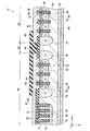
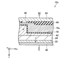
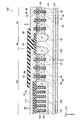
- FIG. 2 is a plan view showing a part of the semiconductor device according to the first embodiment. II-II sectional view of the semiconductor device shown in FIG.
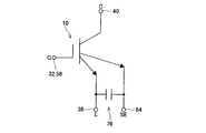
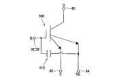
- FIG. 2 is a diagram showing a circuit equivalent to the semiconductor device shown in FIG. 1. Sectional drawing of the semiconductor device which concerns on the modification of 1st Example. Sectional drawing of the semiconductor device which concerns on the other modification of 1st Example. Sectional drawing of the semiconductor device which concerns on the other modification of 1st Example.
- FIG. 7 is a sectional view taken along line VII-VII in FIG. 6. Sectional drawing of the semiconductor device of 2nd Example.
- FIG. 9 illustrates a circuit equivalent to the semiconductor device illustrated in FIG. 8. Sectional drawing of the semiconductor device which concerns on the modification of 2nd Example.
- the semiconductor device disclosed in the present specification further includes a main electrode disposed on the main region of the upper surface of the semiconductor substrate, and a sense electrode disposed on the sense region of the upper surface of the semiconductor substrate. Also good. At least a part of the first region and the second region may be located below the sense electrode. According to such a configuration, the semiconductor substrate can be effectively used by forming a part of the first region and the second region below the sense electrode. As a result, an increase in size of the semiconductor device can be suppressed.
- the first region may be a semiconductor layer exposed on the upper surface of the semiconductor substrate.
- at least one trench extending downward from the upper surface of the semiconductor substrate may be formed in the first region.
- the second region may be a conductor disposed in the trench.
- the insulating film may be disposed between the wall surface of the trench and the second region. According to such a configuration, by disposing the conductor (second region) and the insulating film in the trench formed in the first region, the capacitance of the capacitor configured by the first region, the second region, and the insulating film. Can be increased efficiently.
- the element structure of the main region has a first conductivity type main drift region, a second conductivity type main body region in contact with the main drift region, and a main body region. And a first conductivity type main contact region separated from the main drift region by the main body region, and a main body region in a range separating the main contact region and the main drift region through the gate insulating film And a main gate electrode. Further, the element structure of the sense region is in contact with the first conductivity type sense drift region, the second conductivity type sense body region in contact with the sense drift region, and the sense body region.
- a main electrode that contacts the main contact region may be disposed on the main region of the upper surface of the semiconductor substrate.
- a sense electrode in contact with the sense contact region may be disposed on the sense region in the upper surface of the semiconductor substrate.
- switching elements are formed in the main region and the sense region, and the current flowing through the main region can be detected by the current flowing through the sense region.
- the first region may be electrically connected to the main electrode, and the second region may be electrically connected to the sense electrode.
- the sense electrode and the main electrode are connected by the capacitor. For this reason, even if electrostatic discharge occurs in the sense electrode, it is possible to suppress application of an overvoltage to the sense electrode. As a result, an overvoltage is suppressed from being applied to the gate insulating film that covers the sense gate electrode, and this gate insulating film can be protected.
- the first region may be electrically connected to the sense electrode, and the second region may be electrically connected to the main gate electrode or the sense gate electrode.
- the sense electrode and the sense gate electrode are connected by the capacitor. For this reason, even if electrostatic discharge occurs in the sense electrode, it is possible to suppress application of an overvoltage to the sense electrode. As a result, an overvoltage is suppressed from being applied to the gate insulating film that covers the sense gate electrode, and this gate insulating film can be protected.
- the semiconductor device 10 includes a semiconductor substrate 12, insulating films 36, 44, 46, 62 and electrodes 38, 64 formed on the upper surface of the semiconductor substrate 12, and a lower surface of the semiconductor substrate 12.
- the formed electrode 40 is provided.
- the semiconductor substrate 12 has a main region 20, a sense region 50, and an isolation region 80. That is, the main region 20 and the sense region 50 are formed on the same semiconductor substrate 12.
- the isolation region 80 is disposed between the main region 20 and the sense region 50. As apparent from FIG. 1, the sense region 50 is smaller than the main region 20.
- a known substrate for example, a silicon substrate (Si substrate), a silicon carbide substrate (SiC substrate), or the like
- a region where a main emitter electrode 38 (described later) is formed is referred to as a main region 20
- a region where a sense emitter electrode 64 (described later) is formed is referred to as a sense region 50.
- an emitter region 34 As shown in FIG. 2, an emitter region 34, a body region 26, a drift region 24, and a collector region 22 are formed in the main region 20 of the semiconductor substrate 12.
- the emitter region 34 is an n + type semiconductor region and is formed in a range facing the upper surface of the semiconductor substrate 12.
- a plurality of emitter regions 34 are formed at intervals in the x direction.
- Each emitter region 34 is formed in an island shape extending in the y direction.
- the body region 26 is a p ⁇ type semiconductor region and is formed below the emitter region 34.
- the body region 26 is in contact with the lower surface and the side surface of the emitter region 34.
- a part of the body region 26 is located between adjacent emitter regions 34 and exposed on the upper surface of the semiconductor substrate 12.
- the drift region 24 is an n ⁇ type semiconductor region and is formed below the body region 26.
- the drift region 24 is in contact with the lower surface of the body region 26.
- the drift region 24 is separated from the emitter region 34 by the body region 26.
- the drift region 24 is formed on the entire surface of the semiconductor substrate 12. Therefore, the drift region 24 is also formed in the sense region 50 and the isolation region 80.
- the collector region 22 is a p + type semiconductor region and is formed in a range facing the lower surface of the semiconductor substrate 12.
- the collector region 22 is in contact with the lower surface of the drift region 24.
- the collector region 22 is separated from the body region 26 by the drift region 24.
- the collector region 22 is formed on the entire surface of the semiconductor substrate 12. Therefore, the collector region 22 is also formed in the sense region 50 and the isolation region 80.
- a plurality of gate trenches 28 are formed in the main region 20 described above.
- the gate trenches 28 extend in the y direction and are arranged at intervals in the x direction.
- the gate trench 28 penetrates the emitter region 34 and the body region 26, and its lower end extends to the drift region 24.
- a gate electrode 32 is formed in the gate trench 28.
- the gate electrode 32 is formed so that the lower end thereof is slightly deeper than the lower surface of the body region 26.
- polysilicon or the like can be used as the material of the gate electrode 32.
- An insulating film 30 is filled between the wall surface of the gate trench 28 and the gate electrode 32. For this reason, the gate electrode 32 faces the body region 26 and the emitter region 24 with the insulating film 30 interposed therebetween.
- An insulating film 36 is formed on the gate electrode 32.
- the gate electrode 32 is insulated from the main emitter electrode 38 by the insulating film 36.
- a collector electrode 40 is formed on the lower surface of the semiconductor substrate 12.
- the collector electrode 40 is in ohmic contact with the collector region 22.
- the collector electrode 40 is formed on the entire surface of the semiconductor substrate 12. Therefore, the collector electrode 40 is formed not only in the main region 20 but also in the sense region 50 and the isolation region 80.
- a main emitter electrode 38 is formed on the upper surface of the semiconductor substrate 12.
- the main emitter electrode 38 is formed so as to cover the insulating film 36 and is insulated from the gate electrode 32.
- the main emitter electrode 38 is in ohmic contact with the emitter region 34 and the body region 26.
- the main emitter electrode 38 is formed on the main region 20 of the semiconductor substrate 12.
- a vertical IGBT Insulated Gate Bipolar Transistor
- the IGBT formed in the main region 20 is surrounded by the diffusion layer 42.
- the diffusion layer 42 is a p + type semiconductor region and is formed in a range facing the upper surface of the semiconductor substrate 12.
- the diffusion layer 42 is in contact with the body region 26 and the drift region 24 and surrounds the body region 26.
- the diffusion layer 42 is formed to a position deeper than the lower end of the gate trench 28.
- a part of the diffusion layer 42 is located in the main region 20 (below the main emitter electrode 38), and in the isolation region 80 and the sense region 50 (that is, below the sense emitter electrode 64). Is also located.
- An insulating film 44 is formed on the upper surface of the diffusion layer 42. This prevents the diffusion layer 42 from coming into direct contact with the main emitter electrode 38 and the sense emitter electrode 64.
- Sense region 50 An IGBT having the same structure as that of the main region 20 is also formed in the sense region 50. That is, an n + type emitter region 60, a p ⁇ type body region 52, an n ⁇ type drift region 24, and a p + type collector region 22 are formed in the sense region 50 of the semiconductor substrate 12. Yes. A plurality of gate trenches 54 are also formed in the sense region 50, and a gate electrode 58 and an insulating film 56 are formed in the gate trench 54. The emitter region 60, the body region 52, the drift region 24, the collector region 22, the gate electrode 58 and the insulating film 56 form an IGBT. As apparent from FIG. 1, the area of the IGBT formed in the sense region 50 is much smaller than the area of the IGBT formed in the main region 20.
- a collector electrode 40 is formed on the lower surface of the semiconductor substrate 12.
- a sense emitter electrode 64 is formed on the upper surface of the semiconductor substrate 12. The sense emitter electrode 64 is formed so as to cover the insulating films 62 and 44 and is insulated from the gate electrode 58. The sense emitter electrode 64 is in ohmic contact with the emitter region 60 and the body region 52.
- the IGBT formed in the sense region 50 is surrounded by the diffusion layer 76.
- the diffusion layer 76 is a p + type semiconductor region and is formed in a range facing the upper surface of the semiconductor substrate 12.
- the diffusion layer 76 is in contact with the body region 52 and the drift region 24 and is formed to a position deeper than the lower end of the gate trench 54 (that is, the gate trench 28 of the main region 20).
- the diffusion layer 76 surrounds the body region 52.
- the drift region 24 is disposed between the diffusion layer 76 and the diffusion layer 42, and the diffusion layer 76 is surrounded by the drift region 24. Thereby, the diffusion layer 76 is separated from the diffusion layer 42.
- An insulating film 44 is also formed on the upper surface of the diffusion layer 76.
- the insulating film 44 is also formed on the upper surface of the drift region 24 in a range that separates the diffusion layer 76 and the diffusion layer 42.
- a diffusion layer 42 is further formed in the sense region 50 of the semiconductor substrate 12. That is, the diffusion layer 42 surrounding the IGBT in the main region 20 is formed up to the lower side of the sense emitter electrode 64.
- a plurality of trenches 68 are formed in the diffusion layer 42.
- the plurality of trenches 68 are formed in the entire portion of the diffusion layer 42 located below the sense electrode 64. That is, the trench 68 extends from one end to the other end in the y direction of the sense electrode 64 (see FIG. 1), and one end in the x direction of the sense electrode from the boundary between the drift region 24 and the diffusion layer 42 (lower end in FIG. 1). Are arranged at intervals in the x direction.
- each trench 68 extends downward from the upper surface of the semiconductor substrate 12, and its lower end is located in the diffusion layer 42. That is, the lower end of the trench 68 does not reach the drift region 24.
- the depth of the trench 68 is the same as the depth of the gate trenches 54 and 28.
- a conductor 72 is formed in the trench 68.
- polysilicon or the like can be used as the material of the conductor 72.
- An insulating film 70 is filled between the wall surface of the trench 68 and the conductor 72. Therefore, the conductor 72 is opposed to the diffusion layer 42 with the insulating film 70 interposed therebetween.
- the upper end of the conductor 72 in each trench 68 is connected to the conductive layer 74.
- the conductive layer 74 is disposed in the insulating film 44.
- An opening is formed in the insulating film 44 at a position (not shown), and the conductive layer 74 and the sense emitter electrode 64 are connected through this opening.
- the isolation region 80 is a region that separates the main region 20 and the sense region 50 and is formed so as to surround the sense region 50.
- a diffusion layer 42, a drift region 24, and a diffusion layer 76 are formed in a range facing the upper surface of the semiconductor substrate 12 (see FIG. 2).
- An insulating film 44 and an insulating film 46 are formed on the upper surface of the drift region 24.
- the insulating film 46 is formed up to the main emitter electrode 38 and the sense emitter electrode 64.
- the collector region 22 is formed below the drift region 24.
- the gate electrodes 32 and 58 have an ON potential (a potential higher than the potential necessary for forming a channel). ) Is applied, the semiconductor device 10 is turned on. That is, by applying an ON potential to the gate electrodes 32 and 58, channels are formed in the body regions 26 and 52 in a range in contact with the insulating films 30 and 56. Then, in the main region 20, a current flows from the collector electrode 40 to the main emitter electrode 38, and in the sense region 50, a current flows from the collector electrode 40 to the sense emitter electrode 64.
- the ratio of the current flowing through the main region 20 and the current flowing through the sense region 50 is determined by the area ratio between the main region 20 and the sense region 50 and is a substantially constant value. Therefore, by detecting the current flowing through the sense region 50, the current value flowing through the main region 20 can be calculated from the detected current value and the sense ratio.
- the trench 68 is formed in the diffusion layer 42 of the sense region 50, and the conductor 72 and the insulating film 70 are disposed in the trench 68.
- the diffusion layer 42 is electrically connected to the main emitter electrode 38 via the body region 26, and the conductor 72 is electrically connected to the sense emitter electrode 64 via the conductive layer 74. That is, the same potential as that applied to the main emitter electrode 38 is applied to the diffusion layer 42, and the same potential as that applied to the sense emitter electrode 64 is applied to the conductor 72. Therefore, in the semiconductor device 10 of this embodiment, as shown in FIG.
- a capacitor 76 is constituted by the diffusion layer 42, the insulating film 70, and the conductor 72, and one end of the capacitor 76 is connected to the main emitter electrode 38. On the other hand, the other end of the capacitor 76 is connected to the sense emitter electrode 64. Therefore, even if electrostatic discharge occurs in the sense emitter electrode 64, the capacitor 76 between the sense emitter electrode 64 and the main emitter electrode 38 and the capacitor between the sense emitter electrode 64 and the gate electrode 58 (the gate electrode 58 and the insulating film) The electric charge is stored in a capacitor constituted by 56 and the body region 52. As a result, application of an excessive voltage to the insulating film 56 is suppressed, and the electrostatic resistance of the sense region 50 can be improved.
- the capacitor 76 is only formed between the sense emitter electrode 64 and the main emitter electrode 38, a current path for releasing charges due to electrostatic discharge is not required. For this reason, a leak current due to the current path does not occur, and it is not necessary to consider that the parasitic resistance of the current path is lowered to quickly release the charge.
- the capacitor 76 is formed on the semiconductor substrate 12 below the sense emitter electrode 64. Therefore, the formation of the capacitor 76 does not increase the size of the semiconductor substrate 12, and the size of the semiconductor device 10 does not increase.
- a trench 68 is formed in the entire sense emitter electrode 64 (excluding the region where the IGBT is formed), and the interval between the trenches 68 is also shorter than the interval between the gate trenches 28 and 54. Therefore, the capacitance of the capacitor 76 can be effectively increased, and the electrostatic resistance of the sense region 50 can be effectively increased.
- the conductive layer 74 in the insulating film 44, the conductive layer 74, the insulating film 44, and the diffusion layer 42 also constitute a capacitor. This also increases the capacitance component of the sense region 50 and increases the electrostatic resistance.
- the diffusion layer 42 in the sense region 50 is separated from the body region 52 by the drift region 24 and the diffusion layer 76. For this reason, the holes from the collector electrode 40 are suppressed from flowing to the sense emitter electrode 64 through the diffusion layer 42. For this reason, the accuracy of the sense current flowing through the sense region 50 (the accuracy of the sense ratio) is improved, and the current flowing through the main region 20 can be detected with high accuracy.
- the conductive layer 74 is electrically connected to the sense emitter electrode 64 in the opening formed in the insulating film 44.
- the structure for electrically connecting the conductive layer and the sense emitter electrode is not limited to such a form.
- the upper surface of the conductive layer 74a connected to the conductor 72 is not covered with the insulating film 44a, and the entire upper surface of the conductive layer 74a is in contact with the sense emitter electrode 64a. You may do it.
- the conductor 72 can be electrically connected to the sense emitter electrode 64a, and the same effect as the first embodiment can be obtained.
- portions having the same configuration as those of the semiconductor device 10 shown in FIGS. Similarly, in the semiconductor device of FIGS. 5 to 7, the same reference numerals are given to the parts having the same configuration as the semiconductor device 10 shown in FIGS. 1 and 2.
- the p + -type diffusion layer 42 is formed below the sense emitter electrode 64, and the trench 68 and the like are formed in the diffusion layer 42.
- a p ⁇ -type diffusion region 78 may be formed below the sense emitter electrode 64 as in the semiconductor device 10b shown in FIG.
- the diffusion region 78 is in contact with the diffusion region 42 and is electrically connected to the main emitter electrode 38 via the diffusion region 42 and the body region 26. Even with such a configuration, the same operational effects as the semiconductor device 10 of the first embodiment can be obtained. If the depth and concentration of the diffusion region 78 are the same as those of the body regions 26 and 52, the body regions 26 and 52 and the diffusion region 78 can be formed by the same process. Further, when the diffusion region 78 has the same depth as the body regions 26 and 52, the trench 68 penetrates the diffusion region 78 and the lower end thereof reaches the drift region 24.
- the conductor 72 protrudes upward from the trench 68 and is connected to the conductive film 74 in the insulating film 44.
- the conductor 72 a may be disposed only in the trench 68 as with the gate electrodes 32 and 58.
- an opening 45 is formed in the insulating film 44 at the end in the longitudinal direction of the conductor 72a, and the conductor 72a and the sense emitter electrode 64 are electrically connected through the opening 45. May be. Even with such a configuration, the same operational effects as the semiconductor device 10 of the first embodiment can be obtained.
- the gate electrodes 32 and 58 and the conductor 72a can be formed by the same process.
- the semiconductor device 100 of the second embodiment is different in that a capacitor is formed between the sense emitter electrode 64 and the gate electrodes 32 and 58.
- the description thereof is omitted.
- symbol is attached
- the body region 52 and the p + type diffusion layer 102 are in contact with each other, and the diffusion layer 102 is electrically connected to the sense emitter electrode 64 through the body region 52. ing.
- the same potential as that of the sense emitter electrode 64 is applied to the diffusion layer 102.
- the diffusion layer 102 surrounds the body region 52, and the diffusion layer 102 and the diffusion layer 42 are separated by the drift region 24. For this reason, the diffusion layer 102 is not electrically connected to the main emitter electrode 38 via the diffusion layer 42 and the body region 26.
- the diffusion layer 102 is formed in a range facing the upper surface of the semiconductor substrate 12, and is formed up to a position deeper than the lower end of the gate trench 54.
- the diffusion layer 102 is formed on the entire area below the sense emitter electrode 64. That is, when viewed in plan, the diffusion layer 102 is formed over the entire sense emitter electrode 64.
- a plurality of trenches 104 are formed in the diffusion layer 102.
- the plurality of trenches 104 are formed in the entire diffusion layer 102.
- the plurality of trenches 104 extend in the y direction and are arranged at intervals in the x direction.
- the trench 104 is formed in the same manner as the trench 68 of the first embodiment, and a conductor 108 and an insulating film 106 are formed therein. For this reason, the conductor 108 faces the diffusion layer 102 with the insulating film 106 interposed therebetween.
- the upper end of the conductor 108 in each trench 104 is connected to the conductive layer 110.
- the conductive layer 110 is disposed in the insulating film 44. An opening is formed in the insulating film 44 at a position not shown, and the conductive layer 110 is electrically connected to a gate wiring (not shown) through this opening. For this reason, the conductor 108 is electrically connected to the gate wiring through the conductive layer 110, and the same potential as that of the gate electrodes 32 and 58 is applied.
- the trench 104 is formed in the diffusion layer 102 of the sense region 120, and the conductor 108 and the insulating film 106 are disposed in the trench 104.
- the diffusion layer 102 is electrically connected to the sense emitter electrode 64 via the body region 52, and the conductor 108 is electrically connected to the gate electrodes 32 and 58 via the conductive layer 110. That is, the same potential as that applied to the sense emitter electrode 64 is applied to the diffusion layer 102, and the same potential as that applied to the gate electrodes 32 and 58 is applied to the conductor 108. Therefore, in the semiconductor device 100 of this embodiment, as shown in FIG.
- a capacitor 112 is constituted by the diffusion layer 102, the insulating film 106, and the conductor 108, and one end of the capacitor 112 is connected to the sense emitter electrode 64.
- the other end of the capacitor 112 is connected to the gate electrodes 32 and 58. Therefore, even if electrostatic discharge occurs in the sense emitter electrode 64, the capacitor 112 between the sense emitter electrode 64 and the gate electrodes 32 and 58 and the capacitor between the sense emitter electrode 64 and the gate electrode 58 (insulated from the gate electrode 58) Charge is stored in a capacitor formed by the film 56 and the body region 52. As a result, application of an excessive voltage to the insulating film 56 is suppressed, and the electrostatic resistance of the sense region 50 can be improved.
- the configuration of the trench 104, the insulating film 106, and the conductor 108 can be made substantially the same as the configuration of the gate trench 54, the insulating film 56, and the gate electrode 58. Therefore, these can be formed by the same process, and the semiconductor device 100 can be easily manufactured.
- the diffusion layer 102 is brought into contact with the body region 52, and the trench 104, the conductor 108, and the insulating film 106 are formed in the diffusion layer 102.
- the configuration of the capacitor 112 formed in the sense region 120 is not limited to such a configuration.
- the diffusion layer in which the trench 104, the conductor 108 and the insulating film 106 are formed may be separated from the body region 52 by the drift region 24.
- an opening may be formed in the insulating film formed on the upper surface of the diffusion layer, and the diffusion layer and the sense emitter electrode 64 may be electrically connected via the opening.
- the conductor 108 disposed in the trench 104 may be configured to bury the conductor 108 in the trench 104 as in the semiconductor device 10c shown in FIG.
- the trench 104 is formed in the body region 52a of the sense region 120a separately from the gate trench 54, and the conductor 108 and the insulating film 106 are formed in the trench 104. It may be. Even with such a configuration, the capacitor component of the sense region 120a can be increased, and the electrostatic resistance can be improved.
- the upper ends of the two trenches 104a adjacent to the gate trench 54 functioning as the IGBT are closed with the insulating film 44c, and the insulating film 44c includes the adjacent trench 104a. No opening is formed between them. As a result, the holes are suppressed from flowing to the sense emitter electrode 64b through other than the element portion, and the accuracy of the sense current (the accuracy of the sense ratio) is improved.
- capacitors are formed in the sense regions 50, 120, but a capacitor (trench, conductor, insulating film) may be formed in the main region 20. . Even with such a configuration, the capacitance components of the sense regions 50 and 120 can be increased, and the electrostatic resistance can be improved.
- a vertical semiconductor element (specifically, an IGBT) is formed on the semiconductor substrate 12, but a horizontal semiconductor element may be formed on the semiconductor substrate 12.
- the semiconductor element formed on the semiconductor substrate 12 is not limited to the IGBT, and may be another semiconductor element (for example, MOS).
Landscapes
- Metal-Oxide And Bipolar Metal-Oxide Semiconductor Integrated Circuits (AREA)
Abstract
半導体装置は、メイン領域と、メイン領域に流れる電流を検知するためのセンス領域とを備える半導体基板を有している。半導体基板のメイン領域とセンス領域は、同一の素子構造を有している。半導体基板のセンス領域は、さらに、半導体装置の第1の部位と電気的に接続される導電性の第1領域と、半導体装置の第1の部位とは異なる第2の部位と電気的に接続される導電性の第2領域と、第1領域と第2領域との間に配置され、第1領域から第2領域を隔離する絶縁膜とを有している。
Description
本明細書に開示の技術は、同一の半導体基板にメイン領域とセンス領域とが形成された半導体装置に関する。
半導体装置に過電流が流れることを防止するために、半導体装置を流れる電流を検知するためのセンス領域が設けられた半導体装置が開発されている。日本国特許公開公報平10-326897号には、同一の半導体基板にメイン領域とセンス領域とが形成された半導体装置が開示されている。この半導体装置では、メイン領域とセンス領域にIGBTが作り込まれている。この半導体装置では、センス領域を流れる電流を検知することで、メイン領域を流れる電流を検知することができる。
この種の半導体装置では、メイン領域と比較してセンス領域の面積が極めて小さい。このため、センス領域の静電耐量はメイン領域の静電耐量より小さく、半導体装置の静電耐量は、センス領域の静電耐量で決まることとなる。その結果、センス領域を備えていない半導体装置と比較して、半導体装置の静電耐量が低くなる。
本明細書は、同一の半導体基板にメイン領域とセンス領域とが形成された半導体装置において、半導体装置の静電耐量を向上することができる技術を開示する。
本明細書が開示する半導体装置は、メイン領域と、メイン領域に流れる電流を検知するためのセンス領域とを備える半導体基板を有している。半導体基板のメイン領域とセンス領域のそれぞれは、同一の素子構造を有している。半導体基板のセンス領域は、前記素子構造に加えてさらに、導電性の第1領域と、導電性の第2領域と、絶縁膜を有している。第1領域は、半導体装置の第1の部位と電気的に接続されている。第2領域は、半導体装置の第1の部位とは異なる第2の部位と電気的に接続されている。絶縁膜は、第1領域と第2領域との間に配置され、第1領域から第2領域を隔離する。
この半導体装置では、導電性の第1領域と、導電性の第2領域と、絶縁膜とがセンス領域に形成され、これらによってキャパシタが構成されている。第1領域と第2領域とは半導体装置の異なる部位と電気的に接続されており、異なる電位が印加可能となっている。このため、第1領域と第2領域に異なる電位が印加されると、第1領域と第2領域と絶縁膜によって構成されるキャパシタに電荷が蓄えられる。したがって、センス領域の容量を増大することが可能となり、半導体装置の静電耐量を向上することができ得る。
本明細書に開示する半導体装置では、半導体基板の上面のうちメイン領域上に配置されるメイン電極と、半導体基板の上面のうちセンス領域上に配置されるセンス電極と、をさらに有していてもよい。第1領域及び第2領域の少なくとも一部は、センス電極の下方に位置していてもよい。このような構成によると、センス電極の下方に第1領域及び第2領域の一部を形成することで、半導体基板を有効に活用することができる。これによって、半導体装置が大型化することを抑制することができる。
本明細書に開示する半導体装置では、第1領域は、半導体基板の上面に露出している半導体層としてもよい。この場合、第1領域には、半導体基板の上面から下方に伸びる少なくとも1つのトレンチが形成されていてもよい。第2領域は、トレンチ内に配置されている導電体としてもよい。絶縁膜は、トレンチの壁面と第2領域の間に配置されていてもよい。このような構成によると、第1領域に形成されたトレンチ内に導電体(第2領域)と絶縁膜を配置することで、第1領域と第2領域と絶縁膜で構成されるキャパシタの容量を効率的に増大することができる。
本明細書に開示する半導体装置では、メイン領域の素子構造は、第1導電型のメインドリフト領域と、メインドリフト領域と接している第2導電型のメインボディ領域と、メインボディ領域と接しており、メインボディ領域によってメインドリフト領域と分離されている第1導電型のメインコンタクト領域と、メインコンタクト領域とメインドリフト領域とを分離している範囲のメインボディ領域とゲート絶縁膜を介して対向しているメインゲート電極と、を有していてもよい。また、センス領域の素子構造は、第1導電型のセンスドリフト領域と、センスドリフト領域と接している第2導電型のセンスボディ領域と、センスボディ領域と接しており、センスボディ領域によってセンスドリフト領域と分離されている第1導電型のセンスコンタクト領域と、センスコンタクト領域とセンスドリフト領域とを分離している範囲のセンスボディ領域とゲート絶縁膜を介して対向しているセンスゲート電極と、を有していてもよい。半導体基板の上面のうちメイン領域上には、メインコンタクト領域と接触するメイン電極が配置されていてもよい。半導体基板の上面のうちセンス領域上には、センスコンタクト領域と接するセンス電極が配置されていてもよい。この半導体装置では、メイン領域とセンス領域にスイッチング素子が形成され、センス領域を流れる電流によってメイン領域を流れる電流を検知することができる。
上記の半導体装置では、第1領域がメイン電極と電気的に接続され、第2領域がセンス電極と電気的に接続されていてもよい。このような構成によると、センス電極とメイン電極とがキャパシタにより接続される。このため、センス電極に静電気放電が生じたとしても、センス電極に過電圧が印加されることを抑制することができる。その結果、センスゲート電極を被覆するゲート絶縁膜に過電圧が印加されることが抑制され、このゲート絶縁膜を保護することができる。
あるいは、上記の半導体装置では、第1領域がセンス電極と電気的に接続され、第2領域がメインゲート電極又はセンスゲート電極と電気的に接続されていてもよい。このような構成によると、センス電極とセンスゲート電極とがキャパシタにより接続される。このため、センス電極に静電気放電が生じたとしても、センス電極に過電圧が印加されることを抑制することができる。その結果、センスゲート電極を被覆するゲート絶縁膜に過電圧が印加されることが抑制され、このゲート絶縁膜を保護することができる。
(第1実施例) 以下、第1実施例の半導体装置10について、図面を参照して説明する。図1,2に示すように、半導体装置10は、半導体基板12と、半導体基板12の上面に形成された絶縁膜36,44,46,62及び電極38,64と、半導体基板12の下面に形成された電極40を備えている。半導体基板12は、メイン領域20とセンス領域50と分離領域80を有している。すなわち、メイン領域20とセンス領域50は、同一の半導体基板12に形成されている。分離領域80は、メイン領域20とセンス領域50との間に配置されている。図1から明らかなように、センス領域50は、メイン領域20と比較して小さい。なお、半導体基板12には、公知の基板(例えば、シリコン基板(Si基板),炭化シリコン基板(SiC基板)等)を用いることができる。また、本明細書では、メインエミッタ電極38(後述)が形成されている領域をメイン領域20といい、センスエミッタ電極64(後述)が形成されている領域をセンス領域50という。
(メイン領域20)
まず、メイン領域20について説明する。図2に示すように、半導体基板12のメイン領域20には、エミッタ領域34と、ボディ領域26と、ドリフト領域24と、コレクタ領域22が形成されている。エミッタ領域34は、n+型の半導体領域であり、半導体基板12の上面に臨む範囲に形成されている。エミッタ領域34は、x方向に間隔を空けて複数形成されている。各エミッタ領域34は、y方向に伸びる島状に形成されている。
まず、メイン領域20について説明する。図2に示すように、半導体基板12のメイン領域20には、エミッタ領域34と、ボディ領域26と、ドリフト領域24と、コレクタ領域22が形成されている。エミッタ領域34は、n+型の半導体領域であり、半導体基板12の上面に臨む範囲に形成されている。エミッタ領域34は、x方向に間隔を空けて複数形成されている。各エミッタ領域34は、y方向に伸びる島状に形成されている。
ボディ領域26は、p-型の半導体領域であり、エミッタ領域34の下方に形成されている。ボディ領域26は、エミッタ領域34の下面及び側面に接している。ボディ領域26の一部は、隣接するエミッタ領域34の間に位置し、半導体基板12の上面に露出している。
ドリフト領域24は、n-型の半導体領域であり、ボディ領域26の下方に形成されている。ドリフト領域24は、ボディ領域26の下面に接している。ドリフト領域24は、ボディ領域26によってエミッタ領域34から分離されている。ドリフト領域24は、半導体基板12の全面に形成されている。したがって、ドリフト領域24は、センス領域50及び分離領域80にも形成されている。
コレクタ領域22は、p+型の半導体領域であり、半導体基板12の下面に臨む範囲に形成されている。コレクタ領域22は、ドリフト領域24の下面に接している。コレクタ領域22は、ドリフト領域24によってボディ領域26から分離されている。コレクタ領域22は、半導体基板12の全面に形成されている。したがって、コレクタ領域22は、センス領域50及び分離領域80にも形成されている。
上述したメイン領域20には、複数のゲートトレンチ28が形成されている。ゲートトレンチ28は、y方向に伸びており、x方向に間隔を空けて配列されている。ゲートトレンチ28は、エミッタ領域34及びボディ領域26を貫通し、その下端がドリフト領域24まで伸びている。ゲートトレンチ28内には、ゲート電極32が形成されている。ゲート電極32は、その下端がボディ領域26の下面よりわずかに深くなるように形成されている。ゲート電極32の材料には、例えば、ポリシリコン等を用いることができる。ゲートトレンチ28の壁面とゲート電極32の間には絶縁膜30が充填されている。このため、ゲート電極32は、絶縁膜30を介してボディ領域26及びエミッタ領域24に対向している。ゲート電極32の上部には絶縁膜36が形成されている。絶縁膜36によって、ゲート電極32は、メインエミッタ電極38から絶縁されている。
半導体基板12の下面には、コレクタ電極40が形成されている。コレクタ電極40は、コレクタ領域22とオーミック接触している。コレクタ電極40は、半導体基板12の全面に形成されている。したがって、コレクタ電極40は、メイン領域20だけではなく、センス領域50及び分離領域80にも形成されている。
半導体基板12の上面には、メインエミッタ電極38が形成されている。メインエミッタ電極38は、絶縁膜36を覆うように形成されており、ゲート電極32から絶縁されている。メインエミッタ電極38は、エミッタ領域34、ボディ領域26とオーミック接触している。メインエミッタ電極38は、半導体基板12のメイン領域20上に形成されている。
上述したことから明らかなように、半導体基板12のメイン領域20には縦型のIGBT(Insulated Gate Bipolar Transistor)が形成されている。メイン領域20に形成されたIGBTは、拡散層42によって囲まれている。拡散層42は、p+型の半導体領域であり、半導体基板12の上面に臨む範囲に形成されている。拡散層42は、ボディ領域26及びドリフト領域24と接しており、ボディ領域26の周囲を取囲んでいる。拡散層42は、ゲートトレンチ28の下端よりも深い位置まで形成されている。図1に示すように、拡散層42は、その一部がメイン領域20(メインエミッタ電極38の下方)に位置すると共に、分離領域80及びセンス領域50(すなわち、センスエミッタ電極64の下方)にも位置している。なお、拡散層42の上面には絶縁膜44が形成されている。これにより、拡散層42がメインエミッタ電極38及びセンスエミッタ電極64と直接接触することが防止されている。
(センス領域50)
次に、センス領域50について説明する。センス領域50にも、メイン領域20と同一構造のIGBTが形成されている。すなわち、半導体基板12のセンス領域50には、n+型のエミッタ領域60と、p-型のボディ領域52と、n-型のドリフト領域24と、p+型のコレクタ領域22が形成されている。また、センス領域50にも複数のゲートトレンチ54が形成され、ゲートトレンチ54内にはゲート電極58及び絶縁膜56が形成されている。エミッタ領域60、ボディ領域52、ドリフト領域24、コレクタ領域22、ゲート電極58及び絶縁膜56によってIGBTが形成されている。図1から明らかなように、センス領域50に形成されるIGBTの面積は、メイン領域20に形成されるIGBTの面積よりも格段に小さい。
次に、センス領域50について説明する。センス領域50にも、メイン領域20と同一構造のIGBTが形成されている。すなわち、半導体基板12のセンス領域50には、n+型のエミッタ領域60と、p-型のボディ領域52と、n-型のドリフト領域24と、p+型のコレクタ領域22が形成されている。また、センス領域50にも複数のゲートトレンチ54が形成され、ゲートトレンチ54内にはゲート電極58及び絶縁膜56が形成されている。エミッタ領域60、ボディ領域52、ドリフト領域24、コレクタ領域22、ゲート電極58及び絶縁膜56によってIGBTが形成されている。図1から明らかなように、センス領域50に形成されるIGBTの面積は、メイン領域20に形成されるIGBTの面積よりも格段に小さい。
センス領域50においても、半導体基板12の下面にはコレクタ電極40が形成されている。一方、センス領域50においては、半導体基板12の上面にセンスエミッタ電極64が形成されている。センスエミッタ電極64は、絶縁膜62,44を覆うように形成されており、ゲート電極58から絶縁されている。センスエミッタ電極64は、エミッタ領域60及びボディ領域52とオーミック接触している。
センス領域50に形成されたIGBTは、拡散層76によって囲まれている。拡散層76は、p+型の半導体領域であり、半導体基板12の上面に臨む範囲に形成されている。拡散層76は、ボディ領域52及びドリフト領域24と接しており、ゲートトレンチ54(すなわち、メイン領域20のゲートトレンチ28)の下端よりも深い位置まで形成されている。図1に示すように、拡散層76は、ボディ領域52を取囲んでいる。拡散層76と拡散層42の間にはドリフト領域24が配置されており、拡散層76はドリフト領域24によって囲まれている。これによって、拡散層76は、拡散層42から分離されている。拡散層76の上面にも絶縁膜44が形成されている。絶縁膜44は、拡散層76と拡散層42を分離する範囲のドリフト領域24の上面にも形成されている。
半導体基板12のセンス領域50には、さらに拡散層42が形成されている。すなわち、メイン領域20のIGBTを取囲む拡散層42は、センスエミッタ電極64の下方にまで形成されている。図2から明らかなように、センス領域50においては、拡散層42に複数のトレンチ68が形成されている。複数のトレンチ68は、拡散層42のうち、センス電極64の下方に位置する部分の全体に形成されている。すなわち、トレンチ68は、センス電極64のy方向の一端から他端まで伸び(図1参照)、また、ドリフト領域24と拡散層42の境界からセンス電極のx方向の一端(図1の下端)までの全体に、x方向に間隔を空けて配列されている。なお、隣り合うトレンチ68の間隔は、ゲートトレンチ54,28の間隔よりも狭くされている。各トレンチ68は、半導体基板12の上面から下方に伸び、その下端は拡散層42内に位置している。すなわち、トレンチ68の下端はドリフト領域24にまで達していない。トレンチ68の深さは、ゲートトレンチ54,28の深さと同一となっている。トレンチ68内には導電体72が形成されている。導電体72の材料には、例えば、ポリシリコン等を用いることができる。トレンチ68の壁面と導電体72の間には絶縁膜70が充填されている。このため、導電体72は、絶縁膜70を介して拡散層42に対向している。
各トレンチ68内の導電体72の上端は、導電層74に接続されている。導電層74は、絶縁膜44内に配置されている。絶縁膜44には、図示しない位置で開口が形成されており、この開口を介して導電層74とセンスエミッタ電極64とが接続されている。
(分離領域80)
次に、分離領域80について説明する。図1に示すように、分離領域80は、メイン領域20とセンス領域50とを分離する領域であり、センス領域50を取囲むように形成されている。図2に示すように、分離領域80において、半導体基板12の上面に臨む範囲には、拡散層42とドリフト領域24と拡散層76が形成されている(図2参照)。ドリフト領域24の上面には、絶縁膜44及び絶縁膜46が形成されている。絶縁膜46は、メインエミッタ電極38及びセンスエミッタ電極64上まで形成されている。なお、分離領域80においても、ドリフト領域24の下方にはコレクタ領域22が形成されている。
次に、分離領域80について説明する。図1に示すように、分離領域80は、メイン領域20とセンス領域50とを分離する領域であり、センス領域50を取囲むように形成されている。図2に示すように、分離領域80において、半導体基板12の上面に臨む範囲には、拡散層42とドリフト領域24と拡散層76が形成されている(図2参照)。ドリフト領域24の上面には、絶縁膜44及び絶縁膜46が形成されている。絶縁膜46は、メインエミッタ電極38及びセンスエミッタ電極64上まで形成されている。なお、分離領域80においても、ドリフト領域24の下方にはコレクタ領域22が形成されている。
次に、半導体装置10の動作について説明する。メインエミッタ電極38及びセンスエミッタ電極64をグランド電位に接続し、コレクタ電極12を電源電位に接続した状態で、ゲート電極32,58にオン電位(チャネルが形成されるのに必要な電位以上の電位)を印加すると、半導体装置10がオンする。すなわち、ゲート電極32,58へのオン電位の印加により、絶縁膜30,56に接する範囲のボディ領域26、52にチャネルが形成される。すると、メイン領域20では、コレクタ電極40からメインエミッタ電極38に電流が流れ、センス領域50では、コレクタ電極40からセンスエミッタ電極64に電流が流れる。ここで、メイン領域20を流れる電流と、センス領域50を流れる電流の比(いわゆるセンス比)は、メイン領域20とセンス領域50の面積比で決まり、略一定の値となる。このため、センス領域50に流れる電流を検知することで、その検知した電流値とセンス比からメイン領域20を流れる電流値を算出することができる。
また、本実施例の半導体装置10では、センス領域50の拡散層42にトレンチ68が形成され、そのトレンチ68内に導電体72及び絶縁膜70が配置されている。そして、拡散層42は、ボディ領域26を介してメインエミッタ電極38に電気的に接続され、また、導電体72は、導電層74を介してセンスエミッタ電極64に電気的に接続されている。すなわち、拡散層42には、メインエミッタ電極38に印加される電位と同一の電位が印加され、導電体72には、センスエミッタ電極64に印加される電位と同一の電位が印加される。したがって、本実施例の半導体装置10では、図3に示すように、拡散層42と絶縁膜70と導電体72によってキャパシタ76が構成され、このキャパシタ76の一端がメインエミッタ電極38に接続される一方、キャパシタ76の他端がセンスエミッタ電極64に接続されていることとなる。したがって、センスエミッタ電極64に静電気放電が生じたとしても、センスエミッタ電極64とメインエミッタ電極38の間のキャパシタ76と、センスエミッタ電極64とゲート電極58の間のキャパシタ(ゲート電極58と絶縁膜56とボディ領域52によって構成されるキャパシタ)に電荷が蓄えられる。その結果、絶縁膜56に過大な電圧が印加されることが抑制され、センス領域50の静電耐量を向上することができる。
また、本実施例の半導体装置10では、センスエミッタ電極64とメインエミッタ電極38の間にキャパシタ76を形成するだけであるため、静電気放電による電荷を逃がすための電流経路を必要としない。このため、電流経路に起因するリーク電流が発生することはなく、また、電流経路の寄生抵抗を下げて電荷を速やかに逃すことを考慮する必要もない。
また、本実施例の半導体装置10では、キャパシタ76はセンスエミッタ電極64の下方の半導体基板12に形成される。したがって、キャパシタ76を形成することによって半導体基板12が大型化することはなく、半導体装置10が大型化することはない。また、センスエミッタ電極64の全体(IGBTが形成された領域を除く)にトレンチ68が形成され、トレンチ68の間隔もゲートトレンチ28,54の間隔よりも短くされている。したがって、キャパシタ76の容量を効果的に増大することができ、センス領域50の静電耐量を効果的に増大することができる。さらに、絶縁膜44内に導電層74を配置することで、導電層74と絶縁膜44と拡散層42によってもキャパシタが構成される。これによっても、センス領域50の容量成分を増大し、静電耐量の増大が図られている。
また、本実施例の半導体装置10では、センス領域50内の拡散層42は、ドリフト領域24及び拡散層76によって、ボディ領域52から分離されている。このため、コレクタ電極40からのホールが拡散層42を介してセンスエミッタ電極64に流れることが抑制される。このため、センス領域50を流れるセンス電流の精度(センス比の精度)が向上し、メイン領域20を流れる電流を精度よく検出することができる。
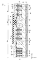
なお、上述した第1実施例の半導体装置10では、導電層74が絶縁膜44に形成された開口においてセンスエミッタ電極64と電気的に接続されていた。しかしながら、導電層とセンスエミッタ電極とを電気的に接続する構造は、このような形態に限られない。例えば、図4に示す半導体装置10aのように、導電体72に接続された導電層74aの上面が絶縁膜44aに覆われておらず、導電層74aの上面の全体がセンスエミッタ電極64aに接触していてもよい。このような構成によっても、導電体72をセンスエミッタ電極64aに電気的に接続することができ、第1実施例と同様の作用効果を奏することができる。なお、図4に示す半導体装置10aにおいて、図1,2に示す半導体装置10と同一の構成を備える部分については同一の符号を付している。(図5~7の半導体装置においても同様に、図1,2に示す半導体装置10と同一の構成を備える部分については同一の符号を付している。)
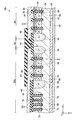
また、上述した第1実施例の半導体装置10では、センスエミッタ電極64の下方にp+型の拡散層42を形成し、その拡散層42にトレンチ68等を形成した。しかしながら、図5に示す半導体装置10bのように、センスエミッタ電極64の下方にp-型の拡散領域78を形成してもよい。この場合、拡散領域78は、拡散領域42と接触し、拡散領域42及びボディ領域26を介してメインエミッタ電極38と電気的に接続される。このような構成によっても、第1実施例の半導体装置10と同様の作用効果を奏することができる。なお、拡散領域78の深さ及び濃度がボディ領域26,52のそれらと同一とすると、ボディ領域26,52と拡散領域78を同一のプロセスで形成することができる。また、拡散領域78がボディ領域26,52と同一の深さとなると、トレンチ68は、拡散領域78を貫通し、その下端がドリフト領域24に達することとなる。
また、上述した第1実施例の半導体装置10では、導電体72がトレンチ68内から上方に突出し、絶縁膜44内で導電膜74に接続していた。しかしながら、図6に示す半導体装置10cのように、ゲート電極32,58と同様、導電体72aはトレンチ68内にのみ配置されていてもよい。この場合、図7に示すように、導電体72aの長手方向の端部において絶縁膜44に開口45を形成し、その開口45を介して導電体72aとセンスエミッタ電極64とを電気的に接続してもよい。このような構成によっても、第1実施例の半導体装置10と同様の作用効果を奏することができる。なお、ゲート電極32,58と導電体72aとは同一のプロセスで形成することができる。
(第2実施例) 第2実施例の半導体装置100では、第1実施例の半導体装置10と異なり、センスエミッタ電極64とゲート電極32,58との間にキャパシタが形成される点で異なる。ただし、その他の構成については、第1実施例の半導体装置10と同様の構成を備えるため、その説明を省略する。なお、第1実施例の半導体装置10と同様の構成となる部位には、同一の符号が付されている。
図8に示す半導体装置100では、センス領域120において、ボディ領域52とp+型の拡散層102とが接触し、拡散層102がボディ領域52を介してセンスエミッタ電極64と電気的に接続されている。これによって、拡散層102にセンスエミッタ電極64と同一の電位が印加される。また、拡散層102は、ボディ領域52の周囲を取り囲んでおり、拡散層102と拡散層42とはドリフト領域24で分離されている。このため、拡散層102が拡散層42及びボディ領域26を介してメインエミッタ電極38と電気的に接続されることはない。
拡散層102は、半導体基板12の上面に臨む範囲に形成されており、ゲートトレンチ54の下端よりも深い位置まで形成されている。拡散層102は、センスエミッタ電極64の下方の全体に形成されている。すなわち、平面視したときに、拡散層102は、センスエミッタ電極64の全体に形成されている。拡散層102には、複数のトレンチ104が形成されている。複数のトレンチ104は、拡散層102の全体に形成されている。複数のトレンチ104は、y方向に伸び、x方向に間隔を空けて配列されている。トレンチ104は、第1実施例のトレンチ68と同様に形成されており、その内部に導電体108と絶縁膜106が形成されている。このため、導電体108は、絶縁膜106を介して拡散層102に対向している。
各トレンチ104内の導電体108の上端は、導電層110に接続されている。導電層110は、絶縁膜44内に配置されている。絶縁膜44には、図示しない位置で開口が形成されており、この開口を介して導電層110がゲート配線(図示しない)と電気的に接続されている。このため、導電体108は、導電層110を介してゲート配線と電気的に接続されており、ゲート電極32,58と同一の電位が印加されるようになっている。
本実施例の半導体装置100では、センス領域120の拡散層102にトレンチ104が形成され、そのトレンチ104内に導電体108及び絶縁膜106が配される。そして、拡散層102は、ボディ領域52を介してセンスエミッタ電極64に電気的に接続され、導電体108は、導電層110を介してゲート電極32,58に電気的に接続されている。すなわち、拡散層102には、センスエミッタ電極64に印加される電位と同一の電位が印加され、導電体108には、ゲート電極32,58に印加される電位と同一の電位が印加される。したがって、本実施例の半導体装置100では、図9に示すように、拡散層102と絶縁膜106と導電体108によってキャパシタ112が構成され、このキャパシタ112の一端がセンスエミッタ電極64に接続される一方、キャパシタ112の他端がゲート電極32,58に接続されていることとなる。したがって、センスエミッタ電極64に静電気放電が生じたとしても、センスエミッタ電極64とゲート電極32,58の間のキャパシタ112と、センスエミッタ電極64とゲート電極58の間のキャパシタ(ゲート電極58と絶縁膜56とボディ領域52によって構成されるキャパシタ)に電荷が蓄えられる。その結果、絶縁膜56に過大な電圧が印加されることが抑制され、センス領域50の静電耐量を向上することができる。
また、半導体装置100では、トレンチ104と絶縁膜106と導電体108の構成を、ゲートトレンチ54と絶縁膜56とゲート電極58の構成と略同一とすることができる。このため、これらを同一のプロセスで形成することができ、半導体装置100を容易に製造することができる。
なお、上述した第2実施例では、拡散層102をボディ領域52と接触させ、この拡散層102にトレンチ104、導電体108及び絶縁膜106を形成した。しかしながら、センス領域120に形成されるキャパシタ112の構成は、このような構成に限られない。例えば、図1に示す第1実施例の半導体装置10のように、トレンチ104、導電体108及び絶縁膜106が形成される拡散層をドリフト領域24によってボディ領域52から分離してもよい。なお、このような構成を採る場合、拡散層の上面に形成された絶縁膜に開口を形成し、開口を介してこの拡散層とセンスエミッタ電極64とを電気的に接続すればよい。
また、トレンチ104内に配置される導電体108は、図6に示す半導体装置10cのように、トレンチ104内に導電体108を埋め込むような構成としてもよい。さらには、図10に示す半導体装置100aのように、センス領域120aのボディ領域52aにゲートトレンチ54とは別にトレンチ104を形成し、このトレンチ104内に導電体108及び絶縁膜106を形成するようにしてもよい。このような構成によっても、センス領域120aのキャパシタ成分を増大することができ、静電耐量を向上することができる。なお、半導体装置100aでは、IGBTとして機能するゲートトレンチ54(エミッタ領域60と接するゲートトレンチ)に隣接する2つのトレンチ104aの上端を絶縁膜44cで塞ぎ、この絶縁膜44cには、隣接するトレンチ104aの間に開口が形成されていない。これによって、ホールが素子部以外を通ってセンスエミッタ電極64bに流れることが抑制され、センス電流の精度(センス比の精度)の向上が図られている。
以上、本発明の実施例について詳細に説明したが、これらは例示に過ぎず、特許請求の範囲を限定するものではない。特許請求の範囲に記載の技術には、以上に例示した具体例を様々に変形、変更したものが含まれる。
例えば、上述した各実施例では、センス領域50,120にキャパシタ(トレンチ、導電体、絶縁膜)を形成したが、メイン領域20にキャパシタ(トレンチ、導電体、絶縁膜)を形成してもよい。このような構成によっても、センス領域50,120の容量成分を増大することができ、静電耐量を向上することができる。
また、上述した各実施例では、半導体基板12に縦型の半導体素子(具体的にはIGBT)を形成した例であったが、半導体基板12には横型の半導体素子を形成してもよい。また、半導体基板12に形成される半導体素子もIGBTに限られず、他の半導体素子(例えば、MOS)であってもよい。
本明細書または図面に説明した技術要素は、単独であるいは各種の組合せによって技術的有用性を発揮するものであり、出願時請求項記載の組合せに限定されるものではない。また、本明細書または図面に例示した技術は複数目的を同時に達成し得るものであり、そのうちの一つの目的を達成すること自体で技術的有用性を持つものである。
Claims (6)
- 半導体装置であって、
メイン領域と、メイン領域に流れる電流を検知するためのセンス領域とを備える半導体基板を有しており、
半導体基板のメイン領域とセンス領域は、同一の素子構造を有しており、
半導体基板のセンス領域は、前記素子構造に加えてさらに、
半導体装置の第1の部位と電気的に接続される導電性の第1領域と、
半導体装置の第1の部位とは異なる第2の部位と電気的に接続される導電性の第2領域と、
第1領域と第2領域との間に配置され、第1領域から第2領域を隔離する絶縁膜と、を有する、半導体装置 - 半導体基板の上面のうちメイン領域上に配置されるメイン電極と、
半導体基板の上面のうちセンス領域上に配置されるセンス電極と、をさらに有しており、
第1領域及び第2領域の少なくとも一部は、センス電極の下方に位置している、請求項1に記載の半導体装置。 - 第1領域は、半導体基板の上面に露出している半導体層であり、
第1領域には、半導体基板の上面から下方に伸びる少なくとも1つのトレンチが形成されており、
第2領域は、トレンチ内に配置されている導電体であり、
絶縁膜は、トレンチの壁面と第2領域の間に配置されている、請求項1又は2に記載の半導体装置。 - メイン領域の素子構造は、
第1導電型のメインドリフト領域と、
メインドリフト領域と接している第2導電型のメインボディ領域と、
メインボディ領域と接しており、メインボディ領域によってメインドリフト領域と分離されている第1導電型のメインコンタクト領域と、
メインコンタクト領域とメインドリフト領域とを分離している範囲のメインボディ領域とゲート絶縁膜を介して対向しているメインゲート電極と、を有しており、
センス領域の素子構造は、
第1導電型のセンスドリフト領域と、
センスドリフト領域と接している第2導電型のセンスボディ領域と、
センスボディ領域と接しており、センスボディ領域によってセンスドリフト領域と分離されている第1導電型のセンスコンタクト領域と、
センスコンタクト領域とセンスドリフト領域とを分離している範囲のセンスボディ領域とゲート絶縁膜を介して対向しているセンスゲート電極とを有しており、
半導体基板の上面のうちメイン領域上に配置され、メインコンタクト領域と接触するメイン電極と、
半導体基板の上面のうちセンス領域上に配置され、センスコンタクト領域と接するセンス電極と、をさらに有している、請求項1~3のいずれか一項に記載の半導体装置。 - 第1領域は、メイン電極と電気的に接続されており、
第2領域は、センス電極と電気的に接続されている、請求項4に記載の半導体装置。 - 第1領域は、センス電極と電気的に接続されており、
第2領域は、メインゲート電極又はセンスゲート電極と電気的に接続されている、請求項4に記載の半導体装置。
Priority Applications (1)
| Application Number | Priority Date | Filing Date | Title |
|---|---|---|---|
| PCT/JP2013/064411 WO2014188570A1 (ja) | 2013-05-23 | 2013-05-23 | 半導体装置 |
Applications Claiming Priority (1)
| Application Number | Priority Date | Filing Date | Title |
|---|---|---|---|
| PCT/JP2013/064411 WO2014188570A1 (ja) | 2013-05-23 | 2013-05-23 | 半導体装置 |
Publications (1)
| Publication Number | Publication Date |
|---|---|
| WO2014188570A1 true WO2014188570A1 (ja) | 2014-11-27 |
Family
ID=51933152
Family Applications (1)
| Application Number | Title | Priority Date | Filing Date |
|---|---|---|---|
| PCT/JP2013/064411 Ceased WO2014188570A1 (ja) | 2013-05-23 | 2013-05-23 | 半導体装置 |
Country Status (1)
| Country | Link |
|---|---|
| WO (1) | WO2014188570A1 (ja) |
Cited By (5)
| Publication number | Priority date | Publication date | Assignee | Title |
|---|---|---|---|---|
| JP2016162898A (ja) * | 2015-03-02 | 2016-09-05 | トヨタ自動車株式会社 | 半導体装置 |
| JP2018006360A (ja) * | 2016-06-27 | 2018-01-11 | トヨタ自動車株式会社 | 半導体装置 |
| WO2019116696A1 (ja) * | 2017-12-14 | 2019-06-20 | 富士電機株式会社 | 半導体装置 |
| JP2020205319A (ja) * | 2019-06-14 | 2020-12-24 | 富士電機株式会社 | 半導体装置 |
| US11201144B2 (en) | 2019-10-09 | 2021-12-14 | Semiconductor Components Industries, Llc | Electrostatic discharge handling for sense IGBT using Zener diode |
Citations (3)
| Publication number | Priority date | Publication date | Assignee | Title |
|---|---|---|---|---|
| JPH10326897A (ja) * | 1997-03-25 | 1998-12-08 | Hitachi Ltd | 電流検出セル付トレンチゲート半導体装置 |
| WO2009096412A1 (ja) * | 2008-01-29 | 2009-08-06 | Fuji Electric Device Technology Co., Ltd. | 半導体装置 |
| JP2011192822A (ja) * | 2010-03-15 | 2011-09-29 | Fuji Electric Co Ltd | 半導体装置 |
-
2013
- 2013-05-23 WO PCT/JP2013/064411 patent/WO2014188570A1/ja not_active Ceased
Patent Citations (3)
| Publication number | Priority date | Publication date | Assignee | Title |
|---|---|---|---|---|
| JPH10326897A (ja) * | 1997-03-25 | 1998-12-08 | Hitachi Ltd | 電流検出セル付トレンチゲート半導体装置 |
| WO2009096412A1 (ja) * | 2008-01-29 | 2009-08-06 | Fuji Electric Device Technology Co., Ltd. | 半導体装置 |
| JP2011192822A (ja) * | 2010-03-15 | 2011-09-29 | Fuji Electric Co Ltd | 半導体装置 |
Cited By (12)
| Publication number | Priority date | Publication date | Assignee | Title |
|---|---|---|---|---|
| JP2016162898A (ja) * | 2015-03-02 | 2016-09-05 | トヨタ自動車株式会社 | 半導体装置 |
| CN105938830A (zh) * | 2015-03-02 | 2016-09-14 | 丰田自动车株式会社 | 半导体装置 |
| JP2018006360A (ja) * | 2016-06-27 | 2018-01-11 | トヨタ自動車株式会社 | 半導体装置 |
| WO2019116696A1 (ja) * | 2017-12-14 | 2019-06-20 | 富士電機株式会社 | 半導体装置 |
| JPWO2019116696A1 (ja) * | 2017-12-14 | 2020-04-02 | 富士電機株式会社 | 半導体装置 |
| JP7001104B2 (ja) | 2017-12-14 | 2022-01-19 | 富士電機株式会社 | 半導体装置 |
| US11239234B2 (en) | 2017-12-14 | 2022-02-01 | Fuji Electric Co., Ltd. | Semiconductor device |
| US11810914B2 (en) | 2017-12-14 | 2023-11-07 | Fuji Electric Co., Ltd. | Semiconductor device |
| US12477815B2 (en) | 2017-12-14 | 2025-11-18 | Fuji Electric Co., Ltd. | Semiconductor device |
| JP2020205319A (ja) * | 2019-06-14 | 2020-12-24 | 富士電機株式会社 | 半導体装置 |
| JP7310343B2 (ja) | 2019-06-14 | 2023-07-19 | 富士電機株式会社 | 半導体装置 |
| US11201144B2 (en) | 2019-10-09 | 2021-12-14 | Semiconductor Components Industries, Llc | Electrostatic discharge handling for sense IGBT using Zener diode |
Similar Documents
| Publication | Publication Date | Title |
|---|---|---|
| JP6219704B2 (ja) | 半導体装置 | |
| JP5482886B2 (ja) | 半導体装置 | |
| US11004931B2 (en) | Semiconductor device | |
| JP5644793B2 (ja) | 半導体装置 | |
| JP5701913B2 (ja) | 半導体装置 | |
| JP2015176927A (ja) | 半導体装置および絶縁ゲート型バイポーラトランジスタ | |
| US9318590B2 (en) | IGBT using trench gate electrode | |
| JP2016062981A (ja) | 半導体装置及びその製造方法 | |
| JP6471508B2 (ja) | 半導体装置 | |
| JP5537359B2 (ja) | 半導体装置 | |
| CN103426910B (zh) | 功率半导体元件及其边缘终端结构 | |
| WO2014188570A1 (ja) | 半導体装置 | |
| JP5694285B2 (ja) | 半導体装置 | |
| KR20160029630A (ko) | 반도체 장치 | |
| JP2016225343A (ja) | 半導体装置 | |
| CN204966497U (zh) | 双向开关 | |
| JP2009105177A (ja) | 半導体装置 | |
| CN106206699B (zh) | 半导体装置 | |
| JP6718140B2 (ja) | 半導体装置 | |
| KR20140067445A (ko) | 전력 반도체 소자 | |
| JP6362925B2 (ja) | 炭化珪素半導体装置および炭化珪素半導体装置の製造方法 | |
| CN105938830A (zh) | 半导体装置 | |
| JP5446404B2 (ja) | 半導体装置 | |
| JP6635900B2 (ja) | 半導体装置 | |
| CN106486540A (zh) | 半导体装置 |
Legal Events
| Date | Code | Title | Description |
|---|---|---|---|
| 121 | Ep: the epo has been informed by wipo that ep was designated in this application |
Ref document number: 13885175 Country of ref document: EP Kind code of ref document: A1 |
|
| NENP | Non-entry into the national phase |
Ref country code: DE |
|
| 122 | Ep: pct application non-entry in european phase |
Ref document number: 13885175 Country of ref document: EP Kind code of ref document: A1 |
|
| NENP | Non-entry into the national phase |
Ref country code: JP |