WO2014157332A1 - 炭化珪素半導体基板の製造方法 - Google Patents
炭化珪素半導体基板の製造方法 Download PDFInfo
- Publication number
- WO2014157332A1 WO2014157332A1 PCT/JP2014/058524 JP2014058524W WO2014157332A1 WO 2014157332 A1 WO2014157332 A1 WO 2014157332A1 JP 2014058524 W JP2014058524 W JP 2014058524W WO 2014157332 A1 WO2014157332 A1 WO 2014157332A1
- Authority
- WO
- WIPO (PCT)
- Prior art keywords
- silicon carbide
- substrate
- main surface
- semiconductor substrate
- phase etching
- Prior art date
Links
Images


Classifications
-
- H—ELECTRICITY
- H01—ELECTRIC ELEMENTS
- H01L—SEMICONDUCTOR DEVICES NOT COVERED BY CLASS H10
- H01L21/00—Processes or apparatus adapted for the manufacture or treatment of semiconductor or solid state devices or of parts thereof
- H01L21/02—Manufacture or treatment of semiconductor devices or of parts thereof
- H01L21/02104—Forming layers
- H01L21/02365—Forming inorganic semiconducting materials on a substrate
- H01L21/02518—Deposited layers
- H01L21/02521—Materials
- H01L21/02524—Group 14 semiconducting materials
- H01L21/02529—Silicon carbide
-
- C—CHEMISTRY; METALLURGY
- C30—CRYSTAL GROWTH
- C30B—SINGLE-CRYSTAL GROWTH; UNIDIRECTIONAL SOLIDIFICATION OF EUTECTIC MATERIAL OR UNIDIRECTIONAL DEMIXING OF EUTECTOID MATERIAL; REFINING BY ZONE-MELTING OF MATERIAL; PRODUCTION OF A HOMOGENEOUS POLYCRYSTALLINE MATERIAL WITH DEFINED STRUCTURE; SINGLE CRYSTALS OR HOMOGENEOUS POLYCRYSTALLINE MATERIAL WITH DEFINED STRUCTURE; AFTER-TREATMENT OF SINGLE CRYSTALS OR A HOMOGENEOUS POLYCRYSTALLINE MATERIAL WITH DEFINED STRUCTURE; APPARATUS THEREFOR
- C30B25/00—Single-crystal growth by chemical reaction of reactive gases, e.g. chemical vapour-deposition growth
- C30B25/02—Epitaxial-layer growth
- C30B25/16—Controlling or regulating
- C30B25/165—Controlling or regulating the flow of the reactive gases
-
- C—CHEMISTRY; METALLURGY
- C30—CRYSTAL GROWTH
- C30B—SINGLE-CRYSTAL GROWTH; UNIDIRECTIONAL SOLIDIFICATION OF EUTECTIC MATERIAL OR UNIDIRECTIONAL DEMIXING OF EUTECTOID MATERIAL; REFINING BY ZONE-MELTING OF MATERIAL; PRODUCTION OF A HOMOGENEOUS POLYCRYSTALLINE MATERIAL WITH DEFINED STRUCTURE; SINGLE CRYSTALS OR HOMOGENEOUS POLYCRYSTALLINE MATERIAL WITH DEFINED STRUCTURE; AFTER-TREATMENT OF SINGLE CRYSTALS OR A HOMOGENEOUS POLYCRYSTALLINE MATERIAL WITH DEFINED STRUCTURE; APPARATUS THEREFOR
- C30B25/00—Single-crystal growth by chemical reaction of reactive gases, e.g. chemical vapour-deposition growth
- C30B25/02—Epitaxial-layer growth
- C30B25/18—Epitaxial-layer growth characterised by the substrate
- C30B25/186—Epitaxial-layer growth characterised by the substrate being specially pre-treated by, e.g. chemical or physical means
-
- C—CHEMISTRY; METALLURGY
- C30—CRYSTAL GROWTH
- C30B—SINGLE-CRYSTAL GROWTH; UNIDIRECTIONAL SOLIDIFICATION OF EUTECTIC MATERIAL OR UNIDIRECTIONAL DEMIXING OF EUTECTOID MATERIAL; REFINING BY ZONE-MELTING OF MATERIAL; PRODUCTION OF A HOMOGENEOUS POLYCRYSTALLINE MATERIAL WITH DEFINED STRUCTURE; SINGLE CRYSTALS OR HOMOGENEOUS POLYCRYSTALLINE MATERIAL WITH DEFINED STRUCTURE; AFTER-TREATMENT OF SINGLE CRYSTALS OR A HOMOGENEOUS POLYCRYSTALLINE MATERIAL WITH DEFINED STRUCTURE; APPARATUS THEREFOR
- C30B25/00—Single-crystal growth by chemical reaction of reactive gases, e.g. chemical vapour-deposition growth
- C30B25/02—Epitaxial-layer growth
- C30B25/18—Epitaxial-layer growth characterised by the substrate
- C30B25/20—Epitaxial-layer growth characterised by the substrate the substrate being of the same materials as the epitaxial layer
-
- C—CHEMISTRY; METALLURGY
- C30—CRYSTAL GROWTH
- C30B—SINGLE-CRYSTAL GROWTH; UNIDIRECTIONAL SOLIDIFICATION OF EUTECTIC MATERIAL OR UNIDIRECTIONAL DEMIXING OF EUTECTOID MATERIAL; REFINING BY ZONE-MELTING OF MATERIAL; PRODUCTION OF A HOMOGENEOUS POLYCRYSTALLINE MATERIAL WITH DEFINED STRUCTURE; SINGLE CRYSTALS OR HOMOGENEOUS POLYCRYSTALLINE MATERIAL WITH DEFINED STRUCTURE; AFTER-TREATMENT OF SINGLE CRYSTALS OR A HOMOGENEOUS POLYCRYSTALLINE MATERIAL WITH DEFINED STRUCTURE; APPARATUS THEREFOR
- C30B29/00—Single crystals or homogeneous polycrystalline material with defined structure characterised by the material or by their shape
- C30B29/10—Inorganic compounds or compositions
- C30B29/36—Carbides
-
- H—ELECTRICITY
- H01—ELECTRIC ELEMENTS
- H01L—SEMICONDUCTOR DEVICES NOT COVERED BY CLASS H10
- H01L21/00—Processes or apparatus adapted for the manufacture or treatment of semiconductor or solid state devices or of parts thereof
- H01L21/02—Manufacture or treatment of semiconductor devices or of parts thereof
- H01L21/02104—Forming layers
- H01L21/02365—Forming inorganic semiconducting materials on a substrate
- H01L21/02367—Substrates
- H01L21/0237—Materials
- H01L21/02373—Group 14 semiconducting materials
- H01L21/02378—Silicon carbide
-
- H—ELECTRICITY
- H01—ELECTRIC ELEMENTS
- H01L—SEMICONDUCTOR DEVICES NOT COVERED BY CLASS H10
- H01L21/00—Processes or apparatus adapted for the manufacture or treatment of semiconductor or solid state devices or of parts thereof
- H01L21/02—Manufacture or treatment of semiconductor devices or of parts thereof
- H01L21/02104—Forming layers
- H01L21/02365—Forming inorganic semiconducting materials on a substrate
- H01L21/02518—Deposited layers
- H01L21/0257—Doping during depositing
- H01L21/02573—Conductivity type
- H01L21/02576—N-type
-
- H—ELECTRICITY
- H01—ELECTRIC ELEMENTS
- H01L—SEMICONDUCTOR DEVICES NOT COVERED BY CLASS H10
- H01L21/00—Processes or apparatus adapted for the manufacture or treatment of semiconductor or solid state devices or of parts thereof
- H01L21/02—Manufacture or treatment of semiconductor devices or of parts thereof
- H01L21/02104—Forming layers
- H01L21/02365—Forming inorganic semiconducting materials on a substrate
- H01L21/02612—Formation types
- H01L21/02617—Deposition types
- H01L21/0262—Reduction or decomposition of gaseous compounds, e.g. CVD
-
- H—ELECTRICITY
- H01—ELECTRIC ELEMENTS
- H01L—SEMICONDUCTOR DEVICES NOT COVERED BY CLASS H10
- H01L21/00—Processes or apparatus adapted for the manufacture or treatment of semiconductor or solid state devices or of parts thereof
- H01L21/02—Manufacture or treatment of semiconductor devices or of parts thereof
- H01L21/02104—Forming layers
- H01L21/02365—Forming inorganic semiconducting materials on a substrate
- H01L21/02656—Special treatments
- H01L21/02658—Pretreatments
Definitions
- the present invention relates to a method for manufacturing a silicon carbide semiconductor substrate, and more particularly to a method for manufacturing a silicon carbide semiconductor substrate having excellent surface properties.
- silicon carbide (SiC) has been adopted as a material constituting the semiconductor device.
- SiC silicon carbide
- Silicon carbide is a wide band gap semiconductor having a larger band gap than silicon that has been widely used as a material constituting a semiconductor device. Therefore, by adopting silicon carbide as a material constituting the semiconductor device, it is possible to achieve a high breakdown voltage and a low on-resistance of the semiconductor device.
- a semiconductor device that employs silicon carbide as a material has an advantage that a decrease in characteristics when used in a high temperature environment is small as compared with a semiconductor device that employs silicon as a material.
- silicon carbide Since silicon carbide has a very low impurity diffusion coefficient, it is difficult to dope impurities by thermal diffusion treatment.
- a method of forming an active region in a silicon carbide material there are a method of ion implantation into an epitaxial growth layer and an epitaxial growth method accompanied by impurity addition by a dopant gas.
- the epitaxial growth of silicon carbide is performed on a silicon carbide single crystal substrate as a seed substrate.
- the surface of the silicon carbide single crystal substrate is subjected to surface treatment by performing mechanical polishing or chemical polishing, and then an epitaxial film is grown on the surface. Therefore, due to the surface treatment, polishing marks and roughness may occur on the surface of the silicon carbide single crystal substrate.
- the silicon carbide single crystal substrate grows on each member in the reaction chamber of the vapor phase epitaxial growth apparatus.
- foreign substances such as carbides, silicides, and silicon carbide, particles, and the like attached or adhere to the surface.
- uniform epitaxial growth is hindered on the surface of the silicon carbide single crystal substrate, there is a problem that the surface of the resulting silicon carbide semiconductor substrate is rough and flatness is impaired.
- a vapor phase etching with hydrogen is performed on the surface of a silicon carbide single crystal substrate.
- Hydrogen reacts with carbon and silicon constituting the main surface of the silicon carbide single crystal substrate to generate gas phase hydrocarbons and hydrogen silicide. Therefore, by evacuating the hydrocarbon or hydrogen silicide, foreign matter consisting of carbides or silicides deposited or deposited on the main surface of the silicon carbide single crystal substrate, or formed on the main surface of the silicon carbide single crystal substrate The defects that have been removed can be removed.
- Japanese Patent Application Laid-Open No. 2005-64383 discloses a method for producing an epitaxial wafer of silicon carbide having a high surface flatness at a temperature of 1400 ° C. A method of cleaning with a mixed gas of hydrogen gas and propane gas at 1600 ° C. is disclosed.
- the substrate temperature of the seed substrate made of silicon carbide is set to 1400 ° C. or more and the surface is subjected to gas phase etching with a mixed gas of hydrogen and propane to remove foreign matters and defects on the surface, Depending on the type, it is considered that the removal effect by vapor phase etching may be reduced.
- a main object of the present invention is to provide a method for manufacturing a silicon carbide semiconductor substrate capable of obtaining a silicon carbide semiconductor substrate having a high surface flatness at a low cost.
- the inventors of the present invention performed vapor phase etching using only hydrogen on the surface of the seed substrate, and further added a gas containing carbon atoms from the middle thereof. It has been found that a silicon carbide semiconductor substrate obtained by epitaxially growing silicon carbide on the surface has a highly flat surface when supplied.
- the method for manufacturing a silicon carbide semiconductor substrate of the present invention includes a step of preparing a seed substrate, a step of vapor-phase etching the surface of the seed substrate, and a step of epitaxially growing silicon carbide on the surface, and performing a gas-phase etching step
- the carbon atom-containing gas is supplied to the seed substrate from the middle of the process.
- a gas containing hydrogen atoms is preferably used.
- the foreign substance adhering to and depositing on the main surface of silicon carbide substrate 1 can be surely removed by the vapor phase etching step, and the carbon atom-containing gas is removed from the silicon carbide substrate 1 in the middle of the vapor phase etching step. Can be supplied to the main surface.
- carbon atoms constituting the main surface are removed as hydrocarbons by reacting with hydrogen atoms with a higher probability than silicon atoms by performing gas phase etching using a gas containing hydrogen atoms. Therefore, it is considered that carbon atoms are insufficient on the main surface, and the composition ratio between carbon atoms and silicon atoms deviates from an optimum value as a seed substrate. In fact, the inventors have confirmed that the main surface of the silicon carbide semiconductor substrate obtained by epitaxial growth on the main surface in this state is rough and the flatness is deteriorated.
- the vapor phase etching is performed in an atmosphere containing carbon atoms by performing vapor phase etching with carbon atoms supplied to the main surface.
- the partial pressure of carbon atoms increases in the vicinity of the main surface, and the removal effect by vapor-phase etching on the carbon atoms constituting silicon carbide on the main surface is suppressed.
- the composition ratio and surface properties of carbon atoms and silicon atoms on the main surface can be brought into a suitable state for epitaxial growth. Therefore, a silicon carbide semiconductor substrate having a flat main surface with little surface roughness can be obtained by epitaxially growing silicon carbide on the main surface.
- a silicon carbide semiconductor substrate having a flat surface can be manufactured at low cost.
- Silicon carbide semiconductor substrate 10 according to the present embodiment includes a silicon carbide substrate 1 as a seed substrate and an epitaxial layer 2 made of silicon carbide epitaxially grown on silicon carbide substrate 1.
- Silicon carbide substrate 1 is made of, for example, single crystal silicon carbide.
- Single crystal silicon carbide has, for example, a hexagonal crystal structure.
- Silicon carbide substrate 1 includes a main surface 1A.
- Main surface 1A of silicon carbide substrate 1 is flattened, and the root mean square roughness (RMS value) measured using an atomic force microscope (AFM) is 0.2 nm or less.
- RMS value root mean square roughness
- Epitaxial layer 2 is formed on main surface 1 ⁇ / b> A of silicon carbide substrate 1.
- Epitaxial layer 2 has an n-type conductivity, for example.
- the n-type impurity concentration in the epitaxial layer 2 is about 1 ⁇ 10 18 cm ⁇ 3 to 3 ⁇ 10 18 cm ⁇ 3 .
- Epitaxial layer 2 includes main surface 2A.
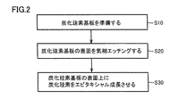
- a method for manufacturing a silicon carbide semiconductor substrate according to the present embodiment includes a step of preparing silicon carbide substrate 1 as a seed substrate (S10), a step of vapor-phase etching main surface 1A of silicon carbide substrate 1 (S20), And a step (S30) of epitaxially growing silicon carbide on the main surface 1A.
- silicon carbide substrate 1 is prepared as a seed substrate.
- Silicon carbide substrate 1 is made of single crystal silicon carbide.
- Silicon carbide substrate 1 has a disk shape with an outer diameter of 4 inches.
- Silicon carbide substrate 1 may have an outer diameter of 4 inches or more, for example, 5 inches or more, or 6 inches or more.
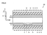
- step (S11) silicon carbide substrate 1 is placed in a vapor phase epitaxial growth apparatus.
- a CVD (Chemical Vapor Deposition) apparatus 100 is used as an example.
- a CVD (Chemical Vapor Deposition) apparatus 100 is used as a vapor phase epitaxial growth apparatus.
- the substrate holder 11 is surrounded by an induction heating coil 12, a quartz tube 13, a heat insulating material 14, and a heating element 15.
- the heating element 15 has a hollow structure and forms a reaction chamber therein.
- Substrate holder 11 is provided inside heating element 15, for example, when silicon carbide substrate 1 is placed, main surface 1A (see FIG. 1) of silicon carbide substrate 1 is flush with the inner peripheral surface of the reaction chamber. It is formed to become.
- the substrate holder 11 is disposed in a recess formed on the inner peripheral surface of the heating element 15, for example.
- the heat insulating material 14 is disposed so as to surround the outer periphery of the heating element 15.
- the quartz tube 13 is disposed so as to surround the outer peripheral side of the heat insulating material 14.
- the induction heating coil 12 includes a plurality of coil members and is provided, for example, so as to wind the outer peripheral side of the quartz tube 13.
- the heating element 15 is induction heated by electromagnetic induction.
- the member constituting the reaction chamber (or the heating element 15) of the CVD apparatus 100 is a high-purity carbon member having a low N 2 content as an impurity, even if TaC coating or SiC coating is not applied. Good.
- FIG. 4A to 4D are graphs in which the horizontal axis is time and the vertical axis is defined as follows.
- the vertical axis in FIG. 4 (a) is the temperature in the reaction chamber
- the vertical axis in FIG. 4 (b) is the flow rate of hydrogen introduced into the reaction chamber
- the vertical axis in FIG. 4 (c) is the propane introduced into the reaction chamber.
- the flow rate was set, and the vertical axis in FIG. 4D was the flow rate of silane and dopant gas introduced into the reaction chamber.
- the reaction chamber in which the silicon carbide substrate 1 is disposed is vacuum baked (period I in FIG. 4). Specifically, referring to FIG. 4A, the reaction chamber is evacuated to an atmospheric pressure of 5 ⁇ 10 ⁇ 14 Pa, and the temperature of the reaction chamber is increased to 1100 ° C. by the heating element 15. (Period I in FIG. 4). After evacuation and temperature rise, the state is maintained from time tp1 as vacuum baking until time tp2 (for example, 10 minutes) (period II in FIG. 4).
- the main surface 1A of the silicon carbide substrate 1 prepared in the previous step (S10) is vapor-phase etched.
- Vapor phase etching is performed to remove foreign substances adhering to and deposited on main surface 1A before epitaxially growing silicon carbide on main surface 1A of silicon carbide substrate 1 (before the next step (S30)).
- the foreign matter adhering and depositing on main surface 1A of silicon carbide substrate 1 is, for example, a reaction product adhering to the inside of the vapor phase epitaxial growth apparatus.
- step (S20) is a vapor phase used in the next step (S30). This is performed following the previous step (S12) using an epitaxial growth apparatus.
- step (S20) main surface 1A of silicon carbide substrate 1 is etched with hydrogen (H 2 ) (step (S21), periods III and IV in FIG. 4).
- hydrogen is introduced into the reaction chamber from time tp ⁇ b> 2 through the piping 16 (see FIG. 3) in the CVD apparatus 100.
- hydrogen used in this step (S21) has the same component and concentration as hydrogen used as a carrier gas in epitaxial growth.
- the flow rate of the hydrogen gas used in this step (S21) is increased from the time point tp2 to the time point tp3, so that it finally becomes equal to the flow rate of the hydrogen gas used as the carrier gas in the next step (S30).
- the temperature in the reaction chamber is further raised from 1100 ° C. to the growth temperature 1580 ° C. in the next step (S30) from time tp2 to time tp3.
- the hydrogen supplied onto main surface 1A of silicon carbide substrate 1 reacts with carbon and silicon constituting main surface 1A of silicon carbide substrate 1 to generate gas phase hydrocarbons and hydrogen silicide. Then, by evacuating the hydrocarbons or hydrogen silicides, foreign substances made of carbides or silicides adhered or deposited on the main surface 1A of the silicon carbide substrate 1 or formed on the main surface 1A of the silicon carbide substrate 1 are formed. Thus, it is possible to reliably remove the defects. In this step (S21), foreign substances made of carbide or silicide adhering and depositing on main surface 1A of silicon carbide substrate 1 and defects formed on main surface 1A of silicon carbide substrate 1 are removed. Carry out until it is surely removed.
- vapor phase etching on main surface 1A of silicon carbide substrate 1 proceeds also in the temperature rising stage of the temperature in the reaction chamber shown in period III (period between time tp3 and time tp4) in FIG. After raising the temperature to the epitaxial growth temperature (1580 ° C.) shown in the middle period IV (period between time tp4 and time tp5), the effect of vapor phase etching is enhanced.
- the time t1 during which vapor-phase etching is performed between the temperature rise and the start of epitaxial growth (the time from time tp3 to time tp5), that is, the process including the step (S22) described later.
- the processing time t1 of the phase etching step (S20) may be longer than the time necessary to surely remove the foreign matters and defects on the main surface 1A, and more preferably, the main surface 1A of the silicon carbide substrate 1 It is set so that the time is less than the time when the roughness is unacceptable.
- the processing time t1 of the vapor phase etching step (S20) in this embodiment is 10 minutes.
- propane (C 3 H 8 ) is further introduced into the reaction chamber as a gas containing carbon atoms from time tp4 (step (S22), period V in FIG. 4).
- propane is introduced into the reaction chamber in addition to hydrogen through the piping 16 in the CVD apparatus 100.
- the propane used in this step (S22) has the same components and concentration as the propane used as the source gas in the next step (S30) no epitaxial growth.
- the flow rate of propane used in this step (S22) is set equal to the flow rate of propane when used as a raw material gas in the next step (S30).
- the hydrogen introduced into the reaction chamber in this step (S22) has the same conditions as in the previous step (S21).
- the temperature in the reaction chamber in this step (S22) is maintained at 1580 ° C., which is a temperature capable of epitaxial growth of silicon carbide, as in the previous step (S21).
- time t2 time from time tp4 to time tp5 for performing this step (S22) is, for example, 10 seconds.
- the propane introduced into the reaction chamber in this step (S22) is thermally decomposed to generate carbon atoms.
- the carbon atoms are supplied to main surface 1A of silicon carbide substrate 1 heated to about 1580 ° C. together with the hydrogen atoms continuously supplied from the previous step (S21). Some of the supplied carbon atoms react with hydrogen atoms to become hydrocarbons and are exhausted, but the remaining part is considered to be bonded to silicon atoms on main surface 1A of silicon carbide substrate 1.
- this step (S22) the amount of hydrogen supplied to main surface 1A of silicon carbide substrate 1 and contributing to vapor-phase etching is reduced as compared with the previous step (S21), so that the silicon carbide substrate.
- etching 1 main surface 1A is reduced. Further, in this step (S22), carbon atoms are supplied to main surface 1A of silicon carbide substrate 1 under a temperature condition in which silicon carbide can be epitaxially grown. Therefore, more carbon atoms are removed in the previous step (S21). It is considered that carbon atoms can be introduced into the main surface 1A thus obtained, and as a result, the main surface 1A in a state more suitable for epitaxial growth can be obtained.
- silicon carbide is epitaxially grown on main surface 1A of silicon carbide substrate 1 as step (S30) from time tp5. Specifically, after performing the previous step (S22) for 10 seconds, the hydrogen and propane conditions in the step (S22) and the temperature conditions in the reaction chamber are maintained, and the silicon carbide is used for epitaxial growth from time tp5. Monosilane (SiH 4 ) as another source gas and a dopant gas containing ammonia (NH 3 ) and / or nitrogen (N 2 ) are further introduced into the reaction chamber. Thereby, epitaxial layer 2 made of silicon carbide is grown on main surface 1A of silicon carbide substrate 1.
- main surface 2A of silicon carbide semiconductor substrate 10 obtained by the method for manufacturing the silicon carbide carrier according to the present embodiment can be a flat surface with little roughness.
- main surface 1A of silicon carbide substrate 1 (S20)
- main surface 1A is vapor-phase etched only with hydrogen.
- foreign matters made of carbide or silicide adhering to and deposited on main surface 1A and defects formed on main surface 1A of silicon carbide substrate 1 can be reliably removed.
- propane is supplied into the reaction chamber from time tp4 in addition to hydrogen. Carbon atoms can be introduced into the surface 1A.
- silicon carbide semiconductor substrate 10 according to the present embodiment obtained by epitaxially growing silicon carbide on main surface 1A is a conventional silicon carbide semiconductor substrate that is epitaxially grown after vapor phase etching using a mixed gas of hydrogen and propane.
- main surface 1A can be a flat surface with little roughness.
- the method for manufacturing a silicon carbide semiconductor substrate according to the present embodiment is more epitaxially grown than a silicon carbide semiconductor substrate obtained by another conventional silicon carbide semiconductor substrate manufacturing method that is epitaxially grown after vapor-phase etching using only hydrogen. Since carbon atoms can be introduced into the main surface 1A before, the main surface 2A after growth can be a flat surface with little roughness.
- the processing time t2 of the step (S22) is 10 seconds, but is not limited thereto.
- the lower limit value of the processing time t2 may be set to, for example, 5 seconds or more from the example described later.
- the upper limit value of the processing time t2 in the step (S22) includes a step (S21) of performing vapor phase etching of the main surface 1A of the silicon carbide substrate 1 only with hydrogen, and the processing time t1 of the entire step (S20). May be set as an arbitrary time that is equal to or shorter than the processing time t1.
- the upper limit value of the processing time t2 is 20 seconds.
- main surface 2A of silicon carbide semiconductor substrate 10 obtained can be a flat surface with little roughness.
- the amount of propane used is reduced by setting the processing time t2 of step (S22) as the necessary and sufficient time as described above, and the flat main surface 2A with less roughness. It is preferable to realize silicon carbide semiconductor substrate 10 having:
- step (S20) H 2 is used as an etching gas when the main surface 1A of silicon carbide substrate 1 is subjected to vapor phase etching, but the present invention is not limited to this.
- vapor phase etching may be performed using hydrogen chloride (HCl) or chlorine (Cl 2 ). Even in this way, foreign matters made of carbide or silicide adhering and depositing on main surface 1A and defects formed on main surface 1A of silicon carbide substrate 1 can be reliably removed.
- propane is used as a gas containing the carbon atom in a process (S22), it is not restricted to this.
- butane (C 4 H 10 ) or methane (CH 4 ) may be used as the gas containing carbon atoms.
- carbon atoms can be introduced into main surface 1A of silicon carbide substrate 1 in the step (S22).
- the flow rate of hydrogen is set to be the same as the flow rate as the carrier gas in the step (S30) from the step (S21) to the step (S30), but is not limited thereto.
- the flow rate of propane was set to be the same as the flow rate as the raw material gas in the step (S30) from the step (S22) to the step (S30), it is not limited to this.
- the temperature in the reaction chamber was set to be the same as the growth temperature in the step (S30) from the step (S21) to the step (S30), the temperature is not limited to this. Each condition can be changed as appropriate. However, as shown in FIG.
- step (S21) it is preferable to perform the continuous processing from the step (S21) to the step (S30) without changing the conditions such as the temperature condition and the gas flow rate so much. In this way, the vapor phase etching process and the epitaxial growth process can be performed under stable conditions.
- a method for manufacturing a silicon carbide semiconductor substrate includes a step of preparing a seed substrate (silicon carbide substrate 1) (step (S10)) and a surface (main surface 1A) of the seed substrate (silicon carbide substrate 1).
- a step of vapor phase etching step (S20)) and a step of epitaxially growing silicon carbide on the surface (main surface 1A) (step (S30)).
- a carbon atom-containing gas is supplied to the seed substrate (silicon carbide substrate 1) from the middle of the vapor phase etching step (step (S20)).
- the vapor-phase etching step (step (S20)) can surely remove the foreign matter adhering to and deposited on main surface 1A of silicon carbide substrate 1, and carbon dioxide from the middle of the vapor-phase etching step.
- An atom-containing gas can be supplied to main surface 1 ⁇ / b> A of silicon carbide substrate 1.
- carbon atoms constituting main surface 1A react with hydrogen atoms with a higher probability than silicon atoms and are removed as hydrocarbons by performing vapor phase etching. For this reason, carbon atoms are insufficient on the main surface 1A, and it is considered that the composition ratio between carbon atoms and silicon atoms deviates from an optimum value as a seed substrate.
- main surface 2 ⁇ / b> A of silicon carbide semiconductor substrate 10 obtained by epitaxial growth on main surface 1 ⁇ / b> A in this state may become rough and flatness may be deteriorated. Therefore, after performing sufficient vapor phase etching, vapor phase etching can be performed in an atmosphere containing carbon atoms by further performing vapor phase etching with carbon atoms supplied to main surface 1A. At this time, by performing vapor phase etching of main surface 1A in an atmosphere containing carbon atoms, the partial pressure of carbon atoms increases in the vicinity of main surface 1A, and vapor phase etching of carbon atoms constituting silicon carbide on main surface 1A is performed. The removal effect is suppressed. As a result, silicon carbide semiconductor substrate 10 having a flat main surface with less surface roughness can be obtained by epitaxially growing silicon carbide on main surface 1A.
- carbon atoms in the carbon atom-containing gas may be introduced into the surface (main surface 1A) of the seed substrate (silicon carbide substrate 1).
- the main surface 1A As described above, by supplying carbon atoms in the step (S22) to the main surface 1A in the gas phase etching step (step (S20)) considered to be deficient in carbon atoms, the main surface 1A It is considered that not only the removal effect of the vapor phase etching on the carbon atoms constituting the silicon carbide can be suppressed, but also the carbon atoms of the vapor phase etching can be introduced into the main surface 1A.
- the carbon atom-containing gas may be one of source gases used in the epitaxial growth step (step (S30)).
- step (S20) the step of vapor phase etching (step (S20)) and the step of epitaxially growing silicon carbide (step (S30)) can be easily and continuously performed.
- step (S30) roughening of main surface 2A of silicon carbide semiconductor substrate 10 obtained by epitaxial growth can be more effectively suppressed.
- the flow rate of the carbon atom-containing gas in the gas phase etching step (step (S20)) may be equal to the flow rate of the carbon atom-containing gas in the epitaxial growth step (step (S30)).
- step (S20) the step of vapor-phase etching (step (S20)) and the step of epitaxially growing silicon carbide (step (S30)) can be performed more easily and continuously.
- step (S20) As shown in step (S22), a carbon atom-containing gas is supplied to the seed substrate (silicon carbide substrate 1) for 10 seconds or more and then epitaxially grown (step) (S30)) may be performed.
- the main surface 2A of the silicon carbide semiconductor substrate 10 can be made a flat surface with less roughness than in the examples described later.
- Example 1 A silicon carbide semiconductor substrate according to Example 1 was produced by the following method.
- a silicon carbide substrate having an outer diameter of 4 inches and a thickness of 350 ⁇ m was prepared.
- the silicon carbide substrate was placed on a substrate holder of a CVD apparatus, and vacuum baking was performed for about 10 minutes at a temperature of 1100 ° C. in the reaction chamber.
- hydrogen was introduced into the reaction chamber at a flow rate of 50 sccm, and the temperature in the reaction chamber was raised to 1580 ° C.
- propane was fed into the reaction chamber 9 minutes and 50 seconds later.
- the flow rate of propane was 30 sccm.
- an epitaxial layer of silicon carbide having an impurity concentration of 1.0 ⁇ 10 18 cm ⁇ 3 and a thickness of 0.5 ⁇ m was formed.
- the NH 3 flow rate was 0.05 sccm.
- the epitaxial growth of silicon carbide was performed at a pressure in the reaction chamber of 8 ⁇ 10 3 Pa to 12 ⁇ 10 3 Pa.
- Example 2 In the silicon carbide semiconductor substrate according to Example 2, the time from when the temperature in the reaction chamber reached 1580 ° C. until propane was supplied into the reaction chamber was 9 minutes 45 seconds, and 15 seconds after the start of propane supply, Supply of dopant gas containing silane and NH 3 was started. The other conditions were the same as in Example 1.
- Comparative Example 1 A silicon carbide semiconductor substrate according to Comparative Example 1 was produced by the following method. First, a silicon carbide substrate having an outer diameter of 4 inches and a thickness of 350 ⁇ m was prepared.
- the silicon carbide substrate was placed on a substrate holder of a CVD apparatus, and vacuum baking was performed for about 10 minutes at a temperature of 1100 ° C. in the reaction chamber. Thereafter, hydrogen was introduced into the reaction chamber at a flow rate of 50 sccm, and the temperature in the reaction chamber was raised to 1580 ° C. After reaching 1580 ° C., propane was fed into the reaction chamber 6 minutes and 50 seconds later. The flow rate of propane was 30 sccm. 190 seconds after the start of supply of propane, supply of a dopant gas containing silane and NH 3 was started, and epitaxial growth of silicon carbide was started on the main surface of the silicon carbide substrate.
- An epitaxial layer of silicon carbide having an impurity concentration of 1.0 ⁇ 10 18 cm ⁇ 3 and a thickness of 0.5 ⁇ m was formed.
- the flow rate of NH 3 was 0.05 sccm.
- the epitaxial growth of silicon carbide was performed at a pressure in the reaction chamber of 8 ⁇ 10 3 Pa to 12 ⁇ 10 3 Pa.
- Comparative Example 2 The silicon carbide semiconductor substrate according to Comparative Example 2 was fabricated under the same conditions as in Example 1 except that the timing for supplying propane into the reaction chamber was the same as the timing for supplying silane. That is, in Comparative Example 2, epitaxial growth of silicon carbide was started after performing vapor phase etching using only hydrogen for 10 minutes.
- the RMS value of the main surface of the silicon carbide semiconductor substrate according to Examples 1 and 2 was 0.8 nm or less.
- the RMS value of the main surface of the silicon carbide semiconductor substrate according to Comparative Example 1 was 1.8 nm.
- the RMS value of the main surface of the silicon carbide semiconductor substrate according to Comparative Example 2 was 2.6 nm.
- the main surface of the silicon carbide semiconductor substrate according to Examples 1 and 2 was less rough and had flatness.
- the main surface of the silicon carbide semiconductor substrate according to Comparative Examples 1 and 2 had a high RMS value and was rough.
Abstract
表面の平坦性が高い炭化珪素半導体基板を低コストで得ることができる炭化珪素半導体基板の製造方法を提供する。種基板としての炭化珪素基板(1)を準備する工程(S10)と、炭化珪素基板(1)の主表面(1A)を気相エッチングする工程(S20)と、主表面(1A)上に炭化珪素をエピタキシャル成長させる工程(S30)とを備える。気相エッチングする工程(S20)の途中から、炭素原子含有ガスを炭化珪素基板1に供給する。
Description
本発明は、炭化珪素半導体基板の製造方法に関し、特に、表面性状の優れた炭化珪素半導体基板の製造方法に関する。
近年、半導体装置の高耐圧化、低損失化などを可能とするため、半導体装置を構成する材料として炭化珪素(SiC)の採用が進められている。炭化珪素は、従来より半導体装置を構成する材料として広く用いられている珪素に比べてバンドギャップが大きいワイドバンドギャップ半導体である。そのため、半導体装置を構成する材料として炭化珪素を採用することにより、半導体装置の高耐圧化、オン抵抗の低減などを達成することができる。また、炭化珪素を材料として採用した半導体装置は、珪素を材料として採用した半導体装置に比べて、高温環境下で使用された場合の特性の低下が小さいという利点も有している。
炭化珪素は、不純物の拡散係数がきわめて低いため、熱拡散処理によって不純物のドーピングを行うことは困難である。炭化珪素材料に活性領域を形成する方法として、エピタキシャル成長層にイオン注入する方法や、ドーパントガスによる不純物添加を伴ったエピタキシャル成長方法が存在する。
炭化珪素のエピタキシャル成長は、種基板として炭化珪素単結晶基板上に行われる。このとき、炭化珪素単結晶基板の表面に対して機械的研磨や化学的研磨などを施して表面処理を行った後、当該表面上にエピタキシャル膜を成長させている。そのため、上記表面処理に起因して、炭化珪素単結晶基板の表面には研磨痕や荒れが生じる場合がある。
また、炭化珪素単結晶基板の表面は平坦化されている場合でも、当該炭化珪素単結晶基板の表面上に炭化珪素をエピタキシャル成長させる際に、気相エピタキシャル成長装置の反応室内の各部材上に成長または付着していた炭化物、珪化物、および炭化珪素等の異物やパーティクル等が当該表面上に付着もしくは堆積する場合がある。この場合、炭化珪素単結晶基板の表面おいて均一なエピタキシャル成長が阻害されるため、得られる炭化珪素半導体基板の表面は荒れ、平坦性が損なわれるという問題があった。
一般に、上記のような問題に対しては、エピタキシャル成長の前処理として、炭化珪素単結晶基板の表面に対し水素による気相エッチングを施すことが行われている。
水素は、炭化珪素単結晶基板の主表面を構成する炭素および珪素と反応して、気相の炭化水素や珪化水素を生じる。そのため、当該炭化水素や珪化水素を排気することで、炭化珪素単結晶基板の主表面上に付着、堆積している炭化物や珪化物からなる異物や、炭化珪素単結晶基板の主表面上に形成されている欠陥を除去することができる。
しかしながら、このとき炭化珪素単結晶基板の表面上の清浄な領域もエッチングされる。さらにこのとき、炭素原子と珪素原子とでは水素原子との反応速度が異なるため、気相エッチング後の炭化珪素単結晶基板の主表面は荒れた状態となる場合があった。
そのため、上述のように、表面の異物や欠陥除去のために水素による気相エッチングを施した炭化珪素単結晶基板の主表面上に炭化珪素をエピタキシャル成長させた場合、得られる炭化珪素半導体基板の表面は荒れてしまい、平坦化することは困難であった。
表面の平坦性の高い炭化珪素単結晶基板を作製する方法として、特開2005-64383号公報には、表面の平坦性の高い炭化珪素のエピタキシャルウエハを作製する方法として、基板表面を1400℃~1600℃の水素ガスとプロパンガスの混合ガスにより清浄化する方法が開示されている。
しかしながら、炭化珪素からなる種基板の基板温度を1400℃以上として、当該表面を水素とプロパンとの混合ガスにより気相エッチングして、当該表面上の異物や欠陥を除去する場合、異物や欠陥の種類によっては気相エッチングによる除去効果が低下する可能性があると考えられる。
これは以下の理由による。上述のように、気相エッチングにおける水素は、炭化珪素を構成する炭素原子および珪素原子とそれぞれ反応して、気相の炭化水素および珪化水素を生じる。このとき、炭素原子の供給源となるプロパンがエッチング雰囲気中に供給されていると、炭素原子を含む異物等に対する除去効果が低下する可能性が考えられるためである。
また、プロパンの使用量が増加することにより、炭化珪素半導体基板の製造コストが高くなる。
本発明は、上記のような課題を解決するためになされたものである。本発明の主たる目的は、表面の平坦性が高い炭化珪素半導体基板を低コストで得ることができる炭化珪素半導体基板の製造方法を提供することにある。
本発明者らは、上記課題を解決するため鋭意研究を重ねた結果、種基板の表面に対して水素のみを用いた気相エッチングを実施するとともに、その途中から炭素原子を含有するガスをさらに供給した場合において、当該表面上に炭化珪素をエピタキシャル成長させて得られた炭化珪素半導体基板は平坦性の高い表面を有することを見出した。
本発明の炭化珪素半導体基板の製造方法は、種基板を準備する工程と、種基板の表面を気相エッチングする工程と、表面上に炭化珪素をエピタキシャル成長させる工程とを備え、気相エッチングする工程の途中から、炭素原子含有ガスを種基板に供給する。気相エッチングする工程では、水素原子を含むガスを用いることが好ましい。
これにより、気相エッチング工程により、炭化珪素基板1の主表面に付着、堆積した異物等を確実に除去することができるとともに、当該気相エッチング工程の途中から炭素原子含有ガスを炭化珪素基板1の主表面に供給することができる。
このとき、主表面を構成する炭素原子は、水素原子を含むガスを用いて気相エッチングされることにより、珪素原子よりも高い確率で水素原子と反応して炭化水素として除去される。そのため、主表面において炭素原子は不足し、炭素原子と珪素原子との組成比は種基板として最適な値から乖離していると考えられる。実際、この状態の主表面上にエピタキシャル成長して得られる炭化珪素半導体基板の主表面は、荒れてしまい、平坦性が悪くなることを発明者らは確認している。
そのため、十分な気相エッチングを行った上で、さらに主表面に炭素原子を供給した状態で気相エッチングすることにより、気相エッチングを炭素原子を含む雰囲気下で実施する。このようにすれば、主表面上近傍で炭素原子の分圧が上がり、主表面の炭化珪素を構成する炭素原子に対する、気相エッチングによる除去効果が抑えられる。その結果、当該主表面の炭素原子と珪素原子の組成比や表面性状をエピタキシャル成長にとり好適な状態とすることができる。そのため、当該主表面上に炭化珪素をエピタキシャル成長させることで、表面の荒れの少ない平坦な主表面を有する炭化珪素半導体基板を得ることができる。
本発明によれば、表面が平坦な炭化珪素半導体基板を低コストで作製することができる。
以下、本発明の実施の形態に係る炭化珪素半導体基板の製造方法について説明する。まず、図1を参照して、本実施の形態に係る炭化珪素半導体基板10について説明する。本実施の形態に係る炭化珪素半導体基板10は、種基板としての炭化珪素基板1と、炭化珪素基板1上にエピタキシャル成長された炭化珪素からなるエピタキシャル層2を備える。
炭化珪素基板1は、たとえば単結晶炭化珪素からなる。単結晶炭化珪素は、たとえば六方晶の結晶構造を有している。炭化珪素基板1は主表面1Aを含んでいる。炭化珪素基板1の主表面1Aは平坦化されており、原子間力顕微鏡(AFM)を用いて測定した二乗平均面粗さ(RMS値)は0.2nm以下である。
エピタキシャル層2は、炭化珪素基板1の主表面1A上に形成されている。エピタキシャル層2は、たとえば、導電型がn型である。エピタキシャル層2におけるn型の不純物濃度は、1×1018cm-3以上3×1018cm-3以下程度である。エピタキシャル層2は主表面2Aを含んでいる。
次に、図1および図2を参照して、上記の炭化珪素半導体基板10を製造するための、本実施の形態の炭化珪素半導体基板の製造方法を説明する。本実施の形態に係る炭化珪素半導体基板の製造方法は、種基板としての炭化珪素基板1を準備する工程(S10)と、炭化珪素基板1の主表面1Aを気相エッチングする工程(S20)と、当該主表面1A上に炭化珪素をエピタキシャル成長させる工程(S30)とを備える。
まず、工程(S10)では、種基板として炭化珪素基板1を準備する。炭化珪素基板1は、単結晶炭化珪素からなる。炭化珪素基板1は、外径が4インチの円板形状である。なお、炭化珪素基板1の外径は、4インチ以上、たとえば、5インチ以上、もしくは6インチ以上であってもよい。
次に、工程(S11)では、気相エピタキシャル成長装置内に炭化珪素基板1を配置する。本実施の形態においては、一例として、CVD(Chemical Vapor Deposition)装置100を用いている。
図3を参照して、本実施の形態では、気相エピタキシャル成長装置として、CVD(Chemical Vapor Deposition)装置100を用いる。CVD装置100において、基板ホルダ11は、その周囲を誘導加熱用コイル12と、石英管13と、断熱材14と、発熱体15とによって囲まれている。具体的には、発熱体15は中空構造であって、内部に反応室を形成している。基板ホルダ11は、発熱体15の内部に設けられ、たとえば、炭化珪素基板1を載置したときに、炭化珪素基板1の主表面1A(図1参照)が反応室の内周表面と同一平面となるように形成されている。基板ホルダ11は、たとえば発熱体15の内周表面に形成された凹部内に配置されている。断熱材14は、発熱体15の外周囲を囲うように配置されている。石英管13は、断熱材14の外周側を囲うように配置されている。誘導加熱用コイル12は、複数のコイル部材を含み、たとえば、石英管13の外周側を巻回するように設けられている。誘導加熱用コイル12を高周波コイルとしてこれに高周波電流を流すと、電磁誘導作用により、発熱体15は誘導加熱される。これにより、炭化珪素基板1および炭化珪素基板1に供給される原料ガス等を所定の温度に加熱することができる。
このとき、CVD装置100の反応室(あるいは発熱体15)を構成する部材は、不純物としてのN2含有量の低い高純度のカーボン部材であり、TaCコートやSiCコートが施されていなくてもよい。
次に、図4を参照して、CVD装置内において実施される工程(S12)~工程(S30)について説明する。図4(a)~図4(d)は、横軸を時間として、縦軸をそれぞれ次のように規定したグラフである。図4(a)の縦軸は反応室内の温度とし、図4(b)の縦軸は反応室内に導入した水素の流量とし、図4(c)の縦軸は反応室内に導入したプロパンの流量とし、図4(d)の縦軸は反応室内に導入したシランおよびドーパントガスの流量とした。
工程(S12)として、炭化珪素基板1を配置した反応室内を真空ベークする(図4中の期間I)。具体的には、図4(a)を参照して、反応室内を排気して反応室内の雰囲気圧力を5×10-14Paとし、さらに発熱体15によって反応室内の温度を1100℃まで昇温させる(図4中の期間I)。排気および昇温後、時点tp1から真空ベークとして当該状態を時点tp2まで(たとえば10分間)維持する(図4中の期間II)。
次に、工程(S20)では、先の工程(S10)で準備した炭化珪素基板1の主表面1Aを気相エッチングする。気相エッチングは、炭化珪素基板1の主表面1A上に炭化珪素をエピタキシャル成長する前に(次工程(S30)の前に)、当該主表面1A上に付着、堆積した異物を除去するために行われる。ここで、炭化珪素基板1の主表面1A上に付着、堆積した異物とは、たとえば、気相エピタキシャル成長装置内部に付着していた反応生成物である。炭化珪素基板1の主表面1A上に炭化珪素をエピタキシャル成長する前に、当該主表面1A上に付着、堆積した異物を除去するため、本工程(S20)は、次工程(S30)において用いる気相エピタキシャル成長装置を用いて、先の工程(S12)に続いて実施される。
具体的に、本工程(S20)では、まず、炭化珪素基板1の主表面1Aを水素(H2)によってエッチングする(工程(S21)、図4中の期間III、IV)。具体的には、図4(b)を参照して、CVD装置100内に配管16(図3参照)を介して、時点tp2から反応室内に水素を導入する。このとき、本工程(S21)に用いる水素は、エピタキシャル成長においてキャリアガスとして用いられる水素と同一の成分、濃度とする。さらに、本工程(S21)に用いる水素ガスの流量は、時点tp2から時点tp3まで増やすことで、最終的には次工程(S30)においてキャリアガスとして用いられるときの水素ガスの流量と等しくする。
また、反応室内の温度を、時点tp2から時点tp3にかけて、1100℃から次工程(S30)における成長温度1580℃までさらに昇温する。
これにより、炭化珪素基板1の主表面1A上に供給された水素は、炭化珪素基板1の主表面1Aを構成する炭素および珪素と反応して、気相の炭化水素や珪化水素を生じる。そして、当該炭化水素や珪化水素を排気することで、炭化珪素基板1の主表面1A上に付着、堆積している炭化物や珪化物からなる異物や、炭化珪素基板1の主表面1A上に形成されている欠陥を確実に除去することができる。なお、本工程(S21)は、炭化珪素基板1の主表面1A上に付着、堆積している炭化物や珪化物からなる異物や、炭化珪素基板1の主表面1A上に形成されている欠陥を確実に除去するまで実施する。このとき、炭化珪素基板1の主表面1A上の清浄な領域も水素によりエッチングされるため、主表面1Aにおける当該領域も荒れてしまう。これは、上述のように、炭化珪素を構成する炭素原子と珪素原子のうち、炭素原子は珪素原子より高い確率で水素原子と反応して炭化水素として除去されるため、気相エッチング後の炭化珪素基板1の主表面1Aにおける炭素原子と珪素原子の組成比が1:1ではなくなっているためと考えられる。
なお、図4中の期間III(時点tp3から時点tp4の間の期間)に示す反応室内の温度の昇温段階においても炭化珪素基板1の主表面1Aに対する気相エッチングは進行するが、図4中の期間IV(時点tp4から時点tp5の間の期間)に示すエピタキシャル成長温度(1580℃)に昇温後には、気相エッチングの効果は高まる。本実施の形態においては、昇温後からエピタキシャル成長を開始するまでの間(時点tp3から時点tp5までの時間)に気相エッチングを施す時間t1、つまり、後述する工程(S22)を含めた、気相エッチングする工程(S20)の処理時間t1は、主表面1A上の異物、欠陥を確実に除去するのに必要な時間以上であればよく、より好ましくは、炭化珪素基板1の主表面1Aの荒れが許容できない程度となる時間以下となるように設定する。本実施の形態における気相エッチングする工程(S20)の処理時間t1は、一例として10分とする。
次に、反応室内に、時点tp4から炭素原子を含有するガスとしてプロパン(C3H8)をさらに導入する(工程(S22)、図4中の期間V)。具体的には、図4(b)を参照して、CVD装置100内に配管16を介して、水素に加えてプロパンを反応室内に導入する。このとき、本工程(S22)に用いるプロパンは、次工程(S30)noエピタキシャル成長において原料ガスとして用いられるプロパンと同一の成分、濃度とする。さらに、本工程(S22)に用いるプロパンの流量は、次工程(S30)において原料ガスとして用いられるときのプロパンの流量と等しくする。また、本工程(S22)において反応室に導入される水素は先の工程(S21)と同一条件である。
また、本工程(S22)における反応室内の温度は、先の工程(S21)と同様に、炭化珪素のエピタキシャル成長が可能な温度である1580℃のまま維持しておく。このとき、本工程(S22)を実施する時間t2(時点tp4から時点tp5までの時間)は、たとえば10秒とする。
これにより、本工程(S22)において反応室内に導入されたプロパンは熱分解されて、炭素原子を生じる。当該炭素原子は、先の工程(S21)から連続して供給され続けている水素原子とともに、1580℃程度に加熱された炭化珪素基板1の主表面1Aに供給される。供給された炭素原子のうち一部は水素原子と反応して炭化水素となり排気されるが、残りの一部は炭化珪素基板1の主表面1Aの珪素原子と結合すると考えられる。この結果、本工程(S22)においては、先の工程(S21)と比べて炭化珪素基板1の主表面1Aに供給されて気相エッチングに寄与する水素の量が減少することにより、炭化珪素基板1の主表面1Aをエッチングする効果は低下する。さらに、本工程(S22)において、炭化珪素のエピタキシャル成長が可能な温度条件下で炭化珪素基板1の主表面1Aに炭素原子が供給されるため、先の工程(S21)によって炭素原子がより多く除去された主表面1Aに、炭素原子を導入でき、結果的にエピタキシャル成長により適した状態の主表面1Aを得ることができると考えられる。
次に、工程(S22)と連続して、時点tp5から工程(S30)として炭化珪素基板1の主表面1A上に炭化珪素をエピタキシャル成長させる。具体的には、先の工程(S22)を10秒間実施した後、工程(S22)における水素およびプロパンの各条件、ならびに反応室内の温度条件は維持しながら、時点tp5より炭化珪素のエピタキシャル成長に用いる他の原料ガスとしてのモノシラン(SiH4)と、アンモニア(NH3)および/または窒素(N2)を含むドーパントガスを反応室内にさらに導入する。これにより、炭化珪素基板1の主表面1A上に、炭化珪素からなるエピタキシャル層2を成長させる。
このように、工程(S22)と工程(S30)とを連続して実施することで、工程(S22)において炭化珪素基板1の主表面1Aに対して炭素原子を導入して、主表面1Aの炭素原子と珪素原子の組成比の偏りを緩和した状態で、当該主表面1A上に炭化珪素からなるエピタキシャル層2を成長させることができると考えられる。この結果、本実施の形態に係る炭化珪素搬送体の製造方法により得られた炭化珪素半導体基板10の主表面2Aは、荒れの少ない平坦な面とすることができる。
以上のように、本実施の形態に係る炭化珪素半導体基板の製造方法は、炭化珪素基板1の主表面1Aを気相エッチングする工程(S20)において、主表面1Aを水素のみにより気相エッチングして、主表面1A上に付着、堆積している炭化物や珪化物からなる異物や、炭化珪素基板1の主表面1A上に形成されている欠陥を確実に除去することができる。さらに、図4の期間III、IVのように確実に除去することができるまで水素のみによる気相エッチング工程を実施した後、時点tp4から反応室内に水素に加えてプロパンを供給することにより、主表面1Aに炭素原子を導入することができる。その結果、当該主表面1A上に炭化珪素をエピタキシャル成長させて得られる本実施の形態に係る炭化珪素半導体基板10は、水素とプロパンとの混合ガスによる気相エッチング後にエピタキシャル成長する従来の炭化珪素半導体基板の製造方法で得られる炭化珪素半導体基板と比べて、エピタキシャル成長前に主表面1A上の異物や欠陥が確実に除去できているため、主表面2Aは荒れの少ない平坦な面とすることができる。さらに、本実施の形態に係る炭化珪素半導体基板の製造方法は、水素のみによる気相エッチング後にエピタキシャル成長する従来の他の炭化珪素半導体基板の製造方法で得られる炭化珪素半導体基板と比べても、エピタキシャル成長前に主表面1Aに炭素原子を導入することができるため、成長後の主表面2Aは荒れの少ない平坦な面とすることができる。
本実施の形態においては、工程(S22)の処理時間t2は10秒であったが、これに限られるものではない。処理時間t2の下限値については、後述する実施例より、たとえば5秒以上とすればよい。また、工程(S22)の処理時間t2の上限値は、水素のみにより炭化珪素基板1の主表面1Aを気相エッチングする工程(S21)を備えており、かつ工程(S20)全体の処理時間t1が300秒程度である限りにおいて、処理時間t1以下の任意の時間として設定してもよい。好ましくは、処理時間t2の上限値は20秒である。このようにしても、得られる炭化珪素半導体基板10の主表面2Aを荒れの少ない平坦な面とすることができる。一方で、炭化珪素半導体基板10の製造コストを抑えるという観点から、工程(S22)の処理時間t2を上述のような必要十分な時間としてプロパンの使用量を抑え、荒れの少ない平坦な主表面2Aを有する炭化珪素半導体基板10を実現するのが好ましい。
また、本実施の形態において、工程(S20)は、炭化珪素基板1の主表面1Aを気相エッチングする際に、エッチングガスとしてH2を用いているが、これに限られるものではない。たとえば、塩化水素(HCl)や塩素(Cl2)を用いて気相エッチングを行っても良い。このようにしても、主表面1A上に付着、堆積している炭化物や珪化物からなる異物や、炭化珪素基板1の主表面1A上に形成されている欠陥を確実に除去することができる。
また、本実施の形態において、工程(S22)における炭素原子を含有するガスとしてプロパンを用いているが、これに限られるものではない。たとえば、炭素原子を含有するガスとしてブタン(C4H10)やメタン(CH4)を用いてもよい。このようにしても、工程(S22)において、炭化珪素基板1の主表面1Aに炭素原子を導入することができる。
また、本実施の形態において、工程(S21)から工程(S30)にかけて、水素の流量は工程(S30)におけるキャリアガスとしての流量と同一に設定されていたが、これに限られるものではない。また、工程(S22)から工程(S30)にかけて、プロパンの流量は工程(S30)における原料ガスとしての流量と同一に設定されていたが、これに限られるものではない。また、工程(S21)から工程(S30)にかけて、反応室内の温度は工程(S30)における成長温度と同一に設定されていたが、これに限られるものではない。各条件ともに適宜変更することは可能である。しかし、図4に示すように、工程(S21)から工程(S30)にかけて温度条件やガスの流量などの条件をあまり変動させることなく連続処理するのが好ましい。このようにすれば、安定した条件下で気相エッチング工程およびエピタキシャル成長工程を実施することができる。
ここで、上述した実施の形態と一部重複する部分もあるが、本発明の特徴的な構成を列挙する。
この発明に従った炭化珪素半導体基板の製造方法は、種基板(炭化珪素基板1)を準備する工程(工程(S10))と、種基板(炭化珪素基板1)の表面(主表面1A)を気相エッチングする工程(工程(S20))と、表面(主表面1A)上に炭化珪素をエピタキシャル成長させる工程(工程(S30))とを備える。気相エッチングする工程(工程(S20))の途中から、炭素原子含有ガスを種基板(炭化珪素基板1)に供給する。
これにより、気相エッチングする工程(工程(S20))により、炭化珪素基板1の主表面1Aに付着、堆積した異物等を確実に除去することができるとともに、当該気相エッチング工程の途中から炭素原子含有ガスを炭化珪素基板1の主表面1Aに供給することができる。このとき、主表面1Aを構成する炭素原子は、気相エッチングされることにより、珪素原子よりも高い確率で水素原子と反応して炭化水素として除去される。このため、主表面1Aにおいて炭素原子は不足し、炭素原子と珪素原子との組成比は種基板として最適な値から乖離していると考えられる。具体的には、この状態の主表面1A上にエピタキシャル成長して得られる炭化珪素半導体基板10の主表面2Aは、荒れてしまい、平坦性が悪くなる場合がある。そのため、十分な気相エッチングを行った上で、さらに主表面1Aに炭素原子を供給した状態で気相エッチングすることにより、気相エッチングを炭素原子を含む雰囲気下で実施することができる。このとき、炭素原子を含む雰囲気下で主表面1Aを気相エッチングすることで、主表面1A上近傍で炭素原子の分圧が上がり、主表面1Aの炭化珪素を構成する炭素原子に対する気相エッチングの除去効果が抑えられる。その結果、当該主表面1A上に炭化珪素をエピタキシャル成長させることで、表面の荒れの少ない平坦な主表面を有する炭化珪素半導体基板10を得ることができる。
上記エピタキシャル成長させる工程(工程(S30))に先立って、炭素原子含有ガス中の炭素原子が種基板(炭化珪素基板1)の表面(主表面1A)に導入されていてもよい。
上述のように、炭素原子が不足していると考えられる気相エッチングする工程(工程(S20))における主表面1Aに対して工程(S22)において炭素原子を供給することで、主表面1Aの炭化珪素を構成する炭素原子に対する気相エッチングの除去効果を抑制できるだけでなく、気相エッチングの当該炭素原子を主表面1Aに導入することができると考えられる。
上記炭素原子含有ガスは、エピタキシャル成長させる工程(工程(S30))で用いる原料ガスの一つであってもよい。
このようにすることで、気相エッチングする工程(工程(S20))と炭化珪素をエピタキシャル成長する工程(工程(S30))とを容易に連続して実施することができる。連続して実施することにより、より効果的に、エピタキシャル成長により得られる炭化珪素半導体基板10の主表面2Aの荒れを抑制できる。
上記気相エッチングする工程(工程(S20))における炭素原子含有ガスの流量は、エピタキシャル成長させる工程(工程(S30))での炭素原子含有ガスの流量と等しくてもよい。
このようにすることで、気相エッチングする工程(工程(S20))と炭化珪素をエピタキシャル成長する工程(工程(S30))とをさらに容易に連続して実施することができる。
上記気相エッチングする工程(工程(S20))において、工程(S22)に示すように炭素原子含有ガスを種基板(炭化珪素基板1)に10秒以上供給した後、続けてエピタキシャル成長させる工程(工程(S30))を実施してもよい。
このようにすれば、後述する実施例より、炭化珪素半導体基板10の主表面2Aを荒れの少ない、平坦な面とすることができる。
以下、本発明の実施例について説明する。
(実施例1)
本実施例1に係る炭化珪素半導体基板を以下の方法で作製した。
(実施例1)
本実施例1に係る炭化珪素半導体基板を以下の方法で作製した。
まず、外径が4インチで厚みが350μmの炭化珪素基板を準備した。
次に、当該炭化珪素基板をCVD装置の基板ホルダに配置して、反応室内の温度を1100℃とする真空ベークを約10分実施した。その後、反応室内に水素を流量50sccm導入するとともに、反応室内の温度を1580℃まで昇温させた。1580℃に到達してから、9分50秒後に反応室内にプロパンの供給を開始した。プロパンの流量は、30sccmとした。プロパンの供給開始から10秒後に、シランおよびNH3を含むドーパントガスの供給を開始して、当該炭化珪素基板の主表面上に炭化珪素のエピタキシャル成長を開始した。
次に、当該炭化珪素基板をCVD装置の基板ホルダに配置して、反応室内の温度を1100℃とする真空ベークを約10分実施した。その後、反応室内に水素を流量50sccm導入するとともに、反応室内の温度を1580℃まで昇温させた。1580℃に到達してから、9分50秒後に反応室内にプロパンの供給を開始した。プロパンの流量は、30sccmとした。プロパンの供給開始から10秒後に、シランおよびNH3を含むドーパントガスの供給を開始して、当該炭化珪素基板の主表面上に炭化珪素のエピタキシャル成長を開始した。
このようにして、不純物濃度が1.0×1018cm-3、厚さ0.5μmの炭化珪素のエピタキシャル層を形成した。なお、NH3の流量は0.05sccmとした。炭化珪素のエピタキシャル成長は、反応室内の圧力を8×10³Pa以上12×103Pa以下として実施した。
(実施例2)
実施例2に係る炭化珪素半導体基板は、反応室内の温度が1580℃に到達してから、反応室内にプロパンを供給するまでの時間を9分45秒とし、プロパンの供給開始から15秒後に、シランおよびNH3を含むドーパントガスの供給を開始した。それ以外の条件は実施例1と同条件として作製した。
実施例2に係る炭化珪素半導体基板は、反応室内の温度が1580℃に到達してから、反応室内にプロパンを供給するまでの時間を9分45秒とし、プロパンの供給開始から15秒後に、シランおよびNH3を含むドーパントガスの供給を開始した。それ以外の条件は実施例1と同条件として作製した。
(比較例1)
比較例1に係る炭化珪素半導体基板を以下の方法で作製した。まず、外径が4インチで厚みが350μmの炭化珪素基板を準備した。
比較例1に係る炭化珪素半導体基板を以下の方法で作製した。まず、外径が4インチで厚みが350μmの炭化珪素基板を準備した。
次に、当該炭化珪素基板をCVD装置の基板ホルダに配置して、反応室内の温度を1100℃とする真空ベークを約10分実施した。その後、反応室内に水素を流量50sccm導入するとともに、反応室内の温度を1580℃まで昇温させた。1580℃に到達してから、6分50秒後に反応室内にプロパンの供給を開始した。プロパンの流量は、30sccmとした。プロパンの供給開始から190秒後に、シランおよびNH3を含むドーパントガスの供給を開始して、当該炭化珪素基板の主表面上に炭化珪素のエピタキシャル成長を開始した。
不純物濃度が1.0×1018cm-3、厚さ0.5μmの炭化珪素のエピタキシャル層を形成した。NH3の流量は0.05sccmとした。炭化珪素のエピタキシャル成長は、反応室内の圧力を8×10³Pa以上12×103Pa以下として実施した。
(比較例2)
比較例2に係る炭化珪素半導体基板は、反応室内にプロパンを供給するタイミングはシランを供給するタイミングと同時とし、それ以外の条件は実施例1と同条件として作製した。つまり、比較例2においては、水素のみによる気相エッチングを10分間実施した後、炭化珪素のエピタキシャル成長を開始した。
比較例2に係る炭化珪素半導体基板は、反応室内にプロパンを供給するタイミングはシランを供給するタイミングと同時とし、それ以外の条件は実施例1と同条件として作製した。つまり、比較例2においては、水素のみによる気相エッチングを10分間実施した後、炭化珪素のエピタキシャル成長を開始した。
(評価)
実施例1、2および比較例1、2に係る炭化珪素半導体基板の主表面に対し、AFM(NanoScopeIII)を用いて二乗平均面粗さ(RMS値)を測定した。
実施例1、2および比較例1、2に係る炭化珪素半導体基板の主表面に対し、AFM(NanoScopeIII)を用いて二乗平均面粗さ(RMS値)を測定した。
(結果)
実施例1、2に係る炭化珪素半導体基板の主表面のRMS値は0.8nm以下であった。一方、比較例1に係る炭化珪素半導体基板の主表面のRMS値は1.8nmであった。比較例2に係る炭化珪素半導体基板の主表面のRMS値は2.6nmであった。
実施例1、2に係る炭化珪素半導体基板の主表面のRMS値は0.8nm以下であった。一方、比較例1に係る炭化珪素半導体基板の主表面のRMS値は1.8nmであった。比較例2に係る炭化珪素半導体基板の主表面のRMS値は2.6nmであった。
つまり、実施例1、2に係る炭化珪素半導体基板の主表面は、荒れが少なく、平坦性を有していた。一方、比較例1、2に係る炭化珪素半導体基板の主表面は、RMS値が高く、荒れていた。
以上のように本発明の実施の形態および実施例について説明を行なったが、上述の実施の形態および実施例を様々に変形することも可能である。また、本発明の範囲は上述の実施の形態および実施例に限定されるものではない。本発明の範囲は、請求の範囲によって示され、請求の範囲と均等の意味および範囲内でのすべての変更を含むことが意図される。
1 炭化珪素基板、1A,2A 主表面、2 エピタキシャル層、10 炭化珪素半導体基板、11 基板ホルダ、12 誘導加熱用コイル、13 石英管、14 断熱材、15 発熱体、16 配管、100 CVD装置。
Claims (5)
- 種基板を準備する工程と、
前記種基板の表面を気相エッチングする工程と、
前記表面上に炭化珪素をエピタキシャル成長させる工程とを備え、
前記気相エッチングする工程の途中から、炭素原子含有ガスを前記種基板に供給する、炭化珪素半導体基板の製造方法。 - 前記エピタキシャル成長させる工程に先立って、前記炭素原子含有ガス中の炭素原子が前記種基板の前記表面に導入されている、請求項1に記載の炭化珪素半導体基板の製造方法。
- 前記炭素原子含有ガスは、前記エピタキシャル成長させる工程で用いる原料ガスの一つである、請求項1または請求項2に記載の炭化珪素半導体基板の製造方法。
- 前記気相エッチングする工程における前記炭素原子含有ガスの流量は、前記エピタキシャル成長させる工程での前記炭素原子含有ガスの流量と等しい、請求項3に記載の炭化珪素半導体基板の製造方法。
- 前記気相エッチングする工程において、前記炭素原子含有ガスを前記種基板に10秒以上供給した後、続けて前記エピタキシャル成長させる工程を実施する、請求項1~請求項4のいずれか1項に記載の炭化珪素半導体基板の製造方法。
Priority Applications (2)
| Application Number | Priority Date | Filing Date | Title |
|---|---|---|---|
| CN201480009899.1A CN105705684A (zh) | 2013-03-27 | 2014-03-26 | 制造碳化硅半导体衬底的方法 |
| US14/647,774 US9269572B2 (en) | 2013-03-27 | 2014-03-26 | Method for manufacturing silicon carbide semiconductor substrate |
Applications Claiming Priority (2)
| Application Number | Priority Date | Filing Date | Title |
|---|---|---|---|
| JP2013-066491 | 2013-03-27 | ||
| JP2013066491A JP2014189442A (ja) | 2013-03-27 | 2013-03-27 | 炭化珪素半導体基板の製造方法 |
Publications (1)
| Publication Number | Publication Date |
|---|---|
| WO2014157332A1 true WO2014157332A1 (ja) | 2014-10-02 |
Family
ID=51624295
Family Applications (1)
| Application Number | Title | Priority Date | Filing Date |
|---|---|---|---|
| PCT/JP2014/058524 WO2014157332A1 (ja) | 2013-03-27 | 2014-03-26 | 炭化珪素半導体基板の製造方法 |
Country Status (4)
| Country | Link |
|---|---|
| US (1) | US9269572B2 (ja) |
| JP (1) | JP2014189442A (ja) |
| CN (1) | CN105705684A (ja) |
| WO (1) | WO2014157332A1 (ja) |
Families Citing this family (1)
| Publication number | Priority date | Publication date | Assignee | Title |
|---|---|---|---|---|
| KR102265623B1 (ko) * | 2018-12-26 | 2021-06-22 | 한국세라믹기술원 | 증착공정에서 발생되는 탄화규소 부산물의 재생 방법 |
Citations (6)
| Publication number | Priority date | Publication date | Assignee | Title |
|---|---|---|---|---|
| WO2006022282A1 (ja) * | 2004-08-24 | 2006-03-02 | Bridgestone Corporation | 炭化ケイ素単結晶ウェハ及びその製造方法 |
| JP2008222509A (ja) * | 2007-03-14 | 2008-09-25 | Matsushita Electric Ind Co Ltd | SiCエピタキシャル膜付き単結晶基板の製造方法 |
| JP2009274899A (ja) * | 2008-05-13 | 2009-11-26 | Toyota Motor Corp | 炭化珪素エピタキシャル用基板の製造方法 |
| JP2010095431A (ja) * | 2008-10-20 | 2010-04-30 | Toyota Motor Corp | SiC薄膜形成装置 |
| WO2010087518A1 (ja) * | 2009-01-30 | 2010-08-05 | 新日本製鐵株式会社 | エピタキシャル炭化珪素単結晶基板及びその製造方法 |
| WO2012067112A1 (ja) * | 2010-11-17 | 2012-05-24 | 新日本製鐵株式会社 | エピタキシャル炭化珪素単結晶基板の製造方法 |
Family Cites Families (18)
| Publication number | Priority date | Publication date | Assignee | Title |
|---|---|---|---|---|
| JP4238357B2 (ja) | 2003-08-19 | 2009-03-18 | 独立行政法人産業技術総合研究所 | 炭化珪素エピタキシャルウエハ、同ウエハの製造方法及び同ウエハ上に作製された半導体装置 |
| EP1739726A4 (en) * | 2004-03-26 | 2009-08-26 | Kansai Electric Power Co | BIPOLAR SEMICONDUCTOR DEVICE AND METHOD FOR MANUFACTURING SAME |
| US7312128B2 (en) * | 2004-12-01 | 2007-12-25 | Applied Materials, Inc. | Selective epitaxy process with alternating gas supply |
| US7235492B2 (en) * | 2005-01-31 | 2007-06-26 | Applied Materials, Inc. | Low temperature etchant for treatment of silicon-containing surfaces |
| JP2006321696A (ja) * | 2005-05-20 | 2006-11-30 | Hitachi Cable Ltd | 炭化珪素単結晶の製造方法 |
| US7501349B2 (en) * | 2006-03-31 | 2009-03-10 | Tokyo Electron Limited | Sequential oxide removal using fluorine and hydrogen |
| JP5131675B2 (ja) * | 2006-08-25 | 2013-01-30 | 国立大学法人京都大学 | 炭化ケイ素基板の製造方法 |
| JP5125095B2 (ja) | 2006-12-22 | 2013-01-23 | パナソニック株式会社 | SiCエピタキシャル膜付き基板の製造方法及びSiCエピタキシャル膜付き基板の製造装置 |
| CN100578737C (zh) * | 2008-11-07 | 2010-01-06 | 中国电子科技集团公司第五十五研究所 | 一种制作基本上没有台阶形貌的碳化硅外延层的方法 |
| JP4959763B2 (ja) * | 2009-08-28 | 2012-06-27 | 昭和電工株式会社 | SiCエピタキシャルウェハ及びその製造方法 |
| JP4887418B2 (ja) | 2009-12-14 | 2012-02-29 | 昭和電工株式会社 | SiCエピタキシャルウェハの製造方法 |
| SE1051137A1 (sv) * | 2010-10-29 | 2012-04-30 | Fairchild Semiconductor | Förfarande för tillverkning av en kiselkarbid bipolär transistor och kiselkarbid bipolär transistor därav |
| CN102534808B (zh) * | 2010-12-14 | 2014-11-05 | 北京天科合达蓝光半导体有限公司 | 高质量碳化硅表面的获得方法 |
| EP2750198A4 (en) * | 2011-08-26 | 2015-04-15 | Nat Univ Corp Nara Inst | SiC SEMICONDUCTOR ELEMENT AND METHOD FOR MANUFACTURING THE SAME |
| CN102592976B (zh) * | 2012-03-22 | 2014-04-02 | 西安电子科技大学 | P型重掺杂碳化硅薄膜外延制备方法 |
| US10541306B2 (en) * | 2012-09-12 | 2020-01-21 | Cree, Inc. | Using a carbon vacancy reduction material to increase average carrier lifetime in a silicon carbide semiconductor device |
| US8940614B2 (en) * | 2013-03-15 | 2015-01-27 | Dow Corning Corporation | SiC substrate with SiC epitaxial film |
| CN103614779B (zh) * | 2013-11-28 | 2016-03-16 | 中国电子科技集团公司第五十五研究所 | 一种提高碳化硅外延片片内n型掺杂浓度均匀性的方法 |
-
2013
- 2013-03-27 JP JP2013066491A patent/JP2014189442A/ja active Pending
-
2014
- 2014-03-26 WO PCT/JP2014/058524 patent/WO2014157332A1/ja active Application Filing
- 2014-03-26 US US14/647,774 patent/US9269572B2/en active Active
- 2014-03-26 CN CN201480009899.1A patent/CN105705684A/zh active Pending
Patent Citations (6)
| Publication number | Priority date | Publication date | Assignee | Title |
|---|---|---|---|---|
| WO2006022282A1 (ja) * | 2004-08-24 | 2006-03-02 | Bridgestone Corporation | 炭化ケイ素単結晶ウェハ及びその製造方法 |
| JP2008222509A (ja) * | 2007-03-14 | 2008-09-25 | Matsushita Electric Ind Co Ltd | SiCエピタキシャル膜付き単結晶基板の製造方法 |
| JP2009274899A (ja) * | 2008-05-13 | 2009-11-26 | Toyota Motor Corp | 炭化珪素エピタキシャル用基板の製造方法 |
| JP2010095431A (ja) * | 2008-10-20 | 2010-04-30 | Toyota Motor Corp | SiC薄膜形成装置 |
| WO2010087518A1 (ja) * | 2009-01-30 | 2010-08-05 | 新日本製鐵株式会社 | エピタキシャル炭化珪素単結晶基板及びその製造方法 |
| WO2012067112A1 (ja) * | 2010-11-17 | 2012-05-24 | 新日本製鐵株式会社 | エピタキシャル炭化珪素単結晶基板の製造方法 |
Also Published As
| Publication number | Publication date |
|---|---|
| CN105705684A (zh) | 2016-06-22 |
| JP2014189442A (ja) | 2014-10-06 |
| US20150311069A1 (en) | 2015-10-29 |
| US9269572B2 (en) | 2016-02-23 |
Similar Documents
| Publication | Publication Date | Title |
|---|---|---|
| KR101478331B1 (ko) | 에피택셜 탄화규소 단결정 기판의 제조 방법 | |
| JP5389104B2 (ja) | 高品質の緩和シリコンゲルマニウム層の製造方法 | |
| JP3707726B2 (ja) | 炭化珪素の製造方法、複合材料の製造方法 | |
| TWI741121B (zh) | 用於選擇性磊晶之方法及設備 | |
| JP2005536054A (ja) | アモルファスケイ素含有膜の堆積 | |
| US9633840B2 (en) | Method of manufacturing silicon carbide semiconductor substrate and method of manufacturing silicon carbide semiconductor device | |
| US7029995B2 (en) | Methods for depositing amorphous materials and using them as templates for epitaxial films by solid phase epitaxy | |
| JP6304699B2 (ja) | エピタキシャル炭化珪素ウエハの製造方法 | |
| CN104867818B (zh) | 一种减少碳化硅外延材料缺陷的方法 | |
| JP5910430B2 (ja) | エピタキシャル炭化珪素ウエハの製造方法 | |
| JP5786759B2 (ja) | エピタキシャル炭化珪素ウエハの製造方法 | |
| WO2014157332A1 (ja) | 炭化珪素半導体基板の製造方法 | |
| JP2010248022A (ja) | Iii族窒化物半導体自立基板 | |
| JP2014232799A (ja) | 炭化珪素半導体基板の製造方法 | |
| JP4916479B2 (ja) | 炭化珪素エピタキシャル用基板の製造方法 | |
| JP6927429B2 (ja) | SiCエピタキシャル基板の製造方法 | |
| JP2014103363A (ja) | 炭化珪素半導体基板の製造方法 | |
| JP2013035731A (ja) | 単結晶炭化シリコン膜の製造方法及び単結晶炭化シリコン膜付き基板の製造方法 | |
| JP2004363510A (ja) | 半導体基板の製造方法 | |
| JP2013055231A (ja) | エピタキシャルウェーハの製造方法 | |
| CN117672815A (zh) | 一种SiC外延片及其制备方法 | |
| CN115074825A (zh) | 碳化硅外延结构、脉冲式生长方法及其应用 | |
| CN115247278A (zh) | 一种碳化硅外延结构及其制备方法 | |
| WO2018078385A1 (en) | Coated wafer | |
| JP2003020296A (ja) | エピタキシャルウェーハの製造方法 |
Legal Events
| Date | Code | Title | Description |
|---|---|---|---|
| 121 | Ep: the epo has been informed by wipo that ep was designated in this application |
Ref document number: 14773845 Country of ref document: EP Kind code of ref document: A1 |
|
| WWE | Wipo information: entry into national phase |
Ref document number: 14647774 Country of ref document: US |
|
| NENP | Non-entry into the national phase |
Ref country code: DE |
|
| 122 | Ep: pct application non-entry in european phase |
Ref document number: 14773845 Country of ref document: EP Kind code of ref document: A1 |