WO2014125626A1 - 半導体装置とその製造方法 - Google Patents
半導体装置とその製造方法 Download PDFInfo
- Publication number
- WO2014125626A1 WO2014125626A1 PCT/JP2013/053724 JP2013053724W WO2014125626A1 WO 2014125626 A1 WO2014125626 A1 WO 2014125626A1 JP 2013053724 W JP2013053724 W JP 2013053724W WO 2014125626 A1 WO2014125626 A1 WO 2014125626A1
- Authority
- WO
- WIPO (PCT)
- Prior art keywords
- layer
- semiconductor device
- surface density
- flr
- semiconductor
- Prior art date
- Legal status (The legal status is an assumption and is not a legal conclusion. Google has not performed a legal analysis and makes no representation as to the accuracy of the status listed.)
- Ceased
Links
Images




Classifications
-
- H—ELECTRICITY
- H10—SEMICONDUCTOR DEVICES; ELECTRIC SOLID-STATE DEVICES NOT OTHERWISE PROVIDED FOR
- H10D—INORGANIC ELECTRIC SEMICONDUCTOR DEVICES
- H10D62/00—Semiconductor bodies, or regions thereof, of devices having potential barriers
- H10D62/10—Shapes, relative sizes or dispositions of the regions of the semiconductor bodies; Shapes of the semiconductor bodies
- H10D62/102—Constructional design considerations for preventing surface leakage or controlling electric field concentration
- H10D62/103—Constructional design considerations for preventing surface leakage or controlling electric field concentration for increasing or controlling the breakdown voltage of reverse-biased devices
- H10D62/105—Constructional design considerations for preventing surface leakage or controlling electric field concentration for increasing or controlling the breakdown voltage of reverse-biased devices by having particular doping profiles, shapes or arrangements of PN junctions; by having supplementary regions, e.g. junction termination extension [JTE]
- H10D62/106—Constructional design considerations for preventing surface leakage or controlling electric field concentration for increasing or controlling the breakdown voltage of reverse-biased devices by having particular doping profiles, shapes or arrangements of PN junctions; by having supplementary regions, e.g. junction termination extension [JTE] having supplementary regions doped oppositely to or in rectifying contact with regions of the semiconductor bodies, e.g. guard rings with PN or Schottky junctions
- H10D62/107—Buried supplementary regions, e.g. buried guard rings
-
- H—ELECTRICITY
- H10—SEMICONDUCTOR DEVICES; ELECTRIC SOLID-STATE DEVICES NOT OTHERWISE PROVIDED FOR
- H10D—INORGANIC ELECTRIC SEMICONDUCTOR DEVICES
- H10D12/00—Bipolar devices controlled by the field effect, e.g. insulated-gate bipolar transistors [IGBT]
- H10D12/411—Insulated-gate bipolar transistors [IGBT]
- H10D12/441—Vertical IGBTs
- H10D12/461—Vertical IGBTs having non-planar surfaces, e.g. having trenches, recesses or pillars in the surfaces of the emitter, base or collector regions
- H10D12/481—Vertical IGBTs having non-planar surfaces, e.g. having trenches, recesses or pillars in the surfaces of the emitter, base or collector regions having gate structures on slanted surfaces, on vertical surfaces, or in grooves, e.g. trench gate IGBTs
-
- H—ELECTRICITY
- H10—SEMICONDUCTOR DEVICES; ELECTRIC SOLID-STATE DEVICES NOT OTHERWISE PROVIDED FOR
- H10D—INORGANIC ELECTRIC SEMICONDUCTOR DEVICES
- H10D62/00—Semiconductor bodies, or regions thereof, of devices having potential barriers
- H10D62/10—Shapes, relative sizes or dispositions of the regions of the semiconductor bodies; Shapes of the semiconductor bodies
- H10D62/102—Constructional design considerations for preventing surface leakage or controlling electric field concentration
- H10D62/103—Constructional design considerations for preventing surface leakage or controlling electric field concentration for increasing or controlling the breakdown voltage of reverse-biased devices
- H10D62/105—Constructional design considerations for preventing surface leakage or controlling electric field concentration for increasing or controlling the breakdown voltage of reverse-biased devices by having particular doping profiles, shapes or arrangements of PN junctions; by having supplementary regions, e.g. junction termination extension [JTE]
- H10D62/106—Constructional design considerations for preventing surface leakage or controlling electric field concentration for increasing or controlling the breakdown voltage of reverse-biased devices by having particular doping profiles, shapes or arrangements of PN junctions; by having supplementary regions, e.g. junction termination extension [JTE] having supplementary regions doped oppositely to or in rectifying contact with regions of the semiconductor bodies, e.g. guard rings with PN or Schottky junctions
-
- H—ELECTRICITY
- H10—SEMICONDUCTOR DEVICES; ELECTRIC SOLID-STATE DEVICES NOT OTHERWISE PROVIDED FOR
- H10D—INORGANIC ELECTRIC SEMICONDUCTOR DEVICES
- H10D64/00—Electrodes of devices having potential barriers
- H10D64/111—Field plates
-
- H—ELECTRICITY
- H10—SEMICONDUCTOR DEVICES; ELECTRIC SOLID-STATE DEVICES NOT OTHERWISE PROVIDED FOR
- H10D—INORGANIC ELECTRIC SEMICONDUCTOR DEVICES
- H10D64/00—Electrodes of devices having potential barriers
- H10D64/111—Field plates
- H10D64/112—Field plates comprising multiple field plate segments
-
- H—ELECTRICITY
- H10—SEMICONDUCTOR DEVICES; ELECTRIC SOLID-STATE DEVICES NOT OTHERWISE PROVIDED FOR
- H10D—INORGANIC ELECTRIC SEMICONDUCTOR DEVICES
- H10D64/00—Electrodes of devices having potential barriers
- H10D64/111—Field plates
- H10D64/115—Resistive field plates, e.g. semi-insulating field plates
-
- H—ELECTRICITY
- H10—SEMICONDUCTOR DEVICES; ELECTRIC SOLID-STATE DEVICES NOT OTHERWISE PROVIDED FOR
- H10W—GENERIC PACKAGES, INTERCONNECTIONS, CONNECTORS OR OTHER CONSTRUCTIONAL DETAILS OF DEVICES COVERED BY CLASS H10
- H10W10/00—Isolation regions in semiconductor bodies between components of integrated devices
- H10W10/01—Manufacture or treatment
- H10W10/051—Manufacture or treatment of isolation region based on field-effect
-
- H—ELECTRICITY
- H10—SEMICONDUCTOR DEVICES; ELECTRIC SOLID-STATE DEVICES NOT OTHERWISE PROVIDED FOR
- H10W—GENERIC PACKAGES, INTERCONNECTIONS, CONNECTORS OR OTHER CONSTRUCTIONAL DETAILS OF DEVICES COVERED BY CLASS H10
- H10W10/00—Isolation regions in semiconductor bodies between components of integrated devices
- H10W10/50—Isolation regions based on field-effect
-
- H—ELECTRICITY
- H10—SEMICONDUCTOR DEVICES; ELECTRIC SOLID-STATE DEVICES NOT OTHERWISE PROVIDED FOR
- H10D—INORGANIC ELECTRIC SEMICONDUCTOR DEVICES
- H10D62/00—Semiconductor bodies, or regions thereof, of devices having potential barriers
- H10D62/10—Shapes, relative sizes or dispositions of the regions of the semiconductor bodies; Shapes of the semiconductor bodies
- H10D62/17—Semiconductor regions connected to electrodes not carrying current to be rectified, amplified or switched, e.g. channel regions
- H10D62/393—Body regions of DMOS transistors or IGBTs
-
- H—ELECTRICITY
- H10—SEMICONDUCTOR DEVICES; ELECTRIC SOLID-STATE DEVICES NOT OTHERWISE PROVIDED FOR
- H10D—INORGANIC ELECTRIC SEMICONDUCTOR DEVICES
- H10D8/00—Diodes
-
- H—ELECTRICITY
- H10—SEMICONDUCTOR DEVICES; ELECTRIC SOLID-STATE DEVICES NOT OTHERWISE PROVIDED FOR
- H10P—GENERIC PROCESSES OR APPARATUS FOR THE MANUFACTURE OR TREATMENT OF DEVICES COVERED BY CLASS H10
- H10P30/00—Ion implantation into wafers, substrates or parts of devices
- H10P30/20—Ion implantation into wafers, substrates or parts of devices into semiconductor materials, e.g. for doping
- H10P30/22—Ion implantation into wafers, substrates or parts of devices into semiconductor materials, e.g. for doping using masks
Definitions
- the present invention relates to a semiconductor device.
- the present specification relates to a semiconductor device including a field limiting ring, and provides a technique for increasing the breakdown voltage of the semiconductor device.
- an insulating band called a depletion layer is generated along the boundary of the PN junction.
- the width of the depletion layer is narrow, the electric field strength in the depletion layer increases. If the electric field strength is excessively high, the insulation is destroyed and the device is damaged. It is known that the depletion layer becomes narrow at the edge of the active region and the electric field strength increases.
- the FLR is a layer provided in the semiconductor substrate so as to surround an active region for forming an element, and has a conductivity type different from the original conductivity type of the substrate. FLR is also called a floating diffusion layer. If the semiconductor substrate is N-type, a P-type FLR is formed by doping P-type impurities so as to surround the active region in a ring shape. When the FLR is provided, the depletion layer expands along the PN junction between the FLR and the semiconductor substrate, and the breakdown voltage increases.
- An improvement regarding FLR is disclosed in, for example, Japanese Patent Application Laid-Open No. 2000-114549.
- the withstand voltage is increased by providing a plurality of narrow FLRs rather than providing one wide FLR.
- width means the width of the FRL when the semiconductor device is viewed in plan.
- width is used interchangeably.
- an insulating band is formed between adjacent FLRs.
- the main surface of the semiconductor device is covered with an insulating layer including the FLR.
- an insulating layer including the FLR the main surface of the semiconductor device.
- mobile ions there are other factors that degrade the insulating layer, but here, mobile ions are considered as typical factors that degrade the insulating layer.
- the cause of mobile ions is thought to be due to contamination from the outside in addition to contamination in the semiconductor device manufacturing process.
- Carriers in the semiconductor layer capture mobile ions.
- This specification provides a technique for reducing the mobile ions in the insulating layer on the main surface and increasing the breakdown voltage.
- a semiconductor layer is provided inside an insulating layer covering a plurality of FLRs.
- the semiconductor layer is provided so as to surround the active region in parallel with the FLR. Further, the semiconductor layer is disposed so as to overlap with a range between adjacent FLRs when the semiconductor substrate is viewed in plan.
- a range between adjacent FLRs is referred to as an inter-ring range.
- the semiconductor layer is provided so as not to overlap the entire region between the two FLRs but to overlap a part thereof and the remaining part does not overlap.
- the semiconductor layer includes an impurity activated at a surface density (concentration) lower than that of the RESURF condition.
- the impurity is a substance that determines the type of semiconductor, and is typically boron or phosphorus.
- the entire semiconductor layer is P-type or N-type.
- the region where the ring range and the semiconductor layer do not overlap always has an insulating band, and the electric field that continues from the depletion layer generated inside the semiconductor substrate passes through the insulating band.
- a depletion layer is formed when a voltage is applied when an activated impurity having a surface density lower than that of the RESURF condition is included. It is known that the surface density (concentration) corresponding to the RESURF condition is about 1.0 ⁇ E + 12 [atoms / cm 2 ] in terms of the surface density of the region of the semiconductor surface to be doped.
- RESURF conditions please refer to J. A. Apples, et al, Tech. Dig. IEDM 79, 238, 1979.
- the surface density corresponding to the RESURF condition is referred to as “RESURF surface density”.
- the semiconductor layer contains impurities with a constant surface density, it has carriers with a constant surface density. Since this carrier traps mobile ions, it is difficult for dielectric breakdown due to possible ions to occur.
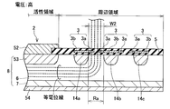
- FIGS. 1A and 1B are cross-sectional views of the semiconductor device 2 taken in the thickness direction.
- the semiconductor device 2 is a transistor in which a P-type body layer 53 is formed in an active region of a semiconductor substrate 8 in which an N ⁇ type drift layer 6 and an N + type collector layer 7 are stacked.
- illustration of a gate etc. is abbreviate
- the drift layer 6 is not hatched to represent the cross section for easy understanding of the drawing. In the subsequent drawings, the drift layer 6 is not hatched.
- the semiconductor device 2 includes three FLRs so as to surround the active region when viewed in plan.
- the FLR close to the active region is referred to as the first FLR 14a
- the furthest FLR is referred to as the third FLR 14c
- the intermediate FLR is referred to as the second FLR 14b.
- the three FLRs are expressed without distinction, they are referred to as FLR14.
- the peripheral region of the first main surface (the upper surface in the figure) of the semiconductor device is covered with an insulating layer 5.
- a semiconductor layer 3 is provided in the insulating layer 5 above each FLR 14.
- the semiconductor layer 3 has a low surface density region 3a that overlaps a range between two adjacent FLRs (inter-ring range Ra) and a high surface density region 3b that overlaps the FLR 14 in a plan view of the substrate.
- in plan view of the substrate means “in a direction crossing the substrate in the thickness direction”.
- above FLR 14 means a direction from FLR 14 toward insulating layer 5.
- the high surface density region 3b includes impurities at a surface density higher than the RESURF surface density
- the low surface density region 3A includes impurities at a surface density lower than the RESURF surface density.
- the impurity contained may be P-type or N-type, but the entire semiconductor layer has the same conductivity type.
- FIG. 1A shows equipotential lines when the voltage applied between the main electrodes is low
- FIG. 1B shows equipotential lines when the voltage applied between the main electrodes is high.
- the voltage between both the main electrodes is low (FIG. 1A)
- carriers exist in both the low surface density region 3a and the high surface density region 3b of the semiconductor layer 3, so that the entire semiconductor layer 3 becomes a conductor. Therefore, the low areal density region 3a is entirely equipotential with the high areal density region 3b.
- the electric field that continues from the depletion layer of the drift layer 6 does not spread to the low areal density region 3a, and an electric field is generated in the range W1 where the semiconductor layer 3 (semiconductor layer 3 including the low areal density region 3a) does not exist.
- the electric field continuing from the depletion layer of the drift layer 6 is generated only in the range W1 in the inter-ring range Ra.
- the range W1 is narrow, since the applied voltage is low, the electric field strength in the range W1 is also low, and dielectric breakdown does not occur.
- mobile ions can be trapped while carriers are present in the low areal density region 3a. Note that carriers always exist in the high areal density region 3b and trap mobile ions.
- a depletion layer is formed in the low areal density region 3a. If it does so, the low surface density area
- the range in which the electric field is generated in the inter-ring range Ra is expanded from W1 to W2, so that the increase in the electric field strength is mitigated.
- the depletion layer expands in the low areal density region 3a in the semiconductor layer 3 that overlaps the inter-ring range, that is, the insulating band expands, so that the increase in electric field strength is mitigated.
- a range W1 in FIG. 1A corresponds to a region that is always an insulating band.
- the same phenomenon occurs between the second FLR 14b and the third FLR 14c.
- a phenomenon similar to the phenomenon described above also occurs between the second FLR 14b and the third FLR 14c, and an increase in the electric field strength between the FLRs is mitigated.
- the surface density changes from the high surface density region 3b to the low surface density region 3a in a stepped manner.
- the impurity surface density gradually changes in one semiconductor layer, and is higher than the RESURF surface density in the range facing the FLR.
- the impurity surface density decreases as the end of the semiconductor layer 3 is approached. You may comprise so that it may be less than areal density. In such a configuration, the depletion layer in the semiconductor layer expands according to the voltage applied to the semiconductor device, and the increase in the electric field strength in the inter-ring range is mitigated.
- the above effect can also be constituted by a semiconductor layer containing impurities at a surface density lower than the RESURF surface density and another semiconductor layer containing impurities at a high surface density.
- said effect can also be comprised with the semiconductor layer and conductor layer which contain an impurity with the surface density lower than a RESURF surface density. That is, the above-described effects can be obtained even if the high areal density region 3b in FIGS. 1A and 1B is formed of a semiconductor layer independent of the low areal density region 3a.
- the same effect can be obtained by replacing the high areal density region 3b with a conductor.
- the following configuration is preferably provided.
- the conductor layer provided in the insulating layer faces one FLR (for example, the first FLR 14a in FIG. 1A) and surrounds the active region. Then, the edge in the width direction of the semiconductor layer extends to the edge in the width direction of the FLR (first FLR 14a) and the FLR adjacent to the edge in the width direction of the conductor layer (for example, the second FLR 14b in FIG. 1A). Yes.
- the semiconductor layer located between the end of the conductor layer and the adjacent FLR corresponds to the low areal density region 3a in FIGS. 1A and 1B.
- the conductor layer also traps mobile ions inside the insulating layer and prevents the insulating layer from deteriorating.
- the lower limit value of the impurity surface density in the low surface density region of the semiconductor layer is 1.0 ⁇ E ⁇ 6 [atoms / cm 2 ], which is generally defined as the boundary between the semiconductor and the nonconductor (insulator).
- the low areal density region needs to have such properties that carriers exist and the depletion layer expands when a certain voltage is applied.
- Various variations of the combination of the low areal density region, the high areal density region, and the conductor layer will be described in detail in Examples.
- the conductor layer may be a metal, but may be a layer in which polysilicon is excessively doped with impurities so as to be close to the conductor. Such a layer is also used for the gate of a semiconductor device. Therefore, the semiconductor layer in the insulating layer described above can be simultaneously formed by a conventional process for manufacturing a semiconductor device without increasing a special process for manufacturing the layer. Specifically, the conductor layer can be formed simultaneously with the step of forming a gate on the substrate. Further, the polysilicon layer serving as the base of the semiconductor layer described above can be formed simultaneously in the step of forming the polysilicon layer serving as the base of the element for temperature detection on the substrate.
- the method for manufacturing the semiconductor device is also a novel manufacturing method disclosed in this specification.
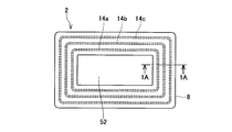
- FIG. 2 is a plan view of the semiconductor device 2.
- Reference numeral 52 denotes a first main electrode.
- the first main electrode 52 is one electrode of the transistor, and a region indicated by the first main electrode 52 in a plan view corresponds to an “active region”. In other words, the active region is a range occupied by the first main electrode 52 in a plan view of the substrate 8.
- an element transistor is formed in an active region.
- the periphery of the active region is the peripheral region.
- the semiconductor device 2 includes three FLRs (field limiting rings) in the peripheral region. Since the FLR is covered with the insulating layer 5 (see FIG. 1A), the FLR is indicated by a broken line in FIG. For easy understanding, FLR is shown in gray in FIG. As described above, in plan view, the first FLR 14a, the second FLR 14b, and the third FLR 14c are referred to from the inside.
- the plurality of FLRs 14 surround the active region in plan view.
- the FLR 14 is formed in the substrate, and the upper surface thereof is covered with the insulating layer 5.
- the semiconductor layer 3 is formed in the insulating layer 5 along each FLR. Therefore, although not illustrated in FIG. 2, each of the three semiconductor layers 3 also surrounds the active region in plan view.
- FIG. 3 is a cross-sectional view of the semiconductor device 2 at another position.
- the semiconductor layer 3 corresponding to each FLR is electrically connected to each FLR 14 by a conductor 13.
- the conductor 13 does not go around the active region in a plan view, and connects the FLR 14 and the semiconductor layer 3 in some places.
- the semiconductor layer 3 corresponding to each FLR and each FLR 14 are equipotential. Therefore, no electric field is generated between each FLR 14 and the semiconductor layer 3 located above each FLR. Accordingly, as shown in FIGS. 1A and 1B, the electric field region continuing from the depletion layer of the drift layer 6 passes between adjacent FLRs (first FLR 14a and second FLR 14b).
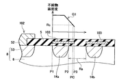
- FIG. 4 is an enlarged cross-sectional view of the semiconductor device 102 having a semiconductor layer whose surface density gradually changes.
- FIG. 5 is an enlarged cross-sectional view of a semiconductor device 202 having a semiconductor layer with another surface density distribution. 4 and 5 are enlarged views of the vicinity of two FLRs (first FLR 14a and second FLR 14b). 4 and 5 are the same as the semiconductor device 2 in FIG. 1A.
- FIG. 4 shows an areal density graph G1 on one semiconductor layer 103.
- the vertical axis of the surface density graph G ⁇ b> 1 indicates the surface density of impurities contained in the semiconductor layer 103, and the horizontal axis indicates the position in the semiconductor layer 103.
- the position P1 is an inner end of the semiconductor layer 103, and the position P3 is an outer end.
- the side closer to the active region corresponds to “inner side”, and the side far from the active region corresponds to “outer side”.
- the range of the first main electrode 52 corresponds to the active region.
- the position P1 also corresponds to the inner edge of the first FLR 14a.
- the position P2 corresponds to the outer edge of the first FLR 14a.
- the semiconductor layer 103 faces the first FLR 14a and extends to the inter-ring range Ra outside the first FLR 14a.
- the semiconductor layer 103 has a high impurity surface density on the inner side, and the surface density decreases toward the outer side.
- the symbol Rc indicates the RESURF surface density.
- the symbol Pc is a position where the impurity surface density corresponds to the RESURF surface density Rc.
- the region where the impurity surface density is higher than the RESURF surface density exceeds the range facing the first FLR 14a.
- the impurity surface density is lower than the RESURF surface density Rc in the inter-ring range Ra. In other words, the position Pc is located between the position P2 and the position P3.
- FIG. 5 shows an example of the semiconductor layer 203 having another surface density distribution.
- the semiconductor layer 203 of the semiconductor device 202 also has an impurity surface density distribution that gradually decreases from the inside toward the outside.
- the position Pc corresponding to the RESURF surface density Rc is located in a range facing the first FLR 14a.
- the semiconductor layer 103 of the semiconductor device 102 in FIG. 4 the low surface density region where the impurity surface density contained is lower than the RESURF surface density Rc is narrow, and in the semiconductor layer 203 of the semiconductor device 202 in FIG. Wide density range.
- the semiconductor device 102 has a smaller withstand voltage improvement effect than the semiconductor device 202, but has a larger mobile ion trap effect.
- the semiconductor device 202 has a greater breakdown voltage improvement effect and a smaller movable ion trap effect than the semiconductor device 102.
- the impurity surface density gradually decreases from the inside to the outside, but has a region (high surface density region) exceeding the RESURF surface density Rc in the range facing the FLR, The end portion has a region lower than the RESURF surface density Rc (low surface density region).
- the semiconductor layer may have a high areal density region and a low areal density region that change in a stepped manner.
- the surface density may gradually change in the surface density region.
- the semiconductor layer only needs to have a high surface density region in a part of the range facing the FLR, and the impurity surface density does not need to exceed the RESURF surface density in the entire range facing the FLR.
- the semiconductor layer only needs to have a low areal density region at the end of the range overlapping with the inter-ring range, and need not have a low areal density in the entire overlapping range.
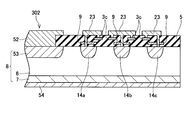
- the semiconductor device 302 includes a semiconductor layer 3c having a constant surface density and a conductor layer 9 inside the insulating layer 5 instead of a semiconductor layer whose surface density changes.
- a semiconductor layer 3c and a conductor layer 9 are provided for each FLR.
- Each conductor layer 9 faces each FLR.
- each conductor layer 9 surrounds the active region along each FLR.
- the semiconductor layer 3 c partially overlaps the conductor layer 9 and the FLR 14 in plan view of the substrate 8. Another part of the semiconductor layer 3 c overlaps the inter-ring range Ra adjacent to the FLR 14. In other words, the semiconductor layer 3c is closer to the adjacent FLR (for example, the second FLR 14b) than the corresponding edge of the FLR (for example, the first FLR 14a) and the edge of the corresponding conductor layer 9 in the width direction. It is growing.
- FIG. 6A shows equipotential lines passing through the depletion layer when a low voltage is applied between the main electrodes 52 and 54, as in FIG. 1A.
- FIG. 6B shows a high voltage as in FIG. 1B.
- 2 shows an equipotential line passing through the depletion layer.
- the semiconductor layer 3c contains impurities at a surface density lower than the RESURF surface density. Therefore, when a high voltage is applied, the depletion layer expands.
- the width of the depletion layer depends on the voltage. When the voltage is low, the depletion layer is narrow. When the voltage is extremely low, almost no depletion layer is generated in the semiconductor layer 3c (FIG. 6A). Therefore, carriers exist throughout the semiconductor layer 3c, and the entire semiconductor layer 3c is equipotential.
- the electric field continuing from the depletion layer generated in the drift layer 6 extends to the range W2 including the semiconductor layer 3c (but not including the conductor layer 9) in the inter-ring range Ra (FIG. 6B).
- the voltage is increased, the range in which the electric field is generated in the inter-ring range Ra is expanded, so that the electric field strength is relaxed and the breakdown voltage is improved.
- both the conductor layer 9 and the semiconductor layer 3c trap mobile ions.
- the voltage increases and the depletion layer spreads in the semiconductor layer 3c, only the conductor layer 9 traps mobile ions. If the voltage is low, mobile ions can be trapped in a large number of regions, and therefore deterioration of the insulating layer 5 due to mobile ions can be suppressed.
- FIG. 7 shows a cross-sectional view of the semiconductor device 302 at another position.
- each FLR 14 is electrically connected to the conductor layer 9 and the semiconductor layer 3 c corresponding to each FLR 14 through the electrode 23. That is, each FLR 14 and the conductor layer 9 and the semiconductor layer 3c corresponding to each FLR 14 have the same potential. Therefore, no electric field is generated between the FLR 14 and the conductor layer 9 or between the conductor layer 9 and the semiconductor layer 3c.
- the electric field continuing from the depletion layer of the drift layer 6 always passes through the range between adjacent FLRs (inter-ring range Ra).
- the electrode 23 may not surround the active region in plan view of the substrate 8.
- the electrode 23 only needs to conduct the FLR, the conductor layer, and the semiconductor layer around the active region. On the contrary, the electrode 23 may make a round so as to surround the active region in a plan view of the substrate.
- the target semiconductor device 402 is an IGBT (Insulated Gate Bipolar Transistor) with a diode for detecting the temperature of the element.
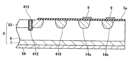
- FIG. 8A is a diagram illustrating a process of generating a gate. 8A, the N + type collector layer 7, the second main electrode 54 in contact with the collector layer 7, the P + type body layer 53, the gate trench 412, the first FLR 14a, The second FLR 14b and the temperature detection P + layer 419 are already formed. Since these layers can be manufactured by a conventional method, the description thereof is omitted.
- FIG. 8A shows a process of forming the gate 413.
- the gate 413 of the IGBT of the embodiment is obtained by filling the trench 412 with polysilicon.
- the polysilicon here has an impurity surface density sufficient to function as a conductor.
- the trench 412 is filled with polysilicon, and at the same time, the conductor layer 9 is formed above the first FLR 14a and the second FLR 24a with the same polysilicon.
- This conductor layer 9 is made of conductive polysilicon, which is the same as the gate.
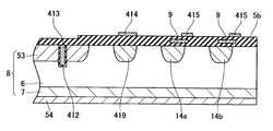
- an insulating layer is stacked on the main surface (insulating layer 5b).
- a polysilicon layer 414 serving as a base of a temperature detection diode and a poly-silicon serving as a base of a semiconductor layer are formed on the insulating layer 5b.
- a silicon layer 415 is formed (FIG. 8B).
- the polysilicon layer 414 serving as the base of the temperature detecting diode and the polysilicon layer 415 serving as the base of the semiconductor layer are formed of the same material.
- the polysilicon has N- conductivity type.
- a polysilicon layer 414 serving as a base of the temperature detection diode is formed above the temperature detection P + layer 419.
- the polysilicon layer 415 serving as the base of the semiconductor layer is formed so that a part thereof overlaps with each conductor layer 9.
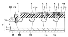
- the polysilicon layer 414 serving as the base of the semiconductor layer is formed simultaneously with the formation of the polysilicon layer 414 serving as the base of the temperature detecting element on the substrate 8.
- the polysilicon layer 414 is doped with P-type impurities, and the other half is doped with N-type impurities. As a result, the polysilicon layer 414 becomes a diode 414a.
- the polysilicon layer 415 serving as a base of the semiconductor layer is doped with an impurity having a desired surface density. For example, similarly to the semiconductor layer 303 of the semiconductor device 302 shown in FIG. 6A, the P-type impurity is doped so that the surface density is lower than the RESURF surface density. As a result, the polysilicon layer 415 becomes the semiconductor layer 3.
- a groove indicated by a symbol E in FIG. 8C indicates a portion where the insulating layer 5b is removed by etching.
- the insulating layer 5b is removed so that a part of the diode 414a is exposed, and the insulating layer 5b is exposed so that a part of the FLR 14, a part of the conductor layer 9, and a part of the semiconductor layer 3 are exposed. Corresponding parts are removed.
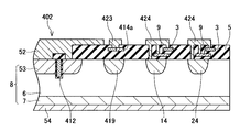
- the conductive polysilicon layer constitutes the first main electrode 52, the temperature detection diode electrode 423, and the FLR electrode 424.
- the FLR electrode 424 electrically connects the FLR (first FLR 14 and second FLR 24), the corresponding conductor layer 9, and the semiconductor layer 3 to each other.
- the above manufacturing method generates the conductor layer 9 and the semiconductor layer 3 using an existing process in an IGBT with the temperature detection diode 414a. Therefore, it is not necessary to add a new process for forming the conductor layer 9 and the semiconductor layer 3.
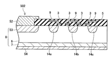
- a semiconductor device 502 of the third embodiment will be described with reference to FIG.
- This semiconductor device 502 has a structure close to that of the semiconductor device 302 of the second embodiment described above.
- the conductor layer 9 is provided near the FLR 14, and the semiconductor layer 3 is provided above the conductor layer 9.
- the semiconductor layer 3 is provided near the FLR 14, and the conductor layer 9 is provided above the semiconductor layer 3. That is, in the semiconductor devices 302 and 502, the positions of the conductor layer 9 and the semiconductor layer 3 in the vertical direction are reversed.
- the semiconductor device 502 has the same advantages as the semiconductor device 302.
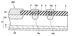
- each trench is filled with a conductor.
- the filled conductor corresponds to the electrode 23 a that conducts between the FLR 14 and the conductor layer 9.
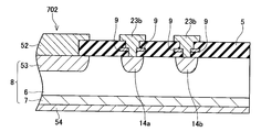
- a thick trench that penetrates the conductor layer 9 and reaches the FLR 14 is formed.
- the trench is filled with a conductor.
- the filled conductor corresponds to the electrode 23b.
- the conductor layer 9 is in contact with the side surface of the electrode 23b, and the FLR 14 is in contact with the lower surface of the electrode 23b.
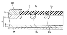
- the conductor layer 9a whose central portion is bent downward is formed.
- the bent portion of the conductor layer 9a is in contact with the FLR 14.
- the semiconductor device 802 has an advantage that an electrode for conducting the conductor layer 9a and the FLR 14 is unnecessary.
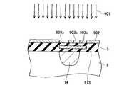
- a resist layer 902 is formed on the upper surface of the insulating layer 5 including the semiconductor layer 913 therein. A part of the resist layer is removed, and a plurality of openings (openings 903a, 903b, and 903c) from which the semiconductor layer 3 is exposed are formed. The width of the opening is adjusted according to the desired distribution of the impurity surface density.
- the widest opening 903a is provided corresponding to the region where the impurity is desired to be applied with the highest surface density
- the narrowest opening 903c is provided corresponding to the region where the impurity is desired to be provided with the lowest surface density.
- An opening 903b having an intermediate width is provided for a region where an impurity is desired to be supplied with an intermediate surface density.
- a P-type or N-type impurity 901 is doped.
- the semiconductor layer 3 having an impurity surface density corresponding to the size of the opening is obtained.
- a semiconductor layer having a high impurity surface density at the left end and a lower impurity surface density toward the right is obtained.
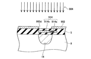
- doping is performed using an element having a small diffusion coefficient.
- elements having a small diffusion coefficient include arsenic (As), antimony (Sb), and indium (In).
- a resist layer 902 is formed on the upper surface of the insulating layer 5 including the semiconductor layer 914 therein. Then, the resist layer above the region where the impurity is desired to be applied at a high surface density is removed, and an opening 903d is formed. Thus, the element 904 having a small diffusion coefficient is doped. In the region where the impurity is directly implanted, a region (high surface density region 914b) containing the impurity at a high surface density is generated.
- the impurity used has a small diffusion coefficient, the impurity diffuses inside the semiconductor layer 914 from the high surface density region 914 b to a region where the impurity does not reach by the resist 902.
- an arrow drawn inside the semiconductor layer 914 represents impurity diffusion. In this manner, the region covered with the resist 902 becomes the low areal density region 914a.
- the semiconductor layer 3 corresponding to FLR14 and FLR14 and the conductor layer 9 corresponding to FLR14 are electrically connected to each other. It is preferable that the electrode that conducts the FLR 14 and the semiconductor layer 3 and the electrode that conducts the FLR and the conductor layer 9 wrap around the active region together with the FLR in a plan view of the substrate.
Landscapes
- Electrodes Of Semiconductors (AREA)
Abstract
Description
Claims (6)
- 基板の平面視において、素子が形成されている活性領域を囲んでいる複数のフィールドリミティングリングと、
半導体装置の主面上に設けられており、複数のフィールドリミティングリングを覆っている絶縁層と、
絶縁層内に設けられており、フィールドリミティングリングと平行に活性領域を囲んでいる半導体層と、
を備えており、
半導体層は、リサーフ条件の面密度よりも低い面密度で不純物を含んでいるとともに、平面視において、隣接するフィールドリミティングリングの間の範囲(リング間範囲)の一部とオーバーラップしており、リング間範囲の残部とオーバーラップしていないことを特徴とする半導体装置。 - 平面視において、半導体層は、
一つのフィールドリミティングリングと対向するとともに、一つのフィールドリミティングリングに隣接するリング間範囲の上方まで伸びており、
平面視において、リング間範囲内に位置する端部に、リサーフ条件の面密度よりも低い面密度で不純物を含む低面密度領域を有するとともに、一つのフィールドリミティングリングと対向する部分に、リサーフ条件の面密度よりも高い面密度で不純物を含む高面密度領域を有する、ことを特徴とする請求項1に記載の半導体装置。 - 半導体層が前記一つのフィールドリミティングリングと導通していることを特徴とする請求項2に記載の半導体装置。
- 絶縁層内に形成されており、一つのフィールドリミティングリングに対向するとともに活性領域を囲んでいる導体層をさらに備えており、
半導体層が、前記一つのフィールドリミティングリングの幅方向の縁、及び、導体層の幅方向の縁よりも隣接するフィールドリミティングリングの近くまで伸びている、
ことを特徴とする請求項1に記載の半導体装置。 - 半導体層と導体層と一つのフィールドリミティングリングが導通していることを特徴とする請求項4に記載の半導体装置。
- 請求項4又は5に記載の半導体装置の製造方法であり、
基板にトレンチゲートを形成するのと同時に前記導体層を形成する工程と、
基板に温度検出用の素子のベースとなるポリシリコン層を形成するのと同時に半導体層のベースとなるポリシリコン層を形成する工程と、
を含むことを特徴とする半導体装置の製造方法。
Priority Applications (5)
| Application Number | Priority Date | Filing Date | Title |
|---|---|---|---|
| JP2015500062A JP5888465B2 (ja) | 2013-02-15 | 2013-02-15 | 半導体装置とその製造方法 |
| US14/766,307 US9412809B2 (en) | 2013-02-15 | 2013-02-15 | Semiconductor device and manufacturing method thereof |
| DE112013006681.5T DE112013006681B4 (de) | 2013-02-15 | 2013-02-15 | Halbleitervorrichtung |
| CN201380072943.9A CN104995736B (zh) | 2013-02-15 | 2013-02-15 | 半导体装置及其制造方法 |
| PCT/JP2013/053724 WO2014125626A1 (ja) | 2013-02-15 | 2013-02-15 | 半導体装置とその製造方法 |
Applications Claiming Priority (1)
| Application Number | Priority Date | Filing Date | Title |
|---|---|---|---|
| PCT/JP2013/053724 WO2014125626A1 (ja) | 2013-02-15 | 2013-02-15 | 半導体装置とその製造方法 |
Publications (1)
| Publication Number | Publication Date |
|---|---|
| WO2014125626A1 true WO2014125626A1 (ja) | 2014-08-21 |
Family
ID=51353652
Family Applications (1)
| Application Number | Title | Priority Date | Filing Date |
|---|---|---|---|
| PCT/JP2013/053724 Ceased WO2014125626A1 (ja) | 2013-02-15 | 2013-02-15 | 半導体装置とその製造方法 |
Country Status (5)
| Country | Link |
|---|---|
| US (1) | US9412809B2 (ja) |
| JP (1) | JP5888465B2 (ja) |
| CN (1) | CN104995736B (ja) |
| DE (1) | DE112013006681B4 (ja) |
| WO (1) | WO2014125626A1 (ja) |
Cited By (4)
| Publication number | Priority date | Publication date | Assignee | Title |
|---|---|---|---|---|
| WO2016121968A1 (ja) * | 2015-01-29 | 2016-08-04 | 富士電機株式会社 | 半導体装置 |
| CN106206700A (zh) * | 2015-05-27 | 2016-12-07 | 丰田自动车株式会社 | 半导体装置 |
| US10985241B2 (en) | 2016-10-21 | 2021-04-20 | Toyota Jidosha Kabushiki Kaisha | Semiconductor device and production method thereof |
| JP2025506148A (ja) * | 2022-02-10 | 2025-03-07 | ヴィシャイ シリコニックス,エルエルシー | 高効率かつ高強度の高電圧シリコンカーバイドパワーデバイスを対象とした設計による適応エッジ終端 |
Families Citing this family (7)
| Publication number | Priority date | Publication date | Assignee | Title |
|---|---|---|---|---|
| JP6834156B2 (ja) * | 2016-03-16 | 2021-02-24 | 富士電機株式会社 | 半導体装置および製造方法 |
| JP2018186142A (ja) * | 2017-04-25 | 2018-11-22 | 株式会社村田製作所 | 半導体装置 |
| JP7268330B2 (ja) * | 2018-11-05 | 2023-05-08 | 富士電機株式会社 | 半導体装置および製造方法 |
| JP7608226B2 (ja) | 2021-03-19 | 2025-01-06 | 株式会社東芝 | 半導体装置 |
| WO2025044170A1 (zh) * | 2023-08-31 | 2025-03-06 | 海信家电集团股份有限公司 | 半导体装置 |
| CN118522764A (zh) * | 2023-09-28 | 2024-08-20 | 海信家电集团股份有限公司 | 半导体装置 |
| CN117116974B (zh) * | 2023-08-31 | 2024-08-16 | 海信家电集团股份有限公司 | 半导体装置 |
Citations (5)
| Publication number | Priority date | Publication date | Assignee | Title |
|---|---|---|---|---|
| JPH11330496A (ja) * | 1998-05-07 | 1999-11-30 | Hitachi Ltd | 半導体装置 |
| JP2001217420A (ja) * | 2000-02-01 | 2001-08-10 | Mitsubishi Electric Corp | 半導体装置 |
| JP2005093550A (ja) * | 2003-09-12 | 2005-04-07 | Toshiba Corp | 半導体装置 |
| JP2007123570A (ja) * | 2005-10-28 | 2007-05-17 | Toyota Industries Corp | 半導体装置 |
| JP2013012568A (ja) * | 2011-06-29 | 2013-01-17 | Mitsubishi Electric Corp | 半導体装置およびその製造方法 |
Family Cites Families (14)
| Publication number | Priority date | Publication date | Assignee | Title |
|---|---|---|---|---|
| JP2812093B2 (ja) * | 1992-09-17 | 1998-10-15 | 株式会社日立製作所 | プレーナ接合を有する半導体装置 |
| JP2850694B2 (ja) * | 1993-03-10 | 1999-01-27 | 株式会社日立製作所 | 高耐圧プレーナ型半導体装置 |
| JP2000114549A (ja) | 1998-09-30 | 2000-04-21 | Meidensha Corp | 半導体素子 |
| JP2002231944A (ja) * | 2001-01-31 | 2002-08-16 | Sanken Electric Co Ltd | 電力用半導体装置 |
| JP4264316B2 (ja) * | 2003-09-01 | 2009-05-13 | 株式会社豊田中央研究所 | 半導体装置とその製造方法 |
| JP5196766B2 (ja) * | 2006-11-20 | 2013-05-15 | 株式会社東芝 | 半導体装置 |
| JP4375439B2 (ja) * | 2007-05-30 | 2009-12-02 | 株式会社デンソー | ジャンクションバリアショットキーダイオードを備えた炭化珪素半導体装置 |
| JP2009117715A (ja) | 2007-11-08 | 2009-05-28 | Toshiba Corp | 半導体装置及びその製造方法 |
| JP5477681B2 (ja) * | 2008-07-29 | 2014-04-23 | 三菱電機株式会社 | 半導体装置 |
| JP5543758B2 (ja) * | 2009-11-19 | 2014-07-09 | ルネサスエレクトロニクス株式会社 | 半導体装置 |
| US8373224B2 (en) * | 2009-12-28 | 2013-02-12 | Force Mos Technology Co., Ltd. | Super-junction trench MOSFET with resurf stepped oxides and trenched contacts |
| US8278710B2 (en) * | 2010-07-23 | 2012-10-02 | Freescale Semiconductor, Inc. | Guard ring integrated LDMOS |
| JP5772987B2 (ja) | 2012-01-12 | 2015-09-02 | トヨタ自動車株式会社 | 半導体装置とその製造方法 |
| JP5686203B2 (ja) * | 2012-03-22 | 2015-03-18 | トヨタ自動車株式会社 | 半導体装置 |
-
2013
- 2013-02-15 US US14/766,307 patent/US9412809B2/en active Active
- 2013-02-15 DE DE112013006681.5T patent/DE112013006681B4/de active Active
- 2013-02-15 JP JP2015500062A patent/JP5888465B2/ja active Active
- 2013-02-15 CN CN201380072943.9A patent/CN104995736B/zh active Active
- 2013-02-15 WO PCT/JP2013/053724 patent/WO2014125626A1/ja not_active Ceased
Patent Citations (5)
| Publication number | Priority date | Publication date | Assignee | Title |
|---|---|---|---|---|
| JPH11330496A (ja) * | 1998-05-07 | 1999-11-30 | Hitachi Ltd | 半導体装置 |
| JP2001217420A (ja) * | 2000-02-01 | 2001-08-10 | Mitsubishi Electric Corp | 半導体装置 |
| JP2005093550A (ja) * | 2003-09-12 | 2005-04-07 | Toshiba Corp | 半導体装置 |
| JP2007123570A (ja) * | 2005-10-28 | 2007-05-17 | Toyota Industries Corp | 半導体装置 |
| JP2013012568A (ja) * | 2011-06-29 | 2013-01-17 | Mitsubishi Electric Corp | 半導体装置およびその製造方法 |
Cited By (9)
| Publication number | Priority date | Publication date | Assignee | Title |
|---|---|---|---|---|
| WO2016121968A1 (ja) * | 2015-01-29 | 2016-08-04 | 富士電機株式会社 | 半導体装置 |
| CN106489208A (zh) * | 2015-01-29 | 2017-03-08 | 富士电机株式会社 | 半导体装置 |
| JPWO2016121968A1 (ja) * | 2015-01-29 | 2017-04-27 | 富士電機株式会社 | 半導体装置 |
| US10304948B2 (en) | 2015-01-29 | 2019-05-28 | Fuji Electric Co., Ltd. | Semiconductor device |
| CN106206700A (zh) * | 2015-05-27 | 2016-12-07 | 丰田自动车株式会社 | 半导体装置 |
| JP2016225363A (ja) * | 2015-05-27 | 2016-12-28 | トヨタ自動車株式会社 | 半導体装置 |
| DE102016109641B4 (de) | 2015-05-27 | 2021-11-11 | Denso Corporation | Halbleitergerät |
| US10985241B2 (en) | 2016-10-21 | 2021-04-20 | Toyota Jidosha Kabushiki Kaisha | Semiconductor device and production method thereof |
| JP2025506148A (ja) * | 2022-02-10 | 2025-03-07 | ヴィシャイ シリコニックス,エルエルシー | 高効率かつ高強度の高電圧シリコンカーバイドパワーデバイスを対象とした設計による適応エッジ終端 |
Also Published As
| Publication number | Publication date |
|---|---|
| JPWO2014125626A1 (ja) | 2017-02-02 |
| US20150364541A1 (en) | 2015-12-17 |
| CN104995736B (zh) | 2018-03-30 |
| CN104995736A (zh) | 2015-10-21 |
| US9412809B2 (en) | 2016-08-09 |
| DE112013006681T5 (de) | 2015-10-29 |
| JP5888465B2 (ja) | 2016-03-22 |
| DE112013006681B4 (de) | 2022-01-20 |
Similar Documents
| Publication | Publication Date | Title |
|---|---|---|
| JP5888465B2 (ja) | 半導体装置とその製造方法 | |
| US9576841B2 (en) | Semiconductor device and manufacturing method | |
| JP5472309B2 (ja) | 半導体装置 | |
| US20130334598A1 (en) | Semiconductor device and method for manufacturing same | |
| JP5136578B2 (ja) | 半導体装置 | |
| JP6640691B2 (ja) | 半導体装置及びその製造方法 | |
| JPWO2013105350A1 (ja) | 半導体装置とその製造方法 | |
| JP2009176772A (ja) | 半導体装置 | |
| US10374043B2 (en) | Semiconductor device | |
| JP7351086B2 (ja) | 絶縁ゲート型半導体装置及びその製造方法 | |
| US10204980B2 (en) | Semiconductor device and manufacturing method of the same | |
| JP7288827B2 (ja) | 半導体装置の製造方法 | |
| CN103187440A (zh) | 具有横向绝缘栅双极晶体管的半导体器件 | |
| US12328914B2 (en) | Buried grid with shield in wide band gap material | |
| JP2018006648A (ja) | 半導体装置 | |
| JP2018037577A (ja) | 半導体装置 | |
| JP6471811B2 (ja) | 半導体装置 | |
| JP2019176077A (ja) | 半導体装置 | |
| JP6299658B2 (ja) | 絶縁ゲート型スイッチング素子 | |
| CN117015857A (zh) | 半导体装置 | |
| TWI714683B (zh) | 具有超晶格結構的表面優化電晶體 | |
| JP6606819B2 (ja) | 半導体装置 | |
| JP2019160899A (ja) | 半導体装置および半導体装置の製造方法 | |
| CN105633148A (zh) | Mos型功率器件及其形成方法 |
Legal Events
| Date | Code | Title | Description |
|---|---|---|---|
| 121 | Ep: the epo has been informed by wipo that ep was designated in this application |
Ref document number: 13875296 Country of ref document: EP Kind code of ref document: A1 |
|
| ENP | Entry into the national phase |
Ref document number: 2015500062 Country of ref document: JP Kind code of ref document: A |
|
| WWE | Wipo information: entry into national phase |
Ref document number: 14766307 Country of ref document: US |
|
| WWE | Wipo information: entry into national phase |
Ref document number: 112013006681 Country of ref document: DE Ref document number: 1120130066815 Country of ref document: DE |
|
| 122 | Ep: pct application non-entry in european phase |
Ref document number: 13875296 Country of ref document: EP Kind code of ref document: A1 |