WO2014115484A1 - Esd保護素子を有する半導体装置 - Google Patents
Esd保護素子を有する半導体装置 Download PDFInfo
- Publication number
- WO2014115484A1 WO2014115484A1 PCT/JP2013/085191 JP2013085191W WO2014115484A1 WO 2014115484 A1 WO2014115484 A1 WO 2014115484A1 JP 2013085191 W JP2013085191 W JP 2013085191W WO 2014115484 A1 WO2014115484 A1 WO 2014115484A1
- Authority
- WO
- WIPO (PCT)
- Prior art keywords
- diffusion layer
- type diffusion
- protection element
- esd protection
- semiconductor device
- Prior art date
- Legal status (The legal status is an assumption and is not a legal conclusion. Google has not performed a legal analysis and makes no representation as to the accuracy of the status listed.)
- Ceased
Links
Images



Classifications
-
- H—ELECTRICITY
- H10—SEMICONDUCTOR DEVICES; ELECTRIC SOLID-STATE DEVICES NOT OTHERWISE PROVIDED FOR
- H10D—INORGANIC ELECTRIC SEMICONDUCTOR DEVICES
- H10D84/00—Integrated devices formed in or on semiconductor substrates that comprise only semiconducting layers, e.g. on Si wafers or on GaAs-on-Si wafers
- H10D84/201—Integrated devices formed in or on semiconductor substrates that comprise only semiconducting layers, e.g. on Si wafers or on GaAs-on-Si wafers characterised by the integration of only components covered by H10D1/00 or H10D8/00, e.g. RLC circuits
- H10D84/204—Integrated devices formed in or on semiconductor substrates that comprise only semiconducting layers, e.g. on Si wafers or on GaAs-on-Si wafers characterised by the integration of only components covered by H10D1/00 or H10D8/00, e.g. RLC circuits of combinations of diodes or capacitors or resistors
- H10D84/221—Integrated devices formed in or on semiconductor substrates that comprise only semiconducting layers, e.g. on Si wafers or on GaAs-on-Si wafers characterised by the integration of only components covered by H10D1/00 or H10D8/00, e.g. RLC circuits of combinations of diodes or capacitors or resistors of only diodes
-
- H—ELECTRICITY
- H10—SEMICONDUCTOR DEVICES; ELECTRIC SOLID-STATE DEVICES NOT OTHERWISE PROVIDED FOR
- H10D—INORGANIC ELECTRIC SEMICONDUCTOR DEVICES
- H10D8/00—Diodes
- H10D8/411—PN diodes having planar bodies
-
- H—ELECTRICITY
- H10—SEMICONDUCTOR DEVICES; ELECTRIC SOLID-STATE DEVICES NOT OTHERWISE PROVIDED FOR
- H10D—INORGANIC ELECTRIC SEMICONDUCTOR DEVICES
- H10D89/00—Aspects of integrated devices not covered by groups H10D84/00 - H10D88/00
- H10D89/60—Integrated devices comprising arrangements for electrical or thermal protection, e.g. protection circuits against electrostatic discharge [ESD]
- H10D89/601—Integrated devices comprising arrangements for electrical or thermal protection, e.g. protection circuits against electrostatic discharge [ESD] for devices having insulated gate electrodes, e.g. for IGFETs or IGBTs
- H10D89/611—Integrated devices comprising arrangements for electrical or thermal protection, e.g. protection circuits against electrostatic discharge [ESD] for devices having insulated gate electrodes, e.g. for IGFETs or IGBTs using diodes as protective elements
Definitions
- the present invention relates to a semiconductor device, and more particularly to an ESD (electrostatic discharge) protection element mounted on a semiconductor device.
- ESD electrostatic discharge
- FIG. 6 is a sectional view and an equivalent circuit diagram showing a conventional ESD protection element.
- the surge voltage applied to the input pad is transmitted to the cathode electrode 106 connected to the input pad, and an ESD surge current flows from the input pad to the ground pad via the anode electrode 107.
- the Zener diode 108 (comprising the Zener region 103, the cathode 104, and the anode 105) and the Zener diode 109 (comprising the Zener region 103, the cathode 104, the substrate 101, and the pickup region 102) of the ESD protection element are:
- This ESD surge current flows in the reverse direction of the diode by the breakdown operation. Thereby, since the ESD surge current does not flow to the internal circuit, the internal circuit is protected from the ESD surge current (see, for example, Patent Document 1).
- the present invention provides a semiconductor device having an ESD protection element, which functions as a semiconductor substrate and cathodes of first to second Zener diodes and is formed on the surface of the semiconductor substrate.
- a first P-type diffusion layer that functions as an anode of the diffusion layer and the first Zener diode, and is formed on the surface of the N-type diffusion layer at a connection portion between the input pad and the input terminal of the ESD protection element;
- a second P-type diffusion layer which functions as an anode of the second Zener diode and is formed on the surface of the N-type diffusion layer at a connection portion between the ground pad and the ground terminal of the ESD protection element; and the first P-type diffusion In the region where the contact is provided on the layer, the first high-concentration P-type diffusion layer formed on the surface of the first P-type diffusion layer and the contact on the second P-type diffusion layer
- a semiconductor device having a ESD protection device characterized by comprising: a second
- the first Zener diode of the ESD protection element in the reverse connection state in which the power supply voltage is erroneously applied to the ground pad, the first Zener diode of the ESD protection element is reverse biased and thus turned off. Therefore, the power supply voltage applied to the ground pad is not applied to the input pad, so that the semiconductor device does not malfunction or be destroyed.
- P or N represents the conductivity type of the semiconductor region
- +, ⁇ , and ⁇ indicate the relative magnitude relationship of the impurity concentration, and the concentration increases in the order of P ⁇ , P ⁇ , and P +.
- FIG. 1 is a cross-sectional view and an equivalent circuit diagram showing an ESD protection element.
- FIG. 2 is a plan view showing the ESD protection element.
- a P-type well 12 is formed on the surface of a P-type semiconductor substrate 11 in a region where the ESD protection element 10 is not formed.
- an N-type well 13 is formed on the surface of the P-type semiconductor substrate 11.
- An N-type diffusion layer 14 is formed on the surface of the N-type well 13.
- a first P-type diffusion layer 15 a is formed on the surface of the N-type diffusion layer 14 at a connection portion between the input pad 31 and the input terminal of the ESD protection element 10.
- a second P-type diffusion layer 15 b is formed on the surface of the N-type diffusion layer 14 at a connection portion between the ground pad and the ground terminal of the ESD protection element 10.
- the surface of the P-type semiconductor substrate 11 is subjected to a LOCOS method (Local A relatively thick LOCOS oxide film 16 is formed by Oxidation of Silicon (a method of partially oxidizing silicon).
- LOCOS method Local A relatively thick LOCOS oxide film 16 is formed by Oxidation of Silicon (a method of partially oxidizing silicon).
- a high concentration P-type diffusion layer 17 c is formed on the surface of the P-type well 12.
- the first high-concentration P-type diffusion layer 17a is formed on the surface of the P-type diffusion layer 15a.
- the second high-concentration P-type diffusion layer 17b is formed on the surface of the P-type diffusion layer 15b.
- the N-type diffusion layer 14 functions as the cathode of the Zener diodes 21-22.
- the P-type diffusion layer 15 a functions as the anode of the Zener diode 21.
- the P-type diffusion layer 15 b functions as the anode of the Zener diode 22.
- the Zener diode 21 and the Zener diode 22 constitute the ESD protection element 10.
- the impurity concentration of the N-type diffusion layer 14 is higher than the impurity concentration of the N-type well 13.
- the impurity concentration of the P-type diffusion layers 15a to 15b is higher than the impurity concentration of the P-type well 12, and lower than the impurity concentration of the high-concentration P-type diffusion layers 17a to 17c.
- the impurity concentrations of the N-type diffusion layer 14 and the P-type diffusion layers 15a to 15b are appropriately designed according to the breakdown voltage of the Zener diodes 21 to 22. Further, the impurity concentration of the high-concentration P-type diffusion layers 17a to 17c is appropriately designed so that the value of the contact resistance between the high-concentration P-type diffusion layers 17a to 17c and the contact thereon is small.
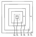
- the planar shapes of the P-type diffusion layer 15a and the high-concentration P-type diffusion layer 17a are squares with high symmetry in this embodiment.
- the LOCOS oxide film 16 and the high-concentration P-type diffusion layers 17b to 17c are formed symmetrically vertically and horizontally in the plan view of FIG.
- the input pad 31 is connected to the anode of the Zener diode 21 and the internal circuit of the semiconductor device.
- the cathode of the Zener diode 21 is connected to the cathode of the Zener diode 22.
- the anode of the Zener diode 22 is connected to the ground pad.
- the Zener diode 22 of the ESD protection element 10 is turned off because it is reverse-biased. Therefore, the ESD protection element 10 does not affect the voltage applied to the input pad 31.
- the ESD protection element 10 performs the reverse connection protection operation. That is, the Zener diode 21 of the ESD protection element 10 is reverse-biased and thus remains off. Therefore, the power supply voltage applied to the ground pad is not applied to the input pad 31.
- the ESD surge current flows from the input pad 31 to the ground pad due to the surge voltage applied to the input pad 31.
- the Zener diode 21 of the ESD protection element 10 passes this ESD surge current in the forward direction.
- the Zener diode 22 of the ESD protection element 10 allows this ESD surge current to flow in the reverse direction by the breakdown operation. Thereby, since the ESD surge current does not flow to the internal circuit, the internal circuit is protected from the ESD surge current.
- planar shapes of the P-type diffusion layer 15a and the high-concentration P-type diffusion layer 17a are squares, but may be octagons with corners cut to prevent electric field concentration.
- the LOCOS oxide film 16 and the high-concentration P-type diffusion layers 17b to 17c are formed symmetrically in the plan view with the P-type diffusion layer 15a and the high-concentration P-type diffusion layer 17a as the center.
- the LOCOS method is used, the STI method (Shallow : Trench Isolation: separation method using shallow grooves) may be used.
- planar shapes of the P-type diffusion layer 15a and the high-concentration P-type diffusion layer 17a may be rectangular.
- planar shapes of the P-type diffusion layer 15a and the high-concentration P-type diffusion layer 17a may be circular so as to avoid electric field concentration.
- the planar shape of the P-type diffusion layer 15a and the high-concentration P-type diffusion layer 17a may be a rectangle-like shape, and the rectangular portion in the short direction is rounded.
- the N-type well 13 may be omitted.
- the N-type diffusion layer 14 is formed directly on the surface of the P-type semiconductor substrate 11 in the region where the ESD protection element 10 is formed.
- ESD protection element 11 P-type semiconductor substrate 12 P-type well 13 N-type well 14 N-type diffusion layer (cathode of Zener diodes 21 to 22) 15a P-type diffusion layer (anode of Zener diode 21) 15b P-type diffusion layer (anode of Zener diode 22) 16 LOCOS oxide films 17a to 17c High-concentration P-type diffusion layer 18 N-type diffusion layer 21 Zener diode 22 Zener diode 31 Input pad
Landscapes
- Semiconductor Integrated Circuits (AREA)
- Metal-Oxide And Bipolar Metal-Oxide Semiconductor Integrated Circuits (AREA)
Abstract
逆接続保護機能を有するESD保護素子を有する半導体装置とするために、半導体装置は、ツェナーダイオード21および22のカソードとして機能する半導体基板11の表面に形成されるN型拡散層14と、入力パッド31とESD保護素子10の入力端子との接続部分において、N型拡散層14の表面に形成される、ツェナーダイオード21のアノードとして機能するP型拡散層15aと、接地パッドとESD保護素子10の接地端子との接続部分において、N型拡散層14の表面に形成される、ツェナーダイオード22のアノードとして機能するP型拡散層15bとを備えたESD保護素子を有する。
Description
本発明は、半導体装置に関する、特に、半導体装置に搭載されるESD(静電気放電)保護素子に関する。
従来のESD保護素子について説明する。図6は、従来のESD保護素子を示す断面図及び等価回路図である。
入力パッドに印加されたサージ電圧は、入力パッドに連なるカソード電極106へ伝わり、ESDサージ電流が入力パッドから接地パッドにアノード電極107を介して流れる。この時、ESD保護素子のツェナーダイオード108(ツェナー領域103、カソード104、及び、アノード105からなる)及びツェナーダイオード109(ツェナー領域103、カソード104、及び、基板101、ピックアップ領域102からなる)は、ブレイクダウン動作により、このESDサージ電流をダイオードの逆方向に流す。これにより、ESDサージ電流は内部回路に流れないので、内部回路がESDサージ電流から保護されることになる(例えば、特許文献1参照)。
しかし、特許文献1によって開示された技術では、電源電圧が接地パッドに誤って印加される逆接続の状態においては、ダイオードが順方向となり接地パッドから入力パッドへと電流が流れてしまう。そのため、半導体装置は、誤動作したり破壊されたりしてしまう可能性が高い。そこで、製品によってはこうした事態を避けるために、半導体装置に搭載されるESD保護素子には、逆接続保護機能が要求されるようになる。本発明は、上記課題に鑑みてなされ、逆接続保護機能を有するESD保護素子を備えた半導体装置を提供するものである。
本発明は、上記課題を解決するため、ESD保護素子を有する半導体装置であって、半導体基板と、第一~第二ツェナーダイオードのカソードとして機能し、前記半導体基板の表面に形成されるN型拡散層と、前記第一ツェナーダイオードのアノードとして機能し、入力パッドとESD保護素子の入力端子との接続部分において、前記N型拡散層の表面に形成される第一P型拡散層と、前記第二ツェナーダイオードのアノードとして機能し、接地パッドとESD保護素子の接地端子との接続部分において、前記N型拡散層の表面に形成される第二P型拡散層と、前記第一P型拡散層の上にコンタクトが設けられる領域において、前記第一P型拡散層の表面に形成される第一高濃度P型拡散層と、前記第二P型拡散層の上にコンタクトが設けられる領域において、前記第二P型拡散層の表面に形成される第二高濃度P型拡散層と、を備えることを特徴とするESD保護素子を有す半導体装置提供する。
本発明では、電源電圧が接地パッドに誤って印加される逆接続の状態において、ESD保護素子の第一ツェナーダイオードは、逆バイアスとなるので、オフしている。そのため、接地パッドに印加された電源電圧は、入力パッドに印加されないので、半導体装置は、誤動作したり破壊されたりしない。
以下、本発明の実施形態について、図面を参照して説明する。図中のPあるいはNは半導体領域の導電型を表し、付属する+、±、-は不純物濃度の相対的な大小関係を示し、P-、P±、P+の順で濃度は高くなる。N型に関しても同様である。
まず、半導体装置におけるESD(静電気放電)保護素子の構成について説明する。図1は、ESD保護素子を示す断面図及び等価回路図である。図2は、ESD保護素子を示す平面図である。
図1の(A)に示すように、ESD保護素子10が形成されない領域において、P型半導体基板11の表面に、P型ウェル12が形成されている。ESD保護素子10が形成される領域において、P型半導体基板11の表面に、N型ウェル13が形成されている。N型ウェル13の表面には、N型拡散層14が形成されている。そして、入力パッド31とESD保護素子10の入力端子との接続部分には、N型拡散層14の表面に、第一のP型拡散層15aが形成されている。さらに、接地パッドとESD保護素子10の接地端子との接続部分において、N型拡散層14の表面に、第二のP型拡散層15bが形成されている。
P型ウェル12及びP型拡散層15a~15bの上にコンタクトをとるための高濃度P型拡散層17a~17cが設けられない領域において、P型半導体基板11の表面には、LOCOS法(Local Oxidation of Silicon:シリコンを部分的に酸化する方法)による比較的膜厚の厚いLOCOS酸化膜16が形成されている。P型ウェル12の上にコンタクトが設けられる領域において、P型ウェル12の表面に、高濃度P型拡散層17cが形成される。P型拡散層15aの上にコンタクトが設けられる領域において、P型拡散層15aの表面に、第一の高濃度P型拡散層17aが形成される。P型拡散層15bの上にコンタクトが設けられる領域において、P型拡散層15bの表面に、第二の高濃度P型拡散層17bが形成される。
N型拡散層14は、ツェナーダイオード21~22のカソードとして機能する。P型拡散層15aは、ツェナーダイオード21のアノードとして機能する。P型拡散層15bは、ツェナーダイオード22のアノードとして機能する。ツェナーダイオード21及びツェナーダイオード22がESD保護素子10を構成している。
N型拡散層14の不純物濃度は、N型ウェル13の不純物濃度よりも濃い。P型拡散層15a~15bの不純物濃度は、P型ウェル12の不純物濃度よりも濃く、高濃度P型拡散層17a~17cの不純物濃度よりも薄い。N型拡散層14及びP型拡散層15a~15bの不純物濃度は、ツェナーダイオード21~22の耐圧によって適宜設計される。また、高濃度P型拡散層17a~17cの不純物濃度は、高濃度P型拡散層17a~17cとその上のコンタクトとの接触抵抗の値が小さくなるよう適宜設計される。
また、図2に示すように、P型拡散層15a及び高濃度P型拡散層17aの平面形状は、本実施形態においては、対称性の高い正方形である。これらのP型拡散層15a及び高濃度P型拡散層17aを中心として、図2の平面図で上下左右対称に、LOCOS酸化膜16及び高濃度P型拡散層17b~17cを形成する。
次に、ESD保護素子10の回路について説明する。
図1の(B)に示すように、入力パッド31は、ツェナーダイオード21のアノード及び半導体装置の内部回路に接続される。ツェナーダイオード21のカソードは、ツェナーダイオード22のカソードに接続される。ツェナーダイオード22のアノードは、接地パッドに接続される。
次に、ESD保護素子10の動作について説明する。
通常の動作においてはESD保護素子10のツェナーダイオード22は、逆バイアスとなるので、オフしている。よって、ESD保護素子10は、入力パッド31に印加される電圧に影響しない。
次に、電源電圧が接地パッドに誤って印加される逆接続の状態においては、ESD保護素子10は逆接続保護動作を行う。即ち、ESD保護素子10のツェナーダイオード21は、逆バイアスとなるので、オフしたままである。よって、接地パッドに印加された電源電圧は、入力パッド31に印加されない。
続いて、ESD保護素子10のESD保護動作について説明する。
入力パッド31へ印加されたサージ電圧により、ESDサージ電流が入力パッド31から接地パッドに流れる。この時、ESD保護素子10のツェナーダイオード21は、このESDサージ電流を順方向に流している。また、ESD保護素子10のツェナーダイオード22は、ブレイクダウン動作により、このESDサージ電流を逆方向に流している。これにより、ESDサージ電流が内部回路に流れないので、内部回路がESDサージ電流から保護される。
なお、P型拡散層15a及び高濃度P型拡散層17aの平面形状は、正方形であるが、電界集中防止のため、角をカットされた八角形としても良い。この時、これらのP型拡散層15a及び高濃度P型拡散層17aを中心として、平面図で上下左右対称に、LOCOS酸化膜16及び高濃度P型拡散層17b~17cを形成する。
また、LOCOS法が使用されているが、STI法(Shallow Trench Isolation:浅い溝を使った分離方法)を使用しても良い。
また、図3に示すように、P型拡散層15a及び高濃度P型拡散層17aの平面形状は、長方形としても良い。
また、図4に示すように、P型拡散層15a及び高濃度P型拡散層17aの平面形状は、電界の集中を避けられるように円形としても良い。
また、図5に示すように、P型拡散層15a及び高濃度P型拡散層17aの平面形状は、長方形類似の形状でも良く、この長方形の短手方向の部分は、丸くなっている。
また、N型ウェル13は、無くても良い。この時、ESD保護素子10が形成される領域において、P型半導体基板11の表面に、直接、N型拡散層14が形成される。
10 ESD保護素子
11 P型半導体基板
12 P型ウェル
13 N型ウェル
14 N型拡散層(ツェナーダイオード21~22のカソード)
15a P型拡散層(ツェナーダイオード21のアノード)
15b P型拡散層(ツェナーダイオード22のアノード)
16 LOCOS酸化膜
17a~17c 高濃度P型拡散層
18 N型拡散層
21 ツェナーダイオード
22 ツェナーダイオード
31 入力パッド
11 P型半導体基板
12 P型ウェル
13 N型ウェル
14 N型拡散層(ツェナーダイオード21~22のカソード)
15a P型拡散層(ツェナーダイオード21のアノード)
15b P型拡散層(ツェナーダイオード22のアノード)
16 LOCOS酸化膜
17a~17c 高濃度P型拡散層
18 N型拡散層
21 ツェナーダイオード
22 ツェナーダイオード
31 入力パッド
Claims (8)
- P型の半導体基板と、
第一のツェナーダイオードおよび第二のツェナーダイオードのカソードとして機能し、前記半導体基板の表面から内部にかけて形成されたN型拡散層と、
前記第一のツェナーダイオードのアノードとして機能し、入力パッドとESD保護素子の入力端子との接続部分において、前記N型拡散層の表面に形成された第一のP型拡散層と、
前記第二のツェナーダイオードのアノードとして機能し、接地パッドとESD保護素子の接地端子との接続部分において、前記N型拡散層の表面に形成された第二のP型拡散層と、
前記第一のP型拡散層の上にコンタクトが設けられる領域において、前記第一のP型拡散層の表面に形成された第一の高濃度P型拡散層と、
前記第二のP型拡散層の上にコンタクトが設けられる領域において、前記第二のP型拡散層の表面に形成された第二の高濃度P型拡散層と、
を備えたことを特徴とするESD保護素子を有する半導体装置。 - 前記N型拡散層の下に、さらに、N型のウェルを有することを特徴とする請求項1記載のESD保護素子を有する半導体装置。
- 前記ESD保護素子は周囲には、さらに、P型ウェルを有し、前記P型ウェルは第三の高濃度P型拡散層を介して前記接地パッドに接続されていることを特徴とする請求項1または2に記載のESD保護素子を有する半導体装置。
- 前記第一のP型拡散層の平面形状は、正方形である、
ことを特徴とする請求項1乃至3のいずれか1項に記載のESD保護素子を有する半導体装置。 - 前記第一のP型拡散層の平面形状は、長方形である、
ことを特徴とする請求項1乃至3のいずれか1項に記載のESD保護素子を有する半導体装置。 - 前記第一のP型拡散層の平面形状は、八角形である、
ことを特徴とする請求項1乃至3のいずれか1項に記載のESD保護素子を有する半導体装置。 - 前記第一のP型拡散層の平面形状は、円形である、
ことを特徴とする請求項1乃至3のいずれか1項に記載のESD保護素子を有する半導体装置。 - 前記第一のP型拡散層の平面形状は、長方形類似の形状であり、長方形の短手方向の部分は、丸くなっている、
ことを特徴とする請求項1乃至3のいずれか1項に記載のESD保護素子を有する半導体装置。
Applications Claiming Priority (2)
| Application Number | Priority Date | Filing Date | Title |
|---|---|---|---|
| JP2013-012388 | 2013-01-25 | ||
| JP2013012388A JP2014143378A (ja) | 2013-01-25 | 2013-01-25 | Esd保護素子を有する半導体装置 |
Publications (1)
| Publication Number | Publication Date |
|---|---|
| WO2014115484A1 true WO2014115484A1 (ja) | 2014-07-31 |
Family
ID=51227284
Family Applications (1)
| Application Number | Title | Priority Date | Filing Date |
|---|---|---|---|
| PCT/JP2013/085191 Ceased WO2014115484A1 (ja) | 2013-01-25 | 2013-12-27 | Esd保護素子を有する半導体装置 |
Country Status (3)
| Country | Link |
|---|---|
| JP (1) | JP2014143378A (ja) |
| TW (1) | TW201448158A (ja) |
| WO (1) | WO2014115484A1 (ja) |
Families Citing this family (1)
| Publication number | Priority date | Publication date | Assignee | Title |
|---|---|---|---|---|
| TW201640646A (zh) * | 2015-05-13 | 2016-11-16 | 台灣類比科技股份有限公司 | 積體電路的連接墊靜電防護元件 |
Citations (4)
| Publication number | Priority date | Publication date | Assignee | Title |
|---|---|---|---|---|
| JPH05218459A (ja) * | 1991-11-18 | 1993-08-27 | Sgs Thomson Microelectron Sa | モノリシック単方向保護ダイオード |
| JPH11259148A (ja) * | 1997-12-31 | 1999-09-24 | Siliconix Inc | 静電放電(esd)保護回路 |
| JP2006261376A (ja) * | 2005-03-17 | 2006-09-28 | Mitsubishi Electric Corp | ダイオード及び半導体装置 |
| JP2012182381A (ja) * | 2011-03-02 | 2012-09-20 | Panasonic Corp | 半導体装置 |
-
2013
- 2013-01-25 JP JP2013012388A patent/JP2014143378A/ja active Pending
- 2013-12-27 WO PCT/JP2013/085191 patent/WO2014115484A1/ja not_active Ceased
-
2014
- 2014-01-13 TW TW103101158A patent/TW201448158A/zh unknown
Patent Citations (4)
| Publication number | Priority date | Publication date | Assignee | Title |
|---|---|---|---|---|
| JPH05218459A (ja) * | 1991-11-18 | 1993-08-27 | Sgs Thomson Microelectron Sa | モノリシック単方向保護ダイオード |
| JPH11259148A (ja) * | 1997-12-31 | 1999-09-24 | Siliconix Inc | 静電放電(esd)保護回路 |
| JP2006261376A (ja) * | 2005-03-17 | 2006-09-28 | Mitsubishi Electric Corp | ダイオード及び半導体装置 |
| JP2012182381A (ja) * | 2011-03-02 | 2012-09-20 | Panasonic Corp | 半導体装置 |
Also Published As
| Publication number | Publication date |
|---|---|
| TW201448158A (zh) | 2014-12-16 |
| JP2014143378A (ja) | 2014-08-07 |
Similar Documents
| Publication | Publication Date | Title |
|---|---|---|
| US10978441B2 (en) | Transient voltage suppressor and method for manufacturing the same | |
| CN202839623U (zh) | 半导体器件 | |
| US9082620B1 (en) | Semiconductor device | |
| CN109256381B (zh) | 瞬时电压抑制装置 | |
| JP2013073992A (ja) | 半導体装置 | |
| JP4209432B2 (ja) | 静電破壊保護装置 | |
| JP2001257366A (ja) | 半導体装置 | |
| TW201318141A (zh) | 半導體裝置 | |
| CN102844863A (zh) | 用作静电放电保护措施的晶体管组件 | |
| JP2014067986A (ja) | 半導体装置 | |
| JP4209433B2 (ja) | 静電破壊保護装置 | |
| JP6007606B2 (ja) | 半導体装置 | |
| JP3902040B2 (ja) | 半導体保護装置 | |
| JP4017573B2 (ja) | ダイオード | |
| JP2008172165A (ja) | 半導体装置 | |
| TWI477018B (zh) | 暫態電壓抑制器電路與用於其中之二極體元件及其製造方法 | |
| JP2010021218A (ja) | 半導体装置 | |
| JP2008235612A (ja) | 保護素子 | |
| TWI575759B (zh) | 半導體裝置佈局結構 | |
| CN107301995A (zh) | 瞬态电压抑制器及其制作方法 | |
| JP2014143378A (ja) | Esd保護素子を有する半導体装置 | |
| JP6838504B2 (ja) | 半導体装置および半導体回路装置 | |
| JP2006005028A (ja) | 半導体保護装置 | |
| JP2014165317A (ja) | 半導体装置 | |
| KR100331857B1 (ko) | 정전기 보호회로 |
Legal Events
| Date | Code | Title | Description |
|---|---|---|---|
| 121 | Ep: the epo has been informed by wipo that ep was designated in this application |
Ref document number: 13872826 Country of ref document: EP Kind code of ref document: A1 |
|
| NENP | Non-entry into the national phase |
Ref country code: DE |
|
| 122 | Ep: pct application non-entry in european phase |
Ref document number: 13872826 Country of ref document: EP Kind code of ref document: A1 |