WO2014103706A1 - キャリア付銅箔、及び、それを用いたプリント配線板、プリント回路板及び銅張積層板 - Google Patents
キャリア付銅箔、及び、それを用いたプリント配線板、プリント回路板及び銅張積層板 Download PDFInfo
- Publication number
- WO2014103706A1 WO2014103706A1 PCT/JP2013/083108 JP2013083108W WO2014103706A1 WO 2014103706 A1 WO2014103706 A1 WO 2014103706A1 JP 2013083108 W JP2013083108 W JP 2013083108W WO 2014103706 A1 WO2014103706 A1 WO 2014103706A1
- Authority
- WO
- WIPO (PCT)
- Prior art keywords
- layer
- carrier
- copper foil
- copper
- less
- Prior art date
Links
Images


Classifications
-
- B—PERFORMING OPERATIONS; TRANSPORTING
- B32—LAYERED PRODUCTS
- B32B—LAYERED PRODUCTS, i.e. PRODUCTS BUILT-UP OF STRATA OF FLAT OR NON-FLAT, e.g. CELLULAR OR HONEYCOMB, FORM
- B32B15/00—Layered products comprising a layer of metal
- B32B15/01—Layered products comprising a layer of metal all layers being exclusively metallic
-
- B—PERFORMING OPERATIONS; TRANSPORTING
- B32—LAYERED PRODUCTS
- B32B—LAYERED PRODUCTS, i.e. PRODUCTS BUILT-UP OF STRATA OF FLAT OR NON-FLAT, e.g. CELLULAR OR HONEYCOMB, FORM
- B32B15/00—Layered products comprising a layer of metal
- B32B15/20—Layered products comprising a layer of metal comprising aluminium or copper
-
- H—ELECTRICITY
- H05—ELECTRIC TECHNIQUES NOT OTHERWISE PROVIDED FOR
- H05K—PRINTED CIRCUITS; CASINGS OR CONSTRUCTIONAL DETAILS OF ELECTRIC APPARATUS; MANUFACTURE OF ASSEMBLAGES OF ELECTRICAL COMPONENTS
- H05K1/00—Printed circuits
- H05K1/02—Details
- H05K1/09—Use of materials for the conductive, e.g. metallic pattern
-
- H—ELECTRICITY
- H05—ELECTRIC TECHNIQUES NOT OTHERWISE PROVIDED FOR
- H05K—PRINTED CIRCUITS; CASINGS OR CONSTRUCTIONAL DETAILS OF ELECTRIC APPARATUS; MANUFACTURE OF ASSEMBLAGES OF ELECTRICAL COMPONENTS
- H05K3/00—Apparatus or processes for manufacturing printed circuits
- H05K3/02—Apparatus or processes for manufacturing printed circuits in which the conductive material is applied to the surface of the insulating support and is thereafter removed from such areas of the surface which are not intended for current conducting or shielding
- H05K3/022—Processes for manufacturing precursors of printed circuits, i.e. copper-clad substrates
- H05K3/025—Processes for manufacturing precursors of printed circuits, i.e. copper-clad substrates by transfer of thin metal foil formed on a temporary carrier, e.g. peel-apart copper
-
- B—PERFORMING OPERATIONS; TRANSPORTING
- B32—LAYERED PRODUCTS
- B32B—LAYERED PRODUCTS, i.e. PRODUCTS BUILT-UP OF STRATA OF FLAT OR NON-FLAT, e.g. CELLULAR OR HONEYCOMB, FORM
- B32B2457/00—Electrical equipment
- B32B2457/08—PCBs, i.e. printed circuit boards
-
- H—ELECTRICITY
- H05—ELECTRIC TECHNIQUES NOT OTHERWISE PROVIDED FOR
- H05K—PRINTED CIRCUITS; CASINGS OR CONSTRUCTIONAL DETAILS OF ELECTRIC APPARATUS; MANUFACTURE OF ASSEMBLAGES OF ELECTRICAL COMPONENTS
- H05K1/00—Printed circuits
- H05K1/02—Details
- H05K1/0271—Arrangements for reducing stress or warp in rigid printed circuit boards, e.g. caused by loads, vibrations or differences in thermal expansion
-
- H—ELECTRICITY
- H05—ELECTRIC TECHNIQUES NOT OTHERWISE PROVIDED FOR
- H05K—PRINTED CIRCUITS; CASINGS OR CONSTRUCTIONAL DETAILS OF ELECTRIC APPARATUS; MANUFACTURE OF ASSEMBLAGES OF ELECTRICAL COMPONENTS
- H05K2201/00—Indexing scheme relating to printed circuits covered by H05K1/00
- H05K2201/03—Conductive materials
- H05K2201/0332—Structure of the conductor
- H05K2201/0335—Layered conductors or foils
- H05K2201/0355—Metal foils
-
- H—ELECTRICITY
- H05—ELECTRIC TECHNIQUES NOT OTHERWISE PROVIDED FOR
- H05K—PRINTED CIRCUITS; CASINGS OR CONSTRUCTIONAL DETAILS OF ELECTRIC APPARATUS; MANUFACTURE OF ASSEMBLAGES OF ELECTRICAL COMPONENTS
- H05K2201/00—Indexing scheme relating to printed circuits covered by H05K1/00
- H05K2201/09—Shape and layout
- H05K2201/09009—Substrate related
- H05K2201/09136—Means for correcting warpage
-
- H—ELECTRICITY
- H05—ELECTRIC TECHNIQUES NOT OTHERWISE PROVIDED FOR
- H05K—PRINTED CIRCUITS; CASINGS OR CONSTRUCTIONAL DETAILS OF ELECTRIC APPARATUS; MANUFACTURE OF ASSEMBLAGES OF ELECTRICAL COMPONENTS
- H05K3/00—Apparatus or processes for manufacturing printed circuits
- H05K3/38—Improvement of the adhesion between the insulating substrate and the metal
- H05K3/389—Improvement of the adhesion between the insulating substrate and the metal by the use of a coupling agent, e.g. silane
Definitions
- the present invention relates to a copper foil with a carrier, and a printed wiring board, a printed circuit board and a copper clad laminate using the same.
- a printed wiring board is manufactured as a copper clad laminate in which an insulating substrate mainly composed of a copper foil and a glass epoxy substrate, a BT resin, a polyimide film or the like is bonded. Bonding is performed by laminating an insulating substrate and a copper foil and applying heat and pressure (lamination method), or by applying a varnish that is a precursor of an insulating substrate material to a surface having a coating layer of copper foil, A heating / curing method (casting method) is used.
- the thickness of the copper foil used for the copper clad laminate is also 9 ⁇ m, further 5 ⁇ m or less.
- the handleability when forming a copper clad laminate by the above-described lamination method or casting method is extremely deteriorated. Therefore, a copper foil with a carrier has appeared, in which a thick metal foil is used as a carrier, and an ultrathin copper layer is formed on the metal foil via a release layer.
- a general method of using the carrier-attached copper foil is to peel the carrier together with the release layer after bonding the surface of the ultrathin copper layer to an insulating substrate and thermocompression bonding.
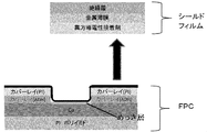
- FIG. 1 is a schematic diagram of a shield film formed using a carrier-attached copper foil and an FPC (flexible printed circuit board) including the shield film.
- FPC flexible printed circuit board
- each layer of PI (polyimide), Cu, and coverlay (polyimide with an adhesive (ADH)) is formed in this order, and a minute recess is formed in the coverlay.
- a plating layer is provided on Cu provided in the recess and is electrically connected to the shield film.
- a shield film is press-bonded to the surface of such an FPC. At this time, the shield film is embedded in the recess so as to be electrically connected to the wiring portion.
- the shield film is provided with a metal thin film and an anisotropic conductive adhesive on the insulating layer in this order, and is press-bonded to the FPC surface from the anisotropic conductive adhesive side.
- the metal thin film of this shield film corresponds to the ultrathin copper layer of the copper foil with carrier. That is, after preparing an insulating layer for the shield film and bonding the copper foil with a carrier on the surface from the ultrathin copper layer side, the copper foil carrier is peeled off from the ultrathin copper layer, and the copper foil carrier after peeling
- a shield film is formed by providing an anisotropic conductive adhesive on the surface of the thin copper layer.
- this invention makes it a subject to provide the copper foil with a carrier which can suppress favorably the peeling
- the present inventor has conducted extensive research, and by forming pinholes of a predetermined size with a predetermined number density in an ultrathin copper layer, the gas or vapor generated by heating or the like is generated. It has been found that a carrier-attached copper foil capable of satisfactorily suppressing the occurrence of FPC blistering due to remaining can be provided.
- the copper foil carrier, the intermediate layer, and the ultrathin copper layer are laminated with copper foil in this order, and the ultrathin copper layer has a diameter.
- the ultra-thin copper pinhole diameter is 1 ⁇ m or 50 ⁇ m or less in layer is present 100 / cm 2 or more 3000 / cm 2 or less.
- Another aspect of the present invention is a copper foil with a carrier in which a copper foil carrier, an intermediate layer, and an ultrathin copper layer are laminated in this order, and the ultrathin copper layer has a pinhole having a diameter of 5 ⁇ m or more and 10 ⁇ m or less. It is a copper foil with a carrier in which there are 3000 / cm 2 or less pinholes having a diameter of 100 / cm 2 or more and a diameter of 1 ⁇ m or more and 50 ⁇ m or less.
- a copper foil with a carrier in which a copper foil carrier, an intermediate layer, and an ultrathin copper layer are laminated in this order, and the pinhole having a diameter of 5 ⁇ m to 10 ⁇ m in the ultrathin copper layer.
- a copper foil with a carrier present at 100 / cm 2 or more and 1000 / cm 2 or less.
- the diameter ultra-thin copper layer is 10 ⁇ m or less pinholes than 5 ⁇ m exist 1000 / cm 2 or less.
- the ultra-thin copper 20 ⁇ m or less pinhole diameter is 1 ⁇ m or more layers are present 10 / cm 2 or more 1000 / cm 2 or less.
- the ultra-thin copper pinhole diameter is 5 ⁇ m or more 10 ⁇ m or less in layer is present 100 / cm 2 or more 1000 / cm 2 or less.
- the average roughness Rz-avg of the intermediate layer formed on the surface where the average roughness Rz-avg of the copper foil carrier exceeds 2 ⁇ m exceeds 2 ⁇ m.
- An ultrathin copper layer having a thickness of 3 ⁇ m or less is provided on the surface.
- the average roughness Rz-avg of the intermediate layer formed on the surface where the average roughness Rz-avg of the copper foil carrier exceeds 2 ⁇ m exceeds 2 ⁇ m.
- An ultrathin copper layer having a thickness of 2 ⁇ m or less is provided on the surface.
- the average roughness Rz-avg of the intermediate layer formed on the surface having an average roughness Rz-avg of the copper foil carrier of 2 ⁇ m or less is 2 ⁇ m or less.
- An ultrathin copper layer having a thickness of 2 ⁇ m or less is provided on the surface.
- the average roughness Rz-avg of the intermediate layer formed on the surface having an average roughness Rz-avg of the copper foil carrier of 2 ⁇ m or less is 2 ⁇ m or less.
- An ultrathin copper layer having a thickness of 1 ⁇ m or less is provided on the surface.
- the ultrathin copper layer has an average roughness Rz-avg on the surface opposite to the copper foil carrier of 1 ⁇ m or more and 4 ⁇ m or less.
- the average roughness Rz-avg of the surface on the copper foil carrier side of the layer is not less than the average roughness Rz-avg on the surface opposite to the copper foil carrier.
- the carrier-attached copper foil of the present invention has a roughened layer on the surface of the ultrathin copper layer.
- the carrier-attached copper foil of the present invention is one type selected from the group consisting of a heat-resistant layer, a rust-proof layer, a chromate-treated layer, and a silane coupling-treated layer on the surface of the roughened layer. It has the above layers.
- At least one of the rust prevention layer and the heat-resistant layer contains one or more elements selected from nickel, cobalt, copper, and zinc.
- At least one of the rust prevention layer and the heat-resistant layer is composed of one or more elements selected from nickel, cobalt, copper, and zinc.
- the copper foil with a carrier of the present invention has the heat-resistant layer on the roughening layer.
- the carrier-attached copper foil of the present invention has the rust-preventing layer on the roughening treatment layer or the heat-resistant layer.
- the copper foil with a carrier of the present invention has the chromate treatment layer on the rust prevention layer.
- the carrier-attached copper foil of the present invention has the silane coupling treatment layer on the chromate treatment layer.
- the carrier-attached copper foil of the present invention is one type selected from the group consisting of a heat-resistant layer, a rust-proof layer, a chromate treatment layer, and a silane coupling treatment layer on the surface of the ultrathin copper layer. It has the above layers.
- the copper foil with a carrier of the present invention comprises a resin layer on the ultrathin copper layer.
- the copper foil with a carrier of the present invention includes a resin layer on the roughening treatment layer.
- the carrier-attached copper foil of the present invention is a resin layer on one or more layers selected from the group consisting of the heat-resistant layer, the rust-proof layer, the chromate-treated layer, and the silane coupling-treated layer. Is provided.
- the resin layer includes a dielectric.
- the present invention is a copper-clad laminate manufactured using the carrier-attached copper foil of the present invention.
- the present invention is a printed wiring board manufactured using the copper foil with a carrier of the present invention.
- the present invention is a printed circuit board manufactured using the copper foil with a carrier of the present invention.
- a step of preparing the carrier-attached copper foil of the present invention and an insulating substrate Laminating the copper foil with carrier and an insulating substrate; After laminating the copper foil with carrier and the insulating substrate, a copper clad laminate is formed through a step of peeling the copper foil carrier of the copper foil with carrier, Thereafter, the printed wiring board manufacturing method includes a step of forming a circuit by any one of a semi-additive method, a subtractive method, a partly additive method, or a modified semi-additive method.
- a step of forming a circuit on the ultrathin copper layer side surface of the copper foil with a carrier of the present invention Forming a resin layer on the ultrathin copper layer side surface of the carrier-attached copper foil so that the circuit is buried; Forming a circuit on the resin layer; Forming the circuit on the resin layer, and then peeling the carrier; and After the carrier is peeled off, the printed wiring board includes a step of exposing the circuit embedded in the resin layer formed on the surface of the ultrathin copper layer by removing the ultrathin copper layer Is the method.
- the step of forming a circuit on the resin layer is performed by laminating another copper foil with a carrier on the resin layer from the ultrathin copper layer side.
- the circuit is formed using a copper foil with a carrier bonded to a layer.
- another copper foil with a carrier to be bonded onto the resin layer is the copper foil with a carrier of the present invention.
- the step of forming a circuit on the resin layer is any one of a semi-additive method, a subtractive method, a partly additive method, or a modified semi-additive method. Done by the method.
- the printed wiring board manufacturing method of the present invention further includes a step of forming a substrate on the carrier-side surface of the carrier-attached copper foil before peeling off the carrier.
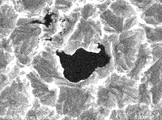
- FIG. 1 It is a schematic diagram which shows the structural example of a shield film and FPC using the same. It is an optical microscope observation photograph of the copper foil carrier side surface of the ultra-thin copper layer after copper foil carrier peeling of Example 2.
- FIG. 2 It is a SEM observation photograph of the copper foil carrier side surface of the ultra-thin copper layer after copper foil carrier peeling of Example 2.
- FIG. 2 It is a SEM observation photograph of the surface on the opposite side to the copper foil carrier of the ultra-thin copper layer after peeling of the copper foil carrier of Example 2.
- FIG. 1 It is a schematic diagram which shows the structural example of a shield film and FPC using the same.
- FIG. 1 It is a SEM observation photograph of the copper foil carrier side surface of the ultra-thin copper layer after copper foil carrier peeling of Example 4.
- FIG. It is a SEM observation photograph of the surface on the opposite side to the copper foil carrier of the ultra-thin copper layer after peeling of the copper foil carrier of Example 4.
- FIGS. 8A to 8C are schematic views of a cross section of a wiring board in a process up to circuit plating and resist removal according to a specific example of a method of manufacturing a printed wiring board using the carrier-attached copper foil of the present invention.
- D to F are schematic views of the cross section of the wiring board in the process from the lamination of the resin and the second-layer copper foil with a carrier to the laser drilling according to a specific example of the method for manufacturing a printed wiring board using the copper foil with a carrier of the present invention.
- GI are schematic views of the cross section of the wiring board in the steps from via fill formation to first layer carrier peeling, according to a specific example of the method for producing a printed wiring board using the copper foil with carrier of the present invention.
- J to K are schematic views of a cross section of a wiring board in steps from flash etching to bump / copper pillar formation according to a specific example of a method of manufacturing a printed wiring board using the carrier-attached copper foil of
- the copper foil carrier that can be used in the present invention is typically provided in the form of a rolled copper foil or an electrolytic copper foil.
- the electrolytic copper foil is produced by electrolytic deposition of copper from a copper sulfate plating bath onto a drum of titanium or stainless steel, and the rolled copper foil is produced by repeating plastic working and heat treatment with a rolling roll.
- the copper foil material is, for example, Sn-containing copper, Ag-containing copper, copper alloy added with Cr, Zr, Mg, etc., and Corson-based added with Ni, Si, etc. Copper alloys such as copper alloys can also be used.
- a copper alloy foil is also included.
- the thickness of the copper foil carrier that can be used in the present invention is not particularly limited, but may be appropriately adjusted to a thickness suitable for serving as a carrier, for example, 12 ⁇ m or more. However, if it is too thick, the production cost becomes high, so generally it is preferably 35 ⁇ m or less. Accordingly, the thickness of the copper foil carrier is typically 12-70 ⁇ m, more typically 18-35 ⁇ m.
- An intermediate layer is provided on one or both sides of the copper foil carrier. Another layer may be provided between the copper foil carrier and the intermediate layer.
- the ultrathin copper layer is hardly peeled off from the carrier before the copper foil with the carrier is laminated on the insulating substrate, while the ultrathin copper layer is separated from the carrier after the lamination step on the insulating substrate. There is no particular limitation as long as it can be peeled off.
- the intermediate layer of the copper foil with a carrier of the present invention is Cr, Ni, Co, Fe, Mo, Ti, W, P, Cu, Al, Zn, alloys thereof, hydrates thereof, oxides thereof, One or two or more selected from the group consisting of organic substances may be included.
- the intermediate layer may be a plurality of layers.
- the intermediate layer is a single metal layer composed of one kind of element selected from the element group composed of Cr, Ni, Co, Fe, Mo, Ti, W, P, Cu, Al, Zn from the carrier side.
- an alloy layer composed of one or more elements selected from the group consisting of Cr, Ni, Co, Fe, Mo, Ti, W, P, Cu, Al, Zn, From hydrates or oxides or organic substances of one or more elements selected from the group consisting of Cr, Ni, Co, Fe, Mo, Ti, W, P, Cu, Al, Zn It can comprise by forming the layer which becomes.
- the intermediate layer is a single metal layer composed of one kind of element selected from the element group composed of Cr, Ni, Co, Fe, Mo, Ti, W, P, Cu, Al, Zn from the carrier side.
- an alloy layer composed of one or more elements selected from the group consisting of Cr, Ni, Co, Fe, Mo, Ti, W, P, Cu, Al, Zn
- a single metal layer made of one element selected from the group consisting of Cr, Ni, Co, Fe, Mo, Ti, W, P, Cu, Al, Zn, or Cr, Ni, Co , Fe, Mo, Ti, W, P, Cu, Al, and Zn can be formed by forming an alloy layer made of one or more elements selected from the group of elements.
- a rust prevention layer such as a Ni plating layer on the opposite side of the copper foil carrier.
- the intermediate layer When the intermediate layer is provided by chromate treatment, zinc chromate treatment, or plating treatment, it is considered that some of the attached metal such as chromium and zinc may be hydrates or oxides.
- the intermediate layer can be formed by laminating nickel, a nickel-phosphorus alloy or a nickel-cobalt alloy, and chromium in this order on a copper foil carrier. Since the adhesive strength between nickel and copper is higher than the adhesive strength between chromium and copper, when the ultrathin copper layer is peeled off, it peels at the interface between the ultrathin copper layer and chromium. Further, the nickel of the intermediate layer is expected to have a barrier effect that prevents the copper component from diffusing from the carrier into the ultrathin copper layer.
- Adhesion amount of nickel in the intermediate layer is preferably 100 [mu] g / dm 2 or more 40000 ⁇ g / dm 2 or less, more preferably 100 [mu] g / dm 2 or more 4000 ⁇ g / dm 2 or less, more preferably 100 [mu] g / dm 2 or more 2500 g / dm 2 or less, more Preferably, it is 100 ⁇ g / dm 2 or more and less than 1000 ⁇ g / dm 2 , and the amount of chromium deposited on the intermediate layer is preferably 5 ⁇ g / dm 2 or more and 100 ⁇ g / dm 2 or less.
- a rust prevention layer such as a Ni plating layer on the opposite side of the copper foil carrier.
- Ultrathin copper layer is provided on the intermediate layer. Another layer may be provided between the intermediate layer and the ultrathin copper layer.
- Ultrathin copper layer of the present invention diameter is 50 ⁇ m or less pinholes than 1 ⁇ m exist 3000 / cm 2 or less 1 / cm 2 or more.
- the copper foil is formed on the copper foil carrier by electrolysis, there is no problem of handling, and the thinner the thickness, the more pinholes can be obtained.
- the roughness of the copper foil carrier is also S surface (shiny surface), M Since any surface (mat surface) can be used, the size and number of pinholes can be easily changed. In the case of a conventional deposited film of several hundreds of nanometers, the presence of a large number of pinholes can discharge the gas generated from the FPC at the time of solder reflow, but when this is replaced with copper foil, Since it is necessary to consider the followability to the hole, a thin copper foil with a hole is required. This is a feature that cannot be achieved with rolled copper foil.
- Ultrathin copper layer of the present invention diameter 20 ⁇ m or less pinholes than 1 ⁇ m is 10 / cm 2 or more 1000 / cm 2 is preferably present less in diameter is 10 ⁇ m or less pinholes than 5 [mu] m 100 pieces / more preferably there cm 2 or more 1000 / cm 2 or less.
- the ultra thin copper layer may be provided on both sides of the carrier.
- the ultra-thin copper layer can be formed by electroplating using an electrolytic bath such as copper sulfate, copper pyrophosphate, copper sulfamate, copper cyanide, etc., and is used in general electrolytic copper foil with high current density. Since a copper foil can be formed, a copper sulfate bath is preferable.
- an ultrathin copper layer by electrolysis on a copper foil carrier, there are no handling problems, and the thinner the copper layer, the more pinholes can be formed.
- the size and number density of pinholes can be easily controlled by utilizing the roughness of the surface of the S surface (shiny surface) and M surface (matte surface) of the copper foil carrier.
- the thickness of the ultrathin copper layer is not particularly limited, but is generally thinner than the carrier, for example, 12 ⁇ m or less. Typically, it can be 0.5-12 ⁇ m, more typically 1-5 ⁇ m, and even more typically 1-3 ⁇ m. In addition, when the thickness of an ultra-thin copper layer is 5 micrometers or less, there exists an advantage that an ultra-thin copper layer tends to follow the shape of the FPC surface.
- a roughening treatment layer may be provided on the surface of the ultrathin copper layer by performing a roughening treatment, for example, in order to improve the adhesion to the insulating substrate.
- the roughening treatment can be performed, for example, by forming roughened particles with copper or a copper alloy.
- the roughening process may be fine.
- the roughening treatment layer is a single layer selected from the group consisting of copper, nickel, phosphorus, tungsten, arsenic, molybdenum, chromium, cobalt and zinc, or a layer made of an alloy containing one or more of them. Also good.
- a roughening treatment can be performed in which secondary particles or tertiary particles are further formed of nickel, cobalt, copper, zinc alone or an alloy.
- a heat-resistant layer or a rust-preventing layer may be formed of nickel, cobalt, copper, zinc alone or an alloy, and the surface thereof may be further subjected to a treatment such as a chromate treatment or a silane coupling treatment.
- a heat-resistant layer or a rust-preventing layer may be formed from nickel, cobalt, copper, zinc alone or an alloy without roughening, and the surface may be subjected to a treatment such as chromate treatment or silane coupling treatment. Good.
- one or more layers selected from the group consisting of a heat-resistant layer, a rust-preventing layer, a chromate treatment layer, and a silane coupling treatment layer may be formed on the surface of the roughening treatment layer.
- One or more layers selected from the group consisting of a heat-resistant layer, a rust prevention layer, a chromate treatment layer, and a silane coupling treatment layer may be formed on the surface.
- the above-mentioned heat-resistant layer, rust prevention layer, chromate treatment layer, and silane coupling treatment layer may each be formed of a plurality of layers (for example, 2 layers or more, 3 layers or more, etc.).
- a known heat-resistant layer can be used as the heat-resistant layer. Further, for example, the following surface treatment can be used.
- the heat-resistant layer and the rust-proof layer known heat-resistant layers and rust-proof layers can be used.
- the heat-resistant layer and / or the anticorrosive layer is a group of nickel, zinc, tin, cobalt, molybdenum, copper, tungsten, phosphorus, arsenic, chromium, vanadium, titanium, aluminum, gold, silver, platinum group elements, iron, tantalum
- it may be a metal layer or an alloy layer made of one or more elements selected from the group consisting of iron, tantalum and the like.
- the heat-resistant layer and / or rust preventive layer is a group of nickel, zinc, tin, cobalt, molybdenum, copper, tungsten, phosphorus, arsenic, chromium, vanadium, titanium, aluminum, gold, silver, platinum group elements, iron, and tantalum.
- An oxide, nitride, or silicide containing one or more elements selected from the above may be included.
- the heat-resistant layer and / or the rust preventive layer may be a layer containing a nickel-zinc alloy.
- the heat-resistant layer and / or the rust preventive layer may be a nickel-zinc alloy layer.
- the nickel-zinc alloy layer may contain 50 wt% to 99 wt% nickel and 50 wt% to 1 wt% zinc, excluding inevitable impurities.
- the total adhesion amount of zinc and nickel in the nickel-zinc alloy layer may be 5 to 1000 mg / m 2 , preferably 10 to 500 mg / m 2 , preferably 20 to 100 mg / m 2 .
- the amount of nickel deposited on the layer containing the nickel-zinc alloy or the nickel-zinc alloy layer is preferably 0.5 mg / m 2 to 500 mg / m 2 , and 1 mg / m 2 to 50 mg / m 2 . More preferably.
- the heat-resistant layer and / or rust prevention layer is a layer containing a nickel-zinc alloy, the interface between the copper foil and the resin substrate is eroded by the desmear liquid when the inner wall of a through hole or via hole comes into contact with the desmear liquid. It is difficult to improve the adhesion between the copper foil and the resin substrate.
- the rust prevention layer may be a chromate treatment layer. A known chromate treatment layer can be used for the chromate treatment layer.
- a chromate treatment layer refers to a layer treated with a liquid containing chromic anhydride, chromic acid, dichromic acid, chromate or dichromate.
- Chromate treatment layer is any element such as cobalt, iron, nickel, molybdenum, zinc, tantalum, copper, aluminum, phosphorus, tungsten, tin, arsenic and titanium (metal, alloy, oxide, nitride, sulfide, etc.) May be included).
- Specific examples of the chromate treatment layer include a pure chromate treatment layer and a zinc chromate treatment layer.
- a chromate treatment layer treated with an anhydrous chromic acid or potassium dichromate aqueous solution is referred to as a pure chromate treatment layer.
- a chromate treatment layer treated with a treatment liquid containing chromic anhydride or potassium dichromate and zinc is referred to as a zinc chromate treatment layer.
- the heat-resistant layer and / or the rust preventive layer has a nickel or nickel alloy layer with an adhesion amount of 1 mg / m 2 to 100 mg / m 2 , preferably 5 mg / m 2 to 50 mg / m 2 , and an adhesion amount of 1 mg / m 2.
- a tin layer of ⁇ 80 mg / m 2 , preferably 5 mg / m 2 ⁇ 40 mg / m 2 may be sequentially laminated.
- the nickel alloy layer may be nickel-molybdenum, nickel-zinc, nickel-molybdenum-cobalt. You may be comprised by any one of these.
- the heat-resistant layer and / or rust-preventing layer preferably has a total adhesion amount of nickel or nickel alloy and tin of 2 mg / m 2 to 150 mg / m 2 and 10 mg / m 2 to 70 mg / m 2 . It is more preferable.
- the carrier-clad copper foil is processed into a printed wiring board, and the subsequent circuit peeling strength, the chemical resistance deterioration rate of the peeling strength, and the like are improved.
- coating weight of cobalt 200 ⁇ 2000 ⁇ g / dm 2 of cobalt -50 ⁇ 700 [mu] g / dm 2 of nickel - can form a nickel alloy plating layer.
- This treatment can be regarded as a kind of rust prevention treatment in a broad sense.
- This cobalt-nickel alloy plating layer needs to be performed to such an extent that the adhesive strength between the copper foil and the substrate is not substantially lowered.
- the amount of cobalt adhesion is less than 200 ⁇ g / dm 2 , the heat-resistant peel strength is lowered, and the oxidation resistance and chemical resistance may be deteriorated. As another reason, if the amount of cobalt is small, the treated surface becomes reddish, which is not preferable.
- a known weathering layer can be used as the silane coupling treatment layer.
- a well-known silane coupling process layer can be used, for example, The silane coupling process layer formed using the following silanes can be used.
- the silane coupling agent used for the silane coupling treatment a known silane coupling agent may be used.
- an amino silane coupling agent, an epoxy silane coupling agent, or a mercapto silane coupling agent may be used.
- Silane coupling agents include vinyltrimethoxysilane, vinylphenyltrimethoxylane, ⁇ -methacryloxypropyltrimethoxysilane, ⁇ -glycidoxypropyltrimethoxysilane, 4-glycidylbutyltrimethoxysilane, and ⁇ -aminopropyl.
- Triethoxysilane N- ⁇ (aminoethyl) ⁇ -aminopropyltrimethoxysilane, N-3- (4- (3-aminopropoxy) ptoxy) propyl-3-aminopropyltrimethoxysilane, imidazolesilane, triazinesilane, ⁇ -mercaptopropyltrimethoxysilane or the like may be used.
- the silane coupling treatment layer may be formed using a silane coupling agent such as epoxy silane, amino silane, methacryloxy silane, mercapto silane, or the like.
- a silane coupling agent such as epoxy silane, amino silane, methacryloxy silane, mercapto silane, or the like.
- you may use 2 or more types of such silane coupling agents in mixture.
- it is preferable to form using an amino-type silane coupling agent or an epoxy-type silane coupling agent.
- the amino silane coupling agent referred to here is N- (2-aminoethyl) -3-aminopropyltrimethoxysilane, 3- (N-styrylmethyl-2-aminoethylamino) propyltrimethoxysilane, 3- Aminopropyltriethoxysilane, bis (2-hydroxyethyl) -3-aminopropyltriethoxysilane, aminopropyltrimethoxysilane, N-methylaminopropyltrimethoxysilane, N-phenylaminopropyltrimethoxysilane, N- (3 -Acryloxy-2-hydroxypropyl) -3-aminopropyltriethoxysilane, 4-aminobutyltriethoxysilane, (aminoethylaminomethyl) phenethyltrimethoxysilane, N- (2-aminoethyl-3-aminopropyl
- the silane coupling treatment layer is 0.05 mg / m 2 to 200 mg / m 2 , preferably 0.15 mg / m 2 to 20 mg / m 2 , preferably 0.3 mg / m 2 to 2.0 mg in terms of silicon atoms. / M 2 is desirable. In the case of the above-mentioned range, the adhesiveness between the base resin and the surface-treated copper foil can be further improved.
- the copper foil with a carrier of the present invention may include a roughening treatment layer on an ultrathin copper layer, and may include a heat-resistant layer and / or a rust prevention layer on the roughening treatment layer.
- a chromate treatment layer may be provided on the heat-resistant layer and / or the rust prevention layer, and a silane coupling treatment layer may be provided on the chromate treatment layer.
- the copper foil with a carrier of the present invention may include a heat-resistant layer and / or a rust-preventing layer on the ultrathin copper layer, and may include a chromate treatment layer on the heat-resistant layer and / or the rust-preventing layer.
- a silane coupling treatment layer may be provided on the chromate treatment layer.
- the carrier-attached copper foil includes a resin layer on the ultrathin copper layer, the roughened layer, the heat-resistant layer, the rust-proof layer, the chromate-treated layer, or the silane coupling-treated layer. May be.
- the resin layer may be an insulating resin layer.
- the order of forming the heat-resistant layer, the rust-proofing layer, the chromate-treated layer, and the silane coupling-treated layer is not limited to each other, and in any order on the ultrathin copper layer or the roughened layer. These layers may be formed.
- the resin layer may be an adhesive or an insulating resin layer in a semi-cured state (B stage state) for bonding.
- the semi-cured state (B stage state) is a state in which there is no sticky feeling even if the surface is touched with a finger, the insulating resin layer can be stacked and stored, and a curing reaction occurs when subjected to heat treatment. Including that.
- the resin layer may be an adhesive resin, that is, an adhesive, or may be a semi-cured (B-stage) insulating resin layer for adhesion.
- the semi-cured state (B stage state) is a state in which there is no sticky feeling even if the surface is touched with a finger, the insulating resin layer can be stacked and stored, and a curing reaction occurs when subjected to heat treatment. Including that.
- the resin layer may contain a thermosetting resin or a thermoplastic resin.
- the resin layer may include a thermoplastic resin.
- the resin layer may contain a known resin, resin curing agent, compound, curing accelerator, dielectric, reaction catalyst, crosslinking agent, polymer, prepreg, skeleton material, and the like.
- the resin layer may be, for example, International Publication No. WO2008 / 004399, International Publication No. WO2008 / 053878, International Publication No. WO2009 / 084533, JP-A-11-5828, JP-A-11-140281, Patent 3184485, International Publication No. WO 97/02728, Japanese Patent No. 3676375, Japanese Patent Laid-Open No. 2000-43188, Japanese Patent No.
- Japanese Patent Laid-Open No. 2002-179721 Japanese Patent Laid-Open No. 2002-359444, Japanese Patent Laid-Open No. 2003-302068, Japanese Patent No. 3992225, Japanese Patent Laid-Open No. 2003-2225 No. 249739, Japanese Patent No. 4136509, Japanese Patent Application Laid-Open No. 2004-82687, Japanese Patent No. 40251177, Japanese Patent Application Laid-Open No. 2004-349654, Japanese Patent No. 4286060, Japanese Patent Application Laid-Open No. 2005-262506, Japanese Patent No. 4570070, Japanese Patent Application Laid-Open No. -53218, Japanese Patent No. 3949676, Japanese Patent No.
- the type of the resin layer is not particularly limited.
- epoxy resin polyimide resin, polyfunctional cyanate ester compound, maleimide compound, polymaleimide compound, maleimide resin, aromatic maleimide resin , Polyvinyl acetal resin, urethane resin, acrylic resin, polyethersulfone (also referred to as polyethersulfone or polyethersulfone), polyethersulfone (also referred to as polyethersulfone or polyethersulfone) resin, aromatic polyamide resin , Aromatic polyamide resin polymer, rubber resin, polyamine, aromatic polyamine, polyamideimide resin, rubber modified epoxy resin, phenoxy resin, carboxyl group-modified acrylonitrile-butadiene resin, polyphenylene oxide, bismale Midtriazine resin, thermosetting polyphenylene oxide resin, cyanate ester resin, carboxylic acid anhydride, polyvalent carboxylic acid anhydride, linear polymer having crosslinkable functional group, polyphenylene ether resin, 2,2-bis
- the epoxy resin has two or more epoxy groups in the molecule and can be used without any problem as long as it can be used for electric / electronic materials.
- the epoxy resin is preferably an epoxy resin epoxidized using a compound having two or more glycidyl groups in the molecule.
- bisphenol A type epoxy resin bisphenol F type epoxy resin, bisphenol S type epoxy resin, bisphenol AD type epoxy resin, novolac type epoxy resin, cresol novolac type epoxy resin, alicyclic epoxy resin, brominated (brominated) epoxy Resin, phenol novolac type epoxy resin, naphthalene type epoxy resin, brominated bisphenol A type epoxy resin, orthocresol novolac type epoxy resin, rubber modified bisphenol A type epoxy resin, glycidylamine type epoxy resin, triglycidyl isocyanurate, N, N -Glycidylamine compounds such as diglycidyl aniline, glycidyl ester compounds such as diglycidyl tetrahydrophthalate, phosphorus-containing epoxy resins, biphenyl type epoxy resin , Biphenyl novolac type epoxy resin, trishydroxyphenylmethane type epoxy resin, tetraphenylethane type epoxy resin, or a mixture of two or more types, or a hydrogenated product
- the phosphorus-containing epoxy resin a known epoxy resin containing phosphorus can be used.
- the phosphorus-containing epoxy resin is, for example, an epoxy resin obtained as a derivative from 9,10-dihydro-9-oxa-10-phosphaphenanthrene-10-oxide having two or more epoxy groups in the molecule. Is preferred.
- the resin layer may include a dielectric (dielectric filler).
- a dielectric (dielectric filler) is included in any of the above resin layers or resin compositions, it can be used for the purpose of forming the capacitor layer and increase the capacitance of the capacitor circuit.
- the dielectric (dielectric filler) include BaTiO 3 , SrTiO 3 , Pb (Zr—Ti) O 3 (common name PZT), PbLaTiO 3 ⁇ PbLaZrO (common name PLZT), SrBi 2 Ta 2 O 9 (common name SBT), and the like.
- a composite oxide dielectric powder having a perovskite structure is used.
- the dielectric (dielectric filler) may be in powder form.
- the powder characteristics of the dielectric (dielectric filler) are such that the particle size is in the range of 0.01 ⁇ m to 3.0 ⁇ m, preferably 0.02 ⁇ m to 2.0 ⁇ m. It is preferable that.
- SEM scanning electron microscope
- the length of the longest straight line across the dielectric particle is The length of the dielectric particle is defined as the diameter of the dielectric particle.
- an average value of the diameters of the dielectric particles in the measurement visual field is defined as the dielectric particle size.
- methyl ethyl ketone MLK
- cyclopentanone dimethylformamide, dimethylacetamide, N-methylpyrrolidone, toluene, methanol, ethanol, propylene glycol monomethyl ether
- the surface-treated copper foil is coated on the roughened surface by, for example, a roll coater method, and then heated and dried as necessary to remove the solvent to obtain a B-stage state.
- a hot air drying furnace may be used for drying, and the drying temperature may be 100 to 250 ° C., preferably 130 to 200 ° C.
- the resin layer composition is dissolved using a solvent, and the resin solid content is 3 wt% to 70 wt%, preferably 3 wt% to 60 wt%, preferably 10 wt% to 40 wt%, more preferably 25 wt% to 40 wt%. It is good also as a resin liquid.
- the resin layer is preferably a semi-cured resin film having a resin flow in the range of 5% to 35% when measured according to MIL-P-13949G in the MIL standard.
- the resin flow refers to sampling of four 10 cm square samples from a surface-treated copper foil with a resin having a resin thickness of 55 ⁇ m in accordance with MIL-P-13949G in the MIL standard.
- Equation 1 A value calculated based on Equation 1 from the result of measuring the resin outflow weight at the time when the sample was laminated (laminate) under the conditions of a press temperature of 171 ° C., a press pressure of 14 kgf / cm 2 , and a press time of 10 minutes. It is.
- the surface-treated copper foil (resin-treated surface-treated copper foil) provided with the resin layer is obtained by superposing the resin layer on a substrate and then thermocompressing the whole to thermally cure the resin layer, and then the surface-treated copper foil.
- the carrier is peeled off to expose the ultra-thin copper layer (of course, the surface on the intermediate layer side of the ultra-thin copper layer is exposed)
- the surface-treated copper foil is used in a form in which a predetermined wiring pattern is formed from the surface opposite to the surface subjected to the roughening treatment.
- this surface-treated copper foil with resin makes it possible to reduce the number of prepreg materials used when manufacturing a multilayer printed wiring board.
- the copper-clad laminate can be manufactured even if the resin layer is made thick enough to ensure interlayer insulation or no prepreg material is used.
- the surface smoothness can be further improved by undercoating the surface of the substrate with an insulating resin.
- the material cost of the prepreg material is saved and the laminating process is simplified, which is economically advantageous.
- the multilayer printed wiring board manufactured by the thickness of the prepreg material is used. The thickness is reduced, and there is an advantage that an extremely thin multilayer printed wiring board in which the thickness of one layer is 100 ⁇ m or less can be manufactured.
- the thickness of this resin layer is preferably 0.1 to 120 ⁇ m.
- the thickness of the resin layer becomes thinner than 0.1 ⁇ m, the adhesive strength is reduced, and when this surface-treated copper foil with resin is laminated on the base material provided with the inner layer material without interposing the prepreg material, the circuit of the inner layer material It may be difficult to ensure interlayer insulation between the two.
- the thickness of the resin layer is greater than 120 ⁇ m, it is difficult to form a resin layer having a target thickness in a single coating process, which may be economically disadvantageous because of extra material costs and man-hours.
- the thickness of the resin layer is 0.1 ⁇ m to 5 ⁇ m, more preferably 0.5 ⁇ m to 5 ⁇ m, More preferably, the thickness is 1 ⁇ m to 5 ⁇ m in order to reduce the thickness of the multilayer printed wiring board.
- the carrier-attached copper foil of the present invention in which the copper foil carrier, the intermediate layer, and the ultrathin copper layer are laminated in this order is produced.
- the method of using the copper foil with carrier itself is well known to those skilled in the art.
- the surface of the ultra-thin copper layer is made of paper base phenol resin, paper base epoxy resin, synthetic fiber cloth base epoxy resin, glass cloth / paper composite. Bonded to an insulating substrate such as a base epoxy resin, glass cloth / glass nonwoven fabric composite base epoxy resin and glass cloth base epoxy resin, polyester film, polyimide film, etc.
- the copper foil carrier was peeled off and adhered to the insulating substrate
- An ultra-thin copper layer is etched into a target conductor pattern, and finally a printed wiring board or a printed circuit board can be manufactured.
- the copper foil carrier is peeled off from the ultrathin copper layer, and the electrode after the copper foil carrier is peeled off
- a shield film can be manufactured by providing an anisotropic conductive adhesive on the surface of the thin copper layer.
- the printed wiring board and the printed circuit board thus produced can be mounted on various electronic components that require high-density mounting of mounted components, for example. Below, some examples of the manufacturing process of the printed wiring board using the copper foil with a carrier which concerns on this invention are shown.
- a step of preparing a copper foil with a carrier and an insulating substrate according to the present invention a step of laminating the copper foil with a carrier and an insulating substrate, the carrier After laminating the attached copper foil and the insulating substrate so that the ultrathin copper layer side faces the insulating substrate, a copper-clad laminate is formed through a step of peeling the carrier of the copper foil with carrier, and then a semi-additive method,
- the method includes a step of forming a circuit by any one of the modified semi-additive method, the partly additive method, and the subtractive method. It is also possible for the insulating substrate to contain an inner layer circuit.
- the semi-additive method refers to a method in which a thin electroless plating is performed on an insulating substrate or a copper foil seed layer, a pattern is formed, and then a conductive pattern is formed using electroplating and etching.
- a step of preparing a copper foil with a carrier and an insulating substrate according to the present invention Laminating the copper foil with carrier and an insulating substrate; After laminating the copper foil with carrier and the insulating substrate, the step of peeling the carrier of the copper foil with carrier, Removing all of the ultrathin copper layer exposed by peeling the carrier by a method such as etching or plasma using a corrosive solution such as acid, Providing a through hole or / and a blind via in the resin exposed by removing the ultrathin copper layer by etching; Performing a desmear process on the region including the through hole or / and the blind via, Providing an electroless plating layer for the region including the resin and the through hole or / and the blind via; Providing a plating resist on the electroless plating layer; Exposing the plating resist, and then removing the plating resist in
- a step of preparing a copper foil with a carrier and an insulating substrate according to the present invention Laminating the copper foil with carrier and an insulating substrate; After laminating the copper foil with carrier and the insulating substrate, the step of peeling the carrier of the copper foil with carrier, Removing all of the ultrathin copper layer exposed by peeling the carrier by a method such as etching or plasma using a corrosive solution such as acid, Providing an electroless plating layer on the surface of the resin exposed by removing the ultrathin copper layer by etching; Providing a plating resist on the electroless plating layer; Exposing the plating resist, and then removing the plating resist in a region where a circuit is formed; Providing an electrolytic plating layer in a region where the circuit from which the plating resist has been removed is formed; Removing the plating resist; Removing the electroless plating layer and
- the modified semi-additive method is a method in which a metal foil is laminated on an insulating layer, a non-circuit forming portion is protected by a plating resist, and the copper is thickened in the circuit forming portion by electrolytic plating, and then the resist is removed. Then, a method of forming a circuit on the insulating layer by removing the metal foil other than the circuit forming portion by (flash) etching is indicated.
- the step of preparing the copper foil with carrier and the insulating substrate according to the present invention Laminating the copper foil with carrier and an insulating substrate; After laminating the copper foil with carrier and the insulating substrate, the step of peeling the carrier of the copper foil with carrier, Providing a through hole or / and a blind via on the insulating substrate and the ultrathin copper layer exposed by peeling the carrier; Performing a desmear process on the region including the through hole or / and the blind via, Providing an electroless plating layer for the region including the through hole or / and the blind via; Providing a plating resist on the surface of the ultrathin copper layer exposed by peeling the carrier, Forming a circuit by electrolytic plating after providing the plating resist; Removing the plating resist; Removing the ultra-thin copper layer exposed by removing the plating resist by flash etching; including.
- the step of preparing the carrier-attached copper foil and the insulating substrate according to the present invention Laminating the copper foil with carrier and an insulating substrate; After laminating the copper foil with carrier and the insulating substrate, the step of peeling the carrier of the copper foil with carrier, Providing a plating resist on the exposed ultrathin copper layer by peeling off the carrier; Exposing the plating resist, and then removing the plating resist in a region where a circuit is formed; Providing an electrolytic plating layer in a region where the circuit from which the plating resist has been removed is formed; Removing the plating resist; Removing the electroless plating layer and the ultrathin copper layer in a region other than the region where the circuit is formed by flash etching or the like; including.
- the partial additive method means that a catalyst circuit is formed on a substrate provided with a conductor layer, and if necessary, a substrate provided with holes for through holes or via holes, and etched to form a conductor circuit. Then, after providing a solder resist or a plating resist as necessary, it refers to a method of manufacturing a printed wiring board by thickening through holes, via holes, etc. on the conductor circuit by electroless plating.
- a step of preparing the copper foil with carrier and the insulating substrate according to the present invention Laminating the copper foil with carrier and an insulating substrate; After laminating the copper foil with carrier and the insulating substrate, the step of peeling the carrier of the copper foil with carrier, Providing a through hole or / and a blind via on the insulating substrate and the ultrathin copper layer exposed by peeling the carrier; Performing a desmear process on the region including the through hole or / and the blind via, Applying catalyst nuclei to the region containing the through-holes and / or blind vias; Providing an etching resist on the surface of the ultrathin copper layer exposed by peeling the carrier, Exposing the etching resist to form a circuit pattern; Removing the ultrathin copper layer and the catalyst nucleus by a method such as etching or plasma using a corrosive solution such as an acid to form
- the subtractive method refers to a method of selectively removing unnecessary portions of the copper foil on the copper clad laminate by etching or the like to form a conductor pattern.
- a step of preparing the carrier-attached copper foil and the insulating substrate according to the present invention Laminating the copper foil with carrier and an insulating substrate; After laminating the copper foil with carrier and the insulating substrate, the step of peeling the carrier of the copper foil with carrier, Providing a through hole or / and a blind via on the insulating substrate and the ultrathin copper layer exposed by peeling the carrier; Performing a desmear process on the region including the through hole or / and the blind via, Providing an electroless plating layer for the region including the through hole or / and the blind via; Providing an electroplating layer on the surface of the electroless plating layer; A step of providing an etching resist on the surface of the electrolytic plating layer or / and the ultrathin copper layer; Exposing the etching resist to form a circuit pattern; Removing the ultrathin copper layer and the electroless plat
- a step of preparing the carrier-attached copper foil and the insulating substrate according to the present invention Laminating the copper foil with carrier and an insulating substrate; After laminating the copper foil with carrier and the insulating substrate, the step of peeling the carrier of the copper foil with carrier, Providing a through hole or / and a blind via on the insulating substrate and the ultrathin copper layer exposed by peeling the carrier; Performing a desmear process on the region including the through hole or / and the blind via, Providing an electroless plating layer for the region including the through hole or / and the blind via; Forming a mask on the surface of the electroless plating layer; Providing an electroplating layer on the surface of the electroless plating layer on which no mask is formed; A step of providing an etching resist on the surface of the electrolytic plating layer or / and the ultrathin copper layer; Exposing the etching resist to
- ⁇ Through holes and / or blind vias and subsequent desmear steps may not be performed.
- the carrier-attached copper foil having an ultrathin copper layer on which a roughened layer is formed will be described as an example.
- the present invention is not limited thereto, and the carrier has an ultrathin copper layer on which a roughened layer is not formed.
- the following method for producing a printed wiring board can be similarly performed using an attached copper foil.
- a carrier-attached copper foil (first layer) having an ultrathin copper layer having a roughened layer formed on the surface is prepared.
- a resist is applied on the roughened layer of the ultrathin copper layer, exposed and developed, and etched into a predetermined shape.
- the resist is removed to form a circuit plating having a predetermined shape.
- an embedded resin is provided on the ultrathin copper layer so as to cover the circuit plating (so that the circuit plating is buried), and then the resin layer is laminated, followed by another carrier attachment.
- a copper foil (second layer) is bonded from the ultrathin copper layer side.
- the carrier is peeled off from the second-layer copper foil with carrier.
- laser drilling is performed at a predetermined position of the resin layer to expose the circuit plating and form a blind via.
- copper is embedded in the blind via to form a via fill.
- circuit plating is formed on the via fill as shown in FIGS. 11-B and 11-C.
- the carrier is peeled off from the first-layer copper foil with carrier.
- the ultrathin copper layers on both surfaces are removed by flash etching to expose the surface of the circuit plating in the resin layer.
- bumps are formed on the circuit plating in the resin layer, and copper pillars are formed on the solder.
- the printed wiring board using the copper foil with a carrier of this invention is produced.
- the other carrier-attached copper foil may be the carrier-attached copper foil of the present invention, a conventional carrier-attached copper foil, or a normal copper foil.
- one or more circuits may be formed on the second-layer circuit shown in FIG. 13-H, and these circuits may be formed by a semi-additive method, a subtractive method, a partial additive method, or a modified semi-conductor method. You may carry out by any method of an additive method.
- the carrier-attached copper foil used for the first layer may have a substrate on the carrier-side surface of the carrier-attached copper foil.
- substrate or resin layer since the copper foil with a carrier used for the 1st layer is supported and it becomes difficult to wrinkle, there exists an advantage that productivity improves.
- the substrate any substrate can be used as long as it has an effect of supporting the carrier-attached copper foil used in the first layer.
- the carrier, prepreg, resin layer or known carrier, prepreg, resin layer, metal plate, metal foil, inorganic compound plate, inorganic compound foil, organic compound plate, organic compound A foil can be used.
- the timing for forming the substrate on the carrier side surface is not particularly limited, but it is necessary to form the substrate before peeling off the carrier.
- it is preferably formed before the step of forming a resin layer on the ultrathin copper layer side surface of the copper foil with carrier, and the step of forming a circuit on the ultrathin copper layer side surface of the copper foil with carrier More preferably, it is formed before.
- the copper foil with a carrier according to the present invention is preferably controlled so that the color difference on the surface of the ultrathin copper layer satisfies the following (1).
- the “color difference on the surface of the ultrathin copper layer” means the color difference on the surface of the ultrathin copper layer, or the color difference on the surface of the surface treatment layer when various surface treatments such as roughening treatment are applied. . That is, in the copper foil with a carrier according to the present invention, the color difference of the surface of the ultrathin copper layer, the roughening treatment layer, the heat resistance layer, the rust prevention layer, the chromate treatment layer or the silane coupling layer satisfies the following (1). It is preferably controlled.
- the color difference ⁇ E * ab based on JIS Z8730 on the surface of the ultrathin copper layer, the roughened layer, the heat-resistant layer, the rust-proof layer, the chromate-treated layer or the silane coupling-treated layer is 45 or more.
- the color differences ⁇ L, ⁇ a, and ⁇ b are respectively measured with a color difference meter, and are shown using the L * a * b color system based on JIS Z8730, taking into account black / white / red / green / yellow / blue. It is a comprehensive index and is expressed as ⁇ L: black and white, ⁇ a: reddish green, ⁇ b: yellow blue.
- ⁇ E * ab is expressed by the following formula using these color differences.
- the above-described color difference can be adjusted by increasing the current density when forming the ultrathin copper layer, decreasing the copper concentration in the plating solution, and increasing the linear flow rate of the plating solution.
- the above-mentioned color difference can also be adjusted by performing a roughening process on the surface of an ultra-thin copper layer and providing a roughening process layer.
- the current density is higher than that of the prior art (for example, 40 to 60 A) using an electrolytic solution containing copper and one or more elements selected from the group consisting of nickel, cobalt, tungsten, and molybdenum. / Dm 2 ) and the processing time can be shortened (for example, 0.1 to 1.3 seconds).
- Ni alloy plating (for example, Ni—W alloy plating, Ni—Co—P alloy plating, Ni—Zn alloy plating) is applied to the surface of the treatment layer or the silane coupling treatment layer at a lower current density (0.1 to 1.. 3A / dm 2 ), and the processing time can be set long (20 to 40 seconds).
- the contrast between the ultrathin copper layer and the circuit is As a result, the visibility is improved and the circuit can be accurately aligned.
- the color difference ⁇ E * ab based on JISZ8730 on the surface of the ultrathin copper layer is preferably 50 or more, more preferably 55 or more, and even more preferably 60 or more.
- the contrast with the circuit plating becomes clear. , Visibility becomes good. Accordingly, in the manufacturing process of the printed wiring board as described above, for example, as shown in FIG. 11-C, the circuit plating can be accurately formed at a predetermined position. Further, according to the printed wiring board manufacturing method as described above, since the circuit plating is embedded in the resin layer, for example, removal of the ultrathin copper layer by flash etching as shown in FIG. 14-J.
- the circuit plating is protected by the resin layer and the shape thereof is maintained, thereby facilitating the formation of a fine circuit. Further, since the circuit plating is protected by the resin layer, the migration resistance is improved, and the continuity of the circuit wiring is satisfactorily suppressed. For this reason, formation of a fine circuit becomes easy. Also, as shown in FIGS. 14-J and 14-K, when the ultrathin copper layer is removed by flash etching, the exposed surface of the circuit plating becomes a shape recessed from the resin layer, so that bumps are formed on the circuit plating. In addition, copper pillars can be easily formed thereon, and the production efficiency is improved.
- a known resin or prepreg can be used as the embedding resin (resin).
- a prepreg that is a glass cloth impregnated with BT (bismaleimide triazine) resin or BT resin, an ABF film or ABF manufactured by Ajinomoto Fine Techno Co., Ltd. can be used.
- the resin layer and / or resin and / or prepreg as described in this specification can be used for the embedding resin (resin).
- the copper foil with a carrier of the present invention has a thickness of 3 ⁇ m or less on the surface where the average roughness Rz-avg of the intermediate layer formed on the surface where the average roughness Rz-avg of the copper foil carrier exceeds 2 ⁇ m.
- An ultrathin copper layer may be provided. According to such a structure, when it is set as a shield film, it has the effect that adhesiveness with an insulating layer is acquired by having moderate roughness. More preferably, the intermediate layer formed on the surface of the copper foil carrier having an average roughness Rz-avg of more than 2 ⁇ m has an average roughness Rz-avg of more than 2 ⁇ m and an ultrathin copper having a thickness of 2 ⁇ m or less.
- the intermediate layer formed on the surface having an average roughness Rz-avg of more than 2 ⁇ m of the copper foil carrier has a thickness on the surface of more than 2 ⁇ m of the average roughness Rz-avg of the intermediate layer.
- An ultrathin copper layer of 1 ⁇ m or less is provided.
- the carrier-attached copper foil of the present invention has a thickness of 2 ⁇ m or less on the surface of the intermediate layer formed on the surface of the copper foil carrier having an average roughness Rz-avg of 2 ⁇ m or less.
- An ultrathin copper layer may be provided. According to such a structure, when it is set as a shield film, it has the effect that connection reliability with an anisotropic conductive adhesive is good.
- the intermediate layer formed on the surface of the copper foil carrier having an average roughness Rz-avg of 2 ⁇ m or less has an average roughness Rz-avg of 2 ⁇ m or less and an ultrathin copper having a thickness of 1 ⁇ m or less.
- the intermediate layer formed on the surface having an average roughness Rz-avg of 1 ⁇ m or less of the copper foil carrier has a thickness on the surface of 1 ⁇ m or less of the average roughness Rz-avg.
- An ultrathin copper layer of 1 ⁇ m or less is provided.
- the copper foil with a carrier of the present invention has an average roughness Rz-avg on the surface opposite to the copper foil carrier of the ultrathin copper layer of 1 ⁇ m or more and 4 ⁇ m or less, and an average roughness of the copper foil carrier side surface of the ultrathin copper layer.
- the thickness Rz-avg is equal to or greater than the average roughness Rz-avg on the surface opposite to the copper foil carrier.
- the average roughness Rz-avg of the copper foil carrier side surface of the ultrathin copper layer is not particularly limited.
- the average roughness Rz-avg of the surface opposite to the copper foil carrier is 5 times or less, or 3 times or less, or 2 times or less, or 1.5 times or less, or 1.3 times or less.
- “printed wiring board”, “printed circuit board”, and “copper-clad laminate” include a printed wiring board, a printed circuit board, and a copper-clad laminate each having a coverlay and / or a shield film. Shall.
- a long electrolytic copper foil (JTC made by JX Nippon Mining & Metals) having a thickness of 18 to 35 ⁇ m was prepared as a copper foil carrier. Ni plating and chromate treatment were performed on the M surface (matte surface) or S surface (shiny surface) of this copper foil under the following conditions to form an intermediate layer.
- Nickel plating (Liquid composition) Nickel sulfate: 270-280 g / L, Nickel chloride: 35-45 g / L, Nickel acetate: 10-20 g / L, Trisodium citrate: 15-25 g / L, Brightener: Saccharin, Butynediol, etc.
- Sodium dodecyl sulfate 55-75ppm (PH) 4-6 (Liquid temperature) 55-65 ° C (Current density) 1 to 11 A / dm 2 (Energization time) 1 to 20 seconds
- an ultrathin copper layer having a thickness of 1 to 5 ⁇ m was formed on the intermediate layer by electroplating under the following conditions to produce a copper foil with a carrier.
- the number and size of the pinholes conforms to the roughness of the copper foil carrier, and the M surface is rougher than the S surface. Therefore, the use of the M surface increases the number and the size.
- the primary peak of the M surface increases as the thickness of the copper foil carrier increases, the pinhole size increases as the copper foil carrier thickness increases.
- the control of pinholes in the ultrathin copper layer is performed by selecting the thickness, formation surface, and the like of the copper foil carrier that forms the ultrathin copper layer based on such knowledge.
- the carrier was peeled off in the same manner as in the measurement of the pinhole, and the average roughness (Rz-avg) of the surface opposite to the copper foil carrier of the ultrathin copper layer and the copper foil carrier side surface of the ultrathin copper layer Were measured by the same measurement method.
- the carrier was peeled in the same manner as the pinhole measurement, and the average roughness (Rz-avg) of the surface of the copper foil carrier was also measured by the same measurement method.
- the average roughness (Rz-avg) measured on the surface of the copper foil carrier after peeling the carrier in the same manner as in the measurement of the pinhole is the surface roughness of the copper foil carrier before forming the intermediate layer.
- the measured average roughness (Rz-avg) was the same value. Therefore, the average roughness (Rz-avg) measured on the surface of the copper foil carrier before forming the intermediate layer was measured on the surface of the copper foil carrier after peeling the carrier in the same manner as in the measurement of the pinhole. It can be evaluated by the average roughness (Rz-avg). The results are shown in Table 1.
- the optical microscope observation photograph of the copper foil carrier side surface of the ultra-thin copper layer after the copper foil carrier peeling of Example 2 is shown in FIG.
- the SEM observation photograph of the copper foil carrier side surface of the ultra-thin copper layer after copper foil carrier peeling of Example 2 is shown in FIG.
- the SEM observation photograph of the surface on the opposite side to the copper foil carrier of the ultra-thin copper layer after copper foil carrier peeling of Example 2 is shown in FIG.
- the optical microscope observation photograph of the copper foil carrier side surface of the ultra-thin copper layer after copper foil carrier peeling of Example 4 is shown in FIG.
- the SEM observation photograph of the copper foil carrier side surface of the ultra-thin copper layer after copper foil carrier peeling of Example 4 is shown in FIG.
- FIG. 8 The SEM observation photograph of the surface on the opposite side to the copper foil carrier of the ultra-thin copper layer after copper foil carrier peeling of Example 4 is shown in FIG.
- FIG. 9 the SEM observation photograph of the S surface of a 18-micrometer-thick copper foil carrier is shown.
- FIG. 10 the SEM observation photograph of the M surface of a 35-micrometer-thick copper foil carrier is shown.
Abstract
加熱等により発生したガスや蒸気の残存によるFPCのフクレ発生を良好に抑制することが可能なキャリア付銅箔を提供する。銅箔キャリア、中間層、極薄銅層がこの順に積層されたキャリア付銅箔であって、極薄銅層に径が1μm以上50μm以下のピンホールが1個/cm2以上3000個/cm2以下存在するキャリア付銅箔。
Description
本発明は、キャリア付銅箔、及び、それを用いたプリント配線板、プリント回路板及び銅張積層板に関する。
プリント配線板はここ半世紀に亘って大きな進展を遂げ、今日ではほぼすべての電子機器に使用されるまでに至っている。近年の電子機器の小型化、高性能化ニーズの増大に伴い、搭載部品の高密度実装化や信号の高周波化が進展し、プリント配線板に対して導体パターンの微細化(ファインピッチ化)や高周波対応等が求められており、特にプリント配線板上にICチップを載せる場合、L/S=20μm/20μm以下のファインピッチ化が求められている。
プリント配線板は、まず、銅箔とガラスエポキシ基板、BT樹脂、ポリイミドフィルムなどを主とする絶縁基板を貼り合わせた銅張積層体として製造される。貼り合わせは、絶縁基板と銅箔を重ね合わせて加熱加圧させて形成する方法(ラミネート法)、又は、絶縁基板材料の前駆体であるワニスを銅箔の被覆層を有する面に塗布し、加熱・硬化する方法(キャスティング法)が用いられる。
ファインピッチ化に伴って銅張積層体に使用される銅箔の厚みも9μm、さらには5μm以下になるなど、箔厚が薄くなりつつある。ところが、箔厚が9μm以下になると前述のラミネート法やキャスティング法で銅張積層体を形成するときのハンドリング性が極めて悪化する。そこで、厚みのある金属箔をキャリアとして利用し、これに剥離層を介して極薄銅層を形成したキャリア付銅箔が登場している。極薄銅層の表面を絶縁基板に貼り合わせて熱圧着した後に、キャリアを剥離層と共に剥離するというものがキャリア付銅箔の一般的な使用方法である。
このようなキャリア付銅箔は種々の電子機器の構成部材として用いることができる。図1は、キャリア付銅箔を用いて形成したシールドフィルム及びそれを備えたFPC(フレキシブルプリント基板)の模式図を示す。図1に示すFPCは、PI(ポリイミド)、Cu、カバーレイ(接着剤(ADH)付きポリイミド)の各層がこの順で形成され、カバーレイに微小な凹部が形成されている。凹部に設けられたCu上にはめっき層が設けられ、シールドフィルムと電気的に接続している。このようなFPC表面に、シールドフィルムがプレス圧着されている。このとき、シールドフィルムは配線部と電気的に接続するように上記凹部に埋め込まれる。シールドフィルムは、絶縁層上に金属薄膜及び異方導電性接着剤がこの順で設けられ、異方導電性接着剤側からFPC表面にプレス圧着される。このシールドフィルムの金属薄膜がキャリア付銅箔の極薄銅層に対応する。すなわち、シールドフィルム用の絶縁層を準備し、その表面にキャリア付銅箔を極薄銅層側から貼り合わせた後、銅箔キャリアを極薄銅層から剥がし、さらに銅箔キャリア剥離後の極薄銅層の表面に異方導電性接着剤を設けることでシールドフィルムが形成される。
一方、金属薄膜を用いて作製されたシールドフィルムについては、例えば、特許文献1や2に開示されているように、従来種々の構成が検討されている。
キャリア付銅箔を用いてシールドフィルムを形成し、これをFPC表面に加熱によりプレス圧着する場合、FPCのカバーレイに使用される接着剤やポリイミドからガスや蒸気が発生し、これらが逃げ場を失い、FPCとシールドフィルム間に溜まって、フクレが発生しやすくなるという問題が生じることがある。そこで、本発明は、加熱等により発生したガスや蒸気の残存による極薄銅層の剥離を良好に抑制することが可能なキャリア付銅箔を提供することを課題とする。
上記目的を達成するため、本発明者は鋭意研究を重ねたところ、極薄銅層に所定の大きさのピンホールを所定の個数密度で形成することで、加熱等により発生したガスや蒸気の残存によるFPCのフクレ発生を良好に抑制することが可能なキャリア付銅箔を提供できることを見出した。
本発明は上記知見を基礎として完成したものであり、一側面において、銅箔キャリア、中間層、極薄銅層がこの順に積層されたキャリア付銅箔であって、前記極薄銅層に径が1μm以上50μm以下のピンホールが1個/cm2以上3000個/cm2以下存在するキャリア付銅箔である。
本発明のキャリア付銅箔は一実施形態において、前記極薄銅層に径が1μm以上50μm以下のピンホールが100個/cm2以上3000個/cm2以下存在する。
本発明は別の一側面において、銅箔キャリア、中間層、極薄銅層がこの順に積層されたキャリア付銅箔であって、前記極薄銅層に径が5μm以上10μm以下のピンホールが100個/cm2以上、径が1μm以上50μm以下のピンホールが3000個/cm2以下存在するキャリア付銅箔である。
本発明は更に別の一側面において、銅箔キャリア、中間層、極薄銅層がこの順に積層されたキャリア付銅箔であって、前記極薄銅層に径が5μm以上10μm以下のピンホールが100個/cm2以上1000個/cm2以下存在するキャリア付銅箔である。
本発明は更に別の一側面において、銅箔キャリア、中間層、極薄銅層がこの順に積層されたキャリア付銅箔であって、前記極薄銅層に径が1μm以上50μm以下のピンホールが1個/cm2以上3000個/cm2以下存在し、前記極薄銅層に径が5μm以上10μm以下のピンホールが100個/cm2以上存在するキャリア付銅箔である。
本発明は更に別の一側面において、銅箔キャリア、中間層、極薄銅層がこの順に積層されたキャリア付銅箔であって、前記極薄銅層に径が1μm以上50μm以下のピンホールが1個/cm2以上3000個/cm2以下存在し、前記銅箔キャリアの平均粗さRz-avgが2μmを超える表面に形成された前記中間層の平均粗さRz-avgが2μmを超える表面に、厚さ3μm以下の極薄銅層が設けられたキャリア付銅箔である。
本発明のキャリア付銅箔は更に別の一実施形態において、前記極薄銅層に径が5μm以上10μm以下のピンホールが1000個/cm2以下存在する。
本発明のキャリア付銅箔は更に別の一実施形態において、前記極薄銅層に径が1μm以上20μm以下のピンホールが10個/cm2以上1000個/cm2以下存在する。
本発明のキャリア付銅箔は更に別の一実施形態において、前記極薄銅層に径が5μm以上10μm以下のピンホールが100個/cm2以上1000個/cm2以下存在する。
本発明のキャリア付銅箔は更に別の一実施形態において、前記銅箔キャリアの平均粗さRz-avgが2μmを超える表面に形成された前記中間層の平均粗さRz-avgが2μmを超える表面に、厚さ3μm以下の極薄銅層が設けられている。
本発明のキャリア付銅箔は更に別の一実施形態において、前記銅箔キャリアの平均粗さRz-avgが2μmを超える表面に形成された前記中間層の平均粗さRz-avgが2μmを超える表面に、厚さ2μm以下の極薄銅層が設けられている。
本発明のキャリア付銅箔は更に別の一実施形態において、前記銅箔キャリアの平均粗さRz-avgが2μm以下の表面に形成された前記中間層の平均粗さRz-avgが2μm以下の表面に、厚さ2μm以下の極薄銅層が設けられている。
本発明のキャリア付銅箔は更に別の一実施形態において、前記銅箔キャリアの平均粗さRz-avgが2μm以下の表面に形成された前記中間層の平均粗さRz-avgが2μm以下の表面に、厚さ1μm以下の極薄銅層が設けられている。
本発明のキャリア付銅箔は更に別の一実施形態において、前記極薄銅層の前記銅箔キャリアとは反対側表面の平均粗さRz-avgが1μm以上4μm以下であり、前記極薄銅層の前記銅箔キャリア側表面の平均粗さRz-avgが前記銅箔キャリアとは反対側表面の平均粗さRz-avg以上である。
本発明のキャリア付銅箔は更に別の一実施形態において、前記極薄銅層表面に粗化処理層を有する。
本発明のキャリア付銅箔は更に別の一実施形態において、前記粗化処理層の表面に、耐熱層、防錆層、クロメート処理層及びシランカップリング処理層からなる群から選択された1種以上の層を有する。
本発明のキャリア付銅箔は更に別の一実施形態において、前記防錆層及び前記耐熱層の少なくとも一方が、ニッケル、コバルト、銅、亜鉛から選択される1つ以上の元素を含む。
本発明のキャリア付銅箔は更に別の一実施形態において、前記防錆層及び前記耐熱層の少なくとも一方が、ニッケル、コバルト、銅、亜鉛から選択される1つ以上の元素からなる。
本発明のキャリア付銅箔は更に別の一実施形態において、前記粗化処理層の上に前記耐熱層を有する。
本発明のキャリア付銅箔は更に別の一実施形態において、前記粗化処理層または前記耐熱層の上に前記防錆層を有する。
本発明のキャリア付銅箔は更に別の一実施形態において、前記防錆層の上に前記クロメート処理層を有する。
本発明のキャリア付銅箔は更に別の一実施形態において、前記クロメート処理層の上に前記シランカップリング処理層を有する。
本発明のキャリア付銅箔は更に別の一実施形態において、前記極薄銅層の表面に、耐熱層、防錆層、クロメート処理層及びシランカップリング処理層からなる群から選択された1種以上の層を有する。
本発明のキャリア付銅箔は更に別の一実施形態において、前記極薄銅層上に樹脂層を備える。
本発明のキャリア付銅箔は更に別の一実施形態において、前記粗化処理層上に樹脂層を備える。
本発明のキャリア付銅箔は更に別の一実施形態において、前記耐熱層、防錆層、クロメート処理層及びシランカップリング処理層からなる群から選択された1種以上の層の上に樹脂層を備える。
本発明のキャリア付銅箔は更に別の一実施形態において、前記樹脂層が誘電体を含む。
本発明は別の一側面において、本発明のキャリア付銅箔を用いて製造した銅張積層板である。
本発明は更に別の一側面において、本発明のキャリア付銅箔を用いて製造したプリント配線板である。
本発明は更に別の一側面において、本発明のキャリア付銅箔を用いて製造したプリント回路板である。
本発明は更に別の一側面において、本発明のキャリア付銅箔と絶縁基板とを準備する工程、
前記キャリア付銅箔と絶縁基板とを積層する工程、
前記キャリア付銅箔と絶縁基板とを積層した後に、前記キャリア付銅箔の銅箔キャリアを剥がす工程を経て銅張積層板を形成し、
その後、セミアディティブ法、サブトラクティブ法、パートリーアディティブ法又はモディファイドセミアディティブ法のいずれかの方法によって、回路を形成する工程を含むプリント配線板の製造方法である。
前記キャリア付銅箔と絶縁基板とを積層する工程、
前記キャリア付銅箔と絶縁基板とを積層した後に、前記キャリア付銅箔の銅箔キャリアを剥がす工程を経て銅張積層板を形成し、
その後、セミアディティブ法、サブトラクティブ法、パートリーアディティブ法又はモディファイドセミアディティブ法のいずれかの方法によって、回路を形成する工程を含むプリント配線板の製造方法である。
本発明は更に別の一側面において、本発明のキャリア付銅箔の前記極薄銅層側表面に回路を形成する工程、
前記回路が埋没するように前記キャリア付銅箔の前記極薄銅層側表面に樹脂層を形成する工程、
前記樹脂層上に回路を形成する工程、
前記樹脂層上に回路を形成した後に、前記キャリアを剥離させる工程、及び、
前記キャリアを剥離させた後に、前記極薄銅層を除去することで、前記極薄銅層側表面に形成した、前記樹脂層に埋没している回路を露出させる工程
を含むプリント配線板の製造方法である。
前記回路が埋没するように前記キャリア付銅箔の前記極薄銅層側表面に樹脂層を形成する工程、
前記樹脂層上に回路を形成する工程、
前記樹脂層上に回路を形成した後に、前記キャリアを剥離させる工程、及び、
前記キャリアを剥離させた後に、前記極薄銅層を除去することで、前記極薄銅層側表面に形成した、前記樹脂層に埋没している回路を露出させる工程
を含むプリント配線板の製造方法である。
本発明のプリント配線板の製造方法は一実施形態において、前記樹脂層上に回路を形成する工程が、前記樹脂層上に別のキャリア付銅箔を極薄銅層側から貼り合わせ、前記樹脂層に貼り合わせたキャリア付銅箔を用いて前記回路を形成する工程である。
本発明のプリント配線板の製造方法は別の一実施形態において、前記樹脂層上に貼り合わせる別のキャリア付銅箔が、本発明のキャリア付銅箔である。
本発明のプリント配線板の製造方法は更に別の一実施形態において、前記樹脂層上に回路を形成する工程が、セミアディティブ法、サブトラクティブ法、パートリーアディティブ法又はモディファイドセミアディティブ法のいずれかの方法によって行われる。
本発明のプリント配線板の製造方法は更に別の一実施形態において、キャリアを剥離する前に、キャリア付銅箔のキャリア側表面に基板を形成する工程を更に含む。
本発明によれば、加熱等により発生したガスや蒸気の残存によるFPCのフクレ発生を良好に抑制することが可能なキャリア付銅箔を提供することができる。
<銅箔キャリア>
本発明に用いることのできる銅箔キャリアは典型的には圧延銅箔や電解銅箔の形態で提供される。一般的には、電解銅箔は硫酸銅めっき浴からチタンやステンレスのドラム上に銅を電解析出して製造され、圧延銅箔は圧延ロールによる塑性加工と熱処理を繰り返して製造される。銅箔の材料としてはタフピッチ銅や無酸素銅といった高純度の銅の他、例えばSn入り銅、Ag入り銅、Cr、Zr又はMg等を添加した銅合金、Ni及びSi等を添加したコルソン系銅合金のような銅合金も使用可能である。なお、本明細書において用語「銅箔」を単独で用いたときには銅合金箔も含むものとする。
本発明に用いることのできる銅箔キャリアは典型的には圧延銅箔や電解銅箔の形態で提供される。一般的には、電解銅箔は硫酸銅めっき浴からチタンやステンレスのドラム上に銅を電解析出して製造され、圧延銅箔は圧延ロールによる塑性加工と熱処理を繰り返して製造される。銅箔の材料としてはタフピッチ銅や無酸素銅といった高純度の銅の他、例えばSn入り銅、Ag入り銅、Cr、Zr又はMg等を添加した銅合金、Ni及びSi等を添加したコルソン系銅合金のような銅合金も使用可能である。なお、本明細書において用語「銅箔」を単独で用いたときには銅合金箔も含むものとする。
本発明に用いることのできる銅箔キャリアの厚さについても特に制限はないが、キャリアとしての役目を果たす上で適した厚さに適宜調節すればよく、例えば12μm以上とすることができる。但し、厚すぎると生産コストが高くなるので一般には35μm以下とするのが好ましい。従って、銅箔キャリアの厚みは典型的には12~70μmであり、より典型的には18~35μmである。
<中間層>
銅箔キャリアの片面又は両面上には中間層を設ける。銅箔キャリアと中間層との間に他の層を設けてもよい。本発明で用いる中間層は、キャリア付銅箔が絶縁基板への積層工程前にはキャリアから極薄銅層が剥離し難い一方で、絶縁基板への積層工程後にはキャリアから極薄銅層が剥離可能となるような構成であれば特に限定されない。例えば、本発明のキャリア付銅箔の中間層はCr、Ni、Co、Fe、Mo、Ti、W、P、Cu、Al、Zn、これらの合金、これらの水和物、これらの酸化物、有機物からなる群から選択される一種又は二種以上を含んでも良い。また、中間層は複数の層であっても良い。
また、例えば、中間層はキャリア側からCr、Ni、Co、Fe、Mo、Ti、W、P、Cu、Al、Znで構成された元素群から選択された一種の元素からなる単一金属層、或いは、Cr、Ni、Co、Fe、Mo、Ti、W、P、Cu、Al、Znで構成された元素群から選択された一種又は二種以上の元素からなる合金層を形成し、その上にCr、Ni、Co、Fe、Mo、Ti、W、P、Cu、Al、Znで構成された元素群から選択された一種又は二種以上の元素の水和物または酸化物または有機物からなる層を形成することで構成することができる。
また、例えば、中間層はキャリア側からCr、Ni、Co、Fe、Mo、Ti、W、P、Cu、Al、Znで構成された元素群から選択された一種の元素からなる単一金属層、或いは、Cr、Ni、Co、Fe、Mo、Ti、W、P、Cu、Al、Znで構成された元素群から選択された一種又は二種以上の元素からなる合金層を形成し、その上にCr、Ni、Co、Fe、Mo、Ti、W、P、Cu、Al、Znで構成された元素群から選択された一種の元素からなる単一金属層、或いは、Cr、Ni、Co、Fe、Mo、Ti、W、P、Cu、Al、Znで構成された元素群から選択された一種又は二種以上の元素からなる合金層を形成することで構成することができる。
中間層を片面にのみ設ける場合、銅箔キャリアの反対面にはNiめっき層などの防錆層を設けることが好ましい。なお、中間層をクロメート処理や亜鉛クロメート処理やめっき処理で設けた場合には、クロムや亜鉛など、付着した金属の一部は水和物や酸化物となっている場合があると考えられる。
また、例えば、中間層は、銅箔キャリア上に、ニッケル、ニッケル-リン合金又はニッケル-コバルト合金と、クロムとがこの順で積層されて構成することができる。ニッケルと銅との接着力はクロムと銅の接着力よりも高いので、極薄銅層を剥離する際に、極薄銅層とクロムとの界面で剥離するようになる。また、中間層のニッケルにはキャリアから銅成分が極薄銅層へと拡散していくのを防ぐバリア効果が期待される。中間層におけるニッケルの付着量は好ましくは100μg/dm2以上40000μg/dm2以下、より好ましくは100μg/dm2以上4000μg/dm2以下、より好ましくは100μg/dm2以上2500μg/dm2以下、より好ましくは100μg/dm2以上1000μg/dm2未満であり、中間層におけるクロムの付着量は5μg/dm2以上100μg/dm2以下であることが好ましい。中間層を片面にのみ設ける場合、銅箔キャリアの反対面にはNiめっき層などの防錆層を設けることが好ましい。
<極薄銅層>
中間層の上には極薄銅層を設ける。中間層と極薄銅層との間には他の層を設けてもよい。本発明の極薄銅層には、径が1μm以上50μm以下のピンホールが1個/cm2以上3000個/cm2以下存在する。このような構成により、貼り付け対象の基板等へシールドフィルムを貼り合わせ、実装工程で半田リフロー処理で加熱した場合等にガスや蒸気が発生することがあるが、シールドフィルムに用いられる極薄銅層に上記の大きさ及び個数密度で形成されたピンホールからこれらのガスや蒸気が良好に排除されるため、ガスや上記の残存によるFPCのフクレ発生が良好に抑制される。シールドフィルムを作製する際、圧延で極薄銅層を数μmに薄くしても、別途キャリアを貼り付けて工程に投入する必要があるが、本発明のキャリア付銅箔をシールドフィルムに用いた場合、そのような手間がない。また、銅箔キャリア上に電解で銅箔を形成するため、ハンドリングの問題も無く、薄ければ薄いほどピンホールを多くすることができ、銅箔キャリアの粗さもS面(シャイニー面)、M面(マット面)の任意の面を使用できることでピンホールのサイズや個数を変化させることが容易となる。なお、従来の数百nmの蒸着膜であれば、ピンホールが多数存在することで、半田リフロー時にFPCから発生するガスを排出することができるが、これを銅箔で代替した場合、FPCのホールへの追従性も考慮する必要があるため、薄く且つ穴が存在する銅箔が必要である。これは圧延銅箔では達成できない特徴である。本発明の極薄銅層は、径が1μm以上20μm以下のピンホールが10個/cm2以上1000個/cm2以下存在するのが好ましく、径が5μm以上10μm以下のピンホールが100個/cm2以上1000個/cm2以下存在するのがより好ましい。なお、極薄銅層はキャリアの両面に設けてもよい。
中間層の上には極薄銅層を設ける。中間層と極薄銅層との間には他の層を設けてもよい。本発明の極薄銅層には、径が1μm以上50μm以下のピンホールが1個/cm2以上3000個/cm2以下存在する。このような構成により、貼り付け対象の基板等へシールドフィルムを貼り合わせ、実装工程で半田リフロー処理で加熱した場合等にガスや蒸気が発生することがあるが、シールドフィルムに用いられる極薄銅層に上記の大きさ及び個数密度で形成されたピンホールからこれらのガスや蒸気が良好に排除されるため、ガスや上記の残存によるFPCのフクレ発生が良好に抑制される。シールドフィルムを作製する際、圧延で極薄銅層を数μmに薄くしても、別途キャリアを貼り付けて工程に投入する必要があるが、本発明のキャリア付銅箔をシールドフィルムに用いた場合、そのような手間がない。また、銅箔キャリア上に電解で銅箔を形成するため、ハンドリングの問題も無く、薄ければ薄いほどピンホールを多くすることができ、銅箔キャリアの粗さもS面(シャイニー面)、M面(マット面)の任意の面を使用できることでピンホールのサイズや個数を変化させることが容易となる。なお、従来の数百nmの蒸着膜であれば、ピンホールが多数存在することで、半田リフロー時にFPCから発生するガスを排出することができるが、これを銅箔で代替した場合、FPCのホールへの追従性も考慮する必要があるため、薄く且つ穴が存在する銅箔が必要である。これは圧延銅箔では達成できない特徴である。本発明の極薄銅層は、径が1μm以上20μm以下のピンホールが10個/cm2以上1000個/cm2以下存在するのが好ましく、径が5μm以上10μm以下のピンホールが100個/cm2以上1000個/cm2以下存在するのがより好ましい。なお、極薄銅層はキャリアの両面に設けてもよい。
極薄銅層は、硫酸銅、ピロリン酸銅、スルファミン酸銅、シアン化銅等の電解浴を利用した電気めっきにより形成することができ、一般的な電解銅箔で使用され、高電流密度での銅箔形成が可能であることから硫酸銅浴が好ましい。銅箔キャリア上に電解で極薄銅層を形成することで、ハンドリングの問題も無く、また銅層が薄ければ薄いほどピンホールを多数形成することができる。また、銅箔キャリアのS面(シャイニー面)やM面(マット面)の表面の粗さを利用することで、ピンホールのサイズ及び個数密度を容易に制御することができる。
極薄銅層の厚みは特に制限はないが、一般的にはキャリアよりも薄く、例えば12μm以下である。典型的には0.5~12μmとすることができ、より典型的には1~5μm、更により典型的には1~3μmとすることができる。なお、極薄銅層の厚みが5μm以下の場合には、極薄銅層がFPC表面の形状に追従しやすいという利点がある。
極薄銅層の厚みは特に制限はないが、一般的にはキャリアよりも薄く、例えば12μm以下である。典型的には0.5~12μmとすることができ、より典型的には1~5μm、更により典型的には1~3μmとすることができる。なお、極薄銅層の厚みが5μm以下の場合には、極薄銅層がFPC表面の形状に追従しやすいという利点がある。
<粗化処理及びその他の表面処理>
極薄銅層の表面には、例えば絶縁基板との密着性を良好にすること等のために粗化処理を施すことで粗化処理層を設けてもよい。粗化処理は、例えば、銅又は銅合金で粗化粒子を形成することにより行うことができる。粗化処理は微細なものであっても良い。粗化処理層は、銅、ニッケル、りん、タングステン、ヒ素、モリブデン、クロム、コバルト及び亜鉛からなる群から選択されたいずれかの単体又はいずれか1種以上を含む合金からなる層などであってもよい。また、銅又は銅合金で粗化粒子を形成した後、更にニッケル、コバルト、銅、亜鉛の単体または合金等で二次粒子や三次粒子を設ける粗化処理を行うこともできる。その後に、ニッケル、コバルト、銅、亜鉛の単体または合金等で耐熱層または防錆層を形成しても良く、更にその表面にクロメート処理、シランカップリング処理などの処理を施してもよい。または粗化処理を行わずに、ニッケル、コバルト、銅、亜鉛の単体または合金等で耐熱層又は防錆層を形成し、さらにその表面にクロメート処理、シランカップリング処理などの処理を施してもよい。すなわち、粗化処理層の表面に、耐熱層、防錆層、クロメート処理層及びシランカップリング処理層からなる群から選択された1種以上の層を形成してもよく、極薄銅層の表面に、耐熱層、防錆層、クロメート処理層及びシランカップリング処理層からなる群から選択された1種以上の層を形成してもよい。なお、上述の耐熱層、防錆層、クロメート処理層、シランカップリング処理層はそれぞれ複数の層で形成されてもよい(例えば2層以上、3層以上など)。
極薄銅層の表面には、例えば絶縁基板との密着性を良好にすること等のために粗化処理を施すことで粗化処理層を設けてもよい。粗化処理は、例えば、銅又は銅合金で粗化粒子を形成することにより行うことができる。粗化処理は微細なものであっても良い。粗化処理層は、銅、ニッケル、りん、タングステン、ヒ素、モリブデン、クロム、コバルト及び亜鉛からなる群から選択されたいずれかの単体又はいずれか1種以上を含む合金からなる層などであってもよい。また、銅又は銅合金で粗化粒子を形成した後、更にニッケル、コバルト、銅、亜鉛の単体または合金等で二次粒子や三次粒子を設ける粗化処理を行うこともできる。その後に、ニッケル、コバルト、銅、亜鉛の単体または合金等で耐熱層または防錆層を形成しても良く、更にその表面にクロメート処理、シランカップリング処理などの処理を施してもよい。または粗化処理を行わずに、ニッケル、コバルト、銅、亜鉛の単体または合金等で耐熱層又は防錆層を形成し、さらにその表面にクロメート処理、シランカップリング処理などの処理を施してもよい。すなわち、粗化処理層の表面に、耐熱層、防錆層、クロメート処理層及びシランカップリング処理層からなる群から選択された1種以上の層を形成してもよく、極薄銅層の表面に、耐熱層、防錆層、クロメート処理層及びシランカップリング処理層からなる群から選択された1種以上の層を形成してもよい。なお、上述の耐熱層、防錆層、クロメート処理層、シランカップリング処理層はそれぞれ複数の層で形成されてもよい(例えば2層以上、3層以上など)。
ここで、耐熱層としては公知の耐熱層を用いることが出来る。また、例えば以下の表面処理を用いることが出来る。
耐熱層、防錆層としては公知の耐熱層、防錆層を用いることができる。例えば、耐熱層および/または防錆層はニッケル、亜鉛、錫、コバルト、モリブデン、銅、タングステン、リン、ヒ素、クロム、バナジウム、チタン、アルミニウム、金、銀、白金族元素、鉄、タンタルの群から選ばれる1種以上の元素を含む層であってもよく、ニッケル、亜鉛、錫、コバルト、モリブデン、銅、タングステン、リン、ヒ素、クロム、バナジウム、チタン、アルミニウム、金、銀、白金族元素、鉄、タンタルの群から選ばれる1種以上の元素からなる金属層または合金層であってもよい。また、耐熱層および/または防錆層はニッケル、亜鉛、錫、コバルト、モリブデン、銅、タングステン、リン、ヒ素、クロム、バナジウム、チタン、アルミニウム、金、銀、白金族元素、鉄、タンタルの群から選ばれる1種以上の元素を含む酸化物、窒化物、珪化物を含んでもよい。また、耐熱層および/または防錆層はニッケル-亜鉛合金を含む層であってもよい。また、耐熱層および/または防錆層はニッケル-亜鉛合金層であってもよい。前記ニッケル-亜鉛合金層は、不可避不純物を除き、ニッケルを50wt%~99wt%、亜鉛を50wt%~1wt%含有するものであってもよい。前記ニッケル-亜鉛合金層の亜鉛及びニッケルの合計付着量が5~1000mg/m2、好ましくは10~500mg/m2、好ましくは20~100mg/m2であってもよい。また、前記ニッケル-亜鉛合金を含む層または前記ニッケル-亜鉛合金層のニッケルの付着量と亜鉛の付着量との比(=ニッケルの付着量/亜鉛の付着量)が1.5~10であることが好ましい。また、前記ニッケル-亜鉛合金を含む層または前記ニッケル-亜鉛合金層のニッケルの付着量は0.5mg/m2~500mg/m2であることが好ましく、1mg/m2~50mg/m2であることがより好ましい。耐熱層および/または防錆層がニッケル-亜鉛合金を含む層である場合、スルーホールやビアホール等の内壁部がデスミア液と接触したときに銅箔と樹脂基板との界面がデスミア液に浸食されにくく、銅箔と樹脂基板との密着性が向上する。防錆層はクロメート処理層であってもよい。クロメート処理層には公知のクロメート処理層を用いることが出来る。例えばクロメート処理層とは無水クロム酸、クロム酸、二クロム酸、クロム酸塩または二クロム酸塩を含む液で処理された層のことをいう。クロメート処理層はコバルト、鉄、ニッケル、モリブデン、亜鉛、タンタル、銅、アルミニウム、リン、タングステン、錫、砒素およびチタン等の元素(金属、合金、酸化物、窒化物、硫化物等どのような形態でもよい)を含んでもよい。クロメート処理層の具体例としては、純クロメート処理層や亜鉛クロメート処理層等が挙げられる。本発明においては、無水クロム酸または二クロム酸カリウム水溶液で処理したクロメート処理層を純クロメート処理層という。また、本発明においては無水クロム酸または二クロム酸カリウムおよび亜鉛を含む処理液で処理したクロメート処理層を亜鉛クロメート処理層という。
耐熱層、防錆層としては公知の耐熱層、防錆層を用いることができる。例えば、耐熱層および/または防錆層はニッケル、亜鉛、錫、コバルト、モリブデン、銅、タングステン、リン、ヒ素、クロム、バナジウム、チタン、アルミニウム、金、銀、白金族元素、鉄、タンタルの群から選ばれる1種以上の元素を含む層であってもよく、ニッケル、亜鉛、錫、コバルト、モリブデン、銅、タングステン、リン、ヒ素、クロム、バナジウム、チタン、アルミニウム、金、銀、白金族元素、鉄、タンタルの群から選ばれる1種以上の元素からなる金属層または合金層であってもよい。また、耐熱層および/または防錆層はニッケル、亜鉛、錫、コバルト、モリブデン、銅、タングステン、リン、ヒ素、クロム、バナジウム、チタン、アルミニウム、金、銀、白金族元素、鉄、タンタルの群から選ばれる1種以上の元素を含む酸化物、窒化物、珪化物を含んでもよい。また、耐熱層および/または防錆層はニッケル-亜鉛合金を含む層であってもよい。また、耐熱層および/または防錆層はニッケル-亜鉛合金層であってもよい。前記ニッケル-亜鉛合金層は、不可避不純物を除き、ニッケルを50wt%~99wt%、亜鉛を50wt%~1wt%含有するものであってもよい。前記ニッケル-亜鉛合金層の亜鉛及びニッケルの合計付着量が5~1000mg/m2、好ましくは10~500mg/m2、好ましくは20~100mg/m2であってもよい。また、前記ニッケル-亜鉛合金を含む層または前記ニッケル-亜鉛合金層のニッケルの付着量と亜鉛の付着量との比(=ニッケルの付着量/亜鉛の付着量)が1.5~10であることが好ましい。また、前記ニッケル-亜鉛合金を含む層または前記ニッケル-亜鉛合金層のニッケルの付着量は0.5mg/m2~500mg/m2であることが好ましく、1mg/m2~50mg/m2であることがより好ましい。耐熱層および/または防錆層がニッケル-亜鉛合金を含む層である場合、スルーホールやビアホール等の内壁部がデスミア液と接触したときに銅箔と樹脂基板との界面がデスミア液に浸食されにくく、銅箔と樹脂基板との密着性が向上する。防錆層はクロメート処理層であってもよい。クロメート処理層には公知のクロメート処理層を用いることが出来る。例えばクロメート処理層とは無水クロム酸、クロム酸、二クロム酸、クロム酸塩または二クロム酸塩を含む液で処理された層のことをいう。クロメート処理層はコバルト、鉄、ニッケル、モリブデン、亜鉛、タンタル、銅、アルミニウム、リン、タングステン、錫、砒素およびチタン等の元素(金属、合金、酸化物、窒化物、硫化物等どのような形態でもよい)を含んでもよい。クロメート処理層の具体例としては、純クロメート処理層や亜鉛クロメート処理層等が挙げられる。本発明においては、無水クロム酸または二クロム酸カリウム水溶液で処理したクロメート処理層を純クロメート処理層という。また、本発明においては無水クロム酸または二クロム酸カリウムおよび亜鉛を含む処理液で処理したクロメート処理層を亜鉛クロメート処理層という。
例えば耐熱層および/または防錆層は、付着量が1mg/m2~100mg/m2、好ましくは5mg/m2~50mg/m2のニッケルまたはニッケル合金層と、付着量が1mg/m2~80mg/m2、好ましくは5mg/m2~40mg/m2のスズ層とを順次積層したものであってもよく、前記ニッケル合金層はニッケル-モリブデン、ニッケル-亜鉛、ニッケル-モリブデン-コバルトのいずれか一種により構成されてもよい。また、耐熱層および/または防錆層は、ニッケルまたはニッケル合金とスズとの合計付着量が2mg/m2~150mg/m2であることが好ましく、10mg/m2~70mg/m2であることがより好ましい。また、耐熱層および/または防錆層は、[ニッケルまたはニッケル合金中のニッケル付着量]/[スズ付着量]=0.25~10であることが好ましく、0.33~3であることがより好ましい。当該耐熱層および/または防錆層を用いるとキャリア付銅箔をプリント配線板に加工して以降の回路の引き剥がし強さ、当該引き剥がし強さの耐薬品性劣化率等が良好になる。
また、耐熱層および/または防錆層として、付着量が200~2000μg/dm2のコバルト-50~700μg/dm2のニッケルのコバルト-ニッケル合金めっき層を形成することができる。この処理は広い意味で一種の防錆処理とみることができる。このコバルト-ニッケル合金めっき層は、銅箔と基板の接着強度を実質的に低下させない程度に行う必要がある。コバルト付着量が200μg/dm2未満では、耐熱剥離強度が低下し、耐酸化性及び耐薬品性が悪化することがある。また、もう一つの理由として、コバルト量が少ないと処理表面が赤っぽくなってしまうので好ましくない。
また、耐熱層および/または防錆層として、付着量が200~2000μg/dm2のコバルト-50~700μg/dm2のニッケルのコバルト-ニッケル合金めっき層を形成することができる。この処理は広い意味で一種の防錆処理とみることができる。このコバルト-ニッケル合金めっき層は、銅箔と基板の接着強度を実質的に低下させない程度に行う必要がある。コバルト付着量が200μg/dm2未満では、耐熱剥離強度が低下し、耐酸化性及び耐薬品性が悪化することがある。また、もう一つの理由として、コバルト量が少ないと処理表面が赤っぽくなってしまうので好ましくない。
シランカップリング処理層としては公知の耐候性層を用いることが出来る。また、耐候性層としては例えば公知のシランカップリング処理層を用いることができ、また以下のシランを用いて形成するシランカップリング処理層を用いることが出来る。
シランカップリング処理に用いられるシランカップリング剤には公知のシランカップリング剤を用いてよく、例えばアミノ系シランカップリング剤又はエポキシ系シランカップリング剤、メルカプト系シランカップリング剤を用いてよい。また、シランカップリング剤にはビニルトリメトキシシラン、ビニルフェニルトリメトキシラン、γ‐メタクリロキシプロピルトリメトキシシラン、γ‐グリシドキシプロピルトリメトキシシラン、4‐グリシジルブチルトリメトキシシラン、γ‐アミノプロピルトリエトキシシラン、N‐β(アミノエチル)γ‐アミノプロピルトリメトキシシラン、N‐3‐(4‐(3‐アミノプロポキシ)プトキシ)プロピル‐3‐アミノプロピルトリメトキシシラン、イミダゾールシラン、トリアジンシラン、γ‐メルカプトプロピルトリメトキシシラン等を用いてもよい。
シランカップリング処理に用いられるシランカップリング剤には公知のシランカップリング剤を用いてよく、例えばアミノ系シランカップリング剤又はエポキシ系シランカップリング剤、メルカプト系シランカップリング剤を用いてよい。また、シランカップリング剤にはビニルトリメトキシシラン、ビニルフェニルトリメトキシラン、γ‐メタクリロキシプロピルトリメトキシシラン、γ‐グリシドキシプロピルトリメトキシシラン、4‐グリシジルブチルトリメトキシシラン、γ‐アミノプロピルトリエトキシシラン、N‐β(アミノエチル)γ‐アミノプロピルトリメトキシシラン、N‐3‐(4‐(3‐アミノプロポキシ)プトキシ)プロピル‐3‐アミノプロピルトリメトキシシラン、イミダゾールシラン、トリアジンシラン、γ‐メルカプトプロピルトリメトキシシラン等を用いてもよい。
前記シランカップリング処理層は、エポキシ系シラン、アミノ系シラン、メタクリロキシ系シラン、メルカプト系シランなどのシランカップリング剤などを使用して形成してもよい。なお、このようなシランカップリング剤は、2種以上混合して使用してもよい。中でも、アミノ系シランカップリング剤又はエポキシ系シランカップリング剤を用いて形成したものであることが好ましい。
ここで言うアミノ系シランカップリング剤とは、N‐(2‐アミノエチル)‐3‐アミノプロピルトリメトキシシラン、3‐(N‐スチリルメチル‐2‐アミノエチルアミノ)プロピルトリメトキシシラン、3‐アミノプロピルトリエトキシシラン、ビス(2‐ヒドロキシエチル)‐3‐アミノプロピルトリエトキシシラン、アミノプロピルトリメトキシシラン、N‐メチルアミノプロピルトリメトキシシラン、N‐フェニルアミノプロピルトリメトキシシラン、N‐(3‐アクリルオキシ‐2‐ヒドロキシプロピル)‐3‐アミノプロピルトリエトキシシラン、4‐アミノブチルトリエトキシシラン、(アミノエチルアミノメチル)フェネチルトリメトキシシラン、N‐(2‐アミノエチル‐3‐アミノプロピル)トリメトキシシラン、N‐(2‐アミノエチル‐3‐アミノプロピル)トリス(2‐エチルヘキソキシ)シラン、6‐(アミノヘキシルアミノプロピル)トリメトキシシラン、アミノフェニルトリメトキシシラン、3‐(1‐アミノプロポキシ)‐3,3‐ジメチル‐1‐プロペニルトリメトキシシラン、3‐アミノプロピルトリス(メトキシエトキシエトキシ)シラン、3‐アミノプロピルトリエトキシシラン、3‐アミノプロピルトリメトキシシラン、ω‐アミノウンデシルトリメトキシシラン、3‐(2‐N‐ベンジルアミノエチルアミノプロピル)トリメトキシシラン、ビス(2‐ヒドロキシエチル)‐3‐アミノプロピルトリエトキシシラン、(N,N‐ジエチル‐3‐アミノプロピル)トリメトキシシラン、(N,N‐ジメチル‐3‐アミノプロピル)トリメトキシシラン、N‐メチルアミノプロピルトリメトキシシラン、N‐フェニルアミノプロピルトリメトキシシラン、3‐(N‐スチリルメチル‐2‐アミノエチルアミノ)プロピルトリメトキシシラン、γ‐アミノプロピルトリエトキシシラン、N‐β(アミノエチル)γ‐アミノプロピルトリメトキシシラン、N-3-(4-(3-アミノプロポキシ)プトキシ)プロピル-3-アミノプロピルトリメトキシシランからなる群から選択されるものであってもよい。
シランカップリング処理層は、ケイ素原子換算で、0.05mg/m2~200mg/m2、好ましくは0.15mg/m2~20mg/m2、好ましくは0.3mg/m2~2.0mg/m2の範囲で設けられていることが望ましい。前述の範囲の場合、基材樹脂と表面処理銅箔との密着性をより向上させることができる。
〔極薄銅層、耐熱層、防錆層、クロメート処理層またはシランカップリング処理層上の樹脂層〕
また、本発明のキャリア付銅箔は、極薄銅層上に粗化処理層を備えても良く、前記粗化処理層上に、耐熱層および/または防錆層を備えてもよく、前記耐熱層および/または防錆層上にクロメート処理層を備えてもよく、前記クロメート処理層上にシランカップリング処理層を備えても良い。
また、本発明のキャリア付銅箔は、極薄銅層上に耐熱層および/または防錆層を備えてもよく、前記耐熱層および/または防錆層上にクロメート処理層を備えてもよく、前記クロメート処理層上にシランカップリング処理層を備えてもよい。
また、前記キャリア付銅箔は前記極薄銅層上、あるいは前記粗化処理層上、あるいは前記耐熱層、防錆層、あるいはクロメート処理層、あるいはシランカップリング処理層の上に樹脂層を備えても良い。前記樹脂層は絶縁樹脂層であってもよい。
なお、前記耐熱層、防錆層、クロメート処理層、シランカップリング処理層を形成する順番は互いに限定されず、極薄銅層上、或いは、粗化処理層上に、どのような順序でこれらの層を形成してもよい。
前記樹脂層は接着剤であってもよく、接着用の半硬化状態(Bステージ状態)の絶縁樹脂層であってもよい。半硬化状態(Bステージ状態)とは、その表面に指で触れても粘着感はなく、該絶縁樹脂層を重ね合わせて保管することができ、更に加熱処理を受けると硬化反応が起こる状態のことを含む。
前記樹脂層は接着用樹脂、すなわち接着剤であってもよく、接着用の半硬化状態(Bステージ状態)の絶縁樹脂層であってもよい。半硬化状態(Bステージ状態)とは、その表面に指で触れても粘着感はなく、該絶縁樹脂層を重ね合わせて保管することができ、更に加熱処理を受けると硬化反応が起こる状態のことを含む。
また前記樹脂層は熱硬化性樹脂を含んでもよく、熱可塑性樹脂であってもよい。また、前記樹脂層は熱可塑性樹脂を含んでもよい。前記樹脂層は公知の樹脂、樹脂硬化剤、化合物、硬化促進剤、誘電体、反応触媒、架橋剤、ポリマー、プリプレグ、骨格材等を含んでよい。また、前記樹脂層は例えば国際公開番号WO2008/004399、国際公開番号WO2008/053878、国際公開番号WO2009/084533、特開平11-5828号、特開平11-140281号、特許第3184485号、国際公開番号WO97/02728、特許第3676375号、特開2000-43188号、特許第3612594号、特開2002-179772号、特開2002-359444号、特開2003-304068号、特許第3992225、特開2003-249739号、特許第4136509号、特開2004-82687号、特許第4025177号、特開2004-349654号、特許第4286060号、特開2005-262506号、特許第4570070号、特開2005-53218号、特許第3949676号、特許第4178415号、国際公開番号WO2004/005588、特開2006-257153号、特開2007-326923号、特開2008-111169号、特許第5024930号、国際公開番号WO2006/028207、特許第4828427号、特開2009-67029号、国際公開番号WO2006/134868、特許第5046927号、特開2009-173017号、国際公開番号WO2007/105635、特許第5180815号、国際公開番号WO2008/114858、国際公開番号WO2009/008471、特開2011-14727号、国際公開番号WO2009/001850、国際公開番号WO2009/145179、国際公開番号WO2011/068157、特開2013-19056号に記載されている物質(樹脂、樹脂硬化剤、化合物、硬化促進剤、誘電体、反応触媒、架橋剤、ポリマー、プリプレグ、骨格材等)および/または樹脂層の形成方法、形成装置を用いて形成してもよい。
また、前記樹脂層は、その種類は格別限定されるものではないが、例えば、エポキシ樹脂、ポリイミド樹脂、多官能性シアン酸エステル化合物、マレイミド化合物、ポリマレイミド化合物、マレイミド系樹脂、芳香族マレイミド樹脂、ポリビニルアセタール樹脂、ウレタン樹脂、アクリル樹脂、ポリエーテルスルホン(ポリエーテルサルホン、ポリエーテルサルフォンともいう)、ポリエーテルスルホン(ポリエーテルサルホン、ポリエーテルサルフォンともいう)樹脂、芳香族ポリアミド樹脂、芳香族ポリアミド樹脂ポリマー、ゴム性樹脂、ポリアミン、芳香族ポリアミン、ポリアミドイミド樹脂、ゴム変成エポキシ樹脂、フェノキシ樹脂、カルボキシル基変性アクリロニトリル-ブタジエン樹脂、ポリフェニレンオキサイド、ビスマレイミドトリアジン樹脂、熱硬化性ポリフェニレンオキサイド樹脂、シアネートエステル系樹脂、カルボン酸の無水物、多価カルボン酸の無水物、架橋可能な官能基を有する線状ポリマー、ポリフェニレンエーテル樹脂、2,2-ビス(4-シアナトフェニル)プロパン、リン含有フェノール化合物、ナフテン酸マンガン、2,2-ビス(4-グリシジルフェニル)プロパン、ポリフェニレンエーテル-シアネート系樹脂、シロキサン変性ポリアミドイミド樹脂、シアノエステル樹脂、フォスファゼン系樹脂、ゴム変成ポリアミドイミド樹脂、イソプレン、水素添加型ポリブタジエン、ポリビニルブチラール、フェノキシ、高分子エポキシ、芳香族ポリアミド、フッ素樹脂、ビスフェノール、ブロック共重合ポリイミド樹脂およびシアノエステル樹脂の群から選択される一種以上を含む樹脂を好適なものとして挙げることができる。
また前記エポキシ樹脂は、分子内に2個以上のエポキシ基を有するものであって、電気・電子材料用途に用いることのできるものであれば、特に問題なく使用できる。また、前記エポキシ樹脂は分子内に2個以上のグリシジル基を有する化合物を用いてエポキシ化したエポキシ樹脂が好ましい。また、ビスフェノールA型エポキシ樹脂、ビスフェノールF型エポキシ樹脂、ビスフェノールS型エポキシ樹脂、ビスフェノールAD型エポキシ樹脂、ノボラック型エポキシ樹脂、クレゾールノボラック型エポキシ樹脂、脂環式エポキシ樹脂、ブロム化(臭素化)エポキシ樹脂、フェノールノボラック型エポキシ樹脂、ナフタレン型エポキシ樹脂、臭素化ビスフェノールA型エポキシ樹脂、オルトクレゾールノボラック型エポキシ樹脂、ゴム変性ビスフェノールA型エポキシ樹脂、グリシジルアミン型エポキシ樹脂、トリグリシジルイソシアヌレート、N,N-ジグリシジルアニリン等のグリシジルアミン化合物、テトラヒドロフタル酸ジグリシジルエステル等のグリシジルエステル化合物、リン含有エポキシ樹脂、ビフェニル型エポキシ樹脂、ビフェニルノボラック型エポキシ樹脂、トリスヒドロキシフェニルメタン型エポキシ樹脂、テトラフェニルエタン型エポキシ樹脂、の群から選ばれる1種又は2種以上を混合して用いることができ、又は前記エポキシ樹脂の水素添加体やハロゲン化体を用いることができる。
前記リン含有エポキシ樹脂として公知のリンを含有するエポキシ樹脂を用いることができる。また、前記リン含有エポキシ樹脂は例えば、分子内に2以上のエポキシ基を備える9,10-ジヒドロ-9-オキサ-10-ホスファフェナントレン-10-オキサイドからの誘導体として得られるエポキシ樹脂であることが好ましい。
前記リン含有エポキシ樹脂として公知のリンを含有するエポキシ樹脂を用いることができる。また、前記リン含有エポキシ樹脂は例えば、分子内に2以上のエポキシ基を備える9,10-ジヒドロ-9-オキサ-10-ホスファフェナントレン-10-オキサイドからの誘導体として得られるエポキシ樹脂であることが好ましい。
(樹脂層が誘電体(誘電体フィラー)を含む場合)
前記樹脂層は誘電体(誘電体フィラー)を含んでもよい。
上記いずれかの樹脂層または樹脂組成物に誘電体(誘電体フィラー)を含ませる場合には、キャパシタ層を形成する用途に用い、キャパシタ回路の電気容量を増大させることができるのである。この誘電体(誘電体フィラー)には、BaTiO3、SrTiO3、Pb(Zr-Ti)O3(通称PZT)、PbLaTiO3・PbLaZrO(通称PLZT)、SrBi2Ta2O9(通称SBT)等のペブロスカイト構造を持つ複合酸化物の誘電体粉を用いる。
前記樹脂層は誘電体(誘電体フィラー)を含んでもよい。
上記いずれかの樹脂層または樹脂組成物に誘電体(誘電体フィラー)を含ませる場合には、キャパシタ層を形成する用途に用い、キャパシタ回路の電気容量を増大させることができるのである。この誘電体(誘電体フィラー)には、BaTiO3、SrTiO3、Pb(Zr-Ti)O3(通称PZT)、PbLaTiO3・PbLaZrO(通称PLZT)、SrBi2Ta2O9(通称SBT)等のペブロスカイト構造を持つ複合酸化物の誘電体粉を用いる。
誘電体(誘電体フィラー)は粉状であってもよい。誘電体(誘電体フィラー)が粉状である場合、この誘電体(誘電体フィラー)の粉体特性は、粒径が0.01μm~3.0μm、好ましくは0.02μm~2.0μmの範囲のものであることが好ましい。なお、誘電体を走査型電子顕微鏡(SEM)で写真撮影し、当該写真上の誘電体の粒子の上に直線を引いた場合に、誘電体の粒子を横切る直線の長さが最も長い部分の誘電体の粒子の長さをその誘電体の粒子の径とする。そして、測定視野における誘電体の粒子の径の平均値を、誘電体の粒径とする。
前述の樹脂層に含まれる樹脂および/または樹脂組成物および/または化合物を例えばメチルエチルケトン(MEK)、シクロペンタノン、ジメチルホルムアミド、ジメチルアセトアミド、N-メチルピロリドン、トルエン、メタノール、エタノール、プロピレングリコールモノメチルエーテル、ジメチルホルムアミド、ジメチルアセトアミド、シクロヘキサノン、エチルセロソルブ、N-メチル-2-ピロリドン、N,N-ジメチルアセトアミド、N,N-ジメチルホルムアミドなどの溶剤に溶解して樹脂液(樹脂ワニス)とし、これを前記表面処理銅箔の粗化処理表面の上に、例えばロールコータ法などによって塗布し、ついで必要に応じて加熱乾燥して溶剤を除去しBステージ状態にする。乾燥には例えば熱風乾燥炉を用いればよく、乾燥温度は100~250℃、好ましくは130~200℃であればよい。前記樹脂層の組成物を、溶剤を用いて溶解し、樹脂固形分3wt%~70wt%、好ましくは、3wt%~60wt%、好ましくは10wt%~40wt%、より好ましくは25wt%~40wt%の樹脂液としてもよい。なお、メチルエチルケトンとシクロペンタノンとの混合溶剤を用いて溶解することが、環境的な見地より現段階では最も好ましい。なお、溶剤には沸点が50℃~200℃の範囲である溶剤を用いることが好ましい。
また、前記樹脂層はMIL規格におけるMIL-P-13949Gに準拠して測定したときのレジンフローが5%~35%の範囲にある半硬化樹脂膜であることが好ましい。
本件明細書において、レジンフローとは、MIL規格におけるMIL-P-13949Gに準拠して、樹脂厚さを55μmとした樹脂付表面処理銅箔から10cm角試料を4枚サンプリングし、この4枚の試料を重ねた状態(積層体)でプレス温度171℃、プレス圧14kgf/cm2、プレス時間10分の条件で張り合わせ、そのときの樹脂流出重量を測定した結果から数1に基づいて算出した値である。
また、前記樹脂層はMIL規格におけるMIL-P-13949Gに準拠して測定したときのレジンフローが5%~35%の範囲にある半硬化樹脂膜であることが好ましい。
本件明細書において、レジンフローとは、MIL規格におけるMIL-P-13949Gに準拠して、樹脂厚さを55μmとした樹脂付表面処理銅箔から10cm角試料を4枚サンプリングし、この4枚の試料を重ねた状態(積層体)でプレス温度171℃、プレス圧14kgf/cm2、プレス時間10分の条件で張り合わせ、そのときの樹脂流出重量を測定した結果から数1に基づいて算出した値である。

前記樹脂層を備えた表面処理銅箔(樹脂付き表面処理銅箔)は、その樹脂層を基材に重ね合わせたのち全体を熱圧着して該樹脂層を熱硬化せしめ、ついで表面処理銅箔がキャリア付銅箔の極薄銅層である場合にはキャリアを剥離して極薄銅層を表出せしめ(当然に表出するのは該極薄銅層の中間層側の表面である)、表面処理銅箔の粗化処理されている側とは反対側の表面から所定の配線パターンを形成するという態様で使用される。
この樹脂付き表面処理銅箔を使用すると、多層プリント配線基板の製造時におけるプリプレグ材の使用枚数を減らすことができる。しかも、樹脂層の厚みを層間絶縁が確保できるような厚みにしたり、プリプレグ材を全く使用していなくても銅張積層板を製造することができる。またこのとき、基材の表面に絶縁樹脂をアンダーコートして表面の平滑性を更に改善することもできる。
なお、プリプレグ材を使用しない場合には、プリプレグ材の材料コストが節約され、また積層工程も簡略になるので経済的に有利となり、しかも、プリプレグ材の厚み分だけ製造される多層プリント配線基板の厚みは薄くなり、1層の厚みが100μm以下である極薄の多層プリント配線基板を製造することができるという利点がある。
この樹脂層の厚みは0.1~120μmであることが好ましい。
この樹脂層の厚みは0.1~120μmであることが好ましい。
樹脂層の厚みが0.1μmより薄くなると、接着力が低下し、プリプレグ材を介在させることなくこの樹脂付き表面処理銅箔を内層材を備えた基材に積層したときに、内層材の回路との間の層間絶縁を確保することが困難になる場合がある。一方、樹脂層の厚みを120μmより厚くすると、1回の塗布工程で目的厚みの樹脂層を形成することが困難となり、余分な材料費と工数がかかるため経済的に不利となる場合がある。
なお、樹脂層を有する表面処理銅箔が極薄の多層プリント配線板を製造することに用いられる場合には、前記樹脂層の厚みを0.1μm~5μm、より好ましくは0.5μm~5μm、より好ましくは1μm~5μmとすることが、多層プリント配線板の厚みを小さくするために好ましい。
なお、樹脂層を有する表面処理銅箔が極薄の多層プリント配線板を製造することに用いられる場合には、前記樹脂層の厚みを0.1μm~5μm、より好ましくは0.5μm~5μm、より好ましくは1μm~5μmとすることが、多層プリント配線板の厚みを小さくするために好ましい。
<キャリア付銅箔、プリント配線板、プリント回路板>
上述したプロセスを経て、銅箔キャリア、中間層、極薄銅層がこの順に積層された本発明のキャリア付銅箔が作製される。キャリア付銅箔自体の使用方法は当業者に周知であるが、例えば極薄銅層の表面を紙基材フェノール樹脂、紙基材エポキシ樹脂、合成繊維布基材エポキシ樹脂、ガラス布・紙複合基材エポキシ樹脂、ガラス布・ガラス不織布複合基材エポキシ樹脂及びガラス布基材エポキシ樹脂、ポリエステルフィルム、ポリイミドフィルム等の絶縁基板に貼り合わせて熱圧着後に銅箔キャリアを剥がし、絶縁基板に接着した極薄銅層を目的とする導体パターンにエッチングし、最終的にプリント配線板やプリント回路板を製造することができる。また、銅張積層板を製造してもよい。また、シールドフィルム用の絶縁層を準備し、その表面にキャリア付銅箔を極薄銅層側から貼り合わせた後、銅箔キャリアを極薄銅層から剥がし、さらに銅箔キャリア剥離後の極薄銅層の表面に異方導電性接着剤を設けることでシールドフィルムを製造することができる。このようにして作製したプリント配線板及びプリント回路板は、例えば、搭載部品の高密度実装が要求される各種電子部品に搭載することができる。以下に、本発明に係るキャリア付銅箔を用いたプリント配線板の製造工程の例を幾つか示す。
上述したプロセスを経て、銅箔キャリア、中間層、極薄銅層がこの順に積層された本発明のキャリア付銅箔が作製される。キャリア付銅箔自体の使用方法は当業者に周知であるが、例えば極薄銅層の表面を紙基材フェノール樹脂、紙基材エポキシ樹脂、合成繊維布基材エポキシ樹脂、ガラス布・紙複合基材エポキシ樹脂、ガラス布・ガラス不織布複合基材エポキシ樹脂及びガラス布基材エポキシ樹脂、ポリエステルフィルム、ポリイミドフィルム等の絶縁基板に貼り合わせて熱圧着後に銅箔キャリアを剥がし、絶縁基板に接着した極薄銅層を目的とする導体パターンにエッチングし、最終的にプリント配線板やプリント回路板を製造することができる。また、銅張積層板を製造してもよい。また、シールドフィルム用の絶縁層を準備し、その表面にキャリア付銅箔を極薄銅層側から貼り合わせた後、銅箔キャリアを極薄銅層から剥がし、さらに銅箔キャリア剥離後の極薄銅層の表面に異方導電性接着剤を設けることでシールドフィルムを製造することができる。このようにして作製したプリント配線板及びプリント回路板は、例えば、搭載部品の高密度実装が要求される各種電子部品に搭載することができる。以下に、本発明に係るキャリア付銅箔を用いたプリント配線板の製造工程の例を幾つか示す。
本発明に係るプリント配線板の製造方法の一実施形態においては、本発明に係るキャリア付銅箔と絶縁基板とを準備する工程、前記キャリア付銅箔と絶縁基板とを積層する工程、前記キャリア付銅箔と絶縁基板とを極薄銅層側が絶縁基板と対向するように積層した後に、前記キャリア付銅箔のキャリアを剥がす工程を経て銅張積層板を形成し、その後、セミアディティブ法、モディファイドセミアディティブ法、パートリーアディティブ法及びサブトラクティブ法のいずれかの方法によって、回路を形成する工程を含む。絶縁基板は内層回路入りのものとすることも可能である。
本発明において、セミアディティブ法とは、絶縁基板又は銅箔シード層上に薄い無電解めっきを行い、パターンを形成後、電気めっき及びエッチングを用いて導体パターンを形成する方法を指す。
従って、セミアディティブ法を用いた本発明に係るプリント配線板の製造方法の一実施形態においては、本発明に係るキャリア付銅箔と絶縁基板とを準備する工程、
前記キャリア付銅箔と絶縁基板とを積層する工程、
前記キャリア付銅箔と絶縁基板とを積層した後に、前記キャリア付銅箔のキャリアを剥がす工程、
前記キャリアを剥がして露出した極薄銅層を酸などの腐食溶液を用いたエッチングやプラズマなどの方法によりすべて除去する工程、
前記極薄銅層をエッチングにより除去することにより露出した前記樹脂にスルーホールまたは/およびブラインドビアを設ける工程、
前記スルーホールまたは/およびブラインドビアを含む領域についてデスミア処理を行う工程、
前記樹脂および前記スルーホールまたは/およびブラインドビアを含む領域について無電解めっき層を設ける工程、
前記無電解めっき層の上にめっきレジストを設ける工程、
前記めっきレジストに対して露光し、その後、回路が形成される領域のめっきレジストを除去する工程、
前記めっきレジストが除去された前記回路が形成される領域に、電解めっき層を設ける工程、
前記めっきレジストを除去する工程、
前記回路が形成される領域以外の領域にある無電解めっき層をフラッシュエッチングなどにより除去する工程、
を含む。
セミアディティブ法を用いた本発明に係るプリント配線板の製造方法の別の一実施形態においては、本発明に係るキャリア付銅箔と絶縁基板とを準備する工程、
前記キャリア付銅箔と絶縁基板とを積層する工程、
前記キャリア付銅箔と絶縁基板とを積層した後に、前記キャリア付銅箔のキャリアを剥がす工程、
前記キャリアを剥がして露出した極薄銅層を酸などの腐食溶液を用いたエッチングやプラズマなどの方法によりすべて除去する工程、
前記極薄銅層をエッチングにより除去することにより露出した前記樹脂の表面について無電解めっき層を設ける工程、
前記無電解めっき層の上にめっきレジストを設ける工程、
前記めっきレジストに対して露光し、その後、回路が形成される領域のめっきレジストを除去する工程、
前記めっきレジストが除去された前記回路が形成される領域に、電解めっき層を設ける工程、
前記めっきレジストを除去する工程、
前記回路が形成される領域以外の領域にある無電解めっき層及び極薄銅層をフラッシュエッチングなどにより除去する工程、
を含む。
本発明において、モディファイドセミアディティブ法とは、絶縁層上に金属箔を積層し、めっきレジストにより非回路形成部を保護し、電解めっきにより回路形成部の銅厚付けを行った後、レジストを除去し、前記回路形成部以外の金属箔を(フラッシュ)エッチングで除去することにより、絶縁層上に回路を形成する方法を指す。
従って、モディファイドセミアディティブ法を用いた本発明に係るプリント配線板の製造方法の一実施形態においては、本発明に係るキャリア付銅箔と絶縁基板とを準備する工程、
前記キャリア付銅箔と絶縁基板とを積層する工程、
前記キャリア付銅箔と絶縁基板とを積層した後に、前記キャリア付銅箔のキャリアを剥がす工程、
前記キャリアを剥がして露出した極薄銅層と絶縁基板にスルーホールまたは/およびブラインドビアを設ける工程、
前記スルーホールまたは/およびブラインドビアを含む領域についてデスミア処理を行う工程、
前記スルーホールまたは/およびブラインドビアを含む領域について無電解めっき層を設ける工程、
前記キャリアを剥がして露出した極薄銅層表面にめっきレジストを設ける工程、
前記めっきレジストを設けた後に、電解めっきにより回路を形成する工程、
前記めっきレジストを除去する工程、
前記めっきレジストを除去することにより露出した極薄銅層をフラッシュエッチングにより除去する工程、
を含む。
モディファイドセミアディティブ法を用いた本発明に係るプリント配線板の製造方法の別の一実施形態においては、本発明に係るキャリア付銅箔と絶縁基板とを準備する工程、
前記キャリア付銅箔と絶縁基板とを積層する工程、
前記キャリア付銅箔と絶縁基板とを積層した後に、前記キャリア付銅箔のキャリアを剥がす工程、
前記キャリアを剥がして露出した極薄銅層の上にめっきレジストを設ける工程、
前記めっきレジストに対して露光し、その後、回路が形成される領域のめっきレジストを除去する工程、
前記めっきレジストが除去された前記回路が形成される領域に、電解めっき層を設ける工程、
前記めっきレジストを除去する工程、
前記回路が形成される領域以外の領域にある無電解めっき層及び極薄銅層をフラッシュエッチングなどにより除去する工程、
を含む。
前記キャリア付銅箔と絶縁基板とを積層する工程、
前記キャリア付銅箔と絶縁基板とを積層した後に、前記キャリア付銅箔のキャリアを剥がす工程、
前記キャリアを剥がして露出した極薄銅層の上にめっきレジストを設ける工程、
前記めっきレジストに対して露光し、その後、回路が形成される領域のめっきレジストを除去する工程、
前記めっきレジストが除去された前記回路が形成される領域に、電解めっき層を設ける工程、
前記めっきレジストを除去する工程、
前記回路が形成される領域以外の領域にある無電解めっき層及び極薄銅層をフラッシュエッチングなどにより除去する工程、
を含む。
本発明において、パートリーアディティブ法とは、導体層を設けてなる基板、必要に応じてスルーホールやバイアホール用の孔を穿けてなる基板上に触媒核を付与し、エッチングして導体回路を形成し、必要に応じてソルダレジストまたはメッキレジストを設けた後に、前記導体回路上、スルーホールやバイアホールなどに無電解めっき処理によって厚付けを行うことにより、プリント配線板を製造する方法を指す。
従って、パートリーアディティブ法を用いた本発明に係るプリント配線板の製造方法の一実施形態においては、本発明に係るキャリア付銅箔と絶縁基板とを準備する工程、
前記キャリア付銅箔と絶縁基板とを積層する工程、
前記キャリア付銅箔と絶縁基板とを積層した後に、前記キャリア付銅箔のキャリアを剥がす工程、
前記キャリアを剥がして露出した極薄銅層と絶縁基板にスルーホールまたは/およびブラインドビアを設ける工程、
前記スルーホールまたは/およびブラインドビアを含む領域についてデスミア処理を行う工程、
前記スルーホールまたは/およびブラインドビアを含む領域について触媒核を付与する工程、
前記キャリアを剥がして露出した極薄銅層表面にエッチングレジストを設ける工程、
前記エッチングレジストに対して露光し、回路パターンを形成する工程、
前記極薄銅層および前記触媒核を酸などの腐食溶液を用いたエッチングやプラズマなどの方法により除去して、回路を形成する工程、
前記エッチングレジストを除去する工程、
前記極薄銅層および前記触媒核を酸などの腐食溶液を用いたエッチングやプラズマなどの方法により除去して露出した前記絶縁基板表面に、ソルダレジストまたはメッキレジストを設ける工程、
前記ソルダレジストまたはメッキレジストが設けられていない領域に無電解めっき層を設ける工程、
を含む。
本発明において、サブトラクティブ法とは、銅張積層板上の銅箔の不要部分を、エッチングなどによって、選択的に除去して、導体パターンを形成する方法を指す。
従って、サブトラクティブ法を用いた本発明に係るプリント配線板の製造方法の一実施形態においては、本発明に係るキャリア付銅箔と絶縁基板とを準備する工程、
前記キャリア付銅箔と絶縁基板とを積層する工程、
前記キャリア付銅箔と絶縁基板とを積層した後に、前記キャリア付銅箔のキャリアを剥がす工程、
前記キャリアを剥がして露出した極薄銅層と絶縁基板にスルーホールまたは/およびブラインドビアを設ける工程、
前記スルーホールまたは/およびブラインドビアを含む領域についてデスミア処理を行う工程、
前記スルーホールまたは/およびブラインドビアを含む領域について無電解めっき層を設ける工程、
前記無電解めっき層の表面に、電解めっき層を設ける工程、
前記電解めっき層または/および前記極薄銅層の表面にエッチングレジストを設ける工程、
前記エッチングレジストに対して露光し、回路パターンを形成する工程、
前記極薄銅層および前記無電解めっき層および前記電解めっき層を酸などの腐食溶液を用いたエッチングやプラズマなどの方法により除去して、回路を形成する工程、
前記エッチングレジストを除去する工程、
を含む。
サブトラクティブ法を用いた本発明に係るプリント配線板の製造方法の別の一実施形態においては、本発明に係るキャリア付銅箔と絶縁基板とを準備する工程、
前記キャリア付銅箔と絶縁基板とを積層する工程、
前記キャリア付銅箔と絶縁基板とを積層した後に、前記キャリア付銅箔のキャリアを剥がす工程、
前記キャリアを剥がして露出した極薄銅層と絶縁基板にスルーホールまたは/およびブラインドビアを設ける工程、
前記スルーホールまたは/およびブラインドビアを含む領域についてデスミア処理を行う工程、
前記スルーホールまたは/およびブラインドビアを含む領域について無電解めっき層を設ける工程、
前記無電解めっき層の表面にマスクを形成する工程、
マスクが形成されていない前記無電解めっき層の表面に電解めっき層を設ける工程、
前記電解めっき層または/および前記極薄銅層の表面にエッチングレジストを設ける工程、
前記エッチングレジストに対して露光し、回路パターンを形成する工程、
前記極薄銅層および前記無電解めっき層を酸などの腐食溶液を用いたエッチングやプラズマなどの方法により除去して、回路を形成する工程、
前記エッチングレジストを除去する工程、
を含む。
スルーホールまたは/およびブラインドビアを設ける工程、及びその後のデスミア工程は行わなくてもよい。
ここで、本発明のキャリア付銅箔を用いたプリント配線板の製造方法の具体例を図面を用いて詳細に説明する。なお、ここでは粗化処理層が形成された極薄銅層を有するキャリア付銅箔を例に説明するが、これに限られず、粗化処理層が形成されていない極薄銅層を有するキャリア付銅箔を用いても同様に下記のプリント配線板の製造方法を行うことができる。
まず、図11-Aに示すように、表面に粗化処理層が形成された極薄銅層を有するキャリア付銅箔(1層目)を準備する。
次に、図11-Bに示すように、極薄銅層の粗化処理層上にレジストを塗布し、露光・現像を行い、レジストを所定の形状にエッチングする。
次に、図11-Cに示すように、回路用のめっきを形成した後、レジストを除去することで、所定の形状の回路めっきを形成する。
次に、図12-Dに示すように、回路めっきを覆うように(回路めっきが埋没するように)極薄銅層上に埋め込み樹脂を設けて樹脂層を積層し、続いて別のキャリア付銅箔(2層目)を極薄銅層側から接着させる。
次に、図12-Eに示すように、2層目のキャリア付銅箔からキャリアを剥がす。
次に、図12-Fに示すように、樹脂層の所定位置にレーザー穴あけを行い、回路めっきを露出させてブラインドビアを形成する。
次に、図13-Gに示すように、ブラインドビアに銅を埋め込みビアフィルを形成する。
次に、図13-Hに示すように、ビアフィル上に、上記図11-B及び図11-Cのようにして回路めっきを形成する。
次に、図13-Iに示すように、1層目のキャリア付銅箔からキャリアを剥がす。
次に、図14-Jに示すように、フラッシュエッチングにより両表面の極薄銅層を除去し、樹脂層内の回路めっきの表面を露出させる。
次に、図14-Kに示すように、樹脂層内の回路めっき上にバンプを形成し、当該はんだ上に銅ピラーを形成する。このようにして本発明のキャリア付銅箔を用いたプリント配線板を作製する。
上記別のキャリア付銅箔(2層目)は、本発明のキャリア付銅箔を用いてもよく、従来のキャリア付銅箔を用いてもよく、さらに通常の銅箔を用いてもよい。また、図13-Hに示される2層目の回路上に、さらに回路を1層或いは複数層形成してもよく、それらの回路形成をセミアディティブ法、サブトラクティブ法、パートリーアディティブ法又はモディファイドセミアディティブ法のいずれかの方法によって行ってもよい。
また、前記1層目に用いられるキャリア付銅箔は、当該キャリア付銅箔のキャリア側表面に基板を有してもよい。当該基板または樹脂層を有することで1層目に用いられるキャリア付銅箔は支持され、しわが入りにくくなるため、生産性が向上するという利点がある。なお、前記基板には、前記1層目に用いられるキャリア付銅箔を支持する効果するものであれば、全ての基板を用いることが出来る。例えば前記基板として本願明細書に記載のキャリア、プリプレグ、樹脂層や公知のキャリア、プリプレグ、樹脂層、金属板、金属箔、無機化合物の板、無機化合物の箔、有機化合物の板、有機化合物の箔を用いることができる。
キャリア側表面に基板を形成するタイミングについては特に制限はないが、キャリアを剥離する前に形成することが必要である。特に、前記キャリア付銅箔の前記極薄銅層側表面に樹脂層を形成する工程の前に形成することが好ましく、キャリア付銅箔の前記極薄銅層側表面に回路を形成する工程の前に形成することがより好ましい。
本発明に係るキャリア付銅箔は、極薄銅層表面の色差が以下(1)を満たすように制御されていることが好ましい。本発明において「極薄銅層表面の色差」とは、極薄銅層の表面の色差、又は、粗化処理等の各種表面処理が施されている場合はその表面処理層表面の色差を示す。すなわち、本発明に係るキャリア付銅箔は、極薄銅層または粗化処理層または耐熱層または防錆層またはクロメート処理層またはシランカップリング層の表面の色差が以下(1)を満たすように制御されていることが好ましい。
(1)極薄銅層または粗化処理層または耐熱層または防錆層またはクロメート処理層またはシランカップリング処理層の表面のJIS Z8730に基づく色差ΔE*abが45以上である。
(1)極薄銅層または粗化処理層または耐熱層または防錆層またはクロメート処理層またはシランカップリング処理層の表面のJIS Z8730に基づく色差ΔE*abが45以上である。
ここで、色差ΔL、Δa、Δbは、それぞれ色差計で測定され、黒/白/赤/緑/黄/青を加味し、JIS Z8730に基づくL*a*b表色系を用いて示される総合指標であり、ΔL:白黒、Δa:赤緑、Δb:黄青として表される。また、ΔE*abはこれらの色差を用いて下記式で表される。

上述の色差は、極薄銅層形成時の電流密度を高くし、メッキ液中の銅濃度を低くし、メッキ液の線流速を高くすることで調整することができる。
また上述の色差は、極薄銅層の表面に粗化処理を施して粗化処理層を設けることで調整することもできる。粗化処理層を設ける場合には銅およびニッケル、コバルト、タングステン、モリブデンからなる群から選択される一種以上の元素とを含む電界液を用いて、従来よりも電流密度を高く(例えば40~60A/dm2)し、処理時間を短く(例えば0.1~1.3秒)することで調整することができる。極薄銅層の表面に粗化処理層を設けない場合には、Niの濃度をその他の元素の2倍以上としたメッキ浴を用いて、極薄銅層または耐熱層または防錆層またはクロメート処理層またはシランカップリング処理層の表面にNi合金メッキ(例えばNi-W合金メッキ、Ni-Co-P合金メッキ、Ni-Zn合金めっき)を従来よりも低電流密度(0.1~1.3A/dm2)で処理時間を長く(20秒~40秒)設定して処理することで達成できる。
また上述の色差は、極薄銅層の表面に粗化処理を施して粗化処理層を設けることで調整することもできる。粗化処理層を設ける場合には銅およびニッケル、コバルト、タングステン、モリブデンからなる群から選択される一種以上の元素とを含む電界液を用いて、従来よりも電流密度を高く(例えば40~60A/dm2)し、処理時間を短く(例えば0.1~1.3秒)することで調整することができる。極薄銅層の表面に粗化処理層を設けない場合には、Niの濃度をその他の元素の2倍以上としたメッキ浴を用いて、極薄銅層または耐熱層または防錆層またはクロメート処理層またはシランカップリング処理層の表面にNi合金メッキ(例えばNi-W合金メッキ、Ni-Co-P合金メッキ、Ni-Zn合金めっき)を従来よりも低電流密度(0.1~1.3A/dm2)で処理時間を長く(20秒~40秒)設定して処理することで達成できる。
極薄銅層表面のJISZ8730に基づく色差ΔE*abが45以上であると、例えば、キャリア付銅箔の極薄銅層表面に回路を形成する際に、極薄銅層と回路とのコントラストが鮮明となり、その結果、視認性が良好となり回路の位置合わせを精度良く行うことができる。極薄銅層表面のJISZ8730に基づく色差ΔE*abは、好ましくは50以上であり、より好ましくは55以上であり、更により好ましくは60以上である。
極薄銅層または粗化処理層または耐熱層または防錆層またはクロメート処理層またはシランカップリング層の表面の色差が上記のようの制御されている場合には、回路めっきとのコントラストが鮮明となり、視認性が良好となる。従って、上述のようなプリント配線板の例えば図11-Cに示すような製造工程において、回路めっきを精度良く所定の位置に形成することが可能となる。また、上述のようなプリント配線板の製造方法によれば、回路めっきが樹脂層に埋め込まれた構成となっているため、例えば図14-Jに示すようなフラッシュエッチングによる極薄銅層の除去の際に、回路めっきが樹脂層によって保護され、その形状が保たれ、これにより微細回路の形成が容易となる。また、回路めっきが樹脂層によって保護されるため、耐マイグレーション性が向上し、回路の配線の導通が良好に抑制される。このため、微細回路の形成が容易となる。また、図14-J及び図14-Kに示すようにフラッシュエッチングによって極薄銅層を除去したとき、回路めっきの露出面が樹脂層から凹んだ形状となるため、当該回路めっき上にバンプが、さらにその上に銅ピラーがそれぞれ形成しやすくなり、製造効率が向上する。
なお、埋め込み樹脂(レジン)には公知の樹脂、プリプレグを用いることができる。例えば、BT(ビスマレイミドトリアジン)レジンやBTレジンを含浸させたガラス布であるプリプレグ、味の素ファインテクノ株式会社製ABFフィルムやABFを用いることができる。また、前記埋め込み樹脂(レジン)には本明細書に記載の樹脂層および/または樹脂および/またはプリプレグを使用することができる。
本発明のキャリア付銅箔は、銅箔キャリアの平均粗さRz-avgが2μmを超える表面に形成された前記中間層の平均粗さRz-avgが2μmを超える表面に、厚さ3μm以下の極薄銅層が設けられていてもよい。このような構成によれば、シールドフィルムにした際、適度な粗さを持つことで絶縁層と密着性が得られるという効果を有する。また、より好ましくは、銅箔キャリアの平均粗さRz-avgが2μmを超える表面に形成された前記中間層の平均粗さRz-avgが2μmを超える表面に、厚さ2μm以下の極薄銅層が設けられており、さらにより好ましくは、銅箔キャリアの平均粗さRz-avgが2μmを超える表面に形成された前記中間層の平均粗さRz-avgが2μmを超える表面に、厚さ1μm以下の極薄銅層が設けられている。
本発明のキャリア付銅箔は、銅箔キャリアの平均粗さRz-avgが2μm以下の表面に形成された前記中間層の平均粗さRz-avgが2μm以下の表面に、厚さ2μm以下の極薄銅層が設けられていてもよい。このような構成によれば、シールドフィルムにした際、異方導電性接着剤との接続信頼性が良いという効果を有する。また、より好ましくは、銅箔キャリアの平均粗さRz-avgが2μm以下の表面に形成された前記中間層の平均粗さRz-avgが2μm以下の表面に、厚さ1μm以下の極薄銅層が設けられており、さらにより好ましくは、銅箔キャリアの平均粗さRz-avgが1μm以下の表面に形成された前記中間層の平均粗さRz-avgが1μm以下の表面に、厚さ1μm以下の極薄銅層が設けられている。
本発明のキャリア付銅箔は、極薄銅層の銅箔キャリアとは反対側表面の平均粗さRz-avgが1μm以上4μm以下であり、極薄銅層の銅箔キャリア側表面の平均粗さRz-avgが銅箔キャリアとは反対側表面の平均粗さRz-avg以上である。このような構成によれば、シールドフィルムにした際、極薄銅箔の片面が絶縁層との密着性に優れ、もう片面が異方導電性接着剤との接続信頼性が優れるという効果を有する。
また、極薄銅層の銅箔キャリア側表面の平均粗さRz-avgは特に限定する必要は無いが、例えば銅箔キャリアとは反対側表面の平均粗さRz-avgの5倍以下、あるいは3倍以下、あるいは2倍以下、あるいは1.5倍以下、あるいは1.3倍以下である。
なお、本願発明において「プリント配線板」、「プリント回路板」、「銅張積層板」にはそれぞれカバーレイおよび/またはシールドフィルムを有するプリント配線板、プリント回路板、銅張積層板が含まれるものとする。
また、極薄銅層の銅箔キャリア側表面の平均粗さRz-avgは特に限定する必要は無いが、例えば銅箔キャリアとは反対側表面の平均粗さRz-avgの5倍以下、あるいは3倍以下、あるいは2倍以下、あるいは1.5倍以下、あるいは1.3倍以下である。
なお、本願発明において「プリント配線板」、「プリント回路板」、「銅張積層板」にはそれぞれカバーレイおよび/またはシールドフィルムを有するプリント配線板、プリント回路板、銅張積層板が含まれるものとする。
以下に、本発明の実施例によって本発明をさらに詳しく説明するが、本発明は、これらの実施例によってなんら限定されるものではない。
1.キャリア付銅箔の製造
銅箔キャリアとして、厚さ18~35μmの長尺の電解銅箔(JX日鉱日石金属社製JTC)を用意した。この銅箔のM面(マット面)又はS面(シャイニー面)に、以下の条件にてNiめっき及びクロメート処理を行い、中間層を形成した。
銅箔キャリアとして、厚さ18~35μmの長尺の電解銅箔(JX日鉱日石金属社製JTC)を用意した。この銅箔のM面(マット面)又はS面(シャイニー面)に、以下の条件にてNiめっき及びクロメート処理を行い、中間層を形成した。
・ニッケルめっき
(液組成)硫酸ニッケル:270~280g/L、塩化ニッケル:35~45g/L、酢酸ニッケル:10~20g/L、クエン酸三ナトリウム:15~25g/L、光沢剤:サッカリン、ブチンジオール等、ドデシル硫酸ナトリウム:55~75ppm
(pH)4~6
(液温)55~65℃
(電流密度)1~11A/dm2
(通電時間)1~20秒
(液組成)硫酸ニッケル:270~280g/L、塩化ニッケル:35~45g/L、酢酸ニッケル:10~20g/L、クエン酸三ナトリウム:15~25g/L、光沢剤:サッカリン、ブチンジオール等、ドデシル硫酸ナトリウム:55~75ppm
(pH)4~6
(液温)55~65℃
(電流密度)1~11A/dm2
(通電時間)1~20秒
・クロメート
(液組成)重クロム酸カリウム:1~10g/L
(pH)7~10
(液温)40~60℃
(電流密度)0.1~2.6A/dm2
(クーロン量)0.5~90As/dm2
(通電時間)1~30秒
(液組成)重クロム酸カリウム:1~10g/L
(pH)7~10
(液温)40~60℃
(電流密度)0.1~2.6A/dm2
(クーロン量)0.5~90As/dm2
(通電時間)1~30秒
中間層の形成後、中間層の上に厚み1~5μmの極薄銅層を以下の条件で電気めっきすることにより形成し、キャリア付銅箔を製造した。ピンホールの数やサイズは銅箔キャリアの粗さに準じ、S面よりもM面が粗いため、M面を使用することで数が増え、サイズが大きくなる。また、銅箔キャリアの厚みが大きくなるほどM面の一次山が大きくなるので、銅箔キャリアの厚みが大きい方が、ピンホールのサイズが大きくなる。極薄銅層のピンホールの制御については、このような知見に基づき、極薄銅層を形成する銅箔キャリアの厚み、形成面等を選択して行っている。
・極薄銅層
銅濃度:30~120g/L
H2SO4濃度:20~120g/L
電解液温度:20~80℃
電流密度:10~100A/dm2
・極薄銅層
銅濃度:30~120g/L
H2SO4濃度:20~120g/L
電解液温度:20~80℃
電流密度:10~100A/dm2
2.キャリア付銅箔の評価
上記のようにして得られたキャリア付銅箔について、以下の方法で各評価を実施した。
<ピンホール>
キャリア付銅箔のシートサンプルの四辺に両面テープを介して50μm厚のPETフィルムに貼り付けた。次に、キャリア側を上に向け、キャリア付銅箔のサンプルを手で押さえながら、無理に引き剥がすことなく極薄銅層が途中で切れてしまわないように注意しながら極薄銅層からキャリアを手で剥がした。続いて、PETフィルム上の極薄銅層表面に対し、民生用の写真用バックライトを光源にして、所定の測定面積におけるピンホールを透過型の光学顕微鏡で観察し、個数を測定した。
上記のようにして得られたキャリア付銅箔について、以下の方法で各評価を実施した。
<ピンホール>
キャリア付銅箔のシートサンプルの四辺に両面テープを介して50μm厚のPETフィルムに貼り付けた。次に、キャリア側を上に向け、キャリア付銅箔のサンプルを手で押さえながら、無理に引き剥がすことなく極薄銅層が途中で切れてしまわないように注意しながら極薄銅層からキャリアを手で剥がした。続いて、PETフィルム上の極薄銅層表面に対し、民生用の写真用バックライトを光源にして、所定の測定面積におけるピンホールを透過型の光学顕微鏡で観察し、個数を測定した。
<平均粗さ(Rz-avg)の測定>
株式会社小阪研究所製接触粗さ計SP-11を使用してJIS B0601-1994に準拠して十点平均粗さ(Rz)を、中間層を形成する前の銅箔キャリアの表面について測定した。測定基準長さ0.8mm、評価長さ4mm、カットオフ値0.8mm、送り速さ0.1mm/秒の条件で製箔方向と平行に測定を行い、測定位置を変えて10回行った。そして、Rzの10回の測定値の平均値を平均粗さRz-avgとした。また、ピンホールの測定の際と同様にしてキャリアを剥離し、極薄銅層の銅箔キャリアとは反対側表面及び極薄銅層の銅箔キャリア側表面の平均粗さ(Rz-avg)を同様の測定方法にてそれぞれ測定した。なお、ピンホールの測定の際と同様にしてキャリアを剥離した後、銅箔キャリアの表面についても平均粗さ(Rz-avg)を同様の測定方法にて測定した。その結果、ピンホールの測定の際と同様にしてキャリアを剥離した後、銅箔キャリアの表面について測定した平均粗さ(Rz-avg)は、中間層を形成する前の銅箔キャリアの表面について測定した平均粗さ(Rz-avg)と同じ値となった。そのため、中間層を形成する前の銅箔キャリアの表面について測定した平均粗さ(Rz-avg)はピンホールの測定の際と同様にしてキャリアを剥離した後、銅箔キャリアの表面について測定した平均粗さ(Rz-avg)で評価できると考える。
結果を表1に示す。

図2に実施例2の銅箔キャリア剥離後の極薄銅層の銅箔キャリア側表面の光学顕微鏡観察写真を示す。
図3に実施例2の銅箔キャリア剥離後の極薄銅層の銅箔キャリア側表面のSEM観察写真を示す。
図4に実施例2の銅箔キャリア剥離後の極薄銅層の銅箔キャリアとは反対側表面のSEM観察写真を示す。
図5に実施例4の銅箔キャリア剥離後の極薄銅層の銅箔キャリア側表面の光学顕微鏡観察写真を示す。
図6に実施例4の銅箔キャリア剥離後の極薄銅層の銅箔キャリア側表面のSEM観察写真を示す。
図7に実施例4の銅箔キャリア剥離後の極薄銅層の銅箔キャリアとは反対側表面のSEM観察写真を示す。
図8に、厚み18μmの銅箔キャリアのS面のSEM観察写真を示す。
図9に、厚み18μmの銅箔キャリアのM面のSEM観察写真を示す。
図10に、厚み35μmの銅箔キャリアのM面のSEM観察写真を示す。
Claims (36)
- 銅箔キャリア、中間層、極薄銅層がこの順に積層されたキャリア付銅箔であって、
前記極薄銅層に径が1μm以上50μm以下のピンホールが1個/cm2以上3000個/cm2以下存在するキャリア付銅箔。 - 前記極薄銅層に径が1μm以上50μm以下のピンホールが100個/cm2以上3000個/cm2以下存在する請求項1に記載のキャリア付銅箔。
- 銅箔キャリア、中間層、極薄銅層がこの順に積層されたキャリア付銅箔であって、
前記極薄銅層に径が5μm以上10μm以下のピンホールが100個/cm2以上、径が1μm以上50μm以下のピンホールが3000個/cm2以下存在するキャリア付銅箔。 - 銅箔キャリア、中間層、極薄銅層がこの順に積層されたキャリア付銅箔であって、
前記極薄銅層に径が5μm以上10μm以下のピンホールが100個/cm2以上1000個/cm2以下存在するキャリア付銅箔。 - 銅箔キャリア、中間層、極薄銅層がこの順に積層されたキャリア付銅箔であって、
前記極薄銅層に径が1μm以上50μm以下のピンホールが1個/cm2以上3000個/cm2以下存在し、
前記極薄銅層に径が5μm以上10μm以下のピンホールが100個/cm2以上存在するキャリア付銅箔。 - 銅箔キャリア、中間層、極薄銅層がこの順に積層されたキャリア付銅箔であって、
前記極薄銅層に径が1μm以上50μm以下のピンホールが1個/cm2以上3000個/cm2以下存在し、
前記銅箔キャリアの平均粗さRz-avgが2μmを超える表面に形成された前記中間層の平均粗さRz-avgが2μmを超える表面に、厚さ3μm以下の極薄銅層が設けられたキャリア付銅箔。 - 前記極薄銅層に径が5μm以上10μm以下のピンホールが1000個/cm2以下存在する請求項1~6のいずれか一項に記載のキャリア付銅箔。
- 前記極薄銅層に径が1μm以上20μm以下のピンホールが10個/cm2以上1000個/cm2以下存在する請求項1~7のいずれか一項に記載のキャリア付銅箔。
- 前記極薄銅層に径が5μm以上10μm以下のピンホールが100個/cm2以上1000個/cm2以下存在する請求項1、2、6~8のいずれか一項に記載のキャリア付銅箔。
- 前記銅箔キャリアの平均粗さRz-avgが2μmを超える表面に形成された前記中間層の平均粗さRz-avgが2μmを超える表面に、厚さ3μm以下の極薄銅層が設けられた請求項1~5、7~9のいずれか一項に記載のキャリア付銅箔。
- 前記銅箔キャリアの平均粗さRz-avgが2μmを超える表面に形成された前記中間層の平均粗さRz-avgが2μmを超える表面に、厚さ2μm以下の極薄銅層が設けられた請求項6又は10に記載のキャリア付銅箔。
- 前記銅箔キャリアの平均粗さRz-avgが2μm以下の表面に形成された前記中間層の平均粗さRz-avgが2μm以下の表面に、厚さ2μm以下の極薄銅層が設けられた請求項1~5、7~9のいずれか一項に記載のキャリア付銅箔。
- 前記銅箔キャリアの平均粗さRz-avgが2μm以下の表面に形成された前記中間層の平均粗さRz-avgが2μm以下の表面に、厚さ1μm以下の極薄銅層が設けられた請求項12に記載のキャリア付銅箔。
- 前記極薄銅層の前記銅箔キャリアとは反対側表面の平均粗さRz-avgが1μm以上4μm以下であり、前記極薄銅層の前記銅箔キャリア側表面の平均粗さRz-avgが前記銅箔キャリアとは反対側表面の平均粗さRz-avg以上である請求項1~13のいずれか一項に記載のキャリア付銅箔。
- 前記極薄銅層表面に粗化処理層を有する請求項1~14のいずれか一項に記載のキャリア付銅箔。
- 前記粗化処理層の表面に、耐熱層、防錆層、クロメート処理層及びシランカップリング処理層からなる群から選択された1種以上の層を有する請求項15に記載のキャリア付銅箔。
- 前記防錆層及び前記耐熱層の少なくとも一方が、ニッケル、コバルト、銅、亜鉛から選択される1つ以上の元素を含む請求項16に記載のキャリア付銅箔。
- 前記防錆層及び前記耐熱層の少なくとも一方が、ニッケル、コバルト、銅、亜鉛から選択される1つ以上の元素からなる請求項16に記載のキャリア付銅箔。
- 前記粗化処理層の上に前記耐熱層を有する請求項16~18のいずれか一項に記載のキャリア付銅箔。
- 前記粗化処理層または前記耐熱層の上に前記防錆層を有する請求項16~19のいずれか一項に記載のキャリア付銅箔。
- 前記防錆層の上に前記クロメート処理層を有する請求項16~20のいずれか一項に記載のキャリア付銅箔。
- 前記クロメート処理層の上に前記シランカップリング処理層を有する請求項16~21のいずれか一項に記載のキャリア付銅箔。
- 前記極薄銅層の表面に、耐熱層、防錆層、クロメート処理層及びシランカップリング処理層からなる群から選択された1種以上の層を有する請求項1~14のいずれか一項に記載のキャリア付銅箔。
- 前記極薄銅層上に樹脂層を備える請求項1~14のいずれか一項に記載のキャリア付銅箔。
- 前記粗化処理層上に樹脂層を備える請求項15に記載のキャリア付銅箔。
- 前記耐熱層、防錆層、クロメート処理層及びシランカップリング処理層からなる群から選択された1種以上の層の上に樹脂層を備える請求項16~23のいずれか一項に記載のキャリア付銅箔。
- 前記樹脂層が誘電体を含む請求項24~26のいずれか一項に記載のキャリア付銅箔。
- 請求項1~27のいずれか一項に記載のキャリア付銅箔を用いて製造した銅張積層板。
- 請求項1~27のいずれか一項に記載のキャリア付銅箔を用いて製造したプリント配線板。
- 請求項1~27のいずれか一項に記載のキャリア付銅箔を用いて製造したプリント回路板。
- 請求項1~27のいずれか一項に記載のキャリア付銅箔と絶縁基板とを準備する工程、
前記キャリア付銅箔と前記絶縁基板とを積層する工程、
前記キャリア付銅箔と前記絶縁基板とを積層した後に、前記キャリア付銅箔の銅箔キャリアを剥がす工程を経て銅張積層板を形成し、
その後、セミアディティブ法、サブトラクティブ法、パートリーアディティブ法又はモディファイドセミアディティブ法のいずれかの方法によって、回路を形成する工程を含むプリント配線板の製造方法。 - 請求項1~27のいずれか一項に記載のキャリア付銅箔の前記極薄銅層側表面に回路を形成する工程、
前記回路が埋没するように前記キャリア付銅箔の前記極薄銅層側表面に樹脂層を形成する工程、
前記樹脂層上に回路を形成する工程、
前記樹脂層上に回路を形成した後に、前記キャリアを剥離させる工程、及び、
前記キャリアを剥離させた後に、前記極薄銅層を除去することで、前記極薄銅層側表面に形成した、前記樹脂層に埋没している回路を露出させる工程
を含むプリント配線板の製造方法。 - 前記樹脂層上に回路を形成する工程が、前記樹脂層上に別のキャリア付銅箔を極薄銅層側から貼り合わせ、前記樹脂層に貼り合わせたキャリア付銅箔を用いて前記回路を形成する工程である請求項32に記載のプリント配線板の製造方法。
- 前記樹脂層上に貼り合わせる別のキャリア付銅箔が、請求項1~27のいずれか一項に記載のキャリア付銅箔である請求項33に記載のプリント配線板の製造方法。
- 前記樹脂層上に回路を形成する工程が、セミアディティブ法、サブトラクティブ法、パートリーアディティブ法又はモディファイドセミアディティブ法のいずれかの方法によって行われる請求項32~34のいずれか一項に記載のプリント配線板の製造方法。
- キャリアを剥離する前に、キャリア付銅箔のキャリア側表面に基板を形成する工程を更に含む請求項32~35のいずれか一項に記載のプリント配線板の製造方法。
Applications Claiming Priority (4)
| Application Number | Priority Date | Filing Date | Title |
|---|---|---|---|
| JP2012-288816 | 2012-12-28 | ||
| JP2012288816 | 2012-12-28 | ||
| JP2013002152A JP5393903B1 (ja) | 2012-12-28 | 2013-01-09 | キャリア付銅箔、及び、それを用いたプリント配線板、プリント回路板及び銅張積層板 |
| JP2013-002152 | 2013-01-09 |
Publications (1)
| Publication Number | Publication Date |
|---|---|
| WO2014103706A1 true WO2014103706A1 (ja) | 2014-07-03 |
Family
ID=50112278
Family Applications (1)
| Application Number | Title | Priority Date | Filing Date |
|---|---|---|---|
| PCT/JP2013/083108 WO2014103706A1 (ja) | 2012-12-28 | 2013-12-10 | キャリア付銅箔、及び、それを用いたプリント配線板、プリント回路板及び銅張積層板 |
Country Status (3)
| Country | Link |
|---|---|
| JP (2) | JP5393903B1 (ja) |
| TW (1) | TWI551437B (ja) |
| WO (1) | WO2014103706A1 (ja) |
Families Citing this family (5)
| Publication number | Priority date | Publication date | Assignee | Title |
|---|---|---|---|---|
| JP6099778B1 (ja) * | 2015-01-21 | 2017-03-22 | Jx金属株式会社 | キャリア付銅箔、積層体、プリント配線板、プリント配線板の製造方法及び電子機器の製造方法。 |
| KR101852671B1 (ko) | 2015-01-21 | 2018-06-04 | 제이엑스금속주식회사 | 캐리어 부착 동박, 적층체, 프린트 배선판, 및, 프린트 배선판의 제조 방법 |
| JP2017088961A (ja) * | 2015-11-10 | 2017-05-25 | Jx金属株式会社 | キャリア付銅箔、プリント配線板、積層体、電子機器、キャリア付銅箔の製造方法、及び、プリント配線板の製造方法 |
| JP6202177B1 (ja) * | 2016-01-21 | 2017-09-27 | 東洋インキScホールディングス株式会社 | 電磁波シールドシートおよびプリント配線板 |
| JP2018160527A (ja) * | 2017-03-22 | 2018-10-11 | 東芝メモリ株式会社 | 半導体パッケージ、及び、半導体パッケージのマーキング方法 |
Citations (4)
| Publication number | Priority date | Publication date | Assignee | Title |
|---|---|---|---|---|
| JP2005260058A (ja) * | 2004-03-12 | 2005-09-22 | Furukawa Circuit Foil Kk | キャリア付き極薄銅箔、キャリア付き極薄銅箔の製造方法および配線板 |
| JP2010100942A (ja) * | 2002-10-31 | 2010-05-06 | Furukawa Electric Co Ltd:The | キャリア付き極薄銅箔、その製造方法及びプリント配線基板 |
| JP2010132959A (ja) * | 2008-12-03 | 2010-06-17 | Mitsui Mining & Smelting Co Ltd | キャリア付銅箔の製造方法及びその製造方法を用いて得られるキャリア付銅箔 |
| JP2012102407A (ja) * | 2005-12-15 | 2012-05-31 | Furukawa Electric Co Ltd:The | キャリア付き極薄銅箔及びプリント配線板 |
-
2013
- 2013-01-09 JP JP2013002152A patent/JP5393903B1/ja active Active
- 2013-06-03 JP JP2013117394A patent/JP2014141061A/ja active Pending
- 2013-12-10 WO PCT/JP2013/083108 patent/WO2014103706A1/ja active Application Filing
- 2013-12-26 TW TW102148414A patent/TWI551437B/zh active
Patent Citations (4)
| Publication number | Priority date | Publication date | Assignee | Title |
|---|---|---|---|---|
| JP2010100942A (ja) * | 2002-10-31 | 2010-05-06 | Furukawa Electric Co Ltd:The | キャリア付き極薄銅箔、その製造方法及びプリント配線基板 |
| JP2005260058A (ja) * | 2004-03-12 | 2005-09-22 | Furukawa Circuit Foil Kk | キャリア付き極薄銅箔、キャリア付き極薄銅箔の製造方法および配線板 |
| JP2012102407A (ja) * | 2005-12-15 | 2012-05-31 | Furukawa Electric Co Ltd:The | キャリア付き極薄銅箔及びプリント配線板 |
| JP2010132959A (ja) * | 2008-12-03 | 2010-06-17 | Mitsui Mining & Smelting Co Ltd | キャリア付銅箔の製造方法及びその製造方法を用いて得られるキャリア付銅箔 |
Also Published As
| Publication number | Publication date |
|---|---|
| JP2014141061A (ja) | 2014-08-07 |
| JP2014140960A (ja) | 2014-08-07 |
| JP5393903B1 (ja) | 2014-01-22 |
| TW201438889A (zh) | 2014-10-16 |
| TWI551437B (zh) | 2016-10-01 |
Similar Documents
| Publication | Publication Date | Title |
|---|---|---|
| WO2015108191A1 (ja) | 表面処理銅箔、キャリア付銅箔、プリント配線板、銅張積層板、積層体及びプリント配線板の製造方法 | |
| JP5651811B1 (ja) | キャリア付銅箔、銅張積層板、プリント配線板、電子機器、及び、プリント配線板の製造方法 | |
| JP6293093B2 (ja) | 表面処理銅箔、キャリア付銅箔、積層体、プリント配線板、電子機器、表面処理銅箔の製造方法及びプリント配線板の製造方法 | |
| US10791631B2 (en) | Surface treated copper foil, copper foil with carrier, laminate, method for manufacturing printed wiring board, and method for manufacturing electronic device | |
| WO2015030209A1 (ja) | 表面処理金属材、キャリア付金属箔、コネクタ、端子、積層体、シールドテープ、シールド材、プリント配線板、金属加工部材、電子機器、及び、プリント配線板の製造方法 | |
| KR101569253B1 (ko) | 캐리어가 부착된 동박, 그것을 사용한 구리 피복 적층판, 프린트 배선판, 프린트 회로판, 및 프린트 배선판의 제조 방법 | |
| TW201515533A (zh) | 表面處理銅箔、附載體銅箔、積層板、印刷配線板、電子機器、以及印刷配線板之製造方法 | |
| WO2015012376A1 (ja) | 表面処理銅箔、キャリア付銅箔、基材、樹脂基材、プリント配線板、銅張積層板及びプリント配線板の製造方法 | |
| WO2014024994A1 (ja) | キャリア付銅箔 | |
| WO2014065430A1 (ja) | キャリア付銅箔、それを用いた銅張積層板、プリント配線板、プリント回路板、及び、プリント配線板の製造方法 | |
| TWI586526B (zh) | A method of manufacturing a copper foil, a laminate, a printed wiring board, and a printed wiring board | |
| TWI503456B (zh) | Attached copper foil | |
| TWI484073B (zh) | Surface treatment of copper foil and the use of its laminated board, copper laminated board, printed wiring board and electronic equipment | |
| WO2014038717A1 (ja) | 表面処理銅箔及びそれを用いた積層板 | |
| WO2014103706A1 (ja) | キャリア付銅箔、及び、それを用いたプリント配線板、プリント回路板及び銅張積層板 | |
| WO2014084384A1 (ja) | キャリア付銅箔 | |
| WO2014065431A1 (ja) | キャリア付銅箔、それを用いた銅張積層板、プリント配線板、プリント回路板、及び、プリント配線板の製造方法 | |
| WO2014038718A1 (ja) | 表面処理銅箔及びそれを用いた積層板、銅張積層板、プリント配線板並びに電子機器 | |
| JP6343205B2 (ja) | キャリア付銅箔及びそれを用いた積層板の製造方法、プリント配線板、電子機器、プリント配線板の製造方法、並びに、電子機器の製造方法 | |
| WO2014109396A1 (ja) | 表面処理銅箔、積層板、キャリア付銅箔、プリント配線板、プリント回路板、電子機器、及びプリント配線板の製造方法 | |
| JP6396967B2 (ja) | キャリア付銅箔及びキャリア付き銅箔を用いた銅張積層板 | |
| JP2015061757A (ja) | キャリア付銅箔及びそれを用いた積層板、プリント配線板、電子機器、並びに、プリント配線板の製造方法 | |
| TWI512151B (zh) | A carrier copper foil, a method of manufacturing a carrier copper foil, a printed wiring board, and a printed circuit board | |
| JP6522974B2 (ja) | キャリア付銅箔、積層体、積層体の製造方法、及び、プリント配線板の製造方法 | |
| JP6178360B2 (ja) | 表面処理銅箔、キャリア付銅箔、プリント回路板の製造方法、銅張積層板の製造方法及びプリント配線板の製造方法 |
Legal Events
| Date | Code | Title | Description |
|---|---|---|---|
| 121 | Ep: the epo has been informed by wipo that ep was designated in this application |
Ref document number: 13867682 Country of ref document: EP Kind code of ref document: A1 |
|
| NENP | Non-entry into the national phase |
Ref country code: DE |
|
| 122 | Ep: pct application non-entry in european phase |
Ref document number: 13867682 Country of ref document: EP Kind code of ref document: A1 |