WO2014080470A1 - 柔軟導電部材およびそれを用いたトランスデューサ - Google Patents
柔軟導電部材およびそれを用いたトランスデューサ Download PDFInfo
- Publication number
- WO2014080470A1 WO2014080470A1 PCT/JP2012/080158 JP2012080158W WO2014080470A1 WO 2014080470 A1 WO2014080470 A1 WO 2014080470A1 JP 2012080158 W JP2012080158 W JP 2012080158W WO 2014080470 A1 WO2014080470 A1 WO 2014080470A1
- Authority
- WO
- WIPO (PCT)
- Prior art keywords
- conductive
- conductive layer
- layer
- volume resistivity
- flexible
- Prior art date
Links
Images


Classifications
-
- G—PHYSICS
- G01—MEASURING; TESTING
- G01L—MEASURING FORCE, STRESS, TORQUE, WORK, MECHANICAL POWER, MECHANICAL EFFICIENCY, OR FLUID PRESSURE
- G01L1/00—Measuring force or stress, in general
- G01L1/14—Measuring force or stress, in general by measuring variations in capacitance or inductance of electrical elements, e.g. by measuring variations of frequency of electrical oscillators
- G01L1/142—Measuring force or stress, in general by measuring variations in capacitance or inductance of electrical elements, e.g. by measuring variations of frequency of electrical oscillators using capacitors
- G01L1/146—Measuring force or stress, in general by measuring variations in capacitance or inductance of electrical elements, e.g. by measuring variations of frequency of electrical oscillators using capacitors for measuring force distributions, e.g. using force arrays
-
- H—ELECTRICITY
- H04—ELECTRIC COMMUNICATION TECHNIQUE
- H04R—LOUDSPEAKERS, MICROPHONES, GRAMOPHONE PICK-UPS OR LIKE ACOUSTIC ELECTROMECHANICAL TRANSDUCERS; DEAF-AID SETS; PUBLIC ADDRESS SYSTEMS
- H04R19/00—Electrostatic transducers
- H04R19/005—Electrostatic transducers using semiconductor materials
-
- H—ELECTRICITY
- H05—ELECTRIC TECHNIQUES NOT OTHERWISE PROVIDED FOR
- H05K—PRINTED CIRCUITS; CASINGS OR CONSTRUCTIONAL DETAILS OF ELECTRIC APPARATUS; MANUFACTURE OF ASSEMBLAGES OF ELECTRICAL COMPONENTS
- H05K1/00—Printed circuits
- H05K1/02—Details
- H05K1/0277—Bendability or stretchability details
- H05K1/0283—Stretchable printed circuits
-
- H—ELECTRICITY
- H05—ELECTRIC TECHNIQUES NOT OTHERWISE PROVIDED FOR
- H05K—PRINTED CIRCUITS; CASINGS OR CONSTRUCTIONAL DETAILS OF ELECTRIC APPARATUS; MANUFACTURE OF ASSEMBLAGES OF ELECTRICAL COMPONENTS
- H05K1/00—Printed circuits
- H05K1/02—Details
- H05K1/09—Use of materials for the conductive, e.g. metallic pattern
- H05K1/092—Dispersed materials, e.g. conductive pastes or inks
- H05K1/095—Dispersed materials, e.g. conductive pastes or inks for polymer thick films, i.e. having a permanent organic polymeric binder
-
- H—ELECTRICITY
- H04—ELECTRIC COMMUNICATION TECHNIQUE
- H04R—LOUDSPEAKERS, MICROPHONES, GRAMOPHONE PICK-UPS OR LIKE ACOUSTIC ELECTROMECHANICAL TRANSDUCERS; DEAF-AID SETS; PUBLIC ADDRESS SYSTEMS
- H04R19/00—Electrostatic transducers
- H04R19/01—Electrostatic transducers characterised by the use of electrets
- H04R19/016—Electrostatic transducers characterised by the use of electrets for microphones
-
- H—ELECTRICITY
- H04—ELECTRIC COMMUNICATION TECHNIQUE
- H04R—LOUDSPEAKERS, MICROPHONES, GRAMOPHONE PICK-UPS OR LIKE ACOUSTIC ELECTROMECHANICAL TRANSDUCERS; DEAF-AID SETS; PUBLIC ADDRESS SYSTEMS
- H04R31/00—Apparatus or processes specially adapted for the manufacture of transducers or diaphragms therefor
- H04R31/003—Apparatus or processes specially adapted for the manufacture of transducers or diaphragms therefor for diaphragms or their outer suspension
-
- H—ELECTRICITY
- H04—ELECTRIC COMMUNICATION TECHNIQUE
- H04R—LOUDSPEAKERS, MICROPHONES, GRAMOPHONE PICK-UPS OR LIKE ACOUSTIC ELECTROMECHANICAL TRANSDUCERS; DEAF-AID SETS; PUBLIC ADDRESS SYSTEMS
- H04R7/00—Diaphragms for electromechanical transducers; Cones
- H04R7/02—Diaphragms for electromechanical transducers; Cones characterised by the construction
- H04R7/04—Plane diaphragms
- H04R7/06—Plane diaphragms comprising a plurality of sections or layers
-
- H—ELECTRICITY
- H05—ELECTRIC TECHNIQUES NOT OTHERWISE PROVIDED FOR
- H05K—PRINTED CIRCUITS; CASINGS OR CONSTRUCTIONAL DETAILS OF ELECTRIC APPARATUS; MANUFACTURE OF ASSEMBLAGES OF ELECTRICAL COMPONENTS
- H05K2201/00—Indexing scheme relating to printed circuits covered by H05K1/00
- H05K2201/01—Dielectrics
- H05K2201/0104—Properties and characteristics in general
- H05K2201/0133—Elastomeric or compliant polymer
-
- H—ELECTRICITY
- H05—ELECTRIC TECHNIQUES NOT OTHERWISE PROVIDED FOR
- H05K—PRINTED CIRCUITS; CASINGS OR CONSTRUCTIONAL DETAILS OF ELECTRIC APPARATUS; MANUFACTURE OF ASSEMBLAGES OF ELECTRICAL COMPONENTS
- H05K2201/00—Indexing scheme relating to printed circuits covered by H05K1/00
- H05K2201/03—Conductive materials
- H05K2201/032—Materials
- H05K2201/0323—Carbon
-
- H—ELECTRICITY
- H05—ELECTRIC TECHNIQUES NOT OTHERWISE PROVIDED FOR
- H05K—PRINTED CIRCUITS; CASINGS OR CONSTRUCTIONAL DETAILS OF ELECTRIC APPARATUS; MANUFACTURE OF ASSEMBLAGES OF ELECTRICAL COMPONENTS
- H05K2201/00—Indexing scheme relating to printed circuits covered by H05K1/00
- H05K2201/03—Conductive materials
- H05K2201/0332—Structure of the conductor
- H05K2201/0335—Layered conductors or foils
- H05K2201/0338—Layered conductor, e.g. layered metal substrate, layered finish layer, layered thin film adhesion layer
-
- H—ELECTRICITY
- H05—ELECTRIC TECHNIQUES NOT OTHERWISE PROVIDED FOR
- H05K—PRINTED CIRCUITS; CASINGS OR CONSTRUCTIONAL DETAILS OF ELECTRIC APPARATUS; MANUFACTURE OF ASSEMBLAGES OF ELECTRICAL COMPONENTS
- H05K3/00—Apparatus or processes for manufacturing printed circuits
- H05K3/22—Secondary treatment of printed circuits
- H05K3/24—Reinforcing the conductive pattern
- H05K3/245—Reinforcing conductive patterns made by printing techniques or by other techniques for applying conductive pastes, inks or powders; Reinforcing other conductive patterns by such techniques
Definitions
- the present invention relates to a flexible conductive member suitable for an extendable electrode, wiring, and the like.
- transducer is configured by interposing an elastomeric dielectric layer between electrodes.
- a member is driven by expansion and contraction of a dielectric layer according to an applied voltage between electrodes.
- a capacitance type sensor a change in capacitance between electrodes due to deformation of the dielectric layer is detected. Therefore, flexible transducers are required to be stretchable so that the electrodes and the wiring connecting the electrodes and the electric circuit can follow the deformation of the dielectric layer.
- the wiring body that connects the transducer and the electric circuit and the conductive member that is used in the connection portion with the electric circuit are also required to have elasticity.
- a material for the stretchable electrode and wiring a conductive material in which a conductive material is blended in an elastomer is used (for example, see Patent Documents 1 and 2).
- the wiring material is mixed with silver powder as a conductive material from the viewpoint of reducing electrical resistance.
- metal powders such as silver are less likely to aggregate. For this reason, when a metal powder is mix
- a conductive material in which conductive carbon is blended with an elastomer has a smaller elastic modulus and excellent flexibility than a conductive material in which metal powder is blended. For this reason, even if it expand
- the specific resistance of conductive carbon is relatively large, about 0.1 to 1 ⁇ ⁇ cm. For this reason, when wiring etc. are formed from the electrically conductive material which mix
- the present invention has been made in view of such circumstances, and an object of the present invention is to provide a flexible conductive member that can be expanded and contracted, has excellent conductivity, and does not easily increase in electrical resistance even after repeated expansion and contraction. It is another object of the present invention to provide a flexible and excellent transducer by using the flexible conductive member for wiring or the like.
- a flexible conductive member of the present invention includes a base material having stretchability, and a plurality of conductive layers arranged in at least one of stacked and parallel surfaces on the surface of the base material,
- the conductive layer includes an elastomer and a conductive material, and includes a first conductive layer made of a highly conductive material having a volume resistivity of 5 ⁇ 10 ⁇ 2 ⁇ ⁇ cm or less when not stretched, and a volume resistance when not stretched.
- the volume resistivity is higher than the unstretched volume resistivity of the highly conductive material, and the change in the volume resistivity when stretched by 50% with respect to the unstretched state including the elastomer and the conductive material is 10 times or less.
- a second conductive layer is higher than the unstretched volume resistivity of the highly conductive material, and the change in the volume resistivity when stretched by 50% with respect to the unstretched state including the elastomer and the conductive material.
- the flexible conductive member of the present invention includes at least two kinds of conductive layers disposed on the surface of a stretchable base material.
- One of the conductive layers (first conductive layer) is made of a highly conductive material, and the other (second conductive layer) is made of a highly extensible conductive material.
- Both the first conductive layer and the second conductive layer have an elastomer as a base material. For this reason, it can be expanded and contracted together with the base material.
- the elastomer includes a crosslinked rubber and a thermoplastic elastomer.
- the volume resistivity of the highly conductive material when not stretched (natural state) is 5 ⁇ 10 ⁇ 2 ⁇ ⁇ cm or less. That is, the conductivity of the first conductive layer is high.
- the volume resistivity of the highly stretchable conductive material when not stretched is larger than the volume resistivity of the highly conductive material when not stretched.
- the change in volume resistivity at the time of 50% elongation with respect to the unextended state is 10 times or less. That is, the conductivity of the second conductive layer is unlikely to decrease even if it is elongated.
- a plurality of conductive layers including these two types of conductive layers are arranged on the base material in a stacked, parallel, stacked and parallel form. Therefore, in the natural state, even if the volume resistivity of the second conductive layer is large, the electrical resistance can be reduced by conducting mainly through the first conductive layer. Further, at the time of elongation, even when the volume resistivity of the first conductive layer increases, electrical resistance can be reduced by conducting mainly through the second conductive layer.
- the flexible conductive member of the present invention by selecting an advantageous conduction path according to the state, desired conductivity can be maintained even in a natural state or at the time of extension. Therefore, even if the expansion and contraction is repeated, the electric resistance is unlikely to increase. Moreover, when a conductive layer is laminated
- Patent Document 3 discloses a wiring board having an insulating substrate, a carbon circuit printed on the insulating substrate, and a silver paste wiring circuit printed on the carbon circuit. .
- Patent Document 3 describes a wiring board such as a printed wiring board or a mounting circuit board, and this type of wiring board does not require stretchability. Therefore, naturally, the carbon circuit and the wiring circuit need not be stretchable. The carbon circuit only serves to suppress migration of silver wiring.
- Patent Document 3 an increase in the electrical resistance of the wiring at the time of expansion is not a problem.
- Patent Document 4 discloses a conductive layer having a two-layer structure of a carbon paste and a silver paste as a conductive layer for reinforcing an ITO film. However, the conductive layer need not be stretchable. For this reason, the increase in the electrical resistance of the conductive layer at the time of expansion is not considered a problem.
- the transducer of the present invention is characterized by including the flexible conductive member having the configuration of (1) above.
- Transducers are devices that convert one type of energy into another type of energy.
- the transducer includes an actuator, a sensor, a power generation element, or the like that converts mechanical energy and electric energy, or a speaker, a microphone, or the like that converts acoustic energy and electric energy.
- the electrodes and wiring may be formed by the flexible conductive member of the present invention.
- the electrode and wiring formed by the flexible conductive member of the present invention can be expanded and contracted, and has high conductivity both in a natural state and at the time of expansion. For this reason, in the transducer of this invention, the fall of the performance resulting from an electrode and wiring does not arise easily. Therefore, the transducer of the present invention is excellent in durability.
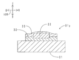
- FIG. 2 is an exploded cross-sectional view in the II-II direction of FIG. 1. It is an enlarged view in the frame III of FIG.
- FIG. 4 is a cross-sectional view in the IV-IV direction of FIG. 3.
- FIG. 5 is a cross-sectional view in the VV direction of FIG. 3.
- Capacitance type sensor transducer
- 11 dielectric layer
- 12 fusion part
- 20 front side sheet member
- 21 front side base material
- 30 back side sheet member
- 31 back side base material
- 32 second Conductive layer
- 33 first conductive layer
- 34 protective layer
- 35 reinforcing layer
- 320 recess
- 330 terminal portion.
- 01X to 08X Front side electrode
- 01Y to 08Y Back side electrode
- 01x to 08x Front side wiring part
- 200x Connection end part
- 01y to 08y Back side wiring part
- 300y Connection end part
- the flexible conductive member and the transducer of the present invention are not limited to the following forms, and can be variously modified and improved by those skilled in the art without departing from the gist of the present invention. Can be implemented.
- the flexible conductive member of the present invention includes a base material having stretchability, and a plurality of conductive layers arranged in at least one of a laminated and parallel form on the surface of the base material.
- the substrate is not particularly limited as long as it can expand and contract and can form a conductive layer.
- the substrate include resin films such as polyimide, polyethylene, polyethylene terephthalate (PET), and polyethylene naphthalate (PEN), elastomer sheets, and stretchable fabrics.
- the conductive layer at least a first conductive layer and a second conductive layer described later are disposed. In addition to the first conductive layer and the second conductive layer, another type of conductive layer may be disposed.
- the conductive layers are arranged in the form of lamination, parallel, or a combination thereof. When arranged in parallel, the conductive layers may or may not be in contact with each other. When the conductive layers are not in contact with each other, the individual conductive layers are electrically connected in parallel.
- the flexible conductive member of the present invention may include a protective layer for covering the conductive layer in addition to the conductive layer.
- the first conductive layer which is one of the conductive layers, is made of a highly conductive material containing an elastomer and a conductive material and having a volume resistivity of 5 ⁇ 10 ⁇ 2 ⁇ ⁇ cm or less when not stretched. From the viewpoint of making the conductivity higher, the volume resistivity of the highly conductive material when not stretched is preferably 1 ⁇ 10 ⁇ 3 ⁇ ⁇ cm or less.
- the elastomer is not particularly limited.
- urethane rubber acrylic rubber, silicone rubber, ethylene-propylene copolymer rubber, natural rubber, styrene-butadiene copolymer rubber, acrylonitrile-butadiene copolymer rubber, epichlorohydrin rubber, chlorosulfonated polyethylene, chlorinated polyethylene, etc. Is preferred.
- a conductive material silver, gold, copper, nickel, rhodium, palladium, chromium, titanium, platinum, iron, and alloys thereof are used so that the volume resistivity when not stretched is 5 ⁇ 10 ⁇ 2 ⁇ ⁇ cm or less.
- a metal powder such as One kind of metal powder can be used alone, or two or more kinds can be mixed and used. Of these, silver powder is preferred. What is necessary is just to determine the compounding quantity of metal powder suitably so that it may become a desired volume resistivity. For example, it is desirably 200 parts by mass or more with respect to 100 parts by mass of the elastomer. On the other hand, when the amount of the metal powder is increased, the flexibility is lowered. Therefore, the blending amount of the metal powder is desirably 500 parts by mass or less with respect to 100 parts by mass of the elastomer.
- the second conductive layer which is another one of the conductive layers, has a volume resistivity at the time of non-stretching that is larger than the volume resistivity at the time of non-stretching of the highly conductive material, and includes an elastomer and a conductive material. It consists of a highly extensible conductive material whose volume resistivity change at 50% elongation is 10 times or less.
- the elastomer may be the same as or different from the elastomer of the first conductive layer. What is necessary is just to select suitably from the elastomer enumerated in description of the said 1st conductive layer.
- the conductive material it is desirable to use conductive carbon powder such as carbon black, carbon nanotube, and graphite.
- the volume resistivity of the highly stretchable conductive material when not stretched is larger than the volume resistivity of the high conductivity material when not stretched.
- the volume resistivity of the highly extensible conductive material when not stretched is desirably 1 ⁇ 10 1 ⁇ ⁇ cm or less.
- the difference between the volume resistivity of the highly conductive material when not stretched and the volume resistivity of the highly stretchable conductive material when not stretched is desirably 5 digits or less.
- the type and blending amount of the conductive carbon powder may be appropriately adjusted.
- the blending amount of the conductive carbon powder is desirably 10 parts by mass or more with respect to 100 parts by mass of the elastomer.
- the compounding amount of the conductive carbon powder is desirably 100 parts by mass or less with respect to 100 parts by mass of the elastomer.
- the highly extensible conductive material is smaller than the highly conductive material.
- the volume resistivity of the highly extensible conductive material is unlikely to increase even when elongated.
- the change in volume resistivity at the time of 50% elongation with respect to the unextended state is 10 times or less.
- the elastic modulus of the highly extensible conductive material is desirably 50 MPa or less.
- the conductive layers are arranged in the form of lamination, parallel, or a combination thereof.
- the first conductive layer and the second conductive layer are desirably laminated from the viewpoint of improving durability against expansion and contraction due to the reinforcing effect between the conductive layers.
- the first conductive layer contains metal powder and the second conductive layer contains conductive carbon powder
- the first conductive layer can be reinforced.
- the adhesion between the two layers is increased. That is, if the surface roughness of the laminated surface of the conductive layer is large, the conductive layer is difficult to peel off due to the anchor effect even if the expansion and contraction are repeated. Further, when the adhesion between the conductive layers to be stacked is large, the stress at the time of expansion / contraction is transmitted not only to one conductive layer but also to the entire conductive layer, so that the durability of the entire conductive layer is improved.
- the surface roughness of the conductive layer disposed on the substrate side may be 1/200 or more of the thickness of the conductive layer.
- the surface roughness of the conductive layer disposed on the substrate side may be set to be twice or less the thickness of the conductive layer.
- the surface roughness of the second conductive layer tends to be larger.
- the value calculated by the following method is adopted as the surface roughness of the conductive layer.
- the cross section of the conductive layer in the stacking direction is observed with a scanning electron microscope (SEM), and the reference line of the interface of the conductive layer to be measured is determined.
- the sum total of the areas of the peaks protruding from the reference line (S1) and the sum of the areas of the recessed valleys (S2) are calculated.
- surface roughness is calculated by following Formula (1).
- Surface roughness (S1 + S2) / length of reference line (1)
- the method for forming the conductive layer is not particularly limited.
- a pre-formed conductive layer may be attached to the substrate, or a conductive paint may be printed.
- the printing method it is possible to easily form a long, thin line, or thin film conductive layer.
- the printing method include inkjet printing, flexographic printing, gravure printing, screen printing, pad printing, and lithography.
- the screen printing method is preferred because the coating thickness can be easily adjusted and the dimensional accuracy is high.
- the conductive layer is formed by a printing method
- the compatibility between the solvent contained in the conductive paint and the polymer contained in the member it is preferable to consider the compatibility between the solvent contained in the conductive paint and the polymer contained in the member to be printed.
- the polymer of the base material and the solvent contained in the conductive paint are highly compatible (both SP values (solubility parameters) of both are close)
- the solvent will be used when the conductive paint is printed on the base material.
- the base material will swell due to penetration.
- the compatibility between the first-layer elastomer and the solvent contained in the conductive paint forming the second layer is better. If the compatibility between the two is low, the conductive paint is not well adapted to the first layer, and the second layer may not be formed uniformly.
- the transducer of the present invention includes the flexible conductive member of the present invention.
- An embodiment of a capacitive sensor will be described as an example of the transducer of the present invention.
- the flexible conductive member of the present invention is embodied as a wiring structure.
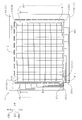
- FIG. 1 shows a top transparent view of the capacitive sensor of this embodiment.
- FIG. 2 shows an exploded sectional view in the II-II direction of FIG.
- FIG. 3 shows an enlarged view in the frame III of FIG.
- FIG. 4 shows a cross-sectional view in the IV-IV direction of FIG.
- FIG. 5 shows a cross-sectional view in the VV direction of FIG.
- stacked on the front and back direction (thickness direction) is permeate
- the capacitive sensor 1 of this embodiment includes a dielectric layer 11, a front side sheet member 20, and a back side sheet member 30.
- the dielectric layer 11 is made of urethane foam and has a rectangular sheet shape.
- the thickness of the dielectric layer 11 is 300 ⁇ m.
- the dielectric layer 11 extends in the XY directions (left and right and front and rear directions).
- the front sheet member 20 and the back sheet member 30 are laminated with the dielectric layer 11 interposed therebetween.
- the back sheet member 30 is disposed on the lower side (back side) of the dielectric layer 11.
- the back side sheet member 30 includes a back side base material 31, back side electrodes 01Y to 08Y, and back side wiring portions 01y to 08y.
- the back side base material 31 is made of polyethylene terephthalate (PET) and has a rectangular shape.
- a total of eight back side electrodes 01Y to 08Y are formed on the upper surface (surface) of the back side base material 31.
- Each of the back side electrodes 01Y to 08Y has a strip shape.
- the back-side electrodes 01Y to 08Y each extend in the X direction (left-right direction).
- the back-side electrodes 01Y to 08Y are arranged in the Y direction (front-rear direction) so as to be substantially parallel to each other at a predetermined interval.
- the back-side electrodes 01Y to 08Y each contain acrylic rubber, carbon black, and carbon nanotube.
- a terminal portion 330 is disposed on the upper surface of the left end portion of each of the back-side electrodes 01Y to 08Y.
- the terminal portions 330 each have a rectangular shape.
- a portion of the terminal portion 330 extends to the left and is connected to a first conductive layer 33 of backside wiring portions 01y to 08y described later.
- the terminal portion 330 is made of the same highly conductive material as the first conductive layer 33, and contains urethane rubber and silver powder.
- a total of eight back side wiring portions 01y to 08y are formed on the upper surface of the back side base material 31.
- Each of the back side wiring portions 01y to 08y has a linear shape.
- the back side wiring portions 01y to 08y are connected to the left end portions of the back side electrodes 01Y to 08Y, respectively.
- the laminated portions of the back side base material 31 and the back side wiring portions 01y to 08y in the back side sheet member 30 are each included in the flexible conductive member of the present invention.
- 3 is partially enlarged, and as shown in FIG. 4 which is a cross-sectional view of the back-side wiring portion 01y, the back-side wiring portions 01y to 08y each have the first conductive layer 33 except for the connection end portion 300y. And a second conductive layer 32 and a protective layer 34.
- the second conductive layer 32 is disposed on the upper surface of the back side base material 31.
- the second conductive layer 32 is made of the same highly extensible conductive material as the back side electrodes 01Y to 08Y, and includes acrylic rubber, carbon black, and carbon nanotubes.
- the second conductive layer 32 is formed continuously with each of the back-side electrodes 01Y to 08Y.
- the volume resistivity of the highly stretchable conductive material (second conductive layer 32) when not stretched is 2.0 ⁇ 10 ⁇ 1 ⁇ ⁇ cm, and the volume resistivity when stretched 50% is 7.0 ⁇ 10 ⁇ 1 ⁇ ⁇ cm. cm and the elastic modulus is 20 MPa.
- the surface roughness of the upper surface of the second conductive layer 32 is 1.98 ⁇ m.
- the second conductive layer 32 has a width of 4 mm and a thickness of 10 ⁇ m.
- a recess 320 extending in the longitudinal direction is formed on the upper surface of the second conductive layer 32.
- the first conductive layer 33 is stacked on the upper surface of the second conductive layer 32.
- the lower part of the first conductive layer 33 is disposed in the recess 320 of the second conductive layer 32.
- the first conductive layer 33 is made of a highly conductive material and includes urethane rubber and silver powder.
- the volume resistivity of the highly conductive material (first conductive layer 33) when not stretched is 6.7 ⁇ 10 ⁇ 5 ⁇ ⁇ cm, and the volume resistivity when stretched 50% is 2.0 ⁇ 10 ⁇ 3 ⁇ ⁇ cm.
- the elastic modulus is 100 MPa.
- the first conductive layer 33 has a width of 1 mm and a thickness of 50 ⁇ m.
- the first conductive layer 33 is formed continuously with each of the terminal portions 330 of the back-side electrodes 01Y to 08Y.
- the protective layer 34 is disposed on the upper surface of the back substrate 31 so as to cover the second conductive layer 32 and the first conductive layer 33.
- the protective layer 34 is made of silicone rubber.
- connection end portion 300y that is electrically connected to a measurement circuit (not shown) is disposed at the front end portion of each of the back side wiring portions 01y to 08y.
- each of the connection end portions 300y includes a first conductive layer 33, a second conductive layer 32, and a reinforcing layer 35.
- the reinforcing layer 35 is laminated on the upper surface of the second conductive layer 32 so as to cover the first conductive layer 33.
- the first conductive layer 33 is sandwiched between the second conductive layer 32 and the reinforcing layer 35.
- the reinforcing layer 35 includes a polyester resin and carbon black.
- the front sheet member 20 is disposed on the upper side (front side) of the dielectric layer 11.
- the front sheet member 20 includes a front substrate 21, front electrodes 01X to 08X, and front wiring portions 01x to 08x.
- the front-side base material 21 is made of PET and has the same rectangular shape as the back-side base material 31.
- a total of eight front side electrodes 01X to 08X are formed on the lower surface (back surface) of the front side base material 21.
- the front electrodes 01X to 08X each have a strip shape.
- the front-side electrodes 01X to 08X each extend in the Y direction (front-rear direction).
- the front-side electrodes 01X to 08X are arranged in the X direction (left-right direction) so as to be substantially parallel to each other with a predetermined interval.
- the front-side electrodes 01X to 08X each contain acrylic rubber, carbon black, and carbon nanotube. Terminal portions are arranged on the lower surfaces of the front end portions of the front side electrodes 01X to 08X, similarly to the back side electrodes 01Y to 08Y.
- a part of the terminal portion extends forward and is connected to second conductive layers of front side wiring portions 01x to 08x described later.
- the terminal portion is made of the same highly conductive material as the front side wiring portions 01x to 08x, and includes urethane rubber and silver powder.
- a total of eight front side wiring portions 01x to 08x are formed on the lower surface of the front side base material 21.
- the front side wiring portions 01x to 08x each have a linear shape.
- the front side wiring portions 01x to 08x are connected to the front end portions of the front side electrodes 01X to 08X, respectively.
- Each of the laminated portions of the front side base member 21 and the front side wiring portions 01x to 08x in the front side sheet member 20 is included in the flexible conductive member of the present invention.
- the configuration of the front side wiring portions 01x to 08x is the same as the configuration of the back side wiring portions 01y to 08y. Therefore, a brief description will be given below.
- the front wiring parts 01x to 08x each have a first conductive layer, a second conductive layer, and a protective layer, except for the connection end part 200x.
- the second conductive layer is disposed on the lower surface of the front side base material 21.
- the second conductive layer is made of the same highly extensible conductive material as the front electrodes 01X to 08X, and is formed continuously with each of the front electrodes 01X to 08X.
- a recess extending in the longitudinal direction is formed on the lower surface of the second conductive layer.
- the first conductive layer is laminated on the lower surface of the second conductive layer.
- the upper part of the first conductive layer is disposed in the recess of the second conductive layer.
- the width of the first conductive layer is smaller than the width of the second conductive layer.
- the first conductive layer is made of a highly conductive material, and is formed continuously with each of the terminal portions of the front side electrodes 01X to 08X.
- the protective layer is disposed on the lower surface of the front-side base material 21 so as to cover the first conductive layer and the second conductive layer.
- connection end portion 200x that is electrically connected to a measurement circuit (not shown) is disposed at the left end portion of each of the front side wiring portions 01x to 08x.
- Each of the connection end portions 200x includes a first conductive layer, a second conductive layer, and a reinforcing layer.
- the reinforcing layer is laminated on the lower surface of the second conductive layer so as to cover the first conductive layer.
- the first conductive layer is sandwiched between the second conductive layer and the reinforcing layer.
- a plurality of fused portions 12 are arranged on the peripheral edge portions of the front side sheet member 20 and the back side sheet member 30.
- the plurality of fused portions 12 are arranged in a dotted line so as to surround the periphery of the dielectric layer 11.
- the front side sheet member 20 and the back side sheet member 30 are joined at the fusion part 12.
- the detection units A0101 to A0808 are arranged at portions (overlapping portions) where the front side electrodes 01X to 08X and the back side electrodes 01Y to 08Y intersect when viewed in the vertical direction.
- Each of the detection units A0101 to A0808 includes a part of the front side electrodes 01X to 08X, a part of the back side electrodes 01Y to 08Y, and a part of the dielectric layer 11.
- the detectors A0101 to A0808 are arranged at substantially equal intervals over substantially the entire surface of the dielectric layer 11.
- a load distribution is detected in a rectangular region surrounding the detection units A0101 to A0808.
- the sign “AOO ⁇ ” of the detection unit the upper two digits “OO” correspond to the front electrodes 01X to 08X.
- the last two digits “ ⁇ ” correspond to the backside electrodes 01Y to 08Y.
- the manufacturing method of the capacitive sensor 1 of the present embodiment includes a sheet member manufacturing process, a stacking process, and a fusing process.
- the following four types of paints are prepared.
- Reinforcing layer coating material for forming the reinforcing layer 35.
- the prepared four kinds of paints are appropriately screen-printed on the lower surface of the front substrate 21 (the lower surface in FIG. 1 and arranged upward at the time of printing) and cured by heating, whereby the front electrodes 01X to 08X. And the front side wiring parts 01x to 08x are formed.
- the front sheet member 20 is produced.
- the four types of prepared paints are appropriately screen-printed on the upper surface of the back-side base material 31 and heat-cured to form the back-side electrodes 01Y to 08Y and the back-side wiring portions 01y to 08y.
- the back side sheet member 30 is produced.
- the back sheet member 30, the dielectric layer 11, and the front sheet member 20 are stacked in order from the bottom. That is, the back side sheet is arranged such that the dielectric layer 11 is interposed between the back side electrodes 01Y to 08Y formed on the top surface of the back side base material 31 and the front side electrodes 01X to 08X formed on the bottom surface of the front side base material 21.
- the member 30, the dielectric layer 11, and the front sheet member 20 are laminated.
- the peripheral portions of the laminated front side sheet member 20 and back side sheet member 30 are spot fused at a predetermined interval (see the fused part 12 in FIG. 1). In this way, the capacitive sensor 1 of the present embodiment is manufactured.
- the distance between the front side electrode and the back side electrode becomes small. Thereby, the electrostatic capacitance C of the said detection part becomes large.
- the load for each of the detection units A0101 to A0808 is calculated from the change amount ⁇ C of the capacitance C.
- the wiring part of the capacitive sensor 1 of the present embodiment is made of the flexible conductive member of the present invention. That is, the back side wiring portions 01y to 08y formed on the upper surface of the back side base material 31 have the first conductive layer 33 and the second conductive layer 32, respectively. Similarly, the front-side wiring portions 01x to 08x formed on the lower surface of the front-side base material 21 each have a first conductive layer and a second conductive layer.
- the first conductive layer 33 is made of a highly conductive material
- the second conductive layer 32 is made of a highly extensible conductive material.
- the electrical resistance is small because the electrical conduction is mainly performed through the first conductive layer 33. Further, since electrical conduction is mainly performed through the second conductive layer 32 during expansion, the electrical resistance is small.
- an advantageous conduction path is selected according to the state, so that the desired conductivity is maintained both in the natural state and at the time of extension. be able to. Therefore, even if the expansion and contraction is repeated, the electric resistance is unlikely to increase.
- the front side wiring portions 01x to 08x and the back side wiring portions 01y to 08y are excellent in durability against expansion and contraction.
- the surface roughness of the upper surface (surface on which the first conductive layer 33 is laminated) of the second conductive layer 32 disposed on the back side base material 31 side is 1.98 ⁇ m. The value of the surface roughness is about 1/5 of the thickness of the second conductive layer 32. For this reason, the adhesive force between the first conductive layer 33 and the second conductive layer 32 is large.
- the base material / second conductive layer / first conductive layer are stacked in this order.
- the base material / first conductive layer / second conductive layer is stacked in this order. May be.
- the front side wiring parts 01x to 08x and the back side wiring parts 01y to 08y have a protective layer 34 made of silicone rubber except for the connection end parts 200x and 300y. For this reason, the silver powder contained in the first conductive layer 33 is not easily oxidized. Therefore, even if it uses for a long period of time, the electroconductivity of the 1st conductive layer 33 does not fall easily. Further, by covering with the protective layer 34, insulation from the outside can be ensured. Further, the reinforcing effect of the front side wiring parts 01x to 08x and the back side wiring parts 01y to 08y can be expected.
- connection end portions 200x and 300y the front-side wiring portions 01x to 08x and the back-side wiring portions 01y to 08y have a reinforcing layer 35 containing carbon black.
- the strength of the connection end portions 200x and 300y is increased, and the durability is improved.
- the capacitive sensor 1 is excellent in durability.
- First conductive paint A was prepared as follows. First, 100 parts by mass of a urethane rubber polymer (“Byron (registered trademark) BX1001” manufactured by Toyobo Co., Ltd.) was dissolved in butyl carbitol acetate as a solvent. To this urethane rubber solution, 400 parts by mass of silver powder (“Ag-XF301” manufactured by Fukuda Metal Foil Industry Co., Ltd.) was added and stirred.
- a urethane rubber polymer (“Byron (registered trademark) BX1001” manufactured by Toyobo Co., Ltd.) was dissolved in butyl carbitol acetate as a solvent.
- silver powder Ag-XF301 manufactured by Fukuda Metal Foil Industry Co., Ltd.
- a second conductive paint B was prepared as follows. First, 100 parts by mass of an acrylic rubber polymer (“NIPOL (registered trademark) AR42W” manufactured by Nippon Zeon Co., Ltd.) and 0.1 part by mass of ethylenediamine as a cross-linking agent are mixed in a roll kneader, and an acrylic rubber composition is prepared. Was prepared. Subsequently, the prepared acrylic rubber composition was dissolved in butyl carbitol acetate to prepare an acrylic rubber solution.
- NIPOL registered trademark
- AR42W manufactured by Nippon Zeon Co., Ltd.
- Second conductive paints C and D were prepared in the same manner as the second conductive paint B, except that the blending amounts of carbon nanotubes and carbon black were changed.
- Each of the prepared conductive paints was subjected to bar coat printing on a base material (release PET film) to produce conductive layers A to D.
- the first conductive layer A is made of a highly conductive material.
- the second conductive layers B to D are made of a highly extensible conductive material.
- the elastic modulus of each conductive layer, elongation at the time of cutting, volume resistivity at the time of non-extension, volume resistivity at the time of 50% extension, and surface roughness were measured.
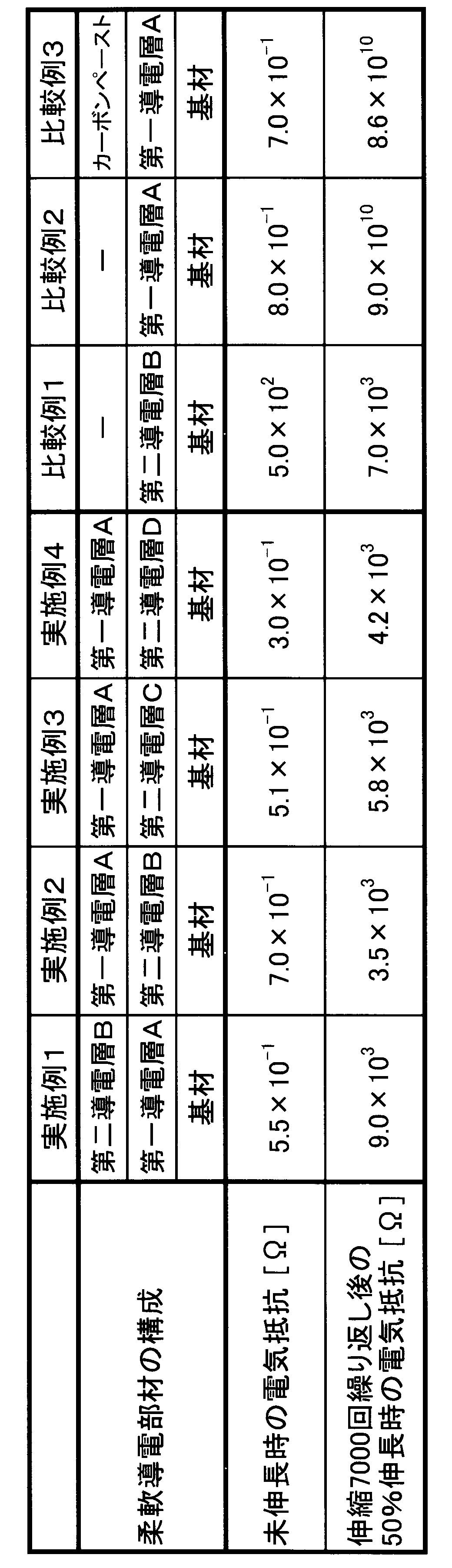
- the measuring method is as follows. Table 1 below shows the measurement results of the composition and physical properties of each conductive layer. In Table 1, the unit of the blending amount of raw materials is parts by mass.
- volume resistivity The volume resistivity was measured according to the parallel terminal electrode method of JIS K6271 (2008). The distance between the electrodes when not stretched was 10 mm. A commercially available silicone rubber sheet (manufactured by Kureha Elastomer Co., Ltd.) was used as an insulating resin support for supporting the test piece.
- a flexible conductive member composed of a base material / first conductive layer A / second conductive layer B was produced as follows. First, the first conductive paint A was screen-printed on the upper surface of the substrate. And the formed coating film of the first conductive paint A was pre-dried to a semi-cured state. Next, the second conductive paint B was screen-printed on the upper surface of the semiconductive film of the first conductive paint A. Finally, the formed coating film was cured by heating to form two conductive layers A and B.
- Example 2 The flexible conductive member consisting of the base material / second conductive layer B / first conductive layer A was manufactured by changing the printing order of the conductive paint.
- the method for forming the conductive layer is the same as that in Example 1.
- Example 3 The 2nd conductive paint B in Example 2 was changed into the 2nd conductive paint C, and the flexible conductive member which consists of a base material / 2nd conductive layer C / 1st conductive layer A was manufactured.
- Example 4 The 2nd conductive paint B in Example 2 was changed into the 2nd conductive paint D, and the flexible conductive member which consists of a base material / 2nd conductive layer D / 1st conductive layer A was manufactured.
- a second conductive paint B was screen-printed on the upper surface of the base material, and the coating film was cured by heating to produce a flexible conductive member composed of the base material / second conductive layer B.
- a first conductive paint A was screen-printed on the upper surface of the substrate, and the coating film was cured by heating to produce a flexible conductive member composed of the substrate / second conductive layer A.
- the first conductive paint A was screen printed on the upper surface of the substrate. And the formed coating film of the first conductive paint A was pre-dried to a semi-cured state. Next, a carbon paste (“JELCON CH-8” manufactured by Jujo Chemical Co., Ltd.) was screen-printed on the upper surface of the semiconductive film of the first conductive paint A. Finally, the formed coating film was cured by heating to form two conductive layers.
- the volume resistivity of the conductive layer formed from the carbon paste when not stretched is 1.0 ⁇ 10 ⁇ 2 ⁇ ⁇ cm. Moreover, the elastic modulus of the conductive layer was 1200 MPa, and it broke when it was stretched 50%. Therefore, the upper conductive layer is not included in the second conductive layer of the present invention.
- Terminals were arranged at both ends in the length direction of the upper conductive layer, and the electrical resistance when not stretched and the electrical resistance when stretched 50% after the stretch durability test were measured.
- the stretch durability test was performed as follows. First, both ends of the flexible conductive member were sandwiched between a pair of jigs. Next, the flexible conductive member was expanded and contracted by fixing one of the jigs and reciprocating the other at a speed of 50 mm / min. The elongation rate of the flexible conductive member was 50%, and the number of expansions / contractions was 7000 times. Table 2 shows the measurement results.
- the flexible conductive member of the present invention including the first conductive layer and the second conductive layer has high conductivity in the natural state and small decrease in conductivity even after repeated expansion and contraction.
- butyl carbitol acetate was used as a solvent for the first conductive paint and the second conductive paint.
- the compatibility between butyl carbitol acetate and acrylic rubber is high, but the compatibility between butyl carbitol acetate and urethane rubber is not so high.
- the base material / second conductive layer (acrylic rubber) / first conductive are suitable.
- the flexible conductive member of the present invention is suitable for flexible transducer electrodes and wiring using elastomer. Further, it is also suitable as a wiring of a flexible wiring board used for a bendable display or the like, a control device for a movable part of a robot or an industrial machine, an electrode of a wearable device, or a wiring. Furthermore, it can be used as a conductive adhesive or an electromagnetic wave shield. Also, in motors and actuators that are driven electromagnetically, speakers using a piezoelectric effect, vibrators, ultrasonic generators, etc., disconnection due to repeated vibrations becomes a problem.
- the flexible conductive member of the present invention can be applied to a portion requiring durability against repeated vibration in a wide frequency range regardless of the magnitude of displacement.
Landscapes
- Engineering & Computer Science (AREA)
- Microelectronics & Electronic Packaging (AREA)
- Physics & Mathematics (AREA)
- General Physics & Mathematics (AREA)
- Signal Processing (AREA)
- Power Engineering (AREA)
- Acoustics & Sound (AREA)
- Chemical & Material Sciences (AREA)
- Dispersion Chemistry (AREA)
- Laminated Bodies (AREA)
- Parts Printed On Printed Circuit Boards (AREA)
- Force Measurement Appropriate To Specific Purposes (AREA)
- Electrostatic, Electromagnetic, Magneto- Strictive, And Variable-Resistance Transducers (AREA)
- Non-Insulated Conductors (AREA)
Abstract
Description
01X~08X:表側電極、01Y~08Y:裏側電極、01x~08x:表側配線部、200x:接続端部、01y~08y:裏側配線部、300y:接続端部、A0101~A0808:検出部。
本発明の柔軟導電部材は、伸縮性を有する基材と、該基材の表面に積層および並列の少なくとも一方の形態で配置される複数の導電層と、を備える。
表面粗さ=(S1+S2)/基準線の長さ・・・(1)
本発明の柔軟導電部材において、導電層の形成方法は、特に限定されない。予め形成された導電層を基材に貼着してもよく、導電塗料を印刷してもよい。印刷法によると、長尺、細線、薄膜状の導電層を、容易に形成することができる。印刷法としては、例えば、インクジェット印刷、フレキソ印刷、グラビア印刷、スクリーン印刷、パッド印刷、リソグラフィー等が挙げられる。なかでも、塗膜厚さの調整が容易であり、寸法精度も高いという理由から、スクリーン印刷法が好適である。
本発明のトランスデューサは、上記本発明の柔軟導電部材を備える。本発明のトランスデューサの一例として、静電容量型センサの実施形態を説明する。本実施形態の静電容量型センサにおいて、本発明の柔軟導電部材は、配線構造として具現化されている。
まず、本実施形態の静電容量型センサの構成について説明する。図1に、本実施形態の静電容量型センサの上面透過図を示す。図2に、図1のII-II方向分解断面図を示す。図3に、図1の枠III内の拡大図を示す。図4に、図3のIV-IV方向断面図を示す。図5に、図3のV-V方向断面図を示す。図1においては、表裏方向(厚さ方向)に積層される部材を透過して示す。図1、図3においては、保護層を省略して示す。
次に、本実施形態の静電容量型センサ1の製造方法について説明する。本実施形態の静電容量型センサ1の製造方法は、シート部材作製工程と、積層工程と、融着工程と、を有している。
(1)表側電極01X~08X、裏側電極01Y~08Y、表側配線部01x~08xおよび裏側配線部01y~08yの第二導電層、を形成するための第二導電塗料。
(2)表側配線部01x~08xおよび裏側配線部01y~08yの第一導電層を形成するための第一導電塗料。
(3)保護層34を形成するための保護層用塗料。
(4)補強層35を形成するための補強層用塗料。
次に、本実施形態の静電容量型センサ1の動きについて説明する。まず、静電容量型センサ1に荷重が加わる前(初期状態)に、表側電極01X~08X、裏側電極01Y~08Yに電圧を印加して、検出部A0101~A0808ごとに、静電容量Cを算出する。すなわち、検出部A0101から検出部A0808までを、あたかも走査するように、静電容量Cを算出する。続いて、静電容量型センサ1に荷重が加わった後も同様に、検出部A0101~A0808ごとに、静電容量Cを算出する。荷重が加わった部分の検出部においては、表側電極と裏側電極との距離が小さくなる。これにより、当該検出部の静電容量Cは、大きくなる。この静電容量Cの変化量ΔCから、検出部A0101~A0808ごとの荷重が算出される。
次に、本実施形態の静電容量型センサ1の作用効果について説明する。本実施形態の静電容量型センサ1の配線部は、本発明の柔軟導電部材からなる。すなわち、裏側基材31の上面に形成された裏側配線部01y~08yは、各々、第一導電層33と第二導電層32とを有する。同様に、表側基材21の下面に形成された表側配線部01x~08xは、各々、第一導電層と第二導電層とを有する。第一導電層33は高導電性材料からなり、第二導電層32は高伸長性導電材料からなる。自然状態(未伸長)においては、主に第一導電層33を介して導通するため、電気抵抗は小さい。また、伸長時においては、主に第二導電層32を介して導通するため、電気抵抗は小さい。このように、表側配線部01x~08x、裏側配線部01y~08yにおいては、状態に応じて有利な導通経路が選択されるため、自然状態においても伸長時においても、所望の導電性を維持することができる。よって、伸縮を繰り返しても電気抵抗が増加しにくい。
次のようにして第一導電塗料Aを調製した。まず、ウレタンゴムポリマー(東洋紡(株)製「バイロン(登録商標)BX1001」)100質量部を、溶剤のブチルカルビトールアセテートに溶解させた。このウレタンゴム溶液に、銀粉末(福田金属箔粉工業(株)製「Ag-XF301」)400質量部を添加して、攪拌した。
次のようにして第二導電塗料Bを調製した。まず、アクリルゴムポリマー(日本ゼオン(株)製「ニポール(登録商標)AR42W」)100質量部と、架橋剤のエチレンジアミン0.1質量部と、をロール練り機にて混合し、アクリルゴム組成物を調製した。続いて、調製したアクリルゴム組成物を、ブチルカルビトールアセテートに溶解させて、アクリルゴム溶液を調製した。このアクリルゴム溶液に、カーボンナノチューブ(昭和電工(株)製「VGCF(登録商標)」)20質量部、およびカーボンブラック(ケッチェンブラックインターナショナル(株)製「ケッチェンブラックEC300JD」)17質量部を添加して、撹拌した。また、カーボンナノチューブおよびカーボンブラックの配合量を変更した以外は、第二導電塗料Bと同様にして、第二導電塗料C、Dを調製した。
調製した各導電塗料を基材(離型PETフィルム)にバーコート印刷して、A~Dの導電層を製造した。第一導電層Aは、高導電性材料からなる。第二導電層B~Dは、高伸長性導電材料からなる。そして、各導電層の弾性率、切断時伸び、未伸長時の体積抵抗率、50%伸長時の体積抵抗率、および表面粗さを測定した。測定方法は次の通りである。各導電層の組成、および物性等の測定結果を、下記表1に示す。表1中、原料の配合量の単位は質量部である。
JIS K7127(1999)に準じた引張試験を行って、得られた応力-伸び曲線から弾性率を算出した。試験片にはタイプ2を使用した。
JIS K6251(2010)に準じた引張試験を行って、切断時伸び(Eb)を算出した。試験片にはダンベル状5号形を使用し、伸長速度は100mm/minとした。
JIS K6271(2008)の平行端子電極法に準じて、体積抵抗率を測定した。未伸長時の電極間距離は、10mmとした。試験片を支持する絶縁樹脂製支持具には、市販のシリコーンゴムシート(クレハエラストマー(株)製)を用いた。
導電層の断面のSEM写真から、上述した式(1)により、表面粗さを算出した。

調製した第一導電塗料Aと、第二導電塗料B~Dのいずれかと、を使用して、基材の表面に導電層を二層形成し、柔軟導電部材を製造した。基材には、ウレタンエラストマーシートを使用した。第一導電塗料Aから形成される第一導電層の大きさは、幅2mm、長さ20mm、厚さ25μmとした。第二導電塗料B~Dのいずれかから形成される第二導電層の大きさは、幅10mm、長さ20mm、厚さ10μmとした。実施例1~4の柔軟導電部材は、本発明の柔軟導電部材に含まれる。
次のようにして、基材/第一導電層A/第二導電層Bからなる柔軟導電部材を製造した。まず、基材の上面に、第一導電塗料Aをスクリーン印刷した。そして、形成された第一導電塗料Aの塗膜を予備乾燥して、半硬化状態にした。次に、半硬化状態の第一導電塗料Aの塗膜の上面に、第二導電塗料Bをスクリーン印刷した。最後に、形成した塗膜を、加熱により硬化して、A、B二層の導電層を形成した。
導電塗料の印刷順を変更して、基材/第二導電層B/第一導電層Aからなる柔軟導電部材を製造した。導電層の形成方法は実施例1と同じである。
実施例2における第二導電塗料Bを第二導電塗料Cに変更して、基材/第二導電層C/第一導電層Aからなる柔軟導電部材を製造した。
実施例2における第二導電塗料Bを第二導電塗料Dに変更して、基材/第二導電層D/第一導電層Aからなる柔軟導電部材を製造した。
基材の上面に、第二導電塗料Bをスクリーン印刷し、加熱により塗膜を硬化して、基材/第二導電層Bからなる柔軟導電部材を製造した。
基材の上面に、第一導電塗料Aをスクリーン印刷し、加熱により塗膜を硬化して、基材/第二導電層Aからなる柔軟導電部材を製造した。
基材の上面に、第一導電塗料Aをスクリーン印刷した。そして、形成された第一導電塗料Aの塗膜を予備乾燥して、半硬化状態にした。次に、半硬化状態の第一導電塗料Aの塗膜の上面に、カーボンペースト(十条ケミカル(株)製「JELCON CH-8」)をスクリーン印刷した。最後に、形成した塗膜を、加熱により硬化して、二層の導電層を形成した。カーボンペーストから形成された導電層の未伸長時の体積抵抗率は、1.0×10⁻²Ω・cmである。また、当該導電層の弾性率は1200MPaであり、50%伸長させると破断した。したがって、上層の導電層は、本発明の第二導電層には含まれない。
上側の導電層の長さ方向両端部に端子を配置して、未伸長時の電気抵抗と、伸縮耐久試験後の50%伸長時の電気抵抗と、を測定した。伸縮耐久試験は、次のようにして行った。まず、柔軟導電部材の両端部を、一対のジグで挟持した。次に、ジグの一方を固定し、他方を50mm/分の速度で往復動させることにより、柔軟導電部材を伸縮させた。柔軟導電部材の伸長率は50%とし、伸縮回数は7000回とした。表2に、測定結果を示す。
Claims (9)
- 伸縮性を有する基材と、
該基材の表面に積層および並列の少なくとも一方の形態で配置される複数の導電層と、
を備え、
該導電層は、エラストマーおよび導電材を含み未伸長時の体積抵抗率が5×10⁻²Ω・cm以下の高導電性材料からなる第一導電層と、未伸長時の体積抵抗率が該高導電性材料の未伸長時の体積抵抗率よりも大きく、エラストマーおよび導電材を含み未伸長時に対する50%伸長時の体積抵抗率の変化が10倍以下の高伸長性導電材料からなる第二導電層と、を有することを特徴とする柔軟導電部材。 - 前記高導電性材料の未伸長時の体積抵抗率と、前記高伸長性導電材料の未伸長時の体積抵抗率と、の差は5桁以下である請求項1に記載の柔軟導電部材。
- 前記高伸長性導電材料の弾性率は、50MPa以下である請求項1または請求項2に記載の柔軟導電部材。
- 前記高伸長性導電材料に含まれる前記導電材は、導電性炭素粉末である請求項1ないし請求項3のいずれかに記載の柔軟導電部材。
- 前記高導電性材料に含まれる前記導電材は、金属粉末である請求項1ないし請求項4のいずれかに記載の柔軟導電部材。
- 前記第一導電層および前記第二導電層は積層される請求項1ないし請求項5のいずれかに記載の柔軟導電部材。
- 前記第一導電層および前記第二導電層のうち、前記基材側に配置される導電層の表面粗さは、該導電層の厚さの1/200以上2倍以下である請求項6に記載の柔軟導電部材。
- 前記基材の表面に前記第二導電層が配置され、該第二導電層の表面に前記第一導電層が配置される請求項6または請求項7に記載の柔軟導電部材。
- 請求項1ないし請求項8のいずれかに記載の柔軟導電部材を備えることを特徴とするトランスデューサ。
Priority Applications (5)
| Application Number | Priority Date | Filing Date | Title |
|---|---|---|---|
| PCT/JP2012/080158 WO2014080470A1 (ja) | 2012-11-21 | 2012-11-21 | 柔軟導電部材およびそれを用いたトランスデューサ |
| EP12888811.2A EP2924695A4 (en) | 2012-11-21 | 2012-11-21 | FLEXIBLE CONDUCTIVE ELEMENT AND CONVERTER THEREFORE |
| CN201280050573.4A CN103959396A (zh) | 2012-11-21 | 2012-11-21 | 柔性导电构件以及使用其的转换器 |
| JP2014548369A JPWO2014080470A1 (ja) | 2012-11-21 | 2012-11-21 | 柔軟導電部材およびそれを用いたトランスデューサ |
| KR1020147013345A KR20140087014A (ko) | 2012-11-21 | 2012-11-21 | 유연 도전 부재 및 그것을 사용한 트랜스듀서 |
Applications Claiming Priority (1)
| Application Number | Priority Date | Filing Date | Title |
|---|---|---|---|
| PCT/JP2012/080158 WO2014080470A1 (ja) | 2012-11-21 | 2012-11-21 | 柔軟導電部材およびそれを用いたトランスデューサ |
Publications (1)
| Publication Number | Publication Date |
|---|---|
| WO2014080470A1 true WO2014080470A1 (ja) | 2014-05-30 |
Family
ID=50775675
Family Applications (1)
| Application Number | Title | Priority Date | Filing Date |
|---|---|---|---|
| PCT/JP2012/080158 WO2014080470A1 (ja) | 2012-11-21 | 2012-11-21 | 柔軟導電部材およびそれを用いたトランスデューサ |
Country Status (5)
| Country | Link |
|---|---|
| EP (1) | EP2924695A4 (ja) |
| JP (1) | JPWO2014080470A1 (ja) |
| KR (1) | KR20140087014A (ja) |
| CN (1) | CN103959396A (ja) |
| WO (1) | WO2014080470A1 (ja) |
Cited By (12)
| Publication number | Priority date | Publication date | Assignee | Title |
|---|---|---|---|---|
| JPWO2015152060A1 (ja) * | 2014-03-31 | 2017-04-13 | 株式会社フジクラ | 伸縮性基板及び回路基板 |
| WO2017154726A1 (ja) * | 2016-03-08 | 2017-09-14 | 東洋紡株式会社 | 伸縮性導体シート、接着性のある伸縮性導体シート、布帛上への伸縮性導体からなる配線の形成方法 |
| JP2017168438A (ja) * | 2016-03-08 | 2017-09-21 | 東洋紡株式会社 | 伸縮性導体形成用ペースト、伸縮性導体シートおよび生体情報計測用プローブ |
| JP2018018898A (ja) * | 2016-07-26 | 2018-02-01 | 富士通株式会社 | 配線基板及び電子機器 |
| JP2018054590A (ja) * | 2016-09-21 | 2018-04-05 | 東洋紡株式会社 | 伸縮性コンデンサおよび変形センサ |
| JP2018206880A (ja) * | 2017-06-01 | 2018-12-27 | 東レ・デュポン株式会社 | 柔軟性配線体 |
| JPWO2017159456A1 (ja) * | 2016-03-16 | 2019-01-17 | 東洋紡株式会社 | ウェアラブル・スマート・デバイス |
| JP2019075491A (ja) * | 2017-10-18 | 2019-05-16 | 株式会社フジクラ | 伸縮性基板 |
| WO2022101965A1 (ja) * | 2020-11-10 | 2022-05-19 | 株式会社Fuji | 回路形成方法 |
| KR20220111300A (ko) | 2019-12-13 | 2022-08-09 | 토요잉크Sc홀딩스주식회사 | 블록 공중합체, 수지 조성물, 신축성 도체, 전자 디바이스 및 점착 필름 |
| US11427689B2 (en) | 2016-03-09 | 2022-08-30 | Toyobo Co., Ltd. | Stretchable conductor sheet and paste for forming stretchable conductor sheet |
| TWI799389B (zh) * | 2016-09-21 | 2023-04-21 | 日商東洋紡股份有限公司 | 伸縮性電容器、變形感測器、位移感測器、呼吸狀態之感測方法及感測衣 |
Families Citing this family (11)
| Publication number | Priority date | Publication date | Assignee | Title |
|---|---|---|---|---|
| CN107205677B (zh) * | 2015-01-14 | 2020-12-25 | 东洋纺株式会社 | 伸缩性电极片、生物体信息计测用接触面 |
| CN107924986B (zh) * | 2015-07-16 | 2021-02-23 | 住友理工株式会社 | 压电传感器 |
| JP6660542B2 (ja) | 2015-11-30 | 2020-03-11 | タツタ電線株式会社 | テキスタイル用ストレッチャブル導電性フィルム |
| FI127245B (en) | 2016-07-11 | 2018-02-15 | Forciot Oy | Power and / or pressure sensors |
| CN108294747A (zh) * | 2018-01-16 | 2018-07-20 | 中国科学院半导体研究所 | 取向碳纳米管自粘附干电极及其制备工艺 |
| CN110972390B (zh) * | 2018-09-28 | 2021-10-08 | 深圳正峰印刷有限公司 | 导电线路结构及使用导电线路结构的被动式无线感测装置 |
| CN111078063A (zh) * | 2018-10-19 | 2020-04-28 | 昆山工研院新型平板显示技术中心有限公司 | 一种触控传感器及其制备方法 |
| WO2020095833A1 (ja) * | 2018-11-06 | 2020-05-14 | 積水ポリマテック株式会社 | 伸縮配線部材 |
| WO2020133228A1 (zh) * | 2018-12-28 | 2020-07-02 | 深圳市柔宇科技有限公司 | 可拉伸基材及其制造方法 |
| WO2020217855A1 (ja) * | 2019-04-26 | 2020-10-29 | 住友理工株式会社 | 静電型トランスデューサおよび静電型トランスデューサユニット |
| CN114188070B (zh) * | 2021-12-08 | 2024-03-19 | 成都科威尔博新材料科技有限公司 | 一种可穿戴电极贴片及其制备方法 |
Citations (8)
| Publication number | Priority date | Publication date | Assignee | Title |
|---|---|---|---|---|
| JPH06194680A (ja) | 1992-12-24 | 1994-07-15 | Casio Comput Co Ltd | 液晶フィルム基板 |
| JP2005317638A (ja) | 2004-04-27 | 2005-11-10 | Alps Electric Co Ltd | 配線板 |
| JP2010153821A (ja) | 2008-11-18 | 2010-07-08 | Tokai Rubber Ind Ltd | 導電膜、およびそれを備えたトランスデューサ、フレキシブル配線板 |
| JP2011075322A (ja) | 2009-09-29 | 2011-04-14 | Tokai Rubber Ind Ltd | 静電容量型センサ |
| WO2011145411A1 (ja) * | 2010-05-19 | 2011-11-24 | 東海ゴム工業株式会社 | 導電膜、およびそれを用いたトランスデューサ、フレキシブル配線板 |
| JP2012033674A (ja) * | 2010-07-30 | 2012-02-16 | Tokai Rubber Ind Ltd | 柔軟配線体 |
| WO2012050128A1 (ja) * | 2010-10-13 | 2012-04-19 | 東海ゴム工業株式会社 | 柔軟導電材料、およびそれを用いたトランスデューサ、フレキシブル配線板、電磁波シールド |
| JP2012138260A (ja) * | 2010-12-27 | 2012-07-19 | Tokai Rubber Ind Ltd | 導電膜およびその製造方法、ならびに導電膜を用いたトランスデューサ、フレキシブル配線板、および電磁波シールド |
Family Cites Families (7)
| Publication number | Priority date | Publication date | Assignee | Title |
|---|---|---|---|---|
| JPS6099563U (ja) * | 1983-12-10 | 1985-07-06 | アルプス電気株式会社 | フレキシブルプリント基板 |
| JPS63160352A (ja) * | 1986-12-24 | 1988-07-04 | Semiconductor Energy Lab Co Ltd | 半導体装置の実装方法 |
| WO2009102077A1 (ja) * | 2008-02-11 | 2009-08-20 | The University Of Tokyo | カーボンナノチューブゴム組成物、配線、導電性ペースト、電子回路およびその製造方法 |
| DE102009016368A1 (de) * | 2009-04-07 | 2010-10-21 | Carl Freudenberg Kg | Schaltungsträger mit elektrischen Leiterbahnen |
| EP2537892A4 (en) * | 2010-03-23 | 2015-02-11 | Sumitomo Riko Co Ltd | ELECTRICALLY CONDUCTIVE NETWORKED PRODUCT, METHOD FOR THE PRODUCTION THEREOF, AND CONVERTER, FLEXIBLE CONDUCTOR PLATE AND SHIELDING AGAINST ELECTROMAGNETIC WAVES THEREFROM |
| US10130274B2 (en) * | 2010-06-15 | 2018-11-20 | Ecole Polytechnique Federale De Lausanne (Epfl) | PDMS-based stretchable multi-electrode and chemotrode array for epidural and subdural neuronal recording, electrical stimulation and drug delivery |
| DE102010034718B4 (de) * | 2010-08-18 | 2017-11-30 | Deutsches Zentrum für Luft- und Raumfahrt e.V. | Dehnbares Substrat mit einer Kontaktstelle zwischen einem polymerbasierten elektrischen Leiter und einem weiteren elektrischen Leiter |
-
2012
- 2012-11-21 WO PCT/JP2012/080158 patent/WO2014080470A1/ja active Application Filing
- 2012-11-21 CN CN201280050573.4A patent/CN103959396A/zh active Pending
- 2012-11-21 EP EP12888811.2A patent/EP2924695A4/en not_active Withdrawn
- 2012-11-21 JP JP2014548369A patent/JPWO2014080470A1/ja active Pending
- 2012-11-21 KR KR1020147013345A patent/KR20140087014A/ko not_active Application Discontinuation
Patent Citations (8)
| Publication number | Priority date | Publication date | Assignee | Title |
|---|---|---|---|---|
| JPH06194680A (ja) | 1992-12-24 | 1994-07-15 | Casio Comput Co Ltd | 液晶フィルム基板 |
| JP2005317638A (ja) | 2004-04-27 | 2005-11-10 | Alps Electric Co Ltd | 配線板 |
| JP2010153821A (ja) | 2008-11-18 | 2010-07-08 | Tokai Rubber Ind Ltd | 導電膜、およびそれを備えたトランスデューサ、フレキシブル配線板 |
| JP2011075322A (ja) | 2009-09-29 | 2011-04-14 | Tokai Rubber Ind Ltd | 静電容量型センサ |
| WO2011145411A1 (ja) * | 2010-05-19 | 2011-11-24 | 東海ゴム工業株式会社 | 導電膜、およびそれを用いたトランスデューサ、フレキシブル配線板 |
| JP2012033674A (ja) * | 2010-07-30 | 2012-02-16 | Tokai Rubber Ind Ltd | 柔軟配線体 |
| WO2012050128A1 (ja) * | 2010-10-13 | 2012-04-19 | 東海ゴム工業株式会社 | 柔軟導電材料、およびそれを用いたトランスデューサ、フレキシブル配線板、電磁波シールド |
| JP2012138260A (ja) * | 2010-12-27 | 2012-07-19 | Tokai Rubber Ind Ltd | 導電膜およびその製造方法、ならびに導電膜を用いたトランスデューサ、フレキシブル配線板、および電磁波シールド |
Non-Patent Citations (1)
| Title |
|---|
| See also references of EP2924695A4 * |
Cited By (21)
| Publication number | Priority date | Publication date | Assignee | Title |
|---|---|---|---|---|
| JPWO2015152060A1 (ja) * | 2014-03-31 | 2017-04-13 | 株式会社フジクラ | 伸縮性基板及び回路基板 |
| JP7078149B2 (ja) | 2016-03-08 | 2022-05-31 | 東洋紡株式会社 | 伸縮性導体シート |
| JP7151810B2 (ja) | 2016-03-08 | 2022-10-12 | 東洋紡株式会社 | 積層体 |
| JP2021093367A (ja) * | 2016-03-08 | 2021-06-17 | 東洋紡株式会社 | 伸縮性導体シート |
| JP7168018B2 (ja) | 2016-03-08 | 2022-11-09 | 東洋紡株式会社 | 積層体 |
| JP2021100816A (ja) * | 2016-03-08 | 2021-07-08 | 東洋紡株式会社 | 積層体 |
| JPWO2017154726A1 (ja) * | 2016-03-08 | 2019-01-10 | 東洋紡株式会社 | 伸縮性導体シート、接着性のある伸縮性導体シート、布帛上への伸縮性導体からなる配線の形成方法 |
| WO2017154726A1 (ja) * | 2016-03-08 | 2017-09-14 | 東洋紡株式会社 | 伸縮性導体シート、接着性のある伸縮性導体シート、布帛上への伸縮性導体からなる配線の形成方法 |
| JP2021104671A (ja) * | 2016-03-08 | 2021-07-26 | 東洋紡株式会社 | 積層体 |
| US11130888B2 (en) | 2016-03-08 | 2021-09-28 | Toyobo Co., Ltd. | Stretchable conductor sheet, stretchable conductor sheet having adhesiveness, and method for forming electrical wiring comprising stretchable conductor on fabric |
| JP2017168438A (ja) * | 2016-03-08 | 2017-09-21 | 東洋紡株式会社 | 伸縮性導体形成用ペースト、伸縮性導体シートおよび生体情報計測用プローブ |
| US11427689B2 (en) | 2016-03-09 | 2022-08-30 | Toyobo Co., Ltd. | Stretchable conductor sheet and paste for forming stretchable conductor sheet |
| JPWO2017159456A1 (ja) * | 2016-03-16 | 2019-01-17 | 東洋紡株式会社 | ウェアラブル・スマート・デバイス |
| JP2018018898A (ja) * | 2016-07-26 | 2018-02-01 | 富士通株式会社 | 配線基板及び電子機器 |
| TWI799389B (zh) * | 2016-09-21 | 2023-04-21 | 日商東洋紡股份有限公司 | 伸縮性電容器、變形感測器、位移感測器、呼吸狀態之感測方法及感測衣 |
| JP2018054590A (ja) * | 2016-09-21 | 2018-04-05 | 東洋紡株式会社 | 伸縮性コンデンサおよび変形センサ |
| JP2018206880A (ja) * | 2017-06-01 | 2018-12-27 | 東レ・デュポン株式会社 | 柔軟性配線体 |
| JP2019075491A (ja) * | 2017-10-18 | 2019-05-16 | 株式会社フジクラ | 伸縮性基板 |
| JP6993166B2 (ja) | 2017-10-18 | 2022-01-13 | 株式会社フジクラ | 伸縮性基板 |
| KR20220111300A (ko) | 2019-12-13 | 2022-08-09 | 토요잉크Sc홀딩스주식회사 | 블록 공중합체, 수지 조성물, 신축성 도체, 전자 디바이스 및 점착 필름 |
| WO2022101965A1 (ja) * | 2020-11-10 | 2022-05-19 | 株式会社Fuji | 回路形成方法 |
Also Published As
| Publication number | Publication date |
|---|---|
| KR20140087014A (ko) | 2014-07-08 |
| CN103959396A (zh) | 2014-07-30 |
| EP2924695A1 (en) | 2015-09-30 |
| EP2924695A4 (en) | 2016-01-27 |
| JPWO2014080470A1 (ja) | 2017-01-05 |
Similar Documents
| Publication | Publication Date | Title |
|---|---|---|
| WO2014080470A1 (ja) | 柔軟導電部材およびそれを用いたトランスデューサ | |
| JP5448736B2 (ja) | 導電膜、およびそれを備えたトランスデューサ、フレキシブル配線板 | |
| JP5465121B2 (ja) | 配線体接続構造体 | |
| JP5798495B2 (ja) | 配線体接続構造体 | |
| JP5807112B2 (ja) | 導電膜 | |
| US20150200039A1 (en) | Conductive material and transducer including the conductive material | |
| JP5694856B2 (ja) | 柔軟電極構造、および柔軟電極構造を有する電極を備えるトランスデューサ | |
| JP5278038B2 (ja) | エラストマートランスデューサー | |
| US9504151B2 (en) | Conductive composition and conductive film | |
| JP5853107B2 (ja) | 荷重センサおよびその製造方法 | |
| JP5568459B2 (ja) | 導電膜およびその製造方法、ならびに導電膜を用いたトランスデューサ、フレキシブル配線板、および電磁波シールド | |
| KR20130001305A (ko) | 유연 도전 재료, 및 그것을 사용한 트랜스듀서, 플렉시블 배선판, 전자파 실드 | |
| JPWO2012108502A1 (ja) | 柔軟導電材料およびその製造方法、ならびに柔軟導電材料を用いた電極、配線、電磁波シールド、およびトランスデューサ | |
| JP2012248399A (ja) | 柔軟導電材料およびその製造方法 | |
| JP2009232677A (ja) | エラストマートランスデューサーおよび誘電性ゴム組成物ならびに発電素子 | |
| JP6002524B2 (ja) | トランスデューサ | |
| JP6067447B2 (ja) | 導電材料およびトランスデューサ | |
| JP5568450B2 (ja) | 配線体接続素子 | |
| JP5988718B2 (ja) | トランスデューサ用可撓性シート及びトランスデューサ用可撓性シートの製造方法。 | |
| JP5448910B2 (ja) | 導電層の形成方法 | |
| US20220402245A1 (en) | Actuator, method for manufacturing same, drive device, and electronic device |
Legal Events
| Date | Code | Title | Description |
|---|---|---|---|
| ENP | Entry into the national phase |
Ref document number: 20147013345 Country of ref document: KR Kind code of ref document: A |
|
| 121 | Ep: the epo has been informed by wipo that ep was designated in this application |
Ref document number: 12888811 Country of ref document: EP Kind code of ref document: A1 |
|
| WWE | Wipo information: entry into national phase |
Ref document number: 2012888811 Country of ref document: EP |
|
| ENP | Entry into the national phase |
Ref document number: 2014548369 Country of ref document: JP Kind code of ref document: A |
|
| NENP | Non-entry into the national phase |
Ref country code: DE |