WO2014076945A1 - 半導体エピタキシャルウェーハの製造方法、半導体エピタキシャルウェーハ、および固体撮像素子の製造方法 - Google Patents
半導体エピタキシャルウェーハの製造方法、半導体エピタキシャルウェーハ、および固体撮像素子の製造方法 Download PDFInfo
- Publication number
- WO2014076945A1 WO2014076945A1 PCT/JP2013/006661 JP2013006661W WO2014076945A1 WO 2014076945 A1 WO2014076945 A1 WO 2014076945A1 JP 2013006661 W JP2013006661 W JP 2013006661W WO 2014076945 A1 WO2014076945 A1 WO 2014076945A1
- Authority
- WO
- WIPO (PCT)
- Prior art keywords
- wafer
- epitaxial
- semiconductor
- silicon
- semiconductor wafer
- Prior art date
- Legal status (The legal status is an assumption and is not a legal conclusion. Google has not performed a legal analysis and makes no representation as to the accuracy of the status listed.)
- Ceased
Links
Images


Classifications
-
- H—ELECTRICITY
- H10—SEMICONDUCTOR DEVICES; ELECTRIC SOLID-STATE DEVICES NOT OTHERWISE PROVIDED FOR
- H10F—INORGANIC SEMICONDUCTOR DEVICES SENSITIVE TO INFRARED RADIATION, LIGHT, ELECTROMAGNETIC RADIATION OF SHORTER WAVELENGTH OR CORPUSCULAR RADIATION
- H10F39/00—Integrated devices, or assemblies of multiple devices, comprising at least one element covered by group H10F30/00, e.g. radiation detectors comprising photodiode arrays
- H10F39/011—Manufacture or treatment of image sensors covered by group H10F39/12
- H10F39/026—Wafer-level processing
-
- H—ELECTRICITY
- H10—SEMICONDUCTOR DEVICES; ELECTRIC SOLID-STATE DEVICES NOT OTHERWISE PROVIDED FOR
- H10P—GENERIC PROCESSES OR APPARATUS FOR THE MANUFACTURE OR TREATMENT OF DEVICES COVERED BY CLASS H10
- H10P36/00—Gettering within semiconductor bodies
-
- C—CHEMISTRY; METALLURGY
- C23—COATING METALLIC MATERIAL; COATING MATERIAL WITH METALLIC MATERIAL; CHEMICAL SURFACE TREATMENT; DIFFUSION TREATMENT OF METALLIC MATERIAL; COATING BY VACUUM EVAPORATION, BY SPUTTERING, BY ION IMPLANTATION OR BY CHEMICAL VAPOUR DEPOSITION, IN GENERAL; INHIBITING CORROSION OF METALLIC MATERIAL OR INCRUSTATION IN GENERAL
- C23C—COATING METALLIC MATERIAL; COATING MATERIAL WITH METALLIC MATERIAL; SURFACE TREATMENT OF METALLIC MATERIAL BY DIFFUSION INTO THE SURFACE, BY CHEMICAL CONVERSION OR SUBSTITUTION; COATING BY VACUUM EVAPORATION, BY SPUTTERING, BY ION IMPLANTATION OR BY CHEMICAL VAPOUR DEPOSITION, IN GENERAL
- C23C14/00—Coating by vacuum evaporation, by sputtering or by ion implantation of the coating forming material
- C23C14/22—Coating by vacuum evaporation, by sputtering or by ion implantation of the coating forming material characterised by the process of coating
- C23C14/48—Ion implantation
-
- C—CHEMISTRY; METALLURGY
- C23—COATING METALLIC MATERIAL; COATING MATERIAL WITH METALLIC MATERIAL; CHEMICAL SURFACE TREATMENT; DIFFUSION TREATMENT OF METALLIC MATERIAL; COATING BY VACUUM EVAPORATION, BY SPUTTERING, BY ION IMPLANTATION OR BY CHEMICAL VAPOUR DEPOSITION, IN GENERAL; INHIBITING CORROSION OF METALLIC MATERIAL OR INCRUSTATION IN GENERAL
- C23C—COATING METALLIC MATERIAL; COATING MATERIAL WITH METALLIC MATERIAL; SURFACE TREATMENT OF METALLIC MATERIAL BY DIFFUSION INTO THE SURFACE, BY CHEMICAL CONVERSION OR SUBSTITUTION; COATING BY VACUUM EVAPORATION, BY SPUTTERING, BY ION IMPLANTATION OR BY CHEMICAL VAPOUR DEPOSITION, IN GENERAL
- C23C16/00—Chemical coating by decomposition of gaseous compounds, without leaving reaction products of surface material in the coating, i.e. chemical vapour deposition [CVD] processes
- C23C16/02—Pretreatment of the material to be coated
- C23C16/0209—Pretreatment of the material to be coated by heating
-
- C—CHEMISTRY; METALLURGY
- C23—COATING METALLIC MATERIAL; COATING MATERIAL WITH METALLIC MATERIAL; CHEMICAL SURFACE TREATMENT; DIFFUSION TREATMENT OF METALLIC MATERIAL; COATING BY VACUUM EVAPORATION, BY SPUTTERING, BY ION IMPLANTATION OR BY CHEMICAL VAPOUR DEPOSITION, IN GENERAL; INHIBITING CORROSION OF METALLIC MATERIAL OR INCRUSTATION IN GENERAL
- C23C—COATING METALLIC MATERIAL; COATING MATERIAL WITH METALLIC MATERIAL; SURFACE TREATMENT OF METALLIC MATERIAL BY DIFFUSION INTO THE SURFACE, BY CHEMICAL CONVERSION OR SUBSTITUTION; COATING BY VACUUM EVAPORATION, BY SPUTTERING, BY ION IMPLANTATION OR BY CHEMICAL VAPOUR DEPOSITION, IN GENERAL
- C23C16/00—Chemical coating by decomposition of gaseous compounds, without leaving reaction products of surface material in the coating, i.e. chemical vapour deposition [CVD] processes
- C23C16/02—Pretreatment of the material to be coated
- C23C16/0254—Physical treatment to alter the texture of the surface, e.g. scratching or polishing
- C23C16/0263—Irradiation with laser or particle beam
-
- C—CHEMISTRY; METALLURGY
- C23—COATING METALLIC MATERIAL; COATING MATERIAL WITH METALLIC MATERIAL; CHEMICAL SURFACE TREATMENT; DIFFUSION TREATMENT OF METALLIC MATERIAL; COATING BY VACUUM EVAPORATION, BY SPUTTERING, BY ION IMPLANTATION OR BY CHEMICAL VAPOUR DEPOSITION, IN GENERAL; INHIBITING CORROSION OF METALLIC MATERIAL OR INCRUSTATION IN GENERAL
- C23C—COATING METALLIC MATERIAL; COATING MATERIAL WITH METALLIC MATERIAL; SURFACE TREATMENT OF METALLIC MATERIAL BY DIFFUSION INTO THE SURFACE, BY CHEMICAL CONVERSION OR SUBSTITUTION; COATING BY VACUUM EVAPORATION, BY SPUTTERING, BY ION IMPLANTATION OR BY CHEMICAL VAPOUR DEPOSITION, IN GENERAL
- C23C16/00—Chemical coating by decomposition of gaseous compounds, without leaving reaction products of surface material in the coating, i.e. chemical vapour deposition [CVD] processes
- C23C16/22—Chemical coating by decomposition of gaseous compounds, without leaving reaction products of surface material in the coating, i.e. chemical vapour deposition [CVD] processes characterised by the deposition of inorganic material, other than metallic material
- C23C16/24—Deposition of silicon only
-
- C—CHEMISTRY; METALLURGY
- C30—CRYSTAL GROWTH
- C30B—SINGLE-CRYSTAL GROWTH; UNIDIRECTIONAL SOLIDIFICATION OF EUTECTIC MATERIAL OR UNIDIRECTIONAL DEMIXING OF EUTECTOID MATERIAL; REFINING BY ZONE-MELTING OF MATERIAL; PRODUCTION OF A HOMOGENEOUS POLYCRYSTALLINE MATERIAL WITH DEFINED STRUCTURE; SINGLE CRYSTALS OR HOMOGENEOUS POLYCRYSTALLINE MATERIAL WITH DEFINED STRUCTURE; AFTER-TREATMENT OF SINGLE CRYSTALS OR A HOMOGENEOUS POLYCRYSTALLINE MATERIAL WITH DEFINED STRUCTURE; APPARATUS THEREFOR
- C30B25/00—Single-crystal growth by chemical reaction of reactive gases, e.g. chemical vapour-deposition growth
- C30B25/02—Epitaxial-layer growth
- C30B25/18—Epitaxial-layer growth characterised by the substrate
- C30B25/20—Epitaxial-layer growth characterised by the substrate the substrate being of the same materials as the epitaxial layer
-
- H—ELECTRICITY
- H10—SEMICONDUCTOR DEVICES; ELECTRIC SOLID-STATE DEVICES NOT OTHERWISE PROVIDED FOR
- H10F—INORGANIC SEMICONDUCTOR DEVICES SENSITIVE TO INFRARED RADIATION, LIGHT, ELECTROMAGNETIC RADIATION OF SHORTER WAVELENGTH OR CORPUSCULAR RADIATION
- H10F39/00—Integrated devices, or assemblies of multiple devices, comprising at least one element covered by group H10F30/00, e.g. radiation detectors comprising photodiode arrays
- H10F39/011—Manufacture or treatment of image sensors covered by group H10F39/12
-
- H—ELECTRICITY
- H10—SEMICONDUCTOR DEVICES; ELECTRIC SOLID-STATE DEVICES NOT OTHERWISE PROVIDED FOR
- H10F—INORGANIC SEMICONDUCTOR DEVICES SENSITIVE TO INFRARED RADIATION, LIGHT, ELECTROMAGNETIC RADIATION OF SHORTER WAVELENGTH OR CORPUSCULAR RADIATION
- H10F39/00—Integrated devices, or assemblies of multiple devices, comprising at least one element covered by group H10F30/00, e.g. radiation detectors comprising photodiode arrays
- H10F39/011—Manufacture or treatment of image sensors covered by group H10F39/12
- H10F39/014—Manufacture or treatment of image sensors covered by group H10F39/12 of CMOS image sensors
-
- H—ELECTRICITY
- H10—SEMICONDUCTOR DEVICES; ELECTRIC SOLID-STATE DEVICES NOT OTHERWISE PROVIDED FOR
- H10P—GENERIC PROCESSES OR APPARATUS FOR THE MANUFACTURE OR TREATMENT OF DEVICES COVERED BY CLASS H10
- H10P14/00—Formation of materials, e.g. in the shape of layers or pillars
- H10P14/20—Formation of materials, e.g. in the shape of layers or pillars of semiconductor materials
- H10P14/29—Formation of materials, e.g. in the shape of layers or pillars of semiconductor materials characterised by the substrates
- H10P14/2901—Materials
- H10P14/2902—Materials being Group IVA materials
- H10P14/2905—Silicon, silicon germanium or germanium
-
- H—ELECTRICITY
- H10—SEMICONDUCTOR DEVICES; ELECTRIC SOLID-STATE DEVICES NOT OTHERWISE PROVIDED FOR
- H10P—GENERIC PROCESSES OR APPARATUS FOR THE MANUFACTURE OR TREATMENT OF DEVICES COVERED BY CLASS H10
- H10P14/00—Formation of materials, e.g. in the shape of layers or pillars
- H10P14/20—Formation of materials, e.g. in the shape of layers or pillars of semiconductor materials
- H10P14/32—Formation of materials, e.g. in the shape of layers or pillars of semiconductor materials characterised by intermediate layers between substrates and deposited layers
- H10P14/3202—Materials thereof
-
- H—ELECTRICITY
- H10—SEMICONDUCTOR DEVICES; ELECTRIC SOLID-STATE DEVICES NOT OTHERWISE PROVIDED FOR
- H10P—GENERIC PROCESSES OR APPARATUS FOR THE MANUFACTURE OR TREATMENT OF DEVICES COVERED BY CLASS H10
- H10P14/00—Formation of materials, e.g. in the shape of layers or pillars
- H10P14/20—Formation of materials, e.g. in the shape of layers or pillars of semiconductor materials
- H10P14/34—Deposited materials, e.g. layers
- H10P14/3402—Deposited materials, e.g. layers characterised by the chemical composition
- H10P14/3404—Deposited materials, e.g. layers characterised by the chemical composition being Group IVA materials
- H10P14/3411—Silicon, silicon germanium or germanium
-
- H—ELECTRICITY
- H10—SEMICONDUCTOR DEVICES; ELECTRIC SOLID-STATE DEVICES NOT OTHERWISE PROVIDED FOR
- H10P—GENERIC PROCESSES OR APPARATUS FOR THE MANUFACTURE OR TREATMENT OF DEVICES COVERED BY CLASS H10
- H10P14/00—Formation of materials, e.g. in the shape of layers or pillars
- H10P14/20—Formation of materials, e.g. in the shape of layers or pillars of semiconductor materials
- H10P14/34—Deposited materials, e.g. layers
- H10P14/3438—Doping during depositing
- H10P14/3441—Conductivity type
- H10P14/3442—N-type
-
- H—ELECTRICITY
- H10—SEMICONDUCTOR DEVICES; ELECTRIC SOLID-STATE DEVICES NOT OTHERWISE PROVIDED FOR
- H10P—GENERIC PROCESSES OR APPARATUS FOR THE MANUFACTURE OR TREATMENT OF DEVICES COVERED BY CLASS H10
- H10P14/00—Formation of materials, e.g. in the shape of layers or pillars
- H10P14/20—Formation of materials, e.g. in the shape of layers or pillars of semiconductor materials
- H10P14/34—Deposited materials, e.g. layers
- H10P14/3438—Doping during depositing
- H10P14/3441—Conductivity type
- H10P14/3444—P-type
-
- H—ELECTRICITY
- H10—SEMICONDUCTOR DEVICES; ELECTRIC SOLID-STATE DEVICES NOT OTHERWISE PROVIDED FOR
- H10P—GENERIC PROCESSES OR APPARATUS FOR THE MANUFACTURE OR TREATMENT OF DEVICES COVERED BY CLASS H10
- H10P14/00—Formation of materials, e.g. in the shape of layers or pillars
- H10P14/20—Formation of materials, e.g. in the shape of layers or pillars of semiconductor materials
- H10P14/36—Formation of materials, e.g. in the shape of layers or pillars of semiconductor materials characterised by treatments done before the formation of the materials
-
- H—ELECTRICITY
- H10—SEMICONDUCTOR DEVICES; ELECTRIC SOLID-STATE DEVICES NOT OTHERWISE PROVIDED FOR
- H10P—GENERIC PROCESSES OR APPARATUS FOR THE MANUFACTURE OR TREATMENT OF DEVICES COVERED BY CLASS H10
- H10P30/00—Ion implantation into wafers, substrates or parts of devices
- H10P30/20—Ion implantation into wafers, substrates or parts of devices into semiconductor materials, e.g. for doping
-
- H—ELECTRICITY
- H10—SEMICONDUCTOR DEVICES; ELECTRIC SOLID-STATE DEVICES NOT OTHERWISE PROVIDED FOR
- H10P—GENERIC PROCESSES OR APPARATUS FOR THE MANUFACTURE OR TREATMENT OF DEVICES COVERED BY CLASS H10
- H10P30/00—Ion implantation into wafers, substrates or parts of devices
- H10P30/20—Ion implantation into wafers, substrates or parts of devices into semiconductor materials, e.g. for doping
- H10P30/202—Ion implantation into wafers, substrates or parts of devices into semiconductor materials, e.g. for doping characterised by the semiconductor materials
- H10P30/204—Ion implantation into wafers, substrates or parts of devices into semiconductor materials, e.g. for doping characterised by the semiconductor materials into Group IV semiconductors
-
- H—ELECTRICITY
- H10—SEMICONDUCTOR DEVICES; ELECTRIC SOLID-STATE DEVICES NOT OTHERWISE PROVIDED FOR
- H10P—GENERIC PROCESSES OR APPARATUS FOR THE MANUFACTURE OR TREATMENT OF DEVICES COVERED BY CLASS H10
- H10P30/00—Ion implantation into wafers, substrates or parts of devices
- H10P30/20—Ion implantation into wafers, substrates or parts of devices into semiconductor materials, e.g. for doping
- H10P30/208—Ion implantation into wafers, substrates or parts of devices into semiconductor materials, e.g. for doping of electrically inactive species
-
- H—ELECTRICITY
- H10—SEMICONDUCTOR DEVICES; ELECTRIC SOLID-STATE DEVICES NOT OTHERWISE PROVIDED FOR
- H10P—GENERIC PROCESSES OR APPARATUS FOR THE MANUFACTURE OR TREATMENT OF DEVICES COVERED BY CLASS H10
- H10P30/00—Ion implantation into wafers, substrates or parts of devices
- H10P30/20—Ion implantation into wafers, substrates or parts of devices into semiconductor materials, e.g. for doping
- H10P30/21—Ion implantation into wafers, substrates or parts of devices into semiconductor materials, e.g. for doping of electrically active species
-
- H—ELECTRICITY
- H10—SEMICONDUCTOR DEVICES; ELECTRIC SOLID-STATE DEVICES NOT OTHERWISE PROVIDED FOR
- H10P—GENERIC PROCESSES OR APPARATUS FOR THE MANUFACTURE OR TREATMENT OF DEVICES COVERED BY CLASS H10
- H10P30/00—Ion implantation into wafers, substrates or parts of devices
- H10P30/20—Ion implantation into wafers, substrates or parts of devices into semiconductor materials, e.g. for doping
- H10P30/224—Ion implantation into wafers, substrates or parts of devices into semiconductor materials, e.g. for doping of a cluster, e.g. using a gas cluster ion beam
-
- H—ELECTRICITY
- H10—SEMICONDUCTOR DEVICES; ELECTRIC SOLID-STATE DEVICES NOT OTHERWISE PROVIDED FOR
- H10P—GENERIC PROCESSES OR APPARATUS FOR THE MANUFACTURE OR TREATMENT OF DEVICES COVERED BY CLASS H10
- H10P30/00—Ion implantation into wafers, substrates or parts of devices
- H10P30/20—Ion implantation into wafers, substrates or parts of devices into semiconductor materials, e.g. for doping
- H10P30/225—Ion implantation into wafers, substrates or parts of devices into semiconductor materials, e.g. for doping of a molecular ion, e.g. decaborane
-
- H—ELECTRICITY
- H10—SEMICONDUCTOR DEVICES; ELECTRIC SOLID-STATE DEVICES NOT OTHERWISE PROVIDED FOR
- H10P—GENERIC PROCESSES OR APPARATUS FOR THE MANUFACTURE OR TREATMENT OF DEVICES COVERED BY CLASS H10
- H10P30/00—Ion implantation into wafers, substrates or parts of devices
- H10P30/20—Ion implantation into wafers, substrates or parts of devices into semiconductor materials, e.g. for doping
- H10P30/28—Ion implantation into wafers, substrates or parts of devices into semiconductor materials, e.g. for doping characterised by an annealing step, e.g. for activation of dopants
-
- H—ELECTRICITY
- H10—SEMICONDUCTOR DEVICES; ELECTRIC SOLID-STATE DEVICES NOT OTHERWISE PROVIDED FOR
- H10P—GENERIC PROCESSES OR APPARATUS FOR THE MANUFACTURE OR TREATMENT OF DEVICES COVERED BY CLASS H10
- H10P36/00—Gettering within semiconductor bodies
- H10P36/03—Gettering within semiconductor bodies within silicon bodies
Definitions
- the present invention relates to a method for manufacturing a semiconductor epitaxial wafer, a semiconductor epitaxial wafer, and a method for manufacturing a solid-state imaging device.
- the present invention relates to a method of manufacturing a semiconductor epitaxial wafer that can suppress metal contamination by exhibiting higher gettering ability and that has a reduced haze level on the surface of the epitaxial layer.
- Metal contamination is a factor that degrades the characteristics of semiconductor devices.
- metal mixed in a semiconductor epitaxial wafer serving as the substrate of this device causes a dark current of the solid-state imaging device to increase and causes a defect called a white defect.
- the back-illuminated solid-state image sensor has a wiring layer, etc., placed below the sensor part, so that external light can be taken directly into the sensor and clearer images and videos can be taken even in dark places. In recent years, it has been widely used in mobile phones such as digital video cameras and smartphones. Therefore, it is desired to reduce white defect as much as possible.
- Metal contamination in the wafer mainly occurs in the manufacturing process of the semiconductor epitaxial wafer and the manufacturing process (device manufacturing process) of the solid-state imaging device.
- Metal contamination in the former semiconductor epitaxial wafer manufacturing process is caused by heavy metal particles from the components of the epitaxial growth furnace, or because the chlorine gas is used as the furnace gas during epitaxial growth, the piping material is corroded by metal. The thing by the heavy metal particle to generate
- a gettering sink for capturing a metal is formed on a semiconductor epitaxial wafer, or a substrate having a high metal capture capability (gettering capability) such as a high-concentration boron substrate is used. The metal contamination was avoided.
- oxygen precipitates commonly called silicon oxide precipitates, which are crystal defects
- dislocations are formed inside the semiconductor wafer.
- Intrinsic gettering (IG) method and extrinsic gettering (EG) method in which a gettering sink is formed on the back surface of a semiconductor wafer are generally used.
- Patent Document 1 describes a manufacturing method in which carbon ions are implanted from one surface of a silicon wafer to form a carbon ion implanted region, and then a silicon epitaxial layer is formed on the surface to form a silicon epitaxial wafer. In this technique, the carbon ion implantation region functions as a gettering site.
- Patent Document 2 carbon ions are implanted into a silicon wafer to form a carbon implanted layer, and then heat treatment for recovering the crystallinity of the wafer disturbed by the ion implantation (hereinafter referred to as “recovery heat treatment”). ) Is performed with an RTA (Rapid Thermal Thermal Annealing) apparatus to shorten the recovery heat treatment step and then form a silicon epitaxial layer.
- RTA Rapid Thermal Thermal Annealing
- Patent Document 3 describes that at least one of boron, carbon, aluminum, arsenic, and antimony is ion-implanted in a dose range of 5 ⁇ 10 14 to 1 ⁇ 10 16 atoms / cm 2 with respect to a silicon single crystal substrate. Then, after cleaning the silicon single crystal substrate subjected to the ion implantation without performing a recovery heat treatment, an epitaxial layer is formed at a temperature of 1100 ° C. or higher using a single wafer epitaxial apparatus. An epitaxial wafer manufacturing method characterized by the above is described.
- Patent Document 1 The techniques described in Patent Document 1, Patent Document 2, and Patent Document 3 all inject monomer ions into a semiconductor wafer before forming an epitaxial layer.
- a semiconductor epitaxial wafer into which monomer ions have been implanted has insufficient gettering capability and a stronger gettering capability is required.
- the flatness of the surface of the epitaxial layer is high (having a low haze level).
- the present invention provides a semiconductor epitaxial wafer having a higher gettering capability and a reduced haze level on the surface of the epitaxial layer, a manufacturing method thereof, and a solid-state imaging device formed from the semiconductor epitaxial wafer.
- An object of the present invention is to provide a method for manufacturing a solid-state imaging device.
- cluster ion irradiation is to irradiate a cluster of a plurality of atoms or molecules, depending on the size and dose of the cluster ions used, the crystallinity of the outermost surface of the semiconductor wafer is disturbed, and the surface of the epitaxial layer is In some cases, the flatness is deteriorated (the haze level is increased). For this reason, it was found that the recovery heat treatment is performed after the cluster ion irradiation, the haze level of the semiconductor wafer surface is recovered to a predetermined level, and then the epitaxial layer is formed to sufficiently reduce the haze level of the epitaxial layer surface. .
- the method for producing a semiconductor epitaxial wafer of the present invention includes a first step of irradiating a semiconductor wafer with cluster ions to form a modified layer made of the constituent elements of the cluster ions on the surface of the semiconductor wafer, After the first step, after the second step, a second step of performing heat treatment for crystallinity recovery on the semiconductor wafer so that the haze level of the semiconductor wafer surface is 0.20 ppm or less, And a third step of forming an epitaxial layer on the modified layer of the semiconductor wafer.
- the semiconductor wafer may be a silicon wafer.
- the semiconductor wafer may be an epitaxial silicon wafer having a silicon epitaxial layer formed on the surface of the silicon wafer.
- the modified layer is formed on the surface of the silicon epitaxial layer in the first step.
- the cluster ions preferably contain carbon as a constituent element, and more preferably contain two or more elements containing carbon as a constituent element.
- the carbon dose of the cluster ions is preferably 2.0 ⁇ 10 14 atoms / cm 2 or more.
- a semiconductor epitaxial wafer includes a semiconductor wafer, a modified layer formed on the surface of the semiconductor wafer and made of a predetermined element dissolved in the semiconductor wafer, and an epitaxial layer on the modified layer.
- the half-value width of the concentration profile in the depth direction of the predetermined element in the modified layer is 100 nm or less, and the haze level on the surface of the epitaxial layer is 0.30 ppm or less.
- the semiconductor wafer may be a silicon wafer.
- the semiconductor wafer may be an epitaxial silicon wafer in which a silicon epitaxial layer is formed on the surface of a silicon wafer.
- the modified layer is located on the surface of the silicon epitaxial layer.
- the peak of the concentration profile in the modified layer is located within a depth of 150 nm or less from the surface of the semiconductor wafer, and the peak concentration is 1 ⁇ 10 15 atoms / cm 3 or more. And preferred.
- the predetermined element includes carbon, and it is more preferable that the predetermined element includes two or more elements including carbon.
- the manufacturing method of the solid-state image sensor of this invention forms a solid-state image sensor in the epitaxial layer located in the surface of the epitaxial wafer manufactured by the said any one manufacturing method, or the said any one epitaxial wafer. It is characterized by that.
- the semiconductor wafer is irradiated with cluster ions, a modified layer made of the constituent elements of the cluster ions is formed on the surface of the semiconductor wafer, and then heat treatment for recovering the haze level of the semiconductor wafer surface is performed. Since the modified layer exhibits higher gettering ability, it is possible to suppress the metal contamination and to obtain a semiconductor epitaxial wafer having a reduced haze level on the surface of the epitaxial layer. A high-quality solid-state imaging device can be formed from this semiconductor epitaxial wafer.
- FIG. 1 is a schematic cross-sectional view illustrating a method for manufacturing a semiconductor epitaxial wafer 100 according to an embodiment of the present invention. It is a model cross section explaining the manufacturing method of the semiconductor epitaxial wafer 200 by other embodiment of this invention.
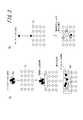
- (A) is a schematic diagram explaining the irradiation mechanism in the case of irradiating cluster ions
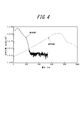
- (B) is a schematic diagram explaining the injection mechanism in the case of injecting monomer ions. It is a carbon concentration profile obtained by SIMS measurement in Reference Examples 1 and 2.
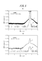
- (A) is the graph which combined the carbon concentration profile of the silicon epitaxial wafer and the Ni concentration profile after gettering ability evaluation about Example 1 and (B) about the comparative example 4.
- FIG. 1 is a schematic cross-sectional view of a semiconductor epitaxial wafer 100 obtained as a result of this manufacturing method.
- Examples of the semiconductor wafer 10 include a bulk single crystal wafer made of silicon, a compound semiconductor (GaAs, GaN, SiC) and having no epitaxial layer on the surface.
- a bulk single crystal silicon wafer is generally used.
- the semiconductor wafer 10 can use what sliced the single crystal silicon ingot grown by the Czochralski method (CZ method) and the floating zone melting method (FZ method) with the wire saw etc.
- CZ method Czochralski method
- FZ method floating zone melting method
- carbon and / or nitrogen may be added to obtain higher gettering ability.
- an arbitrary impurity dopant may be added to be n-type or p-type.
- the first embodiment shown in FIG. 1 is an example in which a bulk semiconductor wafer 12 having no epitaxial layer on the surface is used as the semiconductor wafer 10.
- an epitaxial semiconductor wafer in which a semiconductor epitaxial layer (first epitaxial layer) 14 is formed on the surface of the bulk semiconductor wafer 12 can be exemplified.
- a semiconductor epitaxial layer first epitaxial layer
- the silicon epitaxial layer can be formed under general conditions by a CVD (Chemical Vapor Deposition) method.
- the first epitaxial layer 14 preferably has a thickness in the range of 0.1 to 10 ⁇ m, and more preferably in the range of 0.2 to 5 ⁇ m.
- 10 is irradiated with cluster ions 16 to form a modified layer 18 made of constituent elements of cluster ions 16 on the surface 10A of the semiconductor wafer (the surface of the first epitaxial layer 14 in this embodiment) (FIG. 2 (A) to (C)), and second heat treatment (recovery heat treatment) is performed on the semiconductor wafer 10 so that the haze level of the surface 10A of the semiconductor wafer is 0.20 ppm or less.
- FIG. 2E is a schematic cross-sectional view of a semiconductor epitaxial wafer 200 obtained as a result of this manufacturing method.
- the modified layer 18 formed as a result of irradiating the cluster ions 16 is a region where the constituent elements of the cluster ions 16 are locally present as a solid solution in the interstitial positions or substitution positions of crystals on the surface of the semiconductor wafer. Work as a gettering site. The reason is presumed as follows. That is, elements such as carbon and boron irradiated in the form of cluster ions are localized at a high density in the substitution position / interstitial position of the silicon single crystal.
- the cluster ions 16 are irradiated in the present invention, higher gettering ability can be obtained as compared with the case of injecting monomer ions. Therefore, it becomes possible to manufacture the semiconductor epitaxial wafers 100 and 200 having higher gettering ability, and the back-illuminated solid-state imaging device manufactured from the semiconductor epitaxial wafers 100 and 200 obtained by this manufacturing method has white scratches compared to the conventional case. Suppression of defect generation can be expected.
- cluster ions mean ions that are ionized by applying a positive charge or a negative charge to a cluster formed by aggregating a plurality of atoms or molecules.
- a cluster is a massive group in which a plurality (usually about 2 to 2000) of atoms or molecules are bonded to each other.
- the present inventors consider the action of obtaining high gettering ability by irradiating cluster ions as follows.
- the monomer ions are implanted into a silicon wafer, as shown in FIG. 3B, the monomer ions are blown off silicon atoms constituting the silicon wafer and implanted at a predetermined depth in the silicon wafer.
- the implantation depth depends on the type of constituent elements of the implanted ions and the acceleration voltage of the ions.
- the carbon concentration profile in the depth direction of the silicon wafer is relatively broad, and the region where the implanted carbon exists is approximately 0.5 to 1 ⁇ m.
- lighter elements are implanted deeper, that is, implanted at different positions according to the mass of each element, so the concentration profile of the implanted elements becomes broader. .
- the cluster ions 16 are instantaneously 1350 to 1400 with the energy when irradiated to the silicon wafer. It becomes a high temperature of about °C and silicon melts. Thereafter, the silicon is rapidly cooled, and carbon and boron are dissolved in the vicinity of the surface in the silicon wafer. That is, the “modified layer” in the present specification means a layer in which constituent elements of ions to be irradiated are dissolved in crystal interstitial positions or substitution positions on the surface of the semiconductor wafer.
- the concentration profile of carbon and boron in the depth direction of the silicon wafer depends on the acceleration voltage and cluster size of cluster ions, but is sharper than that of monomer ions, and the irradiated carbon and boron exist locally.
- the thickness of the region (that is, the modified layer) is approximately 500 nm or less (for example, about 50 to 400 nm). Note that the elements irradiated in the form of cluster ions undergo some thermal diffusion during the formation process of the epitaxial layer 20. For this reason, in the concentration profile of carbon and boron after the formation of the epitaxial layer 20, broad diffusion regions are formed on both sides of the peak where these elements exist locally. However, the thickness of the modified layer does not change greatly (see FIG. 5A described later).
- the carbon and boron precipitation regions can be locally and highly concentrated. Further, since the modified layer 18 is formed in the vicinity of the surface of the silicon wafer, closer gettering is possible. As a result, it is considered that a higher gettering ability can be obtained than when monomer ions are implanted.
- the cluster ion form there is an advantage that a plurality of types of ions can be irradiated simultaneously by a single cluster ion irradiation treatment.
- Monomer ions are generally implanted at an acceleration voltage of about 150 to 2000 keV. Since each ion collides with a silicon atom with its energy, the crystallinity of the surface layer portion of the silicon wafer into which the monomer ions are implanted is greatly disturbed. Therefore, even if heat treatment (recovery heat treatment) for recovering the disordered crystallinity after ion implantation is performed, the recovery rate of the haze level on the surface of the epitaxial layer formed thereafter is low.
- cluster ions are generally irradiated at an acceleration voltage of about 10 to 100 keV / Cluster.
- a cluster is an aggregate of a plurality of atoms or molecules, it is implanted with a small energy per atom or molecule. Can do. Therefore, the damage given to the crystal of the semiconductor wafer surface layer is small.
- the cluster ion irradiation does not disturb the crystallinity of the surface layer portion of the semiconductor wafer than the monomer ion implantation.
- the crystallinity of the outermost surface of the semiconductor wafer may be disturbed depending on the size and dose of cluster ions used, and the haze level on the surface of the epitaxial layer may increase. Even in such a case, the haze level on the surface of the epitaxial layer 20 is sufficiently reduced by performing the recovery heat treatment under a predetermined condition in the second step after the first step and then performing the third step of epitaxially growing the epitaxial layer 20. Can do.
- the cluster ion 16 has various clusters depending on the bonding mode, and can be generated by a known method as described in the following document, for example.
- a method for generating a gas cluster beam (1) JP-A-9-41138, (2) JP-A-4-354865, and as an ion beam generating method, (1) charged particle beam engineering: Junzo Ishikawa: ISBN978 -4-339-00734-3: Corona, (2) Electron and ion beam engineering: The Institute of Electrical Engineers of Japan: ISBN4-88686-217-9: Ohm, (3) Cluster ion beam fundamentals and applications: ISBN4-526-05765 -7: Nikkan Kogyo Shimbun.
- a Nielsen ion source or a Kaufman ion source is used to generate positively charged cluster ions
- a large current negative ion source using a volume generation method is used to generate negatively charged cluster ions. It is done.
- the irradiation element is not particularly limited, and examples thereof include carbon, boron, phosphorus, and arsenic.
- the cluster ions preferably contain carbon as a constituent element. Since the carbon atom at the lattice position has a smaller covalent bond radius than that of the silicon single crystal, a contraction field of the silicon crystal lattice is formed, so that the gettering ability to attract impurities between the lattices is high.
- two or more elements including carbon are included as constituent elements. This is because the types of metals that can be efficiently gettered differ depending on the types of deposited elements, so that two or more types of elements can be dissolved to cope with a wider range of metal contamination. For example, in the case of carbon, nickel can be efficiently gettered, and in the case of boron, copper and iron can be efficiently gettered.
- the compound to be ionized is not particularly limited, and ethane, methane, carbon dioxide (CO 2 ) and the like can be used as the ionizable carbon source compound, and diborane as the ionizable boron source compound.
- Decaborane (B 10 H 14 ) or the like can be used.
- a gas in which benzyl and decaborane are mixed is used as a material gas
- a hydrogen compound cluster in which carbon, boron, and hydrogen are aggregated can be generated.
- cyclohexane (C 6 H 12 ) is used as a material, cluster ions composed of carbon and hydrogen can be generated.
- the carbon source compound it is particularly preferable to use a cluster C n H m (3 ⁇ n ⁇ 16, 3 ⁇ m ⁇ 10) formed from pyrene (C 16 H 10 ), dibenzyl (C 14 H 14 ) or the like. This is because a small-sized cluster ion beam can be easily formed.
- cluster size means the number of atoms or molecules constituting one cluster.
- the concentration profile of the constituent elements in the modified layer 18 in the depth direction is within a range of 150 nm or less from the surface 10A of the semiconductor wafer 10.
- the cluster ions 16 are irradiated so that the peak of is located.
- the “concentration profile in the depth direction of the constituent element” means not a total but a profile of each single element when the constituent element includes two or more elements. .
- the acceleration voltage per carbon atom is 0 keV / atom and 50 keV / atom or less, preferably 40 keV / atom or less.
- the cluster size is 2 to 100, preferably 60 or less, more preferably 50 or less.
- the cluster size can be adjusted by adjusting the gas pressure of the gas ejected from the nozzle, the pressure of the vacuum vessel, the voltage applied to the filament during ionization, and the like.
- the cluster size can be obtained by obtaining a cluster number distribution by mass spectrometry using a quadrupole high-frequency electric field or time-of-flight mass spectrometry and taking an average value of the number of clusters.
- the dose amount of cluster ions can be adjusted by controlling the ion irradiation time.
- the carbon dose of the cluster ions is preferably 1 ⁇ 10 13 to 1 ⁇ 10 16 atoms / cm 2 . If it is less than 1 ⁇ 10 13 atoms / cm 2 , the gettering ability may not be sufficiently obtained, and if it exceeds 1 ⁇ 10 16 atoms / cm 2 , the epitaxial surface may be greatly damaged. It is.
- the carbon dose of the cluster ions is preferably 2.0 ⁇ 10 14 atoms / cm 2 or more. In this case, since damage to the crystal of the semiconductor wafer is increased, the effect of crystallinity recovery by the recovery heat treatment becomes more effective.
- Another characteristic step of the present invention is a second step in which a heat treatment for recovery of crystallinity (recovery heat treatment) is performed on the semiconductor wafer 10 so that the haze level of the semiconductor wafer surface 10A is 0.20 ppm or less ( FIG. 1C and FIG. 2D). If the haze level of the surface 10A of the semiconductor wafer is 0.20 ppm or less, the epitaxial layer surface of the semiconductor epitaxial wafer can be 0.30 ppm or less by forming the epitaxial layer 20 in the subsequent third step. .
- the haze level is an index of the surface roughness of the semiconductor wafer.
- fogging called haze is likely to occur on the surface of the epitaxial layer, making it difficult to measure LPD (Light Point Defects) using a particle counter. This indicator is used because the quality of the wafer may not be guaranteed.
- the haze level is obtained as a ratio (ppm) of total scattered light to incident light when measuring the surface scattered light of the light (mainly laser light) irradiated on the wafer surface, and can be measured by any method. .
- the wafer surface is observed in the DWN mode (Dark Field Wide Wide Normal mode: dark field / wide / normal incidence mode), and the obtained haze value is obtained.
- DWN mode Dark Field Wide Wide Normal mode: dark field / wide / normal incidence mode
- the haze level increases as the surface roughness increases.
- a hydrogen bake process that is performed prior to epitaxial growth is performed in an epitaxial growth apparatus for forming the epitaxial layer 20.
- the crystallinity of the semiconductor wafer 10 can be recovered.
- the general conditions for the hydrogen baking are as follows: the inside of the epitaxial growth apparatus is in a hydrogen atmosphere, and the silicon wafer 10 is placed in the furnace at a furnace temperature of 600 ° C. or higher and 900 ° C. or lower. The temperature is raised to a temperature range of 1100 ° C. or more and 1200 ° C.
- the heat treatment more than this general hydrogen baking treatment is actively performed.
- the recovery heat treatment conditions in the case of also serving as a hydrogen baking treatment can be such that the holding temperature and holding time are 1100 to 1200 ° C. for 1 minute or more, respectively, and the holding time is more preferably 2 minutes or more.
- the upper limit of heat processing time is not specifically limited, For example, it can be 10 minutes.
- a heating apparatus separate from the epitaxial apparatus, such as RTA / RTO (Rapid Thermal Oxidation) and a batch heat treatment apparatus (vertical heat treatment apparatus, horizontal heat treatment apparatus).
- Recovery heat treatment can be performed using
- the recovery heat treatment can be performed under a recovery heat treatment condition of 900 to 1200 ° C. and 10 seconds to 1 hour.
- the heat treatment temperature is set to 900 to 1200 ° C. or less because if the temperature is less than 900 ° C., it is difficult to obtain the crystallinity recovery effect.
- it exceeds 1200 ° C. slip caused by the heat treatment at a high temperature This is because the heat load on the apparatus increases.
- the heat treatment time is set to 10 seconds to 1 hour because a recovery effect is difficult to be obtained if the heat treatment time is less than 10 seconds.
- the heat treatment time exceeds 1 hour, the productivity is lowered and the heat load on the apparatus is large. It is to become.
- the semiconductor wafer 10 is transferred to the epitaxial growth apparatus, and the subsequent third step is performed. Note that when the carbon dose of the cluster ions is 1.0 ⁇ 10 15 atoms / cm 2 or more, the time required for the recovery heat treatment becomes long. Therefore, the recovery heat treatment is performed before being transferred into the epitaxial growth apparatus. It is more preferable.
- the second epitaxial layer 20 formed on the modified layer 18 includes a silicon epitaxial layer, and can be formed under general conditions.
- a source gas such as dichlorosilane or trichlorosilane is introduced into the chamber using hydrogen as a carrier gas, and the growth temperature varies depending on the source gas used, but the semiconductor is formed by a CVD method at a temperature in the range of about 1000 to 1200 ° C. It can be epitaxially grown on the wafer 10.
- the epitaxial layer 20 preferably has a thickness in the range of 1 to 15 ⁇ m.
- the resistivity of the second epitaxial layer 20 may change due to the out-diffusion of the dopant from the semiconductor wafer 10, and if it exceeds 15 ⁇ m, the spectral sensitivity characteristics of the solid-state imaging device are affected. This is because there is a risk of occurrence.
- the second epitaxial layer 20 becomes a device layer for manufacturing a back-illuminated solid-state imaging device.
- the second embodiment shown in FIG. 2 is characterized in that the cluster ion irradiation is performed not on the bulk semiconductor wafer 12 but on the first epitaxial layer 14.
- a bulk semiconductor wafer has an oxygen concentration about two orders of magnitude higher than that of an epitaxial layer. Therefore, in the modified layer formed in the bulk semiconductor wafer, more oxygen is diffused than the modified layer formed in the epitaxial layer, and much oxygen is captured. The trapped oxygen is re-emitted from the capture site during the device process and diffuses into the active region of the device, forming point defects, thus adversely affecting the electrical properties of the device. Therefore, an important design condition in the device process is to irradiate an epitaxial layer having a low solid solution oxygen concentration with cluster ions and form a gettering layer in the epitaxial layer in which the influence of oxygen diffusion can be almost ignored.
- semiconductor epitaxial wafers 100 and 200 obtained by the above manufacturing method will be described.
- the semiconductor epitaxial wafer 100 according to the first embodiment and the semiconductor epitaxial wafer 200 according to the second embodiment are formed on the semiconductor wafer 10 and the surface of the semiconductor wafer 10 as shown in FIG. 1 (D) and FIG. 2 (E).
- the half width W of the concentration profile in the depth direction of the predetermined element in the modified layer 18 is 100 nm or less
- the haze level on the surface of the epitaxial layer 20 is 0.30 ppm or less.
- the precipitation region of the elements constituting the cluster ions can be locally and highly concentrated as compared with the monomer ion implantation, so that the half width W is set to 100 nm or less. Became possible.
- the lower limit can be set to 10 nm.
- the “concentration profile in the depth direction” in this specification means a concentration distribution in the depth direction measured by secondary ion mass spectrometry (SIMS: Secondary Ion Mass Spectrometry).
- SIMS Secondary Ion Mass Spectrometry
- the “half-value width of the concentration profile in the depth direction of the predetermined element” is calculated in consideration of measurement accuracy when the thickness of the epitaxial layer exceeds 1 ⁇ m. The half-value width when the concentration profile of the predetermined element is measured.
- the epitaxial layer 20 is formed after the recovery heat treatment is performed so that the haze level of the surface 10A of the semiconductor wafer 10 is 0.20 ppm or less after the cluster ion irradiation.
- the level can be reduced to 0.30 ppm or less.
- the measurement of the haze level on the surface of the semiconductor epitaxial wafer can be performed in the same manner as the measurement of the haze level of the semiconductor wafer described above.
- the predetermined element is not particularly limited as long as it is an element other than the main material of the semiconductor wafer (silicon in the case of a silicon wafer), but it is preferable to use carbon or two or more elements containing carbon as described above. It is.
- the peak of the concentration profile in the modified layer 18 is located in the semiconductor epitaxial wafers 100 and 200 within the depth of 150 nm or less from the surface of the semiconductor wafer 10. Is preferred. Further, the peak concentration of the concentration profile is preferably 1 ⁇ 10 15 atoms / cm 3 or more, more preferably in the range of 1 ⁇ 10 17 to 1 ⁇ 10 22 atoms / cm 3 , and 1 ⁇ 10 19 to 1 More preferably within the range of ⁇ 10 21 atoms / cm 3 .
- the haze level on the surface of the epitaxial layer 20 is 0.30 ppm or less, more preferably 0.26 ppm or less, and the lower limit can be set to 0.05 ppm.
- the thickness in the depth direction of the modified layer 18 can be approximately in the range of 30 to 400 nm.
- metal gettering can be further suppressed by exhibiting higher gettering ability than the conventional one, and the haze level of the epitaxial layer surface is 0.30 ppm or less. It can be.
- a method for manufacturing a solid-state imaging device includes a solid-state imaging device on the epitaxial wafer manufactured by the manufacturing method described above or the epitaxial layer 20 positioned on the surface of the epitaxial wafer, that is, the semiconductor epitaxial wafers 100 and 200. It is characterized by forming.
- the solid-state imaging device obtained by this manufacturing method can reduce the influence of heavy metal contamination that occurs during each process of the manufacturing process as compared with the conventional method, and can sufficiently suppress the occurrence of white defect as compared with the conventional method.
- two epitaxial layers may be formed on the semiconductor wafer 10.
- C 5 H 5 clusters are generated from dibenzyl (C 14 H 14 ), and the dose amount is 1.2 ⁇ 10 14 Clusters /
- the silicon wafer was irradiated under irradiation conditions of cm 2 (carbon dose amount 6.0 ⁇ 10 14 atoms / cm 2 ) and 14.8 keV / atom per carbon atom.
- Reference Example 2 For the same silicon wafer as in Reference Example 1, instead of cluster ion irradiation, carbon monomer ions are generated using CO 2 as a material gas, a dose amount of 1.2 ⁇ 10 14 atoms / cm 2 , an acceleration voltage of 300 keV / The silicon wafer was irradiated under the same conditions as in Reference Example 1 except that the atom conditions were used.
- Example 1 An n-type silicon wafer (diameter: 300 mm, thickness: 725 ⁇ m, dopant type: phosphorus, dopant concentration: 4 ⁇ 10 14 atoms / cm 3 ) obtained from CZ single crystal was prepared.
- a C 5 H 5 cluster is generated from dibenzyl (C 14 H 14 ) using a cluster ion generator (manufactured by Nissin Ion Equipment Co., Ltd., model number: CLARIS), and a dose of 1.2 ⁇ 10 14 Clusters /
- the silicon wafer was irradiated under irradiation conditions of cm 2 (carbon dose amount 6.0 ⁇ 10 14 atoms / cm 2 ) and 14.8 keV / atom per carbon atom. After that, the silicon wafer is transferred into an epitaxial growth apparatus (Applied Materials Co., Ltd.), and heat treatment that doubles hydrogen bake treatment at a temperature of 1130 ° C.
- a silicon epitaxial layer (thickness: 7 ⁇ m, dopant type: phosphorus, dopant concentration: 1 ⁇ 10 6) is formed on the silicon wafer by CVD at 1000 to 1150 ° C. using hydrogen as a carrier gas and trichlorosilane as a source gas. 15 atoms / cm 3 ) was epitaxially grown to obtain a silicon epitaxial wafer according to the present invention.
- Example 2 Instead of recovery heat treatment that also serves as hydrogen baking in the epitaxial device, before transporting the silicon wafer to the epitaxial growth device, an RTA device (manufactured by Matson Thermal Product Co., Ltd.) is used under the conditions of 900 ° C. and 10 seconds.
- the present invention was carried out under the same conditions as in Example 1 except that a recovery heat treatment was performed, and then the film was transported into an epitaxial growth apparatus and subjected to a hydrogen baking process at a temperature of 1130 ° C. for 30 seconds to grow an epitaxial layer.
- a silicon epitaxial wafer according to the above was prepared.
- Example 3 A silicon epitaxial wafer according to the present invention was produced in the same manner as in Example 1 except that the irradiation conditions of cluster ions were changed to those shown in Table 1.
- Example 4 A silicon epitaxial wafer according to the present invention was produced in the same manner as in Example 2 except that the irradiation conditions of cluster ions were changed to those shown in Table 1.
- Comparative Examples 3 and 4 The silicon according to the comparative example is the same as the comparative example 1 except that carbon monomer ions are implanted under the conditions described in Table 1 instead of the cluster ion irradiation and the recovery heat treatment conditions are the conditions described in Table 1. An epitaxial wafer was produced.
- SIMS Measurement As a representative example, SIMS measurement was performed on the silicon epitaxial wafers of Example 1 and Comparative Example 4, and the carbon concentration profiles shown in FIGS. 5A and 5B were obtained. The depth of the horizontal axis is zero on the surface of the epitaxial layer. Further, SIMS measurement was performed on the samples prepared in Examples 1 to 4 and Comparative Examples 1 to 4 after the epitaxial layer was thinned to 1 ⁇ m. Table 1 shows the half width, peak concentration, and peak position (peak depth from the surface excluding the epitaxial layer) of the carbon concentration profile obtained at this time.
- Example 1 (2) Evaluation of gettering ability
- the surface of the silicon epitaxial wafer of each sample prepared in Example 1 and Comparative Example 4 was intentionally formed with Ni contamination liquid (1.0 ⁇ 10 12 / cm 2 ) using a spin coat contamination method. Subsequently, a heat treatment was performed at 900 ° C. for 30 minutes. Thereafter, SIMS measurement was performed.
- the Ni concentration profiles for Example 1 and Comparative Example 4 are shown together with the carbon concentration profiles (FIGS. 5A and 5B).
- Table 1 shows the results of gettering ability evaluation for other examples and comparative examples. The peak concentrations of the Ni concentration profile were classified as follows and used as evaluation criteria.
- Example 1 (Consideration of evaluation results) 5A and 5B, the modified layer in which carbon is locally dissolved at a high concentration is formed in Example 1 by cluster ion irradiation as compared with Comparative Example 4 in which monomer ion implantation is performed.
- Example 1 and Comparative Example 4 from the Ni concentration profile, in Example 1, the modified layer formed by cluster ion irradiation captures a large amount of Ni and exhibits high gettering ability.
- Table 1 it can be seen that Examples 1 to 4 and Comparative Examples 1 and 2 irradiated with cluster ions all have a full width at half maximum of 100 nm or less, and all have sufficient gettering ability.
- the haze level of the silicon wafer surface is recovered to 0.20 ppm or less before forming the epitaxial layer. It was found that heat treatment was necessary. Further, comparing Comparative Example 3 with Comparative Example 4, it can be seen that the haze level is recovered by the recovery heat treatment even in the case of monomer ion implantation, but the recovery effect is slight compared with the case of irradiation with cluster ions. .
- a high-quality solid-state imaging device can be formed from the epitaxial wafer.
Landscapes
- Chemical & Material Sciences (AREA)
- Chemical Kinetics & Catalysis (AREA)
- Engineering & Computer Science (AREA)
- Materials Engineering (AREA)
- Metallurgy (AREA)
- Organic Chemistry (AREA)
- General Chemical & Material Sciences (AREA)
- Mechanical Engineering (AREA)
- Crystallography & Structural Chemistry (AREA)
- Physics & Mathematics (AREA)
- Health & Medical Sciences (AREA)
- Optics & Photonics (AREA)
- Toxicology (AREA)
- Inorganic Chemistry (AREA)
- Recrystallisation Techniques (AREA)
- Solid State Image Pick-Up Elements (AREA)
- Chemical Vapour Deposition (AREA)
- Spectroscopy & Molecular Physics (AREA)
Abstract
Description
すなわち、本発明の半導体エピタキシャルウェーハの製造方法は、半導体ウェーハにクラスターイオンを照射して、該半導体ウェーハの表面に、前記クラスターイオンの構成元素からなる改質層を形成する第1工程と、該第1工程の後、前記半導体ウェーハ表面のヘイズレベルが0.20ppm以下となるように、結晶性回復のための熱処理を前記半導体ウェーハに対して行なう第2工程と、該第2工程の後、前記半導体ウェーハの改質層上にエピタキシャル層を形成する第3工程と、を有することを特徴とする。
本発明の第1実施形態による半導体エピタキシャルウェーハ100の製造方法は、図1に示すように、半導体ウェーハ10にクラスターイオン16を照射して、半導体ウェーハ10の表面10Aに、このクラスターイオン16の構成元素からなる改質層18を形成する第1工程(図1(A),(B))と、半導体ウェーハ10の表面10Aのヘイズレベルが0.20ppm以下となるように、結晶性回復のための熱処理(回復熱処理)を半導体ウェーハ10に対して行なう第2工程(図1(C))と、半導体ウェーハ10の改質層18上にエピタキシャル層20を形成する第3工程(図1(D))と、を有することを特徴とする。図1(D)は、この製造方法の結果得られた半導体エピタキシャルウェーハ100の模式断面図である。
次に、上記製造方法により得られる半導体エピタキシャルウェーハ100,200について説明する。第1実施形態による半導体エピタキシャルウェーハ100および第2実施形態による半導体エピタキシャルウェーハ200は、図1(D)および図2(E)に示すように、半導体ウェーハ10と、この半導体ウェーハ10の表面に形成され、半導体ウェーハ10中に固溶した所定元素からなる改質層18と、この改質層18上のエピタキシャル層20と、を有する。そして、いずれにおいても改質層18における所定元素の深さ方向の濃度プロファイルの半値幅Wが100nm以下であり、かつエピタキシャル層20表面のヘイズレベルが0.30ppm以下であることを特徴とする。
本発明の実施形態による固体撮像素子の製造方法は、上記の製造方法で製造されたエピタキシャルウェーハまたは上記のエピタキシャルウェーハ、すなわち半導体エピタキシャルウェーハ100,200の表面に位置するエピタキシャル層20に、固体撮像素子を形成することを特徴とする。この製造方法により得られる固体撮像素子は、従来に比べ製造工程の各処理中で発生する重金属汚染の影響を低減でき、従来に比べ白傷欠陥の発生を十分に抑制することができる。
まず、クラスターイオン照射とモノマーイオン注入の相違を明らかにするため、以下の実験を行った。
CZ単結晶から得た、n型シリコンウェーハ(直径:300mm、厚さ:725μm、ドーパント:リン、ドーパント濃度:4×10¹⁴atoms/cm3)を用意した。次に、クラスターイオン発生装置(日新イオン機器社製、型番:CLARIS)を用いて、ジベンジル(C14H14)よりC5H5クラスターを生成し、ドーズ量1.2×1014Clusters/cm2(炭素のドーズ量6.0×1014atoms/cm2)、炭素1原子あたり14.8keV/atomの照射条件でシリコンウェーハに照射した。
参考例1と同じシリコンウェーハに対して、クラスターイオン照射に替えて、CO2を材料ガスとして、炭素のモノマーイオンを生成し、ドーズ量1.2×10¹⁴atoms/cm2、加速電圧300keV/atomの条件とした以外は、参考例1と同じ条件で、シリコンウェーハに照射した。
上記参考例1,2で作製したサンプルについて、SIMSにより測定を行い、図4に示す炭素の濃度プロファイルを得た。なお、横軸の深さはシリコンウェーハ表面をゼロとしている。この図4から明らかなように、クラスターイオン照射をした参考例1では、炭素濃度プロファイルがシャープであるが、モノマーイオン注入をした参考例2では、炭素濃度プロファイルがブロードである。また、参考例2に比べて参考例1では、炭素の濃度プロファイルのピーク濃度が高く、ピーク位置もよりシリコンウェーハ表面近傍に位置している。このことから、エピタキシャル層形成後も、炭素の濃度プロファイルの傾向は同様となることが推定される。
CZ単結晶から得たn型シリコンウェーハ(直径:300mm、厚さ:725μm、ドーパント種類:燐、ドーパント濃度:4×10¹⁴atoms/cm3)を用意した。次に、クラスターイオン発生装置(日新イオン機器社製、型番:CLARIS)を用いて、ジベンジル(C14H14)よりC5H5クラスターを生成し、ドーズ量1.2×1014Clusters/cm2(炭素のドーズ量6.0×1014atoms/cm2)、炭素1原子あたり14.8keV/atomの照射条件でシリコンウェーハに照射した。その後、シリコンウェーハをエピタキシャル成長装置(アプライドマテリアルズ社製)内に搬送し、クラスターイオン照射により乱れた結晶性の回復熱処理として、装置内で1130℃の温度で2分の水素ベーク処理を兼ねた熱処理を施した後、水素をキャリアガス、トリクロロシランをソースガスとして1000~1150℃でCVD法により、シリコンウェーハ上にシリコンのエピタキシャル層(厚さ:7μm、ドーパント種類:燐、ドーパント濃度:1×1015atoms/cm3)をエピタキシャル成長させ、本発明に従うシリコンエピタキシャルウェーハとした。
エピタキシャル装置内での水素ベーク処理を兼ねた回復熱処理に替えて、シリコンウェーハをエピタキシャル成長装置に搬送する前に、RTA装置(マトソンサーマルプロダクト社製)を使用して、900℃,10秒の条件で回復熱処理を施し、その後エピタキシャル成長装置内に搬送して、装置内で1130℃の温度で30秒の水素ベーク処理を施してエピタキシャル層を成長させた以外は、実施例1と同じ条件で、本発明に従うシリコンエピタキシャルウェーハを作製した。
クラスターイオンの照射条件を表1に記載の条件とした以外は、実施例1と同様にして本発明に従うシリコンエピタキシャルウェーハを作製した。
クラスターイオンの照射条件を表1に記載の条件とした以外は、実施例2と同様にして本発明に従うシリコンエピタキシャルウェーハを作製した。
クラスターイオンの照射条件を表1に記載のとおりとし、回復熱処理工程を行わなかったこと以外は、実施例2と同様にして比較例にかかるシリコンエピタキシャルウェーハを作製した。
クラスターイオン照射に替えて、表1に記載の条件で炭素のモノマーイオンを注入し、さらに回復熱処理条件を表1に記載の条件とした以外は、比較例1と同様にして比較例にかかるシリコンエピタキシャルウェーハを作製した。
上記実施例および比較例で作製した各サンプルについて評価を行った。評価方法を以下に示す。
代表例として、実施例1および比較例4のシリコンエピタキシャルウェーハについてSIMS測定を行い、図5(A),(B)に示す炭素の濃度プロファイルを得た。なお、横軸の深さはエピタキシャル層の表面をゼロとしている。さらに、実施例1~4および比較例1~4で作製した各サンプルについて、エピタキシャル層を1μmまで薄膜化した後にSIMS測定を行った。このとき得られた炭素の濃度プロファイルの半値幅、ピーク濃度、およびピーク位置(エピタキシャル層を除いた表面からのピーク深さ)を表1に示す。
実施例1および比較例4で作製した各サンプルのシリコンエピタキシャルウェーハ表面を、Ni汚染液(1.0×10¹²/cm2)で、スピンコート汚染法を用いて故意に汚染し、引き続き900℃、30分の熱処理を施した。その後、SIMS測定を行った。実施例1および比較例4についてのNi濃度プロファイルを、それぞれ炭素濃度プロファイルとともに示す(図5(A),(B))。他の実施例および比較例については、ゲッタリング能力評価の結果を表1に示す。なお、Ni濃度プロファイルのピーク濃度を以下のようにそれぞれ分類して、評価基準とした。
◎:1.0×10¹⁷atoms/cm3以上
○:5.0×10¹⁶atoms/cm3以上~1.0×1017atoms/cm3未満
△:5.0×10¹⁶atoms/cm3未満
実施例および比較例で作製した各サンプルについて、エピタキシャル層表面で観察されるエピタキシャル欠陥を評価した。表面欠陥検査装置(KLA-Tencor社製:Surfscan SP-2)を用いて、DWOモード(Dark Field Wide Obliqueモード:暗視野・ワイド・斜め入射モード)でエピタキシャル層表面を観察し、検出された欠陥部位を原子間力顕微鏡(AFM:Atomic Force Microscope)を用いて定点観察評価した。エピタキシャル層表面で観察されたCOP(Crystal originated particles)を起点とした積層欠陥(SF:Staking Fault)の個数を測定し、これをエピタキシャル欠陥として評価した。エピタキシャル欠陥の評価結果を表1に示す。なお、評価基準は以下のとおりである。
◎:2個/ウェーハ以下
○:2個/ウェーハ超~10個/ウェーハ以下
△:10個/ウェーハ超~50個/ウェーハ以下
×:50個/ウェーハ超
実施例および比較例で作製した各サンプルについて、KLA-Tencor社製:Surfscan SP-1を用い、DWNモードでエピタキシャル層形成前のシリコンウェーハ表面およびエピタキシャル形成後のエピタキシャル層表面をそれぞれ観察し、得られたヘイズ値の平均値をヘイズレベルとして評価した。ヘイズレベルの評価結果を表1に示す。なお、実施例1,3のクラスターイオン照射後かつエピタキシャル層形成前におけるシリコンウェーハ表面のヘイズレベルについては、水素ベークを模擬した回復熱処理を行ったときのヘイズレベルを測定したものである。

図5(A),(B)から、クラスターイオン照射により、実施例1では、モノマーイオン注入を施した比較例4と比べて、炭素が局所的かつ高濃度に固溶した改質層が形成されることがわかる。さらに、Niの濃度プロファイルから、実施例1と比較例4とを比較すると、実施例1ではクラスターイオン照射により形成された改質層が多量のNiを捕獲して、高いゲッタリング能力を発揮していることがわかる。また、表1に示すとおり、クラスターイオン照射した実施例1~4および比較例1,2は、全て半値幅が100nm以下であり、全て十分なゲッタリング能力を備えていることがわかる。一方、モノマーイオン注入した比較例3,4は、いずれも半値幅が100nm超であり、ゲッタリング能力が不足している。このように、クラスターイオンを照射した実施例1~4および比較例1,2は、モノマーイオンを注入した比較例3,4に比べ、炭素濃度プロファイルの半値幅が小さくなるために、より高いゲッタリング能力を得ることができていると言える。
10A 半導体ウェーハの表面
12 バルク半導体ウェーハ
14 第1エピタキシャル層
16 クラスターイオン
18 改質層
20 (第2)エピタキシャル層
100 半導体エピタキシャルウェーハ
200 半導体エピタキシャルウェーハ
Claims (14)
- 半導体ウェーハにクラスターイオンを照射して、該半導体ウェーハの表面に、前記クラスターイオンの構成元素からなる改質層を形成する第1工程と、
該第1工程の後、前記半導体ウェーハ表面のヘイズレベルが0.20ppm以下となるように、結晶性回復のための熱処理を前記半導体ウェーハに対して行なう第2工程と、
該第2工程の後、前記半導体ウェーハの改質層上にエピタキシャル層を形成する第3工程と、
を有することを特徴とする半導体エピタキシャルウェーハの製造方法。 - 前記半導体ウェーハが、シリコンウェーハである請求項1に記載の半導体エピタキシャルウェーハの製造方法。
- 前記半導体ウェーハが、シリコンウェーハの表面にシリコンエピタキシャル層が形成されたエピタキシャルシリコンウェーハであり、前記第1工程において前記改質層は前記シリコンエピタキシャル層の表面に形成される請求項1に記載の半導体エピタキシャルウェーハの製造方法。
- 前記クラスターイオンが、構成元素として炭素を含む請求項1~3のいずれか1項に記載の半導体エピタキシャルウェーハの製造方法。
- 前記クラスターイオンが、構成元素として炭素を含む2種以上の元素を含む請求項4に記載の半導体エピタキシャルウェーハの製造方法。
- 前記クラスターイオンの炭素のドーズ量が2.0×10¹⁴atoms/cm2以上である請求項4または5に記載の半導体エピタキシャルウェーハの製造方法。
- 半導体ウェーハと、該半導体ウェーハの表面に形成された、該半導体ウェーハ中に固溶した所定元素からなる改質層と、該改質層上のエピタキシャル層と、を有し、
前記改質層における前記所定元素の深さ方向の濃度プロファイルの半値幅が100nm以下であり、前記エピタキシャル層表面のヘイズレベルが0.30ppm以下であることを特徴とする半導体エピタキシャルウェーハ。 - 前記半導体ウェーハが、シリコンウェーハである請求項7に記載の半導体エピタキシャルウェーハ。
- 前記半導体ウェーハが、シリコンウェーハの表面にシリコンエピタキシャル層が形成されたエピタキシャルシリコンウェーハであり、前記改質層は前記シリコンエピタキシャル層の表面に位置する請求項7に記載の半導体エピタキシャルウェーハ。
- 前記半導体ウェーハの表面からの深さが150nm以下の範囲内に、前記改質層における前記濃度プロファイルのピークが位置する請求項7~9のいずれか1項に記載の半導体エピタキシャルウェーハ。
- 前記改質層における前記濃度プロファイルのピーク濃度が、1×10¹⁵atoms/cm3以上である請求項7~10のいずれか1項に記載の半導体エピタキシャルウェーハ。
- 前記所定元素が炭素を含む請求項7~11のいずれか1項に記載の半導体エピタキシャルウェーハ。
- 前記所定元素が炭素を含む2種以上の元素を含む請求項12に記載の半導体エピタキシャルウェーハ。
- 請求項1~6のいずれか1項に記載の製造方法で製造されたエピタキシャルウェーハまたは請求項7~13のいずれか1項に記載のエピタキシャルウェーハの、表面に位置するエピタキシャル層に、固体撮像素子を形成することを特徴とする固体撮像素子の製造方法。
Priority Applications (6)
| Application Number | Priority Date | Filing Date | Title |
|---|---|---|---|
| DE112013005409.4T DE112013005409B4 (de) | 2012-11-13 | 2013-11-12 | Verfahren zur Herstellung von Halbleiter-Epitaxiewafern, Halbleiter-Epitaxiewafer, und Verfahren zur Herstellung von Festkörper-Bildsensorvorrichtungen |
| KR1020157013181A KR101687525B1 (ko) | 2012-11-13 | 2013-11-12 | 반도체 에피텍셜 웨이퍼의 제조 방법, 반도체 에피텍셜 웨이퍼, 및 고체 촬상 소자의 제조 방법 |
| KR1020167034485A KR101808685B1 (ko) | 2012-11-13 | 2013-11-12 | 반도체 에피텍셜 웨이퍼의 제조 방법, 반도체 에피텍셜 웨이퍼, 및 고체 촬상 소자의 제조 방법 |
| US14/442,367 US20160181312A1 (en) | 2012-11-13 | 2013-11-12 | Method of producing semiconductor epitaxial wafer, semiconductor epitaxial wafer, and method of producing solid-state image sensing device |
| CN201380059256.3A CN104823269B (zh) | 2012-11-13 | 2013-11-12 | 半导体外延晶片的制造方法、半导体外延晶片以及固体摄像元件的制造方法 |
| US16/717,763 US20200127044A1 (en) | 2012-11-13 | 2019-12-17 | Method for producing semiconductor epitaxial wafer, semiconductor epitaxial wafer, and method of producing solid-state image sensing device |
Applications Claiming Priority (2)
| Application Number | Priority Date | Filing Date | Title |
|---|---|---|---|
| JP2012249598A JP5799935B2 (ja) | 2012-11-13 | 2012-11-13 | 半導体エピタキシャルウェーハの製造方法、半導体エピタキシャルウェーハ、および固体撮像素子の製造方法 |
| JP2012-249598 | 2012-11-13 |
Related Child Applications (2)
| Application Number | Title | Priority Date | Filing Date |
|---|---|---|---|
| US14/442,367 A-371-Of-International US20160181312A1 (en) | 2012-11-13 | 2013-11-12 | Method of producing semiconductor epitaxial wafer, semiconductor epitaxial wafer, and method of producing solid-state image sensing device |
| US16/717,763 Continuation US20200127044A1 (en) | 2012-11-13 | 2019-12-17 | Method for producing semiconductor epitaxial wafer, semiconductor epitaxial wafer, and method of producing solid-state image sensing device |
Publications (1)
| Publication Number | Publication Date |
|---|---|
| WO2014076945A1 true WO2014076945A1 (ja) | 2014-05-22 |
Family
ID=50730877
Family Applications (1)
| Application Number | Title | Priority Date | Filing Date |
|---|---|---|---|
| PCT/JP2013/006661 Ceased WO2014076945A1 (ja) | 2012-11-13 | 2013-11-12 | 半導体エピタキシャルウェーハの製造方法、半導体エピタキシャルウェーハ、および固体撮像素子の製造方法 |
Country Status (7)
| Country | Link |
|---|---|
| US (2) | US20160181312A1 (ja) |
| JP (1) | JP5799935B2 (ja) |
| KR (2) | KR101687525B1 (ja) |
| CN (1) | CN104823269B (ja) |
| DE (1) | DE112013005409B4 (ja) |
| TW (1) | TWI515774B (ja) |
| WO (1) | WO2014076945A1 (ja) |
Cited By (1)
| Publication number | Priority date | Publication date | Assignee | Title |
|---|---|---|---|---|
| WO2017064908A1 (ja) * | 2015-10-13 | 2017-04-20 | 住友電気工業株式会社 | 炭化珪素エピタキシャル基板および炭化珪素半導体装置の製造方法 |
Families Citing this family (13)
| Publication number | Priority date | Publication date | Assignee | Title |
|---|---|---|---|---|
| JP6221928B2 (ja) * | 2014-05-13 | 2017-11-01 | 株式会社Sumco | 半導体エピタキシャルウェーハの製造方法および固体撮像素子の製造方法 |
| JP6539959B2 (ja) * | 2014-08-28 | 2019-07-10 | 株式会社Sumco | エピタキシャルシリコンウェーハおよびその製造方法、ならびに、固体撮像素子の製造方法 |
| JP6493104B2 (ja) * | 2015-09-03 | 2019-04-03 | 株式会社Sumco | 半導体エピタキシャルウェーハの製造方法、品質予測方法および品質評価方法 |
| JP6402703B2 (ja) * | 2015-11-17 | 2018-10-10 | 信越半導体株式会社 | 欠陥領域の判定方法 |
| JP6504082B2 (ja) * | 2016-02-29 | 2019-04-24 | 株式会社Sumco | 半導体エピタキシャルウェーハおよびその製造方法ならびに固体撮像素子の製造方法 |
| JP6724824B2 (ja) * | 2017-03-08 | 2020-07-15 | 株式会社Sumco | 半導体エピタキシャルウェーハの製造方法、品質予測方法および品質評価方法 |
| JP6787268B2 (ja) | 2017-07-20 | 2020-11-18 | 株式会社Sumco | 半導体エピタキシャルウェーハおよびその製造方法、ならびに固体撮像素子の製造方法 |
| WO2019167901A1 (ja) * | 2018-03-01 | 2019-09-06 | 株式会社Sumco | エピタキシャルシリコンウェーハの製造方法およびエピタキシャルシリコンウェーハ |
| JP6988843B2 (ja) * | 2019-02-22 | 2022-01-05 | 株式会社Sumco | 半導体エピタキシャルウェーハ及びその製造方法 |
| JP7415827B2 (ja) * | 2020-07-01 | 2024-01-17 | 信越半導体株式会社 | シリコンエピタキシャルウエーハ及びその製造方法 |
| CN114486926B (zh) * | 2021-12-30 | 2024-03-26 | 深圳瑞波光电子有限公司 | 半导体激光芯片失效分析方法 |
| WO2024176711A1 (ja) * | 2023-02-22 | 2024-08-29 | 株式会社Sumco | エピタキシャルシリコンウェーハ及びその製造方法、並びに半導体デバイスの製造方法 |
| CN117316798B (zh) * | 2023-09-28 | 2025-03-21 | 西安奕斯伟材料科技股份有限公司 | 确定产生外延缺陷的部件的方法、装置及介质 |
Citations (7)
| Publication number | Priority date | Publication date | Assignee | Title |
|---|---|---|---|---|
| JP2001139399A (ja) * | 1999-11-10 | 2001-05-22 | Shin Etsu Handotai Co Ltd | シリコンエピタキシャルウェーハの製造方法及びシリコンエピタキシャルウェーハ |
| JP2009518869A (ja) * | 2005-12-09 | 2009-05-07 | セムイクウィップ・インコーポレーテッド | 炭素クラスターの注入により半導体デバイスを製造するためのシステムおよび方法 |
| JP2009540531A (ja) * | 2006-06-13 | 2009-11-19 | セムイクウィップ・インコーポレーテッド | イオンビーム装置およびイオン注入方法 |
| JP2010040864A (ja) * | 2008-08-06 | 2010-02-18 | Sumco Corp | エピタキシャルシリコンウェーハ及びその製造方法 |
| JP2011151318A (ja) * | 2010-01-25 | 2011-08-04 | Renesas Electronics Corp | 半導体装置およびその製造方法 |
| JP2011253983A (ja) * | 2010-06-03 | 2011-12-15 | Disco Abrasive Syst Ltd | シリコンウェーハへのゲッタリング層付与方法 |
| JP2012059849A (ja) * | 2010-09-08 | 2012-03-22 | Shin Etsu Handotai Co Ltd | シリコンエピタキシャルウェーハおよびシリコンエピタキシャルウェーハの製造方法 |
Family Cites Families (14)
| Publication number | Priority date | Publication date | Assignee | Title |
|---|---|---|---|---|
| JPH05152304A (ja) * | 1991-11-29 | 1993-06-18 | Sony Corp | 半導体基板の製造方法 |
| JP3384506B2 (ja) * | 1993-03-30 | 2003-03-10 | ソニー株式会社 | 半導体基板の製造方法 |
| JPH1174276A (ja) * | 1997-08-27 | 1999-03-16 | Sumitomo Metal Ind Ltd | エピタキシャルシリコン半導体基板とその製造方法 |
| JP2003163216A (ja) * | 2001-09-12 | 2003-06-06 | Wacker Nsce Corp | エピタキシャルシリコンウエハおよびその製造方法 |
| JP2008294245A (ja) | 2007-05-25 | 2008-12-04 | Shin Etsu Handotai Co Ltd | エピタキシャルウェーハの製造方法およびエピタキシャルウェーハ |
| JP2008311418A (ja) | 2007-06-14 | 2008-12-25 | Shin Etsu Handotai Co Ltd | エピタキシャルウェーハおよびエピタキシャルウェーハの製造方法 |
| US8779462B2 (en) * | 2008-05-19 | 2014-07-15 | Infineon Technologies Ag | High-ohmic semiconductor substrate and a method of manufacturing the same |
| JP5099023B2 (ja) | 2009-01-27 | 2012-12-12 | 信越半導体株式会社 | エピタキシャルウエーハの製造方法及び固体撮像素子の製造方法 |
| JP5381304B2 (ja) * | 2009-05-08 | 2014-01-08 | 株式会社Sumco | シリコンエピタキシャルウェーハの製造方法 |
| JP2010283296A (ja) * | 2009-06-08 | 2010-12-16 | Sumco Corp | シリコンウェーハ及びその製造方法、並びに、半導体デバイスの製造方法 |
| WO2011004602A1 (ja) * | 2009-07-08 | 2011-01-13 | 株式会社Sumco | エピタキシャルウェーハおよびその製造方法 |
| US10181402B2 (en) * | 2010-08-23 | 2019-01-15 | Exogenesis Corporation | Method and apparatus for neutral beam processing based on gas cluster ion beam technology and articles produced thereby |
| US8648389B2 (en) * | 2011-06-08 | 2014-02-11 | Sumitomo Electric Industries, Ltd. | Semiconductor device with spacer layer between carrier traveling layer and carrier supplying layer |
| JP6127748B2 (ja) * | 2013-06-10 | 2017-05-17 | 株式会社Sumco | エピタキシャルウェーハの製造方法 |
-
2012
- 2012-11-13 JP JP2012249598A patent/JP5799935B2/ja active Active
-
2013
- 2013-11-12 US US14/442,367 patent/US20160181312A1/en not_active Abandoned
- 2013-11-12 TW TW102141070A patent/TWI515774B/zh active
- 2013-11-12 WO PCT/JP2013/006661 patent/WO2014076945A1/ja not_active Ceased
- 2013-11-12 KR KR1020157013181A patent/KR101687525B1/ko active Active
- 2013-11-12 DE DE112013005409.4T patent/DE112013005409B4/de active Active
- 2013-11-12 CN CN201380059256.3A patent/CN104823269B/zh active Active
- 2013-11-12 KR KR1020167034485A patent/KR101808685B1/ko active Active
-
2019
- 2019-12-17 US US16/717,763 patent/US20200127044A1/en not_active Abandoned
Patent Citations (7)
| Publication number | Priority date | Publication date | Assignee | Title |
|---|---|---|---|---|
| JP2001139399A (ja) * | 1999-11-10 | 2001-05-22 | Shin Etsu Handotai Co Ltd | シリコンエピタキシャルウェーハの製造方法及びシリコンエピタキシャルウェーハ |
| JP2009518869A (ja) * | 2005-12-09 | 2009-05-07 | セムイクウィップ・インコーポレーテッド | 炭素クラスターの注入により半導体デバイスを製造するためのシステムおよび方法 |
| JP2009540531A (ja) * | 2006-06-13 | 2009-11-19 | セムイクウィップ・インコーポレーテッド | イオンビーム装置およびイオン注入方法 |
| JP2010040864A (ja) * | 2008-08-06 | 2010-02-18 | Sumco Corp | エピタキシャルシリコンウェーハ及びその製造方法 |
| JP2011151318A (ja) * | 2010-01-25 | 2011-08-04 | Renesas Electronics Corp | 半導体装置およびその製造方法 |
| JP2011253983A (ja) * | 2010-06-03 | 2011-12-15 | Disco Abrasive Syst Ltd | シリコンウェーハへのゲッタリング層付与方法 |
| JP2012059849A (ja) * | 2010-09-08 | 2012-03-22 | Shin Etsu Handotai Co Ltd | シリコンエピタキシャルウェーハおよびシリコンエピタキシャルウェーハの製造方法 |
Cited By (4)
| Publication number | Priority date | Publication date | Assignee | Title |
|---|---|---|---|---|
| WO2017064908A1 (ja) * | 2015-10-13 | 2017-04-20 | 住友電気工業株式会社 | 炭化珪素エピタキシャル基板および炭化珪素半導体装置の製造方法 |
| JP2017076650A (ja) * | 2015-10-13 | 2017-04-20 | 住友電気工業株式会社 | 炭化珪素エピタキシャル基板および炭化珪素半導体装置の製造方法 |
| CN108028185A (zh) * | 2015-10-13 | 2018-05-11 | 住友电气工业株式会社 | 碳化硅外延基板及制造碳化硅半导体装置的方法 |
| US10396163B2 (en) | 2015-10-13 | 2019-08-27 | Sumitomo Electric Industries, Ltd. | Silicon carbide epitaxial substrate and method for manufacturing silicon carbide semiconductor device |
Also Published As
| Publication number | Publication date |
|---|---|
| JP5799935B2 (ja) | 2015-10-28 |
| KR101687525B1 (ko) | 2016-12-19 |
| CN104823269B (zh) | 2017-09-08 |
| DE112013005409T5 (de) | 2015-08-13 |
| KR20160148033A (ko) | 2016-12-23 |
| DE112013005409B4 (de) | 2024-02-01 |
| US20160181312A1 (en) | 2016-06-23 |
| JP2014099472A (ja) | 2014-05-29 |
| TW201426822A (zh) | 2014-07-01 |
| US20200127044A1 (en) | 2020-04-23 |
| KR20150065901A (ko) | 2015-06-15 |
| CN104823269A (zh) | 2015-08-05 |
| KR101808685B1 (ko) | 2017-12-13 |
| TWI515774B (zh) | 2016-01-01 |
Similar Documents
| Publication | Publication Date | Title |
|---|---|---|
| US20240297201A1 (en) | Method of producing semiconductor epitaxial wafer, semiconductor epitaxial wafer, and method of producing solid-state image sensing device | |
| JP5799935B2 (ja) | 半導体エピタキシャルウェーハの製造方法、半導体エピタキシャルウェーハ、および固体撮像素子の製造方法 | |
| JP5673811B2 (ja) | 半導体エピタキシャルウェーハの製造方法、半導体エピタキシャルウェーハ、および固体撮像素子の製造方法 | |
| JP5799936B2 (ja) | 半導体エピタキシャルウェーハの製造方法、半導体エピタキシャルウェーハ、および固体撮像素子の製造方法 | |
| WO2015104965A1 (ja) | 半導体エピタキシャルウェーハの製造方法、半導体エピタキシャルウェーハ、および固体撮像素子の製造方法 | |
| JP6107068B2 (ja) | エピタキシャルシリコンウェーハの製造方法、エピタキシャルシリコンウェーハ、および固体撮像素子の製造方法 | |
| TWI611482B (zh) | 半導體磊晶晶圓的製造方法及固體攝像元件的製造方法 | |
| JP6535432B2 (ja) | 半導体エピタキシャルウェーハの製造方法、半導体エピタキシャルウェーハ、および固体撮像素子の製造方法 | |
| JP6280301B2 (ja) | エピタキシャルシリコンウェーハの製造方法、エピタキシャルシリコンウェーハ、および固体撮像素子の製造方法 | |
| JP6221928B2 (ja) | 半導体エピタキシャルウェーハの製造方法および固体撮像素子の製造方法 | |
| JP6289805B2 (ja) | 半導体エピタキシャルウェーハの製造方法、半導体エピタキシャルウェーハ、および固体撮像素子の製造方法 | |
| JP6278592B2 (ja) | 半導体エピタキシャルウェーハの製造方法、半導体エピタキシャルウェーハ、および固体撮像素子の製造方法 | |
| JP6361779B2 (ja) | エピタキシャルシリコンウェーハの製造方法、エピタキシャルシリコンウェーハ、および固体撮像素子の製造方法 | |
| JP2017123477A (ja) | 半導体エピタキシャルウェーハの製造方法、半導体エピタキシャルウェーハ、および固体撮像素子の製造方法 | |
| JP2017175145A (ja) | 半導体エピタキシャルウェーハの製造方法、半導体エピタキシャルウェーハ、および固体撮像素子の製造方法 | |
| JP6318728B2 (ja) | 半導体エピタキシャルウェーハの製造方法、半導体エピタキシャルウェーハ、および固体撮像素子の製造方法 | |
| JP2017175143A (ja) | 半導体エピタキシャルウェーハの製造方法、半導体エピタキシャルウェーハ、および固体撮像素子の製造方法 | |
| JP2017183736A (ja) | 半導体エピタキシャルウェーハの製造方法、半導体エピタキシャルウェーハ、および固体撮像素子の製造方法 |
Legal Events
| Date | Code | Title | Description |
|---|---|---|---|
| 121 | Ep: the epo has been informed by wipo that ep was designated in this application |
Ref document number: 13855964 Country of ref document: EP Kind code of ref document: A1 |
|
| WWE | Wipo information: entry into national phase |
Ref document number: 14442367 Country of ref document: US |
|
| WWE | Wipo information: entry into national phase |
Ref document number: 112013005409 Country of ref document: DE Ref document number: 1120130054094 Country of ref document: DE |
|
| ENP | Entry into the national phase |
Ref document number: 20157013181 Country of ref document: KR Kind code of ref document: A |
|
| 122 | Ep: pct application non-entry in european phase |
Ref document number: 13855964 Country of ref document: EP Kind code of ref document: A1 |