WO2014069144A1 - 有機エレクトロルミネッセンス発光装置、及びその製造方法 - Google Patents
有機エレクトロルミネッセンス発光装置、及びその製造方法 Download PDFInfo
- Publication number
- WO2014069144A1 WO2014069144A1 PCT/JP2013/076690 JP2013076690W WO2014069144A1 WO 2014069144 A1 WO2014069144 A1 WO 2014069144A1 JP 2013076690 W JP2013076690 W JP 2013076690W WO 2014069144 A1 WO2014069144 A1 WO 2014069144A1
- Authority
- WO
- WIPO (PCT)
- Prior art keywords
- organic
- light emitting
- layer
- light
- emitting device
- Prior art date
Links
- 238000000034 method Methods 0.000 title claims abstract description 59
- 238000005401 electroluminescence Methods 0.000 title claims abstract description 29
- 238000004519 manufacturing process Methods 0.000 title claims abstract description 20
- 238000007789 sealing Methods 0.000 claims abstract description 162
- 239000000463 material Substances 0.000 claims abstract description 99
- 239000012044 organic layer Substances 0.000 claims abstract description 66
- 239000011229 interlayer Substances 0.000 claims abstract description 41
- 239000010410 layer Substances 0.000 claims description 247
- 239000000758 substrate Substances 0.000 claims description 90
- 229920005989 resin Polymers 0.000 claims description 55
- 239000011347 resin Substances 0.000 claims description 55
- 230000004888 barrier function Effects 0.000 claims description 28
- 230000008569 process Effects 0.000 claims description 17
- QVGXLLKOCUKJST-UHFFFAOYSA-N atomic oxygen Chemical compound [O] QVGXLLKOCUKJST-UHFFFAOYSA-N 0.000 claims description 12
- 239000001301 oxygen Substances 0.000 claims description 12
- 229910052760 oxygen Inorganic materials 0.000 claims description 12
- 239000002274 desiccant Substances 0.000 claims description 7
- 230000002745 absorbent Effects 0.000 claims description 5
- 239000002250 absorbent Substances 0.000 claims description 5
- 239000011368 organic material Substances 0.000 claims 2
- 239000010408 film Substances 0.000 description 37
- 238000002347 injection Methods 0.000 description 28
- 239000007924 injection Substances 0.000 description 28
- 239000002585 base Substances 0.000 description 25
- 230000005525 hole transport Effects 0.000 description 24
- -1 polymetaxylylene Polymers 0.000 description 16
- 239000002184 metal Substances 0.000 description 15
- 229910052751 metal Inorganic materials 0.000 description 14
- 238000012986 modification Methods 0.000 description 12
- 230000004048 modification Effects 0.000 description 12
- 229920002799 BoPET Polymers 0.000 description 11
- 239000012790 adhesive layer Substances 0.000 description 11
- WABPQHHGFIMREM-UHFFFAOYSA-N lead(0) Chemical compound [Pb] WABPQHHGFIMREM-UHFFFAOYSA-N 0.000 description 11
- XLYOFNOQVPJJNP-UHFFFAOYSA-N water Chemical compound O XLYOFNOQVPJJNP-UHFFFAOYSA-N 0.000 description 11
- UHOVQNZJYSORNB-UHFFFAOYSA-N Benzene Chemical compound C1=CC=CC=C1 UHOVQNZJYSORNB-UHFFFAOYSA-N 0.000 description 9
- 230000015572 biosynthetic process Effects 0.000 description 8
- 239000005038 ethylene vinyl acetate Substances 0.000 description 8
- 239000011133 lead Substances 0.000 description 8
- 229920001200 poly(ethylene-vinyl acetate) Polymers 0.000 description 8
- 229910052782 aluminium Inorganic materials 0.000 description 7
- XAGFODPZIPBFFR-UHFFFAOYSA-N aluminium Chemical compound [Al] XAGFODPZIPBFFR-UHFFFAOYSA-N 0.000 description 7
- 238000007740 vapor deposition Methods 0.000 description 7
- 239000000853 adhesive Substances 0.000 description 6
- 230000001070 adhesive effect Effects 0.000 description 6
- 239000004020 conductor Substances 0.000 description 6
- 229910052802 copper Inorganic materials 0.000 description 6
- 239000010949 copper Substances 0.000 description 6
- 230000035699 permeability Effects 0.000 description 6
- 238000004544 sputter deposition Methods 0.000 description 6
- RYGMFSIKBFXOCR-UHFFFAOYSA-N Copper Chemical compound [Cu] RYGMFSIKBFXOCR-UHFFFAOYSA-N 0.000 description 5
- 230000000052 comparative effect Effects 0.000 description 5
- 150000001875 compounds Chemical class 0.000 description 5
- 239000011261 inert gas Substances 0.000 description 5
- 229920000139 polyethylene terephthalate Polymers 0.000 description 5
- 239000005020 polyethylene terephthalate Substances 0.000 description 5
- 239000010935 stainless steel Substances 0.000 description 5
- 229910001220 stainless steel Inorganic materials 0.000 description 5
- PXHVJJICTQNCMI-UHFFFAOYSA-N Nickel Chemical compound [Ni] PXHVJJICTQNCMI-UHFFFAOYSA-N 0.000 description 4
- 239000004696 Poly ether ether ketone Substances 0.000 description 4
- 239000004698 Polyethylene Substances 0.000 description 4
- 239000004743 Polypropylene Substances 0.000 description 4
- XLOMVQKBTHCTTD-UHFFFAOYSA-N Zinc monoxide Chemical compound [Zn]=O XLOMVQKBTHCTTD-UHFFFAOYSA-N 0.000 description 4
- 239000004760 aramid Substances 0.000 description 4
- 229920003235 aromatic polyamide Polymers 0.000 description 4
- XJHCXCQVJFPJIK-UHFFFAOYSA-M caesium fluoride Chemical compound [F-].[Cs+] XJHCXCQVJFPJIK-UHFFFAOYSA-M 0.000 description 4
- 239000007789 gas Substances 0.000 description 4
- 239000011521 glass Substances 0.000 description 4
- AMGQUBHHOARCQH-UHFFFAOYSA-N indium;oxotin Chemical compound [In].[Sn]=O AMGQUBHHOARCQH-UHFFFAOYSA-N 0.000 description 4
- 238000010030 laminating Methods 0.000 description 4
- 239000002346 layers by function Substances 0.000 description 4
- 229910044991 metal oxide Inorganic materials 0.000 description 4
- 150000004706 metal oxides Chemical class 0.000 description 4
- 229910052757 nitrogen Inorganic materials 0.000 description 4
- BASFCYQUMIYNBI-UHFFFAOYSA-N platinum Chemical compound [Pt] BASFCYQUMIYNBI-UHFFFAOYSA-N 0.000 description 4
- 229920001707 polybutylene terephthalate Polymers 0.000 description 4
- 229920002530 polyetherether ketone Polymers 0.000 description 4
- 229920000573 polyethylene Polymers 0.000 description 4
- 229920001721 polyimide Polymers 0.000 description 4
- 229920001155 polypropylene Polymers 0.000 description 4
- 239000010936 titanium Substances 0.000 description 4
- 239000004593 Epoxy Substances 0.000 description 3
- 239000004734 Polyphenylene sulfide Substances 0.000 description 3
- VYPSYNLAJGMNEJ-UHFFFAOYSA-N Silicium dioxide Chemical compound O=[Si]=O VYPSYNLAJGMNEJ-UHFFFAOYSA-N 0.000 description 3
- 238000000576 coating method Methods 0.000 description 3
- 230000006866 deterioration Effects 0.000 description 3
- PQXKHYXIUOZZFA-UHFFFAOYSA-M lithium fluoride Chemical compound [Li+].[F-] PQXKHYXIUOZZFA-UHFFFAOYSA-M 0.000 description 3
- SJCKRGFTWFGHGZ-UHFFFAOYSA-N magnesium silver Chemical compound [Mg].[Ag] SJCKRGFTWFGHGZ-UHFFFAOYSA-N 0.000 description 3
- 239000000203 mixture Substances 0.000 description 3
- 229920003023 plastic Polymers 0.000 description 3
- 239000004033 plastic Substances 0.000 description 3
- 239000009719 polyimide resin Substances 0.000 description 3
- 229920000069 polyphenylene sulfide Polymers 0.000 description 3
- 229910052814 silicon oxide Inorganic materials 0.000 description 3
- 238000005476 soldering Methods 0.000 description 3
- 229920003002 synthetic resin Polymers 0.000 description 3
- 239000000057 synthetic resin Substances 0.000 description 3
- 229910052719 titanium Inorganic materials 0.000 description 3
- 239000012780 transparent material Substances 0.000 description 3
- TVIVIEFSHFOWTE-UHFFFAOYSA-K tri(quinolin-8-yloxy)alumane Chemical compound [Al+3].C1=CN=C2C([O-])=CC=CC2=C1.C1=CN=C2C([O-])=CC=CC2=C1.C1=CN=C2C([O-])=CC=CC2=C1 TVIVIEFSHFOWTE-UHFFFAOYSA-K 0.000 description 3
- UHXOHPVVEHBKKT-UHFFFAOYSA-N 1-(2,2-diphenylethenyl)-4-[4-(2,2-diphenylethenyl)phenyl]benzene Chemical group C=1C=C(C=2C=CC(C=C(C=3C=CC=CC=3)C=3C=CC=CC=3)=CC=2)C=CC=1C=C(C=1C=CC=CC=1)C1=CC=CC=C1 UHXOHPVVEHBKKT-UHFFFAOYSA-N 0.000 description 2
- 239000004925 Acrylic resin Substances 0.000 description 2
- 229920000178 Acrylic resin Polymers 0.000 description 2
- 229910001316 Ag alloy Inorganic materials 0.000 description 2
- XEEYBQQBJWHFJM-UHFFFAOYSA-N Iron Chemical compound [Fe] XEEYBQQBJWHFJM-UHFFFAOYSA-N 0.000 description 2
- 239000004677 Nylon Substances 0.000 description 2
- 239000004952 Polyamide Substances 0.000 description 2
- RTAQQCXQSZGOHL-UHFFFAOYSA-N Titanium Chemical compound [Ti] RTAQQCXQSZGOHL-UHFFFAOYSA-N 0.000 description 2
- 239000007983 Tris buffer Substances 0.000 description 2
- XTXRWKRVRITETP-UHFFFAOYSA-N Vinyl acetate Chemical compound CC(=O)OC=C XTXRWKRVRITETP-UHFFFAOYSA-N 0.000 description 2
- HCHKCACWOHOZIP-UHFFFAOYSA-N Zinc Chemical compound [Zn] HCHKCACWOHOZIP-UHFFFAOYSA-N 0.000 description 2
- 150000001408 amides Chemical class 0.000 description 2
- QVQLCTNNEUAWMS-UHFFFAOYSA-N barium oxide Chemical compound [Ba]=O QVQLCTNNEUAWMS-UHFFFAOYSA-N 0.000 description 2
- 229910052799 carbon Inorganic materials 0.000 description 2
- 229920001577 copolymer Polymers 0.000 description 2
- 239000002019 doping agent Substances 0.000 description 2
- 238000011156 evaluation Methods 0.000 description 2
- 239000000284 extract Substances 0.000 description 2
- 239000011888 foil Substances 0.000 description 2
- PCHJSUWPFVWCPO-UHFFFAOYSA-N gold Chemical compound [Au] PCHJSUWPFVWCPO-UHFFFAOYSA-N 0.000 description 2
- 229910052737 gold Inorganic materials 0.000 description 2
- 239000010931 gold Substances 0.000 description 2
- 238000010438 heat treatment Methods 0.000 description 2
- NKVDKFWRVDHWGC-UHFFFAOYSA-N iridium(3+);1-phenylisoquinoline Chemical compound [Ir+3].C1=CC=CC=C1C1=NC=CC2=CC=CC=C12.C1=CC=CC=C1C1=NC=CC2=CC=CC=C12.C1=CC=CC=C1C1=NC=CC2=CC=CC=C12 NKVDKFWRVDHWGC-UHFFFAOYSA-N 0.000 description 2
- JKQOBWVOAYFWKG-UHFFFAOYSA-N molybdenum trioxide Chemical compound O=[Mo](=O)=O JKQOBWVOAYFWKG-UHFFFAOYSA-N 0.000 description 2
- 239000000178 monomer Substances 0.000 description 2
- 229910052759 nickel Inorganic materials 0.000 description 2
- 229920001778 nylon Polymers 0.000 description 2
- 125000001997 phenyl group Chemical group [H]C1=C([H])C([H])=C(*)C([H])=C1[H] 0.000 description 2
- IEQIEDJGQAUEQZ-UHFFFAOYSA-N phthalocyanine Chemical class N1C(N=C2C3=CC=CC=C3C(N=C3C4=CC=CC=C4C(=N4)N3)=N2)=C(C=CC=C2)C2=C1N=C1C2=CC=CC=C2C4=N1 IEQIEDJGQAUEQZ-UHFFFAOYSA-N 0.000 description 2
- 229910052697 platinum Inorganic materials 0.000 description 2
- 229920002647 polyamide Polymers 0.000 description 2
- 239000004417 polycarbonate Substances 0.000 description 2
- 229920000515 polycarbonate Polymers 0.000 description 2
- 229920001225 polyester resin Polymers 0.000 description 2
- 239000004645 polyester resin Substances 0.000 description 2
- 239000011112 polyethylene naphthalate Substances 0.000 description 2
- 229920000642 polymer Polymers 0.000 description 2
- 239000011116 polymethylpentene Substances 0.000 description 2
- 229920005672 polyolefin resin Polymers 0.000 description 2
- 239000004800 polyvinyl chloride Substances 0.000 description 2
- 229910052709 silver Inorganic materials 0.000 description 2
- 239000000126 substance Substances 0.000 description 2
- 239000010409 thin film Substances 0.000 description 2
- 238000002834 transmittance Methods 0.000 description 2
- 150000003852 triazoles Chemical class 0.000 description 2
- 229910052725 zinc Inorganic materials 0.000 description 2
- 239000011701 zinc Substances 0.000 description 2
- 239000011787 zinc oxide Substances 0.000 description 2
- 239000004711 α-olefin Substances 0.000 description 2
- BCMCBBGGLRIHSE-UHFFFAOYSA-N 1,3-benzoxazole Chemical compound C1=CC=C2OC=NC2=C1 BCMCBBGGLRIHSE-UHFFFAOYSA-N 0.000 description 1
- 150000004057 1,4-benzoquinones Chemical class 0.000 description 1
- QKLPIYTUUFFRLV-YTEMWHBBSA-N 1,4-bis[(e)-2-(2-methylphenyl)ethenyl]benzene Chemical compound CC1=CC=CC=C1\C=C\C(C=C1)=CC=C1\C=C\C1=CC=CC=C1C QKLPIYTUUFFRLV-YTEMWHBBSA-N 0.000 description 1
- 125000001637 1-naphthyl group Chemical group [H]C1=C([H])C([H])=C2C(*)=C([H])C([H])=C([H])C2=C1[H] 0.000 description 1
- XNCMQRWVMWLODV-UHFFFAOYSA-N 1-phenylbenzimidazole Chemical compound C1=NC2=CC=CC=C2N1C1=CC=CC=C1 XNCMQRWVMWLODV-UHFFFAOYSA-N 0.000 description 1
- LPCWDYWZIWDTCV-UHFFFAOYSA-N 1-phenylisoquinoline Chemical compound C1=CC=CC=C1C1=NC=CC2=CC=CC=C12 LPCWDYWZIWDTCV-UHFFFAOYSA-N 0.000 description 1
- VEUMBMHMMCOFAG-UHFFFAOYSA-N 2,3-dihydrooxadiazole Chemical class N1NC=CO1 VEUMBMHMMCOFAG-UHFFFAOYSA-N 0.000 description 1
- GKWLILHTTGWKLQ-UHFFFAOYSA-N 2,3-dihydrothieno[3,4-b][1,4]dioxine Chemical compound O1CCOC2=CSC=C21 GKWLILHTTGWKLQ-UHFFFAOYSA-N 0.000 description 1
- FQJQNLKWTRGIEB-UHFFFAOYSA-N 2-(4-tert-butylphenyl)-5-[3-[5-(4-tert-butylphenyl)-1,3,4-oxadiazol-2-yl]phenyl]-1,3,4-oxadiazole Chemical compound C1=CC(C(C)(C)C)=CC=C1C1=NN=C(C=2C=C(C=CC=2)C=2OC(=NN=2)C=2C=CC(=CC=2)C(C)(C)C)O1 FQJQNLKWTRGIEB-UHFFFAOYSA-N 0.000 description 1
- ZDAWFMCVTXSZTC-UHFFFAOYSA-N 2-n',7-n'-dinaphthalen-1-yl-2-n',7-n'-diphenyl-9,9'-spirobi[fluorene]-2',7'-diamine Chemical compound C1=CC=CC=C1N(C=1C2=CC=CC=C2C=CC=1)C1=CC=C(C=2C(=CC(=CC=2)N(C=2C=CC=CC=2)C=2C3=CC=CC=C3C=CC=2)C23C4=CC=CC=C4C4=CC=CC=C43)C2=C1 ZDAWFMCVTXSZTC-UHFFFAOYSA-N 0.000 description 1
- VQGHOUODWALEFC-UHFFFAOYSA-N 2-phenylpyridine Chemical compound C1=CC=CC=C1C1=CC=CC=N1 VQGHOUODWALEFC-UHFFFAOYSA-N 0.000 description 1
- YFCSASDLEBELEU-UHFFFAOYSA-N 3,4,5,6,9,10-hexazatetracyclo[12.4.0.02,7.08,13]octadeca-1(18),2(7),3,5,8(13),9,11,14,16-nonaene-11,12,15,16,17,18-hexacarbonitrile Chemical compound N#CC1=C(C#N)C(C#N)=C2C3=C(C#N)C(C#N)=NN=C3C3=NN=NN=C3C2=C1C#N YFCSASDLEBELEU-UHFFFAOYSA-N 0.000 description 1
- AWXGSYPUMWKTBR-UHFFFAOYSA-N 4-carbazol-9-yl-n,n-bis(4-carbazol-9-ylphenyl)aniline Chemical compound C12=CC=CC=C2C2=CC=CC=C2N1C1=CC=C(N(C=2C=CC(=CC=2)N2C3=CC=CC=C3C3=CC=CC=C32)C=2C=CC(=CC=2)N2C3=CC=CC=C3C3=CC=CC=C32)C=C1 AWXGSYPUMWKTBR-UHFFFAOYSA-N 0.000 description 1
- RZVHIXYEVGDQDX-UHFFFAOYSA-N 9,10-anthraquinone Chemical compound C1=CC=C2C(=O)C3=CC=CC=C3C(=O)C2=C1 RZVHIXYEVGDQDX-UHFFFAOYSA-N 0.000 description 1
- MZYDBGLUVPLRKR-UHFFFAOYSA-N 9-(3-carbazol-9-ylphenyl)carbazole Chemical compound C12=CC=CC=C2C2=CC=CC=C2N1C1=CC(N2C3=CC=CC=C3C3=CC=CC=C32)=CC=C1 MZYDBGLUVPLRKR-UHFFFAOYSA-N 0.000 description 1
- CUQGKGMUSQKHFO-UHFFFAOYSA-N 9-(6-carbazol-9-ylpyridin-2-yl)carbazole Chemical compound C12=CC=CC=C2C2=CC=CC=C2N1C1=CC=CC(N2C3=CC=CC=C3C3=CC=CC=C32)=N1 CUQGKGMUSQKHFO-UHFFFAOYSA-N 0.000 description 1
- IEQGNDONCZPWMW-UHFFFAOYSA-N 9-(7-carbazol-9-yl-9,9-dimethylfluoren-2-yl)carbazole Chemical compound C12=CC=CC=C2C2=CC=CC=C2N1C1=CC=C(C=2C(C3(C)C)=CC(=CC=2)N2C4=CC=CC=C4C4=CC=CC=C42)C3=C1 IEQGNDONCZPWMW-UHFFFAOYSA-N 0.000 description 1
- KKKJYKXDWACECM-UHFFFAOYSA-N 9-(9,9-dimethylfluoren-1-yl)carbazole Chemical compound C12=CC=CC=C2C2=CC=CC=C2N1C1=C2C(C)(C)C3=CC=CC=C3C2=CC=C1 KKKJYKXDWACECM-UHFFFAOYSA-N 0.000 description 1
- GVNWZKBFMFUVNX-UHFFFAOYSA-N Adipamide Chemical compound NC(=O)CCCCC(N)=O GVNWZKBFMFUVNX-UHFFFAOYSA-N 0.000 description 1
- 229910018072 Al 2 O 3 Inorganic materials 0.000 description 1
- IJGRMHOSHXDMSA-UHFFFAOYSA-N Atomic nitrogen Chemical compound N#N IJGRMHOSHXDMSA-UHFFFAOYSA-N 0.000 description 1
- NZGXEUWGGSDALJ-UHFFFAOYSA-N C1=CC=CC=C1C1=NC=CC=C1[Ir](C=1C(=NC=CC=1)C=1C=CC=CC=1)C1=CC=CN=C1C1=CC=CC=C1 Chemical compound C1=CC=CC=C1C1=NC=CC=C1[Ir](C=1C(=NC=CC=1)C=1C=CC=CC=1)C1=CC=CN=C1C1=CC=CC=C1 NZGXEUWGGSDALJ-UHFFFAOYSA-N 0.000 description 1
- OKTJSMMVPCPJKN-UHFFFAOYSA-N Carbon Chemical compound [C] OKTJSMMVPCPJKN-UHFFFAOYSA-N 0.000 description 1
- VGGSQFUCUMXWEO-UHFFFAOYSA-N Ethene Chemical compound C=C VGGSQFUCUMXWEO-UHFFFAOYSA-N 0.000 description 1
- 239000005977 Ethylene Substances 0.000 description 1
- 229920000219 Ethylene vinyl alcohol Polymers 0.000 description 1
- DGAQECJNVWCQMB-PUAWFVPOSA-M Ilexoside XXIX Chemical compound C[C@@H]1CC[C@@]2(CC[C@@]3(C(=CC[C@H]4[C@]3(CC[C@@H]5[C@@]4(CC[C@@H](C5(C)C)OS(=O)(=O)[O-])C)C)[C@@H]2[C@]1(C)O)C)C(=O)O[C@H]6[C@@H]([C@H]([C@@H]([C@H](O6)CO)O)O)O.[Na+] DGAQECJNVWCQMB-PUAWFVPOSA-M 0.000 description 1
- WHXSMMKQMYFTQS-UHFFFAOYSA-N Lithium Chemical compound [Li] WHXSMMKQMYFTQS-UHFFFAOYSA-N 0.000 description 1
- 229930192627 Naphthoquinone Natural products 0.000 description 1
- 229920002292 Nylon 6 Polymers 0.000 description 1
- 229920002302 Nylon 6,6 Polymers 0.000 description 1
- 229920001609 Poly(3,4-ethylenedioxythiophene) Polymers 0.000 description 1
- 229920001328 Polyvinylidene chloride Polymers 0.000 description 1
- BQCADISMDOOEFD-UHFFFAOYSA-N Silver Chemical compound [Ag] BQCADISMDOOEFD-UHFFFAOYSA-N 0.000 description 1
- 101150088517 TCTA gene Proteins 0.000 description 1
- XHCLAFWTIXFWPH-UHFFFAOYSA-N [O-2].[O-2].[O-2].[O-2].[O-2].[V+5].[V+5] Chemical compound [O-2].[O-2].[O-2].[O-2].[O-2].[V+5].[V+5] XHCLAFWTIXFWPH-UHFFFAOYSA-N 0.000 description 1
- 239000006096 absorbing agent Substances 0.000 description 1
- 238000010521 absorption reaction Methods 0.000 description 1
- CUJRVFIICFDLGR-UHFFFAOYSA-N acetylacetonate Chemical compound CC(=O)[CH-]C(C)=O CUJRVFIICFDLGR-UHFFFAOYSA-N 0.000 description 1
- 125000005595 acetylacetonate group Chemical group 0.000 description 1
- 239000000654 additive Substances 0.000 description 1
- 150000001339 alkali metal compounds Chemical class 0.000 description 1
- 150000001341 alkaline earth metal compounds Chemical class 0.000 description 1
- 229910045601 alloy Inorganic materials 0.000 description 1
- 239000000956 alloy Substances 0.000 description 1
- 229920006020 amorphous polyamide Polymers 0.000 description 1
- 125000003118 aryl group Chemical group 0.000 description 1
- 229910052788 barium Inorganic materials 0.000 description 1
- DSAJWYNOEDNPEQ-UHFFFAOYSA-N barium atom Chemical compound [Ba] DSAJWYNOEDNPEQ-UHFFFAOYSA-N 0.000 description 1
- UFVXQDWNSAGPHN-UHFFFAOYSA-K bis[(2-methylquinolin-8-yl)oxy]-(4-phenylphenoxy)alumane Chemical compound [Al+3].C1=CC=C([O-])C2=NC(C)=CC=C21.C1=CC=C([O-])C2=NC(C)=CC=C21.C1=CC([O-])=CC=C1C1=CC=CC=C1 UFVXQDWNSAGPHN-UHFFFAOYSA-K 0.000 description 1
- XZCJVWCMJYNSQO-UHFFFAOYSA-N butyl pbd Chemical compound C1=CC(C(C)(C)C)=CC=C1C1=NN=C(C=2C=CC(=CC=2)C=2C=CC=CC=2)O1 XZCJVWCMJYNSQO-UHFFFAOYSA-N 0.000 description 1
- WUKWITHWXAAZEY-UHFFFAOYSA-L calcium difluoride Chemical compound [F-].[F-].[Ca+2] WUKWITHWXAAZEY-UHFFFAOYSA-L 0.000 description 1
- BRPQOXSCLDDYGP-UHFFFAOYSA-N calcium oxide Chemical compound [O-2].[Ca+2] BRPQOXSCLDDYGP-UHFFFAOYSA-N 0.000 description 1
- ODINCKMPIJJUCX-UHFFFAOYSA-N calcium oxide Inorganic materials [Ca]=O ODINCKMPIJJUCX-UHFFFAOYSA-N 0.000 description 1
- 239000000292 calcium oxide Substances 0.000 description 1
- 150000001716 carbazoles Chemical class 0.000 description 1
- 125000000609 carbazolyl group Chemical group C1(=CC=CC=2C3=CC=CC=C3NC12)* 0.000 description 1
- 239000000919 ceramic Substances 0.000 description 1
- 230000008859 change Effects 0.000 description 1
- 239000011248 coating agent Substances 0.000 description 1
- 229910017052 cobalt Inorganic materials 0.000 description 1
- 239000010941 cobalt Substances 0.000 description 1
- GUTLYIVDDKVIGB-UHFFFAOYSA-N cobalt atom Chemical compound [Co] GUTLYIVDDKVIGB-UHFFFAOYSA-N 0.000 description 1
- 150000004696 coordination complex Chemical class 0.000 description 1
- 238000013461 design Methods 0.000 description 1
- 229910001873 dinitrogen Inorganic materials 0.000 description 1
- DKHNGUNXLDCATP-UHFFFAOYSA-N dipyrazino[2,3-f:2',3'-h]quinoxaline-2,3,6,7,10,11-hexacarbonitrile Chemical compound C12=NC(C#N)=C(C#N)N=C2C2=NC(C#N)=C(C#N)N=C2C2=C1N=C(C#N)C(C#N)=N2 DKHNGUNXLDCATP-UHFFFAOYSA-N 0.000 description 1
- 230000000694 effects Effects 0.000 description 1
- 239000003822 epoxy resin Substances 0.000 description 1
- 238000001704 evaporation Methods 0.000 description 1
- RMBPEFMHABBEKP-UHFFFAOYSA-N fluorene Chemical compound C1=CC=C2C3=C[CH]C=CC3=CC2=C1 RMBPEFMHABBEKP-UHFFFAOYSA-N 0.000 description 1
- 150000008376 fluorenones Chemical class 0.000 description 1
- 229910002804 graphite Inorganic materials 0.000 description 1
- 239000010439 graphite Substances 0.000 description 1
- 230000005283 ground state Effects 0.000 description 1
- 230000017525 heat dissipation Effects 0.000 description 1
- 239000001307 helium Substances 0.000 description 1
- 229910052734 helium Inorganic materials 0.000 description 1
- SWQJXJOGLNCZEY-UHFFFAOYSA-N helium atom Chemical compound [He] SWQJXJOGLNCZEY-UHFFFAOYSA-N 0.000 description 1
- 150000002390 heteroarenes Chemical class 0.000 description 1
- 230000001771 impaired effect Effects 0.000 description 1
- 229910052738 indium Inorganic materials 0.000 description 1
- 238000001746 injection moulding Methods 0.000 description 1
- 229910010272 inorganic material Inorganic materials 0.000 description 1
- 239000011147 inorganic material Substances 0.000 description 1
- 150000002503 iridium Chemical class 0.000 description 1
- MILUBEOXRNEUHS-UHFFFAOYSA-N iridium(3+) Chemical compound [Ir+3] MILUBEOXRNEUHS-UHFFFAOYSA-N 0.000 description 1
- 229910052742 iron Inorganic materials 0.000 description 1
- 238000005304 joining Methods 0.000 description 1
- 229910052745 lead Inorganic materials 0.000 description 1
- 229910052744 lithium Inorganic materials 0.000 description 1
- 238000004020 luminiscence type Methods 0.000 description 1
- 238000000691 measurement method Methods 0.000 description 1
- 239000012528 membrane Substances 0.000 description 1
- 238000001465 metallisation Methods 0.000 description 1
- 150000002739 metals Chemical class 0.000 description 1
- IBHBKWKFFTZAHE-UHFFFAOYSA-N n-[4-[4-(n-naphthalen-1-ylanilino)phenyl]phenyl]-n-phenylnaphthalen-1-amine Chemical compound C1=CC=CC=C1N(C=1C2=CC=CC=C2C=CC=1)C1=CC=C(C=2C=CC(=CC=2)N(C=2C=CC=CC=2)C=2C3=CC=CC=C3C=CC=2)C=C1 IBHBKWKFFTZAHE-UHFFFAOYSA-N 0.000 description 1
- 150000002791 naphthoquinones Chemical class 0.000 description 1
- 229910000484 niobium oxide Inorganic materials 0.000 description 1
- URLJKFSTXLNXLG-UHFFFAOYSA-N niobium(5+);oxygen(2-) Chemical compound [O-2].[O-2].[O-2].[O-2].[O-2].[Nb+5].[Nb+5] URLJKFSTXLNXLG-UHFFFAOYSA-N 0.000 description 1
- 150000004767 nitrides Chemical class 0.000 description 1
- NIHNNTQXNPWCJQ-UHFFFAOYSA-N o-biphenylenemethane Natural products C1=CC=C2CC3=CC=CC=C3C2=C1 NIHNNTQXNPWCJQ-UHFFFAOYSA-N 0.000 description 1
- 230000003287 optical effect Effects 0.000 description 1
- 125000002524 organometallic group Chemical group 0.000 description 1
- BPUBBGLMJRNUCC-UHFFFAOYSA-N oxygen(2-);tantalum(5+) Chemical compound [O-2].[O-2].[O-2].[O-2].[O-2].[Ta+5].[Ta+5] BPUBBGLMJRNUCC-UHFFFAOYSA-N 0.000 description 1
- 230000002093 peripheral effect Effects 0.000 description 1
- 125000002080 perylenyl group Chemical group C1(=CC=C2C=CC=C3C4=CC=CC5=CC=CC(C1=C23)=C45)* 0.000 description 1
- 229920000172 poly(styrenesulfonic acid) Polymers 0.000 description 1
- 229920000647 polyepoxide Polymers 0.000 description 1
- 229940005642 polystyrene sulfonic acid Drugs 0.000 description 1
- 239000005033 polyvinylidene chloride Substances 0.000 description 1
- CHWRSCGUEQEHOH-UHFFFAOYSA-N potassium oxide Chemical compound [O-2].[K+].[K+] CHWRSCGUEQEHOH-UHFFFAOYSA-N 0.000 description 1
- 229910001950 potassium oxide Inorganic materials 0.000 description 1
- 238000002360 preparation method Methods 0.000 description 1
- 238000012545 processing Methods 0.000 description 1
- QQONPFPTGQHPMA-UHFFFAOYSA-N propylene Natural products CC=C QQONPFPTGQHPMA-UHFFFAOYSA-N 0.000 description 1
- 230000009467 reduction Effects 0.000 description 1
- 238000000926 separation method Methods 0.000 description 1
- LIVNPJMFVYWSIS-UHFFFAOYSA-N silicon monoxide Chemical compound [Si-]#[O+] LIVNPJMFVYWSIS-UHFFFAOYSA-N 0.000 description 1
- 239000004332 silver Substances 0.000 description 1
- 239000010944 silver (metal) Substances 0.000 description 1
- 239000002356 single layer Substances 0.000 description 1
- 229910052708 sodium Inorganic materials 0.000 description 1
- 239000011734 sodium Substances 0.000 description 1
- KKCBUQHMOMHUOY-UHFFFAOYSA-N sodium oxide Chemical compound [O-2].[Na+].[Na+] KKCBUQHMOMHUOY-UHFFFAOYSA-N 0.000 description 1
- 229910001948 sodium oxide Inorganic materials 0.000 description 1
- 229910000679 solder Inorganic materials 0.000 description 1
- 239000007787 solid Substances 0.000 description 1
- 125000003003 spiro group Chemical group 0.000 description 1
- 125000005504 styryl group Chemical group 0.000 description 1
- 229910001936 tantalum oxide Inorganic materials 0.000 description 1
- 238000010998 test method Methods 0.000 description 1
- 229920001187 thermosetting polymer Polymers 0.000 description 1
- 229910052718 tin Inorganic materials 0.000 description 1
- 239000011135 tin Substances 0.000 description 1
- WFKWXMTUELFFGS-UHFFFAOYSA-N tungsten Chemical compound [W] WFKWXMTUELFFGS-UHFFFAOYSA-N 0.000 description 1
- 229910052721 tungsten Inorganic materials 0.000 description 1
- 239000010937 tungsten Substances 0.000 description 1
- 238000001771 vacuum deposition Methods 0.000 description 1
- 229910001935 vanadium oxide Inorganic materials 0.000 description 1
- 125000000391 vinyl group Chemical group [H]C([*])=C([H])[H] 0.000 description 1
- 229920002554 vinyl polymer Polymers 0.000 description 1
Images


Classifications
-
- H—ELECTRICITY
- H10—SEMICONDUCTOR DEVICES; ELECTRIC SOLID-STATE DEVICES NOT OTHERWISE PROVIDED FOR
- H10K—ORGANIC ELECTRIC SOLID-STATE DEVICES
- H10K50/00—Organic light-emitting devices
- H10K50/80—Constructional details
- H10K50/84—Passivation; Containers; Encapsulations
- H10K50/842—Containers
- H10K50/8426—Peripheral sealing arrangements, e.g. adhesives, sealants
-
- H—ELECTRICITY
- H10—SEMICONDUCTOR DEVICES; ELECTRIC SOLID-STATE DEVICES NOT OTHERWISE PROVIDED FOR
- H10K—ORGANIC ELECTRIC SOLID-STATE DEVICES
- H10K50/00—Organic light-emitting devices
- H10K50/80—Constructional details
-
- H—ELECTRICITY
- H10—SEMICONDUCTOR DEVICES; ELECTRIC SOLID-STATE DEVICES NOT OTHERWISE PROVIDED FOR
- H10K—ORGANIC ELECTRIC SOLID-STATE DEVICES
- H10K50/00—Organic light-emitting devices
- H10K50/80—Constructional details
- H10K50/805—Electrodes
-
- H—ELECTRICITY
- H10—SEMICONDUCTOR DEVICES; ELECTRIC SOLID-STATE DEVICES NOT OTHERWISE PROVIDED FOR
- H10K—ORGANIC ELECTRIC SOLID-STATE DEVICES
- H10K50/00—Organic light-emitting devices
- H10K50/80—Constructional details
- H10K50/805—Electrodes
- H10K50/81—Anodes
-
- H—ELECTRICITY
- H10—SEMICONDUCTOR DEVICES; ELECTRIC SOLID-STATE DEVICES NOT OTHERWISE PROVIDED FOR
- H10K—ORGANIC ELECTRIC SOLID-STATE DEVICES
- H10K50/00—Organic light-emitting devices
- H10K50/80—Constructional details
- H10K50/805—Electrodes
- H10K50/82—Cathodes
-
- H—ELECTRICITY
- H10—SEMICONDUCTOR DEVICES; ELECTRIC SOLID-STATE DEVICES NOT OTHERWISE PROVIDED FOR
- H10K—ORGANIC ELECTRIC SOLID-STATE DEVICES
- H10K50/00—Organic light-emitting devices
- H10K50/80—Constructional details
- H10K50/84—Passivation; Containers; Encapsulations
- H10K50/844—Encapsulations
-
- H—ELECTRICITY
- H10—SEMICONDUCTOR DEVICES; ELECTRIC SOLID-STATE DEVICES NOT OTHERWISE PROVIDED FOR
- H10K—ORGANIC ELECTRIC SOLID-STATE DEVICES
- H10K50/00—Organic light-emitting devices
- H10K50/80—Constructional details
- H10K50/84—Passivation; Containers; Encapsulations
- H10K50/846—Passivation; Containers; Encapsulations comprising getter material or desiccants
-
- H—ELECTRICITY
- H10—SEMICONDUCTOR DEVICES; ELECTRIC SOLID-STATE DEVICES NOT OTHERWISE PROVIDED FOR
- H10K—ORGANIC ELECTRIC SOLID-STATE DEVICES
- H10K59/00—Integrated devices, or assemblies of multiple devices, comprising at least one organic light-emitting element covered by group H10K50/00
- H10K59/10—OLED displays
- H10K59/12—Active-matrix OLED [AMOLED] displays
- H10K59/123—Connection of the pixel electrodes to the thin film transistors [TFT]
-
- H—ELECTRICITY
- H10—SEMICONDUCTOR DEVICES; ELECTRIC SOLID-STATE DEVICES NOT OTHERWISE PROVIDED FOR
- H10K—ORGANIC ELECTRIC SOLID-STATE DEVICES
- H10K59/00—Integrated devices, or assemblies of multiple devices, comprising at least one organic light-emitting element covered by group H10K50/00
- H10K59/10—OLED displays
- H10K59/18—Tiled displays
-
- H—ELECTRICITY
- H10—SEMICONDUCTOR DEVICES; ELECTRIC SOLID-STATE DEVICES NOT OTHERWISE PROVIDED FOR
- H10K—ORGANIC ELECTRIC SOLID-STATE DEVICES
- H10K59/00—Integrated devices, or assemblies of multiple devices, comprising at least one organic light-emitting element covered by group H10K50/00
- H10K59/80—Constructional details
- H10K59/805—Electrodes
-
- H—ELECTRICITY
- H10—SEMICONDUCTOR DEVICES; ELECTRIC SOLID-STATE DEVICES NOT OTHERWISE PROVIDED FOR
- H10K—ORGANIC ELECTRIC SOLID-STATE DEVICES
- H10K59/00—Integrated devices, or assemblies of multiple devices, comprising at least one organic light-emitting element covered by group H10K50/00
- H10K59/80—Constructional details
- H10K59/84—Parallel electrical configurations of multiple OLEDs
-
- H—ELECTRICITY
- H10—SEMICONDUCTOR DEVICES; ELECTRIC SOLID-STATE DEVICES NOT OTHERWISE PROVIDED FOR
- H10K—ORGANIC ELECTRIC SOLID-STATE DEVICES
- H10K59/00—Integrated devices, or assemblies of multiple devices, comprising at least one organic light-emitting element covered by group H10K50/00
- H10K59/80—Constructional details
- H10K59/87—Passivation; Containers; Encapsulations
- H10K59/873—Encapsulations
-
- H—ELECTRICITY
- H10—SEMICONDUCTOR DEVICES; ELECTRIC SOLID-STATE DEVICES NOT OTHERWISE PROVIDED FOR
- H10K—ORGANIC ELECTRIC SOLID-STATE DEVICES
- H10K59/00—Integrated devices, or assemblies of multiple devices, comprising at least one organic light-emitting element covered by group H10K50/00
- H10K59/80—Constructional details
- H10K59/87—Passivation; Containers; Encapsulations
- H10K59/874—Passivation; Containers; Encapsulations including getter material or desiccant
-
- H—ELECTRICITY
- H10—SEMICONDUCTOR DEVICES; ELECTRIC SOLID-STATE DEVICES NOT OTHERWISE PROVIDED FOR
- H10K—ORGANIC ELECTRIC SOLID-STATE DEVICES
- H10K71/00—Manufacture or treatment specially adapted for the organic devices covered by this subclass
-
- H—ELECTRICITY
- H10—SEMICONDUCTOR DEVICES; ELECTRIC SOLID-STATE DEVICES NOT OTHERWISE PROVIDED FOR
- H10K—ORGANIC ELECTRIC SOLID-STATE DEVICES
- H10K50/00—Organic light-emitting devices
- H10K50/80—Constructional details
- H10K50/84—Passivation; Containers; Encapsulations
- H10K50/841—Self-supporting sealing arrangements
-
- H—ELECTRICITY
- H10—SEMICONDUCTOR DEVICES; ELECTRIC SOLID-STATE DEVICES NOT OTHERWISE PROVIDED FOR
- H10K—ORGANIC ELECTRIC SOLID-STATE DEVICES
- H10K59/00—Integrated devices, or assemblies of multiple devices, comprising at least one organic light-emitting element covered by group H10K50/00
- H10K59/10—OLED displays
- H10K59/12—Active-matrix OLED [AMOLED] displays
- H10K59/1201—Manufacture or treatment
-
- H—ELECTRICITY
- H10—SEMICONDUCTOR DEVICES; ELECTRIC SOLID-STATE DEVICES NOT OTHERWISE PROVIDED FOR
- H10K—ORGANIC ELECTRIC SOLID-STATE DEVICES
- H10K59/00—Integrated devices, or assemblies of multiple devices, comprising at least one organic light-emitting element covered by group H10K50/00
- H10K59/80—Constructional details
- H10K59/87—Passivation; Containers; Encapsulations
- H10K59/871—Self-supporting sealing arrangements
Definitions
- the present invention relates to an organic electroluminescence light-emitting device in which a plurality of organic electroluminescence elements are arranged in parallel in a tile shape, and a method for manufacturing the same.
- a large area light emitting panel is formed by arranging a plurality of organic electroluminescent elements in a tile shape in parallel, and a plurality of organic electroluminescent elements in the light emitting panel are electrically connected to form a large organic electroluminescence device as a whole. It is known to form a luminescence light emitting device (for example, Patent Document 1). Hereinafter, organic electroluminescence is simply referred to as “organic EL”.
- an organic EL element As a material for forming an organic EL element, a material that is easily deteriorated by contact with outside air (mainly oxygen or water vapor) is generally used.
- the organic layer of the organic EL element is likely to deteriorate due to contact with outside air.
- the organic substance contained in the organic layer of the organic EL element is easily denatured by oxygen or water vapor contained in the outside air.
- the luminance of the organic EL element is lowered, and the organic EL element may not emit light stably over a long period of time.
- the luminance of each organic EL element included in the organic EL light emitting device must be more stably maintained.
- Patent Document 2 a sealing layer having a gas barrier property outside the organic EL element in order to prevent a decrease in luminance of the organic EL element.
- a sealing layer 4 an oxygen barrier layer 42 and an oxygen absorption layer 41 that covers the outside of an organic layer made of the organic / light-emitting material 14 is provided.
- the sealing layer 4 covers the entire organic EL element except for the substrate 11.
- a light / thermosetting resin having an inorganic composition is used as the sealing layer 4.
- a large organic EL light emitting device cannot be obtained using an organic EL element that does not have a sealing layer.
- the portion where the electrode terminal is provided in the organic EL element is very narrow. For this reason, it is very complicated and difficult to provide a sealing layer in a portion excluding the electrode terminal of each organic EL element. Therefore, even if it is going to provide a sealing layer except the electrode terminal of each organic EL element, the case where an electrode terminal is covered with a sealing layer unexpectedly, or the case where an organic layer is exposed can be considered.
- Each organic EL element in which the electrode terminal is covered with the sealing layer cannot be electrically connected, and a large organic EL light-emitting device cannot be obtained. Further, when the organic layer is exposed, the organic EL element is deteriorated.
- An object of the present invention is to provide an organic EL light-emitting device in which deterioration of an organic EL element hardly occurs and a method for manufacturing the same.
- a plurality of organic EL elements each having an organic layer and electrode terminals are arranged in parallel in a tile shape on a base material, and the electrode terminals of each organic EL element are electrically connected.
- a light-emitting panel having a connection portion, and a sealing member for sealing including a light-emitting region composed of a plurality of organic layers and an interlayer region sandwiched between two adjacent organic layers in the light-emitting panel.
- the electrode terminal has an anode terminal and a cathode terminal, and the connecting portion straddles the anode terminal and the cathode terminal of two adjacent organic EL elements in the light-emitting panel.
- connection substrate having a connector member and a substrate on which the connector member is disposed is connected to anode terminals and cathode terminals of a plurality of organic EL elements in the light emitting panel.
- each organic EL element is electrically connected.
- the connection board further includes a connection circuit for connecting the organic EL element in the light emitting panel to an external power source, and the anode terminal and the cathode terminal of the organic EL element located at both ends of the connection circuit and the light emitting panel are electrically connected. It is connected to the.
- the sealing member has a side wall portion that surrounds at least the light emitting region and the interlayer region, and a ceiling portion that covers the light emitting region and the interlayer region.
- a sealing space is formed between the sealing member and the light emitting panel, and at least one of a desiccant and an oxygen absorbent is placed in the sealing space.
- the sealing member is a continuous resin layer that covers at least the light emitting region and the interlayer region without any gap.
- each organic EL element in the light-emitting panel further has a barrier layer that prevents intrusion of outside air.
- a method for manufacturing an organic EL light emitting device is provided.
- a plurality of organic EL elements having an organic layer and electrode terminals are arranged in parallel on a base material in a tile shape, and the electrode terminals of each organic EL element are electrically connected.
- a light emitting panel forming step having a connection step of forming a connection portion by connecting to a light emitting panel, a light emitting region comprising a plurality of organic layers in the light emitting panel, and an interlayer region sandwiched between two adjacent organic layers And a sealing step of sealing with a sealing member.
- the electrode terminal has an anode terminal and a cathode terminal
- the connecting step uses a connector member to connect two organic EL elements adjacent in the light emitting panel.
- This is a step of electrically connecting the anode terminal and the cathode terminal to form a connection portion.
- a sealing process is a process of sealing including the said connection part further.
- the connecting step connects a connection substrate having a connector member and a substrate provided with the connector member to anode terminals and cathode terminals of a plurality of organic EL elements in the light emitting panel. This is a step of electrically connecting each organic EL element to form a connection portion.
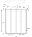
- FIG. 1 is a schematic plan view showing an organic EL light emitting device according to an embodiment of the present invention.
- FIG. 2 is an end view of the organic EL light emitting device of FIG. 1 cut along a line II-II.
- (A) And (b) is a schematic plan view which shows the correspondence of two adjacent organic EL elements.
- the schematic plan view which shows the organic electroluminescent light-emitting device which concerns on the 1st modification of this invention.
- FIG. 5 is an end view of the organic EL light emitting device of FIG. 4 cut along a VV line. The end view which shows the organic electroluminescent light-emitting device which concerns on the 2nd modification of this invention.
- FIG. 11 is an end view of the organic EL light emitting device of FIG. 10 cut along a XI-XI line.
- the schematic plan view which shows one Embodiment of the organic EL element used by this invention.
- the present invention will be described below with reference to the drawings. However, it should be noted that dimensions such as layer thickness and length in each figure are different from actual ones. Also, in this specification, there are cases where the first, second, etc. are added as prefixes of terms, but these prefixes are added only for distinguishing terms, and the order, superiority, inferiority, etc. It has no special meaning.
- the direction in which the organic EL elements are arranged in parallel is referred to as the A direction
- the direction substantially orthogonal to the A direction is referred to as the B direction.
- Organic EL device Before describing the configuration of the organic EL light-emitting device of the present invention, the basic configuration of the organic EL element used in the present invention will be described.
- the organic EL element used in the present invention has an element substrate and an organic EL layer laminated on the element substrate.
- the organic EL layer includes a first electrode layer stacked on the element substrate, an organic layer stacked on the first electrode layer, and a second electrode layer stacked on the organic layer.
- the layer structure of the organic EL element is not particularly limited as long as the above conditions are satisfied, and an arbitrary layer can be added.
- the organic EL element may be a top emission type element that can extract light from the front side of the element substrate (the side on which the organic EL layer is laminated), or may extract light from the back side of the element substrate. It may be a bottom emission type element that can be used.
- the organic EL element used in the present invention has electrode terminals (anode terminal and cathode terminal) capable of energizing the first and second electrode layers.
- the electrode terminal capable of energizing the first electrode layer is an anode terminal
- the electrode terminal capable of energizing the second electrode layer is a cathode. Terminal.
- the planar shape of the organic EL element is not particularly limited, but generally, an organic EL element having a substantially rectangular shape in plan view is used, and preferably, an organic EL element having a substantially strip shape in plan view is used. If an organic EL element having a substantially band shape in plan view is used, a large organic EL light-emitting device can be obtained by arranging a plurality of organic EL elements in parallel in the width direction.
- the size of the organic EL element having a substantially band shape in plan view is not particularly limited, but generally, the width: length of the organic EL element is 1: 3 to 1:20, preferably 1: 3 to 1: 10.
- the organic EL element 5 used in the present invention is preferably provided with electrode terminals (anode terminal 521 and cathode terminal 541) at both ends in the width direction.
- electrode terminals anode terminal 521 and cathode terminal 541 at both ends in the width direction.
- the left end in the width direction is the anode terminal 521
- the right end in the width direction is the cathode terminal 541.
- the first electrode layer 52 laminated on the element substrate 51 is an anode layer
- the second electrode layer 54 provided on the organic layer 53 is a cathode layer.
- the anode layer and the cathode layer may be reversed.
- FIGS. 1 and 2 a portion with a lattice pattern is a surface region 56 corresponding to the organic layer 53 of the organic EL element.
- FIGS. 9 to 11 The organic EL element 5 used in FIGS. 1 and 2, FIGS. 4 to 7, and FIGS. 9 to 11 is shown in FIGS. This is the organic EL element 5. 1 and 2, FIG. 4 to FIG. 7, and FIG. 9 to FIG. 11, the organic EL elements 5 in a planar view shown in FIG. 12 are arranged in parallel in the width direction. That is, in the illustrated example, the width direction of the organic EL element 5 corresponds to the A direction.
- the organic EL light emitting device of the present invention includes a light emitting panel having a base material and a plurality of organic EL elements arranged in parallel in the A direction on the base material.
- the organic EL element has an organic layer and electrode terminals (anode terminal and cathode terminal).
- the light emitting panel further includes a connection portion in which the electrode terminals of the respective organic EL elements are electrically connected.
- the electrode terminals (anode terminal and cathode terminal) of the organic EL element located at both ends of the light emitting panel are electrically connected to an external power source. Then, when a current is passed from the external power source to the electrode terminal, the light emitting layer included in the organic layer emits light.
- the organic EL light emitting device of the present invention includes a sealing member that includes a light emitting region composed of a plurality of organic layers and an interlayer region sandwiched between two adjacent organic layers in the light emitting panel.
- FIG. 1 is a schematic plan view showing an organic EL light emitting device 1 according to an embodiment of the present invention
- FIG. 2 is a schematic end view thereof.
- the connector member 61 provided in the space between the sealing member 3 and the light emitting panel 2 is represented by an alternate long and short dash line.
- the light-emitting panel 2 is formed of a base material 21 and a plurality of (for example, four) organic EL elements 5 arranged in parallel in the A direction in a tile shape on the base material 21.
- the plurality of organic EL elements 5 having a substantially band shape in plan view are regularly arranged in parallel with a slight gap in the width direction.
- the organic EL elements 5 arranged in parallel are fixed to the base material 21.
- the base material is preferably a flexible sheet.
- the base material is made of, for example, a material similar to a substrate of a connection substrate and an element substrate of an organic EL element described later.
- the base material may be either transparent or opaque, but in the case of forming a bottom emission type organic EL light emitting device, a transparent base material is used.
- the base material preferably has sealing properties (gas barrier property and water vapor barrier property).
- examples of the transparent index include a total light transmittance of 70% or more, preferably 80% or more.
- the total light transmittance refers to a value measured by a measuring method in accordance with JIS K7105 (plastic optical property test method).
- oxygen permeability is not more than 500cc / m 2 ⁇ day ⁇ atm , preferably not more than 100cc / m 2 ⁇ day ⁇ atm , more preferably, 50cc / m 2 ⁇ day ⁇ It can be exemplified that it is atm or less.
- the oxygen permeability is a value measured by a measuring method based on JIS K7126 in an atmosphere of 25 ° C.
- the water vapor permeability is 500 g / m 2 ⁇ day or less, preferably 100 g / m 2 ⁇ day or less, and more preferably 50 g / m 2 ⁇ day or less. Can be illustrated. However, the water vapor permeability is a value measured by a measurement method based on JIS K7129 in an atmosphere of 40 ° C. and 90% RH.
- the organic EL elements 5 in the light emitting panel 2 are arranged in parallel in the A direction so that the anode terminal 521 and the cathode terminal 541 are adjacent to each other.
- the anode terminal 521 and the cathode terminal 541 which are adjacent to each other as described above are electrically connected via the conductive connector member 61 straddling the electrode terminals 521 and 541. That is, in FIG. 1 and FIG. 2, the connection portion 6 includes the connector member 61.
- the anode terminal 521 of the organic EL element 5 located at one end of the light emitting panel 2 and the cathode terminal 541 of the organic EL element 5 located at the other end of the light emitting panel 2 are connected to an external power source (not shown). Lead wires 7 are connected to each other.
- the connecting portion 6 includes the connector member 61, but the present invention is not limited to this embodiment.
- position so that the side edge of the adjacent organic EL element 5 may contact
- the connector member 61 can be omitted.
- the contact points of the electrode terminals 521 and 541 become the connection portion 6.
- the adjacent organic EL element 5 in the light emission panel 2 is connected in series via the connector member 61.
- the organic EL elements 5 may be connected in parallel through conductive lead wires connected to the electrode terminals 521 and 541 of the organic EL elements 5 (not shown).
- the connection part 6 has a leader line.
- the side edge of the organic EL element 5 is a part which comprises the outline of the organic EL element 5 when it sees from the perpendicular direction with respect to the surface.
- a connector member will not be specifically limited if it has electroconductivity,
- the metal lump which has electroconductivity can be used.
- the lead wire forming material is not particularly limited as long as it has conductivity.
- a material obtained by processing a conductive metal into a linear shape can be used.
- the shape of a connector member or a lead wire is not specifically limited. 1 and 2, an elongated connector member 61 having substantially the same length as the organic EL element 5 is used.
- the light emitting panel 2 includes four organic EL elements 5, but the number of organic EL elements 5 constituting the light emitting panel 2 is not particularly limited.
- One light-emitting panel 2 is configured by using two or more organic EL elements 5, preferably by using 3 to 20 organic EL elements 5, and more preferably by 4 to 15 organic EL elements. It is configured using the element 5.
- Light emitting region and interlayer region By arranging a plurality of organic EL elements in a tile shape in parallel in the light emitting panel, a light emitting region composed of a plurality of organic layers and an interlayer region sandwiched between two adjacent organic layers are formed.
- the sealing member seals the light emitting region and the interlayer region.
- the light emitting region and the interlayer region will be described in detail.
- FIGS. 3A and 3B are schematic plan views showing an organic EL light emitting device having two organic EL elements.
- the base material, the connector member, the sealing member, and the like included in the organic EL light emitting device are omitted for convenience.
- the organic EL element is also shown shorter than usual.
- the interval between the organic EL elements is shown wider than usual for convenience.
- the two organic EL elements 5 each have a surface region 56 corresponding to the organic layer 53.
- the organic EL element 5 in the figure has surface regions 56 at the electrode terminals 521 and 541 and at portions excluding both ends in the longitudinal direction of the organic EL element 5 and the vicinity thereof.
- a lattice pattern is attached to the surface region 56.
- the light emitting region 22 is a region in which the surface regions 56 of all the organic EL elements 5 included in the organic EL light emitting device are combined.
- FIGS. 3A and 3B the region in which the two surface regions 56 and 56 are combined. It is.
- the light emitting panel 2 since the light emitting panel 2 includes four organic EL elements 5, the light emitting region 22 is formed by the four surface regions 56.
- the interlayer region 23 includes two side regions 561 and 561 of two surface regions 56 and 56 extending in the B direction, and side edges 562 of two surface regions 56 and 56 extending in the A direction. This is an area surrounded by two imaginary lines C and C connecting the ends of 562.
- the interlayer region 23 is represented by countless dots.
- the interlayer region 23 includes a cathode terminal 541 of the organic EL element 5 located on the left side in the drawing, an anode terminal 521 of the organic EL element 5 located on the right side, and both electrode terminals 521 and 541. And an area including the intervening area. Further, as shown in FIG.
- the interlayer region 23 is This is a region including the cathode terminal 541 of the organic EL element 5 arranged on the left side and the anode terminal 521 of the organic EL element 5 arranged on the right side.
- the sealing member is sealed so as to include a plurality of surface regions (light emitting regions) and interlayer regions.
- one sealing member is provided so as to straddle between a plurality of organic EL elements, and a plurality of surface regions (light emitting regions) and interlayer regions are sealed together by one sealing member.
- the connection part (connector member) is abbreviate
- the connection part (connector member) is sealed with the sealing member.
- the position where the connector member is provided is not particularly limited, but is preferably provided so that the connector member is located in the interlayer region 23.
- the sealing member 3 includes a side wall portion 31 that surrounds at least the light emitting region 22 and the interlayer region 23, and a ceiling portion 32 that covers the light emitting region 22 and the interlayer region 23. 1 and 2, the side wall 31 of the sealing member 3 is erected from the surface of the base material 21 via the adhesive layer 8. The side wall 31 of the sealing member 3 surrounds the plurality of organic EL elements 5. As described above, the connection portion 6 having the light emitting region 22, the interlayer region 23, and the connector member 61 is surrounded by the side wall portion 31 of the sealing member 3 and is covered by the ceiling portion 32 of the sealing member 3. . As shown in FIGS.
- the ceiling portion 32 of the sealing member 3 has a substantially rectangular shape in plan view, and the sealing member 3 has a substantially inverted U shape in cross-sectional view.
- the lead wire 7 electrically connected to the anode terminal 521 and the cathode terminal 541 of the organic EL element 5 located at both ends of the light emitting panel 2. Is partially sealed.
- the sealing member can prevent the outside air from entering the sealed space, it is possible to prevent the organic layer from being deteriorated by the outside air.
- members other than an organic EL element, a connector member, and a lead wire may be sealed in the sealing space. However, in the present specification, description of these members is omitted, and is not displayed on the drawings.
- the sealed space may be filled with an inert gas such as helium gas or nitrogen gas.
- a desiccant and / or an oxygen absorber may be disposed in the sealed space.
- the sealed space is filled with an inert gas, and a desiccant and an oxygen absorbent are disposed.
- the desiccant is not particularly limited, and a desiccant that chemically adsorbs moisture and maintains a solid state even when moisture is absorbed is used. Examples of such compounds include sodium oxide, potassium oxide, calcium oxide, and barium oxide.
- the oxygen absorbent is not particularly limited, and examples thereof include aluminum, iron, sodium, lithium, barium, and zinc.
- Filling the sealed space with an inert gas can more effectively prevent the organic layer from coming into contact with the outside air. Further, even when outside air enters the sealed space, if the desiccant and the oxygen absorbent are arranged in the sealed space, it is possible to effectively prevent the entered outside air from contacting the organic layer.
- the sealing member may be further laminated with a first barrier layer that prevents intrusion of outside air.
- the first barrier layer 34 is laminated on the ceiling portion 32 of the sealing member 3.
- the material for forming the first barrier layer is not particularly limited, and examples thereof include a metal vapor deposition film, a metal or silicon oxide film, an oxynitride film, a nitride film, and a metal foil.
- the metal of the metal deposition film include In, Sn, Pb, Cu, Ag, Ti, and the like.
- the metal oxide include MgO, SiO, Si x O y , Al 2 O 3 , GeO, and Ti 2 O.
- Examples of the metal foil include aluminum, copper, and stainless steel.
- the thickness of the first barrier layer is not particularly limited, but is, for example, 50 nm to 50 ⁇ m.
- the side wall portion of the sealing member is a portion surrounding at least the light emitting region and the interlayer region.
- the material for forming the side wall is not particularly limited as long as it has sealing properties.
- the side wall portion is formed from a resin having a sealing property. Examples of such resins include ethylene-vinyl alcohol copolymer, polyvinylidene chloride, nylon 6, nylon 66, polymetaxylylene adipamide, amorphous polyamide, polyethylene terephthalate, epoxy resin, and mixtures thereof.
- the thickness of the side wall portion is not particularly limited as long as the sealing property of the sealing member can be ensured.
- the thickness of the side wall is 0.3 mm to 3 mm, preferably 0.3 mm to 2 mm, and more preferably 0.3 mm to 1 mm. If the thickness of the side wall portion is less than 0.3 mm, the sealing performance of the sealing member may not be ensured, and if the thickness of the side wall portion exceeds 3 mm, the flexibility of the organic EL light emitting device may be impaired. .
- the ceiling part of the sealing member is a part that covers the light emitting region and the interlayer region.
- the material for forming the ceiling is not particularly limited as long as it has sealing properties.
- the ceiling part is formed of a transparent material.
- a transparent material By using a transparent material, it is possible to prevent light emitted from the top emission type organic EL element from being blocked by the ceiling. Examples of such a transparent material include glass and resin.
- the transparent resin the same resin as the material for forming the side wall portion can be used.
- the thickness of a ceiling part will not be specifically limited if it is a range which can ensure the sealing performance of a sealing member.
- the thickness of the ceiling is 0.05 mm to 3 mm, preferably 0.1 mm to 2 mm, and more preferably 0.1 mm to 1 mm.
- the method for manufacturing the sealing member is not particularly limited.
- the sealing member can be produced, for example, by forming a bottomless cylindrical side wall portion and then joining the ceiling portion so as to close one opening portion of the bottomless cylindrical shape.
- the ceiling part of a sealing member uses the same resin as the formation material of the said side wall part. If the forming material of the ceiling part and the side wall part is the same, a sealing member in which the side wall part and the ceiling part are seamlessly integrated can be obtained by injection molding or the like. Since the sealing member having no joint between the side wall portion and the ceiling portion does not cause separation of the ceiling portion and the side wall portion, it is possible to more effectively prevent intrusion of outside air.
- the connector member 61 may be provided in the one side part (upper part part in the figure) of the light emission panel 2. As shown in FIG. Since the connector member 61 is unevenly distributed on one side of the light-emitting panel 2 as described above, the material for forming the connector member 61 can be reduced, so that the lighter organic EL light-emitting device 1 can be obtained.
- the electrode terminals 521 and 541 located in the both ends of the light emission panel 2 may be exposed to the outer side of the sealing member 3.
- the side wall portion 31 of the sealing member 3 passes through the adhesive layer 8 from the surface of the electrode terminals (the anode terminal 521 and the cathode terminal 541) of the organic EL element 5 located at both ends of the light emitting panel 2.
- the organic layer 53 can be prevented from coming into contact with the outside air.
- the sealing member 3 may be a resin layer 35 that covers at least the light emitting region 22 and the interlayer region 23 without a gap.
- the sealing member 3 made of the resin layer 35 covers all the organic EL elements 5 in the light emitting panel 2 without any gap. That is, the connection portion 61 including the light emitting region 22, the interlayer region 23, and the connector member 61 in the light emitting panel 2 is sealed with the resin layer 35 that is the sealing member 3.
- the first barrier layer 34 described above may be laminated on the sealing member 3 (resin layer 35) (not shown). In FIG. 6, for convenience, the end surface of the resin layer 35 is not hatched, and countless dots are appended instead.
- the sealing member made of the resin layer is less likely to cause peeling of the sealing member at the boundary between the base material and the sealing member, and is difficult for outside air to enter. Therefore, deterioration of the organic layer can be effectively prevented.
- Resin used for a resin layer is not specifically limited, The same resin as what is used for said side wall part can be used.
- the resin used for the resin layer is preferably transparent.
- the resin layer 35 is provided so as to cover the entire surface of the electrode terminals located at both ends of the light emitting panel 2. However, the resin layer 35 may cover only a part of the electrode terminals located at both ends of the light emitting panel 2, and a part of the electrode terminals may be exposed outside the resin layer 35 (not shown).
- the material for forming the resin layer 35 is not particularly limited as long as it is a resin having a sealing property.
- the resins listed as the material for forming the side wall portion can be used.
- the shortest distance X between the side edge surface 351 of the resin layer 35 and the organic layer 53 is preferably 0.5 mm to 4 mm, more preferably 2 mm to 4 mm.
- the shortest distance Y between the surface 352 of the resin layer 35 and the surface of the organic layer 53 is preferably 0.05 mm to 3 mm, more preferably 0.1 mm to 3 mm.
- the sealing member 3 may be a flexible film 36 having flexibility and sealing properties as shown in FIG.
- the flexible film 36 is laminated so as to straddle the surfaces of the plurality of organic EL elements 5 included in the light emitting panel 2.
- the peripheral portion of the flexible film 36 shown in FIG. 7 is bonded onto the base material 21 via the adhesive layer 8.
- the thickness of the flexible film 36 is not particularly limited as long as the sealing property can be ensured, and is, for example, 0.05 mm to 3 mm, preferably 0.1 mm to 2 mm, more preferably 0.1 mm to 1 mm.
- the forming material of the flexible film 36 is not particularly limited as long as it is a resin having sealing properties, and for example, the resins listed as the forming material of the side wall portion can be used. Further, the flexible film 36 may have a single layer structure or a multilayer structure having two or more layers.
- the organic EL light emitting device of the present invention may have a connection substrate having a connector member and a substrate on which the connector member is disposed.
- Each organic EL element is electrically connected by connecting a connection board
- FIG. 8 is a schematic rear view showing an embodiment of the connection substrate 4 used in the present invention
- FIG. 9 is a state in which the connection substrate 4 and the plurality of organic EL elements 5 (light emitting panel 2) are electrically connected.
- FIG. 10 is a schematic plan view showing the organic EL light-emitting device 1 of the present invention obtained by providing the sealing member 3 on the connection substrate 4 and the plurality of organic EL elements 5 of FIG.
- the first and second connection circuits 411 and 412 of the connection substrate 4 are provided with countless dots
- the connector member 61 that is the connection portion 6 is provided with a lattice pattern. ing.
- FIG. 8 is a schematic rear view showing an embodiment of the connection substrate 4 used in the present invention
- FIG. 9 is a state in which the connection substrate 4 and the plurality of organic EL elements 5 (light emitting panel 2) are electrically connected.
- FIG. 10 is a schematic plan view showing the organic EL light-emitting device 1 of the present invention obtained by providing the sealing
- connection substrate 4 the first and second connection circuits 411 and 412 and the connector member 61 of the connection substrate 4 are indicated by a one-dot chain line for convenience.
- FIG. 11 for convenience, the end surface of the resin layer 35 is not hatched, and countless dots are appended instead.
- connection board 4 includes a connection circuit 41, a connector member 61, and a board 42 provided with the connection circuit 41 and the connector member 61.
- the connection circuit 41 is a member that connects the organic EL element 5 in the light emitting panel 2 to the external power source 9.
- the connector member 61 is a member that electrically connects the electrode terminals (the anode terminal 521 and the cathode terminal 541) of two adjacent organic EL elements 5 in the light emitting panel 2.
- the connection circuit 41 includes a first connection circuit 411 connected to the anode terminal 521 of the organic EL element 5 and a second connection circuit 412 connected to the cathode terminal 541 of the organic EL element 5.
- One end of both connection circuits 411 and 412 is connected to the anode terminal 521 or the cathode terminal 541 of the organic EL element 5, and the other end of both connection circuits 411 and 412 is connected to the external power supply 9.
- the connector member 61 is a member formed so as to straddle the anode terminal 521 and the cathode terminal 541 of the two adjacent organic EL elements 5 as described above.
- the adjacent organic EL elements 5 in the light emitting panel 2 are electrically connected via the connector member 61.
- substrate 42 is not specifically limited, For example, as shown in FIG. 8, it is set as the substantially rectangular shape from which one side protruded partially.
- the other end portion of the first connection circuit 411 and the other end portion of the second connection circuit 412 are disposed on the protruding portion.
- one end of the first connection circuit 411 and one end of the second connection circuit 412 are disposed at the end of the substrate 42 facing the protruding portion in the plane of the substrate 42.
- three connector members 61 are provided intermittently between the one end portion of the first connection circuit 411 and the one end portion of the second connection circuit 412 with a required interval.
- connection board may have portions other than the first and second connection circuits and the connector member. However, in the present specification, description of these portions is omitted and is not displayed on the drawings.
- connection circuit and the connector member on the substrate is not particularly limited.
- the connection circuit and the connector member are preferably formed by the same method, but may be formed by different methods.
- the connection circuit may be formed by printed wiring
- the connector member may be formed by soldering.
- each organic EL element 5 in the light emitting panel 2 includes an anode terminal 521 and a cathode terminal except for electrode terminals (anode terminal 521 and cathode terminal 541) located at both ends of the light emitting panel 2.
- 541 are arranged in parallel in the A direction so as to be adjacent to each other.
- the adjacent anode terminal 521 and cathode terminal 541 are electrically connected via the connector member 61 of the connection board 4.
- the anode terminal 521 and the cathode terminal 541 located at both ends of the light emitting panel 2 are connected to the first connection circuit 411 and the second connection circuit 412 of the connection substrate 4.
- the part where the electrode terminals 411 and 412 of two adjacent organic EL elements 5 in the light emitting panel 2 are connected is sealed with a sealing member.
- connection substrate 4 is connected so as to cover one side of the light emitting panel 2. That is, the connection substrate 4 is connected to the anode terminal 521 and the cathode terminal 541 of the plurality of organic EL elements 5 in the light emitting panel 2, whereby each organic EL element 5 is electrically connected and a plurality of organic EL elements are connected.
- the EL element 5 is integrated.
- the resin layer 35 as the sealing member 3 covers the plurality of organic EL elements 5 in the light emitting panel 2 and the connection substrate 4 connected to the plurality of organic EL elements 5 without any gap.
- connection portion 6 including the light emitting region 22, the interlayer region 23, and the connector member 61 in the light emitting panel 2 is embedded by the resin layer 35 that is the sealing member 3. Therefore, the sealing member 3 (resin layer 35) can not only prevent the organic layer 53 from coming into contact with the outside air but also firmly fix the connection between the plurality of organic EL elements 5 and the connection substrate 4. Since the connection between the plurality of organic EL elements 5 and the connection substrate 4 is firmly fixed, the connection substrate 4 can be prevented from falling off.
- the shortest distance X between the side edge surface 351 of the resin layer 35 and the organic layer 53 is preferably 0.5 mm to 4 mm, and more preferably 2 mm to 4 mm.
- the shortest distance Z between the surface 352 of the resin layer 35 and the surface of the organic layer 53 is preferably 0.05 mm to 5 mm, more preferably 0.1 mm to 5 mm.
- connection substrate is a member that electrically connects a plurality of organic EL elements in the light emitting panel, supplies current from an external power source to the light emitting panel, and integrates the plurality of organic EL elements in the light emitting panel.
- One connection board is attached to one light emitting panel.
- the connection substrate is a member that integrates a plurality of organic EL elements in the light-emitting panel.
- substrate which is a structural member of a connection board
- polyester resins such as polyethylene terephthalate (PET), polyethylene naphthalate (PEN), polybutylene terephthalate (PBT); polyethylene (PE), polypropylene (PP), polymethylpentene (PMP), Olefin resins containing ⁇ -olefin as a monomer component such as ethylene-propylene copolymer and ethylene-vinyl acetate copolymer (EVA); polyvinyl chloride (PVC); vinyl acetate resin; polycarbonate (PC); polyphenylene sulfide (PPS); amide resins such as polyamide (nylon) and wholly aromatic polyamide (aramid); polyimide resins; polyether ether ketone (PEEK), and the like, preferably polyimide resins.
- the thickness of the substrate is not particularly limited, but is preferably 10 ⁇ m to 50 ⁇ m, more preferably 10 ⁇ m to 30 ⁇ m.
- an insulating substrate is used so that the connection circuit and the connector member are not electrically connected.
- the resin film forming materials listed above usually have insulating properties.
- an insulating layer is provided at least in a region where the connection circuit and the connector member are provided on the surface of the substrate.
- the substrate may be transparent or opaque.
- a transparent substrate is used. By using a transparent substrate, it is possible to prevent light emitted from the top emission type organic EL element from being blocked by the connection substrate.
- the size of the substrate is not particularly limited and can be designed as appropriate.
- substrate is not specifically limited, According to the arrangement
- connection circuit is a part that supplies current from an external power source to the light-emitting panel.
- the connection circuit includes a first connection circuit that is electrically connected to the anode terminal of the organic EL element, and a second connection circuit that is electrically connected to the cathode terminal.
- One end portions of the first and second connection circuits are connected to an anode terminal and a cathode terminal, respectively, and the other end portions thereof are connected to an anode and a cathode of an external power source.
- the other end portions of the first and second connection circuits may be directly connected to the external power supply, but may be indirectly connected to the external power supply via other members such as an IC chip.
- connection circuit is made of a conductive material, and its shape is not particularly limited.
- the connection circuit is preferably composed of wiring formed in a linear shape on the substrate, and more preferably is composed of printed wiring formed by attaching a thin film of a conductive material on the substrate.
- the material for forming the connection circuit is not particularly limited, and examples thereof include conductive materials such as metals such as platinum, gold, silver, copper, nickel, cobalt, and titanium; metal oxides such as ITO; inorganic materials such as graphite; . Since the electrical resistance is low, the forming material of the connection portion is preferably copper.
- a connector member is a part electrically connected so that the anode terminal and cathode terminal of an adjacent organic EL element in a light emission panel may be straddled.
- the shape of the connector member in plan view is not particularly limited, but is preferably elongated in plan view. If the connection substrate and the plurality of organic EL elements (light emitting panels) are connected, the adjacent anode terminal and cathode terminal can be connected even if there is a slight misalignment.
- the connector member is made of a conductive material.
- the connector member may be formed from, for example, wiring such as the above-described printed wiring, or may be formed from a lump of conductive material fixed on the substrate. Examples of the material for forming the connector portion include the material for forming the connection circuit.
- a connection substrate in which a connection circuit and a connector member are printed on a flexible substrate is particularly preferably used.
- a connection substrate printed and wired on a flexible substrate is generally called a flexible printed circuit board (FPC). Since the wiring pattern can be easily changed by using the FPC, the arrangement of the connector member and the connection circuit can be easily set. Therefore, a connection board suitable for the arrangement of the organic EL elements in the light emitting panel can be easily and inexpensively formed.
- FPC flexible printed circuit board
- the organic EL element used in the organic EL light emitting device of the present invention is not particularly limited as long as it has an organic layer, an anode terminal, and a cathode terminal. However, preferably, as described above, the organic EL elements shown in FIGS. 12 and 13 are used. Hereinafter, the layer structure of the organic EL element will be described.
- the element substrate is not particularly limited, and examples thereof include a glass substrate, a metal substrate, a synthetic resin substrate, and a ceramic substrate.
- the synthetic resin substrate include polyester resins such as polyethylene terephthalate (PET), polyethylene naphthalate (PEN), and polybutylene terephthalate (PBT); polyethylene (PE), polypropylene (PP), polymethylpentene (PMP), and ethylene.
- -Olefin resins containing ⁇ -olefin as monomer component such as propylene copolymer, ethylene-vinyl acetate copolymer (EVA); polyvinyl chloride (PVC); vinyl acetate resin; polycarbonate (PC); PPS); Amide resins such as polyamide (nylon), wholly aromatic polyamide (aramid); polyimide resins; flexible synthetic resin films such as polyetheretherketone (PEEK).
- the metal substrate include a flexible thin plate made of stainless steel, copper, titanium, aluminum, an alloy, or the like.
- the element substrate is preferably excellent in heat dissipation.
- the element substrate preferably has a sealing property. Note that in the case of using a metal substrate, an insulating layer is provided on the surface of the metal substrate in order to insulate the electrode formed on the surface.
- the anode layer is made of a conductive film.
- the material for forming the anode layer is not particularly limited.
- ITO indium tin oxide
- ITSO indium tin oxide containing silicon oxide
- the thickness of the anode layer is not particularly limited, but is usually 0.01 ⁇ m to 1.0 ⁇ m.
- an optimum method can be adopted depending on the forming material, and examples thereof include a sputtering method, a vapor deposition method, and an ink jet method. For example, when forming an anode with a metal, a vapor deposition method is used.
- the anode layer 52 of the organic EL element 5 shown in FIG. 12 and FIG. 13 has an anode terminal 521 whose one end (left end in the drawing) is exposed.
- the anode terminal 521 only needs to be able to pass a current from an external power source to the anode layer 52 and may not be a portion where the anode layer 52 is exposed.
- the anode terminal 521 may be formed by laminating an auxiliary electrode layer on the exposed surface of the anode layer 52 (not shown). By passing the auxiliary electrode layer, it is possible to apply a voltage uniformly to the entire organic EL layer.
- the organic layer is a laminate composed of at least two functional layers.
- the structure of the organic layer for example, (A) a structure composed of three layers, a hole transport layer, a light emitting layer, and an electron transport layer, and (B) composed of two layers, a hole transport layer and a light emitting layer. Examples thereof include a structure, (C) a structure composed of two layers of a light emitting layer and an electron transport layer.
- the organic layer (B) the light emitting layer also serves as the electron transport layer.
- the organic layer (C) the light emitting layer also serves as the hole transport layer.
- the organic layer of the organic EL device used in the present invention may have any of the structures (A) to (C).
- the organic EL element of FIG. 11 has the structure (A).
- the organic layer having the structure (A) will be described.
- the hole transport layer 531 included in the organic layer 53 has a function of injecting holes into the light emitting layer 532
- the electron transport layer 533 has a function of injecting electrons into the light emitting layer 532.
- the organic EL element 5 electrons and holes injected from the anode layer 52 and the cathode layer 54 to the light emitting layer 532 are recombined to generate excitons. When the exciton returns to the ground state, the light emitting layer emits light.
- the hole transport layer is provided on the surface of the anode layer.
- any functional layer other than these may be interposed between the anode layer and the hole transport layer on condition that the luminous efficiency of the organic EL element is not lowered.
- the hole injection layer may be provided on the surface of the anode layer, and the hole transport layer may be provided on the surface of the hole injection layer.
- the hole injection layer is a layer having a function of assisting injection of holes from the anode layer to the hole transport layer. By providing the hole injection layer, holes are easily injected from the hole transport layer into the light emitting layer.
- the hole transport layer substantially has the function of a hole injection layer even if no hole injection layer is provided.
- a hole transport layer can also be formed.
- the material for forming the hole transport layer is not particularly limited as long as it is a material having a hole transport function.
- aromatic amine compounds such as 4,4 ′, 4 ′′ -tris (carbazol-9-yl) -triphenylamine (abbreviation: TcTa); 1,3-bis (N— Carbazole derivatives such as carbazolyl) benzene; spiros such as N, N′-bis (naphthalen-1-yl) -N, N′-bis (phenyl) -9,9′-spirobisfluorene (abbreviation: Spiro-NPB)
- Spiro-NPB 1,3-bis (N— Carbazole derivatives such as carbazolyl) benzene
- Spiro-NPB 1,3-bis (N— Carbazole derivatives such as carbazolyl) benzene
- Spiro-NPB 1,3-bis (N— Carbazole derivatives such as carbazolyl)
- the material for forming the hole injection layer is not particularly limited, and examples thereof include metal oxides such as vanadium oxide, niobium oxide, and tantalum oxide; phthalocyanine compounds such as phthalocyanine; hexaazatriphenylene hexacarbonitrile (abbreviation: HAT- CN) and the like; polymer compounds such as a mixture of 3,4-ethylenedioxythiophene and polystyrenesulfonic acid (abbreviation: PEDOT / PSS); and the like.
- the material for forming the hole injection layer may be used alone or in combination of two or more.
- the hole injection layer may have a multilayer structure of two or more layers.
- the thicknesses of the hole transport layer and the hole injection layer are not particularly limited, but are preferably 1 nm to 500 nm from the viewpoint of lowering the driving voltage.
- a method for forming the hole transport layer and the hole injection layer an optimum method can be adopted depending on the forming material, and examples thereof include a sputtering method, a vapor deposition method, an inkjet method, and a coating method.
- the light emitting layer is provided on the surface of the hole transport layer.
- the material for forming the light emitting layer is not particularly limited as long as it is a light emitting material.
- a material for forming the light emitting layer for example, a low molecular light emitting material such as a low molecular fluorescent light emitting material or a low molecular phosphorescent light emitting material can be used.
- low-molecular light-emitting material examples include aromatic dimethylidene compounds such as 4,4′-bis (2,2′-diphenylvinyl) -biphenyl (abbreviation: DPVBi); 5-methyl-2- [2- [4- Oxadiazole compounds such as (5-methyl-2-benzoxazolyl) phenyl] vinyl] benzoxazole; 3- (4-biphenylyl) -4-phenyl-5-tert-butylphenyl-1,2,4 A triazole derivative such as triazole; a styrylbenzene compound such as 1,4-bis (2-methylstyryl) benzene; a benzoquinone derivative; a naphthoquinone derivative; an anthraquinone derivative; a fluorenone derivative; an azomethine zinc complex, tris (8-quinolinolato) aluminum (Alq) 3 ) organometallic complexes such as;
- a host material doped with a light emitting dopant material may be used as a material for forming the light emitting layer.
- the host material for example, the above-described low-molecular light-emitting materials can be used, and in addition, 1,3,5-tris (carbazo-9-yl) benzene (abbreviation: TCP), 1,3-bis (N-carbazolyl) benzene (abbreviation: mCP), 2,6-bis (N-carbazolyl) pyridine, 9,9-di (4-dicarbazole-benzyl) fluorene (abbreviation: CPF), 4,4′-bis A carbazole derivative such as (carbazol-9-yl) -9,9-dimethyl-fluorene (abbreviation: DMFL-CBP) can be used.
- TCP 1,3,5-tris
- mCP 1,3-bis (N-carbazolyl) benzene
- CPF 9,9
- Examples of the dopant material include styryl derivatives; perylene derivatives; tris (2-phenylpyridyl) iridium (III) (Ir (ppy) 3 ), tris (1-phenylisoquinoline) iridium (III) (Ir (piq) 3 ), Phosphorescent metal complexes such as organic iridium complexes such as bis (1-phenylisoquinoline) (acetylacetonato) iridium (III) (abbreviation: Ir (piq) 2 (acac)), and the like.
- the material for forming the light emitting layer may include the above-described material for forming the hole transport layer, the material for forming the electron transport layer described later, and various additives.
- the thickness of the light emitting layer is not particularly limited, but is preferably 2 nm to 500 nm, for example.
- a method for forming the light emitting layer an optimum method can be adopted depending on the forming material, but it is usually formed by vapor deposition.
- the electron transport layer is provided on the surface of the light emitting layer (the back surface of the cathode layer).
- any functional layer other than these may be interposed between the cathode layer and the electron transport layer on condition that the luminous efficiency of the organic EL element is not lowered.
- the electron injection layer may be provided on the surface of the electron transport layer, and the cathode layer may be provided on the surface of the electron injection layer.
- the electron injection layer is a layer having a function of assisting injection of electrons from the cathode layer to the electron transport layer.
- an electron injection layer By providing the electron injection layer, electrons are easily injected from the electron transport layer into the light emitting layer.
- a material having both an electron transport function and an electron injection function as a material for forming an electron transport layer, a hole transport layer substantially having the function of an electron injection layer can be formed without providing an electron injection layer. You can also
- the material for forming the electron transport layer is not particularly limited as long as the material has an electron transport function.
- Examples of the material for forming the electron transport layer include tris (8-quinolinolato) aluminum (abbreviation: Alq 3 ), bis (2-methyl-8-quinolinolato) (4-phenylphenolato) aluminum (abbreviation: BAlq), and the like.
- the material for forming the electron injection layer is not particularly limited, and examples thereof include alkali metal compounds such as lithium fluoride (LiF) and cesium fluoride (CsF); alkaline earth metal compounds such as calcium fluoride (CaF 2 ); And a material for forming an electron transport layer.
- the material for forming the electron injection layer may be used alone or in combination of two or more.
- the electron injection layer may have a multilayer structure of two or more layers.
- the thicknesses of the electron transport layer and the electron injection layer are not particularly limited, but are preferably 1 nm to 500 nm from the viewpoint of lowering the driving voltage.
- an optimum method can be adopted depending on the material of formation, and examples thereof include a sputtering method, a vapor deposition method, an ink jet method, and a coating method.
- the cathode layer is made of a conductive film. Arbitrary functional layers other than these may be interposed between the cathode layer and the electron transport layer on condition that the luminous efficiency of the organic EL element is not lowered.
- the material for forming the cathode layer is not particularly limited. In the case of forming a top emission type organic EL element, a transparent cathode layer is used. As a material for forming a transparent and conductive cathode layer, indium tin oxide (ITO); indium tin oxide containing silicon oxide (ITSO); zinc oxide to which a conductive metal such as aluminum is added (ZnO: Al) A magnesium-silver alloy.
- the thickness of the cathode layer is not particularly limited, but is usually 0.01 ⁇ m to 1.0 ⁇ m.
- a method for forming the cathode layer an optimum method can be adopted depending on the forming material, and examples thereof include a sputtering method, a vapor deposition method, and an ink jet method.
- a sputtering method is used, and when the cathode layer is formed of a magnesium-silver alloy or a magnesium-silver laminated film, an evaporation method is used.
- the cathode layer 54 has a cathode terminal 541 whose one end (right end in the drawing) is exposed.
- the cathode terminal 541 only needs to be able to pass a current from the outside to the cathode layer 54 and is not a portion where the cathode layer 54 is exposed.
- the cathode terminal 541 can be formed by laminating an auxiliary electrode layer on the exposed surface of the cathode layer 54 (not shown).
- the second barrier layer is a layer that prevents the outside air from coming into contact with the organic layer 53.
- the second barrier layer 55 is stacked on the cathode layer 54.
- the material for forming the second barrier layer is not particularly limited, and the same material as that for the first barrier layer described above can be used.
- the thickness of the second barrier layer is not particularly limited, but is, for example, 50 nm to 50 ⁇ m.
- the organic EL light-emitting device manufacturing method of the present invention includes a step of arranging a plurality of organic EL elements each having an organic layer and an electrode terminal in a tile shape on a base material, and electrically connecting the electrode terminals of each organic electroluminescence element. And a light emitting panel forming step having a connecting step of forming a connection portion by connecting them together. Furthermore, the organic EL device manufacturing method of the present invention includes a light-emitting region composed of a plurality of organic layers in a light-emitting panel, and an sealing region sealed with a sealing member including an interlayer region sandwiched between two adjacent organic layers. It has a stop process.
- the light emitting panel formation process includes an arrangement process and a connection process.
- the arranging step is a step of arranging the plurality of organic EL elements described above in parallel on the base material in a tile shape.
- “arranging a plurality of organic EL elements in parallel in a tile shape” means that the organic EL elements are arranged so as not to overlap each other.
- the organic EL elements may be arranged so as to contact each other, or may be arranged at a necessary interval.
- the intervals may all be constant or may be different from each other.
- the interval between the organic EL elements is not particularly limited, but is usually 0.1 mm to 0.5 mm, and preferably 0.1 mm to 0.3 mm.
- a connection process is a process of forming a connection part by electrically connecting the electrode terminal of each organic electroluminescent element.
- the connecting portion is formed by the contact between the anode terminal of one adjacent organic EL element and the cathode terminal of the other organic EL element.
- the connection portion has a connector member.
- an independent connector member may be used, or a connection board having a connector member as used in Modification 3 of the present invention may be used.
- the connecting step includes a step of connecting the anode terminal and the cathode terminal of the organic EL element located at both ends of the light emitting panel to an external power source.
- an independent connector member an independent lead wire is connected to the electrode terminal of the organic EL element.
- a connection board having a connector member and a connection circuit as used in Modification 3 of the present invention it is not necessary to connect an independent lead wire to the electrode terminal of the organic EL element.
- connection method between these members and the electrode terminals is not particularly limited.
- connection method for example, wire bonding or solder reflow can be employed.
- substrate and an electrode terminal is not specifically limited.
- connection method for example, soldering or connection using an anisotropic conductive film (ACF) can be employed.
- the connection substrate is connected to a plurality of organic EL elements (light emitting panels) using ACF.
- the sealing step is a step of sealing using the above-described sealing member to include a light emitting region composed of a plurality of organic layers in the light emitting panel and an interlayer region sandwiched between two adjacent organic layers.
- a sealing member is a sealing member which has a side wall part and a ceiling part
- a sealing member consists of a resin layer
- a sealing member is a flexible film
- the sealing member is a sealing member having a side wall portion and a ceiling portion
- the organic layer is sealed by covering the light emitting panel with a sealing member prepared in advance.
- an adhesive is applied to the end of the side wall portion of the sealing member, the sealing member is bonded to the base material or the electrode terminal of the organic EL element, and then the adhesive is solidified to seal the sealing member.
- the members are bonded.
- the sealing member When the sealing member is bonded onto the base material and independent lead wires are connected to the electrode terminals located at both ends of the light emitting panel, the sealing member partially includes the lead wire and the base material. Glued on top. That is, a part of the lead wire is sealed in the sealing space and the other part is exposed outside the sealing space by the sealing process.
- a sealing process is preferably performed in inert gas atmosphere.
- the inert gas can be filled in the sealing space in parallel with the sealing step.
- the sealing member is a resin layer
- the light emitting region and the interlayer region are sealed by applying the molten resin on the base material and then solidifying the applied molten resin.
- coating molten resin on a base material the some organic EL element in a light emission panel is coat
- the sealing member partially embeds the lead wires. That is, in the sealing process, a part of the lead wire is embedded in the resin layer, and the other part is exposed to the outside of the resin layer.
- the sealing member is a flexible film
- an adhesive is applied to one surface of the flexible film, and then the flexible film is placed on the base material so as to cover a plurality of organic EL elements in the light-emitting panel.
- the light emitting region and the interlayer region are sealed by bonding together.
- sealing is performed including the connection portion formed in the connection step. That is, when the connector member is used in the connection process, the connection portion having the connector member is sealed in the sealing process.
- the connection substrate is used in the connection step, the connection between the connection substrate and the light-emitting panel can be further strengthened by sealing the connection portion having the connector member.
- the manufacturing method of the organic EL light emitting device of the present invention may further include a step of laminating the first barrier layer on the sealing member after the sealing step. By providing the first barrier layer, the organic layer is less likely to come into contact with the outside air.
- organic EL light emitting device and the manufacturing method thereof according to the present invention are not limited to the embodiment as described above, and can be appropriately changed in design within the range intended by the present invention.
- Example 1 Preparation of element substrate having insulating layer
- Acrylic resin manufactured by JSR Corporation, trade name “JEM-477”
- SUS304 stainless steel plate
- An anode layer made of an aluminum film having a thickness of 100 nm and HAT-CN having a thickness of 10 nm (1,4,5,8,9,12-hexaazatriphenylenehexacarbonitrile) on the insulating layer of the element substrate by vacuum deposition.
- a light emitting layer also serving as an electron transport layer
- Alq tris (8-quinolinolato) aluminum
- a cathode layer and a refractive index adjustment layer made of molybdenum trioxide having a thickness of 60 nm were deposited in this order.
- an organic EL layer was formed on the insulating layer of the element substrate to produce an organic EL element.
- a SiN film having a thickness of 200 nm was laminated by a sputtering method so as to cover a region (surface region) corresponding to the organic layer on the refractive index adjustment layer. Furthermore, an adhesive layer was formed by laminating an adhesive mainly composed of a low water content epoxy so as to have a thickness of 20 ⁇ m in the same region. Then, a PET film (trade name “DIAFOIL”, manufactured by Mitsubishi Plastics, Inc.) on which SiN was laminated to 200 nm was vacuum-laminated on the SiN film under the condition of being heated to 80 ° C. Thereafter, the adhesive layer was cured by heating at 100 ° C. for 2 hours.
- DIAFOIL manufactured by Mitsubishi Plastics, Inc.
- the SiN laminated PET film was bonded to the SiN film via the adhesive layer.
- the water vapor permeability of the adhesive layer was 40 g / m 2 ⁇ day.
- the 3rd 2nd barrier layer which consists of an adhesive bond layer, a SiN film
- connection substrate was a polyimide film having flexibility. That is, the connection board was FPC.
- the same SiN laminated PET film as used in the formation of the second barrier layer so as to cover the entire four organic EL elements arranged in parallel on the SUS base material (trade name “DIAFOIL” manufactured by Mitsubishi Plastics, Inc.) was laminated on the SUS base material.
- the same adhesive mainly composed of a low water content epoxy used in the formation of the second barrier layer was used. That is, the SiN laminated PET film was vacuum laminated on the entire organic EL element under the condition of being heated to 80 ° C. Thereafter, the adhesive layer was cured by heating at 100 ° C. for 2 hours. The thickness of the adhesive layer was 20 ⁇ m.
- a sealing member having a two-layer structure including a PET film on which SiN was laminated and an adhesive layer made of a low water content epoxy was bonded to the entire four organic EL elements.
- the total thickness of the sealing member was 70.2 ⁇ m.
- the sealing member was bonded together so that the connection part of a connection board
- the organic EL light emitting device according to Example 1 was manufactured by attaching the sealing member to the light emitting panel.
- Example 2 Instead of a PET film laminated with SiN, an EVA film having a thickness of 400 ⁇ m was vacuum-laminated under a condition heated to 100 ° C. as a sealing member, and between the EVA film and the four organic EL elements.
- An organic EL light emitting device according to Example 2 was produced in the same manner as in Example 1 except that the adhesive layer was not provided. That is, in Example 2, a sealing member made of only an EVA film was bonded to the entire four organic EL elements.
- the water vapor permeability of the EVA film was 18 g / m 2 ⁇ day.
- the total thickness of the sealing member was 400 ⁇ m.
- Example 3 Implemented except that a 700 ⁇ m thick glass plate was used as the base material instead of the stainless steel plate, and a 700 ⁇ m thick glass plate was used as the sealing member instead of the PET film laminated with SiN.
- An organic EL light emitting device according to Example 3 was produced by the same method as in Example 1.
- Comparative Example 1 An organic EL light emitting device according to Comparative Example 1 was produced in the same manner as in Example 1 except that sealing with a sealing member (PET film on which SiN was laminated) was not performed.
- the organic EL light-emitting device of the present invention can be used as a display device or a lighting device.
Landscapes
- Physics & Mathematics (AREA)
- Optics & Photonics (AREA)
- Engineering & Computer Science (AREA)
- Microelectronics & Electronic Packaging (AREA)
- Manufacturing & Machinery (AREA)
- Electroluminescent Light Sources (AREA)
Priority Applications (4)
| Application Number | Priority Date | Filing Date | Title |
|---|---|---|---|
| CN201380056930.2A CN104782228A (zh) | 2012-10-29 | 2013-10-01 | 有机电致发光装置和其制造方法 |
| US14/439,087 US20150303402A1 (en) | 2012-10-29 | 2013-10-01 | Organic electroluminescence device and method for manufacturing the same |
| KR1020157006827A KR20150079562A (ko) | 2012-10-29 | 2013-10-01 | 유기 일렉트로루미네센스 발광 장치, 및 그 제조 방법 |
| EP13851899.8A EP2914063A4 (de) | 2012-10-29 | 2013-10-01 | Organische elektrolumineszente lichtemittierende vorrichtung und verfahren zur herstellung davon |
Applications Claiming Priority (2)
| Application Number | Priority Date | Filing Date | Title |
|---|---|---|---|
| JP2012237857A JP2014089825A (ja) | 2012-10-29 | 2012-10-29 | 有機エレクトロルミネッセンス発光装置、及びその製造方法 |
| JP2012-237857 | 2012-10-29 |
Publications (1)
| Publication Number | Publication Date |
|---|---|
| WO2014069144A1 true WO2014069144A1 (ja) | 2014-05-08 |
Family
ID=50627060
Family Applications (1)
| Application Number | Title | Priority Date | Filing Date |
|---|---|---|---|
| PCT/JP2013/076690 WO2014069144A1 (ja) | 2012-10-29 | 2013-10-01 | 有機エレクトロルミネッセンス発光装置、及びその製造方法 |
Country Status (7)
| Country | Link |
|---|---|
| US (1) | US20150303402A1 (de) |
| EP (1) | EP2914063A4 (de) |
| JP (1) | JP2014089825A (de) |
| KR (1) | KR20150079562A (de) |
| CN (1) | CN104782228A (de) |
| TW (1) | TW201421672A (de) |
| WO (1) | WO2014069144A1 (de) |
Cited By (2)
| Publication number | Priority date | Publication date | Assignee | Title |
|---|---|---|---|---|
| JP2015228314A (ja) * | 2014-05-30 | 2015-12-17 | パナソニックIpマネジメント株式会社 | 電子デバイス及びその製造方法 |
| EP3076755A4 (de) * | 2013-11-28 | 2017-07-19 | Pioneer Corporation | Lichtemittierende vorrichtung |
Families Citing this family (10)
| Publication number | Priority date | Publication date | Assignee | Title |
|---|---|---|---|---|
| DE102013111732A1 (de) * | 2013-10-24 | 2015-04-30 | Osram Oled Gmbh | Optoelektronisches Bauelement, optoelektronische Baugruppe, Verfahren zum Herstellen eines optoelektronischen Bauelements und Verfahren zum Herstellen einer optoelektronischen Baugruppe |
| CN104269497B (zh) * | 2014-09-03 | 2017-01-18 | 深圳市华星光电技术有限公司 | 一种有机发光二极管封装结构及显示装置 |
| US9991326B2 (en) * | 2015-01-14 | 2018-06-05 | Panasonic Intellectual Property Management Co., Ltd. | Light-emitting device comprising flexible substrate and light-emitting element |
| KR102361711B1 (ko) * | 2015-02-02 | 2022-02-11 | 삼성디스플레이 주식회사 | 유기 발광 표시 장치 및 그 제조 방법 |
| WO2017038495A1 (ja) * | 2015-09-02 | 2017-03-09 | コニカミノルタ株式会社 | 照明装置および照明装置の製造方法 |
| US20170309852A1 (en) * | 2016-04-22 | 2017-10-26 | Semiconductor Energy Laboratory Co., Ltd. | Light-Emitting Element, Display Device, Electronic Device, and Lighting Device |
| KR102650330B1 (ko) * | 2016-08-24 | 2024-03-21 | 엘지디스플레이 주식회사 | 유기 발광 표시 장치 |
| CN108428804A (zh) * | 2018-04-19 | 2018-08-21 | 武汉华星光电技术有限公司 | Oled显示面板及其封装方法 |
| WO2019230617A1 (ja) * | 2018-05-31 | 2019-12-05 | コニカミノルタ株式会社 | 面発光パネル及び面発光パネルの製造方法 |
| US11296297B2 (en) * | 2019-09-04 | 2022-04-05 | Samsung Display Co., Ltd. | Display device having an inorganic layer covering an end of a first electrode |
Citations (7)
| Publication number | Priority date | Publication date | Assignee | Title |
|---|---|---|---|---|
| JPH07169567A (ja) | 1993-12-16 | 1995-07-04 | Idemitsu Kosan Co Ltd | 有機el素子 |
| JP2004103337A (ja) * | 2002-09-06 | 2004-04-02 | Semiconductor Energy Lab Co Ltd | 発光装置およびその作製方法 |
| JP2007048808A (ja) * | 2005-08-08 | 2007-02-22 | Seiko Epson Corp | 発光装置、発光装置の製造方法、電子機器 |
| JP2007523368A (ja) * | 2004-02-06 | 2007-08-16 | イーストマン コダック カンパニー | 改善された耐故障性を有するoled装置 |
| JP2009088515A (ja) | 2007-09-27 | 2009-04-23 | Osram Opto Semiconductors Gmbh | 発光装置、照明装置および発光材 |
| JP2011243431A (ja) * | 2010-05-19 | 2011-12-01 | Konica Minolta Holdings Inc | 有機エレクトロルミネッセンスパネル用照明装置及び有機エレクトロルミネッセンスパネル |
| JP2012190785A (ja) * | 2011-02-21 | 2012-10-04 | Semiconductor Energy Lab Co Ltd | 照明装置 |
Family Cites Families (11)
| Publication number | Priority date | Publication date | Assignee | Title |
|---|---|---|---|---|
| JPH1140369A (ja) * | 1997-07-15 | 1999-02-12 | Casio Comput Co Ltd | 電界発光素子 |
| US6348359B1 (en) * | 2000-09-22 | 2002-02-19 | Eastman Kodak Company | Cathode contact structures in organic electroluminescent devices |
| AU2002347476A1 (en) * | 2001-12-10 | 2003-06-23 | Koninklijke Philips Electronics N.V. | El display device and method of manufacturing the same |
| AU2003219382A1 (en) * | 2002-05-10 | 2003-11-11 | Koninklijke Philips Electronics N.V. | Electroluminescent panel |
| JP2004095482A (ja) * | 2002-09-03 | 2004-03-25 | Chi Mei Electronics Corp | 画像表示装置 |
| TW569409B (en) * | 2002-10-22 | 2004-01-01 | Ritek Display Technology Corp | Process for packaging an OLED panel |
| KR100544436B1 (ko) * | 2002-11-26 | 2006-01-23 | 엘지.필립스 엘시디 주식회사 | 유기전계 발광소자와 그 제조방법 |
| EP1469450A1 (de) * | 2003-04-18 | 2004-10-20 | Barco N.V. | Anzeigevorrichtung aus organischen Leuchtdioden zur Verwendung in einem Grossbildschirm |
| KR100724483B1 (ko) * | 2004-12-29 | 2007-06-04 | 엘지.필립스 엘시디 주식회사 | 유기전계발광표시장치 및 그 제조방법 |
| KR100713227B1 (ko) * | 2006-06-30 | 2007-05-02 | 삼성전자주식회사 | 디스플레이장치 및 그 제조방법 |
| CN101996535A (zh) * | 2009-08-25 | 2011-03-30 | 精工爱普生株式会社 | 电光学装置和电子设备 |
-
2012
- 2012-10-29 JP JP2012237857A patent/JP2014089825A/ja not_active Withdrawn
-
2013
- 2013-10-01 CN CN201380056930.2A patent/CN104782228A/zh active Pending
- 2013-10-01 EP EP13851899.8A patent/EP2914063A4/de not_active Withdrawn
- 2013-10-01 US US14/439,087 patent/US20150303402A1/en not_active Abandoned
- 2013-10-01 KR KR1020157006827A patent/KR20150079562A/ko not_active Application Discontinuation
- 2013-10-01 WO PCT/JP2013/076690 patent/WO2014069144A1/ja active Application Filing
- 2013-10-08 TW TW102136327A patent/TW201421672A/zh unknown
Patent Citations (7)
| Publication number | Priority date | Publication date | Assignee | Title |
|---|---|---|---|---|
| JPH07169567A (ja) | 1993-12-16 | 1995-07-04 | Idemitsu Kosan Co Ltd | 有機el素子 |
| JP2004103337A (ja) * | 2002-09-06 | 2004-04-02 | Semiconductor Energy Lab Co Ltd | 発光装置およびその作製方法 |
| JP2007523368A (ja) * | 2004-02-06 | 2007-08-16 | イーストマン コダック カンパニー | 改善された耐故障性を有するoled装置 |
| JP2007048808A (ja) * | 2005-08-08 | 2007-02-22 | Seiko Epson Corp | 発光装置、発光装置の製造方法、電子機器 |
| JP2009088515A (ja) | 2007-09-27 | 2009-04-23 | Osram Opto Semiconductors Gmbh | 発光装置、照明装置および発光材 |
| JP2011243431A (ja) * | 2010-05-19 | 2011-12-01 | Konica Minolta Holdings Inc | 有機エレクトロルミネッセンスパネル用照明装置及び有機エレクトロルミネッセンスパネル |
| JP2012190785A (ja) * | 2011-02-21 | 2012-10-04 | Semiconductor Energy Lab Co Ltd | 照明装置 |
Non-Patent Citations (1)
| Title |
|---|
| See also references of EP2914063A4 |
Cited By (2)
| Publication number | Priority date | Publication date | Assignee | Title |
|---|---|---|---|---|
| EP3076755A4 (de) * | 2013-11-28 | 2017-07-19 | Pioneer Corporation | Lichtemittierende vorrichtung |
| JP2015228314A (ja) * | 2014-05-30 | 2015-12-17 | パナソニックIpマネジメント株式会社 | 電子デバイス及びその製造方法 |
Also Published As
| Publication number | Publication date |
|---|---|
| CN104782228A (zh) | 2015-07-15 |
| KR20150079562A (ko) | 2015-07-08 |
| JP2014089825A (ja) | 2014-05-15 |
| TW201421672A (zh) | 2014-06-01 |
| EP2914063A4 (de) | 2015-11-04 |
| US20150303402A1 (en) | 2015-10-22 |
| EP2914063A1 (de) | 2015-09-02 |
Similar Documents
| Publication | Publication Date | Title |
|---|---|---|
| WO2014069144A1 (ja) | 有機エレクトロルミネッセンス発光装置、及びその製造方法 | |
| EP2983223B1 (de) | Organische lichtemittierende vorrichtung und verfahren zur herstellung davon | |
| WO2013103028A1 (ja) | 無線給電式発光素子、及び発光装置 | |
| KR101866296B1 (ko) | 유기 발광 소자 및 이의 제조방법 | |
| KR20130053380A (ko) | 광전 변환 장치 | |
| JP5743609B2 (ja) | 有機el発光素子 | |
| KR102372545B1 (ko) | 광전 소자 및 그 제조 방법 | |
| EP3490021B1 (de) | Oled-beleuchtungsvorrichtung | |
| JP2011029022A (ja) | 有機el装置 | |
| JP2012186080A (ja) | 面状発光装置およびその製造方法 | |
| JP2008109142A (ja) | オプトエレクトロニクスデバイス及び該オプトエレクトロニクスデバイスを製造するための方法 | |
| WO2014119051A1 (ja) | 有機電界発光素子、照明装置及び照明システム | |
| WO2012121249A1 (ja) | 面状発光装置 | |
| JP2014103018A (ja) | 有機エレクトロルミネッセンス発光装置の製造方法、及び有機エレクトロルミネッセンス発光装置 | |
| JP2003317940A (ja) | 有機エレクトロルミネッセンス発光装置 | |
| JP2014167864A (ja) | 有機elモジュール | |
| JP2016143493A (ja) | 有機エレクトロルミネッセンス装置、及び照明装置 | |
| KR101752337B1 (ko) | 유기 발광 소자 및 이의 제조방법 | |
| JP2005050706A (ja) | 画像表示装置 | |
| JP6153356B2 (ja) | 有機elモジュール | |
| KR20180105162A (ko) | 발광 장치 | |
| JP2016213122A (ja) | 有機エレクトロルミネッセンスデバイス、及びその製造方法 | |
| JP2015144077A (ja) | 発光装置 | |
| JP2014022168A (ja) | 有機el装置及びその製造方法 |
Legal Events
| Date | Code | Title | Description |
|---|---|---|---|
| 121 | Ep: the epo has been informed by wipo that ep was designated in this application |
Ref document number: 13851899 Country of ref document: EP Kind code of ref document: A1 |
|
| ENP | Entry into the national phase |
Ref document number: 20157006827 Country of ref document: KR Kind code of ref document: A |
|
| WWE | Wipo information: entry into national phase |
Ref document number: 14439087 Country of ref document: US Ref document number: 2013851899 Country of ref document: EP |
|
| NENP | Non-entry into the national phase |
Ref country code: DE |