WO2014065019A1 - 窒化物半導体発光素子 - Google Patents
窒化物半導体発光素子 Download PDFInfo
- Publication number
- WO2014065019A1 WO2014065019A1 PCT/JP2013/073904 JP2013073904W WO2014065019A1 WO 2014065019 A1 WO2014065019 A1 WO 2014065019A1 JP 2013073904 W JP2013073904 W JP 2013073904W WO 2014065019 A1 WO2014065019 A1 WO 2014065019A1
- Authority
- WO
- WIPO (PCT)
- Prior art keywords
- layer
- nitride semiconductor
- light emitting
- semiconductor light
- concentration
- Prior art date
- Legal status (The legal status is an assumption and is not a legal conclusion. Google has not performed a legal analysis and makes no representation as to the accuracy of the status listed.)
- Ceased
Links
Images









Classifications
-
- H—ELECTRICITY
- H10—SEMICONDUCTOR DEVICES; ELECTRIC SOLID-STATE DEVICES NOT OTHERWISE PROVIDED FOR
- H10H—INORGANIC LIGHT-EMITTING SEMICONDUCTOR DEVICES HAVING POTENTIAL BARRIERS
- H10H20/00—Individual inorganic light-emitting semiconductor devices having potential barriers, e.g. light-emitting diodes [LED]
- H10H20/80—Constructional details
- H10H20/81—Bodies
- H10H20/822—Materials of the light-emitting regions
- H10H20/824—Materials of the light-emitting regions comprising only Group III-V materials, e.g. GaP
- H10H20/825—Materials of the light-emitting regions comprising only Group III-V materials, e.g. GaP containing nitrogen, e.g. GaN
-
- H—ELECTRICITY
- H10—SEMICONDUCTOR DEVICES; ELECTRIC SOLID-STATE DEVICES NOT OTHERWISE PROVIDED FOR
- H10H—INORGANIC LIGHT-EMITTING SEMICONDUCTOR DEVICES HAVING POTENTIAL BARRIERS
- H10H20/00—Individual inorganic light-emitting semiconductor devices having potential barriers, e.g. light-emitting diodes [LED]
- H10H20/80—Constructional details
- H10H20/81—Bodies
- H10H20/822—Materials of the light-emitting regions
- H10H20/824—Materials of the light-emitting regions comprising only Group III-V materials, e.g. GaP
- H10H20/825—Materials of the light-emitting regions comprising only Group III-V materials, e.g. GaP containing nitrogen, e.g. GaN
- H10H20/8252—Materials of the light-emitting regions comprising only Group III-V materials, e.g. GaP containing nitrogen, e.g. GaN characterised by the dopants
-
- H—ELECTRICITY
- H10—SEMICONDUCTOR DEVICES; ELECTRIC SOLID-STATE DEVICES NOT OTHERWISE PROVIDED FOR
- H10H—INORGANIC LIGHT-EMITTING SEMICONDUCTOR DEVICES HAVING POTENTIAL BARRIERS
- H10H20/00—Individual inorganic light-emitting semiconductor devices having potential barriers, e.g. light-emitting diodes [LED]
- H10H20/80—Constructional details
- H10H20/81—Bodies
- H10H20/819—Bodies characterised by their shape, e.g. curved or truncated substrates
-
- H—ELECTRICITY
- H10—SEMICONDUCTOR DEVICES; ELECTRIC SOLID-STATE DEVICES NOT OTHERWISE PROVIDED FOR
- H10H—INORGANIC LIGHT-EMITTING SEMICONDUCTOR DEVICES HAVING POTENTIAL BARRIERS
- H10H20/00—Individual inorganic light-emitting semiconductor devices having potential barriers, e.g. light-emitting diodes [LED]
- H10H20/80—Constructional details
- H10H20/81—Bodies
- H10H20/819—Bodies characterised by their shape, e.g. curved or truncated substrates
- H10H20/82—Roughened surfaces, e.g. at the interface between epitaxial layers
-
- H—ELECTRICITY
- H10—SEMICONDUCTOR DEVICES; ELECTRIC SOLID-STATE DEVICES NOT OTHERWISE PROVIDED FOR
- H10H—INORGANIC LIGHT-EMITTING SEMICONDUCTOR DEVICES HAVING POTENTIAL BARRIERS
- H10H20/00—Individual inorganic light-emitting semiconductor devices having potential barriers, e.g. light-emitting diodes [LED]
- H10H20/80—Constructional details
- H10H20/81—Bodies
- H10H20/8215—Bodies characterised by crystalline imperfections, e.g. dislocations; characterised by the distribution of dopants, e.g. delta-doping
-
- H—ELECTRICITY
- H10—SEMICONDUCTOR DEVICES; ELECTRIC SOLID-STATE DEVICES NOT OTHERWISE PROVIDED FOR
- H10H—INORGANIC LIGHT-EMITTING SEMICONDUCTOR DEVICES HAVING POTENTIAL BARRIERS
- H10H20/00—Individual inorganic light-emitting semiconductor devices having potential barriers, e.g. light-emitting diodes [LED]
- H10H20/01—Manufacture or treatment
- H10H20/011—Manufacture or treatment of bodies, e.g. forming semiconductor layers
- H10H20/013—Manufacture or treatment of bodies, e.g. forming semiconductor layers having light-emitting regions comprising only Group III-V materials
- H10H20/0133—Manufacture or treatment of bodies, e.g. forming semiconductor layers having light-emitting regions comprising only Group III-V materials with a substrate not being Group III-V materials
- H10H20/01335—Manufacture or treatment of bodies, e.g. forming semiconductor layers having light-emitting regions comprising only Group III-V materials with a substrate not being Group III-V materials the light-emitting regions comprising nitride materials
Definitions
- the present invention relates to a nitride semiconductor light emitting device.
- examples of substrates used for nitride semiconductor light emitting devices include GaN substrates, SiC substrates, and sapphire substrates. Among them, sapphire substrates having advantages in terms of price and mass productivity are widely used. .
- Patent Document 1 Japanese Patent Laid-Open No. 6-196757 proposes a method of growing a high-quality GaN layer on a low-temperature GaN buffer layer by forming a low-temperature GaN buffer layer on a sapphire substrate. ing.
- Such threading dislocations cause an increase in leakage current and a decrease in light emission efficiency in the nitride semiconductor light emitting diode device, and a shortened life in the nitride semiconductor laser device.
- an object of the present invention is to provide a nitride semiconductor light emitting device capable of improving characteristics by reducing threading dislocations.
- the present invention relates to a substrate, a first nitride semiconductor layer provided on the substrate, a light emitting layer provided on the first nitride semiconductor layer, and a second nitride provided on the light emitting layer.
- a first nitride semiconductor layer comprising: a high-concentration silicon-doped layer doped with silicon at a high concentration of 2 ⁇ 10 19 / cm 3 or more; and a threading dislocation on the high-concentration silicon-doped layer.
- a nitride semiconductor light-emitting device including a dislocation reducing layer for bending the substrate in the lateral direction. With such a configuration, it is possible to provide a nitride semiconductor light emitting device having improved characteristics by reducing threading dislocations.
- a nitride semiconductor light emitting device capable of improving characteristics by reducing threading dislocations.
- FIG. 2 is a schematic enlarged cross-sectional view of a substrate and a first nitride semiconductor layer shown in FIG. It is typical sectional drawing illustrating the macro step of the nitride semiconductor light-emitting diode element of embodiment.
- 3 is a schematic cross-sectional view illustrating a manufacturing process of the template substrate of Example 1.
- FIG. 3 is a schematic cross-sectional view illustrating a manufacturing process of the template substrate of Example 1.
- FIG. 3 is a schematic cross-sectional view illustrating a manufacturing process of the template substrate of Example 1.
- FIG. 3 is a schematic cross-sectional view illustrating a manufacturing process of the template substrate of Example 1.
- FIG. 3 is a schematic cross-sectional view illustrating a manufacturing process of the template substrate of Example 1.
- FIG. 3 is a schematic cross-sectional view illustrating a manufacturing process of the template substrate of Example 1.
- FIG. 3 is a schematic cross-sectional view illustrating a manufacturing process of the template substrate of Example 1.
- FIG. 3 is a schematic cross-sectional view illustrating a manufacturing process of the template substrate of Example 1.
- FIG. 3 is a schematic cross-sectional view illustrating a manufacturing process of the template substrate of Example 1.
- FIG. 6 is a diagram illustrating a CL image of a template substrate of Example 1.
- FIG. FIG. 3 is a view showing a STEM image of a template substrate of Example 1.
- FIG. 12 is a schematic cross-sectional view illustrating a manufacturing process of the nitride semiconductor light-emitting diode element of Example 2.
- FIG. 12 is a schematic cross-sectional view illustrating a manufacturing process of the nitride semiconductor light-emitting diode element of Example 2.
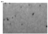
- FIG. 6 is a PL light emission pattern on the surface of a contact layer of the nitride semiconductor light emitting diode element of Example 2.
- FIG. 1 is a schematic cross-sectional view of a nitride semiconductor light-emitting diode element according to an embodiment which is an example of the nitride semiconductor light-emitting element of the present invention.
- the nitride semiconductor light-emitting diode device according to the embodiment includes a substrate 1, a first nitride semiconductor layer 2 provided on the substrate 1, and a first nitride semiconductor layer 2.
- the light emitting layer 3 provided and the second nitride semiconductor layer 4 provided on the light emitting layer 3 are provided.
- a first electrode 6 is formed on the first nitride semiconductor layer 2
- a second electrode 5 is formed on the second nitride semiconductor layer 4.
- the first nitride semiconductor layer 2, the light emitting layer 3, and the second nitride semiconductor layer 4 can be formed by, for example, the MOCVD (metal organic chemical vapor deposition) method.
- the second electrode 5 can be formed, for example, by vapor deposition.
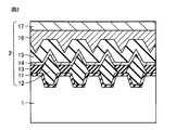
- FIG. 2 shows a schematic enlarged cross-sectional view of the substrate 1 and the first nitride semiconductor layer 2 shown in FIG.
- a buffer layer 11 is formed on the uneven surface of the substrate 1, and an oblique facet layer 12 is formed on the buffer layer 11 in the recess of the substrate 1.
- a first buried layer 13 is formed so as to fill a space between the oblique facet layers 12, and a high-concentration silicon doped layer 14 is formed on the surfaces of the oblique facet layers 12 and the first buried layer 13. Is formed.
- a dislocation reduction layer 15 is formed on the high-concentration silicon doped layer 14, and a second buried layer 16 is formed on the dislocation reduction layer 15. Furthermore, a conductive layer 17 is formed on the second buried layer 16.
- a silicon (Si) substrate, a sapphire (Al 2 O 3 ) substrate, a silicon carbide (SiC) substrate, a spinel (MgAl 2 O 4 ) substrate, or the like can be used.
- a sapphire substrate that is inexpensive and transparent as the substrate 1.
- the embodiment can improve the light extraction efficiency of the nitride semiconductor light-emitting diode element, Further, it becomes easier to form the oblique facet layer 12 during the initial growth.
- a GaN (gallium nitride) layer or an AlN (aluminum nitride) layer is preferably used.
- a GaN layer or an AlN layer is used for the buffer layer 11, a low dislocation nitride semiconductor layer can be formed on the buffer layer 11.
- an AlN layer is used as the buffer layer 11, the screw dislocations in the nitride semiconductor layer grown on the buffer layer 11 can be effectively reduced, and two different types of dislocations having different Burgers vectors. Both can be reduced. Therefore, the light emission efficiency of the nitride semiconductor light emitting device can be improved.
- a nitride semiconductor represented by an expression of Al x1 Ga y1 In z1 N (0 ⁇ x1 ⁇ 1, 0 ⁇ y1 ⁇ 1, 0 ⁇ z1 ⁇ 1, x1 + y1 + z1 ⁇ 0) is used. Can do.
- a nitride semiconductor represented by the formula of Al x2 Ga y2 In z2 N (0 ⁇ x2 ⁇ 1, 0 ⁇ y2 ⁇ 1, 0 ⁇ z2 ⁇ 1, x2 + y2 + z2 ⁇ 0) is used as the first buried layer 13.
- a nitride semiconductor represented by the formula of Al x2 Ga y2 In z2 N (0 ⁇ x2 ⁇ 1, 0 ⁇ y2 ⁇ 1, 0 ⁇ z2 ⁇ 1, x2 + y2 + z2 ⁇ 0) is used.
- the high-concentration silicon doped layer 14 for example, a nitride semiconductor represented by the formula of Al x3 Ga y3 In z3 N (0 ⁇ x3 ⁇ 1, 0 ⁇ y3 ⁇ 1, 0 ⁇ z3 ⁇ 1, x3 + y3 + z3 ⁇ 0) is used. Si doped at a high concentration of 2 ⁇ 10 19 atoms / cm 3 or more can be used.
- dislocation reduction layer 15 for example, a nitride semiconductor represented by the formula of Al x4 Ga y4 In z4 N (0 ⁇ x4 ⁇ 1, 0 ⁇ y4 ⁇ 1, 0 ⁇ z4 ⁇ 1, x4 + y4 + z4 ⁇ 0) is used. Can be used.
- the dislocation reduction layer 15 By forming the high-concentration silicon doped layer 14 doped with Si at a high concentration of 2 ⁇ 10 19 atoms / cm 3 or more, the three-dimensional growth of the nitride semiconductor layer is promoted on the high-concentration silicon doped layer 14, A dislocation reducing layer 15 having facets can be formed.
- the dislocation reduction layer 15 having oblique facets by three-dimensional growth the threading dislocation formed by the lattice mismatch between the substrate 1 and the nitride semiconductor layer formed on the substrate 1 is bent sideways. Therefore, the dislocation reduction layer 15 can function as a dislocation reduction layer. Note that the dislocation reduction layer 15 only needs to reduce the number of threading dislocations inherited by the second buried layer 16 on the dislocation reduction layer 15 by bending the threading dislocations from the high-concentration silicon doped layer 14. .
- the Si concentration diffuses while gradually decreasing the Si concentration in the growth direction (light emitting layer side), and is 1.5 ⁇ m from the surface on the light emitting layer 3 side of the high concentration silicon doped layer 14 toward the light emitting layer 3 side.
- the Si concentration at the location is preferably 1 ⁇ 10 17 / cm 3 or more.
- the dislocation reduction in the dislocation reduction layer 15 can be effectively performed.
- the dislocation reduction layer 15 is three-dimensionally grown on the high-concentration silicon doped layer 14, the dislocation reduction layer 15 does not need to be intentionally doped with Si. Further, the decrease in the Si concentration may be, for example, continuous and / or stepwise.
- the thickness of the high-concentration silicon doped layer 14 is preferably 0.5 ⁇ m or less. In this case, since excessive tensile stress is not applied to the high-concentration silicon doped layer 14, the crystallinity of the high-concentration silicon doped layer 14 can be improved.
- the molar ratio of ammonia (NH 3 ) to trimethylgallium (TMG) is set to 250 or less, so that the nitride semiconductor crystal constituting the dislocation reduction layer 15 can be formed. Since the grain size increases and the frequency of grain association decreases, dislocations can be effectively reduced.
- the Si concentration in the high-concentration silicon doped layer 14 can be determined by, for example, SIMS (secondary ion mass spectrometry).
- the direction of dislocations in the dislocation reduction layer 15 can be obtained by observing the dislocation reduction layer 15 with, for example, TEM (transmission electron microscope) or STEM (scanning transmission electron microscope).
- the second buried layer 16 for example, a nitride semiconductor represented by the formula of Al x5 Ga y5 In z5 N (0 ⁇ x5 ⁇ 1, 0 ⁇ y5 ⁇ 1, 0 ⁇ z5 ⁇ 1, x5 + y5 + z5 ⁇ 0) is used.
- the second buried layer 16 is doped with magnesium (Mg) from the viewpoint of flattening the surface of the second buried layer 16.
- Mg concentration doped in the second buried layer 16 is preferably 5 ⁇ 10 18 atoms / cm 3 or more and 5 ⁇ 10 19 atoms / cm 3 or less.
- the Mg concentration in the second buried layer 16 is 5 ⁇ 10 18 pieces / cm 3 or more and 5 ⁇ 10 19 pieces / cm 3 or less, the surface of the second buried layer 16 is made flatter. In addition, it is possible to effectively prevent white turbidity of the second embedded layer 16 and to have good crystallinity.
- the conductive layer 17 may be an n-type impurity in a nitride semiconductor represented by the formula Al x6 Ga y6 In z6 N (0 ⁇ x6 ⁇ 1, 0 ⁇ y6 ⁇ 1, 0 ⁇ z6 ⁇ 1, x6 + y6 + z6 ⁇ 0).
- a material doped with or the like can be used.
- the n-type impurity for example, Si and / or Ge (germanium) can be used.
- the light emitting layer 3 can be formed on the conductive layer 17.
- a nitride semiconductor represented by the formula of Al x7 Ga y7 In z7 N (0 ⁇ x7 ⁇ 1, 0 ⁇ y7 ⁇ 1, 0 ⁇ z7 ⁇ 1, x7 + y7 + z7 ⁇ 0) is used. it can.
- the wavelength of light emitted from the light emitting layer 3 can be appropriately adjusted by appropriately changing the composition of the nitride semiconductor constituting the light emitting layer 3 and changing the band gap.
- a multilayer film in which the band gap is periodically changed can be formed under the light emitting layer 3.
- the light emitting layer 3 may adopt either a single quantum well structure (SQW) or a multiple quantum well structure (MQW).
- a second nitride semiconductor layer 4 made of a p-type nitride semiconductor can be formed on the light emitting layer 3.
- the second nitride semiconductor layer 4 for example, a nitride represented by the formula of Al x8 Ga y8 In z8 N (0 ⁇ x8 ⁇ 1, 0 ⁇ y8 ⁇ 1, 0 ⁇ z8 ⁇ 1, x8 + y8 + z8 ⁇ 0).
- a semiconductor doped with a p-type impurity can be used.
- a p-type impurity for example, Mg and / or Zn (zinc) can be used.
- the second nitride semiconductor layer 4 may include a carrier block layer made of a p-type nitride semiconductor having a large band gap, and is made of a p-type nitride semiconductor doped with a p-type impurity at a high concentration.
- a contact layer may be included.
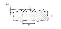
- a macro step 21 as shown in the schematic enlarged sectional view of FIG. 3 is formed.
- the macro step 21 is formed when the dislocation reducing layer 15 is buried with the second buried layer 16, and the light emitted from the light emitting layer 3 without reducing the light emission efficiency of the nitride semiconductor light emitting device by the macro step 21.
- the half-value width of can be increased.
- the macro step 21 is a surface inclined with respect to the growth surface, and is generated due to the arrangement of the high-concentration silicon doped layer 14.
- the emission wavelength of the phosphors is Although it is very broad, the emission wavelength of conventional blue light has a very narrow half-value width of about 20 nm, so the color reproducibility of blue light is poor, the color rendering is poor, and the safety to the human eye is low. There were problems such as.
- the emission wavelength of the blue light emitted from the light emitting layer 3 becomes broad due to the macro step 21, the color reproducibility of the blue light is good, the color rendering is good, and the safety to the human eye is improved.
- a high white LED device can be produced.
- the dominant light emission wavelength (single wavelength felt by human eyes) of the nitride semiconductor light emitting diode device of the embodiment is preferably 420 nm or more and 500 nm or less, and more preferably 430 nm or more and 470 nm or less.
- the human eye feels that the color reproducibility and color rendering of the blue light emitted from the light emitting layer 3 is good, and the safety for the human eye can be improved.
- the full width at half maximum of electroluminescence emission (light emitted from the light emitting layer 3 by current injection) of the nitride semiconductor light emitting diode element of the embodiment is preferably 25 nm or more.
- the human eye feels that the color reproducibility and color rendering of the blue light emitted from the light emitting layer 3 is good, and the safety for the human eye can be improved.
- the macro step 21 causes the surface to be very low in angle. Since there is an inclined portion, it is assumed that the emission wavelength of the portion is slightly shifted, the emission wavelength becomes broad, and the half width is widened.
- the height H of the macro step 21 is preferably 20 nm or more and 300 nm or less.
- the emission wavelength of the light emitted from the light emitting layer 3 can be broadened and the half width can be further increased.
- the height H of the macro step 21 is 300 nm or less, it tends to be possible to suppress a decrease in the light emission efficiency of the nitride semiconductor light-emitting diode element of the embodiment.
- the lateral width W of the macro step 21 is preferably 40 ⁇ m or more and 300 ⁇ m or less.
- the width W in the lateral direction of the macro step 21 is 40 ⁇ m or more, it tends to be possible to suppress a decrease in the light emission efficiency of the nitride semiconductor light emitting diode element of the embodiment.
- the width W in the horizontal direction of the macro step 21 is 300 ⁇ m or less, the emission wavelength of the light emitted from the light emitting layer 3 can be broadened and the half width can be further increased.
- the height H and the lateral width W of the macro step 21 can be measured by tracing the step of the surface of the conductive layer 17.
- a conductive oxide film such as ITO (Indium Tin Oxide) can be formed on the surface of the second nitride semiconductor layer 4.
- the second electrode 5 to be a p-electrode is formed on the conductive oxide film, the surface of the conductive layer 17 is exposed by mesa etching, and then the exposed surface of the conductive layer 17 is exposed.
- the first electrode 6 to be an n-electrode can be formed.
- a metal wire can be bonded to the first electrode 6 and the second electrode 5.
- irregularities were formed on the surface of the sapphire substrate 101.
- the unevenness on the surface of the sapphire substrate 101 was formed by patterning a resist on the surface of the flat sapphire substrate 101 using a stepper or the like and etching it by ICP (Inductively coupled plasma).
- the surface of the sapphire substrate 101 was nitrided by setting the sapphire substrate 101 in the sputtering film forming apparatus and flowing nitrogen gas into the sputtering film forming apparatus. Thereafter, a high frequency bias was applied to the metal Al target side while flowing 5 sccm of nitrogen gas in the sputtering film forming apparatus in a state where the temperature was 500 ° C. and the pressure in the sputtering film forming apparatus was maintained at 0.5 Pa. Thereby, as shown in the schematic cross-sectional view of FIG. 5, an AlN film 102 was formed on the surface of the sapphire substrate 101 by sputtering.
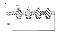
- the sapphire substrate 101 after the formation of the AlN film 102 was set in the reactor of the MOCVD apparatus. Thereafter, NH 3 as a group V source and TMG as a group III source are supplied into the reactor of the MOCVD apparatus at a temperature of 990 ° C., and as shown in the schematic cross-sectional view of FIG.
- An oblique facet layer 103 made of GaN having the oblique facets was grown by MOCVD. At this time, the angle of the oblique facet of the oblique facet layer 103 was approximately 60 ° with respect to the growth surface. Further, the oblique facet layer 103 grew only on the upper surface of the concave and convex portions on the surface of the sapphire substrate 101.
- NH 3 as a group V source and TMG as a group III source are supplied in the same manner as described above, and an oblique facet layer is formed by MOCVD as shown in the schematic sectional view of FIG.
- the depression between 103 was filled with the first buried layer 104 made of GaN.
- the thickness of the first embedded layer 104 was 0.5 ⁇ m, and the first embedded layer 104 was embedded partway through the oblique facet layer 103.
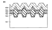
- a high-concentration silicon doped layer 105 was grown on the surfaces of the oblique facet layer 103 and the first buried layer 104 by MOCVD.
- a dislocation reduction layer 106 made of GaN having oblique facets was three-dimensionally grown on the surface of the high-concentration silicon doped layer 105 to a thickness of 3 ⁇ m by MOCVD.
- FIG. As shown in the schematic sectional view, a second buried layer 107 made of Mg-doped p-type GaN was grown on the surface of the dislocation reduction layer 106 by MOCVD.
- the molar ratio of NH 3 to TMG is adjusted to 440
- the Mg concentration in the second buried layer 107 is 2 ⁇ 10 19 atoms / cm 3
- the thickness of the second buried layer 107 is 2. 2 ⁇ m.
- a conductive layer 108 made of Si-doped n-type GaN was grown on the surface of the second buried layer 107 by MOCVD.
- the Si concentration in the conductive layer 108 was 5 ⁇ 10 18 / cm 3, and the thickness of the conductive layer 108 was 0.5 ⁇ m.
- Example 1 the template substrate of Example 1 in which the first nitride semiconductor layer was laminated on the sapphire substrate was produced. Note that each of the above temperatures indicates the thermocouple temperature in contact with the carbon susceptor.
- FIG. 12 shows the SIMS analysis results of the template substrate of Example 1
- FIG. 13 shows a CL (cathode luminescence) image of the template substrate of Example 1
- FIG. 14 shows the STEM of the template substrate of Example 1. Show the image.
- dislocations are bent in the lateral direction in the dislocation reduction layer 106, dislocations having different Burgers vectors meet, form a half loop, and disappear. Reduction was confirmed.
- dislocations that were conventionally about 1 ⁇ 10 8 pieces / cm 2 can be reduced to about 1 ⁇ 10 7 pieces / cm 2.
- the nitride semiconductor light-emitting diode element of Example 2 was fabricated by forming the light-emitting layer and the second nitride semiconductor layer on the template substrate of Example 1.
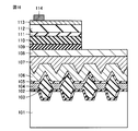
- the template substrate of Example 1 was set in the MOCVD apparatus, and as shown in the schematic cross-sectional view of FIG. 15, Si-doped n-type GaN was further grown by MOCVD at a temperature of 1255 ° C. The thickness of was set to 3 ⁇ m. Next, the temperature is lowered to 938 ° C., and a GaN layer having a thickness of 1.5 nm and an InGaN layer having a thickness of 1.5 nm are alternately grown for 20 periods one by one on the conductive layer 108. A superlattice layer 109 was grown by MOCVD.
- the temperature is lowered to 816 ° C., and a GaN barrier layer having a thickness of 7.5 nm and an InGaN well layer having a thickness of 3 nm are alternately grown for six periods one by one on the superlattice layer 109.
- the light emitting layer 110 was grown by MOCVD.
- a carrier block layer 111 having a three-layer structure of an undoped AlGaN layer, an Mg-doped p-type AlGaN layer, and an undoped AlGaN layer is grown on the light emitting layer 110 to a thickness of 20 nm by the MOCVD method. It was.
- an undoped GaN layer 112 having a thickness of 65 nm was grown on the carrier block layer 111 by MOCVD while maintaining the temperature.
- the temperature was raised to 1238 ° C., and a contact layer 113 made of Mg-doped p-type GaN having a thickness of 20 nm was grown on the undoped GaN layer 112 by MOCVD.
- the template substrate of Example 1 after the formation of the contact layer 113 is taken out from the MOCVD apparatus and annealed to activate Mg as a p-type impurity at 800 ° C. in an annealing furnace.
- the surface of the contact layer 113 was cleaned with acid.
- a pd electrode 114 is deposited as a p-electrode on the contact layer 113, and the surface of the conductive layer 108 is exposed by cutting the wafer edge with a diamond pen.
- the nitride semiconductor light-emitting diode device of Example 2 was completed.
- the pd electrode 114 of the nitride semiconductor light emitting diode element of Example 2 and the surface of the conductive layer 108 exposed by scraping the wafer edge are probed by a prober, and the nitride semiconductor light emitting diode element of Example 2 is obtained.
- the emission spectrum was measured from the back side of the light source using an instantaneous multi-photometry system and the intensity was measured with a photodetector.
- a template substrate produced in the same manner as in Example 1 except that the high-concentration silicon doped layer 105 was not formed was set in the MOCVD apparatus at the same time as the template substrate in Example 1, and the same as above. Under the conditions, a nitride semiconductor light emitting diode element of a comparative example was manufactured.
- the nitride semiconductor light-emitting diode device of Example 2 manufactured using the template substrate of Example 1 including the high-concentration silicon doped layer 105 is manufactured using the template substrate not including the high-concentration silicon doped layer 105. It was confirmed that the light output was improved by 12% compared to the nitride semiconductor light emitting diode element of the comparative example.
- the half width of electroluminescence emission at the current density of 10 A / cm 2 of the nitride semiconductor light-emitting diode element of Example 2 is 29.8 nm, and the current density of the nitride semiconductor light-emitting diode element of the comparative example at 10 A / cm 2 .
- the half width of electroluminescence emission was 21.5 nm. Therefore, it was confirmed that the full width at half maximum of electroluminescence emission of the nitride semiconductor light emitting diode element of Example 2 was very wide as compared with the nitride semiconductor light emitting diode element of the comparative example.
- the height was 20 nm or more and 100 nm or less, and the lateral direction The width was confirmed to be 40 ⁇ m or more and 150 ⁇ m or less.
- FIG. 17 shows a PL (Photo Luminescence) light emission pattern on the surface of the contact 113 of the nitride semiconductor light emitting diode element of Example 2. As shown in the PL emission pattern of FIG. 17, the edge of the macro step was observed.
- PL Photo Luminescence
- the nitride semiconductor light-emitting diode element of Example 2 in which the high-concentration silicon doped layer 105 is formed compared to the nitride semiconductor light-emitting diode element of the comparative example, the nitride semiconductor light-emitting diode element 105 is formed on the high-concentration silicon doped layer 105. It was confirmed that the threading dislocations can be reduced by the grown dislocation reduction layer 106, the emission wavelength becomes broad, and the half width of electroluminescence emission is widened.
- the color reproducibility in the blue region is good, the color rendering is good, and the safety to the human eye is high.
- a white LED device can be produced.
- a white LED device in which the light emission efficiency does not decrease and the luminous flux does not decrease can be manufactured.
- the present invention relates to a substrate, a first nitride semiconductor layer provided on the substrate, a light emitting layer provided on the first nitride semiconductor layer, and a second nitride provided on the light emitting layer.
- a first nitride semiconductor layer comprising: a high-concentration silicon-doped layer doped with silicon at a high concentration of 2 ⁇ 10 19 / cm 3 or more; and a threading dislocation on the high-concentration silicon-doped layer.
- a nitride semiconductor light-emitting device including a dislocation reducing layer for bending the substrate horizontally. With such a configuration, it is possible to provide a nitride semiconductor light emitting device having improved characteristics by reducing threading dislocations.
- the silicon concentration decreases from the high concentration silicon doped layer toward the light emitting layer side, and from the surface of the high concentration silicon doped layer toward the light emitting layer side. It is preferable that the silicon concentration at a position of 1.5 ⁇ m is 1 ⁇ 10 17 pieces / cm 3 or more. With such a configuration, it is possible to effectively reduce dislocations in the dislocation reducing layer.
- the thickness of the high concentration silicon doped layer is preferably 0.5 ⁇ m or less.
- a layer containing magnesium is disposed between the dislocation reducing layer and the light emitting layer.
- the surface of the layer containing magnesium can be made flat.
- the magnesium concentration in the layer containing magnesium is preferably 5 ⁇ 10 18 pieces / cm 3 or more and 5 ⁇ 10 19 pieces / cm 3 or less. By setting it as such a structure, the surface of the layer containing magnesium can be made flat.
- the nitride semiconductor light emitting device of the present invention preferably includes a macro step having a height of 20 nm to 300 nm and a lateral width of 40 ⁇ m to 300 ⁇ m.
- the nitride semiconductor light-emitting device of the present invention is a nitride semiconductor light-emitting diode device, and preferably has a dominant emission wavelength of 420 nm or more and 500 nm or less.
- the nitride semiconductor light emitting device of the present invention is a nitride semiconductor light emitting diode device, and preferably has a dominant emission wavelength of 430 nm or more and 470 nm or less.
- the half width of electroluminescence emission is 25 nm or more.
- the layer in contact with the substrate of the first nitride semiconductor layer is an aluminum nitride layer.
- the present invention provides a method for manufacturing the nitride semiconductor light-emitting device according to any one of the above, wherein a step of forming a first nitride semiconductor layer on a substrate, and a step on the first nitride semiconductor layer Forming a light emitting layer on the substrate, and forming a second nitride semiconductor layer provided on the light emitting layer, wherein the step of forming the first nitride semiconductor layer has a high concentration on the substrate.
- the present invention can be used for a nitride semiconductor light-emitting device, and can be particularly preferably used for a nitride semiconductor light-emitting diode device.
Landscapes
- Led Devices (AREA)
Abstract
Description
本発明は、基板と、基板上に設けられた第1の窒化物半導体層と、第1の窒化物半導体層上に設けられた発光層と、発光層上に設けられた第2の窒化物半導体層と、を備え、第1の窒化物半導体層は、シリコンが2×10¹⁹個/cm3以上の高濃度にドープされた高濃度シリコンドープ層と、高濃度シリコンドープ層上に貫通転位を横方向に曲げるための転位低減層とを含む窒化物半導体発光素子である。このような構成とすることにより、貫通転位を低減することにより特性を向上させた窒化物半導体発光素子を提供することができる。
Claims (5)
- 基板と、
前記基板上に設けられた第1の窒化物半導体層と、
前記第1の窒化物半導体層上に設けられた発光層と、
前記発光層上に設けられた第2の窒化物半導体層と、を備え、
前記第1の窒化物半導体層は、シリコンが2×10¹⁹個/cm3以上の高濃度にドープされた高濃度シリコンドープ層と、前記高濃度シリコンドープ層上に貫通転位を横方向に曲げるための転位低減層とを含む、窒化物半導体発光素子。 - 前記高濃度シリコンドープ層から前記発光層側に向かってシリコン濃度が低下していき、前記高濃度シリコンドープ層の前記発光層側の表面から前記発光層側に向かって1.5μmの箇所のシリコン濃度が1×10¹⁷個/cm3以上である、請求項1に記載の窒化物半導体発光素子。
- 前記高濃度シリコンドープ層の厚さは0.5μm以下である、請求項1または2に記載の窒化物半導体発光素子。
- 前記転位低減層と前記発光層との間にマグネシウムを含む層が配置されている、請求項1から3のいずれか1項に記載の窒化物半導体発光素子。
- 高さが20nm以上300nm以下であって、横方向の幅が40μm以上300μm以下のマクロステップを含む、請求項1から4のいずれか1項に記載の窒化物半導体発光素子。
Priority Applications (3)
| Application Number | Priority Date | Filing Date | Title |
|---|---|---|---|
| JP2014543179A JP6181661B2 (ja) | 2012-10-22 | 2013-09-05 | 窒化物半導体発光素子 |
| CN201380040831.5A CN104541381B (zh) | 2012-10-22 | 2013-09-05 | 氮化物半导体发光元件 |
| US14/400,625 US9450150B2 (en) | 2012-10-22 | 2013-09-05 | Nitride semiconductor light-emitting element |
Applications Claiming Priority (2)
| Application Number | Priority Date | Filing Date | Title |
|---|---|---|---|
| JP2012232681 | 2012-10-22 | ||
| JP2012-232681 | 2012-10-22 |
Publications (1)
| Publication Number | Publication Date |
|---|---|
| WO2014065019A1 true WO2014065019A1 (ja) | 2014-05-01 |
Family
ID=50544400
Family Applications (1)
| Application Number | Title | Priority Date | Filing Date |
|---|---|---|---|
| PCT/JP2013/073904 Ceased WO2014065019A1 (ja) | 2012-10-22 | 2013-09-05 | 窒化物半導体発光素子 |
Country Status (4)
| Country | Link |
|---|---|
| US (1) | US9450150B2 (ja) |
| JP (1) | JP6181661B2 (ja) |
| CN (1) | CN104541381B (ja) |
| WO (1) | WO2014065019A1 (ja) |
Cited By (4)
| Publication number | Priority date | Publication date | Assignee | Title |
|---|---|---|---|---|
| WO2015194382A1 (ja) * | 2014-06-17 | 2015-12-23 | エルシード株式会社 | 発光素子の製造方法及び発光素子 |
| JP5866044B1 (ja) * | 2014-11-13 | 2016-02-17 | エルシード株式会社 | 発光素子の製造方法及び発光素子 |
| JPWO2016047386A1 (ja) * | 2014-09-22 | 2017-07-06 | シャープ株式会社 | 窒化物半導体発光素子 |
| US9853183B2 (en) | 2014-06-17 | 2017-12-26 | El-Seed Corporation | Method for manufacturing light emitting element and light emitting element |
Families Citing this family (2)
| Publication number | Priority date | Publication date | Assignee | Title |
|---|---|---|---|---|
| US9873170B2 (en) * | 2015-03-24 | 2018-01-23 | Nichia Corporation | Method of manufacturing light emitting element |
| CN115911197B (zh) * | 2022-10-27 | 2025-08-19 | 安徽三安光电有限公司 | 一种发光二极管的外延结构及其制备方法 |
Citations (7)
| Publication number | Priority date | Publication date | Assignee | Title |
|---|---|---|---|---|
| JP2003277196A (ja) * | 2002-03-26 | 2003-10-02 | Hitachi Cable Ltd | 窒化物半導体結晶の製造方法及び窒化物半導体ウエハ並びに窒化物半導体デバイス |
| JP2004047764A (ja) * | 2002-07-12 | 2004-02-12 | Hitachi Cable Ltd | 窒化物半導体の製造方法および半導体ウェハならびに半導体デバイス |
| JP2006060164A (ja) * | 2004-08-24 | 2006-03-02 | National Institute Of Advanced Industrial & Technology | 窒化物半導体デバイスおよび窒化物半導体結晶成長方法 |
| JP2006140357A (ja) * | 2004-11-12 | 2006-06-01 | Mitsubishi Cable Ind Ltd | 窒化物半導体発光素子 |
| JP2006313771A (ja) * | 2005-05-06 | 2006-11-16 | Showa Denko Kk | Iii族窒化物半導体素子用エピタキシャル基盤 |
| JP2008141005A (ja) * | 2006-12-01 | 2008-06-19 | Eudyna Devices Inc | 半導体基板、半導体装置およびその製造方法 |
| JP2009224704A (ja) * | 2008-03-18 | 2009-10-01 | Sumitomo Electric Ind Ltd | 窒化物系半導体発光素子、エピタキシャルウエハ、及び窒化物系半導体発光素子を作製する方法 |
Family Cites Families (21)
| Publication number | Priority date | Publication date | Assignee | Title |
|---|---|---|---|---|
| JP2751963B2 (ja) | 1992-06-10 | 1998-05-18 | 日亜化学工業株式会社 | 窒化インジウムガリウム半導体の成長方法 |
| JP3592553B2 (ja) * | 1998-10-15 | 2004-11-24 | 株式会社東芝 | 窒化ガリウム系半導体装置 |
| KR100580751B1 (ko) * | 2004-12-23 | 2006-05-15 | 엘지이노텍 주식회사 | 질화물 반도체 발광소자 및 그 제조방법 |
| TWI248691B (en) * | 2005-06-03 | 2006-02-01 | Formosa Epitaxy Inc | Light emitting diode and method of fabricating thereof |
| KR20080070750A (ko) * | 2005-12-14 | 2008-07-30 | 쇼와 덴코 가부시키가이샤 | 질화갈륨계 화합물 반도체 발광 소자 및 그 제조 방법, 및 질화갈륨계 화합물 반도체 발광 소자로 이루어진 램프 |
| JP5165264B2 (ja) * | 2007-03-22 | 2013-03-21 | 浜松ホトニクス株式会社 | 窒化物半導体基板 |
| JP5223439B2 (ja) * | 2007-05-28 | 2013-06-26 | ソニー株式会社 | 半導体発光素子 |
| JP2009016467A (ja) * | 2007-07-03 | 2009-01-22 | Sony Corp | 窒化ガリウム系半導体素子及びこれを用いた光学装置並びにこれを用いた画像表示装置 |
| KR101449000B1 (ko) * | 2007-09-06 | 2014-10-13 | 엘지이노텍 주식회사 | 반도체 발광소자 및 그 제조방법 |
| KR101459754B1 (ko) * | 2007-09-06 | 2014-11-13 | 엘지이노텍 주식회사 | 반도체 발광소자 및 그 제조방법 |
| JP4730422B2 (ja) * | 2008-10-24 | 2011-07-20 | 住友電気工業株式会社 | Iii族窒化物半導体電子デバイス、iii族窒化物半導体電子デバイスを作製する方法、及びiii族窒化物半導体エピタキシャルウエハ |
| JP5287406B2 (ja) * | 2009-03-24 | 2013-09-11 | 豊田合成株式会社 | Iii族窒化物半導体の製造方法 |
| JP5489117B2 (ja) * | 2009-09-01 | 2014-05-14 | シャープ株式会社 | 窒化物半導体素子、窒化物半導体素子の製造方法、窒化物半導体層の製造方法および窒化物半導体発光素子 |
| US8044422B2 (en) * | 2009-11-25 | 2011-10-25 | Huga Optotech Inc. | Semiconductor light emitting devices with a substrate having a plurality of bumps |
| DE102009060750B4 (de) * | 2009-12-30 | 2025-04-10 | OSRAM Opto Semiconductors Gesellschaft mit beschränkter Haftung | Optoelektronischer Halbleiterchip und Verfahren zu dessen Herstellung |
| WO2011102411A1 (ja) * | 2010-02-19 | 2011-08-25 | シャープ株式会社 | 窒化物半導体発光素子および窒化物半導体発光素子の製造方法 |
| US8765509B2 (en) * | 2010-09-30 | 2014-07-01 | Toyoda Gosei Co., Ltd. | Method for producing group III nitride semiconductor light-emitting device |
| WO2012090818A1 (ja) * | 2010-12-29 | 2012-07-05 | シャープ株式会社 | 窒化物半導体構造、窒化物半導体発光素子、窒化物半導体トランジスタ素子、窒化物半導体構造の製造方法および窒化物半導体素子の製造方法 |
| KR101810609B1 (ko) * | 2011-02-14 | 2017-12-20 | 삼성전자주식회사 | 반도체 소자 및 그 제조방법 |
| JP5813448B2 (ja) * | 2011-10-07 | 2015-11-17 | シャープ株式会社 | 窒化物半導体素子の製造方法 |
| JP5661660B2 (ja) * | 2012-02-07 | 2015-01-28 | 株式会社東芝 | 半導体発光素子 |
-
2013
- 2013-09-05 US US14/400,625 patent/US9450150B2/en not_active Expired - Fee Related
- 2013-09-05 JP JP2014543179A patent/JP6181661B2/ja not_active Expired - Fee Related
- 2013-09-05 WO PCT/JP2013/073904 patent/WO2014065019A1/ja not_active Ceased
- 2013-09-05 CN CN201380040831.5A patent/CN104541381B/zh not_active Expired - Fee Related
Patent Citations (7)
| Publication number | Priority date | Publication date | Assignee | Title |
|---|---|---|---|---|
| JP2003277196A (ja) * | 2002-03-26 | 2003-10-02 | Hitachi Cable Ltd | 窒化物半導体結晶の製造方法及び窒化物半導体ウエハ並びに窒化物半導体デバイス |
| JP2004047764A (ja) * | 2002-07-12 | 2004-02-12 | Hitachi Cable Ltd | 窒化物半導体の製造方法および半導体ウェハならびに半導体デバイス |
| JP2006060164A (ja) * | 2004-08-24 | 2006-03-02 | National Institute Of Advanced Industrial & Technology | 窒化物半導体デバイスおよび窒化物半導体結晶成長方法 |
| JP2006140357A (ja) * | 2004-11-12 | 2006-06-01 | Mitsubishi Cable Ind Ltd | 窒化物半導体発光素子 |
| JP2006313771A (ja) * | 2005-05-06 | 2006-11-16 | Showa Denko Kk | Iii族窒化物半導体素子用エピタキシャル基盤 |
| JP2008141005A (ja) * | 2006-12-01 | 2008-06-19 | Eudyna Devices Inc | 半導体基板、半導体装置およびその製造方法 |
| JP2009224704A (ja) * | 2008-03-18 | 2009-10-01 | Sumitomo Electric Ind Ltd | 窒化物系半導体発光素子、エピタキシャルウエハ、及び窒化物系半導体発光素子を作製する方法 |
Cited By (4)
| Publication number | Priority date | Publication date | Assignee | Title |
|---|---|---|---|---|
| WO2015194382A1 (ja) * | 2014-06-17 | 2015-12-23 | エルシード株式会社 | 発光素子の製造方法及び発光素子 |
| US9853183B2 (en) | 2014-06-17 | 2017-12-26 | El-Seed Corporation | Method for manufacturing light emitting element and light emitting element |
| JPWO2016047386A1 (ja) * | 2014-09-22 | 2017-07-06 | シャープ株式会社 | 窒化物半導体発光素子 |
| JP5866044B1 (ja) * | 2014-11-13 | 2016-02-17 | エルシード株式会社 | 発光素子の製造方法及び発光素子 |
Also Published As
| Publication number | Publication date |
|---|---|
| US9450150B2 (en) | 2016-09-20 |
| US20150137173A1 (en) | 2015-05-21 |
| CN104541381B (zh) | 2017-12-01 |
| CN104541381A (zh) | 2015-04-22 |
| JPWO2014065019A1 (ja) | 2016-09-08 |
| JP6181661B2 (ja) | 2017-08-16 |
Similar Documents
| Publication | Publication Date | Title |
|---|---|---|
| TWI447953B (zh) | 半導體發光裝置及其製造方法 | |
| JP4307113B2 (ja) | 半導体発光素子およびその製造方法 | |
| JP5108532B2 (ja) | 窒化物半導体発光装置 | |
| US7187007B2 (en) | Nitride semiconductor device and method of manufacturing the same | |
| TWI603500B (zh) | Nitride semiconductor light-emitting device | |
| JP5549338B2 (ja) | 紫外光放射用窒素化合物半導体ledおよびその製造方法 | |
| TWI381547B (zh) | 三族氮化合物半導體發光二極體及其製造方法 | |
| US20100133506A1 (en) | Nitride semiconductor light emitting element and method for manufacturing nitride semiconductor | |
| JP2011517098A (ja) | 半極性(Al,In,Ga,B)Nベースの発光ダイオードの製造のための方法 | |
| JP6181661B2 (ja) | 窒化物半導体発光素子 | |
| JP7844440B2 (ja) | Ledデバイス及びledデバイスの製造方法 | |
| JP2008103665A (ja) | 窒化物半導体デバイス及びその製造方法 | |
| JP5082672B2 (ja) | Iii族窒化物系化合物半導体の製造方法及び発光素子 | |
| JP2008118049A (ja) | GaN系半導体発光素子 | |
| JP2006237281A (ja) | 半導体装置の製造方法 | |
| WO2008056632A1 (en) | GaN SEMICONDUCTOR LIGHT EMITTING ELEMENT | |
| TW201528441A (zh) | 氮化物半導體元件之製造方法 | |
| JPH11354843A (ja) | Iii族窒化物系量子ドット構造の製造方法およびその用途 | |
| JP2013187296A (ja) | 窒化物半導体素子形成用ウエハ、窒化物半導体素子形成用ウエハの製造方法、窒化物半導体素子、および窒化物半導体素子の製造方法 | |
| JP2007036174A (ja) | 窒化ガリウム系発光ダイオード | |
| TWI545798B (zh) | Nitride semiconductor light emitting device and manufacturing method thereof | |
| JP2008227103A (ja) | GaN系半導体発光素子 | |
| CN110050330B (zh) | Iii族氮化物半导体 | |
| US20150228847A1 (en) | High-luminance nitride light-emitting device and method for manufacturing same | |
| KR20080026882A (ko) | 질화물 반도체 발광소자 및 그 제조 방법 |
Legal Events
| Date | Code | Title | Description |
|---|---|---|---|
| 121 | Ep: the epo has been informed by wipo that ep was designated in this application |
Ref document number: 13848978 Country of ref document: EP Kind code of ref document: A1 |
|
| ENP | Entry into the national phase |
Ref document number: 2014543179 Country of ref document: JP Kind code of ref document: A |
|
| WWE | Wipo information: entry into national phase |
Ref document number: 14400625 Country of ref document: US |
|
| NENP | Non-entry into the national phase |
Ref country code: DE |
|
| 122 | Ep: pct application non-entry in european phase |
Ref document number: 13848978 Country of ref document: EP Kind code of ref document: A1 |