WO2015194382A1 - 発光素子の製造方法及び発光素子 - Google Patents
発光素子の製造方法及び発光素子 Download PDFInfo
- Publication number
- WO2015194382A1 WO2015194382A1 PCT/JP2015/066149 JP2015066149W WO2015194382A1 WO 2015194382 A1 WO2015194382 A1 WO 2015194382A1 JP 2015066149 W JP2015066149 W JP 2015066149W WO 2015194382 A1 WO2015194382 A1 WO 2015194382A1
- Authority
- WO
- WIPO (PCT)
- Prior art keywords
- layer
- light emitting
- light
- crystal nuclei
- buffer layer
- Prior art date
Links
Images


Classifications
-
- H—ELECTRICITY
- H01—ELECTRIC ELEMENTS
- H01L—SEMICONDUCTOR DEVICES NOT COVERED BY CLASS H10
- H01L33/00—Semiconductor devices with at least one potential-jump barrier or surface barrier specially adapted for light emission; Processes or apparatus specially adapted for the manufacture or treatment thereof or of parts thereof; Details thereof
- H01L33/02—Semiconductor devices with at least one potential-jump barrier or surface barrier specially adapted for light emission; Processes or apparatus specially adapted for the manufacture or treatment thereof or of parts thereof; Details thereof characterised by the semiconductor bodies
- H01L33/20—Semiconductor devices with at least one potential-jump barrier or surface barrier specially adapted for light emission; Processes or apparatus specially adapted for the manufacture or treatment thereof or of parts thereof; Details thereof characterised by the semiconductor bodies with a particular shape, e.g. curved or truncated substrate
- H01L33/22—Roughened surfaces, e.g. at the interface between epitaxial layers
-
- H—ELECTRICITY
- H01—ELECTRIC ELEMENTS
- H01L—SEMICONDUCTOR DEVICES NOT COVERED BY CLASS H10
- H01L33/00—Semiconductor devices with at least one potential-jump barrier or surface barrier specially adapted for light emission; Processes or apparatus specially adapted for the manufacture or treatment thereof or of parts thereof; Details thereof
- H01L33/02—Semiconductor devices with at least one potential-jump barrier or surface barrier specially adapted for light emission; Processes or apparatus specially adapted for the manufacture or treatment thereof or of parts thereof; Details thereof characterised by the semiconductor bodies
- H01L33/26—Materials of the light emitting region
- H01L33/30—Materials of the light emitting region containing only elements of group III and group V of the periodic system
- H01L33/32—Materials of the light emitting region containing only elements of group III and group V of the periodic system containing nitrogen
-
- H—ELECTRICITY
- H01—ELECTRIC ELEMENTS
- H01L—SEMICONDUCTOR DEVICES NOT COVERED BY CLASS H10
- H01L33/00—Semiconductor devices with at least one potential-jump barrier or surface barrier specially adapted for light emission; Processes or apparatus specially adapted for the manufacture or treatment thereof or of parts thereof; Details thereof
- H01L33/36—Semiconductor devices with at least one potential-jump barrier or surface barrier specially adapted for light emission; Processes or apparatus specially adapted for the manufacture or treatment thereof or of parts thereof; Details thereof characterised by the electrodes
- H01L33/38—Semiconductor devices with at least one potential-jump barrier or surface barrier specially adapted for light emission; Processes or apparatus specially adapted for the manufacture or treatment thereof or of parts thereof; Details thereof characterised by the electrodes with a particular shape
Definitions
- the present invention relates to a method for manufacturing a light emitting element and a light emitting element.
- an LED element comprising a diffractive surface in which concave or convex portions are formed at a period, and an Al reflective film that is formed on the back side of the substrate and reflects light diffracted by the diffractive surface and re-enters the diffractive surface.
- the light transmitted by the diffraction action is re-incident on the diffraction surface, and the light is transmitted again using the diffraction action on the diffraction surface, so that the light can be extracted outside the element in a plurality of modes.
- the crystal quality of the group III nitride semiconductor greatly changes due to the pitch of the concave and convex portions when a group III nitride semiconductor is grown on the surface thereafter. Turned out to be.
- the present invention has been made in view of the above circumstances, and the object of the present invention is to use a substrate having a concave or convex portion formed at a period in which the surface forms a diffractive surface, even if the substrate has a concave and convex pitch III. It is an object of the present invention to provide a method for manufacturing a light emitting device capable of suppressing a change in crystal quality of a group nitride semiconductor and a light emitting device manufactured by this manufacturing method.
- a semiconductor stacked portion including a light emitting layer and made of a group III nitride semiconductor has a convex portion with a period larger than the optical wavelength of light emitted from the light emitting layer and smaller than the coherent length of the light.
- a method for manufacturing a light emitting device in which a plurality of crystal nuclei having facet surfaces and spaced apart from each other are grown, and a planarization layer is grown on a buffer layer in which the plurality of crystal nuclei are formed.
- the plurality of crystal nuclei may have a flat upper surface.
- the buffer layer may be formed by sputtering using AlN as a target.
- the plurality of crystal nuclei may be grown to a height of 900 nm or less.
- the semiconductor light-emitting device is manufactured by the method for manufacturing a light-emitting element, and the semiconductor stacked portion includes the buffer layer, the plurality of crystal nuclei, and the planarization layer, and the plurality of crystal nuclei are The oxygen concentration may be higher than that of the planarizing layer.
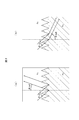
- FIG. 1 is a schematic cross-sectional view of an LED element showing an embodiment of the present invention.
- 2A and 2B are explanatory diagrams showing the diffraction action of light at the interface having different refractive indexes, where FIG. 2A shows a state of reflection at the interface, and FIG. 2B shows a state of transmission through the interface.
- 3A and 3B show a sapphire substrate, in which FIG. 3A is a schematic perspective view, FIG. 3B is a schematic explanatory view showing an AA section, and FIG. 3C is a schematic enlarged explanatory view.
- FIG. 4 is an example of a chart showing a change in growth temperature in the early stage of growth of the group III nitride semiconductor.
- FIG. 4 is an example of a chart showing a change in growth temperature in the early stage of growth of the group III nitride semiconductor.
- FIG. 5 is a schematic plan view showing the formation state of crystal nuclei.
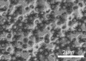
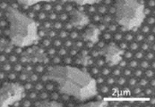
- FIG. 6 is an SEM image of the sample body A.
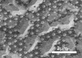
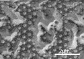
- FIG. 7 is an SEM image of the sample body B.
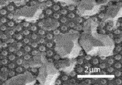
- FIG. 8 is an SEM image of the sample body C.
- FIG. 9 is an SEM image of the sample body D.
- FIG. 10 is an SEM image of the sample body E.
- FIG. 11 is an SEM image of the sample body F.
- FIG. 12 is a graph showing the relationship between the pitch of convex portions and the threading dislocation density for a sample body in which crystal nuclei are formed and a sample body in which crystal nuclei are not formed.
- FIG. 12 is a graph showing the relationship between the pitch of convex portions and the threading dislocation density for a sample body in which crystal nuclei are formed and a sample body in which crystal nuclei are not formed.
- FIG. 13 is an example of a chart showing a change in growth temperature in the early stage of growth of a group III nitride semiconductor when no crystal nucleus is formed.
- FIG. 14 is a graph showing the relationship between crystal nucleus height and threading dislocation density.
- FIG. 15 is a schematic cross-sectional view of an LED element showing a modification.
- FIG. 1 is a schematic cross-sectional view of an LED element showing an embodiment of the present invention.
- the LED element 1 includes a sapphire substrate 2 on which a semiconductor stacked portion 19 made of a group III nitride semiconductor layer is formed.
- the LED element 1 is a flip chip type, and light is mainly extracted from the back side of the sapphire substrate 2.
- the semiconductor stacked unit 19 includes a buffer layer 10, a planarizing layer 12, an n-type GaN layer 13, a light emitting layer 14, an electron blocking layer 16, and a p-type GaN layer 18 in this order from the sapphire substrate 2 side.
- a plurality of crystal nuclei 11 are formed on the buffer layer 10.
- a p-side electrode 27 is formed on the p-type GaN layer 18, and an n-side electrode 28 is formed on the n-type GaN layer 12.
- the buffer layer 10 is formed on the surface of the sapphire substrate 2 and is made of AlN.
- the buffer layer 10 is formed along the substrate surface including the convex portion 2 c, and the unevenness of the sapphire substrate 2 is inherited on the surface of the buffer layer 10.
- the buffer layer 10 is formed by MOCVD (Metal-Organic-Chemical-Vapor-Deposition) method, but a sputtering method can also be used. When the sputtering method is used, it is preferable that the sputtering is not reactive reactive with Al as a target but AlN as a target.
- the planarization layer 12 is formed on the buffer layer 10 and is made of undoped u-GaN.
- the n-type GaN layer 13 as the first conductivity type layer is formed on the planarization layer 12 and is made of n-GaN.
- the light emitting layer 14 is formed on the n-type GaN layer 13 and is made of GalnN / GaN, and emits blue light by injection of electrons and holes.
- blue light refers to light having a peak wavelength of 430 nm or more and 480 nm or less, for example. In the present embodiment, the peak wavelength of light emission of the light emitting layer 14 is 450 nm.
- the electron block layer 16 is formed on the light emitting layer 14 and is made of p-AIGaN.
- the p-type GaN layer 18 as the second conductivity type layer is formed on the electron block layer 16 and is made of p-GaN.
- the buffer layer 10 to the p-type GaN layer 18 are formed by epitaxial growth of a group III nitride semiconductor.
- the active layer is formed by recombination of electrons and holes.
- the layer structure of the semiconductor layer is arbitrary as long as it emits light.
- the surface of the sapphire substrate 2 forms a vertical moth-eye surface 2a, and the surface of the sapphire substrate 2 is formed with a flat portion 2b and a plurality of convex portions 2c periodically formed on the flat portion 2b.
- the semiconductor laminated portion 19 is formed without a gap around each convex portion 2c.
- the shape of each convex portion 2c may be a truncated cone shape such as a cone or a polygonal pyramid, or a truncated cone shape such as a truncated cone or a truncated polygonal truncated cone.
- Each convex portion 2 c is designed to diffract light emitted from the light emitting layer 14.
- the light verticalizing action can be obtained by the convex portions 2c arranged periodically.
- the light verticalizing action means that the light intensity distribution is reflected and transmitted with respect to the interface between the sapphire substrate 2 and the semiconductor laminated portion 19 rather than before the light is incident on the vertical moth-eye surface. It is biased in the vertical direction.
- FIG. 2A and 2B are explanatory diagrams showing the diffraction action of light at the interface having different refractive indexes, where FIG. 2A shows a state of reflection at the interface, and FIG. 2B shows a state of transmission through the interface.
- n1 is the refractive index of the medium on the incident side
- ⁇ is the wavelength of the incident light
- m is an integer.
- n1 is the refractive index of the group III nitride semiconductor. As shown in FIG. 2A, light incident on the interface is reflected at a reflection angle ⁇ ref that satisfies the above equation (1).
- n2 is the refractive index of the medium on the exit side
- m ′ is an integer.
- n2 is the refractive index of sapphire.
- FIG. 2B light incident on the interface is transmitted at a transmission angle ⁇ out that satisfies the above equation (2).
- the period of the surface of the sapphire substrate 2 is the optical wavelength inside the element ( ⁇ / n1) and ( ⁇ / n2) must be larger. Therefore, the surface of the sapphire substrate 2 is set to have a period longer than ( ⁇ / n1) or ( ⁇ / n2) so that diffracted light exists.
- the p-side electrode 27 includes a diffusion electrode 21 formed on the p-type GaN layer 18, a dielectric multilayer film 22 formed in a predetermined region on the diffusion electrode 21, and a dielectric multilayer film. 22 and a metal electrode 23 formed on the substrate 22.
- the diffusion electrode 21 is formed on the entire surface of the p-type GaN layer 18 and is made of a transparent material such as ITO (Indium Tin Oxide).
- the dielectric multilayer film 22 is configured by repeating a plurality of pairs of a first material and a second material having different refractive indexes.
- the dielectric multilayer film 22 may be made of ZrO 2 (refractive index: 2.18) as the first material, SiO 2 (refractive index: 1.46) as the second material, and five pairs.
- the dielectric multilayer film 22 may be formed using a material different from ZrO 2 and SiO 2.
- AlN reffractive index: 2.18
- Nb 2 O 3 reffractive index: 2.4
- Ta 2 O 3 reffractive index: 2.35
- the metal electrode 23 covers the dielectric multilayer film 22 and is made of a metal material such as Al.
- the metal electrode 23 is electrically connected to the diffusion electrode 21 through a via hole 22 a formed in the dielectric multilayer film 22.
- the n-side electrode 28 is formed on the exposed n-type GaN layer 12 by etching the n-type GaN layer 12 from the p-type GaN layer 18.
- the n-side electrode 28 includes a diffusion electrode 24 formed on the n-type GaN layer 12, a dielectric multilayer film 25 formed in a predetermined region on the diffusion electrode 24, and a metal formed on the dielectric multilayer film 25. Electrode 26.
- the diffusion electrode 24 is formed on the entire surface of the n-type GaN layer 12 and is made of a transparent material such as ITO (Indium Tin Oxide).
- the dielectric multilayer film 25 is configured by repeating a plurality of pairs of a first material and a second material having different refractive indexes.
- the first material can be ZrO 2 (refractive index: 2.18)
- the second material can be SiO 2 (refractive index: 1.46)
- the number of pairs can be five.
- the dielectric multilayer film 25 may be formed using a material different from ZrO 2 and SiO 2 , for example, AlN (refractive index: 2.18), Nb 2 O 3 (refractive index: 2.4), Ta 2 O 3 (refractive index: 2.35) or the like may be used.
- the metal electrode 26 covers the dielectric multilayer film 25 and is made of a metal material such as Al. The metal electrode 26 is electrically connected to the diffusion electrode 24 through a via hole 25 a formed in the dielectric multilayer film 25.
- the p-side electrode 27 and the n-side electrode 28 form a reflecting portion.
- the p-side electrode 27 and the n-side electrode 28 each have a higher reflectance as the angle is closer to the vertical.
- the light reflected by the vertical moth-eye surface 2a of the sapphire substrate 2 and changed in angle toward the perpendicular to the interface is incident. . That is, the intensity distribution of light incident on the reflecting portion is biased toward the vertical as compared with the case where the surface of the sapphire substrate 2 is a flat surface.
- FIG. 3A and 3B show a sapphire substrate, in which FIG. 3A is a schematic perspective view, FIG. 3B is a schematic explanatory view showing an AA section, and FIG. 3C is a schematic enlarged explanatory view.
- the verticalized moth-eye surface 2a has an intersection of virtual triangular lattices at a predetermined period so that the center of each convex portion 2c is the position of the apex of the regular triangle in plan view. It is formed in alignment with.
- each convex part 2c is larger than the optical wavelength of the light emitted from the light emitting layer 14, and smaller than the coherent length of the said light.
- the period here means the distance of the peak position of the height in the adjacent convex part 2c.
- the optical wavelength means a value obtained by dividing the actual wavelength by the refractive index.
- the coherent length corresponds to a distance until the periodic vibrations of the waves cancel each other and the coherence disappears due to the difference in the individual wavelengths of the photon group having a predetermined spectral width.
- the period of each convex part 2c is 1 time or more of the optical wavelength, and the diffractive action gradually works effectively for incident light having an angle greater than or equal to the critical angle, and is 2 of the optical wavelength of the light emitted from the light emitting layer 14. If it is larger than twice, the number of transmission modes and reflection modes is sufficiently increased, which is preferable. Moreover, it is preferable that the period of each convex part 2c is below half of the coherent length of the light emitted from the light emitting layer 14.
- the length of one side of an equilateral triangle forming a virtual triangular lattice is 460 nm, and the period of each convex portion 2c is 460 nm. Since the wavelength of light emitted from the light emitting layer 14 is 450 nm and the refractive index of the group III nitride semiconductor layer is 2.4, the optical wavelength is 187.5 nm. Moreover, since the half width of the light emitted from the light emitting layer 14 is 27 nm, the coherent length of the light is 7500 nm. That is, the period of the verticalized moth-eye surface 2a is greater than twice the optical wavelength of the light emitting layer 14 and less than or equal to half the coherent length.
- each convex portion 2c of the verticalized moth-eye surface 2a includes a side surface 2d extending upward from the flat portion 2b, and a center side of the convex portion 2c from the upper end of the side surface 2d. And a curved upper surface 2f formed continuously with the curved portion 2e.
- the curved portion 2e is formed by dropping the corners by wet etching of the convex portion 2c before the curved portion 2e formed with the corners formed by the meeting portions of the side surface 2d and the upper surface 2f. Note that wet etching may be performed until the flat upper surface 2f disappears and the entire upper side of the convex portion 2c becomes the curved portion 2e.
- each convex part 2c has a base end diameter of 380 nm and a height of 400 nm.
- the vertical moth-eye surface 2a of the sapphire substrate 2 is a flat portion 2b in addition to the convex portions 2c.
- the manufacturing method of this embodiment includes a mask layer forming step, a resist film forming step, a pattern forming step, a residual film removing step, a resist alteration step, a mask layer etching step, and a sapphire substrate etching step, A mask layer removing step and a curved portion forming step.
- a sapphire substrate 2 before processing is prepared, and the sapphire substrate 2 is cleaned with a predetermined cleaning liquid prior to etching.
- a mask layer is formed on the sapphire substrate 2 (mask layer forming step).
- the mask layer has a SiO 2 layer on the sapphire substrate 2 and a Ni layer on the SiO 2 layer.
- the mask layer may be a single layer.
- the mask layer is formed by a sputtering method, a vacuum evaporation method, a CVD method, or the like.
- a resist film is formed on the mask layer (resist film forming step).
- a thermoplastic resin such as an epoxy resin is used as the resist film, and the resist film is formed to have a uniform thickness by a spin coating method.
- a photocurable resin can be used in addition to the thermoplastic resin.
- the resist film is heated and softened together with the sapphire substrate 2, and the resist film is pressed with a mold. An uneven structure is formed on the contact surface of the mold, and the resist film is deformed along the uneven structure. Thereafter, the resist film is cooled and cured together with the sapphire substrate 2 while keeping the pressed state. Then, by separating the mold from the resist film, the concavo-convex structure is transferred to the resist film (pattern forming step).
- the period of the concavo-convex structure is 460 nm.
- the diameter of the convex part of an uneven structure is 100 nm or more and 300 nm or less, for example, 230 nm. Further, the height of the convex portion is not less than 100 nm and not more than 300 nm, for example, 250 nm. In this state, a residual film is formed in the concave portion of the resist film.
- the sapphire substrate 2 on which the resist film is formed as described above is attached to the substrate holding table of the plasma etching apparatus. Then, for example, the residual film is removed by plasma ashing to expose the mask layer (residual film removing step).
- O 2 gas is used as a processing gas for plasma ashing.
- the resist film is exposed to plasma under alteration conditions to alter the resist film and increase the etching selectivity (resist alteration process).
- Ar gas is used as a process gas for modifying the resist film.
- the bias output of the power source in the plasma etching apparatus for inducing plasma to the sapphire substrate 2 side is set to be lower than the etching condition described later.
- the mask layer is etched using the resist film exposed to plasma under the etching conditions and having a high etching selectivity as a mask (mask layer etching step).
- Ar gas is used as a processing gas for etching the resist film. Thereby, a pattern is formed in the mask layer.
- the processing gas, the antenna output, the bias output, and the like can be changed as appropriate for the alteration condition and the etching condition, but it is preferable to change the bias output using the same processing gas as in this embodiment.
- the resist In addition to lowering the bias output relative to the etching conditions, the resist can be cured even if the antenna output is reduced or the gas flow rate is reduced.
- the sapphire substrate 2 is etched using the mask layer as a mask (sapphire substrate etching step).
- etching is performed with the resist film remaining on the mask layer.
- plasma etching is performed using a chlorine-based gas such as BCl 3 gas as a processing gas.
- the height of the concavo-convex structure of the verticalized moth-eye surface 2a is 400 nm.
- the height of the concavo-convex structure can be made larger than 400 nm.
- the etching may be finished with the resist film remaining.
- the mask layer remaining on the sapphire substrate 2 is removed using a predetermined stripping solution (mask layer removing step).
- the SiO 2 layer is removed by using hydrofluoric acid. Even if the resist film remains on the mask layer, it can be removed together with the Ni layer with high-temperature nitric acid. However, if the residual amount of the resist film is large, the resist film is previously removed by O 2 ashing. It is preferable.
- the corner of the convex portion 2c is removed by wet etching to form a curved portion (curved portion forming step).
- the etching solution is arbitrary, but for example, a phosphoric acid aqueous solution heated to about 170 ° C., so-called “hot phosphoric acid” can be used.
- this bending part formation process can be abbreviate
- a semiconductor laminated portion 19 made of a group III nitride semiconductor is epitaxially grown on the vertical moth-eye surface 2a of the sapphire substrate 2 manufactured as described above (semiconductor forming step), and the p-side electrode 27 and the n-side electrode 28 are formed. (Electrode forming step). Then, the LED element 1 is manufactured by dividing into a plurality of LED elements 1 by dicing.
- Nitride semiconductors are stacked. When recesses or projections are formed on the surface of the sapphire substrate 2 with a period forming a diffractive surface, the crystal quality of the group III nitride semiconductor is increased by the pitch of the recesses and projections when the planarizing layer 12 and subsequent layers are grown under normal growth conditions. Has been found to change significantly.
- the inventors of the present application Prior to the growth of the planarization layer 12, the inventors of the present application grow a plurality of crystal nuclei 11 under growth conditions that promote facet formation rather than the growth conditions of the planarization layer 12, thereby increasing the pitch of the unevenness. It was found that the change in crystal quality of group III nitride semiconductors can be suppressed.
- each crystal nucleus 11 has a plurality of side surfaces 11 a made of facets and a flat upper surface 11 b.
- the upper surface 11b is a c-plane of GaN.
- Each crystal nucleus 11 has a hexagonal shape in plan view and a trapezoidal shape in cross section.
- each crystal nucleus 11 is formed so as to include at least one convex portion 2c. Further, the crystal nuclei 11 are formed apart from each other, and before the planarization layer 12 is formed, the planar portion of the buffer layer 10 and some of the convex portions 2c are exposed.
- FIG. 4 is an example of a chart showing a change in growth temperature in the early stage of growth of the group III nitride semiconductor.
- the buffer layer 10 is grown at a temperature lower than the growth temperature of the planarization layer 12.
- each crystal nucleus 11 is grown at a temperature higher than the growth temperature of the buffer layer 10 and lower than the growth temperature of the planarization layer 12.
- a planarization layer 12 is grown.
- the temperature in the reactor is decreased, the pressure in the reactor is increased, the supply amount of NH 3 is decreased, and the supply amount of (CH 3 ) 3 Ga is decreased. It may be possible to reduce the V / III ratio.
- the semiconductor stacked portion 19 can be made to have good crystal quality without being affected by the period of the convex portion 2c.
- the buffer layer 10 can be formed, for example, by supplying NH 3 at 2200 sccm and (CH 3 ) 3 Ga at 20 sccm while maintaining the V / III ratio at 1016 and the temperature in the reactor at 540 ° C. for a predetermined time.
- Each crystal nucleus 11 can be formed, for example, by supplying NH 3 at 2200 sccm and (CH 3 ) 3 Ga at 20 sccm while maintaining the V / III ratio at 1016 and the temperature in the reactor at 950 ° C. for a predetermined time. it can.
- the planarization layer 12 is formed, for example, by supplying NH 3 at 8000 sccm and (CH 3 ) 3 Ga at 45 sccm while maintaining the V / III ratio at 1016 and the reactor temperature at 1040 ° C. for a predetermined time. be able to.
- the growth conditions of each crystal nucleus 11 can be met only by increasing the temperature in the reactor with respect to the growth conditions of the buffer layer 10.
- the growth condition of the planarization layer 12 is such that the supply amount of NH 3 and (CH 3 ) 3 Ga is increased without changing the V / III ratio with respect to the growth condition of each crystal nucleus 11, and in the reactor This can be dealt with by increasing the temperature.
- sample A was prepared by supplying 2200 sccm of NH 3 and 20 sccm of (CH 3 ) 3 Ga while maintaining the V / III ratio at 1016 and the temperature in the reactor at 900 ° C.
- Sample B was prepared by supplying 2200 sccm of NH 3 and 20 sccm of (CH 3 ) 3 Ga while maintaining the V / III ratio at 1016 and the temperature in the reactor at 950 ° C.
- Sample body C was prepared by supplying NH 3 at 2200 sccm and (CH 3 ) 3 Ga at 20 sccm while maintaining the V / III ratio at 1016 and the temperature in the reactor at 965 ° C.
- the sample body D was prepared by supplying NH 3 at 2200 sccm and (CH 3 ) 3 Ga at 20 sccm while maintaining the V / III ratio at 1016 and the temperature in the reactor at 980 ° C.
- the sample body E was prepared by supplying 1100 sccm of NH 3 and 10 sccm of (CH 3 ) 3 Ga while maintaining the V / III ratio at 1016 and the temperature in the reactor at 900 ° C.
- the sample body F was prepared by supplying 1100 sccm of NH 3 and 20 sccm of (CH 3 ) 3 Ga while maintaining the V / III ratio at 508 and the temperature in the reactor at 900 ° C.
- FIG. 6 is an SEM image of the sample body A
- FIG. 7 is an SEM image of the sample body B
- FIG. 8 is an SEM image of the sample body C
- FIG. 9 is an SEM image of the sample body D
- FIG. 11 shows an SEM image of the sample body F, respectively.
- each crystal nucleus 11 of the sample body A is 200 nm to 400 nm
- the average size in plan view is 14 ⁇ m 2
- the ratio of the convex portion 2 c in an exposed state without being included in the crystal nucleus 11 is as a whole.
- the ratio of the area covered with each crystal nucleus 11 on the surface on the sapphire substrate 2 side was 39%.
- the height of each crystal nucleus 11 of the sample body B is 780 nm to 820 nm
- the size in plan view is 53 ⁇ m 2 on average
- the ratio of the convex portions 2c in an exposed state without being included in the crystal nucleus 11 is 27% of the whole.
- the ratio of the area covered with each crystal nucleus 11 on the surface on the sapphire substrate 2 side was 20%.
- the height of each crystal nucleus 11 of the sample body C is 980 nm to 1200 nm, the size in plan view is 76 ⁇ m 2 on average, and the ratio of the protruding portion 2c in an exposed state without being included in the crystal nucleus 11 is 61%.
- the ratio of the area covered with each crystal nucleus 11 on the surface on the sapphire substrate 2 side was 17%.
- each crystal nucleus 11 of the sample body D is 1500 nm to 1700 nm
- the average size in plan view is 106 ⁇ m 2
- the ratio of the protruding portion 2 c that is exposed without being included in the crystal nucleus 11 is 76%.
- the ratio of the area covered with each crystal nucleus 11 on the surface on the sapphire substrate 2 side was 16%.
- the height of the crystal nuclei 11 and the size in plan view are increased, and the density of the crystal nuclei 11 is decreased. Further, when the growth rate of the crystal nuclei 11 is slowed, the ratio of the convex portions 2c exposed without being included in the crystal nuclei 11 increases, and the area covered with each crystal nuclei 11 on the surface on the sapphire substrate 2 side. The percentage of decrease.
- the height of the crystal nucleus 11 and the size in plan view are increased, and the density of the crystal nucleus 11 is increased. Becomes smaller. Further, when the growth rate of the crystal nuclei 11 is slowed, the ratio of the convex portions 2c exposed without being included in the crystal nuclei 11 increases, and the area covered with each crystal nuclei 11 on the surface on the sapphire substrate 2 side. The percentage of decrease.
- FIG. 12 is a graph showing the relationship between the pitch of convex portions and the threading dislocation density for a sample body in which crystal nuclei are formed and a sample body in which crystal nuclei are not formed.
- the above-mentioned sample body B was produced under the temperature conditions as shown in FIG. Specifically, it was manufactured through a cleaning step S1, a buffer layer growth step S2, a crystal nucleus formation step S3, and a planarization layer formation step S4.
- the temperature conditions and growth time of each process are arbitrary, the specific temperature and time in sample body preparation are as follows. In the cleaning step S1, the temperature in the reactor was kept at 1000 ° C. for 10 minutes.
- the buffer layer 10 was grown at a temperature in the reactor of 540 ° C. for 2 minutes.
- each crystal nucleus 11 was grown at a temperature in the reactor of 950 ° C. for 30 minutes.
- the planarization layer forming step S4 the planarization layer 12 was grown at a temperature in the reactor of 1040 ° C. for 60 minutes. Further, as shown in FIG. 13, the sample body G that does not form crystal nuclei was transferred to the planarization layer forming step S4 without passing through the crystal nucleation step S3 after the buffer layer forming step S2.
- the growth conditions of the buffer layer 10 and the planarization layer 12 were the same as those of the sample body B in which crystal nuclei were formed.
- the threading dislocation density was almost constant regardless of the pitch of the convex portions 2c.
- the threading dislocation density increased as the pitch of the convex portions 2c was shortened.
- the reason why the threading dislocation density increases when the crystal nuclei 11 are not formed is that the migration of Ga atoms in the planarization layer 12 is hindered by the presence of the convex portions 2c, and as a result, small nuclei are formed at a high density. This is thought to be because it is difficult to reduce the dislocation.
- the oxygen concentration was measured for the crystal nuclei 11 and the flattening layer 12, the oxygen concentration was higher in the crystal nuclei 11 than in the flattening layer 12 in any sample body. Specifically, oxygen of 1 ⁇ 10 17 / cm 3 or more was detected for the crystal nucleus 11, but oxygen was not detected for the planarization layer 12. In the measurement, an apparatus having an oxygen detection limit of 5 ⁇ 10 16 / cm 3 was used. Therefore, it can be said that the oxygen concentration of the planarization layer 12 is less than 5 ⁇ 10 16 / cm 3 . That is, whether or not the crystal nucleus 11 is used during the growth of the semiconductor multilayer portion 19 can be determined by examining the oxygen concentration in the semiconductor multilayer portion 19.
- FIG. 14 is a graph showing the relationship between the maximum height of each crystal nucleus and the threading dislocation density.
- the sample body G in which the crystal nucleus 11 is not formed and the height of each crystal nucleus 11 can be regarded as 0 nm, and the height of each crystal nucleus 11 are Sample body A of 200 nm to 400 nm, sample body B of each crystal nucleus 11 having a height of 780 nm to 820 nm, sample body C of each crystal nucleus 11 having a height of 980 nm to 1200 nm, and height of each crystal nucleus 11 was investigated using a sample body D of 1500 nm to 1700 nm. As shown in FIG. 14, when at least one of the crystal nuclei 11 is formed higher than the convex portion 2c, it is understood that the threading dislocation density is sufficiently low.
- each of the sample bodies AD and G it was observed whether or not the thickness of the semiconductor laminated portion 19 was 3.0 ⁇ m and was flat. As a result, the height of each crystal nucleus 11 was 0 nm, 200 nm to 400 nm, and 780. Although the sample bodies A, B, and G of ⁇ 820 nm were flat, a slight surface pit was confirmed in the sample body C of 980 nm to 1200 nm in height, and many of the sample bodies D of 1500 nm to 1700 nm in height were many. A surface pit was confirmed. Thereby, from the viewpoint of flatness of the semiconductor stacked portion 19, the height of each crystal nucleus is preferably 900 nm or less.
- the threading dislocation density of the semiconductor stacked portion 19 is made substantially constant regardless of the period of the convex portions 2c. Can do.
- the period of the protrusions 2c is 1000 nm or less, a relatively large threading dislocation density reduction effect can be obtained.
- each crystal nucleus 11 since the upper surface of each crystal nucleus 11 is formed flat, the thickness until the flattening layer 12 becomes flat can be reduced. Further, since the crystal nuclei 11 are formed apart from each other, the density of crystal nuclei on the substrate is small and the number of dislocation generation sources is small, so that the defect density of the subsequently formed planarization layer 12 is reduced. be able to.
- the LED element 1 is shown as a flip chip type, but it is needless to say that the LED element 101 may be a face-up type LED element 101 as shown in FIG.
- the semiconductor stacked portion 119 of the LED element 101 includes a buffer layer 110, a crystal nucleus 111, a planarization layer 112, an n-type GaN layer 113, a light emitting layer 114, an electron blocking layer 116, and a p-type GaN layer 118 from the sapphire substrate 102 side. It has in this order.
- a p-side electrode 127 is formed on the p-type GaN layer 118 and an n-side electrode 128 is formed on the n-type GaN layer 113.
- the surface of the sapphire substrate 102 forms a vertical moth-eye surface 102a.
- a flat portion 102b and a plurality of convex portions 102c periodically formed on the flat portion 102b are formed.
- the p-side electrode 127 includes a diffusion electrode 121 formed on the p-type GaN layer 118 and a pad electrode 122 formed on a part of the diffusion electrode 121.
- the n-side electrode 128 is formed on the exposed n-type GaN layer 113 by etching the n-type GaN layer 113 from the p-type GaN layer 118.
- a dielectric multilayer film 124 is formed on the back side of the sapphire substrate 102.
- the dielectric multilayer film 124 is configured by repeating a plurality of pairs of a first material and a second material having different refractive indexes.
- the dielectric multilayer film 124 is covered with an Al layer 126 that is a metal layer.
- the dielectric multilayer film 124 and the Al layer 126 form a reflecting portion, and light emitted from the light emitting layer 114 and transmitted through the vertical moth-eye surface 102a by the diffraction action is reflected by the reflecting portion. Then, the light transmitted by the diffractive action is re-incident on the diffractive surface 102a, and is transmitted again by using the diffractive action on the diffractive surface 102a.
- the threading dislocation of the semiconductor stacked portion 119 is performed regardless of the period of the convex portion 102c.
- the density can be made almost constant.
- the sapphire substrate 2 is used as the substrate of the LED element 1, but it goes without saying that another substrate may be used.
- the u-GaN planarization layer 12 and the n-type GaN layer 13 are formed in this order.
- the n-type GaN layer is formed. 13 may be formed. In this case, the n-type GaN layer 13 also serves as a planarizing layer.
- the present invention can suppress the change in crystal quality of the group III nitride semiconductor due to the pitch of the irregularities, even if a substrate having concaves or convexes formed with a period in which the surface forms a diffractive surface, It is useful above.
Abstract
Description
図1に示すように、LED素子1は、サファイア基板2の表面上に、III族窒化物半導体層からなる半導体積層部19が形成されたものである。このLED素子1は、フリップチップ型であり、サファイア基板2の裏面側から主として光が取り出される。半導体積層部19は、バッファ層10、平坦化層12、n型GaN層13、発光層14、電子ブロック層16、p型GaN層18をサファイア基板2側からこの順に有している。また、バッファ層10上には、複数の結晶核11が形成される。p型GaN層18上にはp側電極27が形成されるとともに、n型GaN層12上にはn側電極28が形成されている。
ここで、ブラッグの回折条件から、界面にて光が反射する場合において、入射角θinに対して反射角θrefが満たすべき条件は、
d・n1・(sinθin-sinθref)=m・λ・・・(1)
である。ここで、n1は入射側の媒質の屈折率、λは入射する光の波長、mは整数である。半導体積層部19からサファイア基板2へ光が入射する場合、n1はIII族窒化物半導体の屈折率となる。図2(a)に示すように、上記(1)式を満たす反射角θrefで、界面へ入射する光は反射される。
d・(n1・sinθin-n2・sinθout)=m’・λ・・・(2)
である。ここで、n2は出射側の媒質の屈折率であり、m’は整数である。例えば半導体積層部19からサファイア基板2へ光が入射する場合、n2はサファイアの屈折率となる。図2(b)に示すように、上記(2)式を満たす透過角θoutで、界面へ入射する光は透過される。
図3(a)に示すように、垂直化モスアイ面2aは、平面視にて、各凸部2cの中心が正三角形の頂点の位置となるように、所定の周期で仮想の三角格子の交点に整列して形成される。尚、各凸部2cの中心が二等辺三角形の頂点の位置となるように配置してもよい。各凸部2cの周期は、発光層14から発せられる光の光学波長より大きく、当該光のコヒーレント長より小さくなっている。尚、ここでいう周期とは、隣接する凸部2cにおける高さのピーク位置の距離をいう。また、光学波長とは、実際の波長を屈折率で除した値を意味する。さらに、コヒーレント長とは、所定のスペクトル幅のフォトン群の個々の波長の違いによって、波の周期的振動が互いに打ち消され、可干渉性が消失するまでの距離に相当する。コヒーレント長lcは、光の波長をλ、当該光の半値幅をΔλとすると、おおよそlc=(λ2/Δλ)の関係にある。ここで、各凸部2cの周期は光学波長の1倍以上で臨界角以上の角度の入射光に対して徐々に回折作用が有効に働き出し、発光層14から発せられる光の光学波長の2倍より大きいと、透過モード及び反射モードの数が十分に増えるので好ましい。また、各凸部2cの周期は、発光層14から発せられる光のコヒーレント長の半分以下であることが好ましい。
図4に示すように、本実施形態においては、平坦化層12の成長温度よりも低い温度でバッファ層10を成長する。この後、バッファ層10の成長温度よりも高く、平坦化層12の成長温度より低い温度で各結晶核11を成長させる。各結晶核11の成長後、平坦化層12を成長させる。尚、ファセット形成に有利な成長条件とするには、リアクタ内の温度を低くする、リアクタ内の圧力を高くする、NH3の供給量を少なくする、(CH3)3Gaの供給量を少なくする、V/III比を低くする等が考えられる。各結晶核11を所定の条件で設けることにより、凸部2cの周期の影響を受けることなく、半導体積層部19を良好な結晶品質とすることができる。
試料体Aは、V/III比を1016、リアクタ内の温度を900℃に保ちながら、NH3を2200sccm、(CH3)3Gaを20sccm供給することにより作成した。試料体Bは、V/III比を1016、リアクタ内の温度を950℃に保ちながら、NH3を2200sccm、(CH3)3Gaを20sccm供給することにより作成した。試料体Cは、V/III比を1016、リアクタ内の温度を965℃に保ちながら、NH3を2200sccm、(CH3)3Gaを20sccm供給することにより作成した。試料体Dは、V/III比を1016、リアクタ内の温度を980℃に保ちながら、NH3を2200sccm、(CH3)3Gaを20sccm供給することにより作成した。試料体Eは、V/III比を1016、リアクタ内の温度を900℃に保ちながら、NH3を1100sccm、(CH3)3Gaを10sccm供給することにより作成した。試料体Fは、V/III比を508、リアクタ内の温度を900℃に保ちながら、NH3を1100sccm、(CH3)3Gaを20sccm供給することにより作成した。
図6から図9に示すように、結晶核11の成長温度が高くなるにつれて、結晶核11の高さ及び平面視の大きさが大きくなり、結晶核11の密度は小さくなる。具体的に、試料体Aの各結晶核11の高さは200nm~400nm、平面視の大きさは平均14μm2であり、結晶核11に内包されず露出した状態の凸部2cの割合は全体の7%であり、サファイア基板2側の表面で各結晶核11に覆われた面積の割合は39%であった。また、試料体Bの各結晶核11の高さは780nm~820nm、平面視の大きさは平均53μm2であり、結晶核11に内包されず露出した状態の凸部2cの割合は全体の27%であり、サファイア基板2側の表面で各結晶核11に覆われた面積の割合は20%であった。また、試料体Cの各結晶核11の高さは980nm~1200nm、平面視の大きさは平均76μm2であり、結晶核11に内包されず露出した状態の凸部2cの割合は61%であり、サファイア基板2側の表面で各結晶核11に覆われた面積の割合は17%であった。また、試料体Dの各結晶核11の高さは1500nm~1700nm、平面視の大きさは平均106μm2であり、結晶核11に内包されず露出した状態の凸部2cの割合は76%であり、サファイア基板2側の表面で各結晶核11に覆われた面積の割合は16%であった。この結果、結晶核11の成長温度を高くすると、結晶核11に内包されずに露出した状態の凸部2cの割合が増大するとともに、サファイア基板2側の表面で各結晶核11に覆われた面積の割合が減少することが理解される。
図14に示すように、各結晶核11の少なくとも1つが、凸部2cよりも高く形成されると、貫通転位密度が十分に低くなることが理解される。
2 サファイア基板
2a 垂直化モスアイ面
2b 平坦部
2c 凸部
2d 側面
2e 湾曲部
2f 上面
2g 透過モスアイ面
2h 平坦部
2i 凸部
10 バッファ層
11 結晶核
12 平坦化層
13 n型GaN層
14 発光層
16 電子ブロック層
18 p型GaN層
19 半導体積層部
21 拡散電極
22 誘電体多層膜
22a ビアホール
23 金属電極
24 拡散電極
25 誘電体多層膜
25a ビアホール
26 金属電極
27 p側電極
28 n側電極
101 LED素子
102 サファイア基板
102a 垂直化モスアイ面
110 バッファ層
111 結晶核11
112 平坦化層
113 n型GaN層
114 発光層
116 電子ブロック層
118 p型GaN層
119 半導体積層部
122 パッド電極
124 誘電体多層膜
126 Al層
127 p側電極
128 n側電極
Claims (4)
- 発光層を含みIII族窒化物半導体からなる半導体積層部を、前記発光層から発せられる光の光学波長より大きく当該光のコヒーレント長より小さい周期で凸部が形成された基板表面に成長させる発光素子の製造方法であって、
前記凸部を含む前記基板表面に沿ってバッファ層を形成し、
前記バッファ層上に、ファセット面を有し互いに離隔した複数の結晶核を、少なくとも1つの前記凸部を内包し、かつ、900nm以下の高さに成長させ、
前記複数の結晶核が形成されたバッファ層上に平坦化層を成長させる発光素子の製造方法。 - 前記複数の結晶核は、平坦な上面を有する請求項1に記載の発光素子の製造方法。
- 前記バッファ層は、AlNをターゲットとするスパッタリングにより形成される請求項1または2に記載の発光素子の製造方法。
- 請求項1から3のいずれか1項に記載の発光素子の製造方法により製造され、
前記半導体積層部は、前記バッファ層と、前記複数の結晶核と、前記平坦化層と、を含み、
前記複数の結晶核は、前記平坦化層よりも酸素濃度が高い発光素子。
Priority Applications (5)
| Application Number | Priority Date | Filing Date | Title |
|---|---|---|---|
| US15/311,981 US9853183B2 (en) | 2014-06-17 | 2015-06-04 | Method for manufacturing light emitting element and light emitting element |
| CN201580012519.4A CN106463577A (zh) | 2014-06-17 | 2015-06-04 | 发光元件的制造方法及发光元件 |
| KR1020167024414A KR20170018802A (ko) | 2014-06-17 | 2015-06-04 | 발광 소자의 제조 방법 및 발광 소자 |
| EP15809642.0A EP3131128A4 (en) | 2014-06-17 | 2015-06-04 | Method for manufacturing light emitting element and light emitting element |
| US15/820,261 US20180097144A1 (en) | 2014-06-17 | 2017-11-21 | Method for manufacturing light emitting element and light emitting element |
Applications Claiming Priority (6)
| Application Number | Priority Date | Filing Date | Title |
|---|---|---|---|
| JP2014-124695 | 2014-06-17 | ||
| JP2014124695 | 2014-06-17 | ||
| JP2014-230912 | 2014-11-13 | ||
| JP2014230912 | 2014-11-13 | ||
| JP2015-055101 | 2015-03-18 | ||
| JP2015055101A JP5866044B1 (ja) | 2014-11-13 | 2015-03-18 | 発光素子の製造方法及び発光素子 |
Related Child Applications (2)
| Application Number | Title | Priority Date | Filing Date |
|---|---|---|---|
| US15/311,981 A-371-Of-International US9853183B2 (en) | 2014-06-17 | 2015-06-04 | Method for manufacturing light emitting element and light emitting element |
| US15/820,261 Continuation US20180097144A1 (en) | 2014-06-17 | 2017-11-21 | Method for manufacturing light emitting element and light emitting element |
Publications (1)
| Publication Number | Publication Date |
|---|---|
| WO2015194382A1 true WO2015194382A1 (ja) | 2015-12-23 |
Family
ID=54935372
Family Applications (1)
| Application Number | Title | Priority Date | Filing Date |
|---|---|---|---|
| PCT/JP2015/066149 WO2015194382A1 (ja) | 2014-06-17 | 2015-06-04 | 発光素子の製造方法及び発光素子 |
Country Status (1)
| Country | Link |
|---|---|
| WO (1) | WO2015194382A1 (ja) |
Citations (5)
| Publication number | Priority date | Publication date | Assignee | Title |
|---|---|---|---|---|
| JP2000106455A (ja) * | 1998-07-31 | 2000-04-11 | Sharp Corp | 窒化物半導体構造とその製法および発光素子 |
| JP2002246698A (ja) * | 2001-02-15 | 2002-08-30 | Sharp Corp | 窒化物半導体発光素子とその製法 |
| JP2006319277A (ja) * | 2005-05-16 | 2006-11-24 | Sony Corp | 発光ダイオードおよびその製造方法ならびに集積型発光ダイオードおよびその製造方法ならびに発光ダイオードバックライトならびに発光ダイオード照明装置ならびに発光ダイオードディスプレイならびに電子機器 |
| WO2011027679A1 (ja) * | 2009-09-07 | 2011-03-10 | エルシード株式会社 | 半導体発光素子 |
| WO2014065019A1 (ja) * | 2012-10-22 | 2014-05-01 | シャープ株式会社 | 窒化物半導体発光素子 |
-
2015
- 2015-06-04 WO PCT/JP2015/066149 patent/WO2015194382A1/ja active Application Filing
Patent Citations (5)
| Publication number | Priority date | Publication date | Assignee | Title |
|---|---|---|---|---|
| JP2000106455A (ja) * | 1998-07-31 | 2000-04-11 | Sharp Corp | 窒化物半導体構造とその製法および発光素子 |
| JP2002246698A (ja) * | 2001-02-15 | 2002-08-30 | Sharp Corp | 窒化物半導体発光素子とその製法 |
| JP2006319277A (ja) * | 2005-05-16 | 2006-11-24 | Sony Corp | 発光ダイオードおよびその製造方法ならびに集積型発光ダイオードおよびその製造方法ならびに発光ダイオードバックライトならびに発光ダイオード照明装置ならびに発光ダイオードディスプレイならびに電子機器 |
| WO2011027679A1 (ja) * | 2009-09-07 | 2011-03-10 | エルシード株式会社 | 半導体発光素子 |
| WO2014065019A1 (ja) * | 2012-10-22 | 2014-05-01 | シャープ株式会社 | 窒化物半導体発光素子 |
Non-Patent Citations (1)
| Title |
|---|
| See also references of EP3131128A4 * |
Similar Documents
| Publication | Publication Date | Title |
|---|---|---|
| JP5643920B1 (ja) | Led素子及びその製造方法 | |
| US20180097144A1 (en) | Method for manufacturing light emitting element and light emitting element | |
| TWI611595B (zh) | Led元件 | |
| TWI518776B (zh) | Etching method | |
| JP2011176379A (ja) | 半導体発光素子 | |
| JP2008283037A (ja) | 発光素子 | |
| WO2012093601A1 (ja) | エピタキシャル成長用基板およびGaN系LEDデバイス | |
| JP2018056499A (ja) | 半導体発光素子および半導体発光素子の製造方法 | |
| JP5435523B1 (ja) | 半導体発光素子及びその製造方法 | |
| JP5865271B2 (ja) | 結晶積層構造体及び発光素子 | |
| JP5866044B1 (ja) | 発光素子の製造方法及び発光素子 | |
| WO2015194382A1 (ja) | 発光素子の製造方法及び発光素子 | |
| WO2015114936A1 (ja) | 発光素子 | |
| TWI446575B (zh) | 光電半導體晶片及其製造方法 | |
| JP2010056459A (ja) | 発光素子の製造方法 | |
| JP2016012684A (ja) | 半導体発光素子 | |
| WO2018025805A1 (ja) | 半導体発光素子及びその製造方法 | |
| JP2019009317A (ja) | 半導体発光素子および半導体発光素子の製造方法 | |
| JP2019009318A (ja) | 半導体発光素子および半導体発光素子の製造方法 | |
| JP2012190905A (ja) | 半導体発光素子の製造方法 | |
| JP2019125649A (ja) | 半導体発光素子用基材及び半導体発光素子 | |
| Rangel | Light extraction by photonic crystals in vertical thin-film IndiumGalliumNitride light-emitting diodes | |
| TW201711219A (zh) | 紫外光發光二極體及其製造方法 | |
| KR20120068306A (ko) | 반도체 발광소자 및 그 제조방법 | |
| JP2013168493A (ja) | 窒化物半導体発光素子およびその製造方法 |
Legal Events
| Date | Code | Title | Description |
|---|---|---|---|
| 121 | Ep: the epo has been informed by wipo that ep was designated in this application |
Ref document number: 15809642 Country of ref document: EP Kind code of ref document: A1 |
|
| ENP | Entry into the national phase |
Ref document number: 20167024414 Country of ref document: KR Kind code of ref document: A |
|
| REEP | Request for entry into the european phase |
Ref document number: 2015809642 Country of ref document: EP |
|
| WWE | Wipo information: entry into national phase |
Ref document number: 2015809642 Country of ref document: EP |
|
| WWE | Wipo information: entry into national phase |
Ref document number: 15311981 Country of ref document: US |
|
| NENP | Non-entry into the national phase |
Ref country code: DE |