WO2014061196A1 - Soiウェーハの製造方法 - Google Patents
Soiウェーハの製造方法 Download PDFInfo
- Publication number
- WO2014061196A1 WO2014061196A1 PCT/JP2013/005396 JP2013005396W WO2014061196A1 WO 2014061196 A1 WO2014061196 A1 WO 2014061196A1 JP 2013005396 W JP2013005396 W JP 2013005396W WO 2014061196 A1 WO2014061196 A1 WO 2014061196A1
- Authority
- WO
- WIPO (PCT)
- Prior art keywords
- wafer
- soi
- heat treatment
- oxide film
- silicon
- Prior art date
Links
- 238000004519 manufacturing process Methods 0.000 title claims abstract description 40
- 238000010438 heat treatment Methods 0.000 claims abstract description 71
- XUIMIQQOPSSXEZ-UHFFFAOYSA-N Silicon Chemical compound [Si] XUIMIQQOPSSXEZ-UHFFFAOYSA-N 0.000 claims abstract description 52
- 229910052710 silicon Inorganic materials 0.000 claims abstract description 52
- 239000010703 silicon Substances 0.000 claims abstract description 52
- 238000000034 method Methods 0.000 claims abstract description 28
- 238000005468 ion implantation Methods 0.000 claims abstract description 25
- 238000005498 polishing Methods 0.000 claims abstract description 25
- 230000001590 oxidative effect Effects 0.000 claims abstract description 11
- QVGXLLKOCUKJST-UHFFFAOYSA-N atomic oxygen Chemical compound [O] QVGXLLKOCUKJST-UHFFFAOYSA-N 0.000 claims description 42
- 239000001301 oxygen Substances 0.000 claims description 42
- 229910052760 oxygen Inorganic materials 0.000 claims description 42
- IJGRMHOSHXDMSA-UHFFFAOYSA-N Atomic nitrogen Chemical compound N#N IJGRMHOSHXDMSA-UHFFFAOYSA-N 0.000 claims description 18
- 229910052757 nitrogen Inorganic materials 0.000 claims description 9
- 239000013078 crystal Substances 0.000 claims description 7
- 235000012431 wafers Nutrition 0.000 abstract description 200
- 230000007547 defect Effects 0.000 abstract description 70
- 239000006227 byproduct Substances 0.000 abstract description 6
- 239000010410 layer Substances 0.000 description 23
- 238000000926 separation method Methods 0.000 description 14
- 230000033458 reproduction Effects 0.000 description 11
- 238000001556 precipitation Methods 0.000 description 10
- 230000000052 comparative effect Effects 0.000 description 9
- 230000003647 oxidation Effects 0.000 description 8
- 238000007254 oxidation reaction Methods 0.000 description 8
- 239000002244 precipitate Substances 0.000 description 7
- 238000011069 regeneration method Methods 0.000 description 7
- 230000008929 regeneration Effects 0.000 description 6
- 239000002344 surface layer Substances 0.000 description 6
- 238000002513 implantation Methods 0.000 description 5
- 230000000694 effects Effects 0.000 description 4
- MYMOFIZGZYHOMD-UHFFFAOYSA-N Dioxygen Chemical compound O=O MYMOFIZGZYHOMD-UHFFFAOYSA-N 0.000 description 3
- 229910001882 dioxygen Inorganic materials 0.000 description 3
- 238000005530 etching Methods 0.000 description 2
- 239000007789 gas Substances 0.000 description 2
- 150000002500 ions Chemical class 0.000 description 2
- 230000001133 acceleration Effects 0.000 description 1
- 230000015572 biosynthetic process Effects 0.000 description 1
- 238000011109 contamination Methods 0.000 description 1
- 230000032798 delamination Effects 0.000 description 1
- 238000009792 diffusion process Methods 0.000 description 1
- 238000005516 engineering process Methods 0.000 description 1
- 239000001257 hydrogen Substances 0.000 description 1
- 229910052739 hydrogen Inorganic materials 0.000 description 1
- -1 hydrogen ions Chemical class 0.000 description 1
- 239000012535 impurity Substances 0.000 description 1
- 238000007689 inspection Methods 0.000 description 1
- 239000012212 insulator Substances 0.000 description 1
- 239000002245 particle Substances 0.000 description 1
- 230000000149 penetrating effect Effects 0.000 description 1
- 238000009832 plasma treatment Methods 0.000 description 1
- 238000007517 polishing process Methods 0.000 description 1
- 238000007781 pre-processing Methods 0.000 description 1
- 239000007787 solid Substances 0.000 description 1
- 239000000758 substrate Substances 0.000 description 1
- 238000003325 tomography Methods 0.000 description 1
- 238000012795 verification Methods 0.000 description 1
Images


Classifications
-
- H—ELECTRICITY
- H01—ELECTRIC ELEMENTS
- H01L—SEMICONDUCTOR DEVICES NOT COVERED BY CLASS H10
- H01L21/00—Processes or apparatus adapted for the manufacture or treatment of semiconductor or solid state devices or of parts thereof
- H01L21/02—Manufacture or treatment of semiconductor devices or of parts thereof
- H01L21/02104—Forming layers
- H01L21/02107—Forming insulating materials on a substrate
- H01L21/02109—Forming insulating materials on a substrate characterised by the type of layer, e.g. type of material, porous/non-porous, pre-cursors, mixtures or laminates
- H01L21/02112—Forming insulating materials on a substrate characterised by the type of layer, e.g. type of material, porous/non-porous, pre-cursors, mixtures or laminates characterised by the material of the layer
- H01L21/02123—Forming insulating materials on a substrate characterised by the type of layer, e.g. type of material, porous/non-porous, pre-cursors, mixtures or laminates characterised by the material of the layer the material containing silicon
- H01L21/02164—Forming insulating materials on a substrate characterised by the type of layer, e.g. type of material, porous/non-porous, pre-cursors, mixtures or laminates characterised by the material of the layer the material containing silicon the material being a silicon oxide, e.g. SiO2
-
- H—ELECTRICITY
- H01—ELECTRIC ELEMENTS
- H01L—SEMICONDUCTOR DEVICES NOT COVERED BY CLASS H10
- H01L21/00—Processes or apparatus adapted for the manufacture or treatment of semiconductor or solid state devices or of parts thereof
- H01L21/70—Manufacture or treatment of devices consisting of a plurality of solid state components formed in or on a common substrate or of parts thereof; Manufacture of integrated circuit devices or of parts thereof
- H01L21/71—Manufacture of specific parts of devices defined in group H01L21/70
- H01L21/76—Making of isolation regions between components
- H01L21/762—Dielectric regions, e.g. EPIC dielectric isolation, LOCOS; Trench refilling techniques, SOI technology, use of channel stoppers
- H01L21/7624—Dielectric regions, e.g. EPIC dielectric isolation, LOCOS; Trench refilling techniques, SOI technology, use of channel stoppers using semiconductor on insulator [SOI] technology
- H01L21/76251—Dielectric regions, e.g. EPIC dielectric isolation, LOCOS; Trench refilling techniques, SOI technology, use of channel stoppers using semiconductor on insulator [SOI] technology using bonding techniques
- H01L21/76254—Dielectric regions, e.g. EPIC dielectric isolation, LOCOS; Trench refilling techniques, SOI technology, use of channel stoppers using semiconductor on insulator [SOI] technology using bonding techniques with separation/delamination along an ion implanted layer, e.g. Smart-cut, Unibond
-
- C—CHEMISTRY; METALLURGY
- C30—CRYSTAL GROWTH
- C30B—SINGLE-CRYSTAL GROWTH; UNIDIRECTIONAL SOLIDIFICATION OF EUTECTIC MATERIAL OR UNIDIRECTIONAL DEMIXING OF EUTECTOID MATERIAL; REFINING BY ZONE-MELTING OF MATERIAL; PRODUCTION OF A HOMOGENEOUS POLYCRYSTALLINE MATERIAL WITH DEFINED STRUCTURE; SINGLE CRYSTALS OR HOMOGENEOUS POLYCRYSTALLINE MATERIAL WITH DEFINED STRUCTURE; AFTER-TREATMENT OF SINGLE CRYSTALS OR A HOMOGENEOUS POLYCRYSTALLINE MATERIAL WITH DEFINED STRUCTURE; APPARATUS THEREFOR
- C30B29/00—Single crystals or homogeneous polycrystalline material with defined structure characterised by the material or by their shape
- C30B29/02—Elements
- C30B29/06—Silicon
-
- C—CHEMISTRY; METALLURGY
- C30—CRYSTAL GROWTH
- C30B—SINGLE-CRYSTAL GROWTH; UNIDIRECTIONAL SOLIDIFICATION OF EUTECTIC MATERIAL OR UNIDIRECTIONAL DEMIXING OF EUTECTOID MATERIAL; REFINING BY ZONE-MELTING OF MATERIAL; PRODUCTION OF A HOMOGENEOUS POLYCRYSTALLINE MATERIAL WITH DEFINED STRUCTURE; SINGLE CRYSTALS OR HOMOGENEOUS POLYCRYSTALLINE MATERIAL WITH DEFINED STRUCTURE; AFTER-TREATMENT OF SINGLE CRYSTALS OR A HOMOGENEOUS POLYCRYSTALLINE MATERIAL WITH DEFINED STRUCTURE; APPARATUS THEREFOR
- C30B31/00—Diffusion or doping processes for single crystals or homogeneous polycrystalline material with defined structure; Apparatus therefor
- C30B31/20—Doping by irradiation with electromagnetic waves or by particle radiation
- C30B31/22—Doping by irradiation with electromagnetic waves or by particle radiation by ion-implantation
-
- C—CHEMISTRY; METALLURGY
- C30—CRYSTAL GROWTH
- C30B—SINGLE-CRYSTAL GROWTH; UNIDIRECTIONAL SOLIDIFICATION OF EUTECTIC MATERIAL OR UNIDIRECTIONAL DEMIXING OF EUTECTOID MATERIAL; REFINING BY ZONE-MELTING OF MATERIAL; PRODUCTION OF A HOMOGENEOUS POLYCRYSTALLINE MATERIAL WITH DEFINED STRUCTURE; SINGLE CRYSTALS OR HOMOGENEOUS POLYCRYSTALLINE MATERIAL WITH DEFINED STRUCTURE; AFTER-TREATMENT OF SINGLE CRYSTALS OR A HOMOGENEOUS POLYCRYSTALLINE MATERIAL WITH DEFINED STRUCTURE; APPARATUS THEREFOR
- C30B33/00—After-treatment of single crystals or homogeneous polycrystalline material with defined structure
- C30B33/06—Joining of crystals
-
- H—ELECTRICITY
- H01—ELECTRIC ELEMENTS
- H01L—SEMICONDUCTOR DEVICES NOT COVERED BY CLASS H10
- H01L21/00—Processes or apparatus adapted for the manufacture or treatment of semiconductor or solid state devices or of parts thereof
- H01L21/02—Manufacture or treatment of semiconductor devices or of parts thereof
- H01L21/02104—Forming layers
- H01L21/02107—Forming insulating materials on a substrate
- H01L21/02225—Forming insulating materials on a substrate characterised by the process for the formation of the insulating layer
- H01L21/02227—Forming insulating materials on a substrate characterised by the process for the formation of the insulating layer formation by a process other than a deposition process
- H01L21/0223—Forming insulating materials on a substrate characterised by the process for the formation of the insulating layer formation by a process other than a deposition process formation by oxidation, e.g. oxidation of the substrate
- H01L21/02233—Forming insulating materials on a substrate characterised by the process for the formation of the insulating layer formation by a process other than a deposition process formation by oxidation, e.g. oxidation of the substrate of the semiconductor substrate or a semiconductor layer
- H01L21/02236—Forming insulating materials on a substrate characterised by the process for the formation of the insulating layer formation by a process other than a deposition process formation by oxidation, e.g. oxidation of the substrate of the semiconductor substrate or a semiconductor layer group IV semiconductor
- H01L21/02238—Forming insulating materials on a substrate characterised by the process for the formation of the insulating layer formation by a process other than a deposition process formation by oxidation, e.g. oxidation of the substrate of the semiconductor substrate or a semiconductor layer group IV semiconductor silicon in uncombined form, i.e. pure silicon
-
- H—ELECTRICITY
- H01—ELECTRIC ELEMENTS
- H01L—SEMICONDUCTOR DEVICES NOT COVERED BY CLASS H10
- H01L21/00—Processes or apparatus adapted for the manufacture or treatment of semiconductor or solid state devices or of parts thereof
- H01L21/02—Manufacture or treatment of semiconductor devices or of parts thereof
- H01L21/02104—Forming layers
- H01L21/02107—Forming insulating materials on a substrate
- H01L21/02225—Forming insulating materials on a substrate characterised by the process for the formation of the insulating layer
- H01L21/02227—Forming insulating materials on a substrate characterised by the process for the formation of the insulating layer formation by a process other than a deposition process
- H01L21/02255—Forming insulating materials on a substrate characterised by the process for the formation of the insulating layer formation by a process other than a deposition process formation by thermal treatment
-
- H—ELECTRICITY
- H01—ELECTRIC ELEMENTS
- H01L—SEMICONDUCTOR DEVICES NOT COVERED BY CLASS H10
- H01L21/00—Processes or apparatus adapted for the manufacture or treatment of semiconductor or solid state devices or of parts thereof
- H01L21/02—Manufacture or treatment of semiconductor devices or of parts thereof
- H01L21/04—Manufacture or treatment of semiconductor devices or of parts thereof the devices having potential barriers, e.g. a PN junction, depletion layer or carrier concentration layer
- H01L21/18—Manufacture or treatment of semiconductor devices or of parts thereof the devices having potential barriers, e.g. a PN junction, depletion layer or carrier concentration layer the devices having semiconductor bodies comprising elements of Group IV of the Periodic Table or AIIIBV compounds with or without impurities, e.g. doping materials
- H01L21/30—Treatment of semiconductor bodies using processes or apparatus not provided for in groups H01L21/20 - H01L21/26
- H01L21/322—Treatment of semiconductor bodies using processes or apparatus not provided for in groups H01L21/20 - H01L21/26 to modify their internal properties, e.g. to produce internal imperfections
- H01L21/3221—Treatment of semiconductor bodies using processes or apparatus not provided for in groups H01L21/20 - H01L21/26 to modify their internal properties, e.g. to produce internal imperfections of silicon bodies, e.g. for gettering
- H01L21/3226—Treatment of semiconductor bodies using processes or apparatus not provided for in groups H01L21/20 - H01L21/26 to modify their internal properties, e.g. to produce internal imperfections of silicon bodies, e.g. for gettering of silicon on insulator
-
- H—ELECTRICITY
- H01—ELECTRIC ELEMENTS
- H01L—SEMICONDUCTOR DEVICES NOT COVERED BY CLASS H10
- H01L21/00—Processes or apparatus adapted for the manufacture or treatment of semiconductor or solid state devices or of parts thereof
- H01L21/02—Manufacture or treatment of semiconductor devices or of parts thereof
- H01L21/02002—Preparing wafers
- H01L21/02005—Preparing bulk and homogeneous wafers
- H01L21/02032—Preparing bulk and homogeneous wafers by reclaiming or re-processing
Definitions
- the present invention manufactures an SOI wafer by a so-called ion implantation separation method (also called a Smart Cut (registered trademark) method) in which an ion-implanted wafer is bonded and then peeled to produce an SOI (Silicon on Insulator) wafer. Regarding the method.
- ion implantation separation method also called a Smart Cut (registered trademark) method
- an ion implantation separation method As a typical method for manufacturing an SOI wafer, there is an ion implantation separation method. Briefly describing this ion implantation separation method, first, two silicon wafers are prepared as a bond wafer and a base wafer, and at least one silicon wafer, for example, an oxide film to be a buried oxide film of an SOI wafer is formed on the bond wafer.
- ion implantation is performed through the oxide film from the surface to be a bonding surface of the silicon wafer on which the oxide film is formed, an ion implantation layer is formed in the silicon wafer, and the silicon on which the ion implantation layer is formed
- the silicon wafer is peeled off by the ion-implanted layer and separated into a peeled wafer and an SOI wafer by bonding and heat-treating the wafer and the base wafer.
- an SOI wafer is manufactured.
- Patent Document 5 a method of heat-treating the bond wafer in a non-oxidizing atmosphere or the like is also performed before manufacturing the SOI wafer.
- Patent Document 5 a method of heat-treating the bond wafer in a non-oxidizing atmosphere or the like is also performed before manufacturing the SOI wafer.
- the present invention has been made in view of the above problems, and in the manufacture of an SOI wafer, an SOI wafer capable of sufficiently eliminating defects of a bond wafer and manufacturing an SOI wafer having almost no defects such as defects.
- An object is to provide a manufacturing method. It is another object of the present invention to provide a method for manufacturing an SOI wafer in which a separation wafer generated as a by-product in the ion implantation separation method can be reused many times as a bond wafer.
- a step of preparing a silicon wafer cut from a silicon single crystal ingot grown by the Czochralski method as a bond wafer, and a step of forming an oxide film on the prepared silicon wafer A step of forming an ion implantation layer in the silicon wafer by performing ion implantation through the oxide film from a surface to be a bonding surface of the silicon wafer on which the oxide film is formed, and silicon on which the ion implantation layer is formed
- a method of manufacturing an SOI wafer comprising: bonding a wafer and a base wafer; separating the silicon wafer with the ion implantation layer and separating the wafer into a separation wafer and an SOI wafer; Before the oxide film forming step, the prepared silicon wafer is subjected to a heat treatment at a temperature of 1100 ° C. to 1250 ° C. for 30 minutes to 120 minutes in an oxidizing atmosphere, and the bonded surface of the silicon wafer after the heat
- an SOI wafer having almost no defects such as defects can be manufactured by sufficiently eliminating the defects of the bond wafer in manufacturing the SOI wafer. Further, a separation wafer generated as a by-product in the ion implantation separation method can be reused many times as a bond wafer.
- the polishing step after removing the oxide film formed on the silicon wafer after the heat treatment, it is preferable to polish the surface to be a bonding surface by 0.1 to 0.2 ⁇ m.
- the peeled wafer is reused as a bond wafer when manufacturing an SOI wafer.
- the exfoliated wafer produced as a by-product in the production method of the present invention has defects sufficiently eliminated by heat treatment and surface polishing under an oxidizing atmosphere in the present invention.
- a high-quality SOI wafer can be manufactured at a low cost.
- NPC N region
- a nitrogen-doped wafer having a nitrogen concentration of 1 ⁇ 10 13 to 1 ⁇ 10 15 atoms / cm 3 is preferable to use as the nitrogen-doped wafer.
- oxygen precipitation nuclei and oxygen precipitates that cause HF defects are completely extinguished into the bulk by heat treatment and surface polishing in an oxidizing atmosphere in the present invention. be able to.
- the defects related to oxygen precipitation in the bond wafer can be sufficiently eliminated, the generation of HF defects can be suppressed. Therefore, even if a heat treatment during the manufacturing process of the SOI wafer (heat treatment for forming an oxide film to be a buried oxide film of the SOI wafer) is performed, a bond wafer in which HF defects are not generated and grow can be obtained. Therefore, it is possible to efficiently manufacture a high-quality SOI wafer having almost no defects such as defects and excellent electrical characteristics. Further, since a separation wafer generated as a by-product in the ion implantation separation method can be reused many times as a bond wafer, the cost can be reduced and it is economical.
- an HF defect may be detected at the center by the oxidation heat treatment in the SOI wafer manufacturing process. Further, when the peeled wafer is reused as a bond wafer, it is necessary to perform a heat treatment each time or at least when a defect is confirmed to eliminate the surface layer defect.
- the present inventors can manufacture an SOI wafer having almost no defects such as defects, and the surface layer of the separation wafer is reused when the separation wafer generated as a by-product in the ion implantation separation method is reused as a bond wafer.
- the conditions under which HF defects were not formed even if the heat treatment for eliminating the crystal defects was not frequently performed were examined.
- the HF defect is a general term for crystal defects in the SOI layer detected by immersing the SOI wafer in the HF solution, and the HF solution etches the buried oxide film layer through the defect portion penetrating the SOI layer. The detected cavity is detected.
- a silicon wafer prepared as a bond wafer is subjected to a heat treatment in an oxygen atmosphere at a temperature of 1100 ° C. to 1250 ° C. for 30 minutes to 120 minutes as a pretreatment before the step of forming an oxide film to be a buried oxide film,
- heat treatment of the present invention for convenience
- FIG. 1 is a flowchart showing an example of an embodiment of a method for manufacturing an SOI wafer according to the present invention.
- a silicon wafer cut out from a silicon single crystal ingot grown by the Czochralski method is prepared as the bond wafer 1 (FIG. 1A).
- Examples of the silicon wafer to be prepared include a silicon wafer having at least one surface mirror-polished.
- the initial oxygen concentration is 14 ppma (JEIDA (Japan Electronics Industry Promotion Association)
- JEIDA is currently renamed as JEITA (Japan Electronics and Information Technology Industries Association) N region (NPC) wafer below or nitrogen with initial oxygen concentration below 7 ppma (JEIDA) It is particularly preferable to use a doped wafer.
- the initial oxygen concentration of the N region (NPC) wafer is 14 ppma (JEIDA) or less, and the nitrogen-doped wafer is not an N region wafer, the initial oxygen concentration is 7 ppma (JEIDA) or less. Even if the oxidation heat treatment of the process is repeated, HF defects are hardly formed by initially performing the heat treatment of the present invention.
- the defect size is reduced in a low oxygen concentration wafer, and even if it is not an N region wafer, the oxygen precipitation nuclei and oxygen precipitates that cause HF defects are completely extinguished by the above heat treatment to the bulk. be able to.
- a nitrogen-doped wafer it is more preferable to use a nitrogen-doped wafer having a nitrogen concentration of 1 ⁇ 10 13 to 1 ⁇ 10 15 atoms / cm 3 .
- the prepared silicon wafer is heat-treated at a temperature of 1100 ° C. to 1250 ° C. for 30 minutes to 120 minutes in an oxidizing atmosphere (FIG. 1B).
- an oxygen atmosphere or a mixed gas such as an oxygen gas and a rare gas (in this case, the oxygen gas content exceeds 50%) can be used.
- the atmosphere in which the heat treatment is performed may be appropriately selected according to the characteristics of the bond wafer to be used, but an oxygen atmosphere (oxygen gas 100%) is particularly preferable because defects can be eliminated efficiently.
- Such heat treatment can be performed, for example, in a resistance heating heat treatment furnace.
- the temperature during the heat treatment is 1100 ° C. to 1250 ° C., and the time is 30 minutes to 120 minutes.
- heat treatment exceeding 1250 ° C. imposes a burden on the bond wafer, and causes slip dislocation and impurity contamination. Further, since the defects in the bulk can be eliminated by performing the heat treatment for about 120 minutes, the heat treatment is performed at 1250 ° C. or less and 120 minutes or less from the viewpoint of the effect and efficiency of the heat treatment. Preferably, they are 1170 ° C. to 1200 ° C. and 60 minutes to 120 minutes.
- the polishing allowance of the surface to be the bonding surface of the silicon wafer can be determined as appropriate, but it is usually sufficient to carry out about 0.2 ⁇ m from the surface, and the polishing allowance of 0.1 to 0.2 ⁇ m is sufficient. More preferred.
- the oxide film 2 may be formed by the heat treatment of the present invention.
- Polishing shown in FIG. 1 (d) may be performed.
- the oxide film 2 can be removed by etching or the like. In the above polishing, the oxide film may be removed by polishing first, and then the bonded surface of the silicon wafer (bond wafer 1) may be continuously polished.
- an oxide film 3 to be a buried oxide film 8 of the SOI wafer is formed on the silicon wafer (bond wafer 1) (FIG. 1E).
- the oxide film 3 can be formed by performing a heat treatment at a temperature of about 900 to 1200 ° C. for 5 to 6 hours, for example.
- the oxide film 3 is formed on the entire surface of the silicon wafer (bond wafer 1), but the oxide film 3 may be formed only on the bonding surface.
- ion implantation is performed through the oxide film 3 from the surface to be a bonding surface of the silicon wafer on which the oxide film 3 is formed, thereby forming an ion implantation layer 4 in the silicon wafer (FIG. 1F).
- the depth of the ion implantation layer 4 is determined by the ion implantation energy. Therefore, a large implantation energy is required for deep implantation, but in a normal case, the implantation is performed at a depth of about 2 ⁇ m or less at a depth of 1 ⁇ m or less even when deep from the surface of the oxide film 3.
- the silicon wafer (bond wafer 1) on which the ion-implanted layer 4 is formed and the base wafer 5 are formed on the oxide film 3
- the ion-implanted layer 4 side is bonded through (FIG. 1 (g)).
- the silicon wafer (bond wafer 1) is peeled off by the ion implantation layer 4 and separated into the peeling wafer 6 and the SOI wafer 7 (FIG. 1 (h)).
- the bonding surface of one or both wafers is subjected to plasma treatment to increase the bonding strength, thereby eliminating the peeling heat treatment and mechanically peeling. It can also be made.
- an SOI wafer having a defect-free SOI layer can be obtained by bonding heat treatment for increasing the bonding strength or polishing the surface of the separated SOI wafer 7 (FIG. 1 (j )).
- the peeled wafer 6 by-produced by the manufacturing method of the present invention as described above is reused as a bond wafer in the manufacture of other SOI wafers.
- the bonded wafer subjected to the heat treatment and surface polishing of the present invention has almost no oxygen precipitation nuclei or oxygen precipitates, that is, a peeled wafer after the SOI layer of about 1 ⁇ m is peeled off. Even so, there are almost no oxygen precipitation nuclei and oxygen precipitates. Accordingly, since the peeled wafer 6 can be used again as a bond wafer only by polishing with a small polishing allowance (FIG. 1 (i)), an SOI wafer can be manufactured with high productivity and low cost.
- the polishing allowance of the release surface is not particularly limited, but in order to surely remove the step formed on the periphery of the release surface and the distortion of the ion implantation layer and sufficiently suppress the occurrence of bonding failure.
- the polishing allowance is 3 ⁇ m or more, preferably more than 5 ⁇ m.
- Example 1 Comparative Examples 1 to 3
- An oxidation heat treatment at 900 ° C./6 hrs is performed, (2) the oxide film is removed with HF (pseudo-peeling), and (3) SP1 manufactured by KLA Tencor is used.
- the “pseudo-peeling” in (2) refers to the peeling process (bonding with the base wafer + peeling at the ion-implanted layer) performed in the SOI wafer manufacturing process, and the bond wafer after the oxidation heat treatment in (1). It is known that the same tendency as the result of measuring the HF defect density of an actual SOI wafer can be obtained even if the oxide film is replaced with a step of removing the oxide film with HF and evaluated in this way. .
- Condition 1 NPC + no heat treatment
- Condition 2 NPC + RTA (Ar atmosphere, heating rate 50 ° C./second, maximum temperature 1250 ° C., holding time 10 seconds)
- Condition 3 NPC + resistance heating (Ar atmosphere, 1200 ° C., 60 minutes)
- Condition 4 NPC + resistance heating (oxygen atmosphere, 1200 ° C., 60 minutes) +0.1 ⁇ m surface polishing
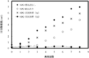
- Example 2 Verification of effect due to difference in initial oxygen concentration between nitrogen-doped wafer and NPC wafer Diameter 200 mm, nitrogen concentration 5 ⁇ 10 13 atoms / cm 3 , initial oxygen concentration 3 to 17 ppma wafer, diameter 200 mm, N region (NPC), initial A wafer having an oxygen concentration of 3 to 17 ppma was subjected to a heat treatment at 1200 ° C. for 60 minutes in an oxygen atmosphere, and then the pseudo regeneration method was repeated five times in the same manner as in Example 1 to measure the HF defect density. The results are shown in FIG.
- Example 3 Manufacturing of SOI wafers 1
- a bond wafer a mirror-polished silicon wafer having a diameter of 200 mm, an N region (NPC), and an initial oxygen concentration of 12 ppma was prepared, and heat treatment for eliminating defects of the bond wafer was performed at 1200 ° C. for 60 minutes in an oxygen atmosphere. Then, after removing the oxide film by etching with HF, the surface to be the bonded surface was polished by 0.1 ⁇ m. Then, (i) after performing an oxidation heat treatment at 900 ° C./6 hrs to form an oxide film, (ii) hydrogen ions are implanted through this oxide film (implantation conditions are acceleration energy 70 keV, implantation amount 6 ⁇ 10 16 / cm 2.
- the obtained SOI wafer was a high-quality one having no defects such as defects in the SOI layer and excellent electrical characteristics.
- Example 4 Manufacturing of SOI wafers 2 An SOI wafer was prepared in the same manner as in Example 3 except that a bonded wafer was prepared as a mirror-polished silicon wafer having a diameter of 200 mm, nitrogen dope (nitrogen concentration 5 ⁇ 10 13 atoms / cm 3 ), and initial oxygen concentration 6 ppma. Produced.
- the HF defect was at a level with no problem.
- the obtained SOI wafer was a high-quality one having no defects such as defects in the SOI layer and excellent electrical characteristics.
- the present invention is not limited to the above embodiment.
- the above-described embodiment is an exemplification, and the present invention has any configuration that has substantially the same configuration as the technical idea described in the claims of the present invention and that exhibits the same effects. Are included in the technical scope.
Landscapes
- Engineering & Computer Science (AREA)
- Physics & Mathematics (AREA)
- Condensed Matter Physics & Semiconductors (AREA)
- General Physics & Mathematics (AREA)
- Manufacturing & Machinery (AREA)
- Computer Hardware Design (AREA)
- Microelectronics & Electronic Packaging (AREA)
- Power Engineering (AREA)
- Chemical & Material Sciences (AREA)
- Materials Engineering (AREA)
- Crystallography & Structural Chemistry (AREA)
- Metallurgy (AREA)
- Organic Chemistry (AREA)
- Electromagnetism (AREA)
- Element Separation (AREA)
- High Energy & Nuclear Physics (AREA)
- Health & Medical Sciences (AREA)
- Toxicology (AREA)
- Mechanical Treatment Of Semiconductor (AREA)
- Crystals, And After-Treatments Of Crystals (AREA)
Priority Applications (5)
| Application Number | Priority Date | Filing Date | Title |
|---|---|---|---|
| SG11201501678UA SG11201501678UA (en) | 2012-10-16 | 2013-09-12 | Method of manufacturing soi wafer |
| EP13846328.6A EP2911183A1 (en) | 2012-10-16 | 2013-09-12 | Soi wafer manufacturing method |
| CN201380047651.XA CN104620351A (zh) | 2012-10-16 | 2013-09-12 | Soi晶圆的制造方法 |
| US14/426,582 US20150287630A1 (en) | 2012-10-16 | 2013-09-12 | Method of manufacturing soi wafer |
| KR1020157005883A KR20150070096A (ko) | 2012-10-16 | 2013-09-12 | Soi 웨이퍼의 제조방법 |
Applications Claiming Priority (2)
| Application Number | Priority Date | Filing Date | Title |
|---|---|---|---|
| JP2012-229111 | 2012-10-16 | ||
| JP2012229111A JP2014082316A (ja) | 2012-10-16 | 2012-10-16 | Soiウェーハの製造方法 |
Publications (1)
| Publication Number | Publication Date |
|---|---|
| WO2014061196A1 true WO2014061196A1 (ja) | 2014-04-24 |
Family
ID=50487777
Family Applications (1)
| Application Number | Title | Priority Date | Filing Date |
|---|---|---|---|
| PCT/JP2013/005396 WO2014061196A1 (ja) | 2012-10-16 | 2013-09-12 | Soiウェーハの製造方法 |
Country Status (7)
Families Citing this family (4)
| Publication number | Priority date | Publication date | Assignee | Title |
|---|---|---|---|---|
| JP7172747B2 (ja) * | 2019-03-06 | 2022-11-16 | 信越半導体株式会社 | シリコン単結晶の抵抗率測定方法 |
| TWI845675B (zh) * | 2019-05-23 | 2024-06-21 | 日商東京威力科創股份有限公司 | 基板處理方法及基板處理系統 |
| US12164126B2 (en) * | 2021-06-30 | 2024-12-10 | Openlight Photonics, Inc. | High bandwidth photonic integrated circuit with etalon compensation |
| CN113655094B (zh) * | 2021-08-06 | 2024-01-19 | 上海新昇半导体科技有限公司 | 一种确定硅片导电类型的方法 |
Citations (7)
| Publication number | Priority date | Publication date | Assignee | Title |
|---|---|---|---|---|
| WO2004073057A1 (ja) * | 2003-02-14 | 2004-08-26 | Sumitomo Mitsubishi Silicon Corporation | シリコンウェーハの製造方法 |
| JP2006294737A (ja) | 2005-04-07 | 2006-10-26 | Sumco Corp | Soi基板の製造方法及びその製造における剥離ウェーハの再生処理方法。 |
| JP2007149907A (ja) | 2005-11-28 | 2007-06-14 | Sumco Corp | 剥離ウェーハの再生加工方法及びこの方法により再生加工された剥離ウェーハ |
| JP2008021892A (ja) | 2006-07-14 | 2008-01-31 | Shin Etsu Handotai Co Ltd | 剥離ウェーハを再利用する方法 |
| JP2011176293A (ja) | 2010-01-26 | 2011-09-08 | Semiconductor Energy Lab Co Ltd | Soi基板の作製方法 |
| JP2011238758A (ja) | 2010-05-10 | 2011-11-24 | Shin Etsu Handotai Co Ltd | Soiウェーハの製造方法 |
| JP2012153548A (ja) * | 2011-01-24 | 2012-08-16 | Shin Etsu Handotai Co Ltd | シリコン単結晶ウェーハの製造方法及びアニールウェーハ |
-
2012
- 2012-10-16 JP JP2012229111A patent/JP2014082316A/ja active Pending
-
2013
- 2013-09-12 EP EP13846328.6A patent/EP2911183A1/en not_active Withdrawn
- 2013-09-12 KR KR1020157005883A patent/KR20150070096A/ko not_active Withdrawn
- 2013-09-12 WO PCT/JP2013/005396 patent/WO2014061196A1/ja active Application Filing
- 2013-09-12 SG SG11201501678UA patent/SG11201501678UA/en unknown
- 2013-09-12 US US14/426,582 patent/US20150287630A1/en not_active Abandoned
- 2013-09-12 CN CN201380047651.XA patent/CN104620351A/zh active Pending
Patent Citations (7)
| Publication number | Priority date | Publication date | Assignee | Title |
|---|---|---|---|---|
| WO2004073057A1 (ja) * | 2003-02-14 | 2004-08-26 | Sumitomo Mitsubishi Silicon Corporation | シリコンウェーハの製造方法 |
| JP2006294737A (ja) | 2005-04-07 | 2006-10-26 | Sumco Corp | Soi基板の製造方法及びその製造における剥離ウェーハの再生処理方法。 |
| JP2007149907A (ja) | 2005-11-28 | 2007-06-14 | Sumco Corp | 剥離ウェーハの再生加工方法及びこの方法により再生加工された剥離ウェーハ |
| JP2008021892A (ja) | 2006-07-14 | 2008-01-31 | Shin Etsu Handotai Co Ltd | 剥離ウェーハを再利用する方法 |
| JP2011176293A (ja) | 2010-01-26 | 2011-09-08 | Semiconductor Energy Lab Co Ltd | Soi基板の作製方法 |
| JP2011238758A (ja) | 2010-05-10 | 2011-11-24 | Shin Etsu Handotai Co Ltd | Soiウェーハの製造方法 |
| JP2012153548A (ja) * | 2011-01-24 | 2012-08-16 | Shin Etsu Handotai Co Ltd | シリコン単結晶ウェーハの製造方法及びアニールウェーハ |
Also Published As
| Publication number | Publication date |
|---|---|
| US20150287630A1 (en) | 2015-10-08 |
| CN104620351A (zh) | 2015-05-13 |
| EP2911183A1 (en) | 2015-08-26 |
| KR20150070096A (ko) | 2015-06-24 |
| SG11201501678UA (en) | 2015-04-29 |
| JP2014082316A (ja) | 2014-05-08 |
Similar Documents
| Publication | Publication Date | Title |
|---|---|---|
| JP4715470B2 (ja) | 剥離ウェーハの再生加工方法及びこの方法により再生加工された剥離ウェーハ | |
| EP2048697B1 (en) | Method for reusing delaminated wafer | |
| CN105190835B (zh) | 混合基板的制造方法和混合基板 | |
| JP2006216826A (ja) | Soiウェーハの製造方法 | |
| WO2013102968A1 (ja) | 貼り合わせsoiウェーハの製造方法 | |
| JP4419147B2 (ja) | 貼り合わせウェーハの製造方法 | |
| KR101910100B1 (ko) | Soi 웨이퍼의 제조방법 | |
| JP2014120587A (ja) | Soiウェーハの製造方法 | |
| JP6056516B2 (ja) | Soiウェーハの製造方法及びsoiウェーハ | |
| WO2014061196A1 (ja) | Soiウェーハの製造方法 | |
| JP2008016534A (ja) | 貼り合わせウェーハの製造方法 | |
| JP5522175B2 (ja) | Soiウェーハの製造方法 | |
| JP2011515838A (ja) | セミコンダクタオンインシュレータ型基板を製作する方法 | |
| US20190198386A1 (en) | Method for manufacturing bonded soi wafer | |
| WO2014080565A1 (ja) | Soiウェーハの製造方法 | |
| JP2010098167A (ja) | 貼り合わせウェーハの製造方法 | |
| JP5541136B2 (ja) | 貼り合わせsoiウエーハの製造方法 | |
| JP5125194B2 (ja) | 貼り合わせウエーハの製造方法 | |
| WO2016059748A1 (ja) | 貼り合わせウェーハの製造方法 | |
| WO2017217129A1 (ja) | 貼り合わせウェーハの製造方法 | |
| KR102317552B1 (ko) | 접합 soi 웨이퍼의 제조방법 | |
| JP5211550B2 (ja) | シリコン単結晶ウェーハの製造方法 | |
| JP2652346B2 (ja) | シリコンウエーハの製造方法 |
Legal Events
| Date | Code | Title | Description |
|---|---|---|---|
| 121 | Ep: the epo has been informed by wipo that ep was designated in this application |
Ref document number: 13846328 Country of ref document: EP Kind code of ref document: A1 |
|
| ENP | Entry into the national phase |
Ref document number: 20157005883 Country of ref document: KR Kind code of ref document: A |
|
| WWE | Wipo information: entry into national phase |
Ref document number: 14426582 Country of ref document: US Ref document number: 2013846328 Country of ref document: EP |
|
| NENP | Non-entry into the national phase |
Ref country code: DE |