WO2014050322A1 - チップ部品およびその製造方法 - Google Patents
チップ部品およびその製造方法 Download PDFInfo
- Publication number
- WO2014050322A1 WO2014050322A1 PCT/JP2013/071412 JP2013071412W WO2014050322A1 WO 2014050322 A1 WO2014050322 A1 WO 2014050322A1 JP 2013071412 W JP2013071412 W JP 2013071412W WO 2014050322 A1 WO2014050322 A1 WO 2014050322A1
- Authority
- WO
- WIPO (PCT)
- Prior art keywords
- substrate
- film
- chip
- electrode
- resistor
- Prior art date
- Legal status (The legal status is an assumption and is not a legal conclusion. Google has not performed a legal analysis and makes no representation as to the accuracy of the status listed.)
- Ceased
Links
Images











Classifications
-
- H—ELECTRICITY
- H01—ELECTRIC ELEMENTS
- H01C—RESISTORS
- H01C1/00—Details
- H01C1/01—Mounting; Supporting
- H01C1/012—Mounting; Supporting the base extending along and imparting rigidity or reinforcement to the resistive element
-
- H—ELECTRICITY
- H01—ELECTRIC ELEMENTS
- H01C—RESISTORS
- H01C1/00—Details
- H01C1/14—Terminals or tapping points specially adapted for resistors; Arrangements of terminals or tapping points on resistors
-
- H—ELECTRICITY
- H01—ELECTRIC ELEMENTS
- H01C—RESISTORS
- H01C1/00—Details
- H01C1/16—Resistor networks not otherwise provided for
-
- H—ELECTRICITY
- H01—ELECTRIC ELEMENTS
- H01G—CAPACITORS; CAPACITORS, RECTIFIERS, DETECTORS, SWITCHING DEVICES, LIGHT-SENSITIVE OR TEMPERATURE-SENSITIVE DEVICES OF THE ELECTROLYTIC TYPE
- H01G2/00—Details of capacitors not covered by a single one of groups H01G4/00-H01G11/00
- H01G2/02—Mountings
- H01G2/06—Mountings specially adapted for mounting on a printed-circuit support
- H01G2/065—Mountings specially adapted for mounting on a printed-circuit support for surface mounting, e.g. chip capacitors
-
- H—ELECTRICITY
- H01—ELECTRIC ELEMENTS
- H01G—CAPACITORS; CAPACITORS, RECTIFIERS, DETECTORS, SWITCHING DEVICES, LIGHT-SENSITIVE OR TEMPERATURE-SENSITIVE DEVICES OF THE ELECTROLYTIC TYPE
- H01G4/00—Fixed capacitors; Processes of their manufacture
- H01G4/002—Details
- H01G4/005—Electrodes
- H01G4/012—Form of non-self-supporting electrodes
-
- H—ELECTRICITY
- H01—ELECTRIC ELEMENTS
- H01G—CAPACITORS; CAPACITORS, RECTIFIERS, DETECTORS, SWITCHING DEVICES, LIGHT-SENSITIVE OR TEMPERATURE-SENSITIVE DEVICES OF THE ELECTROLYTIC TYPE
- H01G4/00—Fixed capacitors; Processes of their manufacture
- H01G4/002—Details
- H01G4/228—Terminals
-
- H—ELECTRICITY
- H01—ELECTRIC ELEMENTS
- H01G—CAPACITORS; CAPACITORS, RECTIFIERS, DETECTORS, SWITCHING DEVICES, LIGHT-SENSITIVE OR TEMPERATURE-SENSITIVE DEVICES OF THE ELECTROLYTIC TYPE
- H01G4/00—Fixed capacitors; Processes of their manufacture
- H01G4/40—Structural combinations of fixed capacitors with other electric elements, the structure mainly consisting of a capacitor, e.g. RC combinations
-
- H—ELECTRICITY
- H01—ELECTRIC ELEMENTS
- H01G—CAPACITORS; CAPACITORS, RECTIFIERS, DETECTORS, SWITCHING DEVICES, LIGHT-SENSITIVE OR TEMPERATURE-SENSITIVE DEVICES OF THE ELECTROLYTIC TYPE
- H01G5/00—Capacitors in which the capacitance is varied by mechanical means, e.g. by turning a shaft; Processes of their manufacture
- H01G5/01—Details
-
- H—ELECTRICITY
- H05—ELECTRIC TECHNIQUES NOT OTHERWISE PROVIDED FOR
- H05K—PRINTED CIRCUITS; CASINGS OR CONSTRUCTIONAL DETAILS OF ELECTRIC APPARATUS; MANUFACTURE OF ASSEMBLAGES OF ELECTRICAL COMPONENTS
- H05K1/00—Printed circuits
- H05K1/18—Printed circuits structurally associated with non-printed electric components
- H05K1/181—Printed circuits structurally associated with non-printed electric components associated with surface mounted components
-
- H—ELECTRICITY
- H01—ELECTRIC ELEMENTS
- H01C—RESISTORS
- H01C17/00—Apparatus or processes specially adapted for manufacturing resistors
- H01C17/06—Apparatus or processes specially adapted for manufacturing resistors adapted for coating resistive material on a base
-
- H—ELECTRICITY
- H01—ELECTRIC ELEMENTS
- H01C—RESISTORS
- H01C7/00—Non-adjustable resistors formed as one or more layers or coatings; Non-adjustable resistors made from powdered conducting material or powdered semi-conducting material with or without insulating material
- H01C7/003—Thick film resistors
-
- H—ELECTRICITY
- H01—ELECTRIC ELEMENTS
- H01G—CAPACITORS; CAPACITORS, RECTIFIERS, DETECTORS, SWITCHING DEVICES, LIGHT-SENSITIVE OR TEMPERATURE-SENSITIVE DEVICES OF THE ELECTROLYTIC TYPE
- H01G4/00—Fixed capacitors; Processes of their manufacture
- H01G4/002—Details
- H01G4/005—Electrodes
- H01G4/008—Selection of materials
-
- H—ELECTRICITY
- H01—ELECTRIC ELEMENTS
- H01G—CAPACITORS; CAPACITORS, RECTIFIERS, DETECTORS, SWITCHING DEVICES, LIGHT-SENSITIVE OR TEMPERATURE-SENSITIVE DEVICES OF THE ELECTROLYTIC TYPE
- H01G4/00—Fixed capacitors; Processes of their manufacture
- H01G4/30—Stacked capacitors
Definitions
- Patent Document 1 discloses a chip resistor in which a resistive film formed on an insulating substrate is laser trimmed and then a glass cover coat is formed.
- the electrodes are formed only on one side of the insulating substrate. For this reason, when this chip resistor is soldered to the mounting substrate, the chip resistor is bonded to the mounting substrate only on the one surface, and thus the bonding strength may not be sufficient. Moreover, since the bonding surface is only one surface, the chip resistor is not stabilized on the solder, and when a lateral force along the bonding surface (direction along the mounting substrate) is applied to the chip resistor. In addition, there is a problem that the chip resistor is easily detached.
- Another object of the present invention is to provide a chip component manufacturing method that can easily manufacture a chip component that can improve the adhesive strength with the mounting substrate and can further stabilize the mounting shape. It is.
- the electrode is not simply formed on the side surface of the substrate, but an insulating film is interposed between the electrode and the substrate. Thereby, for example, when it is not desired to short-circuit the substrate and the electrode, the requirement can be met.
- the substrate has a rectangular shape in a plan view, and the electrodes are formed so as to cover the edge portions on three sides of the substrate.
- the chip component can be held from the three directions of the side surface of the substrate in the mounted state, so that the mounted shape of the chip component can be further stabilized.
- the electrode may be formed so as to protrude from the surface of the resin film. In that case, it may include a drawer portion that is pulled out in the lateral direction along the surface of the resin film and selectively covers the surface.
- the electrode preferably includes a Ni layer and an Au layer, and the Au layer is exposed on the outermost surface.
- the Ni layer can be prevented from being oxidized.
- the electrode further includes a Pd layer interposed between the Ni layer and the Au layer.
- the Pd layer interposed between the Ni layer and the Au layer blocks the through hole. Therefore, the Ni layer can be prevented from being exposed to the outside through the through hole and being oxidized.
- the chip component may be a chip resistor including a resistor formed on the substrate and connected between the two electrodes when the two electrodes are provided with a space therebetween.
- the chip component further includes a plurality of resistors and a plurality of fuses provided on the substrate and connected to the electrodes so as to be detachable from each other.
- this chip component chip resistor
- by selecting and cutting one or a plurality of fuses it is possible to easily and quickly cope with a plurality of types of resistance values.
- chip resistors having various resistance values can be realized with a common design by combining a plurality of resistors having different resistance values.
- the chip component may be a chip capacitor including a capacitor element formed on the substrate and connected between the two electrodes when the two electrodes are provided with a space therebetween. .
- the chip component further includes a plurality of capacitor elements constituting the capacitor element, and a plurality of fuses provided on the substrate and detachably connected to the electrodes. Is preferred.
- this chip component chip capacitor
- by selecting and cutting one or a plurality of fuses it is possible to easily and quickly cope with a plurality of types of capacitance values.
- chip capacitors having various capacitance values can be realized by a common design by combining a plurality of capacitor elements having different capacitance values.
- the circuit assembly of the present invention includes the chip component of the present invention and a mounting substrate having lands soldered to the electrodes on a mounting surface facing the surface of the substrate. With this configuration, it is possible to provide a circuit assembly including a chip component that can improve the adhesive strength with the mounting substrate and further stabilize the mounting shape.
- the circuit assembly is preferably formed so that the solder covers the surface portion and the side surface portion of the electrode when viewed from the normal direction of the mounting surface.
- the amount of solder adsorbed to the electrode can be increased, and the adhesive strength can be improved.
- the chip component can be held from the two directions of the surface and side surface of the substrate. Therefore, the mounting shape of the chip component can be stabilized.
- the electronic device of the present invention includes the circuit assembly of the present invention and a housing that houses the circuit assembly. With this configuration, it is possible to provide an electronic component including a chip component that can improve the adhesive strength with the mounting substrate and further stabilize the mounting shape.
- the chip component manufacturing method of the present invention includes a step of forming a groove having a predetermined depth from the surface of the substrate in a boundary region between the plurality of chip component regions of the substrate, and separating the substrate into the plurality of chip component regions.
- the chip component of the present invention can be easily manufactured by plating growth of the electrode material.
- the step of forming the electrode preferably includes a step of growing the electrode material by electroless plating.
- the electrode material can be grown well on the insulating film.
- productivity can be improved by reducing the number of processes compared to electrolytic plating.
- the groove is preferably formed by etching. In this method, since grooves can be formed at a time in the boundary region of all chip component regions on the substrate, the time required for manufacturing the chip components can be reduced.
- FIG. 1A is a schematic perspective view for explaining a configuration of a chip resistor according to an embodiment of the present invention.
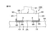
- FIG. 1B is a schematic cross-sectional view of the circuit assembly in a state where the chip resistor is mounted on the mounting substrate, cut along the longitudinal direction of the chip resistor.
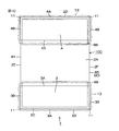
- FIG. 1C is a schematic plan view of the chip resistor mounted on the mounting substrate as viewed from the element forming surface side.
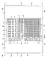
- FIG. 2 is a plan view of the chip resistor, showing the arrangement relationship of the first connection electrode, the second connection electrode and the element, and the configuration of the element in plan view.
- FIG. 3A is a plan view illustrating a part of the element shown in FIG. 2 in an enlarged manner.
- FIG. 3A is a plan view illustrating a part of the element shown in FIG. 2 in an enlarged manner.
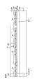
- FIG. 3B is a longitudinal sectional view in the length direction taken along the line BB in FIG. 3A for explaining the configuration of the resistor in the element.
- FIG. 3C is a longitudinal sectional view in the width direction along CC of FIG. 3A drawn to explain the configuration of the resistor in the element.
- FIG. 4 is a diagram showing the electrical characteristics of the resistor film line and the wiring film with circuit symbols and electrical circuit diagrams.
- FIG. 5A is a partially enlarged plan view of a region including a fuse drawn by enlarging a part of the plan view of the chip resistor of FIG. 2, and
- FIG. 5B is a view of B in FIG. It is a figure which shows the cross-sectional structure which follows -B.
- FIG. 5A is a partially enlarged plan view of a region including a fuse drawn by enlarging a part of the plan view of the chip resistor of FIG. 2
- FIG. 5B is a view of B in FIG. It is a figure which
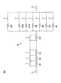
- FIG. 6 is an electric circuit diagram of the element according to the embodiment of the present invention.
- FIG. 7 is an electric circuit diagram of an element according to another embodiment of the present invention.
- FIG. 8 is an electric circuit diagram of an element according to still another embodiment of the present invention.
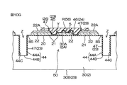
- FIG. 9 is a schematic cross-sectional view of a chip resistor.
- FIG. 10A is a cross-sectional view illustrating a method of manufacturing the chip resistor of FIG.
- FIG. 10B is a cross-sectional view showing a step subsequent to FIG. 10A.
- FIG. 10C is a cross-sectional view showing a step subsequent to FIG. 10B.
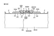
- FIG. 10D is a cross-sectional view showing a step subsequent to FIG. 10C.
- FIG. 10A is a cross-sectional view illustrating a method of manufacturing the chip resistor of FIG.
- FIG. 10B is a cross-sectional view showing a step subsequent to FIG. 10A.
- FIG. 10C is a cross-section
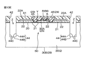
- FIG. 10E is a cross-sectional view showing a step subsequent to FIG. 10D.
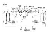
- FIG. 10F is a cross-sectional view showing a step subsequent to FIG. 10E.
- FIG. 10G is a cross-sectional view showing a step subsequent to FIG. 10F.
- FIG. 10H is a cross-sectional view showing a step subsequent to FIG. 10G.
- FIG. 10I is a cross-sectional view showing a step subsequent to FIG. 10H.
- FIG. 11 is a schematic plan view of a part of a resist pattern used for forming a groove in the step of FIG. 10E.
- FIG. 12 is a diagram for explaining a manufacturing process of the first connection electrode and the second connection electrode.
- FIG. 15 is a plan view of a chip capacitor according to another embodiment of the present invention.
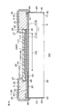
- 16 is a cross-sectional view taken along section line XVI-XVI in FIG.
- FIG. 17 is an exploded perspective view showing a part of the structure of the chip capacitor separately.
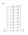
- FIG. 18 is a circuit diagram showing an internal electrical configuration of the chip capacitor.
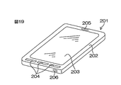
- FIG. 19 is a perspective view showing an appearance of a smartphone which is an example of an electronic device in which the chip component of the present invention is used.
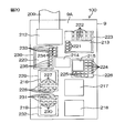
- FIG. 20 is a schematic plan view showing the configuration of the circuit assembly housed in the housing of the smartphone.
- the chip resistor 1 is a minute chip part and has a rectangular parallelepiped shape as shown in FIG. 1A.
- the planar shape of the chip resistor 1 is a rectangle having two orthogonal sides (long side 81 and short side 82) of 0.4 mm or less and 0.2 mm or less, respectively.
- the length L (length of the long side 81) is about 0.3 mm
- the width W (length of the short side 82) is about 0.15 mm
- the thickness T is about 0.1 mm.
- the chip resistor 1 is formed by forming a plurality of chip resistors 1 in a lattice shape on a substrate, forming grooves in the substrate, and then polishing the back surface (or dividing the substrate by the grooves) to obtain individual chips. It is obtained by separating the resistor 1.
- the chip resistor 1 is externally provided by a substrate 2 constituting the main body of the chip resistor 1, a first connection electrode 3 and a second connection electrode 4 that are external connection electrodes, and a first connection electrode 3 and a second connection electrode 4. It mainly includes an element 5 to be connected.
- the substrate 2 has a substantially rectangular parallelepiped chip shape.
- One surface forming the upper surface in FIG. 1A of the substrate 2 is an element formation surface 2A.
- the element formation surface 2A is a surface on which the element 5 is formed on the substrate 2 and has a substantially rectangular shape.
- the surface opposite to the element formation surface 2A in the thickness direction of the substrate 2 is a back surface 2B.
- the element formation surface 2A and the back surface 2B have substantially the same size and shape, and are parallel to each other.
- the rectangular edge defined by the pair of long sides 81 and short sides 82 on the element forming surface 2A is referred to as a peripheral edge 85, and the rectangular shape defined by the pair of long sides 81 and short sides 82 on the back surface 2B.
- the edge is referred to as the peripheral edge 90.
- the peripheral edge portion 85 and the peripheral edge portion 90 overlap each other (see FIG. 1C described later).
- the substrate 2 has a plurality of side surfaces (side surface 2C, side surface 2D, side surface 2E, and side surface 2F) as surfaces other than the element formation surface 2A and the back surface 2B.
- the plurality of side surfaces extend so as to intersect (specifically, orthogonally cross) each of the element formation surface 2A and the back surface 2B, and connect the element formation surface 2A and the back surface 2B.
- the side surface 2E and the side surface 2F are both end surfaces of the substrate 2 in the lateral direction.
- Each of the side surface 2C and the side surface 2D intersects (specifically, orthogonal) with each of the side surface 2E and the side surface 2F. Therefore, adjacent elements forming surface 2A to side surface 2F form a right angle.
- the chip resistor 1 has a resin film 24.
- the resin film 24 covers the entire region of the passivation film 23 on the element formation surface 2A (peripheral portion 85 and its inner region). The passivation film 23 and the resin film 24 will be described in detail later.
- the first connection electrode 3 and the second connection electrode 4 are integrally formed so as to straddle the element formation surface 2A and the side surfaces 2C to 2F so as to cover the peripheral edge 85 on the element formation surface 2A of the substrate 2. .
- Each of the first connection electrode 3 and the second connection electrode 4 is configured, for example, by stacking Ni (nickel), Pd (palladium), and Au (gold) on the element formation surface 2A in this order.
- the first connection electrode 3 and the second connection electrode 4 are arranged at a distance from each other in the longitudinal direction of the element formation surface 2A.
- the first connection electrode 3 has three side surfaces 2C, 2E, and 2F along one short side 82 (short side 82 near the side surface 2C) of the chip resistor 1 and a pair of long sides 81 on both sides thereof. Are integrally covered.
- the second connection electrode 4 is formed by integrating the other short side 82 (short side 82 near the side surface 2D) of the chip resistor 1 and the three side surfaces 2D, 2E, 2F along the pair of long sides 81 on both sides thereof. It is formed so as to cover. Thereby, each corner part 11 in which side surfaces cross in the longitudinal direction both ends of the board
- the first connection electrode 3 and the second connection electrode 4 have substantially the same size and the same shape in a plan view viewed from the normal direction described above.
- the first connection electrode 3 has a pair of long sides 3A and short sides 3B that form four sides in a plan view.
- the long side 3A and the short side 3B are orthogonal to each other in plan view.
- the second connection electrode 4 has a pair of long sides 4A and short sides 4B that form four sides in plan view.
- the long side 4A and the short side 4B are orthogonal to each other in plan view.
- the long side 3A and the long side 4A extend in parallel with the short side 82 of the substrate 2, and the short side 3B and the short side 4B extend in parallel with the long side 81 of the substrate 2.
- the chip resistor 1 does not have an electrode on the back surface 2B.
- the element 5 is a circuit element, and is formed in a region between the first connection electrode 3 and the second connection electrode 4 on the element formation surface 2A of the substrate 2, and from above by the passivation film 23 and the resin film 24. It is covered.
- the element 5 of this embodiment is a resistor 56.
- the resistor 56 is constituted by a circuit network in which a plurality of (unit) resistors R having equal resistance values are arranged in a matrix on the element formation surface 2A.
- the resistor R is made of TiN (titanium nitride), TiON (titanium oxynitride) or TiSiON.
- FIG. 1B is a schematic cross-sectional view of the circuit assembly in a state where the chip resistor is mounted on the mounting substrate, cut along the longitudinal direction of the chip resistor. In addition, in FIG. 1B, only the principal part is shown with the cross section.
- the chip resistor 1 When the chip resistor 1 is mounted on the mounting substrate 9, the chip resistor 1 is moved by moving the suction nozzle 91 after the suction nozzle 91 of the automatic mounting machine (not shown) is attracted to the back surface 2B of the chip resistor 1. Transport. At this time, the suction nozzle 91 is sucked to a substantially central portion in the longitudinal direction of the back surface 2B.
- the first connection electrode 3 and the second connection electrode 4 are provided only on one side (element formation surface 2A) of the chip resistor 1 and the end portion on the element formation surface 2A side of the side surfaces 2C to 2F. For this reason, the back surface 2B of the chip resistor 1 is a flat surface without electrodes (unevenness).
- the suction nozzle 91 when the suction nozzle 91 is attracted to the chip resistor 1 and moved, the suction nozzle 91 can be attracted to the flat back surface 2B. In other words, if the back surface 2B is flat, the margin of the portion that can be sucked by the suction nozzle 91 can be increased. Thus, the suction nozzle 91 can be reliably attracted to the chip resistor 1, and the chip resistor 1 can be reliably transported without dropping from the suction nozzle 91 in the middle.
- the suction nozzle 91 that sucks the chip resistor 1 is moved to the mounting substrate 9.
- the element formation surface 2A of the chip resistor 1 and the mounting surface 9A of the mounting substrate 9 face each other.
- the suction nozzle 91 is moved and pressed against the mounting substrate 9.
- the first connection electrode 3 is brought into contact with the solder 13 of one land 88
- the second connection electrode 4 is brought into contact with the other land 88.
- the solder 13 is contacted.
- the solder 13 is heated, the solder 13 is melted.
- first connection electrode 3 and the one land 88 are joined via the solder 13, and the second connection electrode 4 and the other land 88 are joined via the solder 13.
- each of the two lands 88 is soldered to the corresponding electrode in the first connection electrode 3 and the second connection electrode 4.
- mounting of the chip resistor 1 on the mounting substrate 9 flip chip connection
- the circuit assembly 100 is completed.
- the first connection electrode 3 and the second connection electrode 4 that function as external connection electrodes are formed of gold (Au) in order to improve solder wettability and reliability, or as described later. It is desirable to apply gold plating to the surface.
- the element formation surface 2A of the chip resistor 1 and the mounting surface 9A of the mounting substrate 9 extend in parallel while facing each other with a gap (see also FIG. 1C).
- the dimension of the gap corresponds to the sum of the thickness of the portion protruding from the element formation surface 2 ⁇ / b> A in the first connection electrode 3 or the second connection electrode 4 and the thickness of the solder 13.
- FIG. 1C is a schematic plan view of the chip resistor mounted on the mounting substrate as seen from the element forming surface side. Next, the mounting shape of the chip resistor 1 will be described with reference to FIGS. 1B and 1C.
- the first connection electrode 3 and the second connection electrode 4 are formed such that the surface portion on the element formation surface 2A and the side portions on the side surfaces 2C and 2D are integrated. And is formed in an L shape. Therefore, as shown in FIG. 1C, the circuit assembly 100 (strictly speaking, the chip resistor 1 and the mounting substrate 9 are separated from the normal direction of the mounting surface 9A (element forming surface 2A) (the direction orthogonal to these surfaces). Looking at the joint portion), the solder 13 joining the first connection electrode 3 and one land 88 is adsorbed not only on the surface portion of the first connection electrode 3 but also on the side surface portion. Similarly, the solder 13 joining the second connection electrode 4 and the other land 88 is adsorbed not only on the surface portion of the second connection electrode 4 but also on the side surface portion.
- the solder 13 is adsorbed so as to go around from the element forming surface 2A of the substrate 2 to the side surfaces 2C to 2F. Accordingly, in the mounted state, the first connection electrode 3 is held by the solder 13 on the three side surfaces 2C, 2E, 2F, and the second connection electrode 4 is held by the solder 13 on the three side surfaces 2D, 2E, 2F. All the side surfaces 2C to 2F of the shaped chip resistor 1 can be fixed by the solder 13. Thereby, the mounting shape of the chip resistor 1 can be stabilized.
- FIG. 2 is a plan view of the chip resistor, showing the arrangement relationship between the first connection electrode, the second connection electrode and the element, and the configuration (layout pattern) of the element in plan view.
- element 5 is a resistance network. Specifically, the element 5 includes eight resistors R arranged along the row direction (longitudinal direction of the substrate 2) and 44 resistors arranged along the column direction (width direction of the substrate 2). It has a total of 352 resistors R composed of the body R. These resistors R are a plurality of element elements constituting a resistance network of the element 5.
- a plurality of types of resistor circuits R are formed by grouping and electrically connecting a large number of these resistors R every predetermined number of 1 to 64.
- the formed plurality of types of resistance circuits are connected in a predetermined manner by a conductor film D (a wiring film formed of a conductor).
- a plurality of fuses F that can be cut (blown) in order to electrically incorporate a resistance circuit with respect to the element 5 or to electrically separate it from the element 5 are formed on the element forming surface 2A of the substrate 2. Is provided.
- the plurality of fuses F and the conductor film D are arranged along the inner side of the first connection electrode 3 so that the arrangement region is linear.
- the plurality of fuses F and the conductor film D are arranged so as to be adjacent to each other, and the arrangement direction thereof is linear.
- the plurality of fuses F connect a plurality of types of resistor circuits (a plurality of resistors R for each resistor circuit) to the first connection electrode 3 so as to be cut (separable).
- FIG. 3A is a plan view illustrating a part of the element shown in FIG. 2 in an enlarged manner.
- FIG. 3B is a longitudinal sectional view in the length direction taken along the line BB in FIG. 3A for explaining the configuration of the resistor in the element.
- FIG. 3C is a longitudinal sectional view in the width direction along CC of FIG. 3A drawn to explain the configuration of the resistor in the element.
- resistor R The structure of the resistor R will be described with reference to FIGS. 3A, 3B, and 3C.
- the chip resistor 1 further includes an insulating film 20 and a resistor film 21 in addition to the wiring film 22, the passivation film 23, and the resin film 24 described above (see FIGS. 3B and 3C).
- the insulating film 20, the resistor film 21, the wiring film 22, the passivation film 23, and the resin film 24 are formed on the substrate 2 (element formation surface 2A).
- the insulating film 20 is made of SiO 2 (silicon oxide).
- the insulating film 20 covers the entire area of the element formation surface 2 ⁇ / b> A of the substrate 2.
- the insulating film 20 has a thickness of about 10,000 mm.
- the resistor film 21 is formed on the insulating film 20.
- the resistor film 21 is made of TiN, TiON, or TiSiON.
- the thickness of the resistor film 21 is about 2000 mm.
- the resistor film 21 constitutes a plurality of resistor films (hereinafter referred to as “resistor film line 21 ⁇ / b> A”) extending linearly in parallel between the first connection electrode 3 and the second connection electrode 4.
- the resistor film line 21A may be cut at a predetermined position in the line direction (see FIG. 3A).
- the wiring film 22 is laminated on the resistor film line 21A.
- the wiring film 22 is made of Al (aluminum) or an alloy of aluminum and Cu (copper) (AlCu alloy).
- the thickness of the wiring film 22 is about 8000 mm.
- the wiring film 22 is laminated on the resistor film line 21A at a predetermined interval R in the line direction, and is in contact with the resistor film line 21A.
- FIG. 4 shows the electrical characteristics of the resistor film line 21A and the wiring film 22 of this configuration by circuit symbols. That is, as shown in FIG. 4A, each of the resistor film lines 21A in the region of the predetermined interval R forms one resistor R having a certain resistance value r.
- each resistor R includes a resistor film line 21A (resistor film 21) and a plurality of wiring films 22 stacked on the resistor film line 21A at a predetermined interval in the line direction.
- a resistor film line 21A at a constant interval R where 22 is not laminated constitutes one resistor R.
- the resistor film lines 21A in the portion constituting the resistor R are all equal in shape and size. Therefore, the multiple resistors R arranged in a matrix on the substrate 2 have equal resistance values.
- the wiring film 22 laminated on the resistor film line 21A forms the resistor R and also plays a role of the conductor film D for connecting a plurality of resistors R to form a resistor circuit. (See FIG. 2).
- FIG. 5A is a partial enlarged plan view of a region including a fuse drawn by enlarging a part of the plan view of the chip resistor shown in FIG. 2, and FIG. 5B is a plan view of FIG. It is a figure which shows the cross-sectional structure which follows BB.
- the above-described fuse F and conductor film D are also formed by the wiring film 22 laminated on the resistor film 21 forming the resistor R. That is, the fuse F and the conductor film D are formed on the same layer as the wiring film 22 laminated on the resistor film line 21A forming the resistor R by Al or AlCu alloy which is the same metal material as the wiring film 22. Yes.
- the wiring film 22 is also used as a conductor film D for electrically connecting a plurality of resistors R in order to form a resistance circuit.
- the region where the fuse F is arranged in the wiring film 22 is referred to as a trimming target region X (see FIGS. 2 and 5A).
- the trimming target region X is a linear region along the inner side of the first connection electrode 3, and not only the fuse F but also the conductor film D is disposed in the trimming target region X.
- a resistor film 21 is also formed below the wiring film 22 in the trimming target region X (see FIG. 5B).
- the fuse F is a wiring having a larger inter-wiring distance (separated from the surroundings) than the portion other than the trimming target region X in the wiring film 22.
- the fuse F indicates not only a part of the wiring film 22 but also a group (fuse element) of a part of the resistor R (resistor film 21) and a part of the wiring film 22 on the resistor film 21. It may be.
- FIG. 6 is an electric circuit diagram of the element according to the embodiment of the present invention.
- element 5 includes reference resistance circuit R8, resistance circuit R64, two resistance circuits R32, resistance circuit R16, resistance circuit R8, resistance circuit R4, resistance circuit R2, resistance circuit R1, and resistance circuit R. / 2, resistor circuit R / 4, resistor circuit R / 8, resistor circuit R / 16, resistor circuit R / 32 are connected in series from the first connection electrode 3 in this order.
- Each of the reference resistor circuit R8 and the resistor circuits R64 to R2 is configured by connecting in series the same number of resistors R as the last number (“64” in the case of R64).
- the resistor circuit R1 is composed of one resistor R.
- Each of the resistance circuits R / 2 to R / 32 is configured by connecting in parallel the same number of resistors R as the last number (“32” in the case of R / 32). The meaning of the number at the end of the resistor circuit is the same in FIGS. 7 and 8 described later.
- one fuse F is connected in parallel to each of the resistor circuits R64 to R / 32 other than the reference resistor circuit R8.
- the fuses F are connected in series directly or via a conductor film D (see FIG. 5A).
- the element 5 is a reference composed of eight resistors R provided in series between the first connection electrode 3 and the second connection electrode 4.
- a container 1 is configured.
- the fuse F is selectively blown by, for example, laser light according to a required resistance value.
- the resistance circuit in which the fuse F connected in parallel is blown is incorporated in the element 5. Therefore, the entire resistance value of the element 5 can be set to a resistance value in which resistance circuits corresponding to the blown fuse F are connected in series.
- a plurality of types of resistor circuits have one, two, four, eight, sixteen, thirty-two, etc. resistors R having the same resistance value in series, and a geometric sequence having a common ratio of two.
- the number of resistors R is increased, and a plurality of types of series resistor circuits and resistors R having the same resistance value are connected in parallel to 2, 4, 8, 16,.
- the chip resistor 1 can generate a desired value of resistance.
- FIG. 7 is an electric circuit diagram of an element according to another embodiment of the present invention.
- fuses F are connected in series to 12 types of resistor circuits other than the reference resistor circuit R / 16. In a state where all the fuses F are not blown, each resistance circuit is electrically incorporated into the element 5. If the fuse F is selectively blown by a laser beam, for example, according to the required resistance value, the resistance circuit corresponding to the blown fuse F (resistance circuit in which the fuse F is connected in series) Therefore, the resistance value of the entire chip resistor 1 can be adjusted.
- FIG. 8 is an electric circuit diagram of an element according to still another embodiment of the present invention.
- the feature of the element 5 shown in FIG. 8 is that it has a circuit configuration in which a series connection of a plurality of types of resistance circuits and a parallel connection of a plurality of types of resistance circuits are connected in series.
- fuses F are connected in parallel to the plurality of types of resistor circuits connected in series, and the plurality of types of resistor circuits connected in series are all short-circuited by fuses F. It is in a state. Therefore, when the fuse F is blown, the resistance circuit short-circuited by the blown fuse F is electrically incorporated into the element 5.
- fuses F are connected in series to the plurality of types of resistor circuits connected in parallel. Therefore, by blowing the fuse F, the resistor circuit to which the blown fuse F is connected in series can be electrically disconnected from the parallel connection of the resistor circuit.
- Resistor circuits can be made using a network of resistors constructed with an equal basic design.
- the chip resistor 1 can easily and quickly cope with a plurality of types of resistance values by selecting and cutting one or a plurality of fuses F.
- chip resistors 1 having various resistance values can be realized with a common design.
- connection state of the plurality of resistors R can be changed in the trimming target region X.
- FIG. 9 is a schematic cross-sectional view of a chip resistor.
- the passivation film 23 is made of, for example, SiN (silicon nitride), and has a thickness of 1000 to 5000 mm (here, about 3000 mm).
- the passivation film 23 is provided over substantially the entire area of each of the element formation surface 2A and the side surfaces 2C to 2F.
- the passivation film 23 on the element formation surface 2A covers the resistor film 21 and each wiring film 22 (that is, the element 5) on the resistor film 21 from the surface (upper side in FIG. 9). The upper surface of the resistor R is covered. For this reason, the passivation film 23 also covers the wiring film 22 in the trimming target area X described above (see FIG. 5B).
- the passivation film 23 is in contact with the element 5 (the wiring film 22 and the resistor film 21), and is also in contact with the insulating film 20 in a region other than the resistor film 21. Thereby, the passivation film 23 on the element formation surface 2A functions as a protective film that covers the entire area of the element formation surface 2A and protects the element 5 and the insulating film 20. On the element formation surface 2A, the passivation film 23 prevents a short circuit between the resistors R other than the wiring film 22 (short circuit between adjacent resistor film lines 21A).
- the resin film 24 protects the element formation surface 2A of the chip resistor 1 together with the passivation film 23, and is made of a resin such as polyimide.
- the thickness of the resin film 24 is about 5 ⁇ m.
- the resin film 24 covers the entire surface of the passivation film 23 (including the resistor film 21 and the wiring film 22 covered with the passivation film 23) on the element formation surface 2A.
- the resin film 24 is formed with one notch 25 that exposes the peripheral edge of the wiring film 22 that faces the side surfaces of the first connection electrode 3 and the second connection electrode 4.
- Each notch 25 continuously penetrates the resin film 24 and the passivation film 23 in the respective thickness directions. Therefore, the notch 25 is formed not only in the resin film 24 but also in the passivation film 23.
- each wiring film 22 is selectively covered with the resin film 24 only on the inner peripheral edge close to the element 5, and the other peripheral edge along the peripheral edge 85 of the substrate 2 via the notch 25. Are selectively exposed.
- the surface exposed from each notch 25 in the wiring film 22 is a pad region 22A for external connection.
- the wiring film 22 exposed from the notch 25 is arranged at a predetermined interval (for example, 3 ⁇ m to 6 ⁇ m) away from the peripheral edge 85 of the substrate 2 on the element forming surface 2A. Further, the insulating film 26 is entirely formed on the side surface of the cutout portion 25 from one short side 82 of the chip resistor 1 to the other short side 82.
- one notch 25 is filled with the first connection electrode 3, and the other notch 25 is filled with the second connection electrode 4.
- the first connection electrode 3 and the second connection electrode 4 are formed so as to cover the side surfaces 2C to 2F in addition to the element formation surface 2A.
- the first connection electrode 3 and the second connection electrode 4 are formed so as to protrude from the resin film 24, and are drawn out to the inside of the substrate 2 (element 5 side) along the surface of the resin film 24. And has a drawer portion 27.
- each of the first connection electrode 3 and the second connection electrode 4 has the Ni layer 33, the Pd layer 34, and the Au layer 35 in this order from the element formation surface 2A side and the side surfaces 2C to 2F. That is, each of the first connection electrode 3 and the second connection electrode 4 is formed from the Ni layer 33, the Pd layer 34, and the Au layer 35 not only in the region on the element formation surface 2A but also in the regions on the side surfaces 2C to 2F. It has the laminated structure which becomes. Therefore, the Pd layer 34 is interposed between the Ni layer 33 and the Au layer 35 in each of the first connection electrode 3 and the second connection electrode 4.
- the Ni layer 33 occupies most of each connection electrode, and the Pd layer 34 and the Au layer 35 are formed much thinner than the Ni layer 33. ing.
- the Ni layer 33 is formed by connecting the Al of the wiring film 22 in the pad region 22A of each notch 25 and the solder 13 described above. It has a role to relay.
- the Ni layer 33 can be prevented from being oxidized.
- the gap between the Ni layer 33 and the Au layer 35 can be reduced. Since the Pd layer 34 interposed between the two closes the through hole, the Ni layer 33 can be prevented from being exposed to the outside through the through hole and being oxidized.
- the Au layer 35 is exposed on the outermost surface.
- the first connection electrode 3 is electrically connected to the wiring film 22 in the pad region 22 ⁇ / b> A in the notch 25 via one notch 25.
- the second connection electrode 4 is electrically connected to the wiring film 22 in the pad region 22 ⁇ / b> A in the notch 25 via the other notch 25.
- the Ni layer 33 is connected to the pad region 22A.
- each of the first connection electrode 3 and the second connection electrode 4 is electrically connected to the element 5.
- the wiring film 22 forms wiring connected to each of the group of resistors R (resistor 56), the first connection electrode 3, and the second connection electrode 4.
- the resin film 24 and the passivation film 23 in which the notch 25 is formed cover the element formation surface 2A in a state where the first connection electrode 3 and the second connection electrode 4 are exposed from the notch 25. Therefore, electrical connection between the chip resistor 1 and the mounting substrate 9 is achieved via the first connection electrode 3 and the second connection electrode 4 that protrude (project) from the notch 25 on the surface of the resin film 24. (See FIGS. 1B and 1C).
- the surface 30A of the substrate 30 is thermally oxidized to form the insulating film 20 made of SiO 2 or the like on the surface 30A, and the element 5 (the resistor R and the wiring film 22 connected to the resistor R is formed on the insulating film 20. ).
- a resistor film 21 of TiN, TiON or TiSiON is formed on the entire surface of the insulating film 20 by sputtering, and further, aluminum is formed on the resistor film 21 so as to be in contact with the resistor film 21.
- a (Al) wiring film 22 is laminated.
- the resistor film 21 and the wiring film 22 are selectively removed and patterned by dry etching such as RIE (Reactive Ion Etching), for example, as shown in FIG.
- dry etching such as RIE (Reactive Ion Etching)
- FIG. 1 a plan view, a configuration is obtained in which the resistor film lines 21A having a certain width on which the resistor films 21 are stacked are arranged in the column direction at regular intervals.
- a region in which the resistor film line 21A and the wiring film 22 are partially cut is formed, and the fuse F and the conductor film D are formed in the trimming target region X (see FIG. 2).
- the wiring film 22 laminated on the resistor film line 21A is selectively removed by wet etching, for example.
- the element 5 having a configuration in which the wiring film 22 is laminated on the resistor film line 21A with a predetermined interval R is obtained.
- the resistance value of the entire element 5 may be measured in order to ascertain whether or not the resistor film 21 and the wiring film 22 are formed with target dimensions.
- elements 5 are formed at a number of locations on surface 30A of substrate 30 according to the number of chip resistors 1 formed on one substrate 30.
- a chip component region Y When one region where the element 5 (the resistor 56 described above) is formed on the substrate 30 is referred to as a chip component region Y, a plurality of chip component regions Y (that is, the element 5) each having the resistor 56 are formed on the surface 30A of the substrate 30. ) Is formed (set).
- One chip component region Y coincides with a plan view of one completed chip resistor 1 (see FIG. 9).
- a region between adjacent chip component regions Y on the surface 30A of the substrate 30 is referred to as a boundary region Z.
- the boundary region Z has a belt shape and extends in a lattice shape in plan view.
- One chip component region Y is arranged in one lattice defined by the boundary region Z. Since the width of the boundary region Z is as extremely narrow as 1 ⁇ m to 60 ⁇ m (for example, 20 ⁇ m), a large number of chip component regions Y can be secured on the substrate 30, and as a result, mass production of the chip resistors 1 becomes possible.
- an insulating film 45 made of SiN is formed over the entire surface 30A of the substrate 30 by a CVD (Chemical Vapor Deposition) method.
- the insulating film 45 covers all of the insulating film 20 and the element 5 (the resistor film 21 and the wiring film 22) on the insulating film 20, and is in contact with them. Therefore, the insulating film 45 also covers the wiring film 22 in the aforementioned trimming target region X (see FIG. 2).
- the insulating film 45 is formed over the entire area of the surface 30A of the substrate 30, the insulating film 45 is formed so as to extend to a region other than the trimming target region X on the surface 30A. Thereby, the insulating film 45 becomes a protective film for protecting the entire surface 30A (including the element 5 on the surface 30A).
- the insulating film 45 is selectively removed by etching using a mask 65 as shown in FIG. 10B. Thereby, an opening 28 is formed in a part of the insulating film 45, and each pad region 22 ⁇ / b> A is exposed in the opening 28. Two openings 28 are formed for one semi-finished product 50.
- each semi-finished product 50 after two openings 28 are formed in the insulating film 45, a probe 70 of a resistance measuring device (not shown) is brought into contact with the pad region 22 ⁇ / b> A of each opening 28, so that the entire resistance value of the element 5 is obtained. Is detected. Then, by irradiating a laser beam (not shown) through the insulating film 45 to an arbitrary fuse F (see FIG. 2), the wiring film 22 in the trimming target region X is trimmed with the laser beam, and the fuse F is melted. In this way, by fusing (trimming) the fuse F so as to have a required resistance value, the resistance value of the entire semi-finished product 50 (in other words, the chip resistor 1) can be adjusted as described above.
- a probe 70 of a resistance measuring device (not shown) is brought into contact with the pad region 22 ⁇ / b> A of each opening 28, so that the entire resistance value of the element 5 is obtained. Is detected. Then, by irradiating a laser
- the insulating film 45 is a cover film covering the element 5, it is possible to prevent debris and the like generated during fusing from adhering to the element 5 and causing a short circuit. Further, since the insulating film 45 covers the fuse F (resistor film 21), the energy of the laser beam can be stored in the fuse F, so that the fuse F can be surely blown. Thereafter, if necessary, SiN is formed on the insulating film 45 by a CVD method, and the insulating film 45 is thickened. The final insulating film 45 (the state shown in FIG. 10C) has a thickness of 1000 to 5000 mm (here, about 3000 mm). At this time, part of the insulating film 45 enters each opening 28 and closes the opening 28.
- a photosensitive resin liquid made of polyimide is spray-applied from above the insulating film 45 to the substrate 30 to form a resin film 46 of the photosensitive resin.
- the surface of the resin film 46 on the surface 30A is flat along the surface 30A.
- the resin film 46 is subjected to heat treatment (curing treatment). As a result, the thickness of the resin film 46 is thermally contracted, and the resin film 46 is cured to stabilize the film quality.
- the resin film 46, the insulating film 45, and the insulating film 20 are patterned to selectively remove portions corresponding to the cutout portions 25 of these films. As a result, the notch 25 is formed and the surface 30A (insulating film 20) is exposed in the boundary region Z.
- a resist pattern 41 is formed over the entire surface 30A of the substrate 30.
- An opening 42 is formed in the resist pattern 41.
- substrate 30 is selectively removed by plasma etching using resist pattern 41 as a mask.
- the material of the substrate 30 is removed at a position spaced from the wiring film 22 in the boundary region Z between the adjacent elements 5 (chip component regions Y).
- a groove 44 having a predetermined depth reaching from the surface 30 ⁇ / b> A of the substrate 30 to the middle of the thickness of the substrate 30 is formed at a position (boundary region Z) that coincides with the opening 42 of the resist pattern 41 in plan view.
- the groove 44 is defined by a pair of side walls 44A facing each other and a bottom wall 44B connecting the lower ends of the pair of side walls 44A (the end on the back surface 30B side of the substrate 30).
- the depth of the groove 44 with respect to the surface 30A of the substrate 30 is about 100 ⁇ m, and the width of the groove 44 (the interval between the opposing side walls 44A) is about 20 ⁇ m, and is constant over the entire depth direction.
- the overall shape of the groove 44 in the substrate 30 is a lattice shape that coincides with the opening 42 (see FIG. 11) of the resist pattern 41 in plan view.
- a rectangular frame portion (boundary region Z) in the groove 44 surrounds the chip component region Y where each element 5 is formed.
- a portion where the element 5 is formed on the substrate 30 is a semi-finished product 50 of the chip resistor 1.
- the semi-finished products 50 are located one by one in the chip component region Y surrounded by the grooves 44, and these semi-finished products 50 are arranged in a matrix.
- the insulating film 47 is selectively etched. Specifically, a portion of the insulating film 47 parallel to the surface 30A is selectively etched. As a result, the pad region 22A of the wiring film 22 is exposed, and the insulating film 47 on the bottom wall 44B is removed in the trench 44.
- Ni, Pd, and Au are sequentially grown by plating from the wiring film 22 exposed from each notch 25 by electroless plating. Plating is continued until each plating film grows laterally along the surface 30A and covers the insulating film 47 on the side wall 44A of the groove 44. Thereby, as shown in FIG. 10H, the first connection electrode 3 and the second connection electrode 4 made of a Ni / Pd / Au laminated film are formed.
- FIG. 12 is a diagram for explaining a manufacturing process of the first connection electrode and the second connection electrode.
- the surface of pad region 22A is purified to remove (degrease) organic matter (including smut such as carbon stains and oily grease) on the surface.
- Step S1 the oxide film on the surface is removed (step S2).
- step S3 a zincate process is performed on the surface, and Al (of the wiring film 22) on the surface is replaced with Zn (step S3).
- step S4 Zn on the surface is stripped with nitric acid or the like, and new Al is exposed in the pad region 22A (step S4).
- Pd plating is performed on the surface of the Ni layer 33 by immersing the Ni layer 33 in another plating solution. Thereby, Pd in the plating solution is chemically reduced and deposited, and a Pd layer 34 is formed on the surface of the Ni layer 33 (step S6).
- step S7 Au plating is performed on the surface of the Pd layer 34 by immersing the Pd layer 34 in another plating solution.
- Au in the plating solution is chemically reduced and deposited, and an Au layer 35 is formed on the surface of the Pd layer 34 (step S7).
- the first connection electrode 3 and the second connection electrode 4 are formed, and when the first connection electrode 3 and the second connection electrode 4 are dried (step S8), the first connection electrode 3 and the second connection electrode are formed.
- the manufacturing process of the electrode 4 is completed.
- cleaning the semi-finished product 50 with water is suitably implemented between the steps which follow.
- the zincate process may be performed a plurality of times.
- FIG. 10H shows a state after the first connection electrode 3 and the second connection electrode 4 are formed in each semi-finished product 50.
- the electrode materials Ni, Pd and Al can be favorably grown on the insulating film 47 as well.
- the number of steps for forming the first connection electrode 3 and the second connection electrode 4 (for example, required for electrolytic plating) And the productivity of the chip resistor 1 can be improved.
- electroless plating since a resist mask required for electrolytic plating is unnecessary, there is a shift in the formation positions of the first connection electrode 3 and the second connection electrode 4 due to a shift in the position of the resist mask. Since it does not occur, the formation position accuracy of the first connection electrode 3 and the second connection electrode 4 can be improved, and the yield can be improved.
- the wiring film 22 is exposed from the notch 25 and there is nothing that hinders the plating growth from the wiring film 22 to the groove 44. Therefore, it is possible to grow the plating linearly from the wiring film 22 to the groove 44. As a result, the time required for forming the electrode can be shortened.
- the current supply inspection is performed between the first connection electrode 3 and the second connection electrode 4, and then the substrate 30 is ground from the back surface 30B.
- a support tape 71 having a thin plate shape made of PET (polyethylene terephthalate) and having an adhesive surface 72 is formed on each of the semi-finished products 50 on the adhesive surface 72.
- a laminate tape can be used as the support tape 71.
- the substrate 30 is ground from the back surface 30B side.
- the substrate 30 is thinned by grinding until it reaches the upper surface of the bottom wall 44B (see FIG. 10H) of the groove 44, there is no connection between the adjacent semi-finished products 50, so the substrate 30 is divided with the groove 44 as a boundary.
- the semi-finished products 50 are individually separated to be a finished product of the chip resistor 1. That is, the substrate 30 is cut (divided) in the groove 44 (in other words, the boundary region Z), whereby the individual chip resistors 1 are cut out.
- the chip resistor 1 may be cut out by etching the substrate 30 from the back surface 30B side to the bottom wall 44B of the groove 44.
- the portion forming the section screen 44C of the side wall 44A of the groove 44 is one of the side surfaces 2C to 2F of the substrate 2, and the back surface 30B is the back surface 2B. That is, as described above, the step of forming the groove 44 by etching (see FIG. 10E) is included in the step of forming the side surfaces 2C to 2F.
- a part of the insulating film 45 and the insulating film 47 becomes the passivation film 23
- the resin film 46 becomes the resin film 24, and a part of the insulating film 47 becomes the insulating film 26.
- a plurality of chip component regions Y formed on the substrate 30 are divided into individual chip resistors 1 (chip components) all at once. (A plurality of chip resistors 1 can be obtained at a time). Therefore, the productivity of the chip resistor 1 can be improved by shortening the manufacturing time of the plurality of chip resistors 1.
- back surface 2B of the substrate 2 in the completed chip resistor 1 may be mirror-finished by polishing or etching to clean the back surface 2B.
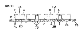
- FIGS. 13A to 13D are schematic cross-sectional views showing the recovery process of the chip resistor after the process of FIG. 10I.
- FIG. 13A shows a state in which a plurality of chip resistors 1 that are separated into pieces are still attached to the support tape 71.
- a thermal foam sheet 73 is attached to the back surface 2 ⁇ / b> B of the substrate 2 of each chip resistor 1.
- the thermal foam sheet 73 includes a sheet-like sheet main body 74 and a large number of foam particles 75 kneaded in the sheet main body 74.
- the adhesive strength of the sheet body 74 is stronger than the adhesive strength on the adhesive surface 72 of the support tape 71. Therefore, after sticking the thermal foam sheet 73 to the back surface 2B of the substrate 2 of each chip resistor 1, the support tape 71 is peeled off from each chip resistor 1 as shown in FIG. Transfer to the thermal foam sheet 73. At this time, if the support tape 71 is irradiated with ultraviolet rays (see the dotted arrow in FIG. 13B), the adhesiveness of the adhesive surface 72 is lowered, so that the support tape 71 is easily peeled off from each chip resistor 1.
- the processing time can be shortened compared to the case where the chip resistors 1 are peeled off from the support tape 71 or the thermal foam sheet 73 one by one.
- a predetermined number of chip resistors 1 may be directly peeled off from the support tape 71 without using the thermal foam sheet 73.
- FIGS. 14A to 14C are schematic cross-sectional views showing a chip resistor recovery step (modified example) after the step of FIG. 10I.
- Each chip resistor 1 can be recovered by another method shown in FIGS. 14A to 14C.
- FIG. 14A shows a state where a plurality of separated chip resistors 1 are still attached to the support tape 71 as in FIG. 13A.
- a transfer tape 77 is attached to the back surface 2B of the substrate 2 of each chip resistor 1.
- the transfer tape 77 has a stronger adhesive force than the adhesive surface 72 of the support tape 71. Therefore, as shown in FIG. 14C, after attaching the transfer tape 77 to each chip resistor 1, the support tape 71 is peeled off from each chip resistor 1.
- the support tape 71 may be irradiated with ultraviolet rays (see the dotted arrow in FIG. 14B) in order to reduce the adhesiveness of the adhesive surface 72.
- Frames 78 of a collection device are attached to both ends of the transfer tape 77.
- the frames 78 on both sides can move in directions toward or away from each other.
- the transfer tape 77 expands and becomes thin.
- the adhesive force of the transfer tape 77 is reduced, so that each chip resistor 1 is easily peeled off from the transfer tape 77.
- the suction nozzle 76 of the transport device (not shown) is directed toward the element forming surface 2A side of the chip resistor 1
- the chip resistor 1 is caused to be attracted by the suction force generated by the transport device (not shown).
- FIG. 15 is a plan view of a chip capacitor according to another embodiment of the present invention.
- 16 is a cross-sectional view taken along section line XVI-XVI in FIG.
- FIG. 17 is an exploded perspective view showing a part of the structure of the chip capacitor separately.
- the chip capacitor 101 similarly to the chip resistor 1, the chip capacitor 101 includes the substrate 2, the first connection electrode 3 disposed on the substrate 2 (on the element formation surface 2 ⁇ / b> A side), and the substrate 2 and the 2nd connection electrode 4 arrange
- the substrate 2 has a rectangular shape in plan view.
- the first connection electrode 3 and the second connection electrode 4 are respectively disposed at both ends in the longitudinal direction of the substrate 2.
- the first connection electrode 3 and the second connection electrode 4 have a substantially rectangular planar shape extending in the short direction of the substrate 2.
- the first connection electrode 3 and the second connection electrode 4 are integrally formed on the element formation surface 2A and the side surfaces 2C to 2F so as to cover the peripheral edge portion 85.
- a plurality of capacitor elements C1 to C9 are formed in a capacitor arrangement region 105 between the first connection electrode 3 and the second connection electrode 4.
- the plurality of capacitor elements C1 to C9 are a plurality of element elements constituting the element 5 (capacitor element here), and are connected between the first connection electrode 3 and the second connection electrode 4.
- the plurality of capacitor elements C1 to C9 are electrically connected so as to be separable from the second connection electrode 4 through a plurality of fuse units 107 (corresponding to the fuse F described above). Yes.
- the upper electrode film 113 is formed on the capacitor film 112. In FIG. 15, for clarity, the upper electrode film 113 is colored.
- the upper electrode film 113 includes a capacitor electrode region 113A located in the capacitor arrangement region 105, a pad region 113B located immediately below the second connection electrode 4 and in contact with the second connection electrode 4, and the capacitor electrode region 113A and the pad region. 113B and a fuse region 113C disposed between them.
- the ratio of the capacitance values of the capacitor elements C1 to C9 is equal to the ratio of the facing areas, and is 1: 2: 4: 8: 16: 32. : 64: 128: 128. That is, the plurality of capacitor elements C1 to C9 include a plurality of capacitor elements C1 to C8 (or C1 to C7, C9) having capacitance values set so as to form a geometric sequence with a common ratio of 2.
- the electrode film portions 131 to 135 are formed in a strip shape having the same width and a length ratio set to 1: 2: 4: 8: 16.
- the electrode film portions 135, 136, 137, 138, and 139 are formed in a strip shape having the same length and the width ratio set to 1: 2: 4: 8: 8.
- the electrode film portions 135 to 139 are formed to extend over a range from the edge on the second connection electrode 4 side of the capacitor arrangement region 105 to the edge on the first connection electrode 3 side. 134 is formed shorter than that.
- the pad region 113B is formed in a substantially similar shape to the second connection electrode 4 and has a substantially rectangular planar shape. As shown in FIG. 16, the upper electrode film 113 in the pad region 113 ⁇ / b> B is in contact with the second connection electrode 4.
- the fuse unit 107 includes a first wide portion 107A for connection to the pad region 113B, a second wide portion 107B for connection to the electrode film portions 131 to 139, and the first and second wide portions 107A and 7B. And a narrow portion 107 ⁇ / b> C that connects the two.
- the narrow portion 107C is configured to be cut (fused) by laser light. Accordingly, unnecessary electrode film portions of the electrode film portions 131 to 139 can be electrically disconnected from the first and second connection electrodes 3 and 4 by cutting the fuse unit 107.
- the passivation film 23 and the resin film 24 are protective films that protect the surface of the chip capacitor 101.
- the notches 25 described above are formed in regions corresponding to the first connection electrode 3 and the second connection electrode 4, respectively.
- the notch 25 penetrates the passivation film 23 and the resin film 24.
- the notch 25 corresponding to the first connection electrode 3 also penetrates the capacitive film 112.
- the first connection electrode 3 and the second connection electrode 4 are embedded in the notch 25, respectively. Accordingly, the first connection electrode 3 is bonded to the pad region 111B of the lower electrode film 111, and the second connection electrode 4 is bonded to the pad region 113B of the upper electrode film 113.
- the first and second connection electrodes 3, 4 protrude from the surface of the resin film 24, and have a lead-out portion 27 drawn out to the inside of the substrate 2 (element 5 side) along the surface of the resin film 24. ing. Thereby, the chip capacitor 101 can be flip-chip bonded to the mounting substrate.
- FIG. 18 is a circuit diagram showing an internal electrical configuration of the chip capacitor.
- a plurality of capacitor elements C1 to C9 are connected in parallel between the first connection electrode 3 and the second connection electrode 4.
- fuses F1 to F9 each composed of one or a plurality of fuse units 107 are interposed in series.
- the capacitance value of the chip capacitor 101 is equal to the sum of the capacitance values of the capacitor elements C1 to C9.
- the capacitor element corresponding to the disconnected fuse is disconnected, and the capacitance of the chip capacitor 101 is equal to the capacitance value of the disconnected capacitor element. The value decreases.
- the capacitance value between the pad regions 111B and 113B (total capacitance value of the capacitor elements C1 to C9) is measured, and then one or more appropriately selected from the fuses F1 to F9 according to the desired capacitance value. If the fuse is blown with a laser beam, adjustment to a desired capacitance value (laser trimming) can be performed.
- the capacitance values of the capacitor elements C1 to C8 are set so as to form a geometric sequence with a common ratio of 2, the capacitor element C1 having the smallest capacitance value (the value of the first term of the geometric sequence) Fine adjustment is possible to match the target capacitance value with accuracy corresponding to the capacitance value.
- the capacitance values of the capacitor elements C1 to C9 may be determined as follows.
- the capacitance of the chip capacitor 101 can be finely adjusted with a minimum fitting accuracy of 0.03125 pF. Further, by appropriately selecting a fuse to be cut from the fuses F1 to F9, it is possible to provide the chip capacitor 101 having an arbitrary capacitance value between 10 pF and 18 pF.
- Capacitor arrangement region 105 is generally a square region having one side corresponding to the length of the short side of substrate 2.
- the thickness of the substrate 2 may be about 150 ⁇ m.
- substrate 2 may be, for example, a substrate that has been thinned by grinding or polishing from the back side (the surface on which capacitor elements C1 to C9 are not formed).
- a semiconductor substrate typified by a silicon substrate may be used, a glass substrate may be used, or a resin film may be used.
- the insulating film 20 may be an oxide film such as a silicon oxide film.
- the film thickness may be about 500 to 2000 mm.
- the capacitor film 112 can be made of, for example, a silicon nitride film, and can have a thickness of 500 to 2000 mm (for example, 1000 mm).
- the capacitor film 112 may be a silicon nitride film formed by plasma CVD (chemical vapor deposition).
- the passivation film 23 can be composed of, for example, a silicon nitride film, and can be formed by, for example, a plasma CVD method.
- the film thickness may be about 8000 mm.
- the resin film 24 can be composed of a polyimide film or other resin film.
- the first and second connection electrodes 3 and 4 include, for example, a nickel layer in contact with the lower electrode film 111 or the upper electrode film 113, a palladium layer stacked on the nickel layer, and a gold layer stacked on the palladium layer.
- a nickel layer contributes to improving the adhesion to the lower electrode film 111 or the upper electrode film 113
- the palladium layer is made of the material of the upper electrode film or the lower electrode film and the gold of the uppermost layer of the first and second connection electrodes 3 and 4. It functions as a diffusion preventing layer that suppresses mutual diffusion.
- the manufacturing process of such a chip capacitor 101 is the same as the manufacturing process of the chip resistor 1 after the element 5 is formed.
- an oxide film for example, a silicon oxide film
- An insulating film 20 is formed.
- the lower electrode film 111 made of an aluminum film is formed over the entire surface of the insulating film 20 by, eg, sputtering.
- the thickness of the lower electrode film 111 may be about 8000 mm.
- a resist pattern corresponding to the final shape of the lower electrode film 111 is formed on the surface of the lower electrode film by photolithography.
- the lower electrode film 111 having the pattern shown in FIG. 15 and the like is obtained by etching the lower electrode film using the resist pattern as a mask. Etching of the lower electrode film 111 can be performed by, for example, reactive ion etching.
- a capacitor film 112 made of a silicon nitride film or the like is formed on the lower electrode film 111 by, for example, a plasma CVD method. In the region where the lower electrode film 111 is not formed, the capacitor film 112 is formed on the surface of the insulating film 20.
- the upper electrode film 113 is formed on the capacitor film 112.
- the upper electrode film 113 is made of, for example, an aluminum film and can be formed by a sputtering method. The film thickness may be about 8000 mm.
- a resist pattern corresponding to the final shape of the upper electrode film 113 is formed on the surface of the upper electrode film 113 by photolithography.
- the upper electrode film 113 is patterned into a final shape (see FIG. 15 and the like). Accordingly, the upper electrode film 113 has a portion divided into a plurality of electrode film portions 131 to 139 in the capacitor electrode region 113A, and has a plurality of fuse units 107 in the fuse region 113C. A pattern having the connected pad region 113B is shaped. Etching for patterning the upper electrode film 113 may be performed by wet etching using an etchant such as phosphoric acid or by reactive ion etching.
- an etchant such as phosphoric acid
- the element 5 (capacitor elements C1 to C9 and the fuse unit 107) in the chip capacitor 101 is formed.
- laser trimming for fusing the fuse unit 107 is performed (see FIG. 10B). That is, a laser beam is applied to the fuse unit 107 constituting the fuse selected according to the measurement result of the total capacity value, and the narrow portion 107C (see FIG. 15) of the fuse unit 107 is blown. As a result, the corresponding capacitor element is separated from the pad region 113B.
- the energy of the laser light is accumulated in the vicinity of the fuse unit 107 by the action of the insulating film 45 which is a cover film, and thereby the fuse unit 107 is melted. Thereby, the capacitance value of the chip capacitor 101 can be reliably set to the target capacitance value.
- chip parts (chip resistor 1 and chip capacitor 101) of the present invention have been described above, but the present invention can be implemented in other forms.
- the common ratio of the geometric sequence may be a number other than two.
- the common ratio of the geometric sequence may be a number other than two.
- the insulating film 20 is formed on the surface of the substrate 2. However, if the substrate 2 is an insulating substrate, the insulating film 20 can be omitted.
- the chip capacitor 101 only the upper electrode film 113 is divided into a plurality of electrode film portions. However, only the lower electrode film 111 is divided into a plurality of electrode film portions, or the upper electrode film 113 is divided. Both the lower electrode film 111 and the lower electrode film 111 may be divided into a plurality of electrode film portions. Furthermore, in the above-described embodiment, an example in which the upper electrode film or the lower electrode film and the fuse unit are integrated is shown. However, the fuse unit is formed of a conductor film different from the upper electrode film or the lower electrode film. May be. In the above-described chip capacitor 101, a single-layer capacitor structure having the upper electrode film 113 and the lower electrode film 111 is formed. Another electrode film is laminated on the upper electrode film 113 through a capacitive film. Thus, a plurality of capacitor structures may be stacked.
- the element 5 formed on the substrate 2 in the chip inductor includes an inductor element including a plurality of inductor elements (element elements), and the first connection electrode 3 and the second connection electrode 4.
- the element 5 is provided in the multilayer wiring of the multilayer substrate described above, and is formed by the wiring film 22.
- the plurality of fuses F described above are provided on the substrate 2, and each inductor element can be separated from the first connection electrode 3 and the second connection electrode 4 via the fuse F. It is connected to the.
- a combination pattern of a plurality of inductor elements can be changed to an arbitrary pattern by selecting and cutting one or a plurality of fuses F. Therefore, chip inductors having various electrical characteristics can be obtained. Can be realized with a common design.
- the element 5 formed on the substrate 2 in the chip diode includes a diode network (diode element) including a plurality of diode elements (element elements). .
- the diode element is formed on the substrate 2.
- this chip diode by selecting and cutting one or a plurality of fuses F, a combination pattern of a plurality of diode elements in the diode network can be changed to an arbitrary pattern.
- various chip diodes can be realized with a common design.
- Both the chip inductor and the chip diode can achieve the same effects as the chip resistor 1 and the chip capacitor 101.
- the Pd layer 34 interposed between the Ni layer 33 and the Au layer 35 can be omitted. Since the adhesion between the Ni layer 33 and the Au layer 35 is good, the Pd layer 34 may be omitted if the above-described pinhole cannot be formed in the Au layer 35.
- FIG. 19 is a perspective view showing an appearance of a smartphone which is an example of an electronic device in which the chip component of the present invention is used.
- the smartphone 201 is configured by housing electronic components in a flat rectangular parallelepiped casing 202.
- the housing 202 has a pair of rectangular main surfaces on the front side and the back side, and the pair of main surfaces are joined by four side surfaces.
- the display surface of the display panel 203 configured by a liquid crystal panel, an organic EL panel, or the like is exposed.
- the display surface of the display panel 203 forms a touch panel and provides an input interface for the user.
- the display panel 203 is formed in a rectangular shape that occupies most of one main surface of the housing 202.
- Operation buttons 204 are arranged along one short side of the display panel 203.
- a plurality (three) of operation buttons 204 are arranged along the short side of the display panel 203.
- the user can operate the smartphone 201 by operating the operation buttons 204 and the touch panel, and call and execute necessary functions.
- FIG. 20 is a schematic plan view showing the configuration of the circuit assembly 100 housed in the housing 202.
- the circuit assembly 100 includes the mounting board 9 described above and circuit components mounted on the mounting surface 9A of the mounting board 9.
- the plurality of circuit components include a plurality of integrated circuit elements (ICs) 212-220 and a plurality of chip components.
- the plurality of ICs include a transmission processing IC 212, a one-segment TV reception IC 213, a GPS reception IC 214, an FM tuner IC 215, a power supply IC 216, a flash memory 217, a microcomputer 218, a power supply IC 219, and a baseband IC 220.
- the plurality of chip components (corresponding to the chip components of the present invention) include chip inductors 221, 225, 235, chip resistors 222, 224, 233, chip capacitors 227, 230, 234, and chip diodes 228, 231.
- the transmission processing IC 212 includes an electronic circuit for generating a display control signal for the display panel 203 and receiving an input signal from the touch panel on the surface of the display panel 203.
- a flexible wiring 209 is connected to the transmission processing IC 212 for connection with the display panel 203.
- the 1Seg TV reception IC 213 incorporates an electronic circuit that constitutes a receiver for receiving radio waves of 1Seg broadcast (terrestrial digital television broadcast targeted for mobile devices).
- 1Seg broadcast terrestrial digital television broadcast targeted for mobile devices.
- a plurality of chip inductors 221 and a plurality of chip resistors 222 are arranged.
- the one-segment TV reception IC 213, the chip inductor 221 and the chip resistor 222 constitute a one-segment broadcast reception circuit 223.
- the chip inductor 221 and the chip resistor 222 respectively have an inductance and a resistance that are accurately matched, and give a highly accurate circuit constant to the one-segment broadcasting reception circuit 223.
- the GPS reception IC 214 contains an electronic circuit that receives radio waves from GPS satellites and outputs position information of the smartphone 201.
- a plurality of chip capacitors 227 and a plurality of chip diodes 228 are mounted on the mounting surface of the mounting substrate 9.
- the power supply IC 216 forms a power supply circuit 229 together with the chip capacitor 227 and the chip diode 228.
- the flash memory 217 is a storage device for recording an operating system program, data generated inside the smartphone 201, data and programs acquired from the outside by a communication function, and the like.
- a plurality of chip capacitors 230 and a plurality of chip diodes 231 are mounted on the mounting surface of the mounting substrate 9 near the power supply IC 219.
- the power supply IC 219 constitutes a power supply circuit 232 together with the chip capacitor 230 and the chip diode 231.
- the baseband IC 220 forms a baseband communication circuit 236 together with the chip resistor 233, the chip capacitor 234, and the chip inductor 235.
- the baseband communication circuit 236 provides a communication function for telephone communication and data communication.
- the power appropriately adjusted by the power supply circuits 229 and 232 is transmitted to the transmission processing IC 212, the GPS reception IC 214, the one-segment broadcast reception circuit 223, the FM broadcast reception circuit 226, the baseband communication circuit 236, the flash memory 217, and the like. It is supplied to the microcomputer 218.
- the microcomputer 218 performs arithmetic processing in response to an input signal input via the transmission processing IC 212 and outputs a display control signal from the transmission processing IC 212 to the display panel 203 to cause the display panel 203 to perform various displays. .
- the one-segment broadcasting is received by the function of the one-segment broadcasting receiving circuit 223. Then, the microcomputer 218 executes arithmetic processing for outputting the received image to the display panel 203 and making the received sound audible from the speaker 205.
- the microcomputer 218 acquires the position information output from the GPS reception IC 214 and executes a calculation process using the position information.
- the flash memory 217 is used for storing data obtained by communication, calculation by the microcomputer 218, and data created by input from the touch panel.
- the microcomputer 218 writes data to the flash memory 217 and reads data from the flash memory 217 as necessary.
- the function of telephone communication or data communication is realized by the baseband communication circuit 236.
- the microcomputer 218 controls the baseband communication circuit 236 to perform processing for transmitting and receiving voice or data.
Landscapes
- Engineering & Computer Science (AREA)
- Power Engineering (AREA)
- Microelectronics & Electronic Packaging (AREA)
- Manufacturing & Machinery (AREA)
- Apparatuses And Processes For Manufacturing Resistors (AREA)
- Chemical & Material Sciences (AREA)
- Non-Adjustable Resistors (AREA)
- Ceramic Engineering (AREA)
- Inorganic Chemistry (AREA)
- Physics & Mathematics (AREA)
- Electromagnetism (AREA)
- Fixed Capacitors And Capacitor Manufacturing Machines (AREA)
- Ceramic Capacitors (AREA)
- Materials Engineering (AREA)
- Details Of Resistors (AREA)
Description
C2=0.0625pF
C3=0.125pF
C4=0.25pF
C5=0.5pF
C6=1pF
C7=2pF
C8=4pF
C9=4pF
この場合、0.03125pFの最小合わせ込み精度でチップコンデンサ101の容量を微調整できる。また、ヒューズF1~F9から切断すべきヒューズを適切に選択することで、10pF~18pFの間の任意の容量値のチップコンデンサ101を提供することができる。
2 基板
2A 素子形成面
2C 側面
2D 側面
2E 側面
2F 側面
3 第1接続電極
4 第2接続電極
5 素子
9 実装基板
9A 実装面
13 半田
21 抵抗体膜
22 配線膜
23 パッシベーション膜
24 樹脂膜
27 引き出し部
33 Ni層
34 Pd層
35 Au層
45 絶縁膜
46 樹脂膜
47 絶縁膜
56 抵抗
85 周縁部
88 ランド
100 回路アセンブリ
101 チップコンデンサ
221 チップインダクタ
222 チップ抵抗器
224 チップ抵抗器
225 チップインダクタ
227 チップコンデンサ
228 チップダイオード
230 チップコンデンサ
231 チップダイオード
233 チップ抵抗器
234 チップコンデンサ
235 チップインダクタ
C1~C9 キャパシタ要素
F(F1~F9) ヒューズ
R 抵抗体
Claims (20)
- 表面および側面を有する基板と、
前記基板の前記表面の縁部を覆うように、当該表面および前記側面に一体的に形成された電極と、
前記電極と前記基板との間に介在された絶縁膜とを含む、チップ部品。 - 前記基板は平面視において矩形状であり、
前記電極は、前記基板の三方の前記縁部を覆うように形成されている、請求項1に記載のチップ部品。 - 前記基板の前記表面において前記縁部から間隔を空けて形成され、前記電極が電気的に接続された配線膜をさらに含む、請求項1または2に記載のチップ部品。
- 前記配線膜は、前記電極に覆われた前記基板の前記縁部に対向する周縁部が選択的に露出しており、当該露出部分を除く周縁部が樹脂膜で選択的に覆われている、請求項3に記載のチップ部品。
- 前記電極は、前記樹脂膜の表面から突出するように形成されている、請求項4に記載のチップ部品。
- 前記電極は、前記樹脂膜の前記表面に沿って横方向に引き出され、当該表面を選択的に覆う引き出し部を含む、請求項5に記載のチップ部品。
- 前記電極が、Ni層と、Au層とを含み、前記Au層が最表面に露出している、請求項1~6のいずれか一項に記載のチップ部品。
- 前記電極が、前記Ni層と前記Au層との間に介装されたPd層をさらに含む、請求項7に記載のチップ部品。
- 前記電極が互いに間隔を空けて2つ設けられており、
前記チップ部品は、前記基板上に形成され前記2つの電極間に接続された抵抗体を含むチップ抵抗器である、請求項1~8のいずれか一項に記載のチップ部品。 - 複数の前記抵抗体と、前記基板上に設けられ、前記複数の抵抗体をそれぞれ切り離し可能に前記電極に接続する複数のヒューズとをさらに含む、請求項9に記載のチップ部品。
- 前記電極が互いに間隔を空けて2つ設けられており、
前記チップ部品は、前記基板上に形成され前記2つの電極の間に接続されたキャパシタ素子を含むチップコンデンサである、請求項1~8のいずれか一項に記載のチップ部品。 - 前記キャパシタ素子を構成する複数のキャパシタ要素と、前記基板上に設けられ、前記複数のキャパシタ要素をそれぞれ切り離し可能に前記電極に接続する複数のヒューズとをさらに含む、請求項11に記載のチップ部品。
- 請求項1~12のいずれか一項に記載のチップ部品と、
前記基板の前記表面に対向する実装面に、前記電極に半田接合されたランドを有する実装基板とを含む、回路アセンブリ。 - 前記実装面の法線方向から見たときに、前記半田が前記電極の表面部分および側面部分を覆うように形成されている、請求項13に記載の回路アセンブリ。
- 請求項13または14に記載の回路アセンブリと、
前記回路アセンブリを収容した筐体とを含む、電子機器。 - 基板の複数のチップ部品領域の境界領域に前記基板の表面から所定深さの溝を形成して、前記複数のチップ部品領域毎の基板に分離する工程と、
前記溝の側面に絶縁膜を形成することにより、各基板の側面に当該絶縁膜を形成する工程と、
前記各基板の前記表面からその縁部を介して前記溝の前記側面に沿って前記絶縁膜上に電極材料をめっき成長させることによって、前記各基板の前記表面の前記縁部を覆うように、当該表面および前記側面に電極を一体的に形成する工程と、
前記基板の裏面を前記溝に到達するまで研削して、前記基板を複数のチップ部品に分割する工程とを含む、チップ部品の製造方法。 - 前記電極を形成する工程は、前記電極材料を無電解めっきによって成長させる工程を含む、請求項16に記載のチップ部品の製造方法。
- 前記複数のチップ部品領域毎に前記基板の前記表面に配線膜を形成する工程をさらに含み、
前記基板に分離する工程は、前記各基板の前記縁部と前記配線膜との間に間隔が空くように前記溝を形成する工程を含み、
前記電極を形成する工程は、前記配線膜から前記電極材料をめっき成長させる工程を含む、請求項16または17に記載のチップ部品の製造方法。 - 前記溝の形成前に前記配線膜を覆う樹脂膜を形成する工程と、
前記配線膜における前記溝を形成すべき領域に対向する周縁部が露出するように、前記樹脂膜を選択的に除去する工程とをさらに含む、請求項18に記載のチップ部品の製造方法。 - 前記溝の形成が、エッチングによって行われる、請求項16~19のいずれか一項に記載のチップ部品の製造方法。
Priority Applications (4)
| Application Number | Priority Date | Filing Date | Title |
|---|---|---|---|
| US14/431,771 US9583238B2 (en) | 2012-09-27 | 2013-08-07 | Chip component and production method therefor |
| KR1020157010367A KR102071746B1 (ko) | 2012-09-27 | 2013-08-07 | 칩 부품 및 그 제조 방법 |
| CN201380050045.3A CN104704583B (zh) | 2012-09-27 | 2013-08-07 | 贴片部件及其制造方法 |
| US15/408,864 US10312002B2 (en) | 2012-09-27 | 2017-01-18 | Chip component and production method therefor |
Applications Claiming Priority (2)
| Application Number | Priority Date | Filing Date | Title |
|---|---|---|---|
| JP2012-215062 | 2012-09-27 | ||
| JP2012215062A JP2014072242A (ja) | 2012-09-27 | 2012-09-27 | チップ部品およびその製造方法 |
Related Child Applications (2)
| Application Number | Title | Priority Date | Filing Date |
|---|---|---|---|
| US14/431,771 A-371-Of-International US9583238B2 (en) | 2012-09-27 | 2013-08-07 | Chip component and production method therefor |
| US15/408,864 Continuation US10312002B2 (en) | 2012-09-27 | 2017-01-18 | Chip component and production method therefor |
Publications (1)
| Publication Number | Publication Date |
|---|---|
| WO2014050322A1 true WO2014050322A1 (ja) | 2014-04-03 |
Family
ID=50387736
Family Applications (1)
| Application Number | Title | Priority Date | Filing Date |
|---|---|---|---|
| PCT/JP2013/071412 Ceased WO2014050322A1 (ja) | 2012-09-27 | 2013-08-07 | チップ部品およびその製造方法 |
Country Status (5)
| Country | Link |
|---|---|
| US (2) | US9583238B2 (ja) |
| JP (1) | JP2014072242A (ja) |
| KR (1) | KR102071746B1 (ja) |
| CN (1) | CN104704583B (ja) |
| WO (1) | WO2014050322A1 (ja) |
Cited By (2)
| Publication number | Priority date | Publication date | Assignee | Title |
|---|---|---|---|---|
| JP2015130492A (ja) * | 2013-12-05 | 2015-07-16 | ローム株式会社 | 半導体モジュール |
| JPWO2021221087A1 (ja) * | 2020-05-01 | 2021-11-04 |
Families Citing this family (6)
| Publication number | Priority date | Publication date | Assignee | Title |
|---|---|---|---|---|
| JP6557468B2 (ja) | 2014-12-25 | 2019-08-07 | ローム株式会社 | チップ部品 |
| JP6674677B2 (ja) * | 2016-02-17 | 2020-04-01 | ローム株式会社 | チップ部品およびその製造方法 |
| JP2017195225A (ja) * | 2016-04-18 | 2017-10-26 | ローム株式会社 | チップ抵抗器 |
| US10607779B2 (en) * | 2016-04-22 | 2020-03-31 | Rohm Co., Ltd. | Chip capacitor having capacitor region directly below external electrode |
| US11129906B1 (en) | 2016-12-07 | 2021-09-28 | David Gordon Bermudes | Chimeric protein toxins for expression by therapeutic bacteria |
| US11056253B2 (en) * | 2019-03-18 | 2021-07-06 | Qualcomm Incorporated | Thin-film resistors with flexible terminal placement for area saving |
Citations (5)
| Publication number | Priority date | Publication date | Assignee | Title |
|---|---|---|---|---|
| JPH0513201A (ja) * | 1991-07-05 | 1993-01-22 | Matsushita Electric Ind Co Ltd | 角形チツプ抵抗器 |
| JPH09323300A (ja) * | 1996-06-07 | 1997-12-16 | Rohm Co Ltd | 基板分割方法 |
| JP2002231120A (ja) * | 2001-02-05 | 2002-08-16 | Skk:Kk | チップ型電子部品 |
| JP2006024767A (ja) * | 2004-07-08 | 2006-01-26 | Koa Corp | チップ抵抗器の製造方法 |
| JP2012102169A (ja) * | 2010-11-08 | 2012-05-31 | Sumitomo Bakelite Co Ltd | エポキシ樹脂組成物、プリプレグ、金属張積層板、プリント配線板および半導体装置 |
Family Cites Families (22)
| Publication number | Priority date | Publication date | Assignee | Title |
|---|---|---|---|---|
| US3778886A (en) * | 1972-01-20 | 1973-12-18 | Signetics Corp | Semiconductor structure with fusible link and method |
| US4298856A (en) * | 1979-09-04 | 1981-11-03 | Western Electric Company, Incorporated | Metallized resistor and methods of manufacturing and adjusting the resistance of same |
| US4862136A (en) * | 1983-04-13 | 1989-08-29 | Birkner John M | Programmable resistance network |
| JP3307533B2 (ja) * | 1996-05-14 | 2002-07-24 | アルプス電気株式会社 | チップ電子部品とその製造方法、およびサージアブソーバとその製造方法 |
| CN1160742C (zh) * | 1997-07-03 | 2004-08-04 | 松下电器产业株式会社 | 电阻器及其制造方法 |
| US6060760A (en) * | 1997-08-13 | 2000-05-09 | Tritech Microelectronics, Ltd. | Optimal resistor network layout |
| TW424245B (en) * | 1998-01-08 | 2001-03-01 | Matsushita Electric Industrial Co Ltd | Resistor and its manufacturing method |
| JP2001076912A (ja) | 1999-09-06 | 2001-03-23 | Rohm Co Ltd | チップ抵抗器におけるレーザトリミング方法 |
| WO2001093283A1 (en) * | 2000-06-02 | 2001-12-06 | Koninklijke Philips Electronics N.V. | Passive component |
| JP2003158002A (ja) * | 2001-11-22 | 2003-05-30 | Matsushita Electric Ind Co Ltd | チップ型電子部品とその製造方法 |
| AU2002324848A1 (en) * | 2002-09-03 | 2004-03-29 | Vishay Intertechnology, Inc. | Flip chip resistor and its manufacturing method |
| JP4427960B2 (ja) | 2003-03-25 | 2010-03-10 | 株式会社村田製作所 | 薄膜積層電子部品の製造方法 |
| JP4406300B2 (ja) * | 2004-02-13 | 2010-01-27 | 株式会社東芝 | 半導体装置及びその製造方法 |
| JP2005251904A (ja) * | 2004-03-03 | 2005-09-15 | Denso Corp | 基板表面実装部品、基板回路、基板、ハンダ接続方法、及び基板回路の製造方法 |
| US7259703B2 (en) * | 2004-03-25 | 2007-08-21 | Texas Instruments Incorporated | Device for recording laser trim progress and for detecting laser beam misalignment |
| JP4716099B2 (ja) * | 2005-09-30 | 2011-07-06 | 三菱マテリアル株式会社 | チップ型ヒューズの製造方法 |
| JP2008021726A (ja) * | 2006-07-11 | 2008-01-31 | Ricoh Co Ltd | トリミング回路及び半導体装置 |
| JP4353258B2 (ja) * | 2007-02-20 | 2009-10-28 | セイコーエプソン株式会社 | 抵抗回路及び発振回路 |
| JP5433957B2 (ja) * | 2008-02-26 | 2014-03-05 | 株式会社リコー | 半導体装置 |
| JP5549066B2 (ja) * | 2008-09-30 | 2014-07-16 | 凸版印刷株式会社 | リードフレーム型基板とその製造方法、及び半導体装置 |
| JP2010161135A (ja) * | 2009-01-07 | 2010-07-22 | Rohm Co Ltd | チップ抵抗器およびその製造方法 |
| JP2011086750A (ja) | 2009-10-15 | 2011-04-28 | Panasonic Corp | 薄膜チップ抵抗器 |
-
2012
- 2012-09-27 JP JP2012215062A patent/JP2014072242A/ja active Pending
-
2013
- 2013-08-07 KR KR1020157010367A patent/KR102071746B1/ko not_active Expired - Fee Related
- 2013-08-07 CN CN201380050045.3A patent/CN104704583B/zh active Active
- 2013-08-07 WO PCT/JP2013/071412 patent/WO2014050322A1/ja not_active Ceased
- 2013-08-07 US US14/431,771 patent/US9583238B2/en active Active
-
2017
- 2017-01-18 US US15/408,864 patent/US10312002B2/en active Active
Patent Citations (5)
| Publication number | Priority date | Publication date | Assignee | Title |
|---|---|---|---|---|
| JPH0513201A (ja) * | 1991-07-05 | 1993-01-22 | Matsushita Electric Ind Co Ltd | 角形チツプ抵抗器 |
| JPH09323300A (ja) * | 1996-06-07 | 1997-12-16 | Rohm Co Ltd | 基板分割方法 |
| JP2002231120A (ja) * | 2001-02-05 | 2002-08-16 | Skk:Kk | チップ型電子部品 |
| JP2006024767A (ja) * | 2004-07-08 | 2006-01-26 | Koa Corp | チップ抵抗器の製造方法 |
| JP2012102169A (ja) * | 2010-11-08 | 2012-05-31 | Sumitomo Bakelite Co Ltd | エポキシ樹脂組成物、プリプレグ、金属張積層板、プリント配線板および半導体装置 |
Cited By (4)
| Publication number | Priority date | Publication date | Assignee | Title |
|---|---|---|---|---|
| JP2015130492A (ja) * | 2013-12-05 | 2015-07-16 | ローム株式会社 | 半導体モジュール |
| JPWO2021221087A1 (ja) * | 2020-05-01 | 2021-11-04 | ||
| JP7420230B2 (ja) | 2020-05-01 | 2024-01-23 | 株式会社村田製作所 | 半導体装置及びモジュール |
| US12520508B2 (en) | 2020-05-01 | 2026-01-06 | Murata Manufacturing Co., Ltd. | Enhanced low-loss semiconductor capacitor device featuring asymmetric electrode shielding architecture |
Also Published As
| Publication number | Publication date |
|---|---|
| CN104704583B (zh) | 2018-05-04 |
| KR20150064100A (ko) | 2015-06-10 |
| US9583238B2 (en) | 2017-02-28 |
| JP2014072242A (ja) | 2014-04-21 |
| US20150243412A1 (en) | 2015-08-27 |
| US20170125140A1 (en) | 2017-05-04 |
| KR102071746B1 (ko) | 2020-01-30 |
| US10312002B2 (en) | 2019-06-04 |
| CN104704583A (zh) | 2015-06-10 |
Similar Documents
| Publication | Publication Date | Title |
|---|---|---|
| WO2014050322A1 (ja) | チップ部品およびその製造方法 | |
| US10593480B2 (en) | Chip capacitor, circuit assembly, and electronic device | |
| US10681815B2 (en) | Composite chip component, circuit assembly and electronic apparatus | |
| JP6259184B2 (ja) | チップ部品およびその製造方法 | |
| JP6245811B2 (ja) | チップ部品およびその製造方法 | |
| JP6547932B2 (ja) | チップ部品およびその製造方法、ならびに当該チップ部品を備えた回路アセンブリおよび電子機器 | |
| JP2014072241A (ja) | チップ部品 | |
| JP6584574B2 (ja) | チップ部品およびその製造方法 | |
| JP2017130671A (ja) | チップ部品 | |
| JP6101465B2 (ja) | チップ部品 | |
| JP2018006771A (ja) | チップ部品 | |
| JP6535073B2 (ja) | チップ部品 | |
| JP2014072239A (ja) | チップ部品 | |
| JP7063845B2 (ja) | チップ抵抗器 |
Legal Events
| Date | Code | Title | Description |
|---|---|---|---|
| 121 | Ep: the epo has been informed by wipo that ep was designated in this application |
Ref document number: 13840524 Country of ref document: EP Kind code of ref document: A1 |
|
| WWE | Wipo information: entry into national phase |
Ref document number: 14431771 Country of ref document: US |
|
| NENP | Non-entry into the national phase |
Ref country code: DE |
|
| ENP | Entry into the national phase |
Ref document number: 20157010367 Country of ref document: KR Kind code of ref document: A |
|
| 122 | Ep: pct application non-entry in european phase |
Ref document number: 13840524 Country of ref document: EP Kind code of ref document: A1 |