WO2014034741A1 - 異方性導電フィルム及びその製造方法 - Google Patents
異方性導電フィルム及びその製造方法 Download PDFInfo
- Publication number
- WO2014034741A1 WO2014034741A1 PCT/JP2013/073053 JP2013073053W WO2014034741A1 WO 2014034741 A1 WO2014034741 A1 WO 2014034741A1 JP 2013073053 W JP2013073053 W JP 2013073053W WO 2014034741 A1 WO2014034741 A1 WO 2014034741A1
- Authority
- WO
- WIPO (PCT)
- Prior art keywords
- anisotropic conductive
- film
- conductive film
- particle
- electronic component
- Prior art date
- Legal status (The legal status is an assumption and is not a legal conclusion. Google has not performed a legal analysis and makes no representation as to the accuracy of the status listed.)
- Ceased
Links
Images



Classifications
-
- C—CHEMISTRY; METALLURGY
- C08—ORGANIC MACROMOLECULAR COMPOUNDS; THEIR PREPARATION OR CHEMICAL WORKING-UP; COMPOSITIONS BASED THEREON
- C08J—WORKING-UP; GENERAL PROCESSES OF COMPOUNDING; AFTER-TREATMENT NOT COVERED BY SUBCLASSES C08B, C08C, C08F, C08G or C08H
- C08J5/00—Manufacture of articles or shaped materials containing macromolecular substances
- C08J5/18—Manufacture of films or sheets
-
- H—ELECTRICITY
- H01—ELECTRIC ELEMENTS
- H01R—ELECTRICALLY-CONDUCTIVE CONNECTIONS; STRUCTURAL ASSOCIATIONS OF A PLURALITY OF MUTUALLY-INSULATED ELECTRICAL CONNECTING ELEMENTS; COUPLING DEVICES; CURRENT COLLECTORS
- H01R43/00—Apparatus or processes specially adapted for manufacturing, assembling, maintaining, or repairing of line connectors or current collectors or for joining electric conductors
-
- H—ELECTRICITY
- H05—ELECTRIC TECHNIQUES NOT OTHERWISE PROVIDED FOR
- H05K—PRINTED CIRCUITS; CASINGS OR CONSTRUCTIONAL DETAILS OF ELECTRIC APPARATUS; MANUFACTURE OF ASSEMBLAGES OF ELECTRICAL COMPONENTS
- H05K3/00—Apparatus or processes for manufacturing printed circuits
- H05K3/30—Assembling printed circuits with electric components, e.g. with resistors
- H05K3/32—Assembling printed circuits with electric components, e.g. with resistors electrically connecting electric components or wires to printed circuits
- H05K3/321—Assembling printed circuits with electric components, e.g. with resistors electrically connecting electric components or wires to printed circuits by conductive adhesives
- H05K3/323—Assembling printed circuits with electric components, e.g. with resistors electrically connecting electric components or wires to printed circuits by conductive adhesives by applying an anisotropic conductive adhesive layer over an array of pads
-
- C—CHEMISTRY; METALLURGY
- C09—DYES; PAINTS; POLISHES; NATURAL RESINS; ADHESIVES; COMPOSITIONS NOT OTHERWISE PROVIDED FOR; APPLICATIONS OF MATERIALS NOT OTHERWISE PROVIDED FOR
- C09D—COATING COMPOSITIONS, e.g. PAINTS, VARNISHES OR LACQUERS; FILLING PASTES; CHEMICAL PAINT OR INK REMOVERS; INKS; CORRECTING FLUIDS; WOODSTAINS; PASTES OR SOLIDS FOR COLOURING OR PRINTING; USE OF MATERIALS THEREFOR
- C09D123/00—Coating compositions based on homopolymers or copolymers of unsaturated aliphatic hydrocarbons having only one carbon-to-carbon double bond; Coating compositions based on derivatives of such polymers
- C09D123/02—Coating compositions based on homopolymers or copolymers of unsaturated aliphatic hydrocarbons having only one carbon-to-carbon double bond; Coating compositions based on derivatives of such polymers not modified by chemical after-treatment
- C09D123/04—Homopolymers or copolymers of ethene
- C09D123/08—Copolymers of ethene
- C09D123/0846—Copolymers of ethene with unsaturated hydrocarbons containing other atoms than carbon or hydrogen atoms
- C09D123/0853—Vinylacetate
-
- C—CHEMISTRY; METALLURGY
- C09—DYES; PAINTS; POLISHES; NATURAL RESINS; ADHESIVES; COMPOSITIONS NOT OTHERWISE PROVIDED FOR; APPLICATIONS OF MATERIALS NOT OTHERWISE PROVIDED FOR
- C09J—ADHESIVES; NON-MECHANICAL ASPECTS OF ADHESIVE PROCESSES IN GENERAL; ADHESIVE PROCESSES NOT PROVIDED FOR ELSEWHERE; USE OF MATERIALS AS ADHESIVES
- C09J123/00—Adhesives based on homopolymers or copolymers of unsaturated aliphatic hydrocarbons having only one carbon-to-carbon double bond; Adhesives based on derivatives of such polymers
- C09J123/02—Adhesives based on homopolymers or copolymers of unsaturated aliphatic hydrocarbons having only one carbon-to-carbon double bond; Adhesives based on derivatives of such polymers not modified by chemical after-treatment
- C09J123/04—Homopolymers or copolymers of ethene
- C09J123/08—Copolymers of ethene
-
- C—CHEMISTRY; METALLURGY
- C09—DYES; PAINTS; POLISHES; NATURAL RESINS; ADHESIVES; COMPOSITIONS NOT OTHERWISE PROVIDED FOR; APPLICATIONS OF MATERIALS NOT OTHERWISE PROVIDED FOR
- C09J—ADHESIVES; NON-MECHANICAL ASPECTS OF ADHESIVE PROCESSES IN GENERAL; ADHESIVE PROCESSES NOT PROVIDED FOR ELSEWHERE; USE OF MATERIALS AS ADHESIVES
- C09J123/00—Adhesives based on homopolymers or copolymers of unsaturated aliphatic hydrocarbons having only one carbon-to-carbon double bond; Adhesives based on derivatives of such polymers
- C09J123/02—Adhesives based on homopolymers or copolymers of unsaturated aliphatic hydrocarbons having only one carbon-to-carbon double bond; Adhesives based on derivatives of such polymers not modified by chemical after-treatment
- C09J123/04—Homopolymers or copolymers of ethene
- C09J123/08—Copolymers of ethene
- C09J123/0846—Copolymers of ethene with unsaturated hydrocarbons containing other atoms than carbon or hydrogen atoms
- C09J123/0853—Vinylacetate
-
- C—CHEMISTRY; METALLURGY
- C09—DYES; PAINTS; POLISHES; NATURAL RESINS; ADHESIVES; COMPOSITIONS NOT OTHERWISE PROVIDED FOR; APPLICATIONS OF MATERIALS NOT OTHERWISE PROVIDED FOR
- C09J—ADHESIVES; NON-MECHANICAL ASPECTS OF ADHESIVE PROCESSES IN GENERAL; ADHESIVE PROCESSES NOT PROVIDED FOR ELSEWHERE; USE OF MATERIALS AS ADHESIVES
- C09J5/00—Adhesive processes in general; Adhesive processes not provided for elsewhere, e.g. relating to primers
- C09J5/06—Adhesive processes in general; Adhesive processes not provided for elsewhere, e.g. relating to primers involving heating of the applied adhesive
-
- C—CHEMISTRY; METALLURGY
- C09—DYES; PAINTS; POLISHES; NATURAL RESINS; ADHESIVES; COMPOSITIONS NOT OTHERWISE PROVIDED FOR; APPLICATIONS OF MATERIALS NOT OTHERWISE PROVIDED FOR
- C09J—ADHESIVES; NON-MECHANICAL ASPECTS OF ADHESIVE PROCESSES IN GENERAL; ADHESIVE PROCESSES NOT PROVIDED FOR ELSEWHERE; USE OF MATERIALS AS ADHESIVES
- C09J7/00—Adhesives in the form of films or foils
-
- C—CHEMISTRY; METALLURGY
- C09—DYES; PAINTS; POLISHES; NATURAL RESINS; ADHESIVES; COMPOSITIONS NOT OTHERWISE PROVIDED FOR; APPLICATIONS OF MATERIALS NOT OTHERWISE PROVIDED FOR
- C09J—ADHESIVES; NON-MECHANICAL ASPECTS OF ADHESIVE PROCESSES IN GENERAL; ADHESIVE PROCESSES NOT PROVIDED FOR ELSEWHERE; USE OF MATERIALS AS ADHESIVES
- C09J9/00—Adhesives characterised by their physical nature or the effects produced, e.g. glue sticks
- C09J9/02—Electrically-conducting adhesives
-
- H—ELECTRICITY
- H01—ELECTRIC ELEMENTS
- H01B—CABLES; CONDUCTORS; INSULATORS; SELECTION OF MATERIALS FOR THEIR CONDUCTIVE, INSULATING OR DIELECTRIC PROPERTIES
- H01B1/00—Conductors or conductive bodies characterised by the conductive materials; Selection of materials as conductors
- H01B1/20—Conductive material dispersed in non-conductive organic material
-
- H—ELECTRICITY
- H01—ELECTRIC ELEMENTS
- H01B—CABLES; CONDUCTORS; INSULATORS; SELECTION OF MATERIALS FOR THEIR CONDUCTIVE, INSULATING OR DIELECTRIC PROPERTIES
- H01B13/00—Apparatus or processes specially adapted for manufacturing conductors or cables
-
- H—ELECTRICITY
- H01—ELECTRIC ELEMENTS
- H01R—ELECTRICALLY-CONDUCTIVE CONNECTIONS; STRUCTURAL ASSOCIATIONS OF A PLURALITY OF MUTUALLY-INSULATED ELECTRICAL CONNECTING ELEMENTS; COUPLING DEVICES; CURRENT COLLECTORS
- H01R11/00—Individual connecting elements providing two or more spaced connecting locations for conductive members which are, or may be, thereby interconnected, e.g. end pieces for wires or cables supported by the wire or cable and having means for facilitating electrical connection to some other wire, terminal, or conductive member, blocks of binding posts
- H01R11/01—Individual connecting elements providing two or more spaced connecting locations for conductive members which are, or may be, thereby interconnected, e.g. end pieces for wires or cables supported by the wire or cable and having means for facilitating electrical connection to some other wire, terminal, or conductive member, blocks of binding posts characterised by the form or arrangement of the conductive interconnection between the connecting locations
-
- H—ELECTRICITY
- H01—ELECTRIC ELEMENTS
- H01R—ELECTRICALLY-CONDUCTIVE CONNECTIONS; STRUCTURAL ASSOCIATIONS OF A PLURALITY OF MUTUALLY-INSULATED ELECTRICAL CONNECTING ELEMENTS; COUPLING DEVICES; CURRENT COLLECTORS
- H01R43/00—Apparatus or processes specially adapted for manufacturing, assembling, maintaining, or repairing of line connectors or current collectors or for joining electric conductors
- H01R43/20—Apparatus or processes specially adapted for manufacturing, assembling, maintaining, or repairing of line connectors or current collectors or for joining electric conductors for assembling or disassembling contact members with insulating base, case or sleeve
- H01R43/24—Assembling by moulding on contact members
-
- H—ELECTRICITY
- H05—ELECTRIC TECHNIQUES NOT OTHERWISE PROVIDED FOR
- H05K—PRINTED CIRCUITS; CASINGS OR CONSTRUCTIONAL DETAILS OF ELECTRIC APPARATUS; MANUFACTURE OF ASSEMBLAGES OF ELECTRICAL COMPONENTS
- H05K1/00—Printed circuits
- H05K1/02—Details
- H05K1/11—Printed elements for providing electric connections to or between printed circuits
-
- H—ELECTRICITY
- H05—ELECTRIC TECHNIQUES NOT OTHERWISE PROVIDED FOR
- H05K—PRINTED CIRCUITS; CASINGS OR CONSTRUCTIONAL DETAILS OF ELECTRIC APPARATUS; MANUFACTURE OF ASSEMBLAGES OF ELECTRICAL COMPONENTS
- H05K1/00—Printed circuits
- H05K1/18—Printed circuits structurally associated with non-printed electric components
- H05K1/181—Printed circuits structurally associated with non-printed electric components associated with surface mounted components
-
- H—ELECTRICITY
- H05—ELECTRIC TECHNIQUES NOT OTHERWISE PROVIDED FOR
- H05K—PRINTED CIRCUITS; CASINGS OR CONSTRUCTIONAL DETAILS OF ELECTRIC APPARATUS; MANUFACTURE OF ASSEMBLAGES OF ELECTRICAL COMPONENTS
- H05K3/00—Apparatus or processes for manufacturing printed circuits
- H05K3/30—Assembling printed circuits with electric components, e.g. with resistors
- H05K3/303—Assembling printed circuits with electric components, e.g. with resistors with surface mounted components
-
- H—ELECTRICITY
- H05—ELECTRIC TECHNIQUES NOT OTHERWISE PROVIDED FOR
- H05K—PRINTED CIRCUITS; CASINGS OR CONSTRUCTIONAL DETAILS OF ELECTRIC APPARATUS; MANUFACTURE OF ASSEMBLAGES OF ELECTRICAL COMPONENTS
- H05K3/00—Apparatus or processes for manufacturing printed circuits
- H05K3/40—Forming printed elements for providing electric connections to or between printed circuits
- H05K3/4007—Surface contacts, e.g. bumps
-
- H—ELECTRICITY
- H05—ELECTRIC TECHNIQUES NOT OTHERWISE PROVIDED FOR
- H05K—PRINTED CIRCUITS; CASINGS OR CONSTRUCTIONAL DETAILS OF ELECTRIC APPARATUS; MANUFACTURE OF ASSEMBLAGES OF ELECTRICAL COMPONENTS
- H05K2201/00—Indexing scheme relating to printed circuits covered by H05K1/00
- H05K2201/02—Fillers; Particles; Fibers; Reinforcement materials
- H05K2201/0203—Fillers and particles
- H05K2201/0206—Materials
- H05K2201/0221—Insulating particles having an electrically conductive coating
-
- H—ELECTRICITY
- H05—ELECTRIC TECHNIQUES NOT OTHERWISE PROVIDED FOR
- H05K—PRINTED CIRCUITS; CASINGS OR CONSTRUCTIONAL DETAILS OF ELECTRIC APPARATUS; MANUFACTURE OF ASSEMBLAGES OF ELECTRICAL COMPONENTS
- H05K2201/00—Indexing scheme relating to printed circuits covered by H05K1/00
- H05K2201/10—Details of components or other objects attached to or integrated in a printed circuit board
- H05K2201/10007—Types of components
- H05K2201/10166—Transistor
-
- H—ELECTRICITY
- H05—ELECTRIC TECHNIQUES NOT OTHERWISE PROVIDED FOR
- H05K—PRINTED CIRCUITS; CASINGS OR CONSTRUCTIONAL DETAILS OF ELECTRIC APPARATUS; MANUFACTURE OF ASSEMBLAGES OF ELECTRICAL COMPONENTS
- H05K2203/00—Indexing scheme relating to apparatus or processes for manufacturing printed circuits covered by H05K3/00
- H05K2203/04—Soldering or other types of metallurgic bonding
-
- H—ELECTRICITY
- H05—ELECTRIC TECHNIQUES NOT OTHERWISE PROVIDED FOR
- H05K—PRINTED CIRCUITS; CASINGS OR CONSTRUCTIONAL DETAILS OF ELECTRIC APPARATUS; MANUFACTURE OF ASSEMBLAGES OF ELECTRICAL COMPONENTS
- H05K2203/00—Indexing scheme relating to apparatus or processes for manufacturing printed circuits covered by H05K3/00
- H05K2203/06—Lamination
- H05K2203/066—Transfer laminating of insulating material, e.g. resist as a whole layer, not as a pattern
-
- Y—GENERAL TAGGING OF NEW TECHNOLOGICAL DEVELOPMENTS; GENERAL TAGGING OF CROSS-SECTIONAL TECHNOLOGIES SPANNING OVER SEVERAL SECTIONS OF THE IPC; TECHNICAL SUBJECTS COVERED BY FORMER USPC CROSS-REFERENCE ART COLLECTIONS [XRACs] AND DIGESTS
- Y10—TECHNICAL SUBJECTS COVERED BY FORMER USPC
- Y10T—TECHNICAL SUBJECTS COVERED BY FORMER US CLASSIFICATION
- Y10T29/00—Metal working
- Y10T29/49—Method of mechanical manufacture
- Y10T29/49002—Electrical device making
- Y10T29/49117—Conductor or circuit manufacturing
- Y10T29/49124—On flat or curved insulated base, e.g., printed circuit, etc.
- Y10T29/4913—Assembling to base an electrical component, e.g., capacitor, etc.
- Y10T29/49146—Assembling to base an electrical component, e.g., capacitor, etc. with encapsulating, e.g., potting, etc.
-
- Y—GENERAL TAGGING OF NEW TECHNOLOGICAL DEVELOPMENTS; GENERAL TAGGING OF CROSS-SECTIONAL TECHNOLOGIES SPANNING OVER SEVERAL SECTIONS OF THE IPC; TECHNICAL SUBJECTS COVERED BY FORMER USPC CROSS-REFERENCE ART COLLECTIONS [XRACs] AND DIGESTS
- Y10—TECHNICAL SUBJECTS COVERED BY FORMER USPC
- Y10T—TECHNICAL SUBJECTS COVERED BY FORMER US CLASSIFICATION
- Y10T428/00—Stock material or miscellaneous articles
- Y10T428/25—Web or sheet containing structurally defined element or component and including a second component containing structurally defined particles
- Y10T428/254—Polymeric or resinous material
Definitions
- the present invention relates to an anisotropic conductive film and a method for producing the same.
- Anisotropic conductive films are widely used for mounting electronic components such as IC chips.
- it has been a challenge to improve the electrical connection of fine pitch circuits and to improve the insulation between adjacent circuits.
- Patent Document an anisotropic conductive film in which conductive particles are arranged at specific intervals using biaxial stretching of a film and insulating particles are arranged between the conductive particles.
- an adhesive layer is formed on a biaxially stretchable film, and conductive particles are laid in a plurality of layers on the adhesive layer, and excess conductive particles are removed with a screvers. Since they are scraped off and arranged in a single layer, there is a risk of damaging the conductive particles, which is also difficult in terms of construction.
- the conductive particles are arranged in a single layer, it is difficult to ensure a uniform particle spacing in the conductive particles, and it is difficult to stably produce an anisotropic conductive film that can handle fine pitch connections.
- the present invention is an industrially easy method for producing an anisotropic conductive film in which conductive particles are uniformly arranged in a single layer and can cope with fine pitch connection.
- the purpose is to enable stable production.
- the present inventor When the present inventor dries the coating layer of the particle dispersion in which conductive particles are dispersed in the diluted thermoplastic resin solution that forms a film by drying, the thermoplastic resin is coated on the dried coating film.
- the conductive particles coated with the film are fixed in a uniformly dispersed state in a single layer, and by utilizing the dry film formation of such a diluted resin solution, the conductive particles are in a single layer and the conductive particles.
- the present inventors have found that an anisotropic conductive film with a controlled interparticle distance can be easily produced, and completed the present invention.
- the present invention is to dry a coating film of a particle dispersion liquid in which conductive particles are dispersed in a thermoplastic resin dilution liquid that forms a film by drying.
- a method for producing an anisotropic conductive film in which a conductive particle-containing layer in which coated conductive particles coated with a dry film are fixed as a single layer is formed, and the conductive particle-containing layer is laminated with an insulating resin layer .
- the conductive particle-containing layer can be formed using a transfer mold having a regular pattern.
- the present invention also provides a conductive particle-containing layer in which a coated conductive particle coated with a dried coating film of a thermoplastic resin diluent is fixed in a single layer to a dried coating film of a thermoplastic resin diluent, An anisotropic conductive film in which a conductive resin layer is laminated is provided.
- the present invention is a connection method for anisotropically conductively connecting the terminal of the first electronic component and the terminal of the second electronic component using the anisotropic conductive film described above, On the second electronic component, the anisotropic conductive film described above is temporarily attached, Temporarily install the first electronic component on the temporarily attached anisotropic conductive film, Next, a connection method for heating and pressurizing the first electronic component, the anisotropic conductive film, and the second electronic component is provided, and a connection body between the first electronic component and the second electronic component by the connection method is provided. provide.
- an anisotropic conductive film of the present invention it is possible to easily produce an anisotropic conductive film in which conductive particles are arranged in a single layer and at a uniform interparticle distance, and the particles Since the distance can be easily controlled, it is possible to industrially stably produce an anisotropic conductive film corresponding to the fine pitch.
- the anisotropic conductive film obtained by this manufacturing method has good electrical connection and has a good connection between adjacent terminals even when the space between conductor terminals to be connected is a fine pitch of 5 ⁇ m to 15 ⁇ m, for example. Insulating properties can be improved. Further, by patterning the arrangement of the conductive particles, electrical connection between the fine-pitch conductor terminals can be made better. Depending on the design, it can be applied to electrical connection between conductor terminals having a wider pitch.
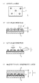
- FIG. 1 is a process explanatory view of the manufacturing method of the anisotropic conductive film of an example.
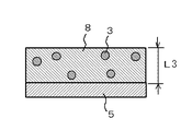
- FIG. 2 is a cross-sectional view of an anisotropic conductive film of a comparative example.
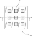
- FIG. 3A is a plan view of a transfer mold having a linear pattern that can be used in manufacturing an anisotropic conductive film.
- FIG. 3B is a plan view of a transfer mold having an island-shaped pattern that can be used when manufacturing an anisotropic conductive film.
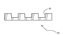
- 3C is a cross-sectional view taken along line AA of the transfer mold of FIGS. 3A and 3B.
- FIG. 4A is a process explanatory diagram of a method for producing an anisotropic conductive film using a transfer mold.
- FIG. 4A is a process explanatory diagram of a method for producing an anisotropic conductive film using a transfer mold.
- FIG. 4B is a process explanatory diagram of a method for producing an anisotropic conductive film using a transfer mold.
- FIG. 4C is a process explanatory diagram of a method for manufacturing an anisotropic conductive film using a transfer mold.
- FIG. 4D is a process explanatory diagram of a method for producing an anisotropic conductive film using a transfer mold.
- FIG. 4E is a process explanatory diagram of a method for producing an anisotropic conductive film using a transfer mold.
- FIG. 1 is a process explanatory diagram of a method for producing an anisotropic conductive film according to an embodiment of the present invention. Below, it demonstrates for every process.
- a particle dispersion 1 in which conductive particles 3 are dispersed in a thermoplastic resin diluent 2 that forms a film by drying is prepared. .
- the conductive particles 3 can be, for example, conductive particles used in known anisotropic conductive films, and metal-coated resin particles obtained by plating a resin core with nickel or gold, Examples thereof include metal particles such as nickel, cobalt, gold, silver, copper, and palladium, and these can be used alone or in combination.
- the size of the conductive particles 3 is preferably a spherical particle having a particle size of 0.2 to 5 ⁇ m, or a flaky particle having a thickness of 0.2 to 0.4 ⁇ m and a diameter of 1 to 10 ⁇ m.
- the particle size is preferably 1 to 20 ⁇ m, more preferably 3 to 10 ⁇ m, and the shape may be spherical, flake, rugby ball, or the like.
- the blending amount of the conductive particles 3 in the particle dispersion 1 is preferably 1 to 20 wt%.
- the blending amount is too small, the particle capture rate is lowered, and it is difficult to reliably connect the terminals.
- the thermoplastic resin diluent 2 contains a thermoplastic resin and a solvent.
- the thermoplastic resin is swollen, dissolved or suspended.
- a resin that can be easily deposited by drying the solvent to form a film and that can easily coat the conductive particles 3 is preferable.
- the thermoplastic resin has a softening point of 50 to 90 ° C. and flows by heating at the time of connection between terminals from the viewpoint of ensuring conductivity when connecting terminals with an anisotropic conductive film. Those having properties are preferred.
- examples of such a thermoplastic resin include an ethylene / vinyl acetate copolymer resin (EVA), a polyolefin resin, a polystyrene resin, and an acrylate resin. EVA is preferred.
- the solvent used for the thermoplastic resin diluent 2 it is preferable to contain a poor solvent for the thermoplastic resin so that the dried film can be easily formed by drying the coating film of the thermoplastic resin diluent 2. More specifically, although depending on the type of the thermoplastic resin, a mixture of a good solvent such as toluene or MEK and a poor solvent such as ethanol or IPA can be used.
- the solid content concentration of the thermoplastic resin in the thermoplastic resin diluent 2 can be appropriately set in order to make the distance between the conductive particles in the anisotropic conductive film a predetermined size.
- the inter-particle distance L2 (FIG. 1 (c)) of the coated conductive particles 4 in which the conductive particles 3 are coated with the dry coating 6b of the thermoplastic resin is used to ensure insulation. Therefore, 0.5 to 10 ⁇ m is preferable, and 1 to 6 ⁇ m is more preferable. Therefore, the solid content concentration of the thermoplastic resin in the thermoplastic resin diluent 2 is preferably 0.1 to 30 wt%, more preferably 2 to 15 wt%. .
- the interparticle distance L2 of the coated conductive particles 4 tends to increase as the concentration increases. Therefore, the interparticle distance L2 of the coated conductive particles 4 can be controlled by adjusting the concentration of the conductive particles 3 in the thermoplastic resin diluent 2.
- a method for preparing the particle dispersion 1 first, a solution of a thermoplastic resin is prepared, and a dispersion in which the conductive particles 3 are dispersed in a poor solvent for the thermoplastic resin is obtained. It is preferable to gradually add and disperse the solution.
- a thermoplastic resin diluent is first obtained and then conductive particles are dispersed in this diluent, the conductive particles are aggregated.
- the “aggregated state” refers to an aggregate in which the distance between the individual particles is appropriately maintained, and the present invention is a state in which each particle is in a non-contact and distanced group. Including things.
- a particle dispersion may be prepared by dispersing conductive particles in a solvent and blending the dispersion with a thermoplastic resin that forms a film by drying.
- the above-mentioned particle dispersion 1 is applied to a peeling substrate 5 such as PET film, PEN (polyethylene naphthalate), OPP (biaxially stretched polypropylene film) (FIG. 1B).
- a peeling substrate 5 such as PET film, PEN (polyethylene naphthalate), OPP (biaxially stretched polypropylene film) (FIG. 1B).
- the coating method it is preferable to apply the coating method using a bar coater, a roll coater or the like so that the coated conductive particles do not overlap in the thickness direction of the coating film, and the coated conductive particles form a single layer.
- the coating amount is preferably 1 to 10 ⁇ m and more preferably 1 to 7 ⁇ m as the thickness L1 of the coating film where the conductive particles 3 are present from the viewpoint of drying and film formation.
- the particle dispersion 1 when the particle dispersion 1 is applied to the release substrate 5, another release film is laminated on the coating film of the particle dispersion 1 to expand the coating film, and the particle coating has a disk shape or the like. By becoming an anisotropic shape, the movement of the conductive particles in the planar direction can be suppressed. This other release film can be peeled off after the coating film is expanded.
- the coating film of the particle dispersion 1 on the peeling substrate 5 is dried.
- the coated conductive particles 4 in which the conductive particles 3 are coated with the dried coating film 6a of the thermoplastic resin diluent on the dried coating film 6a of the thermoplastic resin diluent on the release substrate 5 are coated with each other.
- a conductive particle-containing layer 7 fixed as a single layer that does not overlap in the thickness direction of the film is formed ((c) in the figure).
- the coated conductive particles 4 are uniformly dispersed on the dried coating film 6a of the thermoplastic resin diluent, and the variation in the distance between the particles is remarkably suppressed.
- the drying temperature of the coating film of the particle dispersion 1 is preferably higher than the softening point of the thermoplastic resin and lower than the boiling point of the solvent.
- the coated conductive particles 4 can be fused to the dried coating film 6 a of the thermoplastic resin diluent on the peeling substrate 5, and the coated conductive particles 4 are uniformly dispersed in the conductive particle-containing layer 7. The state can be stabilized.
- the insulating resin layer 8 can be formed from an insulating resin layer-forming paint containing a film-forming resin, a curing component, a curing agent and the like used in known anisotropic conductive films. Moreover, as the insulating resin layer 8, what has tackiness is preferable. In addition, it is preferable that the coating of the coated conductive particles also contributes to tackiness. In this case, in order to contribute, a small amount of a solvent or a high affinity monomer may be left or mixed.
- examples of the film-forming resin include phenoxy resin, epoxy resin, unsaturated polyester resin, saturated polyester resin, urethane resin, butadiene resin, polyimide resin, polyamide resin, and polyolefin resin. More than one species can be used in combination. Among these, a phenoxy resin can be preferably used from the viewpoint of film forming property, workability, and connection reliability.
- examples of the curing component include liquid epoxy compounds and acrylic monomers.
- examples of the liquid epoxy compound include a bisphenol A type epoxy compound, a bisphenol F type epoxy compound, a novolac type epoxy compound, a modified epoxy compound thereof, an alicyclic epoxy compound, and the like.
- examples of the curing agent include thermal or photoanionic curing agents such as polyamine and imidazole, thermal or photocationic curing agents such as sulfonium salts, and thermal or photolatent curing agents such as phenolic curing agents. it can.
- examples of the acrylic monomer include ethyl (meth) acrylate.
- examples of the curing agent include organic peroxides and azobisisobutyronitrile.
- an insulating resin film is prepared in advance, and is laminated on the conductive particle-containing layer 7.
- the insulating resin film for example, the above-mentioned (i) film-forming resin, (ii) a curing component exhibiting tackiness, and (iii) a coating agent for forming an insulating resin layer containing a curing agent for the curing component It is possible to use a coating film formed by using and curing the coating film.
- the manufacturing method B of the anisotropic conductive film of this invention is produced by forming the conductive particle-containing layer using a transfer mold having a regular pattern, for example, transfer molds 30A and 30B as shown in FIG. 3A or 3B. You can also. It is easy to secure the distance between particles, and it is possible to widen the distance pitch between particles.
- FIG. 3A is a plan view of the transfer mold 30A in which the linear grooves 31 are formed
- FIG. 3B is a plan view of the transfer mold 30B in which square island-shaped recesses 32 are formed.
- the shape of the groove 31 or the recess 32 in the AA cross section of these transfer molds is, for example, a width on one side of the transfer mold 40 (the transfer molds 3A and 3B are collectively referred to as the transfer mold 40). It has a rectangular shape (hereinafter referred to as a recess 41) having a depth of 5 to 200 ⁇ m and a depth of 5 to 40 ⁇ m.
- a conductive particle group is composed of a plurality of conductive particles, and such a conductive particle group is linear, island-shaped, It is desirable to form in a discontinuous independent pattern shape such as a dot shape. Moreover, this shape is not limited to a straight line.
- the shortest distance in the pattern shape may be a space where one or two coating particles can exist. This is because, in a space where only one coating particle enters, the appearance frequency of a missing region where no particle exists is increased. Using the pattern in this way effectively works to improve reliability in securing a reliable insulating region. Also, from the viewpoint of production, the use of the pattern makes it easy to perform the inspection itself, and the defect extraction facilitates the merit of improving the quality.
- a particle dispersion 1 in which conductive particles 3 are dispersed in a thermoplastic resin diluent 2 that forms a film by drying is prepared. .
- a coating film of the particle dispersion 1 having a predetermined thickness is formed on the transfer mold 40, and the particle dispersion 1 on the surface of the transfer mold 40 is scraped off with a known wiper (FIG. 4A).
- a known wiper FIG. 4A
- the thermoplastic resin diluent 2 in which the conductive particles 3 are dispersed in the recess 41 is filled.
- the number of the conductive particles 3 entering the recess 41 varies depending on the size of the conductive particle 3, the width and depth of the recess 41, the concentration of the conductive particles 3 in the particle dispersion, and the like.
- the conductive particles 3 are filled with a single layer to form a conductive particle group 43.
- the manufacturing method C of the anisotropic conductive film of this invention can further take various aspects.
- the insulating resin layer 8 is formed in advance, and the particle dispersion 1 is applied on the insulating resin layer 8 and dried to form the conductive particle-containing layer 7. It may be formed.
- stacked can be obtained, without using the peeling base material 5.
- the insulating resin layer-forming coating material is directly applied to the conductive particle-containing layer 7 and dried or cured to make anisotropy.
- the conductive film 10 may be manufactured.
- the anisotropic conductive film of the present invention includes a first electronic component (for example, a mounting component such as an IC chip or an IC module) and a second electronic component (for example, a substrate such as a flexible substrate or a glass substrate). It can be preferably applied when anisotropic conductive connection is made.
- a first electronic component for example, a mounting component such as an IC chip or an IC module
- a second electronic component for example, a substrate such as a flexible substrate or a glass substrate. It can be preferably applied when anisotropic conductive connection is made.
- the anisotropic conductive film is temporarily attached to the second electronic component, the first electronic component is temporarily installed on the anisotropic conductive film temporarily attached to the second electronic component, and then the first
- the electronic component, the anisotropic conductive film, and the second electronic component are preferably heat-pressed or light-irradiated, and more preferably, heat-pressing is performed on the first electronic component or light-irradiated. This is done from under the second electronic component.
- These heating and pressurization and light irradiation can be performed simultaneously, but light irradiation can also be performed with a delay after the start of heating and pressurization.
- the present invention also includes a connection method using the anisotropic conductive film of the present invention and a connection body between the first electronic component and the second electronic component obtained by this connection method.
- the conductive particles 3 are randomly dispersed in a plurality of layers in the insulating resin layer 8 on the PET film 5, and the layer thickness L3 is 20 ⁇ m. It is.
- FIG. 3A (2) Formation of coated conductive particle group pattern FIG. 3A (Examples 6 to 8) in which the particle dispersion obtained in (1) has a pattern width (groove width or recess width) shown in Table 1 at a depth of 10 ⁇ m. Or the particle
- Table 1 shows the inter-particle distance L2 (see FIG. 1C) of the conductive particles coated with EVA in the coated conductive particle group after drying.
- the thickness L1 of the coating film and the inter-particle distance L2 were measured and taken as the average values.
- the anisotropic conductive films of Examples 1 to 11 are anisotropic conductive films of Comparative Example 1 in which conductive particles are arranged in a single layer by a biaxial stretching method, or a plurality of layers of conductive particles randomly. It turns out that conduction
- the results of Examples 1 to 3 show that the interparticle distance between the conductive particles can be changed by changing the solid content concentration of EVA.
- the same results can be obtained for the short-circuit occurrence rate and the conduction resistance regardless of whether the curing system of the insulating resin is a radical system, an anion system, or a cation system. I understand.
- similar results were obtained for the short-circuit occurrence rate and the conduction resistance regardless of whether or not a linear pattern or island pattern transfer mold was used when manufacturing the anisotropic conductive film. It turns out that it is obtained. It can be seen that the conductive resistance value tends to decrease as the pattern width increases.
- L1 and L2 tend to increase slightly as compared to Example 2 in which no transfer mold is used. This is considered to be because it is easily affected by pressure.
Landscapes
- Engineering & Computer Science (AREA)
- Chemical & Material Sciences (AREA)
- Manufacturing & Machinery (AREA)
- Organic Chemistry (AREA)
- Microelectronics & Electronic Packaging (AREA)
- Materials Engineering (AREA)
- Life Sciences & Earth Sciences (AREA)
- Wood Science & Technology (AREA)
- Physics & Mathematics (AREA)
- Spectroscopy & Molecular Physics (AREA)
- Dispersion Chemistry (AREA)
- Health & Medical Sciences (AREA)
- Chemical Kinetics & Catalysis (AREA)
- Medicinal Chemistry (AREA)
- Polymers & Plastics (AREA)
- Non-Insulated Conductors (AREA)
- Manufacturing Of Electrical Connectors (AREA)
- Electric Connection Of Electric Components To Printed Circuits (AREA)
- Adhesive Tapes (AREA)
- Adhesives Or Adhesive Processes (AREA)
- Conductive Materials (AREA)
Description
第2の電子部品上に、上述の異方性導電フィルムを仮貼りし、
仮貼りした異方性導電フィルム上に第1の電子部品を仮設置し、
次いで、第1の電子部品と異方性導電フィルムと第2の電子部品とを加熱加圧する接続方法を提供し、この接続方法による第1の電子部品と第2の電子部品との接続体を提供する。
図1は、本発明の一実施例の異方性導電フィルムの製造方法の工程説明図である。以下に工程毎に説明する。
まず、図1(a)に示すように、この実施例では、まず、乾燥により被膜を形成する熱可塑性樹脂希釈液2中に、導電性粒子3が分散している粒子分散液1を調製する。
次に、剥離基材5上の粒子分散液1の塗膜を乾燥させる。これにより剥離基材5上の熱可塑性樹脂希釈液の乾燥塗膜6aに、その熱可塑性樹脂希釈液の乾燥被膜6bで導電性粒子3が被覆された被覆導電性粒子4が、粒子同士が塗膜の厚さ方向に重なり合わない単層で固着した導電性粒子含有層7が形成される(同図(c))。この導電性粒子含有層7においては、被覆導電性粒子4が熱可塑性樹脂希釈液の乾燥塗膜6a上に一様に分散し、それらの粒子間距離のばらつきが著しく抑制されたものとなる。
次に、導電性粒子含有層7上に絶縁性樹脂層8を積層することにより、導電性粒子含有層7と絶縁性樹脂層8が積層している実施例の異方性導電フィルム10を得ることができる(同図(d))。
本発明の異方性導電フィルムは、導電性粒子含有層を規則的なパターンを有する転写型、例えば、図3A又は図3Bに示すような転写型30A、30Bを用いて形成することで製造することもできる。粒子間距離の確保が容易となり、また、粒子間距離ピッチを広くすることが可能となる。
まず、図1(a)に示すように、この実施例でも、まず、乾燥により被膜を形成する熱可塑性樹脂希釈液2中に、導電性粒子3が分散している粒子分散液1を調製する。
転写型40上に、所定厚の粒子分散液1の塗膜を形成し、公知のワイパーで転写型40の表面上の粒子分散液1を掻き取る(図4A)。これにより、窪み41中に導電性粒子3が分散している熱可塑性樹脂希釈液2が充填される。窪み41中に入り込む導電性粒子3の数は、導電性粒子3のサイズ、窪み41の幅や深さ、粒子分散液中の導電性粒子3の濃度等に応じて異なるが、通常は複数の導電性粒子3が単層で充填され、導電性粒子群43が構成される。
次に、転写型40の窪み41形成面に剥離フィルム50を載せ押圧して(図4B)、被覆導電粒子群43を剥離フィルム50上に転写し(図4C)、乾燥させる。これにより剥離フィルム50上に、導電性粒子3が熱可塑性樹脂44で固定された線状又は島状の被覆導電性粒子群パターン45が形成される(図4D)。
次に、被覆導電性粒子群パターン45上に絶縁性樹脂層8を積層し、剥離フィルム50を取り去ることにより、被覆導電性粒子群パターン45と絶縁性樹脂層8とが積層している実施例の異方性導電フィルム46を得ることができる(図4E)。
本発明の異方性導電フィルムの製造方法は更に種々の態様をとることができる。例えば、導電性粒子含有層7の形成にあたり、予め絶縁性樹脂層8を形成しておき、その絶縁性樹脂層8上に粒子分散液1を塗布し、乾燥して導電性粒子含有層7を形成してもよい。これにより、剥離基材5を使用することなく、導電性粒子含有層7と絶縁性樹脂層8とが積層した異方性導電フィルム10を得ることができる。
本発明の異方性導電フィルムは、第1の電子部品(例えば、ICチップ、ICモジュールなどの実装部品)と、第2の電子部品(例えば、フレキシブル基板、ガラス基板などの基板類)とを異方性導電接続する際に好ましく適用することができる。この場合、第2の電子部品に異方性導電フィルムを仮貼りし、第2の電子部品上に仮貼りした異方性導電フィルム上に第1の電子部品を仮設置し、次いで、第1の電子部品と異方性導電フィルムと第2の電子部品とを加熱加圧もしくは光照射することが好ましく、より好ましくは、加熱加圧を第1の電子部品の上から行い、もしくは光照射を第2電子部品の下から行う。これらの加熱加圧と光照射とは同時に行うこともできるが、加熱加圧開始後、遅れて光照射を行うこともできる。
(1)粒子分散液の調製
導電性粒子として、平均粒子径4μmの樹脂コアNiAuメッキ粒子(積水化学工業株式会社、AUL704)を使用し、この導電性粒子1.5gをエタノール50mLに分散させた。一方、乾燥により被膜を形成する熱可塑性樹脂としてエチレン・酢酸ビニル共重合樹脂(EVA)(住友化学株式会社、エバテート、型番:D2045、ビカット軟化温度83℃)を使用し、EVAのトルエン溶液を表1に示すように3通りの固形分濃度で調製し(2wt%、8wt%、15wt%)、このEVAのトルエン溶液5mLを、上述の導電性粒子の分散液に滴下しながら超音波ホモジナイザーで10分間分散させ、粒子分散液を得た。
(1)で得た粒子分散液を、PETフィルムにバーコーターで、表1に示す、塗膜の厚さ(乾燥前)L1(図1(b)参照)に塗布し、100℃で3分間熱風乾燥させ、導電性粒子含有層を形成した。乾燥後の導電性粒子含有層における、EVAで被覆された導電性粒子の粒子間距離L2(図1(c)参照)を表1に示す。なお、乾燥前の粒子分散液の塗膜の厚さL1と、乾燥後の粒子間距離L2は、金属顕微鏡(倍率×100)を用いて、100μm角の任意の領域内における導電性粒子(N=20)について塗膜の厚さL1と粒子間距離L2を測定し、その平均値とした。
表1に示す絶縁性樹脂層の原料成分を混合し、それをPETフィルムにバーコーターで塗布し、70℃で5分熱風乾燥して絶縁性樹脂フィルムを作製し、この絶縁性樹脂フィルムを上述の導電性粒子含有層にラミネーター(ロール表面温度45℃)でラミネートし、PETフィルム上に、層厚L3(図1(d)参照)が20μmの異方性導電フィルム10を作製した(実施例1~5)。
(1)粒子分散液の調製
実施例1で調製したものと同じ粒子分散液を調製した。
(1)で得た粒子分散液を、深さ10μmで表1に示すパターン幅(溝巾又は凹部巾)を有する図3A(実施例6~8)又は図3の転写型にバーコーターで、表1に示す塗膜の厚さ(乾燥前)L1(図1(b)参照)となるように塗布し、更に、溝又は凹部に入らなかった粒子分散液をワイパーで除去した後、剥離PETフィルムに溝又は凹部に充填された粒子分散液を転写した。これを100℃で3分間熱風乾燥し、被覆導電性粒子群パターンを形成した。乾燥後の被覆導電性粒子群における、EVAで被覆された導電性粒子の粒子間距離L2(図1(c)参照)を表1に示す。なお、乾燥前の粒子分散液の塗膜の厚さL1と、乾燥後の粒子間距離L2は、金属顕微鏡(倍率×100)を用いて、100μm角の任意の領域内における導電性粒子(N=20)について塗膜の厚さL1と粒子間距離L2を測定し、その平均値とした。
表1に示す絶縁性樹脂層の原料成分を混合し、それをPETフィルムにバーコーターで塗布し、70℃で5分熱風乾燥して絶縁性樹脂フィルムを作製し、この絶縁性樹脂フィルムを上述の被覆導電性粒子群パターンにラミネーター(ロール表面温度45℃)でラミネートし、PETフィルム上に、層厚L3(図1(d)参照)が20μmの異方性導電フィルムを作製した(実施例6~11)。
(イ)ショート発生率
実施例及び比較例の各異方性導電フィルムをそれぞれ35mm×20mmにカットし、ITOガラス(t=0.7mm)に貼り付け、アライメント実装設備にて、IC(1.5mm×13mm、t=0.5mm、Au-plated bump 25μm×140μm、h=15μm、Bump間スペース7.5μm)を圧着した(圧着条件:180℃、70Mpa 5秒、緩衝材 ポリテトラフルオロエチレン t=50μm)。こうして得られた接続体を、85℃、85%RHで250時間保管し、保管の前後のショートの発生率を求めた。結果を表1に示す。実用上、100ppm以下であることが望ましい。ショート発生率は、「ショートの発生数/7.5μmスペース総数」で算出される。
実施例及び比較例の各異方性導電フィルムをそれぞれ35mm×24mmにカットし、ITOガラス(t=0.7mm)に貼り付け、アライメント実装設備にて、IC(1.8mm×20mm、t=0.5mm、Au-plated bump 30μm×85μm、h=15μm)を圧着した(圧着条件:180℃、70Mpa 5秒、緩衝材 ポリテトラフルオロエチレン t=50μm)。こうして得られた接続体を、85℃、85%RHで250時間保管し、保管の前後の導通抵抗を測定した。結果を表1に示す。実用上、10Ω以下であることが望ましい。導通抵抗は、ICのバンプとパネル電極との間の抵抗を測定した。

2 熱可塑性樹脂希釈液
3 導電性粒子
4 被覆導電性粒子
5 剥離基材又はPETフィルム
6a 剥離基材上の熱可塑性樹脂の乾燥塗膜
6b 導電性粒子を被覆している熱可塑性樹脂の乾燥被膜
7 導電性粒子含有層
8 絶縁性樹脂層
10、46 異方性導電フィルム
30A、30B、40 転写型
31 溝
32 凹部
41 窪み
43 導電性粒子群
44 熱可塑性樹脂
45 被覆導電性粒子群パターン
50 剥離フィルム
Claims (14)
- 乾燥により被膜を形成する熱可塑性樹脂希釈液中に導電性粒子が分散している粒子分散液の塗膜を乾燥させることにより、その乾燥塗膜に該熱可塑性樹脂希釈液の乾燥被膜で被覆された被覆導電性粒子が単層で固着している導電性粒子含有層を形成し、導電性粒子含有層を絶縁性樹脂層と積層する異方性導電フィルムの製造方法。
- 粒子分散液における熱可塑性樹脂の固形分濃度の調整により異方性導電フィルムにおける導電性粒子の間隔を制御する請求項1記載の異方性導電フィルムの製造方法。
- 粒子分散液における熱可塑性樹脂の固形分濃度を、熱可塑性樹脂希釈液の2~15wt%に調整することにより、被覆導電性粒子の粒子間距離を1~6μmに制御する請求項2記載の異方性導電フィルムの製造方法。
- 溶媒に導電性粒子を分散し、その分散液に、乾燥により被膜を形成する熱可塑性樹脂を配合して粒子分散液を調製する請求項1~3のいずれかに記載の異方性導電フィルムの製造方法。
- 熱可塑性樹脂が、エチレン・酢酸ビニル共重合樹脂である請求項4記載の異方性導電フィルムの製造方法。
- 導電性粒子含有層に絶縁性樹脂フィルムをラミネートすることにより、導電性粒子含有層を絶縁性樹脂層と積層する請求項1~5のいずれかに記載の異方性導電フィルムの製造方法。
- 導電性粒子含有層が、規則的なパターンを有する転写型を用いて形成する請求項1~6のいずれかに記載の製造方法。
- 熱可塑性樹脂希釈液の乾燥塗膜に、該熱可塑性樹脂希釈液の乾燥被膜で被覆された被覆導電性粒子が単層で固着されている導電性粒子含有層と、絶縁性樹脂層とが積層している異方性導電フィルム。
- 前記熱可塑性樹脂が、エチレン・酢酸ビニル共重合樹脂である請求項8記載の異方性導電フィルム。
- 被覆導電性粒子の粒子間距離が1~6μmである請求項8又は9に記載の異方性導電フィルム。
- 複数の導電性粒子が、規則的なパターンで導電性粒子群を形成している請求項8~10載のいずれかに記載の異方性導電フィルム。
- 第1の電子部品の端子と第2の電子部品の端子とを異方性導電フィルムを用いて異方性導電接続する接続方法であって、
第2の電子部品上に、請求項8~11のいずれかに記載の異方性導電フィルムを仮貼りし、
第2の電子部品上に仮貼りした異方性導電フィルム上に第1の電子部品を仮設置し、
次いで、第1の電子部品と異方性導電フィルムと第2の電子部品とを加熱加圧する接続方法。 - 第1の電子部品が実装部品であり、第2の電子部品が基板類であり、第1の電子部品と異方性導電フィルムと第2の電子部品の加熱加圧を、第1の電子部品の上から加熱ツールで行う請求項12記載の接続方法。
- 請求項12又は13に記載の接続方法により得られた第1の電子部品と第2の電子部品との接続体。
Priority Applications (8)
| Application Number | Priority Date | Filing Date | Title |
|---|---|---|---|
| CN201380044670.7A CN104541417B (zh) | 2012-08-29 | 2013-08-28 | 各向异性导电膜及其制备方法 |
| HK15105977.9A HK1205365B (en) | 2012-08-29 | 2013-08-28 | Anisotropic conductive film and production method therefor |
| KR1020197017590A KR20190073605A (ko) | 2012-08-29 | 2013-08-28 | 이방성 도전 필름 및 그 제조 방법 |
| KR1020217020176A KR20210082571A (ko) | 2012-08-29 | 2013-08-28 | 이방성 도전 필름 및 그 제조 방법 |
| US14/420,982 US10412837B2 (en) | 2012-08-29 | 2013-08-28 | Anisotropic conductive film and method of producing the same |
| KR1020177018236A KR20170081295A (ko) | 2012-08-29 | 2013-08-28 | 이방성 도전 필름 및 그 제조 방법 |
| KR1020187012207A KR20180049207A (ko) | 2012-08-29 | 2013-08-28 | 이방성 도전 필름 및 그 제조 방법 |
| KR1020147033239A KR101843226B1 (ko) | 2012-08-29 | 2013-08-28 | 이방성 도전 필름 및 그 제조 방법 |
Applications Claiming Priority (2)
| Application Number | Priority Date | Filing Date | Title |
|---|---|---|---|
| JP2012188608 | 2012-08-29 | ||
| JP2012-188608 | 2012-08-29 |
Publications (1)
| Publication Number | Publication Date |
|---|---|
| WO2014034741A1 true WO2014034741A1 (ja) | 2014-03-06 |
Family
ID=50183547
Family Applications (1)
| Application Number | Title | Priority Date | Filing Date |
|---|---|---|---|
| PCT/JP2013/073053 Ceased WO2014034741A1 (ja) | 2012-08-29 | 2013-08-28 | 異方性導電フィルム及びその製造方法 |
Country Status (6)
| Country | Link |
|---|---|
| US (1) | US10412837B2 (ja) |
| JP (4) | JP6024623B2 (ja) |
| KR (5) | KR20170081295A (ja) |
| CN (2) | CN104541417B (ja) |
| TW (3) | TWI649764B (ja) |
| WO (1) | WO2014034741A1 (ja) |
Cited By (8)
| Publication number | Priority date | Publication date | Assignee | Title |
|---|---|---|---|---|
| WO2016068166A1 (ja) * | 2014-10-28 | 2016-05-06 | デクセリアルズ株式会社 | エンボスフィルム、枚葉フィルム、転写物、およびエンボスフィルムの製造方法 |
| JP2016084471A (ja) * | 2014-10-28 | 2016-05-19 | デクセリアルズ株式会社 | エンボスフィルム、枚葉フィルム、転写物、およびエンボスフィルムの製造方法 |
| WO2016080379A1 (ja) * | 2014-11-17 | 2016-05-26 | デクセリアルズ株式会社 | 異方性導電フィルム |
| WO2016190432A1 (ja) * | 2015-05-27 | 2016-12-01 | デクセリアルズ株式会社 | 異方導電性フィルム及び接続構造体 |
| US20190103201A1 (en) * | 2016-05-02 | 2019-04-04 | Dexerials Corporation | Method for manufacturing anisotropic conductive film, and anisotropic conductive film |
| JP2020084168A (ja) * | 2018-11-21 | 2020-06-04 | 信越化学工業株式会社 | 異方性フィルム |
| JP2020202409A (ja) * | 2015-01-13 | 2020-12-17 | デクセリアルズ株式会社 | 多層基板 |
| US12521919B2 (en) | 2018-11-21 | 2026-01-13 | Shin-Etsu Chemical Co., Ltd. | Anisotropic film and method for manufacturing anisotropic film |
Families Citing this family (20)
| Publication number | Priority date | Publication date | Assignee | Title |
|---|---|---|---|---|
| KR20170081295A (ko) | 2012-08-29 | 2017-07-11 | 데쿠세리아루즈 가부시키가이샤 | 이방성 도전 필름 및 그 제조 방법 |
| CN105940564B (zh) * | 2014-02-04 | 2020-03-24 | 迪睿合株式会社 | 各向异性导电膜及其制造方法 |
| JP6476747B2 (ja) * | 2014-10-28 | 2019-03-06 | デクセリアルズ株式会社 | 異方性導電フィルム及び接続構造体 |
| KR102240963B1 (ko) * | 2014-10-28 | 2021-04-16 | 데쿠세리아루즈 가부시키가이샤 | 이방성 도전 필름, 그 제조 방법, 및 접속 구조체 |
| WO2016114293A1 (ja) | 2015-01-13 | 2016-07-21 | デクセリアルズ株式会社 | バンプ形成用フィルム、半導体装置及びその製造方法、並びに接続構造体 |
| JP6661997B2 (ja) * | 2015-11-26 | 2020-03-11 | デクセリアルズ株式会社 | 異方性導電フィルム |
| WO2017191781A1 (ja) * | 2016-05-05 | 2017-11-09 | デクセリアルズ株式会社 | 異方性導電フィルム |
| JP7274811B2 (ja) * | 2016-05-05 | 2023-05-17 | デクセリアルズ株式会社 | 異方性導電フィルム |
| JP6907490B2 (ja) * | 2016-09-16 | 2021-07-21 | 昭和電工マテリアルズ株式会社 | 接続構造体及びその製造方法、端子付き電極の製造方法並びにこれに用いられる導電粒子、キット及び転写型 |
| KR102842615B1 (ko) * | 2016-10-03 | 2025-08-05 | 가부시끼가이샤 레조낙 | 도전성 필름, 권회체, 접속 구조체 및 접속 구조체의 제조 방법 |
| WO2018079365A1 (ja) * | 2016-10-24 | 2018-05-03 | デクセリアルズ株式会社 | 異方性導電フィルム |
| TWI763750B (zh) * | 2016-12-01 | 2022-05-11 | 日商迪睿合股份有限公司 | 異向性導電膜 |
| KR102794873B1 (ko) * | 2017-09-11 | 2025-04-11 | 가부시끼가이샤 레조낙 | 회로 접속용 접착제 필름 및 그의 제조 방법, 회로 접속 구조체의 제조 방법, 그리고 접착제 필름 수용 세트 |
| KR102254467B1 (ko) * | 2018-07-12 | 2021-05-21 | 에이치엔에스하이텍(주) | 이방도전성 접착필름의 제조방법 |
| KR102254470B1 (ko) * | 2018-07-12 | 2021-05-21 | 에이치엔에스하이텍(주) | 도전입자의 이격거리가 제어된 이방도전성 접착필름의 제조방법 |
| US20200156291A1 (en) * | 2018-11-21 | 2020-05-21 | Shin-Etsu Chemical Co., Ltd. | Anisotropic film and method for manufacturing anisotropic film |
| JP2020087907A (ja) * | 2018-11-21 | 2020-06-04 | 信越化学工業株式会社 | 異方性フィルムの製造方法 |
| KR102354305B1 (ko) | 2019-06-20 | 2022-01-21 | 주식회사 포스코 | 열전도-전기절연성 도료 조성물 및 이를 포함하는 태양전지용 외장재 강판 |
| US12520425B2 (en) * | 2020-04-30 | 2026-01-06 | Dujud Llc | Three-dimensional circuits with flexible interconnects |
| KR102336112B1 (ko) * | 2020-05-13 | 2021-12-07 | 한국과학기술원 | 균일 분산 및 수직 적층된 도전 입자를 함유하는 다층 폴리머 필름의 제조 방법 |
Citations (5)
| Publication number | Priority date | Publication date | Assignee | Title |
|---|---|---|---|---|
| JPH07302668A (ja) * | 1994-05-10 | 1995-11-14 | Hitachi Chem Co Ltd | 異方導電性樹脂フィルム状成形物の製法 |
| JP2007115560A (ja) * | 2005-10-21 | 2007-05-10 | Sumitomo Bakelite Co Ltd | 異方導電フィルム及びその製造方法 |
| WO2009037964A1 (ja) * | 2007-09-20 | 2009-03-26 | Sony Chemical & Information Device Corporation | 異方性導電膜及びその製造方法、並びに、該異方性導電膜を用いた接合体 |
| JP2010033793A (ja) * | 2008-07-28 | 2010-02-12 | Tokai Rubber Ind Ltd | 粒子転写膜の製造方法 |
| WO2011040458A1 (ja) * | 2009-09-30 | 2011-04-07 | ソニーケミカル&インフォメーションデバイス株式会社 | 異方性導電フィルム及びその製造方法 |
Family Cites Families (22)
| Publication number | Priority date | Publication date | Assignee | Title |
|---|---|---|---|---|
| JPH0622084B2 (ja) | 1988-10-18 | 1994-03-23 | スタンレー電気株式会社 | 電極端子転移用異方性導電膜の形成方法 |
| JP2748713B2 (ja) | 1991-03-29 | 1998-05-13 | 日立化成工業株式会社 | 接続部材 |
| TW277152B (ja) | 1994-05-10 | 1996-06-01 | Hitachi Chemical Co Ltd | |
| JPH09118860A (ja) * | 1995-08-22 | 1997-05-06 | Bridgestone Corp | 異方性導電フィルム |
| US20010008169A1 (en) | 1998-06-30 | 2001-07-19 | 3M Innovative Properties Company | Fine pitch anisotropic conductive adhesive |
| CN100437838C (zh) * | 2003-07-07 | 2008-11-26 | 积水化学工业株式会社 | 包覆导电性粒子、各向异性导电材料以及导电连接结构体 |
| CN1906705B (zh) * | 2004-01-30 | 2010-04-21 | 积水化学工业株式会社 | 导电性微粒和各向异性导电材料 |
| JP2006278014A (ja) * | 2005-03-28 | 2006-10-12 | Three M Innovative Properties Co | 異方導電性構造体 |
| KR101359065B1 (ko) * | 2006-04-11 | 2014-02-05 | 제이에스알 가부시끼가이샤 | 이방 도전성 커넥터 및 이방 도전성 커넥터 장치 |
| WO2007125993A1 (ja) | 2006-04-27 | 2007-11-08 | Asahi Kasei Emd Corporation | 導電粒子配置シート及び異方導電性フィルム |
| JP4789738B2 (ja) * | 2006-07-28 | 2011-10-12 | 旭化成イーマテリアルズ株式会社 | 異方導電性フィルム |
| JP5186157B2 (ja) * | 2007-08-24 | 2013-04-17 | デクセリアルズ株式会社 | 異方性導電フィルム及びそれを用いた接続構造体の製造方法 |
| JP5225766B2 (ja) | 2008-06-25 | 2013-07-03 | 旭化成イーマテリアルズ株式会社 | 異方導電性接着シート及び微細接続構造体 |
| PH12012500652A1 (en) * | 2009-09-30 | 2012-10-22 | Sumitomo Bakelite Co | Conductive connecting material, method for connecting terminals and method for producing connection terminal |
| KR20120076187A (ko) * | 2010-12-29 | 2012-07-09 | 제일모직주식회사 | 이방 도전성 필름 |
| KR20170081295A (ko) | 2012-08-29 | 2017-07-11 | 데쿠세리아루즈 가부시키가이샤 | 이방성 도전 필름 및 그 제조 방법 |
| JP5972844B2 (ja) * | 2012-09-18 | 2016-08-17 | デクセリアルズ株式会社 | 異方性導電フィルム、異方性導電フィルムの製造方法、接続体の製造方法、及び接続方法 |
| KR101330961B1 (ko) * | 2012-12-26 | 2013-11-18 | 신한카드 주식회사 | 모바일 신용카드의 발급처리 방법 |
| JP5695768B2 (ja) | 2014-02-04 | 2015-04-08 | 日本化学工業株式会社 | 導電性粉体及びそれを含む導電性材料 |
| CN105940563B (zh) * | 2014-02-04 | 2019-03-05 | 迪睿合株式会社 | 各向异性导电膜及其制造方法 |
| JP6661969B2 (ja) * | 2014-10-28 | 2020-03-11 | デクセリアルズ株式会社 | 異方性導電フィルム及び接続構造体 |
| TWI785642B (zh) | 2014-11-17 | 2022-12-01 | 日商迪睿合股份有限公司 | 異向性導電膜及連接構造體 |
-
2013
- 2013-08-28 KR KR1020177018236A patent/KR20170081295A/ko not_active Ceased
- 2013-08-28 KR KR1020187012207A patent/KR20180049207A/ko not_active Ceased
- 2013-08-28 KR KR1020147033239A patent/KR101843226B1/ko active Active
- 2013-08-28 US US14/420,982 patent/US10412837B2/en active Active
- 2013-08-28 CN CN201380044670.7A patent/CN104541417B/zh active Active
- 2013-08-28 WO PCT/JP2013/073053 patent/WO2014034741A1/ja not_active Ceased
- 2013-08-28 KR KR1020217020176A patent/KR20210082571A/ko not_active Ceased
- 2013-08-28 JP JP2013177080A patent/JP6024623B2/ja active Active
- 2013-08-28 KR KR1020197017590A patent/KR20190073605A/ko not_active Ceased
- 2013-08-28 CN CN201710384614.8A patent/CN107189562B/zh active Active
- 2013-08-29 TW TW106115306A patent/TWI649764B/zh active
- 2013-08-29 TW TW102131011A patent/TWI604467B/zh active
- 2013-08-29 TW TW107134663A patent/TWI661435B/zh active
-
2016
- 2016-10-07 JP JP2016198884A patent/JP2017017039A/ja active Pending
-
2018
- 2018-06-26 JP JP2018121397A patent/JP2018186090A/ja active Pending
-
2019
- 2019-12-10 JP JP2019222847A patent/JP2020057611A/ja active Pending
Patent Citations (5)
| Publication number | Priority date | Publication date | Assignee | Title |
|---|---|---|---|---|
| JPH07302668A (ja) * | 1994-05-10 | 1995-11-14 | Hitachi Chem Co Ltd | 異方導電性樹脂フィルム状成形物の製法 |
| JP2007115560A (ja) * | 2005-10-21 | 2007-05-10 | Sumitomo Bakelite Co Ltd | 異方導電フィルム及びその製造方法 |
| WO2009037964A1 (ja) * | 2007-09-20 | 2009-03-26 | Sony Chemical & Information Device Corporation | 異方性導電膜及びその製造方法、並びに、該異方性導電膜を用いた接合体 |
| JP2010033793A (ja) * | 2008-07-28 | 2010-02-12 | Tokai Rubber Ind Ltd | 粒子転写膜の製造方法 |
| WO2011040458A1 (ja) * | 2009-09-30 | 2011-04-07 | ソニーケミカル&インフォメーションデバイス株式会社 | 異方性導電フィルム及びその製造方法 |
Cited By (39)
| Publication number | Priority date | Publication date | Assignee | Title |
|---|---|---|---|---|
| CN107073806B (zh) * | 2014-10-28 | 2019-09-06 | 迪睿合株式会社 | 压花膜、片状膜、转印物以及压花膜的制造方法 |
| JP2016084471A (ja) * | 2014-10-28 | 2016-05-19 | デクセリアルズ株式会社 | エンボスフィルム、枚葉フィルム、転写物、およびエンボスフィルムの製造方法 |
| US10890844B2 (en) | 2014-10-28 | 2021-01-12 | Dexerials Corporation | Embossed film, sheet film, transfer copy, and method for producing embossed film |
| WO2016068166A1 (ja) * | 2014-10-28 | 2016-05-06 | デクセリアルズ株式会社 | エンボスフィルム、枚葉フィルム、転写物、およびエンボスフィルムの製造方法 |
| JP2020114680A (ja) * | 2014-10-28 | 2020-07-30 | デクセリアルズ株式会社 | エンボスフィルム、枚葉フィルム、転写物、およびエンボスフィルムの製造方法 |
| CN107073806A (zh) * | 2014-10-28 | 2017-08-18 | 迪睿合株式会社 | 压花膜、片状膜、转印物以及压花膜的制造方法 |
| JP2022060302A (ja) * | 2014-10-28 | 2022-04-14 | デクセリアルズ株式会社 | エンボスフィルム、枚葉フィルム、転写物、およびエンボスフィルムの製造方法 |
| US11543746B2 (en) | 2014-10-28 | 2023-01-03 | Dexerials Corporation | Embossed film, sheet film, transfer copy, and method for producing embossed film |
| US10245780B2 (en) | 2014-10-28 | 2019-04-02 | Dexerials Corporation | Embossed film, sheet film, transfer copy, and method for producing embossed film |
| US10304796B2 (en) | 2014-11-17 | 2019-05-28 | Dexerials Corporation | Anisotropic electrically conductive film having electrically conductive particles disposed in a lattice point region of a planar lattice pattern |
| CN112421263A (zh) * | 2014-11-17 | 2021-02-26 | 迪睿合株式会社 | 各向异性导电膜、连接结构体及其制造方法 |
| CN114512832B (zh) * | 2014-11-17 | 2024-03-01 | 迪睿合株式会社 | 各向异性导电膜及其制造方法、连接结构体 |
| US10026709B2 (en) | 2014-11-17 | 2018-07-17 | Dexerials Corporation | Anisotropic electrically conductive film |
| CN114512832A (zh) * | 2014-11-17 | 2022-05-17 | 迪睿合株式会社 | 各向异性导电膜及其制造方法、连接结构体 |
| CN111029875A (zh) * | 2014-11-17 | 2020-04-17 | 迪睿合株式会社 | 各向异性导电膜、连接结构体及其制造方法 |
| CN111029875B (zh) * | 2014-11-17 | 2022-05-10 | 迪睿合株式会社 | 各向异性导电膜、连接结构体及其制造方法 |
| CN107078420A (zh) * | 2014-11-17 | 2017-08-18 | 迪睿合株式会社 | 各向异性导电膜 |
| US11923333B2 (en) | 2014-11-17 | 2024-03-05 | Dexerials Corporation | Anisotropic electrically conductive film |
| US12087722B2 (en) * | 2014-11-17 | 2024-09-10 | Dexerials Corporation | Anisotropic electrically conductive film |
| WO2016080379A1 (ja) * | 2014-11-17 | 2016-05-26 | デクセリアルズ株式会社 | 異方性導電フィルム |
| CN112421262A (zh) * | 2014-11-17 | 2021-02-26 | 迪睿合株式会社 | 各向异性导电膜、连接结构体及其制造方法 |
| JP2020202409A (ja) * | 2015-01-13 | 2020-12-17 | デクセリアルズ株式会社 | 多層基板 |
| JP7207382B2 (ja) | 2015-01-13 | 2023-01-18 | デクセリアルズ株式会社 | 多層基板 |
| US20200161268A1 (en) * | 2015-05-27 | 2020-05-21 | Dexerials Corporation | Anisotropic electrically conductive film and connection structure |
| JP7356046B2 (ja) | 2015-05-27 | 2023-10-04 | デクセリアルズ株式会社 | 異方導電性フィルム及び接続構造体 |
| WO2016190432A1 (ja) * | 2015-05-27 | 2016-12-01 | デクセリアルズ株式会社 | 異方導電性フィルム及び接続構造体 |
| US10892243B2 (en) | 2015-05-27 | 2021-01-12 | Dexerials Corporation | Anisotropic electrically conductive film and connection structure |
| US10546831B2 (en) | 2015-05-27 | 2020-01-28 | Dexerials Corporation | Anisotropic electrically conductive film and connection structure |
| KR102449287B1 (ko) * | 2015-05-27 | 2022-09-29 | 데쿠세리아루즈 가부시키가이샤 | 이방 도전성 필름 및 접속 구조체 |
| JP2022043193A (ja) * | 2015-05-27 | 2022-03-15 | デクセリアルズ株式会社 | 異方導電性フィルム及び接続構造体 |
| JP2016225296A (ja) * | 2015-05-27 | 2016-12-28 | デクセリアルズ株式会社 | 異方導電性フィルム及び接続構造体 |
| JP7233156B2 (ja) | 2015-05-27 | 2023-03-06 | デクセリアルズ株式会社 | 異方導電性フィルム及び接続構造体 |
| KR20190126456A (ko) * | 2015-05-27 | 2019-11-11 | 데쿠세리아루즈 가부시키가이샤 | 이방 도전성 필름 및 접속 구조체 |
| US11004574B2 (en) * | 2016-05-02 | 2021-05-11 | Dexerials Corporation | Method for manufacturing anisotropic conductive film, and anisotropic conductive film |
| US20190103201A1 (en) * | 2016-05-02 | 2019-04-04 | Dexerials Corporation | Method for manufacturing anisotropic conductive film, and anisotropic conductive film |
| US12014840B2 (en) | 2016-05-02 | 2024-06-18 | Dexerials Corporation | Method for manufacturing anisotropic conductive film, and anisotropic conductive film |
| JP7240226B2 (ja) | 2018-11-21 | 2023-03-15 | 信越化学工業株式会社 | 異方性フィルム |
| JP2020084168A (ja) * | 2018-11-21 | 2020-06-04 | 信越化学工業株式会社 | 異方性フィルム |
| US12521919B2 (en) | 2018-11-21 | 2026-01-13 | Shin-Etsu Chemical Co., Ltd. | Anisotropic film and method for manufacturing anisotropic film |
Also Published As
| Publication number | Publication date |
|---|---|
| CN104541417A (zh) | 2015-04-22 |
| TW201905936A (zh) | 2019-02-01 |
| KR20170081295A (ko) | 2017-07-11 |
| JP2020057611A (ja) | 2020-04-09 |
| KR20180049207A (ko) | 2018-05-10 |
| KR20210082571A (ko) | 2021-07-05 |
| JP2017017039A (ja) | 2017-01-19 |
| TW201435919A (zh) | 2014-09-16 |
| TWI649764B (zh) | 2019-02-01 |
| JP2018186090A (ja) | 2018-11-22 |
| CN107189562A (zh) | 2017-09-22 |
| US20150319867A1 (en) | 2015-11-05 |
| KR101843226B1 (ko) | 2018-03-28 |
| TW201730896A (zh) | 2017-09-01 |
| CN104541417B (zh) | 2017-09-26 |
| KR20150048667A (ko) | 2015-05-07 |
| TWI661435B (zh) | 2019-06-01 |
| JP6024623B2 (ja) | 2016-11-16 |
| JP2014063729A (ja) | 2014-04-10 |
| TWI604467B (zh) | 2017-11-01 |
| KR20190073605A (ko) | 2019-06-26 |
| HK1205365A1 (en) | 2015-12-11 |
| CN107189562B (zh) | 2021-01-19 |
| US10412837B2 (en) | 2019-09-10 |
Similar Documents
| Publication | Publication Date | Title |
|---|---|---|
| JP6024623B2 (ja) | 異方性導電フィルム及びその製造方法 | |
| TW201606798A (zh) | 異向性導電膜及其製造方法 | |
| KR102326117B1 (ko) | 이방성 도전 필름, 그 제조 방법, 및 접속 구조체 | |
| TWI764821B (zh) | 異向性導電膜 | |
| WO2015056518A1 (ja) | 異方性導電フィルム | |
| TWI775562B (zh) | 異向性導電膜之製造方法、異向性導電膜、異向性導電膜捲裝體、連接構造體之製造方法、連接構造體、填料配置膜之製造方法、及填料配置膜 | |
| JP2015167186A (ja) | 接続構造体の製造方法及び接続構造体 | |
| JP2006032335A (ja) | 異方導電性接着フィルム | |
| TWI781213B (zh) | 異向性導電膜、連接結構體及彼等之製造方法 | |
| JP4175347B2 (ja) | 異方導電性接着フィルムの製造方法 | |
| HK1240608A1 (en) | Anisotropic conductive film and method of producing the same | |
| HK1240608B (en) | Anisotropic conductive film and method of producing the same | |
| HK1205365B (en) | Anisotropic conductive film and production method therefor | |
| JP2010007076A (ja) | 異方導電性接着フィルム | |
| JP2005325366A (ja) | 異方導電性接着フィルム | |
| CN108886227A (zh) | 各向异性导电膜的制造方法及各向异性导电膜 |
Legal Events
| Date | Code | Title | Description |
|---|---|---|---|
| 121 | Ep: the epo has been informed by wipo that ep was designated in this application |
Ref document number: 13832201 Country of ref document: EP Kind code of ref document: A1 |
|
| ENP | Entry into the national phase |
Ref document number: 20147033239 Country of ref document: KR Kind code of ref document: A |
|
| WWE | Wipo information: entry into national phase |
Ref document number: 14420982 Country of ref document: US |
|
| NENP | Non-entry into the national phase |
Ref country code: DE |
|
| 122 | Ep: pct application non-entry in european phase |
Ref document number: 13832201 Country of ref document: EP Kind code of ref document: A1 |