WO2014017568A1 - はんだ合金 - Google Patents
はんだ合金 Download PDFInfo
- Publication number
- WO2014017568A1 WO2014017568A1 PCT/JP2013/070122 JP2013070122W WO2014017568A1 WO 2014017568 A1 WO2014017568 A1 WO 2014017568A1 JP 2013070122 W JP2013070122 W JP 2013070122W WO 2014017568 A1 WO2014017568 A1 WO 2014017568A1
- Authority
- WO
- WIPO (PCT)
- Prior art keywords
- solder
- less
- oxide layer
- mass
- alloy
- Prior art date
- Legal status (The legal status is an assumption and is not a legal conclusion. Google has not performed a legal analysis and makes no representation as to the accuracy of the status listed.)
- Ceased
Links
Images

Classifications
-
- B—PERFORMING OPERATIONS; TRANSPORTING
- B23—MACHINE TOOLS; METAL-WORKING NOT OTHERWISE PROVIDED FOR
- B23K—SOLDERING OR UNSOLDERING; WELDING; CLADDING OR PLATING BY SOLDERING OR WELDING; CUTTING BY APPLYING HEAT LOCALLY, e.g. FLAME CUTTING; WORKING BY LASER BEAM
- B23K35/00—Rods, electrodes, materials, or media, for use in soldering, welding, or cutting
- B23K35/02—Rods, electrodes, materials, or media, for use in soldering, welding, or cutting characterised by mechanical features, e.g. shape
- B23K35/0222—Rods, electrodes, materials, or media, for use in soldering, welding, or cutting characterised by mechanical features, e.g. shape for use in soldering or brazing
-
- B—PERFORMING OPERATIONS; TRANSPORTING
- B23—MACHINE TOOLS; METAL-WORKING NOT OTHERWISE PROVIDED FOR
- B23K—SOLDERING OR UNSOLDERING; WELDING; CLADDING OR PLATING BY SOLDERING OR WELDING; CUTTING BY APPLYING HEAT LOCALLY, e.g. FLAME CUTTING; WORKING BY LASER BEAM
- B23K35/00—Rods, electrodes, materials, or media, for use in soldering, welding, or cutting
- B23K35/22—Rods, electrodes, materials, or media, for use in soldering, welding, or cutting characterised by the composition or nature of the material
- B23K35/24—Selection of soldering or welding materials proper
-
- B—PERFORMING OPERATIONS; TRANSPORTING
- B23—MACHINE TOOLS; METAL-WORKING NOT OTHERWISE PROVIDED FOR
- B23K—SOLDERING OR UNSOLDERING; WELDING; CLADDING OR PLATING BY SOLDERING OR WELDING; CUTTING BY APPLYING HEAT LOCALLY, e.g. FLAME CUTTING; WORKING BY LASER BEAM
- B23K35/00—Rods, electrodes, materials, or media, for use in soldering, welding, or cutting
- B23K35/22—Rods, electrodes, materials, or media, for use in soldering, welding, or cutting characterised by the composition or nature of the material
- B23K35/24—Selection of soldering or welding materials proper
- B23K35/26—Selection of soldering or welding materials proper with the principal constituent melting at less than 400°C
-
- B—PERFORMING OPERATIONS; TRANSPORTING
- B23—MACHINE TOOLS; METAL-WORKING NOT OTHERWISE PROVIDED FOR
- B23K—SOLDERING OR UNSOLDERING; WELDING; CLADDING OR PLATING BY SOLDERING OR WELDING; CUTTING BY APPLYING HEAT LOCALLY, e.g. FLAME CUTTING; WORKING BY LASER BEAM
- B23K35/00—Rods, electrodes, materials, or media, for use in soldering, welding, or cutting
- B23K35/22—Rods, electrodes, materials, or media, for use in soldering, welding, or cutting characterised by the composition or nature of the material
- B23K35/24—Selection of soldering or welding materials proper
- B23K35/26—Selection of soldering or welding materials proper with the principal constituent melting at less than 400°C
- B23K35/262—Sn as the principal constituent
-
- B—PERFORMING OPERATIONS; TRANSPORTING
- B23—MACHINE TOOLS; METAL-WORKING NOT OTHERWISE PROVIDED FOR
- B23K—SOLDERING OR UNSOLDERING; WELDING; CLADDING OR PLATING BY SOLDERING OR WELDING; CUTTING BY APPLYING HEAT LOCALLY, e.g. FLAME CUTTING; WORKING BY LASER BEAM
- B23K35/00—Rods, electrodes, materials, or media, for use in soldering, welding, or cutting
- B23K35/22—Rods, electrodes, materials, or media, for use in soldering, welding, or cutting characterised by the composition or nature of the material
- B23K35/24—Selection of soldering or welding materials proper
- B23K35/26—Selection of soldering or welding materials proper with the principal constituent melting at less than 400°C
- B23K35/264—Bi as the principal constituent
-
- B—PERFORMING OPERATIONS; TRANSPORTING
- B23—MACHINE TOOLS; METAL-WORKING NOT OTHERWISE PROVIDED FOR
- B23K—SOLDERING OR UNSOLDERING; WELDING; CLADDING OR PLATING BY SOLDERING OR WELDING; CUTTING BY APPLYING HEAT LOCALLY, e.g. FLAME CUTTING; WORKING BY LASER BEAM
- B23K35/00—Rods, electrodes, materials, or media, for use in soldering, welding, or cutting
- B23K35/22—Rods, electrodes, materials, or media, for use in soldering, welding, or cutting characterised by the composition or nature of the material
- B23K35/24—Selection of soldering or welding materials proper
- B23K35/26—Selection of soldering or welding materials proper with the principal constituent melting at less than 400°C
- B23K35/268—Pb as the principal constituent
-
- B—PERFORMING OPERATIONS; TRANSPORTING
- B23—MACHINE TOOLS; METAL-WORKING NOT OTHERWISE PROVIDED FOR
- B23K—SOLDERING OR UNSOLDERING; WELDING; CLADDING OR PLATING BY SOLDERING OR WELDING; CUTTING BY APPLYING HEAT LOCALLY, e.g. FLAME CUTTING; WORKING BY LASER BEAM
- B23K35/00—Rods, electrodes, materials, or media, for use in soldering, welding, or cutting
- B23K35/22—Rods, electrodes, materials, or media, for use in soldering, welding, or cutting characterised by the composition or nature of the material
- B23K35/24—Selection of soldering or welding materials proper
- B23K35/28—Selection of soldering or welding materials proper with the principal constituent melting at less than 950°C
- B23K35/282—Zn as the principal constituent
-
- B—PERFORMING OPERATIONS; TRANSPORTING
- B23—MACHINE TOOLS; METAL-WORKING NOT OTHERWISE PROVIDED FOR
- B23K—SOLDERING OR UNSOLDERING; WELDING; CLADDING OR PLATING BY SOLDERING OR WELDING; CUTTING BY APPLYING HEAT LOCALLY, e.g. FLAME CUTTING; WORKING BY LASER BEAM
- B23K35/00—Rods, electrodes, materials, or media, for use in soldering, welding, or cutting
- B23K35/22—Rods, electrodes, materials, or media, for use in soldering, welding, or cutting characterised by the composition or nature of the material
- B23K35/24—Selection of soldering or welding materials proper
- B23K35/30—Selection of soldering or welding materials proper with the principal constituent melting at less than 1550°C
- B23K35/3013—Au as the principal constituent
-
- B—PERFORMING OPERATIONS; TRANSPORTING
- B23—MACHINE TOOLS; METAL-WORKING NOT OTHERWISE PROVIDED FOR
- B23K—SOLDERING OR UNSOLDERING; WELDING; CLADDING OR PLATING BY SOLDERING OR WELDING; CUTTING BY APPLYING HEAT LOCALLY, e.g. FLAME CUTTING; WORKING BY LASER BEAM
- B23K35/00—Rods, electrodes, materials, or media, for use in soldering, welding, or cutting
- B23K35/40—Making wire or rods for soldering or welding
-
- C—CHEMISTRY; METALLURGY
- C22—METALLURGY; FERROUS OR NON-FERROUS ALLOYS; TREATMENT OF ALLOYS OR NON-FERROUS METALS
- C22C—ALLOYS
- C22C1/00—Making non-ferrous alloys
- C22C1/02—Making non-ferrous alloys by melting
-
- C—CHEMISTRY; METALLURGY
- C22—METALLURGY; FERROUS OR NON-FERROUS ALLOYS; TREATMENT OF ALLOYS OR NON-FERROUS METALS
- C22C—ALLOYS
- C22C11/00—Alloys based on lead
-
- C—CHEMISTRY; METALLURGY
- C22—METALLURGY; FERROUS OR NON-FERROUS ALLOYS; TREATMENT OF ALLOYS OR NON-FERROUS METALS
- C22C—ALLOYS
- C22C11/00—Alloys based on lead
- C22C11/04—Alloys based on lead with copper as the next major constituent
-
- C—CHEMISTRY; METALLURGY
- C22—METALLURGY; FERROUS OR NON-FERROUS ALLOYS; TREATMENT OF ALLOYS OR NON-FERROUS METALS
- C22C—ALLOYS
- C22C11/00—Alloys based on lead
- C22C11/06—Alloys based on lead with tin as the next major constituent
-
- C—CHEMISTRY; METALLURGY
- C22—METALLURGY; FERROUS OR NON-FERROUS ALLOYS; TREATMENT OF ALLOYS OR NON-FERROUS METALS
- C22C—ALLOYS
- C22C12/00—Alloys based on antimony or bismuth
-
- C—CHEMISTRY; METALLURGY
- C22—METALLURGY; FERROUS OR NON-FERROUS ALLOYS; TREATMENT OF ALLOYS OR NON-FERROUS METALS
- C22C—ALLOYS
- C22C13/00—Alloys based on tin
-
- C—CHEMISTRY; METALLURGY
- C22—METALLURGY; FERROUS OR NON-FERROUS ALLOYS; TREATMENT OF ALLOYS OR NON-FERROUS METALS
- C22C—ALLOYS
- C22C13/00—Alloys based on tin
- C22C13/02—Alloys based on tin with antimony or bismuth as the next major constituent
-
- C—CHEMISTRY; METALLURGY
- C22—METALLURGY; FERROUS OR NON-FERROUS ALLOYS; TREATMENT OF ALLOYS OR NON-FERROUS METALS
- C22C—ALLOYS
- C22C28/00—Alloys based on a metal not provided for in groups C22C5/00 - C22C27/00
-
- C—CHEMISTRY; METALLURGY
- C22—METALLURGY; FERROUS OR NON-FERROUS ALLOYS; TREATMENT OF ALLOYS OR NON-FERROUS METALS
- C22C—ALLOYS
- C22C5/00—Alloys based on noble metals
- C22C5/02—Alloys based on gold
-
- H—ELECTRICITY
- H05—ELECTRIC TECHNIQUES NOT OTHERWISE PROVIDED FOR
- H05K—PRINTED CIRCUITS; CASINGS OR CONSTRUCTIONAL DETAILS OF ELECTRIC APPARATUS; MANUFACTURE OF ASSEMBLAGES OF ELECTRICAL COMPONENTS
- H05K1/00—Printed circuits
- H05K1/18—Printed circuits structurally associated with non-printed electric components
-
- Y—GENERAL TAGGING OF NEW TECHNOLOGICAL DEVELOPMENTS; GENERAL TAGGING OF CROSS-SECTIONAL TECHNOLOGIES SPANNING OVER SEVERAL SECTIONS OF THE IPC; TECHNICAL SUBJECTS COVERED BY FORMER USPC CROSS-REFERENCE ART COLLECTIONS [XRACs] AND DIGESTS
- Y10—TECHNICAL SUBJECTS COVERED BY FORMER USPC
- Y10T—TECHNICAL SUBJECTS COVERED BY FORMER US CLASSIFICATION
- Y10T428/00—Stock material or miscellaneous articles
- Y10T428/24—Structurally defined web or sheet [e.g., overall dimension, etc.]
- Y10T428/24355—Continuous and nonuniform or irregular surface on layer or component [e.g., roofing, etc.]
Definitions
- the present invention relates to a solder alloy that is excellent in wettability and bondability, and thus has high bonding reliability.
- solder used for joining electronic parts In order to meet this requirement, it is necessary to have excellent wettability and bondability to a substrate or the like.
- the types of solder are roughly classified into Pb-based, Sn-based, Au-based, In-based, and the like, and various types are used depending on applications.
- any type of solder it is still necessary to satisfy the above requirements for wettability and bondability. Under such circumstances, various ideas have been made to improve wettability and the like, but there are still many problems.
- Patent Documents 1 and 2 in a solder alloy containing Sn as a main component and adding Cu as an oxidation-inhibiting element and Ag as a wettability improving element in a solder alloy containing Cu, wetting of the solder alloy It is described to improve the sex.
- Au plating is applied to a joint portion of a circuit board, an electronic component, etc., solder is heated and melted in a non-oxidizing or reducing atmosphere, and a new surface of the solder is exposed to ensure wettability.
- Patent Document 4 discloses that a mixture of a flux of Sn—Au alloy solder powder containing 6.5 to 9.8% by mass of Au and the balance being composed of Sn and inevitable impurities and flux. A characteristic Sn—Au alloy solder paste is described. This Sn—Au alloy solder paste is said to have excellent wettability and less voids.
- Patent Documents 1 and 2 do not specify the mechanism by which the oxidation-inhibiting element and the wettability improving element are effective.
- the oxidizing property (or reducing property) of Ge is almost the same as Sn, and it is difficult to think that Ge improves the wettability due to the redox phenomenon.
- P can be expected to reduce the solder and the like when the solder is melted, but P oxide is a gas, which may cause voids and poor bonding during bonding. Therefore, it is not possible to understand how P behaves and improves wettability in Sn—Cu based alloys in these patent documents.
- Patent Document 3 does not describe in detail the mechanism by which the new surface is exposed, the atmosphere control during bonding, and the like. Further, in the technique of Patent Document 3, the oxide film on the solder surface formed at the time of solder manufacture cannot be removed, and even if the new surface is exposed because the oxide film is broken or the like, the oxide on the solder surface is not separated from the circuit board and the electron. Since it remains between components, it is inevitable that voids are generated and the bonding strength is reduced. Patent Document 3 does not mention anything about such a problem, and high bonding reliability cannot be obtained in a bonding state in which the oxide on the solder surface remains between the circuit board and the electronic component. It can be said.
- Patent Document 4 does not specify a mechanism for improving wettability, and in the composition range described above, there is much Sn that is easy to oxidize compared to Au-20 mass% Sn solder that is generally used, and Au that is difficult to oxidize. Therefore, it is difficult to think that it has excellent wettability. As described above, various techniques for improving wettability have been proposed, but it is still not sufficient. On the other hand, demands for replacement of high-paste paste materials, improvement in yield by reducing void ratio and joint stability, and joint reliability are increasing. .
- the present invention is used for assembling an electronic device having various electronic components, etc., so that it has excellent wettability and bondability, and thus has high bonding reliability, and its solder
- An object of the present invention is to provide an electronic device using an alloy for joining electronic components.
- the present inventors examined means for improving wettability and bondability without being limited to the solder composition, and as a result of paying attention to the state of the solder surface, the oxide present on the solder surface It has been found that the thickness of the layer and the surface roughness of the solder surface have a great influence on the wettability and the bondability, and the present invention has been made.
- the solder alloy of the present invention has an oxide layer thickness of 120 nm or less and a surface roughness (Ra) of 0.60 ⁇ m or less, which are essential matters. Moreover, about the composition of the solder alloy of this invention, it is preferable that either Bi, Pb, Sn, Au, In, and Zn is a main component.
- the solder shape is not limited at all, and may be, for example, a sheet shape, a wire shape, a rod shape, a ball shape, a fine powder for paste, or the like.
- the preferred composition of the solder alloy of the present invention will be specifically listed.
- the first solder alloy contains 85% by mass or more of the main component Bi.
- the second solder alloy is the first solder alloy containing 0.01% by mass to 13.5% by mass of Zn.
- the third solder alloy is the first solder alloy containing Ag in an amount of 0.01% by mass to 12.0% by mass.
- the fourth solder alloy contains Bi of 40 mass% or more and less than 85 mass%, contains Sn of 60 mass% or less, and contains an element other than Bi and Sn, the content is 5 mass% or less.
- the fifth solder alloy contains Pb as a main component and contains at least one of Sn, Ag, Cu, In, Te, and P as the second element group, and the total of Pb and the second element group is 80% by mass. That's it.
- the sixth solder alloy contains Sn as a main component, and contains at least one of Ag, Sb, Cu, Ni, Ge, and P as the second element group, and the total of Sn and the second element group is 80% by mass. That's it.
- the seventh solder alloy contains Au as a main component, contains at least one of Ge, Sn, and Si as the second element group, and the total of Au and the second element group is 90% by mass or more.
- the eighth solder alloy contains 40% by mass or more of In and contains at least one of Ag, Sn, Cu, Zn, and P.
- the ninth solder alloy contains Zn and Sn in total of 80% by mass or more and does not contain Al.
- solder alloy having excellent wettability and bondability and, in turn, high bonding reliability without being substantially limited by the alloy composition. Therefore, by bonding electronic components using the solder alloy of the present invention, it is possible to provide an electronic component mounting substrate and an electronic device having high reliability.
- solder is used when joining a semiconductor element to a substrate such as a lead frame. Since the semiconductor package joined and assembled with solder is mounted on home appliances, automobiles, etc., naturally, high reliability is required. In order to obtain high reliability, it is necessary to withstand thermal stresses repeatedly applied due to changes in temperature, heat generation of semiconductor elements, and the like, and in order to realize this, it is necessary to improve wettability and bondability.
- wettability and bondability are required for any kind of solder, and are one of the most important characteristics required for solder.
- the oxide layer on the solder surface is reduced. That is, the main factor for the reduction in wettability is the oxide layer on the solder surface. If there is an oxide layer on the surface, the solder metal and the substrate metal cannot be in direct contact with each other because the oxide layer is present even when the solder melts when joining with solder, so the alloy It becomes impossible to join.
- the solder alloy of the present invention can reduce the amount of oxide per unit amount of solder (for example, unit weight or unit volume) by reducing the thickness of the oxide layer on the surface and reducing the surface roughness. As a result, wettability and bondability are remarkably improved.
- the solder alloy according to the present invention is characterized in that the thickness of the oxide layer is 120 nm or less and the surface roughness (Ra) is 0.60 ⁇ m or less, and the alloy composition is particularly limited.
- the surface state such as the thickness and surface roughness of the oxide layer has not been strictly controlled. Therefore, for example, since it is usual to finally roll the solder alloy using a roll having a surface roughness exceeding 0.3 ⁇ m, the surface roughness after the molding may exceed 0.60 ⁇ m. Further, there are many cases where the surface roughness exceeds 0.60 ⁇ m due to scratches on the dies during extrusion molding or rough surface roughness of the mold during casting. Furthermore, in the case of Pb-based solder or the like, an inert gas is not flowed or the flow rate is low at the time of melting and casting in order to reduce costs, so a large amount of oxide is generated, and this oxide is entrained and cast. As a result, the thickness of the oxide layer generally exceeded 120 nm.
- solder alloy of the present invention the oxide layer on the solder surface, surface roughness, manufacturing method, solder composition, etc. will be described in detail.
- ⁇ Oxide layer of solder alloy> it is an essential condition to control the thickness of the oxide layer of the solder alloy to 120 nm or less. This is because by setting the thickness of the oxide layer to 120 nm or less, wettability and bondability can be improved, and thus high bonding reliability can be obtained.
- the thickness of the oxide layer on the surface of the solder alloy is, as shown in FIG. 1, the amount of oxygen in a portion entering 1000 nm in the depth direction (perpendicular to the solder surface) from the solder surface. %, And the maximum oxygen concentration between the solder surface and the portion entering 1000 nm in the depth direction is B mass%, and the oxygen concentration is reduced to (BA) ⁇ (10/100) mass%.
- the penetration depth from was defined as the thickness of the oxide layer.
- the biggest cause of lowering wettability and bondability is an oxide existing between the bonding surface of the substrate or electronic component and the solder alloy matrix.
- metals are alloyed if they are appropriately selected.
- Cu which is the main component of the substrate
- Ni which may be provided on the uppermost layer of the substrate, easily dissolves in a molten state with general Pb solder or Sn solder without an oxide layer. .
- the oxide formed on the surface of the solder alloy is in a solid state at the soldering temperature (for example, 200 ° C. to 450 ° C.) and does not react with a metal surface such as a substrate. Therefore, if an oxide layer is formed on the solder surface, the solder metal and the substrate surface metal (Cu, Ni, etc.) cannot be brought into contact, and as a result, they cannot be joined. On the contrary, when the solder is joined to the substrate or the like, if there is no oxide on the solder surface or the oxide is thin, the metals can be in contact with each other, so that the joining is possible. Therefore, in order to improve the wettability of the solder, it is one of the most important conditions that can be said over the entire solder alloy that the oxide layer does not exist on the solder surface.
- Au-based solder which has the best wettability. It is common for Au-based solder to have insufficient wettability because the oxidation of the added element proceeds.
- Au-Sn solder and Au-Ge solder are well known as Au-based solder, and Sn and Ge are oxidized and exist as an oxide layer on the surface, so that wettability is lowered.
- the thickness of the oxide layer on the surface of the solder alloy is controlled to 120 nm or less.
- the oxide layer greatly reduces wettability and the like, but it is difficult not to exist at all, and if it has a certain thickness, it can be covered by bonding conditions and the like. Although it depends on the solder composition, if the oxide layer has a thickness of approximately 120 nm or less, the oxide layer may be broken at the time of joining, and the solder molten metal may come out of the oxide layer and be in direct contact with a metal surface such as a substrate. Because it becomes possible, it can be joined.
- a forming gas mixed gas of hydrogen and nitrogen
- the surface of the Cu substrate or Pb solder wire is reduced with hydrogen while the Pb solder wire is moved at a high speed.
- the oxide layer at the tip of the solder wire is broken and reduced, and the molten solder can be directly supplied to the Cu surface substantially free of the oxide layer, so that bonding is possible.
- the thickness of the oxide layer is controlled to 120 nm or less, and the solder surface roughness (Ra) is adjusted to 0.60 ⁇ m or less to improve wettability and bondability. In other words, it is an indispensable condition for obtaining high bonding reliability.
- the major cause of the decrease in solder wettability and bondability is the oxide layer, and more specifically, the amount of oxide present in the vicinity of the solder surface.
- the oxide layer is thin, if the surface is rough and rough, the amount of oxide present in the vicinity of the solder surface will increase. And the bondability is greatly reduced.
- the substantial contact area between the solder and the joint surface is reduced.
- the substantial contact area greatly affects the wettability and the like.
- the surface roughness of the solder sheet is very small, the area of the region where the solder and the electronic component overlap in a macro view becomes a substantial contact area.
- the surface roughness (Ra) of the solder is 0.60 ⁇ m or less. According to the experimentally obtained results, when the surface roughness (Ra) of the solder exceeds 0.60 ⁇ m, it is difficult to join even if the thickness of the oxide layer and the solder composition are adjusted. Furthermore, even if solder was supplied while reducing the substrate using a forming gas at the time of bonding, bonding could not be performed or voids were frequently generated. For this reason, if the solder surface roughness (Ra) is 0.60 ⁇ m or less, particularly 0.30 ⁇ m or less, it is more preferable because a better bonding can be realized.
- the solder alloy manufacturing method itself is not particularly limited. That is, the raw material may be dissolved by a resistance heating method, a reduction diffusion method, a high-frequency dissolution method, or the like.
- the high-frequency dissolution method is preferable because a high melting point metal can be efficiently dissolved in a short time.
- oxygen is present at the time of melting or casting, not only the oxidation of the alloy proceeds, but also the oxide film is involved at the time of casting, so that the oxide film becomes thick and the surface roughness becomes large.
- an air or liquid atomizing method may be used, and a disk atomizing method or the like may be used.
- the solder When forming the solder into a sheet, it is rolled by a method such as cold rolling, warm rolling, hot rolling, press rolling, etc., but surface oxidation is likely to proceed in warm rolling or hot rolling. In order to reduce the thickness of the layer, it is necessary to perform warm rolling or hot rolling in consideration of productivity and the desired thickness of the oxide film layer.
- Au-based solder is harder than Pb-based solder and Sn-based solder, so it is preferable to first thinly roll to a certain thickness by warm rolling or hot rolling, and then perform cold rolling. By combining the two types of rolling in this way, cracks and burrs are less likely to occur during rolling, and the quality is improved. Further, the rolling speed can be increased and the production efficiency can be improved while controlling the oxide layer. it can.
- the surface roughness (Ra) of the solder in order to control the surface roughness (Ra) of the solder to 0.60 ⁇ m or less, it is preferable to set the surface roughness (Ra) of the roll used in the rolling process to 0.30 ⁇ m or less.
- the rolling roll used for final rolling finish rolling
- the rolling roll used for final rolling may have a surface roughness (Ra) of 0.30 ⁇ m or less. If a roll having a surface roughness (Ra) greater than 0.30 ⁇ m is used, the surface roughness (Ra) of the solder tends to exceed 0.60 ⁇ m, and the thickness of the oxide layer on the solder surface is controlled to 120 nm or less.
- wettability and bondability often deteriorate.
- the solder When the solder is formed into a wire shape, it can be manufactured by an extrusion method or a wire drawing method.
- an extrusion method it is necessary to make it the extrusion temperature which considered the solder composition. That is, if the extrusion temperature is high, the surface oxidation is likely to proceed. On the other hand, if the extrusion temperature is too low, the extrusion process takes time because the solder alloy is extruded in a hard state.
- the extrusion is preferably performed in an inert gas. This is because when heated in the atmosphere, the heated wire is immediately oxidized. Further, it is preferable to extrude while extruding in an airtight state as much as possible during extrusion.
- polishing or acid cleaning is not performed at the time of manufacturing the solder.
- polishing and acid cleaning can be performed during and after processing.
- the type of acid to be used is not limited, and an inorganic acid or an organic acid may be used. However, it is preferable to use an inorganic acid that is inexpensive and has a large oxide film removing effect.
- an inorganic acid hydrochloric acid, sulfuric acid, nitric acid, phosphoric acid or the like is preferably used.
- citric acid, oxalic acid or the like is preferable.
- the conditions for pickling with a 5% acetic acid solution are preferably about 15 minutes with a 20 ° C. solution.
- the oxide layer decreases most immediately after the solder is immersed in the acid solution, and the dissolved amount gradually saturates.
- the thickness decreases to 20-30 ⁇ m in about 5 minutes, and then gradually decreases to about 10 ⁇ m or less in about 15 minutes.
- the method for polishing the solder surface is not particularly limited.
- it may be polished by sandwiching a solder sheet or wire with abrasive paper with an appropriate force and winding it while pulling.
- polishing may be performed by reciprocating the abrasive paper in a direction perpendicular to the winding direction of the solder.
- the roughness of the abrasive paper to be used it is of course possible to select and use one having a thickness of the oxide layer on the solder surface of 120 nm or less and a surface roughness (Ra) of 0.60 ⁇ m or less. .
- the temperature, atmosphere, and other conditions are controlled when manufacturing the solder alloy, and the roll having a surface roughness of 0.30 ⁇ m or less when the solder alloy is processed into a sheet or wire.
- the thickness of the oxide layer is as thin as 120 nm or less and the surface roughness (Ra) is as small as 0.60 ⁇ m or less. Alloys can be manufactured.
- solder composition In the solder alloy of the present invention, as described above, it is essential that the thickness of the oxide layer is 120 nm or less and the surface roughness (Ra) is 0.60 ⁇ m or less. It is necessary to select. That is, the solder alloy according to the present invention has a range to be satisfied with respect to its composition, and specifically, it is necessary to have nine types of compositions listed below.
- the first solder composition is a Bi-based alloy containing 85% by mass or more of Bi.
- the second solder composition is the first Bi-based alloy containing 0.01 mass% or more and 13.5 mass% or less of Zn, and the third solder composition is 0.01 mass of Ag. It is the first Bi-based alloy containing not less than 1% and not more than 12.0 mass%.
- the fourth solder composition contains Bi of 40 mass% or more and less than 85 mass, contains Sn of 60 mass% or less, and contains Bi or Sn, the Bi content is 5 mass% or less. It is an alloy.
- the fifth solder composition contains Pb as a main component, and contains at least one of Sn, Ag, Cu, In, Te, and P as the second element group, and the total of Pb and the second element group is 80% by mass. This is the Pb-based alloy as described above.
- the sixth solder composition contains Sn as a main component, and contains at least one of Ag, Sb, Cu, Ni, Ge, and P as the second element group, and the total of Sn and the second element group is 80% by mass. This is the Sn-based alloy as described above.
- a seventh solder composition is an Au-based alloy containing Au as a main component, containing at least one of Ge, Sn, and Si as a second element group, and the total of Au and the second element group being 90% by mass or more. It is.
- the eighth solder composition is an In-based alloy containing 40% by mass or more of In and containing at least one of Ag, Sn, Cu, Zn and P.
- the ninth solder composition is a Zn-based or Sn-based alloy containing Zn and Sn in total of 80% by mass or more and not containing Al.
- the wettability and bonding are controlled by controlling the thickness of the oxide layer on the surface to 120 nm or less and adjusting the surface roughness (Ra) to 0.60 ⁇ m or less. This completes the solder alloy of the present invention which is excellent in properties and has high bonding reliability.
- the electronic device obtained by using the solder alloy of the present invention for joining various electronic components such as a semiconductor chip and a circuit board may be used under severe conditions such as an environment in which a heat cycle is repeated. , Can have extremely high durability. Therefore, the solder alloy of the present invention is used for solder bonding in various electronic devices used under severe conditions such as power semiconductor devices such as thyristors and inverters, various control devices mounted on automobiles, solar cells, etc. By doing so, the reliability of these electronic devices can be improved.
- the crucible containing the above raw materials was placed in a high-frequency melting furnace, and nitrogen was flowed at a flow rate of 0.7 liter / min or more per kg of the raw materials in order to suppress oxidation.
- the melting furnace was turned on to heat and melt the raw material.
- the starting metal began to melt, it was thoroughly stirred with a mixing rod and mixed uniformly so as not to cause local compositional variations.
- the high frequency power supply was turned off, the crucible was quickly taken out, and the molten metal in the crucible was poured into the mold of the solder mother alloy.
- a mold having the same shape as that generally used in the production of a solder mother alloy was used.
- solder mother alloys of Samples 1 to 44 were produced by changing the mixing ratio of the respective raw materials.
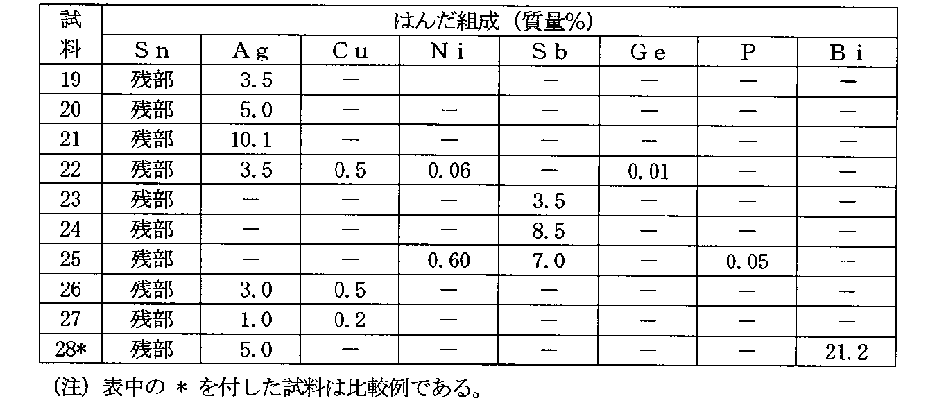
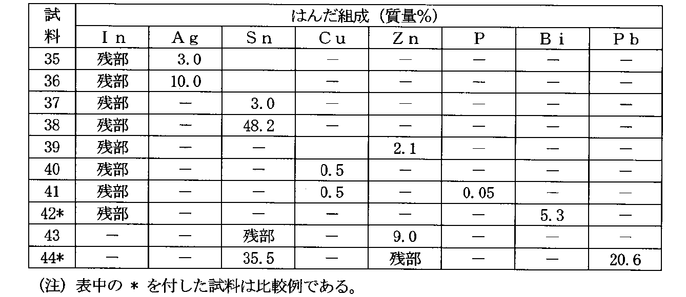
- the composition of each of the obtained solder mother alloys of Samples 1 to 44 was analyzed using an ICP emission spectroscopic analyzer (SHIMAZU S-8100). The obtained analysis results are shown in Tables 1 to 5 below as solder compositions.
- Samples 1 to 8 in Table 1 are Bi-based alloys including the first to fourth solder compositions
- Samples 9 to 18 in Table 2 are Pb-based alloys including the fifth solder composition
- Sample 19 in Table 3 28 to Sn alloy containing the sixth solder composition
- samples 29 to 34 in Table 4 are Au alloy containing the seventh solder composition
- samples 35 to 42 in Table 5 are the eighth solder composition.
- Samples 43 to 44 are Sn-based and Zn-based alloys including the ninth solder composition.
- the workability of the solder alloy was evaluated by processing each of the solder mother alloys of Samples 1 to 44 shown in Tables 1 to 5 into a sheet shape with a rolling mill as described below. That is, after each solder mother alloy (plate-like ingot having a thickness of 5 mm) was rolled while adjusting the feed speed of the ingot, and after rough rolling (warm rolling at a rolling temperature of 90 ° C.) to a thickness of 400 ⁇ m, The final finish rolling was performed at room temperature up to a thickness of 100 ⁇ m using a rolling roll having a surface roughness (Ra) of 0.1 ⁇ m.
- Ra surface roughness
- each solder alloy rolled into a sheet as described above was cut into a width of 25 mm by slitting.
- polishing was performed by buffing (abrasive grains: 0.1 ⁇ m) to obtain a predetermined surface roughness.
- the substrate was acid-washed with dilute sulfuric acid for 1 to 10 minutes, washed with water to thoroughly wash out the acid, further washed with ethanol, and then vacuum-dried at room temperature in a vacuum oven.
- surface polishing is often not performed, and even when acid cleaning is performed, dilute sulfuric acid is not always used, but in this embodiment, the oxide layer, surface roughness, and the like are adjusted. Therefore, it was intentionally manufactured under the above conditions.
- the thickness and surface roughness (Ra) of the oxide layer were measured for each of the solder alloys of the obtained sheet-like samples 1 to 44.
- the thickness of the oxide layer was measured using a field emission Auger electron spectrometer (manufactured by ULVAC-PHI, model: SAM-4300), and the surface roughness (Ra) was measured by a surface roughness measuring device (manufactured by Tokyo Seimitsu Co., Ltd.). Measurement was performed using a model: Surfcom 470A).
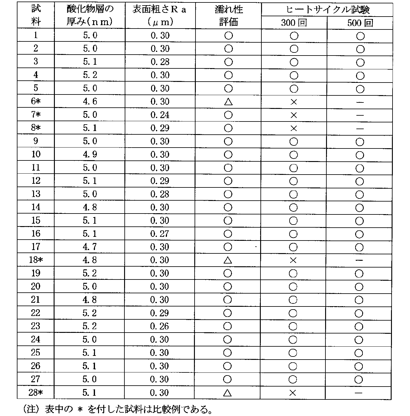
- the measurement results of the thickness and surface roughness (Ra) of the obtained oxide layer are shown in Tables 6 to 7 below.
- solder wettability was evaluated by the following method and the reliability was evaluated by a heat cycle test.
- the evaluation of solder wettability or bondability does not depend on the shape of the solder, so it may be evaluated by the shape of a wire, a ball or the like.
- the solder alloy of each sample was placed on a Cu substrate and heated for 25 seconds. After the heating was completed, the Cu substrate was taken up from the heater part, and once installed in a place where the nitrogen atmosphere next to it was kept, it was cooled. After sufficiently cooling, it was taken out into the atmosphere and a joint portion was confirmed. The joint between the solder alloy and the Cu substrate of each sample was visually confirmed, and “ ⁇ (defect)” when the joint could not be joined, and “ ⁇ ( “Yes”), the case where the bonding was possible and the wet spread was good (the state where the solder was thin and wet spread) was evaluated as “ ⁇ (good)”.
- ⁇ Heat cycle test> A heat cycle test was conducted to evaluate the reliability of solder joints. This test was performed using two samples each of which the solder alloy could be bonded to the Cu substrate in the above-described evaluation of wettability (samples having a wettability evaluation of ⁇ and ⁇ ). That is, a heat cycle test was performed on two Cu substrates to which the solder alloys of each sample were bonded, with one cycle consisting of cooling at ⁇ 55 ° C. and heating at + 150 ° C. One of these two was halfway The heat cycle test was repeated up to 300 cycles for confirmation and the remaining one up to 500 cycles.
- the composition range was an appropriate range
- the thickness of the oxide layer on the solder surface was as thin as 120 nm or less
- the surface roughness (Ra) was adjusted to 0.60 ⁇ m or less. This is considered to be because the presence of oxygen that hinders the bonding between the electronic component and the substrate is suppressed as much as possible. Further, the high reliability is also considered to be due to the connection under the condition of suppressing the presence of oxygen as much as possible together with the adjustment control of the thickness and surface roughness (Ra) of the oxide layer.
- Samples 6 to 8 (Bi system), Sample 18 (Pb system), Sample 28 (Sn system), Sample 34 (Au system), Sample 42 (In system) and Sample 44 (Zn system) are comparative examples.
- Each solder alloy has undesirable results due to the inadequate solder composition range. That is, with regard to the wettability, good results were not obtained for Sample 6, Sample 18, Sample 28, Sample 42, and Sample 44. Furthermore, in the heat cycle test, defects occurred by 300 cycles in all the samples of the comparative examples.
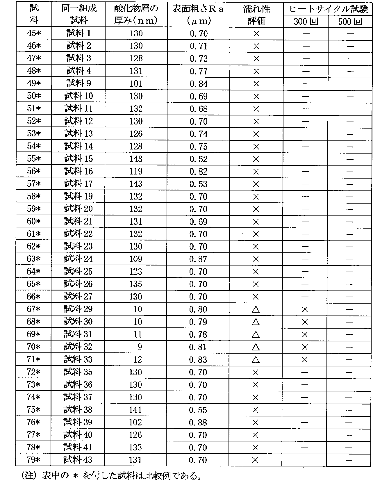
- Example 1 Each solder composition of the present invention in Example 1 above, that is, samples 1 to 4 in Table 1, samples 9 to 17 in Table 2, samples 19 to 27 in Table 3, samples 29 to 33 in Table 4, and tables
- the raw materials were prepared so as to have the same composition as each of the solder compositions of Samples 35 to 41 and Sample 43 of No. 5, and processed into a sheet shape under the following conditions to produce each solder alloy of the comparative example.
- composition analysis results of samples 45 to 79 are the same as the solder compositions of the samples shown in Tables 1 to 5 of Example 1 described above.
- the corresponding sample numbers in Tables 1 to 5 are shown in the table below for reference. 8 is displayed.
Landscapes
- Chemical & Material Sciences (AREA)
- Engineering & Computer Science (AREA)
- Mechanical Engineering (AREA)
- Materials Engineering (AREA)
- Metallurgy (AREA)
- Organic Chemistry (AREA)
- Microelectronics & Electronic Packaging (AREA)
- Electric Connection Of Electric Components To Printed Circuits (AREA)
Description
第2のはんだ合金はZnを0.01質量%以上13.5質量%以下含有する上記第1のはんだ合金である。
第3のはんだ合金はAgを0.01質量%以上12.0質量%以下含有する上記第1のはんだ合金である。
第5のはんだ合金は、Pbを主成分とし、第2元素群としてSn、Ag、Cu、In、Te及びPのうち少なくとも1種を含有し、Pbと第2元素群の合計が80質量%以上である。
第6のはんだ合金は、Snを主成分とし、第2元素群としてAg、Sb、Cu、Ni、Ge及びPのうち少なくとも1種を含有し、Snと第2元素群の合計が80質量%以上である。
第7のはんだ合金は、Auを主成分とし、第2元素群としてGe、Sn及びSiのうち少なくとも1種を含有し、Auと第2元素群の合計が90質量%以上である。
第8のはんだ合金は、Inを40質量%以上含有し、Ag、Sn、Cu、Zn及びPのうち少なくとも1種を含有する。
第9のはんだ合金は、ZnとSnを合計80質量%以上含有し、Alを含んでいない。
本発明においては、はんだ合金の酸化物層の厚みを120nm以下に制御することが必須の条件である。酸化物層の厚みを120nm以下にすることによって、濡れ性及び接合性を向上させることができ、引いては高い接合信頼性を得ることができるからである。
本発明においては、上記したように酸化物層の厚みを120nm以下に制御することと共に、はんだの表面粗さ(Ra)を0.60μm以下に調整することが、濡れ性及び接合性を向上させ、引いては高い接合信頼性を得るための必須の条件である。
本発明において、はんだ合金の製造方法自体は特に限定されない。即ち、原料の溶解方法は、抵抗加熱法、還元拡散法、高周波溶解法などで行ってよく、特に高周波溶解法は高融点の金属でも短時間で効率よく溶解できるため好ましい。但し、溶解時や鋳込み時に酸素が存在すると合金の酸化が進むだけではなく、鋳込み時に酸化膜を巻き込むため酸化膜が厚くなったり、表面粗さが大きくなったりしてしまう。これらを防ぐため、溶解時は不活性ガスを流し、更に鋳型の溶湯入口にも不活性ガスを流すことが好ましい。微粉を製造する場合は気中または液中アトマイズ法を用いてよく、ディスク式アトマイズ法などを用いてもよい。
本発明のはんだ合金は、上記したように酸化物層の厚みを120nm以下とし且つ表面粗さ(Ra)を0.60μm以下とすることが必須の条件であるが、同時に、適切なはんだ組成を選定することが必要である。即ち、本発明によるはんだ合金は、その組成について満たすべき範囲があり、具体的には以下に列挙する9種類の組成を有することが必要である。
原料として、それぞれ純度99.9質量%以上のBi、Zn、Ag、Sn、Pb、Cu、Au、In、Al、Ni、Sb、Ge、Te、Si及びPを準備した。大きな薄片やバルク状の原料については、溶解後の合金においてサンプリング場所による組成のバラツキがなく、均一になるように留意しながら、切断及び粉砕などにより3mm以下の大きさに細かくした。次に、これら原料から所定量を秤量して、高周波溶解炉用のグラファイト製坩堝に入れた。



上記のごとくシート状に加工した各はんだ合金を、濡れ性試験機(装置名:雰囲気制御式濡れ性試験機)を用いて評価した。即ち、濡れ性試験機のヒーター部に2重のカバーをして、ヒーター部の周囲4箇所から窒素を12リットル/分の流量で流しながら、ヒーター設定温度を融点より50℃高い温度にして加熱した。設定したヒーター温度が安定した後、Cu基板(板厚:約0.70mm)をヒーター部にセッティングして25秒間加熱した。
はんだ接合の信頼性を評価するためにヒートサイクル試験を行った。この試験は、上記した濡れ性の評価においてはんだ合金がCu基板に接合できた試料(濡れ性の評価が○及び△の試料)を各2個ずつ用いて行った。即ち、各試料のはんだ合金が接合されたCu基板2個に対して、-55℃の冷却と+150℃の加熱を1サイクルとするヒートサイクル試験を実施し、これら2個のうち1個は途中確認のため300サイクルまで、残りの1個は500サイクルまでヒートサイクル試験を繰り返した。

上記実施例1における本発明の各はんだ組成、即ち、上記した表1の試料1~4、表2の試料9~17、表3の試料19~27、表4の試料29~33、及び表5の試料35~41及び試料43の各はんだ組成と同じの組成になるように原料を調合し、以下の条件によりシート状に加工して比較例の各はんだ合金を作製した。
Claims (10)
- Biを85質量%以上含有し、酸化物層の厚みが120nm以下であって、表面粗さ(Ra)が0.60μm以下であるはんだ合金。
- Znを0.01質量%以上13.5質量%以下含有する、請求項1に記載のはんだ合金。
- Agを0.01質量%以上12.0質量%以下含有する、請求項1に記載のはんだ合金。
- Biを40質量%以上85質量%未満含有し、Snを60質量%以下含有し、BiとSn以外の元素を含有する場合その含有量は5質量%以下であり、酸化物層の厚みが120nm以下であって、表面粗さ(Ra)が0.60μm以下であるはんだ合金。
- Pbを主成分とし、第2元素群としてSn、Ag、Cu、In、Te及びPのうち少なくとも1種を含有し、Pbと第2元素群の合計が80質量%以上であり、酸化物層の厚みが120nm以下であって、表面粗さ(Ra)が0.60μm以下であるはんだ合金。
- Snを主成分とし、第2元素群としてAg、Sb、Cu、Ni、Ge及びPのうち少なくとも1種を含有し、Snと第2元素群の合計が80質量%以上であり、酸化物層の厚みが120nm以下であって、表面粗さ(Ra)が0.60μm以下であるはんだ合金。
- Auを主成分とし、第2元素群としてGe、Sn及びSiのうち少なくとも1種を含有し、Auと第2元素群の合計が90質量%以上であり、酸化物層が120nm以下であって、表面粗さ(Ra)が0.60μm以下であるはんだ合金。
- Inを40質量%以上含有し、Ag、Sn、Cu、Zn及びPのうち少なくとも1種を含有し、酸化物層の厚みが120nm以下であって、表面粗さ(Ra)が0.60μm以下であるはんだ合金。
- ZnとSnを合計80質量%以上含有し、Alを含まず、酸化物層の厚みが120nm以下であって、表面粗さ(Ra)が0.60μm以下であるはんだ合金。
- 請求項1~9に記載のはんだ合金によって接合された電子部品を有している電子装置。
Priority Applications (4)
| Application Number | Priority Date | Filing Date | Title |
|---|---|---|---|
| GB1502723.8A GB2519276A (en) | 2012-07-26 | 2013-07-24 | Solder alloy |
| CN201380039591.7A CN104640668A (zh) | 2012-07-26 | 2013-07-24 | 焊料合金 |
| DE201311003654 DE112013003654T5 (de) | 2012-07-26 | 2013-07-24 | Lötlegierung |
| US14/416,130 US20150196978A1 (en) | 2012-07-26 | 2013-07-24 | Solder alloy |
Applications Claiming Priority (2)
| Application Number | Priority Date | Filing Date | Title |
|---|---|---|---|
| JP2012165344A JP2014024082A (ja) | 2012-07-26 | 2012-07-26 | はんだ合金 |
| JP2012-165344 | 2012-07-26 |
Publications (1)
| Publication Number | Publication Date |
|---|---|
| WO2014017568A1 true WO2014017568A1 (ja) | 2014-01-30 |
Family
ID=49997377
Family Applications (1)
| Application Number | Title | Priority Date | Filing Date |
|---|---|---|---|
| PCT/JP2013/070122 Ceased WO2014017568A1 (ja) | 2012-07-26 | 2013-07-24 | はんだ合金 |
Country Status (7)
| Country | Link |
|---|---|
| US (1) | US20150196978A1 (ja) |
| JP (1) | JP2014024082A (ja) |
| CN (1) | CN104640668A (ja) |
| DE (1) | DE112013003654T5 (ja) |
| GB (1) | GB2519276A (ja) |
| TW (1) | TW201418477A (ja) |
| WO (1) | WO2014017568A1 (ja) |
Cited By (3)
| Publication number | Priority date | Publication date | Assignee | Title |
|---|---|---|---|---|
| JP2017110195A (ja) * | 2015-12-16 | 2017-06-22 | 三洋化成工業株式会社 | 活性エネルギー線硬化型耐指紋性付与剤 |
| US10493567B2 (en) | 2017-05-11 | 2019-12-03 | Panasonic Intellectual Property Management Co., Ltd. | Solder alloy and bonded structure using the same |
| WO2023026754A1 (ja) * | 2021-08-27 | 2023-03-02 | デクセリアルズ株式会社 | はんだ粒子、はんだ粒子の製造方法、及び導電性組成物 |
Families Citing this family (17)
| Publication number | Priority date | Publication date | Assignee | Title |
|---|---|---|---|---|
| US10633754B2 (en) * | 2013-07-05 | 2020-04-28 | The Boeing Company | Methods and apparatuses for mitigating tin whisker growth on tin and tin-plated surfaces by doping tin with germanium |
| US10811376B2 (en) * | 2014-09-09 | 2020-10-20 | Senju Metal Industry Co., Ltd. | Cu column, Cu core column, solder joint, and through-silicon via |
| JP2016087608A (ja) * | 2014-10-29 | 2016-05-23 | 住友金属鉱山株式会社 | エネルギー吸収量が制御されたPbフリーAu−Ge−Sn系はんだ合金及びこれを用いて封止若しくは接合された電子部品 |
| CN105014254B (zh) * | 2015-07-30 | 2017-07-11 | 苏州宇邦新型材料股份有限公司 | 一种光伏焊带用耐腐蚀低温焊料及其制备方法 |
| JP6677869B2 (ja) * | 2015-11-30 | 2020-04-08 | 三菱マテリアル株式会社 | はんだ粉末の製造方法 |
| CN106695163A (zh) * | 2016-12-29 | 2017-05-24 | 安徽华众焊业有限公司 | 一种金基软焊料及其制备方法 |
| CN107297582B (zh) * | 2016-12-29 | 2019-08-27 | 北京有色金属与稀土应用研究所 | 一种免清洗铅基高温焊膏及其制备方法 |
| MX2019010553A (es) * | 2017-04-10 | 2019-11-21 | Metallo Belgium | Proceso mejorado para la produccion de soldadura cruda. |
| CN106914711B (zh) * | 2017-04-13 | 2019-04-23 | 杭州哈尔斯实业有限公司 | 一种不锈钢真空容器用无铅焊料及其制造方法和钎焊方法 |
| JPWO2020044650A1 (ja) * | 2018-08-31 | 2021-08-10 | Jx金属株式会社 | はんだ合金 |
| DE102019103140A1 (de) * | 2019-02-08 | 2020-08-13 | Jenoptik Optical Systems Gmbh | Verfahren zum Löten eines oder mehrerer Bauteile |
| EP3718678A1 (de) * | 2019-04-03 | 2020-10-07 | Felder GmbH Löttechnik | Verfahren zur herstellung eines snbi-lötdrahtes, lötdraht und vorrichtung |
| US11819955B2 (en) | 2019-05-27 | 2023-11-21 | Senju Metal Industry Co., Ltd. | Solder alloy, solder paste, solder ball, solder preform, solder joint, on-board electronic circuit, ECU electronic circuit, on-board electronic circuit device, and ECU electronic circuit device |
| JP6649596B1 (ja) * | 2019-05-27 | 2020-02-19 | 千住金属工業株式会社 | はんだ合金、はんだ粉末、およびはんだ継手 |
| WO2020241544A1 (ja) * | 2019-05-27 | 2020-12-03 | 千住金属工業株式会社 | はんだペースト及びはんだペースト用フラックス |
| JP6810372B1 (ja) * | 2019-05-27 | 2021-01-06 | 千住金属工業株式会社 | はんだ合金、ソルダペースト、はんだボール、ソルダプリフォーム、はんだ継手、および回路 |
| CN117940248A (zh) * | 2022-08-24 | 2024-04-26 | 株式会社田村制作所 | 软钎料合金、接合部、接合材料、焊膏、接合结构体和电子控制装置 |
Citations (6)
| Publication number | Priority date | Publication date | Assignee | Title |
|---|---|---|---|---|
| JPH07284983A (ja) * | 1994-04-20 | 1995-10-31 | Tanaka Denshi Kogyo Kk | 半田材料及びその製造方法 |
| JP2001150182A (ja) * | 1999-11-22 | 2001-06-05 | Mitsubishi Materials Corp | 濡れ性に優れた金錫合金ロウ材 |
| JP2004209494A (ja) * | 2002-12-27 | 2004-07-29 | Mitsui Mining & Smelting Co Ltd | はんだペースト用はんだ粉 |
| JP2009125753A (ja) * | 2007-11-20 | 2009-06-11 | Toyota Central R&D Labs Inc | はんだ材料及びその製造方法、接合体及びその製造方法、並びにパワー半導体モジュール及びその製造方法 |
| JP2010036234A (ja) * | 2008-08-07 | 2010-02-18 | Mitsui Mining & Smelting Co Ltd | はんだ粉及びはんだペースト |
| JP2012228729A (ja) * | 2011-04-27 | 2012-11-22 | Sumitomo Metal Mining Co Ltd | Znを主成分とするPbフリーはんだ合金およびその製造方法 |
-
2012
- 2012-07-26 JP JP2012165344A patent/JP2014024082A/ja active Pending
-
2013
- 2013-07-24 DE DE201311003654 patent/DE112013003654T5/de not_active Withdrawn
- 2013-07-24 WO PCT/JP2013/070122 patent/WO2014017568A1/ja not_active Ceased
- 2013-07-24 GB GB1502723.8A patent/GB2519276A/en not_active Withdrawn
- 2013-07-24 US US14/416,130 patent/US20150196978A1/en not_active Abandoned
- 2013-07-24 CN CN201380039591.7A patent/CN104640668A/zh active Pending
- 2013-07-26 TW TW102126860A patent/TW201418477A/zh unknown
Patent Citations (6)
| Publication number | Priority date | Publication date | Assignee | Title |
|---|---|---|---|---|
| JPH07284983A (ja) * | 1994-04-20 | 1995-10-31 | Tanaka Denshi Kogyo Kk | 半田材料及びその製造方法 |
| JP2001150182A (ja) * | 1999-11-22 | 2001-06-05 | Mitsubishi Materials Corp | 濡れ性に優れた金錫合金ロウ材 |
| JP2004209494A (ja) * | 2002-12-27 | 2004-07-29 | Mitsui Mining & Smelting Co Ltd | はんだペースト用はんだ粉 |
| JP2009125753A (ja) * | 2007-11-20 | 2009-06-11 | Toyota Central R&D Labs Inc | はんだ材料及びその製造方法、接合体及びその製造方法、並びにパワー半導体モジュール及びその製造方法 |
| JP2010036234A (ja) * | 2008-08-07 | 2010-02-18 | Mitsui Mining & Smelting Co Ltd | はんだ粉及びはんだペースト |
| JP2012228729A (ja) * | 2011-04-27 | 2012-11-22 | Sumitomo Metal Mining Co Ltd | Znを主成分とするPbフリーはんだ合金およびその製造方法 |
Cited By (5)
| Publication number | Priority date | Publication date | Assignee | Title |
|---|---|---|---|---|
| JP2017110195A (ja) * | 2015-12-16 | 2017-06-22 | 三洋化成工業株式会社 | 活性エネルギー線硬化型耐指紋性付与剤 |
| US10493567B2 (en) | 2017-05-11 | 2019-12-03 | Panasonic Intellectual Property Management Co., Ltd. | Solder alloy and bonded structure using the same |
| WO2023026754A1 (ja) * | 2021-08-27 | 2023-03-02 | デクセリアルズ株式会社 | はんだ粒子、はんだ粒子の製造方法、及び導電性組成物 |
| JP2023032620A (ja) * | 2021-08-27 | 2023-03-09 | デクセリアルズ株式会社 | はんだ粒子、はんだ粒子の製造方法、及び導電性組成物 |
| JP7775559B2 (ja) | 2021-08-27 | 2025-11-26 | デクセリアルズ株式会社 | はんだ粒子、はんだ粒子の製造方法、及び導電性組成物 |
Also Published As
| Publication number | Publication date |
|---|---|
| JP2014024082A (ja) | 2014-02-06 |
| US20150196978A1 (en) | 2015-07-16 |
| TW201418477A (zh) | 2014-05-16 |
| GB2519276A (en) | 2015-04-15 |
| GB201502723D0 (en) | 2015-04-01 |
| CN104640668A (zh) | 2015-05-20 |
| DE112013003654T5 (de) | 2015-04-23 |
Similar Documents
| Publication | Publication Date | Title |
|---|---|---|
| WO2014017568A1 (ja) | はんだ合金 | |
| TWI440519B (zh) | 以Zn為主成分之無Pb焊料合金 | |
| JP2018079480A (ja) | 低温用のBi−In−Sn系はんだ合金、それを用いた電子部品実装基板及びその実装基板を搭載した装置 | |
| WO2012002147A1 (ja) | Pbフリーはんだ合金 | |
| JP5672132B2 (ja) | Znを主成分とするPbフリーはんだ合金およびその製造方法 | |
| JP5962461B2 (ja) | Au−Ge−Sn系はんだ合金 | |
| JP5716332B2 (ja) | Pbフリーはんだ合金 | |
| JP5093260B2 (ja) | Pbフリーはんだ合金 | |
| JP2014093425A (ja) | Znを主成分とするはんだ合金との接合部を有する電子部品 | |
| JP2013052433A (ja) | PbフリーZn系はんだ合金 | |
| JP2013123741A (ja) | 塑性変形性に優れたPbフリーはんだ合金 | |
| JP5652001B2 (ja) | Znを主成分とするPbフリーはんだ合金 | |
| JP6011254B2 (ja) | Biを主成分とするはんだ合金との接合部を有する電子部品 | |
| JP2017035708A (ja) | Pbを含まないSb−Cu系はんだ合金 | |
| JP5471985B2 (ja) | Znを主成分とするPbフリーはんだ合金 | |
| JP2016016453A (ja) | Au−Ge−Sn系はんだ合金 | |
| JP2017225979A (ja) | 高温用PbフリーZn系はんだ合金 | |
| JP5699898B2 (ja) | Znを主成分とするPbフリーはんだ合金 | |
| JP5861526B2 (ja) | Pbを含まないGe−Al系はんだ合金 | |
| JP6128062B2 (ja) | Au−Ge−Sn系はんだ合金 | |
| JP2011235314A (ja) | Znを主成分とするPbフリーはんだ合金 | |
| JP2018065170A (ja) | 高温用PbフリーZn−Al−Ag系はんだ合金及びそれを用いた電子部品 | |
| JP2011240372A (ja) | Znを主成分とするPbフリーはんだ合金 | |
| JP2016165753A (ja) | Pbを主成分とするはんだ合金 | |
| JP2011235315A (ja) | Znを主成分とするPbフリーはんだ合金 |
Legal Events
| Date | Code | Title | Description |
|---|---|---|---|
| 121 | Ep: the epo has been informed by wipo that ep was designated in this application |
Ref document number: 13822433 Country of ref document: EP Kind code of ref document: A1 |
|
| WWE | Wipo information: entry into national phase |
Ref document number: 14416130 Country of ref document: US |
|
| WWE | Wipo information: entry into national phase |
Ref document number: 112013003654 Country of ref document: DE Ref document number: 1120130036541 Country of ref document: DE |
|
| ENP | Entry into the national phase |
Ref document number: 1502723 Country of ref document: GB Kind code of ref document: A Free format text: PCT FILING DATE = 20130724 |
|
| WWE | Wipo information: entry into national phase |
Ref document number: 1502723.8 Country of ref document: GB |
|
| 122 | Ep: pct application non-entry in european phase |
Ref document number: 13822433 Country of ref document: EP Kind code of ref document: A1 |