WO2014013733A1 - 支持装置、移動体装置、露光装置、及びデバイス製造方法 - Google Patents
支持装置、移動体装置、露光装置、及びデバイス製造方法 Download PDFInfo
- Publication number
- WO2014013733A1 WO2014013733A1 PCT/JP2013/004370 JP2013004370W WO2014013733A1 WO 2014013733 A1 WO2014013733 A1 WO 2014013733A1 JP 2013004370 W JP2013004370 W JP 2013004370W WO 2014013733 A1 WO2014013733 A1 WO 2014013733A1
- Authority
- WO
- WIPO (PCT)
- Prior art keywords
- support
- support device
- force
- moving
- surface plate
- Prior art date
- Legal status (The legal status is an assumption and is not a legal conclusion. Google has not performed a legal analysis and makes no representation as to the accuracy of the status listed.)
- Ceased
Links
Images


Classifications
-
- G—PHYSICS
- G03—PHOTOGRAPHY; CINEMATOGRAPHY; ANALOGOUS TECHNIQUES USING WAVES OTHER THAN OPTICAL WAVES; ELECTROGRAPHY; HOLOGRAPHY
- G03F—PHOTOMECHANICAL PRODUCTION OF TEXTURED OR PATTERNED SURFACES, e.g. FOR PRINTING, FOR PROCESSING OF SEMICONDUCTOR DEVICES; MATERIALS THEREFOR; ORIGINALS THEREFOR; APPARATUS SPECIALLY ADAPTED THEREFOR
- G03F7/00—Photomechanical, e.g. photolithographic, production of textured or patterned surfaces, e.g. printing surfaces; Materials therefor, e.g. comprising photoresists; Apparatus specially adapted therefor
- G03F7/70—Microphotolithographic exposure; Apparatus therefor
- G03F7/70691—Handling of masks or workpieces
- G03F7/70758—Drive means, e.g. actuators, motors for long- or short-stroke modules or fine or coarse driving
Definitions
- the present invention relates to a support apparatus, a moving body apparatus, an exposure apparatus, and a device manufacturing method. More specifically, the present invention relates to a support apparatus that supports a predetermined support object from below, and moves on a base member supported by the support apparatus. The present invention relates to a moving body apparatus including a moving body, an exposure apparatus including the moving body apparatus, and a device manufacturing method using the exposure apparatus.
- steppers step-and-repeat projection exposure apparatuses
- step-and- A scanning projection exposure apparatus a so-called scanning stepper (also called a scanner) or the like is used.
- a substrate stage that holds a substrate such as a wafer or a glass plate (hereinafter collectively referred to as a wafer), which is an object to be exposed, has a movable element of the substrate stage and a predetermined base member.
- a substrate stage device that is driven two-dimensionally using a planar motor including a stator is known (see, for example, Patent Document 1).
- a moment (so-called pitching) about an axis perpendicular to the traveling direction of the substrate stage is caused by the driving force (thrust).
- Moment acts on the base member, and the vibration caused by the moment may deteriorate the exposure accuracy.
- the present invention is a support device that supports a support object in a predetermined direction with respect to a predetermined support portion, and the support object includes At least a part of the first member is provided on the first member, the first member having a facing member and a casing to which a fluid for generating a first force for supporting is supplied.
- an actuator that applies a second force in a direction along the predetermined direction and a counter member that is supported so as to be relatively movable along the predetermined direction, and the actuator applies the second force to the counter member.
- a moving member that moves in a direction opposite to the direction of the second force when acting on the opposing member.
- the moving member moves relative to the opposing member in a direction opposite to the direction of the second force, so that the reaction force against the predetermined support portion Propagation of vibration (or vibration caused by reaction force) is suppressed.
- a movable body device including a base member, a movable body movable on the base member, and the support device of the present invention using the base member as the support object. is there.
- the position control of the movable body can be performed with high accuracy.
- a moving body apparatus in which a predetermined object is held by the moving body, and a pattern forming apparatus that forms a predetermined pattern on the object using an energy beam.
- An exposure apparatus provided.
- the present invention is a device manufacturing method including exposing the object using the exposure apparatus of the present invention and developing the exposed object.
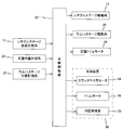
- FIG. 3 is a block diagram showing an input / output relationship of a main controller that mainly constitutes a control system of an exposure apparatus. It is sectional drawing of the support apparatus which concerns on a modification.
- FIG. 1 schematically shows a configuration of an exposure apparatus 10 according to an embodiment.
- the exposure apparatus 10 is a step-and-scan projection exposure apparatus, a so-called scanner.
- a projection optical system 16b is provided.
- the direction parallel to the optical axis AX of the projection optical system 16b is the Z-axis direction
- the reticle is in a plane perpendicular to the Z-axis direction.
- the direction in which the wafer is relatively scanned is the Y-axis direction
- the direction orthogonal to the Z-axis and the Y-axis is the X-axis direction
- the rotation (tilt) directions around the X-axis, Y-axis, and Z-axis are ⁇ x, ⁇ y, And the ⁇ z direction will be described.
- the exposure apparatus 10 includes an illumination system 12, a reticle stage 14, a projection unit 16, a wafer stage apparatus 20, and a control system thereof.
- the illumination system 12 includes, for example, a light source, an illuminance uniformizing optical system including an optical integrator, a reticle blind, and the like (both not shown) as disclosed in, for example, US Patent Application Publication No. 2003/0025890. And an illumination optical system.
- the illumination system 12 illuminates a slit-shaped illumination area IAR on the reticle R set (restricted) by a reticle blind (also called a masking system) with illumination light (exposure light) IL with substantially uniform illuminance.
- a reticle blind also called a masking system
- illumination light IL Exposure light
- ArF excimer laser light Wavelength 193 nm
- the reticle stage 14 holds a reticle R having a circuit pattern or the like formed on a pattern surface (the surface on the ⁇ Z side in FIG. 1) by, for example, vacuum suction.
- the reticle stage 14 can be driven with a predetermined stroke in the scanning direction (Y-axis direction) by a reticle stage drive system 13 (not shown in FIG. 1, see FIG. 3) including a linear motor, for example, and the X-axis and ⁇ z. It can be driven minutely in the direction.
- Position information (including rotation amount information in the ⁇ z direction) of the reticle stage 14 in the XY plane is, for example, a reticle stage position measurement system 15 (not shown in FIG. 1) including a laser interferometer system (or two-dimensional encoder system). 3) is obtained by the main controller 50 (see FIG. 3).
- the projection unit 16 is disposed below the reticle stage 14 ( ⁇ Z side).
- the projection unit 16 includes a lens barrel 16a and a projection optical system 16b held in the lens barrel 16a.
- a projection optical system 16b for example, a refractive optical system including a plurality of optical elements (lens elements) arranged along the optical axis AX is used.
- the projection optical system 16b is, for example, both-side telecentric and has a predetermined projection magnification (for example, 1/4 times, 1/5 times, or 1/8 times).
- the reticle in which the first surface (object surface) of the projection optical system 16b and the pattern surface are substantially coincided with each other is arranged. Due to the illumination light IL that has passed through R, a reduced image of the circuit pattern of the reticle R in the illumination area IAR (a reduced image of a part of the circuit pattern) passes through the projection optical system 16b, and the second surface of the projection optical system 16b.
- an exposure area IA that is conjugated to the illumination area IAR on the wafer W, which is disposed on the (image plane) side and on which a resist (sensitive agent) is applied.
- the reticle R moves relative to the illumination area IAR (illumination light IL) in the scanning direction, and the wafer W moves relative to the exposure area IA (illumination light IL).
- scanning exposure of one shot area (partition area) on the wafer W is performed, and the pattern of the reticle R is transferred to the shot area.
- the pattern of the reticle R is generated on the wafer W by the illumination system 12 and the projection optical system 16b, and the sensitive layer (resist layer) on the wafer W is exposed on the wafer W by the illumination light IL. That pattern is formed.
- the wafer stage apparatus 20 includes a surface plate 22, a wafer stage 24, a wafer stage drive system 26 (not shown in FIG. 1, refer to FIG. 3), a surface plate trim motor 28, and the like.
- the surface plate 22 is a rectangular plate-like member having the Y-axis direction as the longitudinal direction in plan view (viewed from the + Z direction), and a plurality of support devices such that the upper surface is substantially parallel to the XY plane (horizontal plane). 30 is supported non-contact from below.
- four support devices 30 are provided so that the vicinity of the four corners of the surface plate 22 can be supported.
- FIG. 1 for example, two of the four support devices 30 on the + X side are provided. Only the other two are hidden behind the two support devices 30 on the + X side. The configuration and function of the support device 30 will be described later.
- the surface plate 22 can be configured to be provided with a weight (not shown) so as to increase its own weight in order to function as a counter mass of the wafer stage 24.
- the surface plate 22 is provided with a plurality of coil units 26a in a matrix in a plan view in the region on the upper surface side inside the platen 22.
- the magnitude and direction of the current supplied to each of the plurality of coil units 26a is controlled by the main controller 50 (not shown in FIG. 1, see FIG. 3).
- the wafer stage 24 is made of a box-shaped (cuboid) member, and holds the wafer W placed on the upper surface by, for example, vacuum suction.
- a plurality of magnet units 26 b are arranged in a region on the bottom surface (surface facing the top surface of the surface plate 22) of the wafer stage 24.
- the wafer stage drive system 26 (not shown in FIG. 1, refer to FIG. 3) includes a moving magnet type planar motor including a plurality of magnet units 26b and a plurality of coil units 26a.
- the wafer stage 24 is driven with respect to the surface plate 22 by electromagnetic force (Lorentz force) acting between the plurality of magnet units 26b and the coil unit 26a corresponding to the magnet unit 26b.
- the wafer stage 24 is moved to the surface plate 22 with 6 degrees of freedom by the Lorentz force.
- a so-called 6 DOF (degrees of ⁇ freedom) planar motor that can be appropriately driven in the direction (X-axis direction, Y-axis direction, Z-axis direction, ⁇ x direction, ⁇ y direction, and ⁇ z direction) is used.
- main controller 50 (not shown in FIG. 1; see FIG. 3) uses wafer stage drive system 26 (not shown in FIG. 1, see FIG. 3) to move wafer stage 24 on surface plate 22 X.
- the position information of the wafer stage 24 in the direction of six degrees of freedom includes, for example, a wafer stage position measurement including a two-dimensional (or three-dimensional) encoder system or an optical interferometer system (or a system combining an encoder system and an optical interferometer system). It is calculated
- the configuration of the wafer stage position measurement system 27 is not particularly limited as long as the position information in the 6DOF direction of the wafer stage 24 can be obtained with a desired resolution.
- the wafer stage drive system 26 (planar motor) is used along the horizontal plane with respect to the wafer stage 24 on the surface plate 22.
- the driving force is applied (in the X-axis and / or Y-axis direction)
- the reaction force of the driving force is applied to the surface plate 22 in the direction opposite to the wafer stage 24 in the horizontal plane.
- the surface plate 22 is supported in a non-contact manner by the plurality of support devices 30, the surface plate 22 moves in the direction opposite to the wafer stage 24 in the horizontal plane according to the momentum conservation law. To absorb. Thereby, generation
- the surface plate trim motor 28 is used to move the surface plate 22 to a predetermined position. For example, when the surface plate 22 moves along the XY plane by the reaction force, the surface plate 22 can be returned to a predetermined position.
- a linear motor for example, a voice coil motor
- a stator 28a installed on the floor 100 via a support column 28c and a mover 28b fixed to the side surface of the surface plate 22 is used. It is used.
- FIG. 1 only one Y trim motor is shown as a representative. However, as the surface plate trim motor 28, an X trim motor for driving the surface plate 22 in the X axis direction, and the surface plate 22 as the Y axis.
- a plurality of Y trim motors for driving in the direction are provided.
- the position information (including the rotation amount information in the ⁇ z direction) of the surface plate 22 in the XY plane is, for example, a surface plate position measurement system 23 (not shown in FIG. 1, including a laser interferometer system (or a two-dimensional encoder system)). 3), and the main controller 50 appropriately uses a plurality of surface plate trim motors 28 based on the output of the surface plate position measurement system 23.
- the surface plate 22 is moved to a predetermined position.
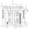
- the support device 30 includes a housing 32 including a main body 32a and a lid 32b, an air pad 36, a center shaft 38, a counter mass 40, a compression coil spring 42, and a plurality of counter mass motors 44. , And a plurality of trim motors 46.
- the main body portion 32a is formed of a bottomed cylindrical member having an upper portion (+ Z side end portion) opened, and is installed on the floor 100.
- the lid body 32b is made of a disk-like member disposed substantially parallel to the horizontal plane, and is inserted into the opening of the main body portion 32a.
- the outer diameter of the lid 32b is set smaller than the inner diameter of the main body 32a, and a gap is formed between the inner wall surface of the main body 32a and the outer peripheral end of the lid 32b.
- a gap (opening) formed between the main body portion 32a and the lid body 32b is closed by, for example, a diaphragm 34 made of a metallic film formed in a ring shape, and the lid body 32b is closed to the main body portion 32a.
- a small amount of movement is possible in the Z-axis direction.
- the housing 32 (the main body 32a, the lid 32b, and the diaphragm 34) forms a gas chamber 31 that is substantially airtight.
- the main body 32a is filled with a pressurized gas (for example, air) that is set higher than the external pressure.
- the pressure in the gas chamber 31 is set to, for example, 0.3 to 0.3 by the main controller 50 (see FIG. 3) using an internal pressure control system 33 (not shown in FIG. 1, see FIG. 3) including an electromagnetic regulator (not shown). It is controlled to about 0.4 MPa.
- the support device 30 generates a force (first force) for supporting the surface plate 22 by the action of the pressurized gas filled in the gas chamber 31 and the diaphragm 34, and the surface plate 22 and the illumination system 12, It functions as an anti-vibration device (vibration damping device) that physically (vibratingly) separates the reticle stage 14 and the projection unit 16.
- the air pad 36 is made of, for example, a disk-shaped member made of a porous member, and is fixed to the upper surface of the lid 32b. With the support device 30 supporting the surface plate 22 from below, the upper surface of the air pad 36 faces the lower surface of the surface plate 22.
- the air pad 36 is connected to a pressurized gas supply device (not shown).
- the support device 30 supports the surface plate 22 in a non-contact manner by a static pressure of a pressurized gas (for example, air) ejected from the air pad 36 toward the lower surface of the surface plate 22. Accordingly, the surface plate 22 is movable along the XY plane with respect to the plurality of support devices 30 (see FIG. 1).
- a pressurized gas for example, air
- the air pads 36 may be provided separately.
- the surface plate 22 may be supported by a configuration in which three air pads having a smaller diameter are provided on the lid 32b instead of one air pad. . It is necessary to improve the flatness of the surface of the air pad facing the surface plate 22, but using a small-diameter air pad has the advantage of facilitating processing during manufacture.
- the center shaft 38 is formed of a columnar member extending in the Z-axis direction, and a lower end portion is connected to a bottom center portion of the main body portion 32a.
- the longitudinal direction (Z-axis direction) dimension of the center shaft 38 is set to be shorter than the height direction (Z-axis direction) dimension of the main body portion 32a, and the upper end portion of the center shaft 38 is independent of the Z position of the lid 32b.
- a predetermined gap (clearance, gap) is formed between the lower surface of the lid 32b.
- the counter mass 40 is made of, for example, a cylindrical member made of a metal material or the like, and a through hole 40a penetrating in the Z-axis direction is formed at the center.
- the outer diameter of the counter mass is set to be smaller than the inner diameter of the housing 32, and a gap is formed between the inner wall surface of the main body 32 a and the outer peripheral surface of the counter mass 40.
- An air slider 41 made of a cylindrical member is integrally fixed to the inner wall surface forming the through hole 40a.
- the center shaft 38 is inserted on the inner diameter side of the air slider 41.
- a minute gap is formed between the outer peripheral surface of the center shaft 38 and the inner peripheral surface of the air slider 41.
- the air slider 41 is formed of, for example, a porous member, and is connected to a pressurized gas supply device (not shown) disposed outside the support device 30.
- the counter mass 40 is movable in the Z-axis direction along the center shaft 38 in a non-contact state by the static pressure of the pressurized gas ejected from the air slider 41 to the outer peripheral surface of the center shaft 38.
- the compression coil spring 42 is housed inside the main body 32a and supports the weight of the counter mass 40 from below.
- the outer diameter of the compression coil spring 42 is substantially the same as that of the counter mass 40, and the center shaft 38 is inserted inside the compression coil spring 42.
- the plurality of counter mass motors 44 are provided in the main body portion 32a and at least three (for example, four in this embodiment) around the center axis of the center shaft 38 at a predetermined interval.
- Each of the plurality of counter mass motors 44 includes a coil unit 44a and a magnet unit 44b.
- the coil unit 44a is fixed to the lower surface of the lid 32b via a support member 45 made of a rod-shaped member extending in the Z-axis direction and having an end on the + Z side connected to the lower surface of the lid 32b. Further, the coil unit 44 a is inserted into a recess 40 b formed on the upper surface of the counter mass 40 in a non-contact state with the counter mass 40.
- At least three recesses 40b are formed around the Z axis at predetermined intervals.
- the magnitude and direction of the current supplied to the coil units 44a of each of the plurality of counter mass motors 44 are synchronously controlled by the main controller 50 (not shown in FIG. 2, see FIG. 3).
- the magnet unit 44b is fixed to a wall surface portion forming the recess 40b and facing the coil unit 44a.
- the plurality of trim motors 46 are provided in the body portion 32a and at least three (for example, four in this embodiment) around the center axis of the center shaft 38 at a predetermined interval.
- Each of the plurality of trim motors 46 includes a coil unit 46a and a magnet unit 46b.
- the coil unit 46a is fixed to the bottom surface portion of the main body portion 32a via a support member 47 made of a rod-shaped member extending in the Z-axis direction and connected to the bottom surface portion of the main body portion 32a.
- the coil unit 46 a is inserted into a recess 40 c formed on the lower surface of the counter mass 40 in a non-contact state with the counter mass 40.
- At least three concave portions 40c are formed around the Z axis at a predetermined interval.
- the magnitude and direction of the current supplied to the coil units 46a of each of the plurality of trim motors 46 are synchronously controlled by the main controller 50 (not shown in FIG. 2, see FIG. 3).
- the magnet unit 46b is a wall surface portion that forms the recess 40c and is fixed to a portion facing the coil unit 46a.
- the plurality of counter mass motors 44 and the plurality of trim motors 46 have different radial distances from the center of the center shaft 38. Specifically, the plurality of trim motors 46 are disposed closer to the center shaft 38 than the plurality of counter mass motors 44. Thereby, the thickness of the counter mass 40 is suppressed and the support apparatus 30 is comprised compactly.
- each of the plurality of support devices 30 has substantially the same configuration and function except for the arrangement, but is independently controlled by the main control device 50.
- the plurality of counter mass motors 44 included in each of the plurality of support devices 30 are controlled independently of each other by the main controller 50 and generate a force in the Z-axis direction (second force).
- the plurality of trim motors 46 included in each of the plurality of support devices 30 are controlled independently from each other by the main control device 50.
- FIG. 3 is a block diagram showing the input / output relationship of the main controller 50 that centrally configures the control system of the exposure apparatus 10 and performs overall control of each component.
- the main controller 50 includes a workstation (or a microcomputer) and the like, and comprehensively controls each part of the exposure apparatus 10.
- the reticle R and the wafer W are loaded on the reticle stage 14 and the wafer stage 24, respectively, and reticle alignment, baseline measurement, and wafer alignment (for example, predetermined preparatory work such as EGA (Enhanced Global Alignment) is performed.
- the wafer stage 24 is driven to the acceleration start position for exposure to the first shot area of the wafer W, and the position of the reticle R is set to the acceleration start position.
- the reticle stage 14 is driven.
- the reticle stage 14 and the wafer stage 24 are synchronously driven along the Y-axis direction, whereby the first shot area on the wafer W is exposed.
- exposure of all shot areas on the reticle is performed, whereby the exposure of the wafer W is completed.
- the wafer stage 24 is appropriately driven in the direction of 6 degrees of freedom on the surface plate 22 by a wafer stage drive system 26 (see FIG. 3) including a planar motor.
- the main controller 50 controls the pressure in the gas chamber 31 of each of the plurality of support devices 30 via the internal pressure control system 33 based on the measurement value of a pressure sensor (not shown). The propagation of vibration between the floor surface 100 (see FIG. 1) and the surface plate 22 is suppressed. Further, in parallel with the pressure control in the gas chamber 31, the main controller 50 moves the surface plate 22 in the ⁇ Z direction according to the output of an acceleration sensor (not shown) that detects vibration of the surface plate 22.
- the lid 32b (and the air pad 36) is driven in the + Z direction (the direction opposite to the surface plate 22) with respect to the main body 32a by using the second force generated by the plurality of counter mass motors 44. By doing so, the vibration of the surface plate 22 is suppressed.
- the magnet unit 44b of each of the plurality of counter mass motors 44 is fixed to the counter mass 40 in the support device 30.
- a force in the ⁇ Z direction acts on the counter mass 40. Since the counter mass 40 is supported by the compression coil spring 42 in a state where the position in the Z-axis direction is not constrained, the counter mass motor is moved in the ⁇ Z direction along the center shaft 38 by the momentum conservation law.
- the drive reaction force from 44 is absorbed, whereby the drive reaction force is propagated to the floor 100 and the occurrence of vibration due to the drive reaction force is suppressed.
- the main controller 50 controls the plurality of trim motors 46 so that the vertical movement of the counter mass 40 due to the spring property of the compression coil spring 42 is suppressed. Used to control the Z position of the counter mass 40. Thereby, the posture of the counter mass 40 (that is, the magnet unit 44b of each of the plurality of counter mass motors 44) is stabilized, and the above-described vibration isolation operation can be performed with high accuracy.
- the wafer stage 24 is appropriately driven (accelerated) on the surface plate 22 in the X-axis direction and / or the Y-axis direction by a wafer stage drive system 26 (see FIG. 3) including a flat motor. Or a deceleration), a Lorentz force (electromagnetic force) in a direction parallel to the XY plane is generated between the coil unit 26a built in the surface plate 22 and the magnet unit 26b built in the wafer stage 24. .
- the coil unit 26a is disposed below the upper surface of the surface plate 22, and the magnet unit 26b is disposed above the lower surface of the wafer stage 24. Therefore, the Lorentz force is constant. It occurs between the upper surface of the board 22 and the lower surface of the wafer stage 24.
- the center of gravity of the wafer stage 24 of the present embodiment is located on the + Z side with respect to the point of action of the Lorentz force, the center of gravity of the wafer stage 24 is caused by the Lorentz force acting on the magnet unit 26b.
- a moment (so-called pitching moment) about an axis perpendicular to the advancing direction of the wafer stage 24 is applied.
- the position of the center of gravity of the surface plate 22 is located on the ⁇ Z side with respect to the point of application of the Lorentz force, the surface plate 22 also has the center of gravity centered on the wafer due to the Lorentz force acting on the coil unit 26a.
- a pitching moment in the same direction as the pitching moment acting on the stage 24 acts.
- the pitching moment causes at least one of the plurality of support devices 30 to have a downward force in the gravity direction ( Hereinafter, it is called a pitching force.
- the magnitude of the pitching force acting on the support device 30 varies depending on the position and acceleration of the wafer stage 24, but the output of the wafer stage position measurement system 27 (see FIG. 3) and the wafer stage 24 are driven (acceleration). Or based on the acceleration information when decelerating) (or after the fact in real time).
- the main control device 50 appropriately drives a plurality of counter mass motors 44 included in the support device 30 on which the pitching force acts among the plurality of support devices 30, and is approximately the same size as the pitching force (downward force in the gravity direction).
- An upward force in the gravity direction (+ Z direction) is applied to the lid 32b of the support device 30.
- the pitching force is canceled (cancelled), and the occurrence of vibration due to the direct transmission of the pitching force to the floor 100 is suppressed.
- the downward force in the gravitational direction with respect to the support device 30 is not limited to that caused by the pitching moment, and acts as a reaction force on the surface plate 22 even when the wafer stage 24 is driven in the + Z direction (or the ⁇ x and ⁇ y directions). Therefore, the same control may be performed at that time.
- the support device 30 functions as a vibration isolator that suppresses the propagation of vibration between the surface plate 22 and the floor 100, and the pitching force that acts on the floor 100 from the surface plate 22. It has a function as a counter mass device which suppresses.
- the magnet unit 44 b that is a stator of the counter mass motor 44 is fixed to the counter mass 40, the driving reaction force of the counter mass motor 44 is not transmitted directly to the floor 100. Therefore, a decrease in exposure accuracy due to the occurrence of vibration is suppressed.
- elements for exhibiting the vibration isolator function and the counter mass device function are provided in one main body 32a. Therefore, the support device 30 can be made compact and the footprint of the exposure apparatus 10 can be reduced. Furthermore, since the element is almost sealed in the main body 32a, the exposure space of the wafer is prevented from being contaminated by the element.
- the configuration of the exposure apparatus 10 of the above embodiment can be changed as appropriate.
- the main body 32a and the lid 32b of the housing 32 are connected by the diaphragm 34, but the present invention is not limited to this.
- the lid 32b can be slightly moved in the Z-axis direction with respect to the main body 32a, and the internal space formed by the main body 32a and the lid 32b can be airtight to ensure the function as a vibration isolator.
- the main body 62a and the lid 62b may be connected using the bellows 64, as in the case 62 of the support device 60 shown in FIG.
- the counter mass 40 is supported from below by the compression coil spring 42 having substantially the same diameter as the counter mass 40.
- the spring configuration ( The size, arrangement, number, etc.) can be changed as appropriate.
- a plurality of compression coil springs 72 having a smaller diameter than the compression coil spring 42 of the above-described embodiment are arranged at predetermined intervals around the Z axis (in the support device 60 shown in FIG. 3) It may be arranged. In this case, as shown in FIG.
- a recess 70d is formed on the lower surface of the counter mass 70, and a part of the compression coil spring 72 is inserted into the recess 70d in a non-contact state with the counter mass 70.
- a counter mass 40 may be supported from below by using a so-called air spring.
- the counter mass 40 is engaged with the center shaft 38 so as to be movable in the Z-axis direction in a non-contact state via the air slider 41.
- the present invention is not limited to this. is not.
- a ball spline device extendends in the Z-axis direction
- a center shaft 68 formed with a Z groove (not shown) and a pair of sleeves 71 having a plurality of balls (not shown) fixed to the counter mass 70 and inserted into the Z groove).
- the cross section of the center shaft 38 (or 68) is not limited to a circle, but may be other shapes such as a rectangle.
- the radial position around the center shaft 38 is different between the counter mass motor 44 and the trim motor 46 (the trim motor 46 is more than the counter mass motor 44.
- the present invention is not limited to this.
- the counter motor 74 and the trim motor 76 may be configured to overlap in the vertical direction (being symmetrical in the vertical direction).
- the planar motor constituting the wafer stage drive system is a 6 DOF drive type, but is not limited to this, and is a 3 DOF (X axis direction, Y axis direction, and ⁇ z direction) drive type.
- an air bearing may be attached to the lower surface of the wafer stage 24, and the wafer stage 24 may be lifted (air floating) by the static pressure of the pressurized gas ejected from the air bearing to the upper surface of the surface plate 22.
- the planar motor may be a moving coil type.
- the surface plate 22 is configured to be movable only in the X-axis and / or Y-axis directions.
- the present invention is not limited to this, and the surface plate 22 can be rotated by a small amount in the ⁇ x and ⁇ y directions. It may be configured.
- the moment of inertia of the surface plate 22 can reduce the pitching force acting on the support device 30 when the wafer stage 24 is driven, and the force generated by the plurality of counter mass motors 44 is applied to the above embodiment. Smaller than that.
- the illumination light IL is not limited to ArF excimer laser light (wavelength 193 nm), but may be ultraviolet light such as KrF excimer laser light (wavelength 248 nm) or vacuum ultraviolet light such as F 2 laser light (wavelength 157 nm). good.
- ultraviolet light such as KrF excimer laser light (wavelength 248 nm) or vacuum ultraviolet light such as F 2 laser light (wavelength 157 nm).
- vacuum ultraviolet light for example, erbium.
- a harmonic which is amplified by a fiber amplifier doped with (or both erbium and ytterbium) and wavelength-converted into ultraviolet light using a nonlinear optical crystal may be used.
- the wavelength of the illumination light IL is not limited to light of 100 nm or more, and light having a wavelength of less than 100 nm may be used.
- EUV Extreme Ultraviolet
- a soft X-ray region for example, a wavelength region of 5 to 15 nm.
- the above-described embodiment can also be applied to an EUV exposure apparatus using the above.
- the above embodiment can be applied to an exposure apparatus that uses charged particle beams such as an electron beam or an ion beam.
- the projection optical system in the exposure apparatus of the above embodiment may be not only a reduction system but also any of the same magnification and enlargement systems, and the projection optical system 16b may be any of a reflection system and a catadioptric system as well as a refraction system.
- the projected image may be an inverted image or an erect image.
- a light transmissive mask in which a predetermined light shielding pattern (or phase pattern / dimming pattern) is formed on a light transmissive substrate is used.
- a predetermined light shielding pattern or phase pattern / dimming pattern
- a light transmissive substrate is used.
- a variable shaping mask, an active mask that forms a transmission pattern, a reflection pattern, or a light emission pattern.
- a DMD Digital Micro-mirror Device
- spatial light modulator spatial light modulator
- the wafer stage apparatus 20 in which one wafer stage 24 is disposed on the surface plate 22 has been described.
- the number and type of moving bodies disposed on the surface plate 22 can be changed as appropriate.
- the embodiment described above can also be applied to a wafer stage apparatus that includes a wafer stage and a measurement stage.
- an exposure operation is performed in a state where a liquid (for example, pure water) is filled between the projection optical system and an object to be exposed (for example, a wafer).
- a liquid for example, pure water
- an object to be exposed for example, a wafer.
- the above embodiment can also be applied to a so-called immersion exposure apparatus.
- an exposure apparatus (lithography system) that forms a line-and-space pattern on a wafer W by forming interference fringes on the wafer W.
- the above embodiment can also be applied.
- the above-described embodiment can also be applied to a step-and-stitch reduction projection exposure apparatus that synthesizes a shot area and a shot area.
- two reticle patterns are synthesized on a wafer via a projection optical system, and 1 on the wafer by one scan exposure.
- the above embodiment can also be applied to an exposure apparatus that performs double exposure of two shot areas almost simultaneously.
- the object on which the pattern is to be formed in the above embodiment is not limited to the wafer, but may be another object such as a glass plate, a ceramic substrate, a film member, or a mask blank. good.
- the application of the exposure apparatus is not limited to the exposure apparatus for semiconductor manufacturing, for example, an exposure apparatus for liquid crystal that transfers a liquid crystal display element pattern to a square glass plate, an organic EL, a thin film magnetic head,
- the present invention can be widely applied to an exposure apparatus for manufacturing an image sensor (CCD or the like), a micromachine, a DNA chip, and the like.
- an image sensor CCD or the like
- a micromachine a DNA chip
- the like in order to manufacture reticles or masks used in not only microdevices such as semiconductor elements but also light exposure apparatuses, EUV exposure apparatuses, X-ray exposure apparatuses, electron beam exposure apparatuses, etc., glass substrates or silicon wafers, etc.
- the above embodiment can also be applied to an exposure apparatus that transfers a circuit pattern.
- An electronic device such as a semiconductor element includes a step of designing a function / performance of a device, a step of manufacturing a reticle based on the design step, a step of manufacturing a wafer from a silicon material, and an exposure apparatus (pattern formation) according to the above-described embodiment.
- Apparatus and a lithography step for transferring a mask (reticle) pattern onto the wafer by the exposure method, a development step for developing the exposed wafer, and an etching step for removing the exposed member other than the portion where the resist remains by etching It is manufactured through a resist removal step for removing a resist that has become unnecessary after etching, a device assembly step (including a dicing process, a bonding process, and a packaging process), an inspection step, and the like.
- the exposure method described above is executed using the exposure apparatus of the above embodiment, and a device pattern is formed on the wafer. Therefore, a highly integrated device can be manufactured with high productivity.
- the support device of the present invention is suitable for supporting a predetermined member.
- the moving body device of the present invention is suitable for moving the moving body on the base member.
- the exposure apparatus of the present invention is suitable for forming a predetermined pattern on an object.
- the device manufacturing method of the present invention is suitable for the production of micro devices.
Landscapes
- Physics & Mathematics (AREA)
- General Physics & Mathematics (AREA)
- Container, Conveyance, Adherence, Positioning, Of Wafer (AREA)
- Exposure And Positioning Against Photoresist Photosensitive Materials (AREA)
- Exposure Of Semiconductors, Excluding Electron Or Ion Beam Exposure (AREA)
Priority Applications (1)
| Application Number | Priority Date | Filing Date | Title |
|---|---|---|---|
| JP2014525723A JP6268542B2 (ja) | 2012-07-18 | 2013-07-17 | 支持装置、移動体装置、露光装置、及びデバイス製造方法 |
Applications Claiming Priority (2)
| Application Number | Priority Date | Filing Date | Title |
|---|---|---|---|
| JP2012159153 | 2012-07-18 | ||
| JP2012-159153 | 2012-07-18 |
Publications (1)
| Publication Number | Publication Date |
|---|---|
| WO2014013733A1 true WO2014013733A1 (ja) | 2014-01-23 |
Family
ID=49948572
Family Applications (1)
| Application Number | Title | Priority Date | Filing Date |
|---|---|---|---|
| PCT/JP2013/004370 Ceased WO2014013733A1 (ja) | 2012-07-18 | 2013-07-17 | 支持装置、移動体装置、露光装置、及びデバイス製造方法 |
Country Status (2)
| Country | Link |
|---|---|
| JP (1) | JP2018067013A (enExample) |
| WO (1) | WO2014013733A1 (enExample) |
Cited By (2)
| Publication number | Priority date | Publication date | Assignee | Title |
|---|---|---|---|---|
| JP2016224379A (ja) * | 2015-06-03 | 2016-12-28 | 旭化成エンジニアリング株式会社 | 平面移動装置 |
| TWI733374B (zh) * | 2019-03-22 | 2021-07-11 | 大陸商上海微電子裝備(集團)股份有限公司 | 軟性連接件、軟性吸附裝置及光刻系統 |
Citations (4)
| Publication number | Priority date | Publication date | Assignee | Title |
|---|---|---|---|---|
| JPH07307279A (ja) * | 1994-05-10 | 1995-11-21 | Canon Inc | ステージ位置決め制御装置 |
| JPH11294520A (ja) * | 1998-04-08 | 1999-10-29 | Canon Inc | 除振装置、これを用いた露光装置およびデバイス製造方法、ならびに除振方法 |
| JP2004100953A (ja) * | 2002-08-23 | 2004-04-02 | Nikon Corp | 制振装置及び露光装置 |
| JP2010219558A (ja) * | 2003-07-09 | 2010-09-30 | Nikon Corp | 結合装置、露光装置、及びデバイス製造方法 |
Family Cites Families (4)
| Publication number | Priority date | Publication date | Assignee | Title |
|---|---|---|---|---|
| JP2000249185A (ja) * | 1999-02-26 | 2000-09-12 | Fujita Corp | アクティブ型除振装置 |
| JP2004063653A (ja) * | 2002-07-26 | 2004-02-26 | Nikon Corp | 防振装置、ステージ装置及び露光装置 |
| JP2005282696A (ja) * | 2004-03-29 | 2005-10-13 | Canon Inc | 除振マウント装置、露光装置及びデバイス製造方法 |
| JP2005299874A (ja) * | 2004-04-15 | 2005-10-27 | Tokkyokiki Corp | 除振装置 |
-
2013
- 2013-07-17 WO PCT/JP2013/004370 patent/WO2014013733A1/ja not_active Ceased
-
2017
- 2017-12-29 JP JP2017255096A patent/JP2018067013A/ja active Pending
Patent Citations (4)
| Publication number | Priority date | Publication date | Assignee | Title |
|---|---|---|---|---|
| JPH07307279A (ja) * | 1994-05-10 | 1995-11-21 | Canon Inc | ステージ位置決め制御装置 |
| JPH11294520A (ja) * | 1998-04-08 | 1999-10-29 | Canon Inc | 除振装置、これを用いた露光装置およびデバイス製造方法、ならびに除振方法 |
| JP2004100953A (ja) * | 2002-08-23 | 2004-04-02 | Nikon Corp | 制振装置及び露光装置 |
| JP2010219558A (ja) * | 2003-07-09 | 2010-09-30 | Nikon Corp | 結合装置、露光装置、及びデバイス製造方法 |
Cited By (2)
| Publication number | Priority date | Publication date | Assignee | Title |
|---|---|---|---|---|
| JP2016224379A (ja) * | 2015-06-03 | 2016-12-28 | 旭化成エンジニアリング株式会社 | 平面移動装置 |
| TWI733374B (zh) * | 2019-03-22 | 2021-07-11 | 大陸商上海微電子裝備(集團)股份有限公司 | 軟性連接件、軟性吸附裝置及光刻系統 |
Also Published As
| Publication number | Publication date |
|---|---|
| JPWO2014013733A1 (ja) | 2016-06-30 |
| JP2018067013A (ja) | 2018-04-26 |
Similar Documents
| Publication | Publication Date | Title |
|---|---|---|
| JP6016198B2 (ja) | 移動体装置、露光装置、及び移動方法 | |
| JP5910992B2 (ja) | 移動体装置、露光装置、フラットパネルディスプレイの製造方法、及びデバイス製造方法 | |
| US20100266961A1 (en) | Movable body apparatus, exposure apparatus, exposure method, and device manufacturing method | |
| US20050237510A1 (en) | Stage device, exposure apparatus, and method of manufacturing device | |
| JP6551762B2 (ja) | 移動体装置、露光装置、フラットパネルディスプレイの製造方法、及びデバイス製造方法 | |
| JP5843161B2 (ja) | 露光装置、フラットパネルディスプレイの製造方法、及びデバイス製造方法 | |
| KR20100124316A (ko) | 이동체 장치 및 노광 장치 | |
| HK1258908A1 (zh) | 曝光装置以及器件制造方法 | |
| JP6132079B2 (ja) | 露光装置、フラットパネルディスプレイの製造方法、及びデバイス製造方法 | |
| JP2018067013A (ja) | 支持装置、移動体装置、露光装置、及びデバイス製造方法 | |
| JP5807841B2 (ja) | 移動体装置、露光装置、フラットパネルディスプレイの製造方法、及びデバイス製造方法 | |
| JP2013219068A (ja) | 物体駆動システム、露光装置、フラットパネルディスプレイの製造方法、デバイス製造方法、及び物体の駆動方法 | |
| WO2013150790A1 (ja) | 露光装置、フラットパネルディスプレイの製造方法、及びデバイス製造方法 | |
| JP6197909B2 (ja) | 移動体装置 | |
| JP2011085672A (ja) | 移動体装置、露光装置、及びデバイス製造方法 | |
| JP6268542B2 (ja) | 支持装置、移動体装置、露光装置、及びデバイス製造方法 | |
| JP5772196B2 (ja) | 移動体装置、露光装置、フラットパネルディスプレイの製造方法、デバイス製造方法、及び移動体装置の組立方法。 | |
| JP6508268B2 (ja) | 移動体装置、露光装置、フラットパネルディスプレイの製造方法、及びデバイス製造方法 | |
| JP6774038B2 (ja) | 露光装置及び露光方法、並びにフラットパネルディスプレイの製造方法、及びデバイス製造方法 | |
| JP2007311597A (ja) | 干渉計システム、ステージ装置及び露光装置 | |
| JP2013214024A (ja) | 移動体装置、露光装置、フラットパネルディスプレイの製造方法、及びデバイス製造方法 | |
| JP5958692B2 (ja) | 移動体装置、露光装置、フラットパネルディスプレイの製造方法、デバイス製造方法、及び移動体の駆動方法並びに露光方法 | |
| JP2011233778A (ja) | 移動体装置、露光装置、デバイス製造方法、及びフラットパネルディスプレイの製造方法 | |
| JP2013214028A (ja) | 露光装置、フラットパネルディスプレイの製造方法、及びデバイス製造方法 | |
| JP2011238861A (ja) | 基板保持装置、露光装置、及びデバイス製造方法 |
Legal Events
| Date | Code | Title | Description |
|---|---|---|---|
| 121 | Ep: the epo has been informed by wipo that ep was designated in this application |
Ref document number: 13820261 Country of ref document: EP Kind code of ref document: A1 |
|
| ENP | Entry into the national phase |
Ref document number: 2014525723 Country of ref document: JP Kind code of ref document: A |
|
| NENP | Non-entry into the national phase |
Ref country code: DE |
|
| 122 | Ep: pct application non-entry in european phase |
Ref document number: 13820261 Country of ref document: EP Kind code of ref document: A1 |