WO2014013632A1 - はんだ合金、ソルダペーストおよび電子回路基板 - Google Patents
はんだ合金、ソルダペーストおよび電子回路基板 Download PDFInfo
- Publication number
- WO2014013632A1 WO2014013632A1 PCT/JP2012/079846 JP2012079846W WO2014013632A1 WO 2014013632 A1 WO2014013632 A1 WO 2014013632A1 JP 2012079846 W JP2012079846 W JP 2012079846W WO 2014013632 A1 WO2014013632 A1 WO 2014013632A1
- Authority
- WO
- WIPO (PCT)
- Prior art keywords
- mass
- solder
- solder alloy
- less
- content
- Prior art date
Links
Images
Classifications
-
- H—ELECTRICITY
- H05—ELECTRIC TECHNIQUES NOT OTHERWISE PROVIDED FOR
- H05K—PRINTED CIRCUITS; CASINGS OR CONSTRUCTIONAL DETAILS OF ELECTRIC APPARATUS; MANUFACTURE OF ASSEMBLAGES OF ELECTRICAL COMPONENTS
- H05K3/00—Apparatus or processes for manufacturing printed circuits
- H05K3/30—Assembling printed circuits with electric components, e.g. with resistor
- H05K3/32—Assembling printed circuits with electric components, e.g. with resistor electrically connecting electric components or wires to printed circuits
- H05K3/34—Assembling printed circuits with electric components, e.g. with resistor electrically connecting electric components or wires to printed circuits by soldering
- H05K3/3457—Solder materials or compositions; Methods of application thereof
-
- B—PERFORMING OPERATIONS; TRANSPORTING
- B23—MACHINE TOOLS; METAL-WORKING NOT OTHERWISE PROVIDED FOR
- B23K—SOLDERING OR UNSOLDERING; WELDING; CLADDING OR PLATING BY SOLDERING OR WELDING; CUTTING BY APPLYING HEAT LOCALLY, e.g. FLAME CUTTING; WORKING BY LASER BEAM
- B23K35/00—Rods, electrodes, materials, or media, for use in soldering, welding, or cutting
- B23K35/02—Rods, electrodes, materials, or media, for use in soldering, welding, or cutting characterised by mechanical features, e.g. shape
- B23K35/0222—Rods, electrodes, materials, or media, for use in soldering, welding, or cutting characterised by mechanical features, e.g. shape for use in soldering, brazing
- B23K35/0244—Powders, particles or spheres; Preforms made therefrom
- B23K35/025—Pastes, creams, slurries
-
- B—PERFORMING OPERATIONS; TRANSPORTING
- B23—MACHINE TOOLS; METAL-WORKING NOT OTHERWISE PROVIDED FOR
- B23K—SOLDERING OR UNSOLDERING; WELDING; CLADDING OR PLATING BY SOLDERING OR WELDING; CUTTING BY APPLYING HEAT LOCALLY, e.g. FLAME CUTTING; WORKING BY LASER BEAM
- B23K35/00—Rods, electrodes, materials, or media, for use in soldering, welding, or cutting
- B23K35/22—Rods, electrodes, materials, or media, for use in soldering, welding, or cutting characterised by the composition or nature of the material
- B23K35/24—Selection of soldering or welding materials proper
- B23K35/26—Selection of soldering or welding materials proper with the principal constituent melting at less than 400 degrees C
- B23K35/262—Sn as the principal constituent
-
- C—CHEMISTRY; METALLURGY
- C22—METALLURGY; FERROUS OR NON-FERROUS ALLOYS; TREATMENT OF ALLOYS OR NON-FERROUS METALS
- C22C—ALLOYS
- C22C13/00—Alloys based on tin
-
- C—CHEMISTRY; METALLURGY
- C22—METALLURGY; FERROUS OR NON-FERROUS ALLOYS; TREATMENT OF ALLOYS OR NON-FERROUS METALS
- C22C—ALLOYS
- C22C13/00—Alloys based on tin
- C22C13/02—Alloys based on tin with antimony or bismuth as the next major constituent
-
- H—ELECTRICITY
- H05—ELECTRIC TECHNIQUES NOT OTHERWISE PROVIDED FOR
- H05K—PRINTED CIRCUITS; CASINGS OR CONSTRUCTIONAL DETAILS OF ELECTRIC APPARATUS; MANUFACTURE OF ASSEMBLAGES OF ELECTRICAL COMPONENTS
- H05K1/00—Printed circuits
- H05K1/02—Details
- H05K1/09—Use of materials for the conductive, e.g. metallic pattern
- H05K1/092—Dispersed materials, e.g. conductive pastes or inks
-
- H—ELECTRICITY
- H05—ELECTRIC TECHNIQUES NOT OTHERWISE PROVIDED FOR
- H05K—PRINTED CIRCUITS; CASINGS OR CONSTRUCTIONAL DETAILS OF ELECTRIC APPARATUS; MANUFACTURE OF ASSEMBLAGES OF ELECTRICAL COMPONENTS
- H05K3/00—Apparatus or processes for manufacturing printed circuits
- H05K3/30—Assembling printed circuits with electric components, e.g. with resistor
- H05K3/32—Assembling printed circuits with electric components, e.g. with resistor electrically connecting electric components or wires to printed circuits
- H05K3/34—Assembling printed circuits with electric components, e.g. with resistor electrically connecting electric components or wires to printed circuits by soldering
- H05K3/3457—Solder materials or compositions; Methods of application thereof
- H05K3/3463—Solder compositions in relation to features of the printed circuit board or the mounting process
-
- H—ELECTRICITY
- H05—ELECTRIC TECHNIQUES NOT OTHERWISE PROVIDED FOR
- H05K—PRINTED CIRCUITS; CASINGS OR CONSTRUCTIONAL DETAILS OF ELECTRIC APPARATUS; MANUFACTURE OF ASSEMBLAGES OF ELECTRICAL COMPONENTS
- H05K3/00—Apparatus or processes for manufacturing printed circuits
- H05K3/30—Assembling printed circuits with electric components, e.g. with resistor
- H05K3/32—Assembling printed circuits with electric components, e.g. with resistor electrically connecting electric components or wires to printed circuits
- H05K3/34—Assembling printed circuits with electric components, e.g. with resistor electrically connecting electric components or wires to printed circuits by soldering
- H05K3/3457—Solder materials or compositions; Methods of application thereof
- H05K3/3485—Applying solder paste, slurry or powder
Definitions
- the present invention relates to a solder alloy, a solder paste, and an electronic circuit board. More specifically, the present invention relates to a tin-silver-copper solder alloy, a solder paste containing the solder alloy, and an electronic circuit board obtained using the solder paste. About.
- solder bonding using a solder paste is employed for metal bonding in electrical / electronic devices, and a solder alloy containing lead is conventionally used for such solder paste.
- solder alloys for example, tin-copper alloys, tin-silver-copper alloys, tin-bismuth alloys, tin-zinc alloys, etc. are well known. Silver-copper alloys are widely used because of their excellent strength.
- Examples of such a tin-silver-copper solder alloy include 2.8 to 4% by mass of Ag, 3 to 5.5% by mass of In, and 0.5 to 1.1% by mass of Cu. Furthermore, lead-free solders for in-vehicle electronic circuits containing Bi, Ni, Co, Fe, P, Ge, Zn, etc., and the balance being Sn have been proposed (for example, Patent Document 1 (Examples 18 to See 25).).
- tin-silver-copper solder alloys include, for example, 2.8 to 4% by mass of Ag, 1.5 to 6% by mass of Bi, and 0.8 to 1.2% by mass of Cu.
- a lead-free solder for vehicle use that includes Ni, Co, Fe, P, Ge, In, and the like, with the balance being Sn has been proposed (see, for example, Patent Document 2 (Examples 7 to 13) below) .
- solder alloy is required to have improved durability (fatigue resistance, in particular, thermal fatigue resistance).
- solder alloy is required to further reduce the melting point, improve crack resistance and erosion resistance, and suppress voids (voids).
- An object of the present invention is a solder alloy having a low melting point, excellent mechanical properties such as durability, crack resistance and erosion resistance, and further capable of suppressing generation of voids (voids), and containing the solder alloy
- An object of the present invention is to provide a solder paste and an electronic circuit board obtained by using the solder paste.
- the solder alloy of the present invention is a tin-silver-copper solder alloy containing tin, silver, copper, indium, bismuth, nickel and cobalt, and the silver content relative to the total amount of the solder alloy.
- the proportion is 2% by mass or more and 4% by mass or less
- the nickel content is 0.01% by mass or more and 0.15% by mass or less
- the cobalt content is 0.001% by mass or more and 0% by mass. 0.008% by mass or less.
- a mass ratio (Ni / Co) of the nickel content to the cobalt content is 8 or more and 12 or less.
- the content ratio of the indium is 2.8% by mass or more and 5.7% by mass or less with respect to the total amount of the solder alloy.
- the content ratio of the bismuth is 1.8% by mass or more and 4.2% by mass or less with respect to the total amount of the solder alloy.
- a mass ratio (In / Bi) of the indium content to the bismuth content is 1.3 or more and 1.8 or less.
- the content ratio of the copper is 0.3% by mass or more and 0.7% by mass or less with respect to the total amount of the solder alloy.
- solder paste of the present invention is characterized by containing a solder powder made of the above solder alloy and a flux.
- the electronic circuit board of the present invention is characterized by including a soldered portion by the above solder paste.
- the solder alloy of the present invention contains tin, silver, copper, indium, bismuth, nickel and cobalt in a tin-silver-copper solder alloy, and the silver content ratio is 2 with respect to the total amount of the solder alloy.
- the content ratio of nickel is 0.01 mass% or more and 0.15 mass% or less, and the content ratio of cobalt is 0.001 mass% or more and 0.008 mass% or less. Therefore, the melting point can be kept low, mechanical properties such as excellent durability, crack resistance, and erosion resistance can be provided, and generation of voids (voids) can be further suppressed.
- solder paste of the present invention contains the solder alloy of the present invention, the melting point can be kept low, and it can be provided with mechanical properties such as excellent durability, crack resistance, and erosion resistance. Generation of (void) can be suppressed.
- the electronic circuit board of the present invention since the solder paste of the present invention is used for soldering, the electronic circuit board of the present invention has mechanical properties such as excellent durability, crack resistance, and erosion resistance at the soldered portion. In addition, generation of voids (voids) can be suppressed.
- the solder alloy of the present invention is a tin-silver-copper solder alloy, and contains tin, silver, copper, indium, bismuth, nickel and cobalt as essential components.
- the content ratio of tin is the remaining ratio of each component described later, and is appropriately set according to the blending amount of each component.
- the content ratio of silver is 2% by mass or more, preferably more than 2% by mass, more preferably 2.5% by mass or more, and 4% by mass or less, preferably 4% by mass with respect to the total amount of the solder alloy. It is less than mass%, More preferably, it is 3.8 mass% or less.
- the solder alloy of the present invention has excellent strength, durability and crack resistance since the silver content is set in the above range.
- the silver content is less than the above lower limit, the strength is inferior or the effect of copper (erosion resistance) described later is inhibited.
- the silver content exceeds the above upper limit, the melting point becomes high, and mechanical properties such as elongation and crack resistance deteriorate. Furthermore, excessive silver inhibits the expression (durability) of cobalt and germanium described later.
- the content ratio of copper is, for example, 0.1% by mass or more, preferably 0.3% by mass or more, more preferably 0.4% by mass or more, for example, 1% by mass with respect to the total amount of the solder alloy. % Or less, preferably 0.7% by mass or less, and more preferably 0.6% by mass or less.
- the corrosion resistance is inferior and copper erosion may occur. That is, when the copper content is less than the above lower limit, when soldering using the solder alloy, the copper pattern or through hole of the electronic circuit board is dissolved by the solder alloy (copper erosion). ) Moreover, when the content rate of copper exceeds the said upper limit, it may be inferior to durability (especially cold-heat fatigue resistance), and may be inferior to intensity
- the content ratio of indium is, for example, 2.2% by mass or more, preferably 2.8% by mass or more, more preferably 3.8% by mass or more, based on the total amount of the solder alloy. It is 2% by mass or less, preferably 5.7% by mass or less, more preferably 5.2% by mass or less, and particularly preferably 4.5% by mass or less.
- indium content is in the above range, excellent crack resistance, strength and durability can be ensured.
- this solder alloy contains tin and silver, an Ag 3 Sn (silver tritin) structure is usually present therein.
- Such an Ag 3 Sn structure may be agglomerated by repeatedly raising and lowering the temperature to cause cracks.
- the structure cannot be refined, the crack resistance and strength may be inferior, and the durability may be inferior. Further, even when the content ratio of indium exceeds the above upper limit, the structure cannot be refined, the crack resistance and strength may be inferior, and the durability may be inferior.
- the content ratio of bismuth is, for example, 1.2% by mass or more, preferably 1.8% by mass or more, more preferably 2.2% by mass or more, based on the total amount of the solder alloy. It is 8 mass% or less, Preferably it is 4.2 mass% or less, More preferably, it is 3.5 mass% or less.
- the melting point can be kept low, and excellent strength and durability can be secured.
- the mass ratio (In / Bi) of the indium content to the bismuth content is, for example, 0.5 or more, preferably 0.8 or more, more preferably 1.3 or more. It is 4.2 or less, preferably 3 or less, more preferably 2.2 or less, and particularly preferably 1.8 or less.
- the content ratio of nickel is 0.01% by mass or more, preferably 0.03% by mass or more, more preferably 0.04% by mass or more, and 0.15% by mass or less with respect to the total amount of the solder alloy.
- the content is preferably 0.1% by mass or less, more preferably 0.06% by mass or less.
- the solder structure can be made finer, and crack resistance, strength and durability can be improved.
- the durability is inferior, the structure cannot be refined, and the crack resistance and strength are inferior.
- the durability is inferior, and the practicality of the solder paste is lowered such that the melting point of the solder alloy is increased and the wettability is decreased.
- the content ratio of cobalt is 0.001% by mass or more, preferably 0.003% by mass or more, more preferably 0.004% by mass or less, and 0.008% by mass or less, based on the total amount of the solder alloy. Preferably, it is 0.006 mass% or less.
- the intermetallic compound layer for example, Sn—Cu, Sn—Co, Sn—Cu—Co, etc.
- the cobalt can be strengthened by being dispersed and precipitated in the solder.
- solder alloy contains cobalt in the above proportion
- the solder structure can be refined, excellent crack resistance, strength and durability can be improved, and voids are generated. Can be suppressed.
- the mass ratio (Ni / Co) of the nickel content to the cobalt content is, for example, 1 or more, preferably 5 or more, more preferably 8 or more, for example, 200 or less, 100 or less, more preferably 50 or less, further preferably 20 or less, and particularly preferably 12 or less.
- the solder structure can be refined, and excellent crack resistance and strength can be ensured.
- the mass ratio of cobalt and nickel (Ni / Co) is less than the above lower limit, the structure cannot be refined and crack resistance and strength are inferior, and generation of voids is suppressed. There are cases where it is not possible.
- the mass ratio of cobalt and nickel (Ni / Co) is higher than the above upper limit, the structure cannot be refined and crack resistance and strength are inferior, and generation of voids is suppressed. There are cases where it is not possible.
- solder alloy of the present invention can further contain germanium, antimony and the like as optional components.
- the content ratio of germanium is 0.001% by mass or more, preferably 0.002% by mass or more, and less than 1% by mass, preferably 0.007% by mass or less based on the total amount of the solder alloy.
- the content ratio of germanium is within the above range, durability can be improved by forming a thin oxide on the surface of the solder.
- coexistence of cobalt and germanium can improve the elongation by their synergistic effect, can improve the resistance to deformation due to the addition of thermal stress, and can improve the durability. .
- the content ratio of germanium is less than the above lower limit, durability may be inferior and wettability may be inferior.
- the germanium content exceeds the upper limit, the solder surface is excessively oxidized, which may result in poor wettability and strength.
- the content of antimony is 0.1% by mass or more, preferably 0.2% by mass or more, and less than 3% by mass, preferably 2% by mass or less, based on the total amount of the solder alloy.
- the content ratio of antimony is within the above range, the strength can be improved, and the heat resistance and durability can be improved by dissolving in tin.
- the strength and durability may be inferior. Further, when the content ratio of antimony exceeds the above upper limit, the strength and durability may be inferior.
- Such a solder alloy can be obtained by alloying the above-described metal components by a known method such as melting and homogenizing each metal component in a melting furnace.
- the metal component is not particularly limited, but powdered metal is preferably used from the viewpoint of uniform dissolution.
- the average particle diameter of the metal powder is not particularly limited, but is 5 ⁇ m or more, preferably 15 ⁇ m or more, for example, 100 ⁇ m or less, preferably, by measurement using a particle size / particle size distribution measuring apparatus by laser diffraction method, 50 ⁇ m or less.
- the metal powder used for manufacture of a solder alloy can contain a trace amount impurity (inevitable impurity) in the range which does not inhibit the outstanding effect of this invention.
- the melting point of the solder alloy thus obtained is, for example, 190 ° C. or higher, preferably 200 ° C. or higher. For example, it is 250 ° C. or lower, preferably 240 ° C. or lower.
- the melting point of the solder alloy is within the above range, metal bonding can be performed easily and with good workability when used in solder paste.
- the solder alloy of the present invention contains tin, silver, copper, indium, bismuth, nickel, and cobalt in a tin-silver-copper solder alloy, and the silver content is relative to the total amount of the solder alloy. 2 mass% to 4 mass%, nickel content is 0.01 mass% to 0.15 mass%, and cobalt content is 0.001 mass% to 0.008 mass%. Therefore, the melting point can be kept low, mechanical properties such as excellent durability, crack resistance, and erosion resistance can be provided, and the generation of voids (voids) can be further suppressed.
- solder alloy is preferably contained in a solder paste (solder paste bonding material).
- solder paste of the present invention contains the above-described solder alloy and flux.
- the solder alloy is preferably contained as a powder.
- the powder shape is not particularly limited, and may be, for example, a substantially perfect spherical shape, for example, a flat block shape, for example, a needle shape, or may be indefinite.
- the powder shape is appropriately set according to the performance (for example, thixotropy and sagging resistance) required for the solder paste.
- the average particle size (in the case of a spherical shape) or the average length in the longitudinal direction (in the case of a non-spherical shape) of the solder alloy powder is a measurement using a particle size / particle size distribution measuring apparatus by a laser diffraction method.
- it is 15 ⁇ m or more, for example, 100 ⁇ m or less, preferably 50 ⁇ m or less.
- the flux is not particularly limited, and a known solder flux can be used.
- the flux is, for example, a base resin (rosin, acrylic resin, etc.), an activator (eg, ethylamine, propylamine, etc., an amine hydrohalide, eg, lactic acid, citric acid, benzoic acid, etc. Carboxylic acid, etc.), thixotropic agents (cured castor oil, beeswax, carnauba wax, etc.) are the main components, and when the flux is used in liquid form, it can further contain an organic solvent.
- a base resin rosin, acrylic resin, etc.
- an activator eg, ethylamine, propylamine, etc., an amine hydrohalide, eg, lactic acid, citric acid, benzoic acid, etc.
- Carboxylic acid, etc. Carboxylic acid, etc.
- thixotropic agents cured castor oil, beeswax, carnauba wax, etc.
- the solder paste can be obtained by mixing the above-mentioned solder alloy powder and the above-mentioned flux by a known method.
- the mixing ratio of solder alloy (powder) and flux is, for example, 70:30 to 90:10 as solder alloy: flux (mass ratio).
- solder paste of the present invention contains the solder alloy of the present invention, the melting point can be kept low, and it can be provided with mechanical properties such as excellent durability, crack resistance, and erosion resistance. Generation of (void) can be suppressed.
- the present invention includes an electronic circuit board provided with a soldered portion made of the above solder paste.
- solder paste is suitably used, for example, in soldering (metal bonding) between an electrode of an electronic circuit board such as an electric / electronic device and an electronic component.
- the electronic component is not particularly limited, and examples thereof include known electronic components such as resistors, diodes, capacitors, and transistors.
- Such an electronic circuit board is provided with mechanical properties such as excellent durability, crack resistance, and erosion resistance at the soldered portion because the solder paste of the present invention is used for soldering. In addition, generation of voids (voids) can be suppressed.
- the usage method of the solder alloy of this invention is not limited to the said solder paste,
- it can also be used for manufacture of a flux cored solder joint material.
- the above-described solder alloy is formed into a linear shape using the above-mentioned flux as a core, so that it is possible to obtain a solder joint material. .
- solder joint material is also preferably used in soldering (metal joining) of an electronic circuit board such as an electric / electronic device, like the solder paste.
- Examples 1-33 and Comparative Examples 1-20 Preparation of solder alloy
- the powders of each metal described in Tables 1 and 2 were mixed in the mixing ratios described in Tables 1 and 2, and the resulting metal mixture was melted and homogenized in a melting furnace. An alloy was prepared.
- the mixing ratio of tin (Sn) in the formulation of each example and each comparative example is as follows. Each metal (silver (Ag), copper (Cu), indium (In), bismuth (Bi), This is the balance obtained by subtracting the blending ratio (mass%) of nickel (Ni) and cobalt (Co).
- Examples 4 to 14 are examples of formulations in which the blending ratio of Ni and / or Co is increased or decreased with respect to the formulation of Example 2.
- Examples 15 to 33 are examples of prescriptions in which the mixing ratio of In and / or Bi is increased or decreased with respect to the prescription of Example 2.
- solder alloys of Comparative Examples 1 to 7 are examples of formulations in which the mixing ratio of Ni and / or Co is 0, excessive, or insufficient with respect to the formulation of Example 2.
- the blending ratio of either Ni or Co is excessive or insufficient with respect to the formulation of Example 2, and the other blending ratio is in accordance with Examples 4 to 14. It is an example of the prescription increased or decreased.
- the solder alloy of Comparative Example 6 is an example of a prescription in which the compounding ratio of Cu is 0 with respect to the prescription of Example 2.
- the solder alloy of Comparative Example 17 is a mixture of Ag, Cu, In and Ni metals in the proportions shown in Table 2, with the balance being Sn.
- the solder alloy of Comparative Example 18 is a mixture of Ag, Cu, In, Bi, and Co in proportions shown in Table 2 with the balance being Sn.
- solder alloy of Comparative Example 19 is composed of Ag, Cu, Bi, and Ni metals mixed in the proportions shown in Table 2, with the balance being Sn.
- the solder alloy of Comparative Example 20 is a mixture of Ag, Cu, Bi, and Co metals in the proportions shown in Table 2, with the balance being Sn.
- solder alloy was pulverized so as to have a particle size of 25 to 38 ⁇ m, and the obtained solder alloy powder was mixed with a known flux to obtain a solder paste.
- solder paste was printed on a printed circuit board for mounting chip components, and the chip components were mounted by a reflow method.
- the solder paste printing conditions at the time of mounting, the size of the chip component, and the like were appropriately set according to each evaluation described below.
- the solder paste obtained in each Example and each Comparative Example was evaluated according to the following. The results are shown in Table 3 and Table 4. ⁇ Crack resistance (size of intermetallic compound structure)> The solder paste 0.3 g obtained in each Example and each Comparative Example was applied to the central part (approximately 5 mm ⁇ 5 mm area) of a copper plate having a thickness of 0.3 mm and a 2.5 cm square, and thus obtained. The sample was heated in a reflow oven. The heating conditions in the reflow furnace were preheating of 150 to 180 ° C. for 90 seconds and a peak temperature of 250 ° C. Further, the time of 220 ° C.
- the reflow conditions are severer conditions than general reflow, and are conditions in which an intermetallic compound is likely to precipitate in solder tin.
- the sample that had undergone reflow was cut and the cross section was polished. Then, the size of the intermetallic compound structure deposited in the solder after reflow was measured by observing the polished cross section with a scanning electron microscope, and ranked according to the following criteria. The crack resistance is better as the size of the intermetallic compound structure is smaller.
- the size of the maximum structure to be observed was less than 50 ⁇ m (the crack resistance is very good).
- the size of the maximum structure to be observed was 50 ⁇ m or more and 100 ⁇ m or less (good crack resistance).
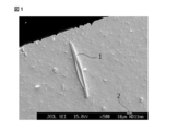
- FIG. 1 is a scanning electron micrograph showing a state in which an intermetallic compound structure is formed in the cross-section of the solder after reflow.
- the solder paste obtained in Comparative Example 5 was used. The observation result of the sample is shown. 1 indicates the intermetallic compound structure that appears in the solder after reflow, and the intermetallic compound structure and the entire periphery thereof indicate the solder portion after reflowing.
- the length of the white line indicated by reference numeral 2 corresponds to an actual length of 10 ⁇ m.
- ⁇ Void suppression> The solder paste obtained in each example and each comparative example was printed on a printed circuit board for chip component mounting, and the chip component was mounted by a reflow method.
- the printed film thickness of the solder paste was adjusted using a metal mask having a thickness of 150 ⁇ m.
- a chip component having a 2012 size (20 mm ⁇ 12 mm) was mounted on a predetermined position of the printed circuit board and heated in a reflow furnace to mount the chip component.
- the reflow conditions were set such that the preheating was 170 to 190 ° C., the peak temperature was 245 ° C., the time of 220 ° C. or higher was 45 seconds, and the cooling rate when the temperature was lowered from the peak temperature to 200 ° C. was 3 to 8 ° C./second.
- the surface state of the solder on the printed circuit board was observed with an X-ray photograph, and the ratio of the total area of voids (area ratio of voids) in the area where the solder was formed was measured.
- the occurrence of voids was evaluated according to the following criteria by calculating the average value of the void area ratio in 20 lands in the printed circuit board.
- A The average value of the void area ratio was 5% or less, and the effect of suppressing the generation of voids was extremely good.
- the operation of immersing the comb substrate in molten solder was repeated, and the number of immersions until the size of the copper wiring of the comb substrate was halved was measured. Considering the reliability of the electronic circuit, the size of the copper wiring must not be halved even if the number of immersions is 4 times or more.
- the case where the number of immersions was 4 times and was not halved was evaluated as “A”, and the case where the number of immersions was halved at 3 times or less was evaluated as “C”.
- the solder paste obtained in each example and each comparative example was printed on a printed circuit board for chip component mounting, and the chip component was mounted by a reflow method.
- the printed film thickness of the solder paste was adjusted using a metal mask having a thickness of 150 ⁇ m.
- a chip component of 3216 size 32 mm ⁇ 16 mm was mounted on a predetermined position of the printed circuit board and heated in a reflow furnace to mount the chip component.
- the reflow conditions were a preheat of 170 to 190 ° C., a peak temperature of 245 ° C. and a time of 220 ° C. or higher for 45 seconds, and a cooling rate when the temperature was lowered from the peak temperature to 200 ° C. was set to 3 to 8 ° C./second.
- the printed circuit board was held for 30 minutes in an environment of ⁇ 40 ° C., and then subjected to a thermal cycle test in which it was held for 30 minutes in an environment of 125 ° C.
- the solder part was cut and the cross section was polished.
- the cross section after polishing was observed with an X-ray photograph to evaluate whether or not a crack generated in the solder fillet portion completely crossed the fillet portion, and was ranked according to the following criteria.
- the number of evaluation chips in each cycle was 20.
- A- A crack that completely traverses the fillet occurred between 2501 and 2750 cycles.
- a + Very good (total score is 10 points or more and does not include items below evaluation “B”)
- A: Good total score is 8 points or more, does not include “D” or lower in the “durability (solder life)” item, and does not include “B-” or lower item
- A- Almost good (total score is 8 points or more and does not include items below evaluation “B-”. Except for items with overall evaluation “A” above)
- solder alloy and the solder paste of the present invention are used in an electronic circuit board used for an electric / electronic device or the like.
Landscapes
- Engineering & Computer Science (AREA)
- Chemical & Material Sciences (AREA)
- Mechanical Engineering (AREA)
- Microelectronics & Electronic Packaging (AREA)
- Manufacturing & Machinery (AREA)
- Materials Engineering (AREA)
- Metallurgy (AREA)
- Organic Chemistry (AREA)
- Dispersion Chemistry (AREA)
- Electric Connection Of Electric Components To Printed Circuits (AREA)
Applications Claiming Priority (2)
| Application Number | Priority Date | Filing Date | Title |
|---|---|---|---|
| JP2012160239 | 2012-07-19 | ||
| JP2012-160239 | 2012-07-19 |
Publications (1)
| Publication Number | Publication Date |
|---|---|
| WO2014013632A1 true WO2014013632A1 (ja) | 2014-01-23 |
Family
ID=49764936
Family Applications (2)
| Application Number | Title | Priority Date | Filing Date |
|---|---|---|---|
| PCT/JP2012/079846 WO2014013632A1 (ja) | 2012-07-19 | 2012-11-16 | はんだ合金、ソルダペーストおよび電子回路基板 |
| PCT/JP2013/067392 WO2014013847A1 (ja) | 2012-07-19 | 2013-06-25 | はんだ合金、ソルダペーストおよび電子回路基板 |
Family Applications After (1)
| Application Number | Title | Priority Date | Filing Date |
|---|---|---|---|
| PCT/JP2013/067392 WO2014013847A1 (ja) | 2012-07-19 | 2013-06-25 | はんだ合金、ソルダペーストおよび電子回路基板 |
Country Status (9)
| Country | Link |
|---|---|
| US (1) | US9445508B2 (zh) |
| EP (2) | EP2875898B1 (zh) |
| JP (1) | JP5349703B1 (zh) |
| KR (1) | KR101538293B1 (zh) |
| CN (3) | CN107052611A (zh) |
| ES (1) | ES2672511T3 (zh) |
| MY (1) | MY154604A (zh) |
| TW (1) | TWI583800B (zh) |
| WO (2) | WO2014013632A1 (zh) |
Cited By (1)
| Publication number | Priority date | Publication date | Assignee | Title |
|---|---|---|---|---|
| JP5638174B1 (ja) * | 2014-06-24 | 2014-12-10 | ハリマ化成株式会社 | はんだ合金、はんだ組成物、ソルダペーストおよび電子回路基板 |
Families Citing this family (37)
| Publication number | Priority date | Publication date | Assignee | Title |
|---|---|---|---|---|
| JP2015077601A (ja) * | 2013-04-02 | 2015-04-23 | 千住金属工業株式会社 | 鉛フリーはんだ合金 |
| US10322471B2 (en) * | 2014-07-21 | 2019-06-18 | Alpha Assembly Solutions Inc. | Low temperature high reliability alloy for solder hierarchy |
| JP6200534B2 (ja) * | 2015-03-24 | 2017-09-20 | 株式会社タムラ製作所 | 鉛フリーはんだ合金、電子回路基板および電子制御装置 |
| JP2016010818A (ja) * | 2015-03-24 | 2016-01-21 | 株式会社タムラ製作所 | 鉛フリーはんだ合金含有ソルダペースト組成物、はんだ接合体構造および電子回路基板 |
| CN106001978B (zh) * | 2015-03-24 | 2020-02-07 | 株式会社田村制作所 | 无铅软钎料合金、电子电路基板和电子控制装置 |
| EP3838473A1 (en) * | 2015-05-05 | 2021-06-23 | Indium Corporation | High reliability lead-free solder alloys for harsh environment electronics applications |
| MY186064A (en) * | 2015-05-05 | 2021-06-18 | Indium Corp | High reliability lead-free solder alloys for harsh environment electronics applications |
| JP6135885B2 (ja) * | 2015-05-19 | 2017-05-31 | パナソニックIpマネジメント株式会社 | はんだ合金およびそれを用いた実装構造体 |
| WO2017018167A1 (ja) | 2015-07-24 | 2017-02-02 | ハリマ化成株式会社 | はんだ合金、ソルダペーストおよび電子回路基板 |
| JP6536306B2 (ja) * | 2015-09-10 | 2019-07-03 | 千住金属工業株式会社 | 鉛フリーはんだ合金と車載電子回路 |
| JP6125084B1 (ja) * | 2016-11-17 | 2017-05-10 | 株式会社タムラ製作所 | 鉛フリーはんだ合金を用いたソルダペースト組成物、電子回路基板および電子制御装置 |
| CN108500499B (zh) | 2016-03-22 | 2019-10-22 | 株式会社田村制作所 | 无铅软钎料合金、电子电路基板和电子控制装置 |
| JP6047254B1 (ja) * | 2016-03-22 | 2016-12-21 | 株式会社タムラ製作所 | 鉛フリーはんだ合金、電子回路基板および電子制御装置 |
| JP6745453B2 (ja) * | 2016-05-18 | 2020-08-26 | パナソニックIpマネジメント株式会社 | はんだ合金およびそれを用いた実装構造体 |
| US20180102464A1 (en) * | 2016-10-06 | 2018-04-12 | Alpha Assembly Solutions Inc. | Advanced Solder Alloys For Electronic Interconnects |
| WO2018134673A1 (ja) | 2017-01-20 | 2018-07-26 | レノボ・シンガポール・プライベート・リミテッド | はんだ接合方法、およびはんだ継手 |
| JP6230737B1 (ja) * | 2017-03-10 | 2017-11-15 | 株式会社タムラ製作所 | 鉛フリーはんだ合金、ソルダペースト及び電子回路基板 |
| HUE056341T2 (hu) | 2017-03-31 | 2022-02-28 | Senju Metal Industry Co | Forrasztóötvözet, forrasztópaszta és forrasztási kötés |
| JP6397079B1 (ja) * | 2017-04-07 | 2018-09-26 | 株式会社ケーヒン | はんだ材料 |
| KR102286739B1 (ko) * | 2017-08-17 | 2021-08-05 | 현대자동차 주식회사 | 무연 솔더 조성물 |
| US10456872B2 (en) | 2017-09-08 | 2019-10-29 | Tamura Corporation | Lead-free solder alloy, electronic circuit substrate, and electronic device |
| JP6349615B1 (ja) * | 2017-10-03 | 2018-07-04 | 株式会社弘輝 | はんだ合金、はんだ接合材料及び電子回路基板 |
| JP6467484B2 (ja) * | 2017-10-13 | 2019-02-13 | 株式会社タムラ製作所 | 鉛フリーはんだ合金、電子回路基板および電子制御装置 |
| JP6275318B1 (ja) * | 2017-10-13 | 2018-02-07 | 株式会社タムラ製作所 | 鉛フリーはんだ合金、電子回路基板および電子制御装置 |
| JP6467485B2 (ja) * | 2017-10-17 | 2019-02-13 | 株式会社タムラ製作所 | 鉛フリーはんだ合金、電子回路基板および電子制御装置 |
| JP2018171656A (ja) * | 2018-05-28 | 2018-11-08 | 千住金属工業株式会社 | 鉛フリーはんだ合金と車載電子回路 |
| JP6796108B2 (ja) * | 2018-06-04 | 2020-12-02 | 株式会社タムラ製作所 | 鉛フリーはんだ合金、ソルダペースト、電子回路実装基板及び電子制御装置 |
| JP2019072770A (ja) * | 2018-12-05 | 2019-05-16 | 千住金属工業株式会社 | 鉛フリーはんだ合金と車載電子回路 |
| JP6731034B2 (ja) | 2018-12-25 | 2020-07-29 | 株式会社タムラ製作所 | 鉛フリーはんだ合金、はんだ接合用材料、電子回路実装基板及び電子制御装置 |
| JP6795630B2 (ja) * | 2019-01-10 | 2020-12-02 | 株式会社タムラ製作所 | 鉛フリーはんだ合金、ソルダペースト組成物、電子回路基板および電子制御装置 |
| JP6624322B1 (ja) | 2019-03-27 | 2019-12-25 | 千住金属工業株式会社 | はんだ合金、はんだボール、はんだプリフォーム、はんだペースト及びはんだ継手 |
| CN113874158B (zh) * | 2019-05-27 | 2022-12-13 | 千住金属工业株式会社 | 焊料合金、焊膏、焊球、焊料预制件、焊接接头 |
| JP6700568B1 (ja) * | 2019-08-09 | 2020-05-27 | 千住金属工業株式会社 | 鉛フリーかつアンチモンフリーのはんだ合金、はんだボール、Ball Grid Arrayおよびはんだ継手 |
| TWI714420B (zh) * | 2020-01-06 | 2020-12-21 | 昇貿科技股份有限公司 | 無鉛無銅錫合金與用於球柵陣列封裝的錫球 |
| JP7066806B2 (ja) * | 2020-11-13 | 2022-05-13 | 株式会社タムラ製作所 | 鉛フリーはんだ合金、ソルダペースト、電子回路実装基板及び電子制御装置 |
| JP7161134B1 (ja) | 2021-09-30 | 2022-10-26 | 千住金属工業株式会社 | はんだ合金、はんだボール、はんだプリフォーム、はんだペースト及びはんだ継手 |
| JP7161133B1 (ja) | 2021-09-30 | 2022-10-26 | 千住金属工業株式会社 | はんだ合金、はんだボール、はんだプリフォーム、はんだペースト及びはんだ継手 |
Citations (5)
| Publication number | Priority date | Publication date | Assignee | Title |
|---|---|---|---|---|
| WO2006059115A1 (en) * | 2004-12-01 | 2006-06-08 | Alpha Fry Limited | Solder alloy |
| WO2006131979A1 (ja) * | 2005-06-10 | 2006-12-14 | Senju Metal Industry Co., Ltd. | 無電解Niめっき部のはんだ付け方法 |
| WO2009011341A1 (ja) * | 2007-07-13 | 2009-01-22 | Senju Metal Industry Co., Ltd. | 車載実装用鉛フリーはんだと車載電子回路 |
| WO2009011392A1 (ja) * | 2007-07-18 | 2009-01-22 | Senju Metal Industry Co., Ltd. | 車載電子回路用In入り鉛フリーはんだ |
| WO2010122764A1 (ja) * | 2009-04-20 | 2010-10-28 | パナソニック株式会社 | はんだ材料および電子部品接合体 |
Family Cites Families (19)
| Publication number | Priority date | Publication date | Assignee | Title |
|---|---|---|---|---|
| JP2000015476A (ja) | 1998-06-29 | 2000-01-18 | Ishikawa Kinzoku Kk | 無鉛はんだ |
| KR20010072364A (ko) * | 1999-06-11 | 2001-07-31 | 이즈하라 요조 | 무연 땜납 |
| JP2001071131A (ja) | 1999-09-01 | 2001-03-21 | Sanshin Kinzoku Kogyo Kk | 定尺金属成形材の製造設備 |
| JP2001071173A (ja) | 1999-09-06 | 2001-03-21 | Ishikawa Kinzoku Kk | 無鉛はんだ |
| JP2002096191A (ja) | 2000-09-18 | 2002-04-02 | Matsushita Electric Ind Co Ltd | はんだ材料およびこれを利用する電気・電子機器 |
| JP2004141910A (ja) * | 2002-10-23 | 2004-05-20 | Senju Metal Ind Co Ltd | 鉛フリーはんだ合金 |
| DE10319888A1 (de) | 2003-04-25 | 2004-11-25 | Siemens Ag | Lotmaterial auf SnAgCu-Basis |
| US8691143B2 (en) | 2005-06-03 | 2014-04-08 | Senju Metal Industry Co., Ltd. | Lead-free solder alloy |
| US20080159904A1 (en) * | 2005-08-24 | 2008-07-03 | Fry's Metals, Inc. | Solder alloy |
| US8641964B2 (en) | 2005-08-24 | 2014-02-04 | Fry's Metals, Inc. | Solder alloy |
| KR20130073995A (ko) | 2006-03-09 | 2013-07-03 | 신닛테츠스미킹 마테리알즈 가부시키가이샤 | 무연 솔더 합금, 솔더 볼 및 전자 부재와, 자동차 탑재 전자 부재용 무연 솔더 합금, 솔더 볼 및 전자 부재 |
| CN101848787B (zh) * | 2007-08-14 | 2013-10-23 | 株式会社爱科草英 | 无铅焊料组合物及使用它的印刷电路板与电子器件 |
| WO2009051181A1 (ja) | 2007-10-19 | 2009-04-23 | Nihon Superior Sha Co., Ltd. | 無鉛はんだ合金 |
| CN102066043B (zh) | 2008-04-23 | 2014-05-07 | 千住金属工业株式会社 | 抑制缩孔的无铅焊料合金 |
| TW201016373A (en) | 2008-10-16 | 2010-05-01 | Nihon Superior Co Ltd | Lead-free solder alloy |
| JP4554713B2 (ja) | 2009-01-27 | 2010-09-29 | 株式会社日本フィラーメタルズ | 無鉛はんだ合金及び該はんだ合金を含む耐疲労性はんだ接合材並びに該接合材を使用した接合体 |
| WO2011102034A1 (ja) * | 2010-02-16 | 2011-08-25 | 株式会社タムラ製作所 | 鉛フリーはんだ合金と、これを用いたソルダペースト及び実装品 |
| JP2012061491A (ja) * | 2010-09-15 | 2012-03-29 | Nippon Genma:Kk | 鉛フリーはんだ合金 |
| JP4787384B1 (ja) * | 2010-10-29 | 2011-10-05 | ハリマ化成株式会社 | 低銀はんだ合金およびはんだペースト組成物 |
-
2012
- 2012-11-16 WO PCT/JP2012/079846 patent/WO2014013632A1/ja active Application Filing
-
2013
- 2013-02-18 JP JP2013029247A patent/JP5349703B1/ja active Active
- 2013-06-25 CN CN201710413832.XA patent/CN107052611A/zh active Pending
- 2013-06-25 MY MYPI2015000067A patent/MY154604A/en unknown
- 2013-06-25 US US14/414,453 patent/US9445508B2/en active Active
- 2013-06-25 EP EP13819569.8A patent/EP2875898B1/en active Active
- 2013-06-25 EP EP17181894.1A patent/EP3257617A1/en not_active Withdrawn
- 2013-06-25 WO PCT/JP2013/067392 patent/WO2014013847A1/ja active Application Filing
- 2013-06-25 KR KR1020157001004A patent/KR101538293B1/ko active IP Right Grant
- 2013-06-25 ES ES13819569.8T patent/ES2672511T3/es active Active
- 2013-06-25 CN CN201710413403.2A patent/CN107214430B/zh active Active
- 2013-06-25 CN CN201380037553.8A patent/CN104507633A/zh active Pending
- 2013-07-18 TW TW102125695A patent/TWI583800B/zh active
Patent Citations (5)
| Publication number | Priority date | Publication date | Assignee | Title |
|---|---|---|---|---|
| WO2006059115A1 (en) * | 2004-12-01 | 2006-06-08 | Alpha Fry Limited | Solder alloy |
| WO2006131979A1 (ja) * | 2005-06-10 | 2006-12-14 | Senju Metal Industry Co., Ltd. | 無電解Niめっき部のはんだ付け方法 |
| WO2009011341A1 (ja) * | 2007-07-13 | 2009-01-22 | Senju Metal Industry Co., Ltd. | 車載実装用鉛フリーはんだと車載電子回路 |
| WO2009011392A1 (ja) * | 2007-07-18 | 2009-01-22 | Senju Metal Industry Co., Ltd. | 車載電子回路用In入り鉛フリーはんだ |
| WO2010122764A1 (ja) * | 2009-04-20 | 2010-10-28 | パナソニック株式会社 | はんだ材料および電子部品接合体 |
Cited By (5)
| Publication number | Priority date | Publication date | Assignee | Title |
|---|---|---|---|---|
| JP5638174B1 (ja) * | 2014-06-24 | 2014-12-10 | ハリマ化成株式会社 | はんだ合金、はんだ組成物、ソルダペーストおよび電子回路基板 |
| KR101551613B1 (ko) | 2014-06-24 | 2015-09-08 | 하리마카세이 가부시기가이샤 | 땜납 합금, 땜납 조성물, 솔더 페이스트 및 전자 회로 기판 |
| WO2015198496A1 (ja) * | 2014-06-24 | 2015-12-30 | ハリマ化成株式会社 | はんだ合金、はんだ組成物、ソルダペーストおよび電子回路基板 |
| US9931716B2 (en) | 2014-06-24 | 2018-04-03 | Harima Chemicals, Incorporated | Solder alloy, solder composition, solder paste, and electronic circuit board |
| US9956649B2 (en) | 2014-06-24 | 2018-05-01 | Harima Chemicals, Incorporated | Solder alloy, solder paste, and electronic circuit board |
Also Published As
| Publication number | Publication date |
|---|---|
| MY154604A (en) | 2015-07-01 |
| TW201408787A (zh) | 2014-03-01 |
| WO2014013847A1 (ja) | 2014-01-23 |
| TWI583800B (zh) | 2017-05-21 |
| CN107214430B (zh) | 2022-06-28 |
| CN104507633A (zh) | 2015-04-08 |
| CN107214430A (zh) | 2017-09-29 |
| JP2014037005A (ja) | 2014-02-27 |
| ES2672511T3 (es) | 2018-06-14 |
| CN107052611A (zh) | 2017-08-18 |
| EP2875898B1 (en) | 2018-03-28 |
| KR20150029705A (ko) | 2015-03-18 |
| EP2875898A1 (en) | 2015-05-27 |
| EP3257617A1 (en) | 2017-12-20 |
| EP2875898A4 (en) | 2016-07-06 |
| KR101538293B1 (ko) | 2015-07-20 |
| US9445508B2 (en) | 2016-09-13 |
| JP5349703B1 (ja) | 2013-11-20 |
| US20150305167A1 (en) | 2015-10-22 |
Similar Documents
| Publication | Publication Date | Title |
|---|---|---|
| JP5349703B1 (ja) | はんだ合金、ソルダペーストおよび電子回路基板 | |
| JP5238088B1 (ja) | はんだ合金、ソルダペーストおよび電子回路基板 | |
| JP5638174B1 (ja) | はんだ合金、はんだ組成物、ソルダペーストおよび電子回路基板 | |
| JP5324007B1 (ja) | はんだ合金、ソルダペーストおよび電子回路基板 | |
| JP5730354B2 (ja) | はんだ組成物、ソルダペーストおよび電子回路基板 | |
| KR102566561B1 (ko) | 땜납 합금, 솔더 페이스트 및 전자 회로 기판 | |
| JP2012106280A (ja) | 低銀はんだ合金およびはんだペースト組成物 | |
| JP5654716B1 (ja) | はんだ合金、ソルダペーストおよび電子回路基板 |
Legal Events
| Date | Code | Title | Description |
|---|---|---|---|
| 121 | Ep: the epo has been informed by wipo that ep was designated in this application |
Ref document number: 12881244 Country of ref document: EP Kind code of ref document: A1 |
|
| NENP | Non-entry into the national phase |
Ref country code: DE |
|
| 122 | Ep: pct application non-entry in european phase |
Ref document number: 12881244 Country of ref document: EP Kind code of ref document: A1 |