WO2013099492A1 - 色素増感太陽電池 - Google Patents
色素増感太陽電池 Download PDFInfo
- Publication number
- WO2013099492A1 WO2013099492A1 PCT/JP2012/080606 JP2012080606W WO2013099492A1 WO 2013099492 A1 WO2013099492 A1 WO 2013099492A1 JP 2012080606 W JP2012080606 W JP 2012080606W WO 2013099492 A1 WO2013099492 A1 WO 2013099492A1
- Authority
- WO
- WIPO (PCT)
- Prior art keywords
- group
- dye
- optionally substituted
- atom
- hydrocarbon group
- Prior art date
- Legal status (The legal status is an assumption and is not a legal conclusion. Google has not performed a legal analysis and makes no representation as to the accuracy of the status listed.)
- Ceased
Links
- CYVJETAPYINMAB-LZWSPWQCSA-N C/C=C(\C(CC=O)=C1C)/c2c3c1cccc3ccc2 Chemical compound C/C=C(\C(CC=O)=C1C)/c2c3c1cccc3ccc2 CYVJETAPYINMAB-LZWSPWQCSA-N 0.000 description 1
Images


Classifications
-
- H—ELECTRICITY
- H01—ELECTRIC ELEMENTS
- H01G—CAPACITORS; CAPACITORS, RECTIFIERS, DETECTORS, SWITCHING DEVICES, LIGHT-SENSITIVE OR TEMPERATURE-SENSITIVE DEVICES OF THE ELECTROLYTIC TYPE
- H01G9/00—Electrolytic capacitors, rectifiers, detectors, switching devices, light-sensitive or temperature-sensitive devices; Processes of their manufacture
- H01G9/20—Light-sensitive devices
- H01G9/2027—Light-sensitive devices comprising an oxide semiconductor electrode
- H01G9/204—Light-sensitive devices comprising an oxide semiconductor electrode comprising zinc oxides, e.g. ZnO
-
- C—CHEMISTRY; METALLURGY
- C07—ORGANIC CHEMISTRY
- C07F—ACYCLIC, CARBOCYCLIC OR HETEROCYCLIC COMPOUNDS CONTAINING ELEMENTS OTHER THAN CARBON, HYDROGEN, HALOGEN, OXYGEN, NITROGEN, SULFUR, SELENIUM OR TELLURIUM
- C07F15/00—Compounds containing elements of Groups 8, 9, 10 or 18 of the Periodic Table
- C07F15/0006—Compounds containing elements of Groups 8, 9, 10 or 18 of the Periodic Table compounds of the platinum group
- C07F15/0046—Ruthenium compounds
- C07F15/0053—Ruthenium compounds without a metal-carbon linkage
-
- C—CHEMISTRY; METALLURGY
- C07—ORGANIC CHEMISTRY
- C07F—ACYCLIC, CARBOCYCLIC OR HETEROCYCLIC COMPOUNDS CONTAINING ELEMENTS OTHER THAN CARBON, HYDROGEN, HALOGEN, OXYGEN, NITROGEN, SULFUR, SELENIUM OR TELLURIUM
- C07F17/00—Metallocenes
- C07F17/02—Metallocenes of metals of Groups 8, 9 or 10 of the Periodic Table
-
- C—CHEMISTRY; METALLURGY
- C07—ORGANIC CHEMISTRY
- C07F—ACYCLIC, CARBOCYCLIC OR HETEROCYCLIC COMPOUNDS CONTAINING ELEMENTS OTHER THAN CARBON, HYDROGEN, HALOGEN, OXYGEN, NITROGEN, SULFUR, SELENIUM OR TELLURIUM
- C07F7/00—Compounds containing elements of Groups 4 or 14 of the Periodic Table
- C07F7/02—Silicon compounds
- C07F7/08—Compounds having one or more C—Si linkages
- C07F7/18—Compounds having one or more C—Si linkages as well as one or more C—O—Si linkages
- C07F7/1804—Compounds having Si-O-C linkages
-
- C—CHEMISTRY; METALLURGY
- C09—DYES; PAINTS; POLISHES; NATURAL RESINS; ADHESIVES; COMPOSITIONS NOT OTHERWISE PROVIDED FOR; APPLICATIONS OF MATERIALS NOT OTHERWISE PROVIDED FOR
- C09B—ORGANIC DYES OR CLOSELY-RELATED COMPOUNDS FOR PRODUCING DYES, e.g. PIGMENTS; MORDANTS; LAKES
- C09B69/00—Dyes not provided for by a single group of this subclass
- C09B69/008—Dyes containing a substituent, which contains a silicium atom
-
- H—ELECTRICITY
- H01—ELECTRIC ELEMENTS
- H01G—CAPACITORS; CAPACITORS, RECTIFIERS, DETECTORS, SWITCHING DEVICES, LIGHT-SENSITIVE OR TEMPERATURE-SENSITIVE DEVICES OF THE ELECTROLYTIC TYPE
- H01G9/00—Electrolytic capacitors, rectifiers, detectors, switching devices, light-sensitive or temperature-sensitive devices; Processes of their manufacture
- H01G9/20—Light-sensitive devices
- H01G9/2027—Light-sensitive devices comprising an oxide semiconductor electrode
- H01G9/2031—Light-sensitive devices comprising an oxide semiconductor electrode comprising titanium oxide, e.g. TiO2
-
- H—ELECTRICITY
- H01—ELECTRIC ELEMENTS
- H01G—CAPACITORS; CAPACITORS, RECTIFIERS, DETECTORS, SWITCHING DEVICES, LIGHT-SENSITIVE OR TEMPERATURE-SENSITIVE DEVICES OF THE ELECTROLYTIC TYPE
- H01G9/00—Electrolytic capacitors, rectifiers, detectors, switching devices, light-sensitive or temperature-sensitive devices; Processes of their manufacture
- H01G9/20—Light-sensitive devices
- H01G9/2059—Light-sensitive devices comprising an organic dye as the active light absorbing material, e.g. adsorbed on an electrode or dissolved in solution
-
- H—ELECTRICITY
- H10—SEMICONDUCTOR DEVICES; ELECTRIC SOLID-STATE DEVICES NOT OTHERWISE PROVIDED FOR
- H10K—ORGANIC ELECTRIC SOLID-STATE DEVICES
- H10K85/00—Organic materials used in the body or electrodes of devices covered by this subclass
- H10K85/40—Organosilicon compounds, e.g. TIPS pentacene
-
- H—ELECTRICITY
- H10—SEMICONDUCTOR DEVICES; ELECTRIC SOLID-STATE DEVICES NOT OTHERWISE PROVIDED FOR
- H10K—ORGANIC ELECTRIC SOLID-STATE DEVICES
- H10K85/00—Organic materials used in the body or electrodes of devices covered by this subclass
- H10K85/60—Organic compounds having low molecular weight
- H10K85/649—Aromatic compounds comprising a hetero atom
- H10K85/652—Cyanine dyes
-
- H—ELECTRICITY
- H10—SEMICONDUCTOR DEVICES; ELECTRIC SOLID-STATE DEVICES NOT OTHERWISE PROVIDED FOR
- H10K—ORGANIC ELECTRIC SOLID-STATE DEVICES
- H10K85/00—Organic materials used in the body or electrodes of devices covered by this subclass
- H10K85/30—Coordination compounds
- H10K85/341—Transition metal complexes, e.g. Ru(II)polypyridine complexes
- H10K85/344—Transition metal complexes, e.g. Ru(II)polypyridine complexes comprising ruthenium
-
- H—ELECTRICITY
- H10—SEMICONDUCTOR DEVICES; ELECTRIC SOLID-STATE DEVICES NOT OTHERWISE PROVIDED FOR
- H10K—ORGANIC ELECTRIC SOLID-STATE DEVICES
- H10K85/00—Organic materials used in the body or electrodes of devices covered by this subclass
- H10K85/30—Coordination compounds
- H10K85/371—Metal complexes comprising a group IB metal element, e.g. comprising copper, gold or silver
-
- H—ELECTRICITY
- H10—SEMICONDUCTOR DEVICES; ELECTRIC SOLID-STATE DEVICES NOT OTHERWISE PROVIDED FOR
- H10K—ORGANIC ELECTRIC SOLID-STATE DEVICES
- H10K85/00—Organic materials used in the body or electrodes of devices covered by this subclass
- H10K85/30—Coordination compounds
- H10K85/381—Metal complexes comprising a group IIB metal element, e.g. comprising cadmium, mercury or zinc
-
- Y—GENERAL TAGGING OF NEW TECHNOLOGICAL DEVELOPMENTS; GENERAL TAGGING OF CROSS-SECTIONAL TECHNOLOGIES SPANNING OVER SEVERAL SECTIONS OF THE IPC; TECHNICAL SUBJECTS COVERED BY FORMER USPC CROSS-REFERENCE ART COLLECTIONS [XRACs] AND DIGESTS
- Y02—TECHNOLOGIES OR APPLICATIONS FOR MITIGATION OR ADAPTATION AGAINST CLIMATE CHANGE
- Y02E—REDUCTION OF GREENHOUSE GAS [GHG] EMISSIONS, RELATED TO ENERGY GENERATION, TRANSMISSION OR DISTRIBUTION
- Y02E10/00—Energy generation through renewable energy sources
- Y02E10/50—Photovoltaic [PV] energy
- Y02E10/542—Dye sensitized solar cells
-
- Y—GENERAL TAGGING OF NEW TECHNOLOGICAL DEVELOPMENTS; GENERAL TAGGING OF CROSS-SECTIONAL TECHNOLOGIES SPANNING OVER SEVERAL SECTIONS OF THE IPC; TECHNICAL SUBJECTS COVERED BY FORMER USPC CROSS-REFERENCE ART COLLECTIONS [XRACs] AND DIGESTS
- Y02—TECHNOLOGIES OR APPLICATIONS FOR MITIGATION OR ADAPTATION AGAINST CLIMATE CHANGE
- Y02E—REDUCTION OF GREENHOUSE GAS [GHG] EMISSIONS, RELATED TO ENERGY GENERATION, TRANSMISSION OR DISTRIBUTION
- Y02E10/00—Energy generation through renewable energy sources
- Y02E10/50—Photovoltaic [PV] energy
- Y02E10/549—Organic PV cells
Definitions
- the present invention relates to a dye-sensitized solar cell using an oxide semiconductor layer containing a sensitizing dye having a specific structure in a dye-sensitized solar cell having a basic compound in an electrolyte-containing layer or a solid charge transfer layer.
- Dye-sensitized solar cells are (1) the cost of manufacturing is expected to be 1/5 to 1/10 that of silicon solar cells, and are inexpensive. (2) CO 2 emissions during production The amount is less than 1/10 of single crystal silicon solar cells, and is small, (3) Energy payback time or CO 2 payback time is less than half that of polycrystalline silicon solar cells, and short, (4) Resource constraints on raw materials Excellent features such as (5) excellent design and workability, easy to enlarge, (6) relatively high photoelectric conversion efficiency of 10% or more comparable to amorphous silicon solar cells. Therefore, development research is actively promoted as a next-generation solar cell that replaces the silicon-based solar cell.
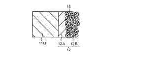
- FIG. 3 and FIG. 4 schematically show a cross-sectional configuration of an example of a conventional dye-sensitized solar cell
- FIG. 2 extracts the main part of the dye-sensitized solar cell shown in FIG. It is shown enlarged.
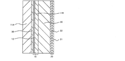
- a working electrode 10 made of a substrate 11A on which a conductive layer 11B and a metal oxide semiconductor layer 12 are laminated and a counter electrode 20 are arranged to face each other with an electrolyte-containing layer 30 interposed therebetween.
- at least one of the working electrode 10 and the counter electrode 20 is an electrode having optical transparency.
- Non-patent Documents 1 and 2 are attracting attention because the conductive layer 11B need not be transparent if the substrate 11A is transparent, and can be manufactured at low cost. In the case of taking the configuration of FIG. 3 or FIG. 4, it is necessary to use a conductive layer 11B that can permeate a porous or lattice electrolyte component (Non-patent Documents 1 and 2).
- the dye-sensitized solar cell is composed of a working electrode (photoelectric conversion element) 10 and a counter electrode 20, and an electrolyte-containing layer (electrolyte) 30 portion sandwiched between the two electrodes.
- the working electrode 10 is formed by applying and baking nano-sized metal oxide semiconductor particles 12B on the conductive layer side on which the conductive layer 11B is formed on the surface of the substrate 11A such as glass to form the metal oxide semiconductor layer 12. It is produced by immobilizing the dye 13 on the metal oxide semiconductor particles by chemical and physical adsorption.
- the counter electrode 20 has a conductive layer 22 formed on the surface of a base material 21 such as glass, and is produced by performing a catalytic amount of platinum treatment or conductive carbon treatment on the conductive layer side.
- the working electrode 10 and the counter electrode 20 are overlapped, and an electrolyte composition containing the iodine compound (electrolyte-containing layer 30) is injected between the electrodes 10 and 20, thereby producing a solar cell.
- the power generation mechanism of the dye-sensitized solar cell is that electrons are injected from the sensitizing dye excited by sunlight (visible light) irradiation into the conduction band of the metal oxide semiconductor, and the injected electrons are externally transmitted through the photoelectrode. It is guided to the circuit and moves to the counter electrode, and the sensitizing dye (dye cation) in the oxidized state receives electrons and regenerates through the redox reaction of the electrolyte composition. This cycle achieves photoelectric conversion.
- the dye-sensitized solar cell has not been put into practical use because it has a lower photoelectric conversion efficiency than silicon-based solar cells that are currently on the market.
- the main cause of the decrease in photoelectric conversion efficiency of dye-sensitized solar cells is a decrease in voltage due to reverse electron transfer from the oxide semiconductor layer to the electrolyte composition and dye cation, in order to suppress reverse electron transfer and prevent voltage drop
- the addition of a basic compound to the electrolyte composition has been studied.
- an object of the present invention is to provide a dye-sensitized solar cell that can suppress desorption of a sensitizing dye even when an electrolyte-containing layer or a solid charge transfer layer containing a basic compound is used.
- the present inventors have found a combination of a dye compound having a specific structure and a basic compound, and have found that such a combination can achieve the above-described object, leading to the present invention.
- the present invention is a dye-sensitized solar cell comprising a working electrode having a photocatalytic film, a counter electrode, an electrolyte-containing layer or a solid charge transfer layer, Dye sensitization characterized in that the electrolyte-containing layer or the solid charge transfer layer contains a basic compound and the photocatalytic film is formed of an oxide semiconductor layer containing a dye compound represented by the following general formula (1).
- a solar cell is provided.
- Y is a hydrocarbon group having 1 to 20 carbon atoms which may have a —CO—NR 4 — or —SO 2 —NR 4 — in the group or a direct bond;
- a conjugated group wherein R 1 , R 2 and R 3 each represents an optionally substituted hydrocarbon group or an optionally substituted hydrocarbon oxy group, and at least one of R 1 , R 2 and R 3 ;
- R 4 represents a hydrogen atom or a hydrocarbon group having 1 to 20 carbon atoms which may have a substituent.
- the sensitizing dye has a silyl group in which a hydrocarbon oxy group and Si are bonded. Thus, it has excellent adsorptivity to the metal oxide semiconductor. Moreover, since the adsorptivity is high, the dye-sensitized solar cell of the present invention is a highly efficient and highly durable element.
- FIG. 1 is a schematic diagram showing a cross-sectional configuration of an example of a conventional dye-sensitized solar cell.
- FIG. 2 is an enlarged view of a main part of the dye-sensitized solar cell shown in FIG.
- FIG. 3 is a schematic diagram showing a cross-sectional configuration of another example of a conventional dye-sensitized solar cell.
- FIG. 4 is a schematic diagram showing a cross-sectional configuration of still another example of a conventional dye-sensitized solar cell.
- the configuration itself of the dye-sensitized solar cell of the present invention is not particularly limited as long as it includes a working electrode having a photocatalytic film, a counter electrode, and an electrolyte-containing layer.
- the dye 13 carried on the working electrode 10 when light (sunlight or ultraviolet light, visible light, or near-infrared light equivalent to sunlight) is applied to the dye 13 carried on the working electrode 10, the light is emitted.
- the dye 13 excited by absorbing the electrons injects electrons into the metal oxide semiconductor layer 12. After the electrons move to the adjacent conductive layer 11B, they reach the counter electrode 20 via an external circuit.
- the electrolyte-containing layer 30 the electrolyte is oxidized so that the oxidized dye 13 is returned (reduced) to the ground state as the electrons move.
- the oxidized electrolyte is reduced by receiving the electrons that have reached the counter electrode 20. In this way, the movement of electrons between the working electrode 10 and the counter electrode 20 and the accompanying oxidation-reduction reaction in the electrolyte-containing layer 30 are repeated. Thereby, continuous movement of electrons occurs, and photoelectric conversion is constantly performed.
- the working electrode 10 will be described.
- the working electrode 10 includes, for example, a conductive substrate 11, a metal oxide semiconductor layer 12 provided on one surface thereof (a surface on the counter electrode 20 side), and a dye 13 supported on the metal oxide semiconductor layer 12. And have.
- the dye 13 is a compound represented by the general formula (1).
- the working electrode 10 functions as a negative electrode for the external circuit.
- the conductive substrate 11 is obtained by providing a conductive layer 11B on the surface of an insulating substrate 11A.
- Examples of the material of the substrate 11A include insulating materials such as glass and plastic.
- the plastic is used, for example, in the form of a transparent polymer film.
- Examples of the plastic forming the transparent polymer film include tetraacetyl cellulose (TAC), polyethylene terephthalate (PET), polyethylene naphthalate (PEN), and syndiotactic polystyrene ( Examples thereof include SPS), polyphenylene sulfide (PPS), polycarbonate (PC), polyarylate (PAR), polysulfone (PSF), polyester sulfone (PES), polyetherimide (PEI), cyclic polyolefin, and brominated phenoxy.
- TAC tetraacetyl cellulose
- PET polyethylene terephthalate
- PEN polyethylene naphthalate
- syndiotactic polystyrene examples thereof include SPS), polyphenylene sulfide (PPS), polycarbonate (
- Examples of the conductive layer 11B include a conductive metal oxide thin film including indium oxide, tin oxide, indium-tin composite oxide (ITO), or tin oxide doped with fluorine (FTO: F—SnO 2 ). , Gold (Au), silver (Ag), platinum (Pt) or the like, a metal thin film and metal mesh, those formed of a conductive polymer, and the like.
- the conductive substrate 11 may be configured to have a single-layer structure with, for example, a conductive material.
- a conductive material examples include indium oxide, tin oxide, Examples thereof include conductive metal oxides such as indium-tin composite oxide or tin oxide doped with fluorine, metals such as gold, silver or platinum, and conductive polymers.
- the metal oxide semiconductor layer 12 is a carrier that supports the dye 13, and has, for example, a porous structure as shown in FIG.
- the metal oxide semiconductor layer 12 is formed of a dense layer 12A and a porous layer 12B.
- the dense layer 12A is formed at the interface with the conductive substrate 11, is preferably dense and has few voids, and more preferably is a film.
- the porous layer 12B is preferably formed on the surface in contact with the electrolyte-containing layer 30, has a large space and a large surface area, and more preferably has a structure in which porous fine particles are attached.
- the metal oxide semiconductor layer 12 may be formed to have, for example, a film-like single layer structure.
- the term “supported” refers to a state in which the dye 13 is chemically or physically or electrically bonded or adsorbed to the porous layer 12B.
- Examples of the material (metal oxide semiconductor material) constituting the metal oxide semiconductor layer 12 include titanium oxide, zinc oxide, tin oxide, niobium oxide, indium oxide, zirconium oxide, tantalum oxide, vanadium oxide, yttrium oxide, and oxide. Aluminum, magnesium oxide, etc. are mentioned. Among these, titanium oxide and zinc oxide are preferable as the metal oxide semiconductor material because high conversion efficiency can be obtained. Further, any one of these metal oxide semiconductor materials may be used alone, or two or more of them may be used in combination (mixed, mixed crystal, solid solution, surface coating, etc.). A combination of titanium oxide and zinc oxide can also be used.
- Examples of the method for forming the metal oxide semiconductor layer 12 having a porous structure include an electrolytic deposition method, a coating method, and a firing method.
- the metal oxide semiconductor layer 12 is formed by electrolytic deposition, the fine particles are deposited on the conductive layer 11B of the conductive substrate 11 in the electrolytic bath liquid containing the fine particles of the metal oxide semiconductor material and the metal.
- An oxide semiconductor material is deposited.
- a dispersion liquid metal oxide slurry
- a dispersion liquid metal oxide slurry in which fine particles of a metal oxide semiconductor material are dispersed is applied on the conductive substrate 11, and then in the dispersion liquid. Dry to remove the dispersion medium.
- the metal oxide semiconductor layer 12 is formed by the sintering method
- the metal oxide slurry is applied onto the conductive substrate 11 and dried, as in the coating method, and then fired.
- the metal oxide semiconductor layer 12 is formed by an electrolytic deposition method or a coating method
- a plastic material or a polymer film material having low heat resistance can be used as the substrate 11A, and thus a highly flexible electrode is manufactured. Can do.
- the metal oxide semiconductor layer 12 may be processed using an organic base, a urea derivative, or a cyclic sugar chain.
- organic base include organic bases such as diarylamine, triarylamine, pyridine, 4-t-butylpyridine, polyvinylpyridine, quinoline, piperidine, and amidine.
- the treatment may be performed before or after adsorbing the dye 13 described below.
- the treatment method includes dipping treatment. When the treatment agent is solid, the dipping treatment may be performed after dissolving in an organic solvent.
- the dye 13 is, for example, adsorbed to the metal oxide semiconductor layer 12, and is capable of injecting electrons into the metal oxide semiconductor layer 12 by absorbing light and being excited. Contains more than one type of dye (sensitizing dye).
- the compound represented by the general formula (1) corresponds to the dye 13.
- the desorption of the dye 13 is suppressed even if the electrolyte-containing layer 30 described later contains a basic compound.
- the compound represented by the general formula (1) used as the dye 13 will be described.
- the group represented by Y in the general formula (1) is a divalent group, and is optionally substituted carbon atom having 1 to 20 carbon atoms and having —CO—NR 4 — or —SO 2 —NR 4 —. It is a hydrogen group or a direct bond.
- the optionally substituted hydrocarbon group include an aliphatic hydrocarbon group, an unsubstituted aromatic hydrocarbon group, an aromatic hydrocarbon group substituted with an aliphatic hydrocarbon group, an unsubstituted heterocyclic group, or an aliphatic carbon group. Examples include a heterocyclic group substituted with a hydrogen group.
- the divalent aliphatic hydrocarbon group is a linear, branched or cyclic aliphatic hydrocarbon group, and specifically includes methane-1,1-diyl, ethane-1,2-diyl, 1- Methylethane-1,2-diyl, propane-1,3-diyl, butane-1,4-diyl, 2-methylpropane-1,3-diyl, pentane-1,5-diyl, hexane-1,6-diyl , Heptane-1,7-diyl, octane-1,8-diyl, nonane-1,9-diyl, decane-1,10-diyl, cyclohexane-1,4-diyl and the like.
- methane-1,1-diyl, ethane-1,2-diyl, and 1-methylethane-1,2-diyl are preferable because the conversion efficiency
- divalent unsubstituted aromatic hydrocarbon group examples include 1,2-phenylene, 1,3-phenylene, 1,4-phenylene and the like.
- divalent unsubstituted heterocyclic group examples include furan-2,5-diyl, furan-3,5-diyl, thiophene-2,5-diyl, thiophene-3,5-diyl, 2H-chromene-3,7. -Diyl, benzothiophene-2,6-diyl or benzothiophene-2,5-diyl.
- divalent aromatic hydrocarbon group substituted with an aliphatic hydrocarbon group and the divalent heterocyclic group substituted with an aliphatic hydrocarbon group include, for example, the above divalent unsubstituted aromatic hydrocarbon group and Examples thereof include those in which a hydrogen atom of an unsubstituted heterocyclic group is substituted by 1 to 3 positions with an aliphatic hydrocarbon group having 1 to 4 carbon atoms.
- Examples of the aliphatic hydrocarbon group having 1 to 4 carbon atoms include straight chain, branched chain, and cyclic such as methyl, ethyl, propyl, isopropyl, butyl, s-butyl, t-butyl, isobutyl, cyclopropyl, and cyclobutyl.
- the aliphatic hydrocarbon group having 1 to 4 carbon atoms includes —O—, —COO—, —OCO—, —CO—, —S—, —SO—, —SO 2 —, May be interrupted by —NR 10 —, —C ⁇ C— or —C ⁇ C—, and R 10 is an aliphatic hydrocarbon group having 1 to 4 carbon atoms.
- the aliphatic hydrocarbon group, aromatic hydrocarbon group or heterocyclic group mentioned above may be further substituted, and the aliphatic hydrocarbon group, aromatic hydrocarbon group and aromatic heterocyclic group may be substituted.
- the preferable group include a fluorine atom, a chlorine atom, a bromine atom, an iodine atom, a cyano group, a nitro group, a hydroxyl group, a thiol group, and a —NR 7 R 8 group.
- R 7 and R 8 represent the same groups as R 7 and R 8 in formulas (A2-1) to (A2-15) described later.
- two hydrogen atoms may be substituted by the same oxygen atom and carbonyl may be sufficient.
- Preferred examples of the group represented by Y include those represented by any of the following partial structural formulas (Y-1) to (Y-12).
- Z is not particularly limited as long as it is a ⁇ -conjugated group, and may have a substituent.
- the group containing a nitrogen atom in the ⁇ -conjugated group represented by Z or substituting Z is preferably an amino group.
- the ⁇ -conjugated group means that unsaturated bonds are formed continuously, and among the ⁇ -conjugated groups represented by Z, the conversion efficiency of the working electrode (photoelectric conversion element) 10 is increased.
- the number of carbon atoms in the unsaturated bond formed in a continuous manner is preferably 4 to 60, and more preferably 12 to 40.
- the connection number of the smallest unsaturated bond carbon represents the said preferable range.
- ⁇ -conjugated group represented by Z include those represented by any of the following partial structural formulas (2-1) to (2-5).
- a 1 is an optionally substituted aromatic hydrocarbon ring group or an optionally substituted aromatic heterocyclic group
- a 2 is a direct bond or the following formulas (A2-1) to (A2 -15) is a group in which 1 to 7 groups selected from the groups represented by the above groups are linked, R 5 and R 6 represent an optionally substituted hydrocarbon group, and R 5 and R 6 are And may be linked to form a ring, and R 5 and R 6 may be independently linked to A 1 to form a ring.
- a 2 is a direct bond or a group in which 1 to 7 groups selected from the groups represented by the following formulas (A2-1) to (A2-15) are linked, and R 11 , R 12 and R 13 represents a known ligand coordinated to M 2 , M 1 and M 2 represent a metal element, and the hydrogen atom in the formula is a fluorine atom, a chlorine atom, an iodine atom, a bromine atom, a cyano group, a nitro group,
- X represents S, O, or NR
- R represents a hydrogen atom or an optionally substituted hydrocarbon group
- the hydrogen atom in the group is a fluorine atom, a bromine atom, a chlorine atom, or an iodine atom.
- a cyano group, a nitro group, a —OR 7 group, a —SR 7 group, a —NR 7 R 8 group or an optionally substituted aliphatic hydrocarbon group, R 7 and R 8 are Represents a hydrogen atom or an optionally substituted hydrocarbon group.
- the group represented by A 1 in the partial structural formula (2-1) is a divalent group, and may be an aromatic hydrocarbon ring group that may be substituted or an aromatic heterocyclic group that may be substituted.
- the aromatic hydrocarbon ring group include an aromatic hydrocarbon ring group substituted with an unsubstituted aromatic hydrocarbon ring group or an aliphatic hydrocarbon group, and the aromatic heterocyclic group includes an unsubstituted group.
- aromatic heterocyclic groups substituted with aromatic heterocyclic groups or aliphatic hydrocarbon groups are examples of the aromatic hydrocarbon ring group that may be substituted or an aromatic heterocyclic group that may be substituted.
- Divalent unsubstituted aromatic hydrocarbon ring groups include 1,2-phenylene, 1,3-phenylene, 1,4-phenylene, naphthalene-1,2-diyl, naphthalene-1,3-diyl, naphthalene- 1,4-diyl, naphthalene-1,5-diyl, naphthalene-1,6-diyl, naphthalene-1,7-diyl, naphthalene-1,8-diyl, naphthalene-2,3-diyl, naphthalene-2, 6-diyl, anthracene-1,4-diyl, anthracene-1,5-diyl, anthracene-1,10-diyl, anthracene-9,10-diyl, perylene-3-10-diyl, perylene-3,10- Examples include diyl, pyrene-1,6
- Examples of the divalent aromatic hydrocarbon ring group substituted with an aliphatic hydrocarbon group include, for example, an aliphatic hydrocarbon group having 1 to 20 carbon atoms in which the divalent unsubstituted aromatic hydrocarbon ring is 1 to The one substituted at three places is mentioned.
- Examples of the aliphatic hydrocarbon group having 1 to 20 carbon atoms include methyl, ethyl, propyl, isopropyl, butyl, s-butyl, t-butyl, isobutyl, amyl, isoamyl, t-amyl, hexyl, heptyl, isoheptyl.
- T-heptyl n-octyl, isooctyl, t-octyl, nonyl, cyclopropyl, cyclobutyl, cyclopentyl, cyclohexyl, cycloheptyl, cyclooctyl, cyclononyl, cyclodecyl, and the like.
- divalent unsubstituted aromatic heterocyclic group examples include furan-2,5-diyl, furan-3,5-diyl, thiophene-2,5-diyl, thiophene-3,5-diyl, and 2H-chromene-3. , 7-diyl, benzothiophene-2,6-diyl or benzothiophene-2,5-diyl.
- divalent aromatic heterocyclic group substituted with an aliphatic hydrocarbon group examples include the above divalent groups such as 1-alkyl-pyrrole-2,5-diyl or 1-alkyl-pyrrole-3,5-diyl. And an unsubstituted aromatic heterocyclic group in which 1 to 3 carbon atoms are substituted with an aliphatic hydrocarbon group having 1 to 20 carbon atoms.
- the aliphatic hydrocarbon group having 1 to 20 carbon atoms is the same group as described above.
- the aromatic hydrocarbon ring group or aromatic heterocyclic group listed above may be further substituted, and the group that may substitute the aromatic hydrocarbon ring group and aromatic heterocyclic group is a fluorine atom. Chlorine atom, bromine atom, iodine atom, cyano group, nitro group, hydroxyl group, thiol group, or —NR 7 R 8 group. R 7 and R 8 represent the same groups as R 7 and R 8 in the formula (A2-1) ⁇ (A2-15). Moreover, when it has a methylene in an aromatic hydrocarbon ring group or an aromatic heterocyclic group, two hydrogen atoms may be substituted by the same oxygen atom and may be carbonyl.
- the group represented by A 2 in the above formulas (2-1) to (2-5) is a group selected from a direct bond or a group represented by the above formulas (A2-1) to (A2-15). 7 linked groups, preferably 1 to 4 linked groups, more preferably 2 to 4 linked groups.
- the groups represented by the above formulas (A2-1) to (A2-15) can be connected in any direction.
- * means that a group represented by these formulas is bonded to an adjacent group at the * portion (the same applies hereinafter).
- X represents S, O or NR
- R represents a hydrogen atom or an optionally substituted hydrocarbon group.
- the optionally substituted hydrocarbon group represented by R is the same as those exemplified later as the optionally substituted hydrocarbon group represented by R 1 , R 2 and R 3 .
- the hydrogen atoms contained in the groups represented by the above formulas (A2-1) to (A2-15) are fluorine atom, chlorine atom, bromine atom, iodine atom, cyano group, nitro group, —OR 7 group, —SR 7 groups, an —NR 7 R 8 group or an optionally substituted aliphatic hydrocarbon group, and R 7 and R 8 each represents a hydrogen atom or an optionally substituted hydrocarbon group .
- These groups that substitute A 2 may be linked to each other to form a ring.
- Examples of the aliphatic hydrocarbon group which may be substituted include the above-mentioned aliphatic hydrocarbon groups having 1 to 20 carbon atoms, and the substituent which may substitute them is an aromatic hydrocarbon This is the same as those exemplified as the group which may substitute the cyclic group and the aromatic heterocyclic group.
- the optionally substituted hydrocarbon groups represented by R 7 and R 8 are the same as those exemplified later as the optionally substituted hydrocarbon groups represented by R 1 , R 2 and R 3. is there.
- Specific examples of the structure of the A 1 -A 2 moiety in the partial structural formula (2-1) include those represented by any of the following A (1) to (35).
- the ring structure at the left end is A 1 , and the other part corresponds to A 2 .
- a 1 may have a substituent
- a hydrogen atom in A 2 is substituted with a substituent May be.
- the bond described across a plurality of rings means that the bond is bonded to any of carbon atoms constituting those rings (the same applies hereinafter). .
- Examples of the hydrocarbon group of the optionally substituted hydrocarbon group represented by R 1 , R 2 and R 3 in the general formula (1) include an aromatic hydrocarbon group and an aromatic hydrocarbon substituted with an aliphatic hydrocarbon.
- Examples of the aromatic hydrocarbon group include phenyl, naphthyl, cyclohexylphenyl, biphenyl, terphenyl, fluoryl, thiophenylphenyl, furanylphenyl, 2′-phenyl-propylphenyl, benzyl, naphthylmethyl, and the like.
- Examples of the aromatic hydrocarbon group include an aliphatic hydrocarbon group having 1 to 20 carbon atoms used in the description of A 1 , and examples of the aromatic hydrocarbon group substituted with the aliphatic hydrocarbon group include the above-described aromatic hydrocarbon groups. And phenyl, naphthyl or benzyl substituted with an aliphatic hydrocarbon group.
- Examples of the group that may substitute these hydrocarbon groups include a fluorine atom, a chlorine atom, a bromine atom, an iodine atom, a cyano group, a nitro group, a hydroxyl group, a thiol group, or a —NR 7 R 8 group.
- the groups represented by 7 and R 8 are the same as R 7 and R 8 described in A 2 .
- the optionally substituted hydrocarbon oxy group represented by R 1 , R 2 and R 3 in the general formula (1) is an optionally substituted hydrocarbon group represented by R 1 and an Si atom. Is interrupted by -O-.
- the group represented by R 1 , R 2 and R 3 is a hydrocarbon oxy group which may be at least one substituted. From the viewpoint of excellent adsorption property to carrier described later, preferably, all of R 1, R 2 and at least one of aliphatic hydrocarbon oxy group, or R 1 R 3, R 2 and R 3 are substituted It may be a hydrocarbon oxy group.
- R 1 , R 2 and R 3 are linear or branched aliphatic hydrocarbon oxy groups (particularly those having 1 to 5 carbon atoms), and 0 to 1 are linear Or a branched chain aliphatic hydrocarbon group (particularly having 1 to 5 carbon atoms), and most preferably all of R 1 , R 2 and R 3 are straight chain or branched chain aliphatic hydrocarbon oxy groups (particularly Having 1 to 5 carbon atoms).
- R 5 and R 6 in the partial structural formula (2-1) is described above as the optionally substituted hydrocarbon group represented by R 1.
- R 5 and R 6 may be linked to each other to form a ring, and R 5 and R 6 may be independently linked to A 1 to form a ring.
- the metal element of M 1 specifically, Cu, Mg, Ca, Sr, Ba, Sc, Y, La, Ce, Pr, Nd, Sm, Eu, Gd
- Examples include Tb, Dy, Ho, Sn, Yb, Ti, Zr, Hf, V, Nb, Ta, Th, U, Mn, Cr, Fe, Co, Zn, Mo, Ni, or Rh.
- Cu, Ti, Ni, Fe or Zn is preferable, and Cu or Zn is more preferable.
- the metal element of M 2 represents a metal capable of tetracoordinate or hexacoordinate, and preferably Ru, Fe, Os, Cu, W, Cr , Mo, Ni, Pd, Pt, Co, Ir, Rh, Re, Mn, or Zn, more preferably Ru, Fe, Os, or Cu, and particularly preferably Ru.
- known ligands coordinated to M 2 represented by R 11 , R 12 and R 13 include monodentate, bidentate or tridentate coordination. It is a ligand, and the ligand may be a neutral ligand or an anionic ligand.
- Specific ligands are not particularly limited, but preferably include a halogen atom, —NCS or oxalic acid, and more preferably a halogen atom or —NCS.
- a compound in which the following partial structure (3) is any one of the following partial structures (3-1) to (3-10) is particularly good for photoelectric conversion applications. This is preferable because it exhibits excellent characteristics.
- those having a skeleton of the following partial structure (3-1), (3-2), or (3-7) are preferable because they are easy to manufacture and have high electron injection efficiency into the metal oxide semiconductor.
- the bond from A 1 to A2 is not shown.
- the bond from A 1 to A 2 is attached to any carbon atom constituting the aromatic hydrocarbon ring or aromatic heterocycle. Good.
- R 5 and R 6 are the same as those in the partial structural formula (2-1), and the hydrogen atom in the formula is a fluorine atom, a chlorine atom, an iodine atom, a bromine atom, a cyano group, a nitro group,- OR 7 group, —SR 7 group, an optionally substituted aliphatic hydrocarbon group or —Y—SiR 1 R 2 R 3 may be substituted, and R 1 , R 2 and R 3 are the above general formulas (It represents the same group as in (1), and R 7 represents a hydrogen atom or an optionally substituted hydrocarbon group.)
- the group represented by Y has 1 carbon atom which may be substituted having —CO—NR 4 — or —SO 2 —NR 4 — in the group.
- Compounds having a hydrocarbon group of ⁇ 20 are preferred because they are particularly easy to produce.
- Specific examples of the compound represented by the general formula (1) are as follows. Examples thereof include, but are not limited to, 1 to 135 compounds.
- Me is a methyl group
- Et is an ethyl group
- Pr is a propyl group
- Bu is a butyl group
- Hex is a hexyl group
- Oct is an octyl group
- Non is a nonyl group
- Dec is a decyl group
- TBA is a tetrabutylammonium group. Represents.
- the compound represented by the general formula (1) used in the dye-sensitized solar cell of the present invention can be obtained by a method using a known or well-known general reaction, and the synthesis method is not particularly limited.
- the compound (1 ′) in which Y in the general formula (1) is a direct bond is obtained by reacting a halogen compound (11) and a silylating agent (12) as shown in the following reaction formula (a).
- the compound in which Y is a hydrocarbon group having 1 to 20 carbon atoms which may be substituted having —CO—NR 4 — or —SO 2 —NR 4 — in the group is a conjugate having a carboxylic acid group. It is obtained by reacting a primary or secondary amine compound having a silyl group after converting the carboxylic acid in the form into an acid chloride.
- the reagent used for the reaction may be changed as necessary, and the same synthesis can be performed when sulfonic acid is used instead of carboxylic acid.
- Z, R 1 , R 2 and R 3 represent the same groups as those in the general formula (1), X represents a halogen atom, and dba represents a dibenzylideneacetone ligand.
- dye 13 should just contain at least 1 type of the compound represented by the said General formula (1), and may contain the other pigment
- examples of other dyes include organic dyes (hereinafter referred to as other organic dyes) and organometallic complex compounds, and dyes having a group that can be adsorbed on the metal oxide semiconductor layer 12 are preferable.
- organic dyes include eosin Y, dibromofluorescein, fluorescein, rhodamine B, pyrogallol, dichlorofluorescein, erythrosine B (erythrocin is a registered trademark), fluorescin, mercurochrome, cyanine dye, merocyanine disazo dye, trisazo dye, anthraquinone Dyes, polycyclic quinone dyes, indigo dyes, diphenylmethane dyes, trimethylmethane dyes, quinoline dyes, benzophenone dyes, naphthoquinone dyes, perylene dyes, fluorenone dyes, squarylium dyes, azurenium dyes, Examples include perinone dyes, quinacridone dyes, metal-free phthalocyanine dyes, metal-free porphyrin dyes, and metal-free azaporphyrin dyes.
- Organometallic complex compounds As an organometallic complex compound, an ionic coordination bond formed between a nitrogen anion and a metal cation in an aromatic heterocyclic ring, and a nonionic property formed between a nitrogen atom or a chalcogen atom and a metal cation Organometallic complex compounds having both coordination bonds, ionic coordination bonds formed by oxygen anions or sulfur anions and metal cations, and non-formations formed between nitrogen atoms or chalcogen atoms and metal cations And organometallic complex compounds having both ionic coordination bonds.
- copper phthalocyanine, titanyl phthalocyanine, cobalt phthalocyanine, nickel phthalocyanine, iron phthalocyanine and other metal phthalocyanine dyes, metal naphthalocyanine dyes, metal porphyrin dyes, metal azaporphyrin dyes and ruthenium, iron, osmium are used.
- ruthenium complexes such as bipyridyl metal complexes, terpyridyl metal complexes, phenanthroline metal complexes, bicinchoninic acid metal complexes, azo metal complexes, and quinolinol metal complexes.
- dye 13 may contain the 1 type (s) or 2 or more types of additive other than the above-mentioned pigment
- the additive include an association inhibitor that suppresses association of the compound in the dye, and specifically, a cholic acid compound represented by the chemical formula (13). These may be used alone or in combination of two or more.
- R91 is an alkyl group having an acidic group or an alkoxysilyl group.
- R92 represents a group bonded to any of the carbon atoms constituting the steroid skeleton in the chemical formula, and represents a hydroxyl group, a halogen group, an alkyl group, an alkoxy group.
- t is an integer of 1 to 5.
- the bond between the carbon atoms constituting the steroid skeleton in the chemical formula may be a single bond or a double bond.
- the counter electrode 20 is, for example, a conductive substrate 21 provided with a conductive layer 22 and functions as a positive electrode for an external circuit.
- Examples of the material of the conductive substrate 21 include the same materials as those of the substrate 11 ⁇ / b> A of the conductive substrate 11 of the working electrode 10.
- the conductive layer 22 includes one type or two or more types of conductive material and a binder as necessary. Examples of the conductive material used for the conductive layer 22 include platinum, gold, silver, copper (Cu), rhodium (Rh), ruthenium (Ru), aluminum (Al), magnesium (Mg), and indium (In). Examples include metals, carbon (C), and conductive polymers.
- binder used for the conductive layer 22 examples include acrylic resin, polyester resin, phenol resin, epoxy resin, cellulose, melamine resin, fluoroelastomer, and polyimide resin.
- the counter electrode 20 may have a single layer structure of the conductive layer 22, for example.
- the electrolyte-containing layer 30 in the dye-sensitized solar cell of the present invention contains a basic compound such as a pyridine compound (Japanese Patent Laid-Open No. 2003-331936) for the purpose of improving the power generation efficiency and durability of the photoelectric conversion element. If it does, it will not specifically limit, A well-known electrolyte (electrolyte solution) can be used.
- Preferable basic compounds include pyridine derivatives, imidazole derivatives or guanidine salts.
- specific basic compounds particularly preferably used include 4-t-butylpyridine (TBP), pyridine, N-methylbenzimidazole (NMB), guanidine thiocyanate (GuSCN), 1- Examples thereof include propyl-2,3-dimethylimidazolium iodide (DMPII), 1-propyl-3-methylimidazolium iodide (PMII), and 4-trimethylsilylpyridine (TMSP).
- TBP 4-t-butylpyridine
- NMB N-methylbenzimidazole
- GuSCN guanidine thiocyanate
- DMPII propyl-2,3-dimethylimidazolium iodide
- PMII 1-propyl-3-methylimidazolium iodide
- TMSP 4-trimethylsilylpyridine
- the configuration of the electrolyte-containing layer used in the present invention includes, for example, a redox electrolyte having a redox couple.
- the redox electrolyte include I ⁇ / I 3 ⁇ system, Br ⁇ / Br 3. - based, quinone / hydroquinone system, Co complex system, nitroxy radical compound system, Cu complex-based, thiolate / disulfide complex system, and the like.
- a combination of a halide salt and a simple substance of halogen such as a combination of an iodide salt and simple iodine, or a combination of a bromide salt and bromine, or the like.
- halide salt examples include cesium halide, quaternary alkylammonium halides, imidazolium halides, thiazolium halides, oxazolium halides, quinolinium halides and pyridinium halides.
- iodide salt for example, cesium iodide, tetraethylammonium iodide, tetrapropylammonium iodide, tetrabutylammonium iodide, tetrapentylammonium iodide, tetrahexylammonium iodide, Quaternary alkylammonium iodides such as tetraheptylammonium iodide or trimethylphenylammonium iodide; imidazolium iodides such as 3-methylimidazolium iodide or 1-propyl-2,3-dimethylimidazolium iodide 3-ethyl-2-methyl-2-thiazolium iodide, 3-ethyl-5- (2-hydroxyethyl) -4-methylthiazolium iodide or 3-ethyl-5- (2-hydroxyeth
- bromide salt examples include quaternary alkyl ammonium bromide.
- combinations of halide salts and simple halogens combinations of at least one of the above-described iodide salts and simple iodine are preferable.
- the redox electrolyte may be, for example, a combination of an ionic liquid and a halogen simple substance.
- the above-described halide salt and the like may further be included.
- the ionic liquid include those that can be used in batteries, solar cells, and the like.
- the ionic liquid a salt having a melting point lower than room temperature (25 ° C.), or a salt that has a melting point higher than room temperature and is liquefied at room temperature by dissolving with another molten salt or the like is preferable.
- Specific examples of the ionic liquid include the following anions and cations.
- Examples of the cation of the ionic liquid include ammonium, imidazolium, oxazolium, thiazolium, oxadiazolium, triazolium, pyrrolidinium, pyridinium, piperidinium, pyrazolium, pyrimidinium, pyrazinium, triazinium, phosphonium, sulfonium, carbazolium, indolium, or those And derivatives thereof. These may be used alone or as a mixture of plural kinds.
- Specific examples include 1-methyl-3-propylimidazolium, 1-butyl-3-methylimidazolium, 1,2-dimethyl-3-propylimidazolium, 1-ethyl-3-methylimidazolium, and the like. .
- anion of the ionic liquid examples include metal chlorides such as AlCl 4 ⁇ or Al 2 Cl 7 — , PF 6 ⁇ , BF 4 ⁇ , CF 3 SO 3 ⁇ , N (CF 3 SO 2 ) 2 ⁇ , F ( HF) n - or CF 3 COO - or fluorine-containing substances such as ions, NO 3 -, CH 3 COO -, C 6 H 11 COO -, CH 3 OSO 3 -, CH 3 OSO 2 -, CH 3 SO 3 - Non-fluorine compound ions such as CH 3 SO 2 ⁇ , (CH 3 O) 2 PO 2 ⁇ , N (CN) 2 ⁇ or SCN ⁇ , and halide ions such as iodide ions or bromide ions. These may be used alone or as a mixture of plural kinds. Among these, iodide ions are preferable as the anions of the ionic liquid.
- the electrolyte-containing layer 30 may be a liquid electrolyte (electrolytic solution) obtained by dissolving the above-described redox electrolyte in a solvent, or a solid polymer electrolyte in which the electrolytic solution is held in a polymer substance. May be.
- a quasi-solid (paste-like) electrolyte containing a mixture of an electrolytic solution and a particulate carbon material such as carbon black may be used. Note that in a quasi-solid electrolyte containing a carbon material, since the carbon material has a function of catalyzing a redox reaction, the electrolyte may not contain a single halogen.
- Such a redox electrolyte may contain any one kind or two or more kinds of organic solvents that dissolve the above-described halide salts, ionic liquids, and the like.
- organic solvent include electrochemically inert solvents such as acetonitrile, propionitrile, butyronitrile, methoxyacetonitrile, 3-methoxypropionitrile, valeronitrile, dimethyl carbonate, ethyl methyl carbonate, ethylene carbonate.
- 3-methoxypropionitrile, propylene carbonate, or 3-methyl-1-propylimidazolium iodide is preferred from the viewpoint of high effect of the present invention.
- the electrolyte-containing layer 30 used in the present invention includes non-cyclic saccharides (JP 2005-2005) for the purpose of improving the power generation efficiency and durability of photoelectric conversion elements. No. 093313), urea derivatives (Japanese Patent Laid-Open No. 2003-168493), layered clay minerals (Japanese Patent Publication No. 2007-531206), and the like may be added.
- the dye-sensitized solar cell of the present invention can be manufactured, for example, as follows.
- the working electrode 10 is produced.
- the metal oxide semiconductor layer 12 having a porous structure is formed on the surface of the conductive substrate 11 on which the conductive layer 11B is formed by electrolytic deposition or firing.
- electrolytic deposition for example, an electrolytic bath containing a metal salt to be a metal oxide semiconductor material is set to a predetermined temperature while bubbling with oxygen or air, and the conductive substrate 11 is placed therein. Immerse and apply a constant voltage between the counter electrode. Thereby, a metal oxide semiconductor material is deposited on the conductive layer 11B so as to have a porous structure.
- the counter electrode may be appropriately moved in the electrolytic bath.
- a metal oxide slurry prepared by dispersing a powder of a metal oxide semiconductor material in a dispersion medium is applied to the conductive substrate 11 and dried, followed by firing. Have a porous structure. Subsequently, a dye solution in which the dye 13 containing the compound represented by the general formula (1) is dissolved in an organic solvent is prepared. By immersing the conductive substrate 11 on which the metal oxide semiconductor layer 12 is formed in this dye solution, the metal oxide semiconductor layer 12 carries the dye 13.
- the concentration of the dye 13 in the dye solution is preferably 1.0 ⁇ 10 ⁇ 5 to 1.0 ⁇ 10 ⁇ 3 mol / dm 3 , and preferably 5.0 ⁇ 10 ⁇ 5 to 5.0 ⁇ 10 ⁇ 4 mol / dm. 3 is more preferable.
- the organic solvent used in the dye solution is not particularly limited as long as it can dissolve the compound represented by the general formula (1).
- hydrocarbons such as toluene, benzene, xylene
- Alcohols such as ethanol and t-butanol
- ether alcohols such as methyl cellosolve, ethyl cellosolve, butyl cellosolve and butyl diglycol
- ketones such as acetone, methyl ethyl ketone, methyl isobutyl ketone, cyclohexanone and diacetone alcohol
- ethyl acetate, butyl acetate Esters such as methoxyethyl acetate; acrylic esters such as ethyl acrylate and butyl acrylate; fluorinated alcohols such as 2,2,3,3-tetrafluoropropanol; chlorine such as methylene dichloride, dichloroethane and chloroform Hydrocarbons; acetonitrile and the like, may be mixed with these organic solvents arbitrarily.
- the counter electrode 20 is produced by forming the conductive layer 22 on one surface of the conductive substrate 21.
- the conductive layer 22 is formed, for example, by sputtering a conductive material.
- a spacer such as a sealant so that the surface of the working electrode 10 carrying the dye 13 and the surface of the counter electrode 20 on which the conductive layer 22 is formed face each other while maintaining a predetermined distance.
- the whole is sealed except for the electrolyte inlet.
- the electrolyte containing layer 30 is formed by injecting an electrolyte between the working electrode 10 and the counter electrode 20 and then sealing the injection port. Thereby, the dye-sensitized solar cell shown in FIGS. 1 and 2 is completed.
- the solid charge transfer layer may be provided instead of the electrolyte-containing layer 30.
- the solid charge transfer layer contains a basic compound.
- a basic compound what was mentioned above as a basic compound contained in the electrolyte content layer 30 is mentioned.
- the solid charge transfer layer includes, for example, a material in which carrier movement in a solid is related to electric conduction. As this material, an electron transport material, a hole transport material, or the like is preferable.
- aromatic amines, triphenylene derivatives and the like are preferable.
- organic conductive polymers such as derivatives thereof, polythienylene vinylene or derivatives thereof, polythiophene or derivatives thereof, polyaniline or derivatives thereof, polytoluidine or derivatives thereof, and the like can be given.
- a p-type inorganic compound semiconductor may be used as the hole transport material.
- the p-type inorganic compound semiconductor preferably has a band gap of 2 eV or more, and more preferably 2.5 eV or more.
- the ionization potential of the p-type inorganic compound semiconductor needs to be smaller than the ionization potential of the working electrode 10 from the condition that the holes of the dye can be reduced.
- the preferred range of the ionization potential of the p-type inorganic compound semiconductor varies depending on the dye used, but the ionization potential is preferably in the range of 4.5 eV to 5.5 eV, and more preferably 4.7 eV to 5. More preferably, it is within the range of 3 eV or less.
- Examples of the p-type inorganic compound semiconductor include a compound semiconductor containing monovalent copper.
- Examples of other p-type inorganic compound semiconductors include GaP, NiO, CoO, FeO, Bi 2 O 3 , MoO 2, and Cr 2 O 3 .
- the hole transport material containing the organic conductive polymer is introduced into the electrode by a technique such as a vacuum deposition method, a casting method, a coating method, a spin coating method, a dipping method, an electrolytic polymerization method, or a photoelectrolytic polymerization method. Can do. Also in the case of an inorganic solid compound, it can be introduced into the electrode by a technique such as a casting method, a coating method, a spin coating method, a dipping method, or an electrolytic plating method. A part of the solid charge transfer layer (particularly, having a hole transport material) formed in this way partially penetrates into the gap of the porous structure of the metal oxide semiconductor layer 12 and is in direct contact with it. It is preferable to become.
- the compound represented by the general formula (1) used in the present invention is the same as in the case where the electrolyte-containing layer 30 is provided in a dye-sensitized solar cell in which a solid charge transfer layer is provided instead of the electrolyte-containing layer 30. Further, durability and conversion efficiency, particularly conversion efficiency can be improved.
- Example 1-1 First, a conductive substrate 11 made of a conductive glass substrate (F—SnO 2 ) having a length of 2.0 cm ⁇ width of 1.5 cm ⁇ thickness of 1.1 mm was prepared. Subsequently, a masking tape having a thickness of 70 ⁇ m is applied so as to surround a square of 0.5 cm in length and 0.5 cm in width of the conductive substrate 11, and 3 cm 3 of the metal oxide slurry is uniformly thickened on the square portion. It was applied and dried. As the metal oxide slurry, a suspension of titanium oxide powder (TiO 2 , Ti-Nanoxide D manufactured by Solaronix) in water so as to be 10% by weight was used.
- TiO 2 Ti-Nanoxide D manufactured by Solaronix
- the masking tape on the conductive substrate 11 was peeled off, and this substrate was baked at 450 ° C. in an electric furnace to form a metal oxide semiconductor layer 12 having a thickness of about 5 ⁇ m.
- Compound No. 1 was dissolved in toluene to a concentration of 3 ⁇ 10 ⁇ 4 mol / dm 3 to prepare a dye solution.
- the conductive substrate 11 on which the photocatalyst film 12 (metal oxide semiconductor layer) was formed was immersed in the above dye solution, and the working electrode 10 carrying the dye 13 was produced.
- [Table 1] shows the dye carrying amount after the stripping solution immersion when the pigment carrying amount before the stripping solution immersion (Abs. At ⁇ max of the dye) is 100. It can be said that the closer the pigment carrying amount after peeling is to 100, the higher the peeling resistance.
- the stripping solution represents an electrolyte composition containing a basic compound (4-t-butylpyridine), and 10% added water is a deterioration accelerator that accelerates pigment stripping.
- Example 2-2 to 2-34 and Comparative Examples 2-1 to 2-20 Exfoliation parameters were calculated in the same manner as in Example 2-1, except that the dye compound, oxide semiconductor and exfoliation solution were changed to those shown in [Table 2], [Table 3A] and [Table 3B]. The results are shown in [Table 3A] and [Table 3B].
- TBP 4-t-butylpyridine
- NMB N-methylbenzimidazole
- GuSCN guanidine thiocyanate
- DMPII 1-propyl-2,3-dimethylimidazolium iodide
- TMSP 4-trimethylsilylpyridine
- the dye compound according to the dye-sensitized solar cell of the present invention suppresses peeling from the oxide semiconductor even in an element using an electrolyte composition containing a basic compound.
Landscapes
- Chemical & Material Sciences (AREA)
- Engineering & Computer Science (AREA)
- Organic Chemistry (AREA)
- Power Engineering (AREA)
- Materials Engineering (AREA)
- Microelectronics & Electronic Packaging (AREA)
- Physics & Mathematics (AREA)
- Spectroscopy & Molecular Physics (AREA)
- Hybrid Cells (AREA)
- Photovoltaic Devices (AREA)
Priority Applications (4)
| Application Number | Priority Date | Filing Date | Title |
|---|---|---|---|
| EP12861991.3A EP2800199B1 (en) | 2011-12-28 | 2012-11-27 | Dye-sensitized solar cell |
| CN201280053554.7A CN103918050B (zh) | 2011-12-28 | 2012-11-27 | 色素敏化太阳能电池 |
| KR1020147011664A KR20140117348A (ko) | 2011-12-28 | 2012-11-27 | 색소증감 태양전지 |
| US14/353,661 US9805879B2 (en) | 2011-12-28 | 2012-11-27 | Dye-sensitized solar cell |
Applications Claiming Priority (2)
| Application Number | Priority Date | Filing Date | Title |
|---|---|---|---|
| JP2011-288918 | 2011-12-28 | ||
| JP2011288918A JP5874140B2 (ja) | 2011-12-28 | 2011-12-28 | 色素増感太陽電池 |
Publications (1)
| Publication Number | Publication Date |
|---|---|
| WO2013099492A1 true WO2013099492A1 (ja) | 2013-07-04 |
Family
ID=48696991
Family Applications (1)
| Application Number | Title | Priority Date | Filing Date |
|---|---|---|---|
| PCT/JP2012/080606 Ceased WO2013099492A1 (ja) | 2011-12-28 | 2012-11-27 | 色素増感太陽電池 |
Country Status (7)
| Country | Link |
|---|---|
| US (1) | US9805879B2 (https=) |
| EP (1) | EP2800199B1 (https=) |
| JP (1) | JP5874140B2 (https=) |
| KR (1) | KR20140117348A (https=) |
| CN (1) | CN103918050B (https=) |
| TW (1) | TWI572680B (https=) |
| WO (1) | WO2013099492A1 (https=) |
Families Citing this family (5)
| Publication number | Priority date | Publication date | Assignee | Title |
|---|---|---|---|---|
| US9324889B2 (en) * | 2011-04-05 | 2016-04-26 | Adeka Corporation | Compound and photoelectric conversion device |
| EP2772494B1 (en) * | 2011-10-24 | 2016-09-21 | Adeka Corporation | Bibenzo[b]furan compound, photoelectric conversion material, and photoelectric conversion element |
| JP6042634B2 (ja) * | 2012-05-14 | 2016-12-14 | 株式会社豊田中央研究所 | 色素増感型太陽電池及び色素増感型太陽電池モジュール |
| TWI497546B (zh) * | 2014-01-15 | 2015-08-21 | Univ Vanung | 一種網狀構造膠態高分子電解質及其製造方法 |
| CN107430942B (zh) * | 2015-04-21 | 2019-12-13 | 住友精化株式会社 | 色素敏化太阳能电池及色素敏化太阳能电池用电解液 |
Citations (11)
| Publication number | Priority date | Publication date | Assignee | Title |
|---|---|---|---|---|
| JPH08259543A (ja) | 1994-12-21 | 1996-10-08 | Asulab Sa | 疎水性液状塩とその生成法ならびに電気化学への応用 |
| JPH09507334A (ja) | 1993-02-03 | 1997-07-22 | エコール ポリテクニーク フェデラル ドゥ ローザンヌ | 光電気化学電池及びこの電池用の電解液 |
| JP2002075474A (ja) * | 2000-08-25 | 2002-03-15 | Fuji Photo Film Co Ltd | 光電変換素子および光電池 |
| JP2003168493A (ja) | 2001-11-30 | 2003-06-13 | Tdk Corp | 色素増感型太陽電池 |
| JP2003331936A (ja) | 2002-05-13 | 2003-11-21 | National Institute Of Advanced Industrial & Technology | ピリジン及び/又はピリジン系化合物を含む電解質溶液を用いた光電変換素子及びそれを用いた色素増感型太陽電池 |
| JP2005093313A (ja) | 2003-09-19 | 2005-04-07 | Toyo Ink Mfg Co Ltd | 色素増感型光電変換素子用電解質組成物、それを用いた光電変換素子。 |
| JP2007531206A (ja) | 2004-03-31 | 2007-11-01 | 横浜ゴム株式会社 | 光電変換素子用電解質並びにその電解質を含む光電変換素子及び色素増感太陽電池 |
| JP2008063390A (ja) | 2006-09-05 | 2008-03-21 | Gunma Univ | 色素増感太陽電池用色素及びこの色素を用いた光電変換素子並びに色素増感太陽電池 |
| JP2010027749A (ja) | 2008-07-17 | 2010-02-04 | Mitsubishi Paper Mills Ltd | 光電変換素子用材料 |
| JP2011026412A (ja) | 2009-07-23 | 2011-02-10 | Tdk Corp | 光電変換素子用色素および光電変換素子 |
| EP2386607A2 (en) * | 2008-12-09 | 2011-11-16 | Dongjin Semichem Co., Ltd. | Novel organic dye containing trialkoxysilyl group and method for preparing same |
Family Cites Families (3)
| Publication number | Priority date | Publication date | Assignee | Title |
|---|---|---|---|---|
| KR100918049B1 (ko) * | 2007-11-28 | 2009-09-18 | 삼성에스디아이 주식회사 | 염료 감응 태양 전지용 염료 및 이를 포함하는 염료 감응태양 전지 |
| CN101275037A (zh) * | 2008-04-08 | 2008-10-01 | 淮海工学院 | 香豆素型半菁染料及其制备方法 |
| CN101294004B (zh) * | 2008-04-21 | 2011-12-21 | 大连七色光太阳能科技开发有限公司 | 一类吩恶嗪染料及其在染料敏化太阳能电池中的应用 |
-
2011
- 2011-12-28 JP JP2011288918A patent/JP5874140B2/ja not_active Expired - Fee Related
-
2012
- 2012-11-27 US US14/353,661 patent/US9805879B2/en not_active Expired - Fee Related
- 2012-11-27 KR KR1020147011664A patent/KR20140117348A/ko not_active Abandoned
- 2012-11-27 CN CN201280053554.7A patent/CN103918050B/zh not_active Expired - Fee Related
- 2012-11-27 EP EP12861991.3A patent/EP2800199B1/en not_active Not-in-force
- 2012-11-27 WO PCT/JP2012/080606 patent/WO2013099492A1/ja not_active Ceased
- 2012-12-13 TW TW101147232A patent/TWI572680B/zh not_active IP Right Cessation
Patent Citations (11)
| Publication number | Priority date | Publication date | Assignee | Title |
|---|---|---|---|---|
| JPH09507334A (ja) | 1993-02-03 | 1997-07-22 | エコール ポリテクニーク フェデラル ドゥ ローザンヌ | 光電気化学電池及びこの電池用の電解液 |
| JPH08259543A (ja) | 1994-12-21 | 1996-10-08 | Asulab Sa | 疎水性液状塩とその生成法ならびに電気化学への応用 |
| JP2002075474A (ja) * | 2000-08-25 | 2002-03-15 | Fuji Photo Film Co Ltd | 光電変換素子および光電池 |
| JP2003168493A (ja) | 2001-11-30 | 2003-06-13 | Tdk Corp | 色素増感型太陽電池 |
| JP2003331936A (ja) | 2002-05-13 | 2003-11-21 | National Institute Of Advanced Industrial & Technology | ピリジン及び/又はピリジン系化合物を含む電解質溶液を用いた光電変換素子及びそれを用いた色素増感型太陽電池 |
| JP2005093313A (ja) | 2003-09-19 | 2005-04-07 | Toyo Ink Mfg Co Ltd | 色素増感型光電変換素子用電解質組成物、それを用いた光電変換素子。 |
| JP2007531206A (ja) | 2004-03-31 | 2007-11-01 | 横浜ゴム株式会社 | 光電変換素子用電解質並びにその電解質を含む光電変換素子及び色素増感太陽電池 |
| JP2008063390A (ja) | 2006-09-05 | 2008-03-21 | Gunma Univ | 色素増感太陽電池用色素及びこの色素を用いた光電変換素子並びに色素増感太陽電池 |
| JP2010027749A (ja) | 2008-07-17 | 2010-02-04 | Mitsubishi Paper Mills Ltd | 光電変換素子用材料 |
| EP2386607A2 (en) * | 2008-12-09 | 2011-11-16 | Dongjin Semichem Co., Ltd. | Novel organic dye containing trialkoxysilyl group and method for preparing same |
| JP2011026412A (ja) | 2009-07-23 | 2011-02-10 | Tdk Corp | 光電変換素子用色素および光電変換素子 |
Non-Patent Citations (7)
| Title |
|---|
| ELECTROCHEMISTRY, vol. 2, 2002, pages 130 - 136 |
| INORG. CHEM., vol. 35, 1996, pages 1168 - 1178 |
| KAKIAGE K: "High Performance of Si-O-Ti Bonds for Anchoring Sensitizing Dyes on Ti02 Electrodes in Dye-sensitized Solar Cells Evidenced by Using Alkoxysilylazobenzenes", CHEMISTRY LETTERS, vol. 39, no. 3, 2010, pages 260 - 262, XP055076528 * |
| See also references of EP2800199A4 |
| X. FAN, APPL. PHYS. LETT., vol. 90, 2007, pages 073501 |
| Y. YOSHIDA, APPL. PHYS. LETT., vol. 94, 2009, pages 093301 - 093302 |
| ZHOU YF: "Performances improvement of eosin Y sensitized solar cells by modifying Ti02 electrode with silane-coupling reagent", CHINESE SCIENE BULLETIN, vol. 54, no. 15, 2009, pages 2633 - 2640, XP008173222 * |
Also Published As
| Publication number | Publication date |
|---|---|
| JP2013137963A (ja) | 2013-07-11 |
| CN103918050B (zh) | 2016-12-07 |
| EP2800199A1 (en) | 2014-11-05 |
| TW201333121A (zh) | 2013-08-16 |
| US20140299191A1 (en) | 2014-10-09 |
| KR20140117348A (ko) | 2014-10-07 |
| CN103918050A (zh) | 2014-07-09 |
| US9805879B2 (en) | 2017-10-31 |
| EP2800199B1 (en) | 2016-12-21 |
| TWI572680B (zh) | 2017-03-01 |
| JP5874140B2 (ja) | 2016-03-02 |
| EP2800199A4 (en) | 2015-11-04 |
Similar Documents
| Publication | Publication Date | Title |
|---|---|---|
| EP1981047A2 (en) | Photoelectric conversion device | |
| CN101276849A (zh) | 光电转换元件 | |
| JP5874140B2 (ja) | 色素増感太陽電池 | |
| JP6145407B2 (ja) | 新規化合物及びこの新規化合物を担持した担持体 | |
| CN104769045B (zh) | 担载体和光电转换元件 | |
| JP5606754B2 (ja) | 色素増感型太陽電池 | |
| JP5914462B2 (ja) | 新規化合物及び光電変換素子 | |
| JP4999334B2 (ja) | 色素化合物、該化合物を用いた光電変換素子及び光電気化学電池 | |
| KR20170008207A (ko) | 담지 방법, 담지체 및 광전 변환 소자 | |
| JP5235952B2 (ja) | ツイッターイオン型有機塩 | |
| KR20140139481A (ko) | 신규 화합물 및 이 신규 화합물을 담지한 담지체 | |
| JP2006004736A (ja) | 光電変換素子及び光電変換素子用色素 | |
| JP5482290B2 (ja) | 光電変換素子 | |
| EP3104383A1 (en) | Carrier and photoelectric conversion element | |
| JP2016219653A (ja) | 担持体及び光電変換素子 | |
| WO2016108269A1 (ja) | 化合物、担持体及び光電変換素子 |
Legal Events
| Date | Code | Title | Description |
|---|---|---|---|
| 121 | Ep: the epo has been informed by wipo that ep was designated in this application |
Ref document number: 12861991 Country of ref document: EP Kind code of ref document: A1 |
|
| DPE1 | Request for preliminary examination filed after expiration of 19th month from priority date (pct application filed from 20040101) | ||
| WWE | Wipo information: entry into national phase |
Ref document number: 14353661 Country of ref document: US |
|
| ENP | Entry into the national phase |
Ref document number: 20147011664 Country of ref document: KR Kind code of ref document: A |
|
| REEP | Request for entry into the european phase |
Ref document number: 2012861991 Country of ref document: EP |
|
| WWE | Wipo information: entry into national phase |
Ref document number: 2012861991 Country of ref document: EP |
|
| NENP | Non-entry into the national phase |
Ref country code: DE |