WO2012172927A1 - トンネル電流回路 - Google Patents
トンネル電流回路 Download PDFInfo
- Publication number
- WO2012172927A1 WO2012172927A1 PCT/JP2012/062894 JP2012062894W WO2012172927A1 WO 2012172927 A1 WO2012172927 A1 WO 2012172927A1 JP 2012062894 W JP2012062894 W JP 2012062894W WO 2012172927 A1 WO2012172927 A1 WO 2012172927A1
- Authority
- WO
- WIPO (PCT)
- Prior art keywords
- voltage
- current
- tunnel current
- circuit
- tunnel
- Prior art date
- Legal status (The legal status is an assumption and is not a legal conclusion. Google has not performed a legal analysis and makes no representation as to the accuracy of the status listed.)
- Ceased
Links
Images

Classifications
-
- G—PHYSICS
- G05—CONTROLLING; REGULATING
- G05F—SYSTEMS FOR REGULATING ELECTRIC OR MAGNETIC VARIABLES
- G05F3/00—Non-retroactive systems for regulating electric variables by using an uncontrolled element, or an uncontrolled combination of elements, such element or such combination having self-regulating properties
- G05F3/02—Regulating voltage or current
- G05F3/08—Regulating voltage or current wherein the variable is DC
- G05F3/10—Regulating voltage or current wherein the variable is DC using uncontrolled devices with non-linear characteristics
- G05F3/16—Regulating voltage or current wherein the variable is DC using uncontrolled devices with non-linear characteristics being semiconductor devices
- G05F3/20—Regulating voltage or current wherein the variable is DC using uncontrolled devices with non-linear characteristics being semiconductor devices using diode- transistor combinations
- G05F3/30—Regulators using the difference between the base-emitter voltages of two bipolar transistors operating at different current densities
Definitions
- the present invention relates to an analog electronic circuit using a tunnel current,
- the present invention relates to an analog electronic circuit using a tunnel current that is also useful when configuring a low current consumption band gap reference circuit.
- a reference voltage generation circuit called a band gap reference is known.
- a voltage generated in a silicon semiconductor PN junction hereinafter referred to as “junction”
- junction has a negative temperature coefficient of about 0.7 V and about ⁇ 2 mV / ° C. at room temperature, and a pair in which the current density flowing in the junction is changed.
- the potential difference becomes a positive temperature coefficient proportional to the absolute temperature, and is amplified by a predetermined resistance ratio and added to the junction voltage to cancel the temperature coefficient.
- Patent Publication 2002-304224 “Voltage Generation Circuit and Voltage Generation Method” Inventor Mitsutoshi Sugawara Japanese Patent Application No. 2010-235993 “Reference Voltage Generation Circuit” Inventor Mitsutoshi Sugawara USP6384586 “RegulatedLow Voltage Generation Circuit” innovator Mitsutoshi Sugawara
- FIG. 4 shows a conventional CMOS type bandgap reference circuit invented by the present inventor described in Patent Document 1, which can be manufactured by a CMOS process and has a temperature coefficient lower than a silicon bandgap voltage of about 1.3V. This is a bandgap reference circuit that can generate a substantially zero reference voltage.
- I1 Is ⁇ exp (q ⁇ VD1 ⁇ (k ⁇ T))
- Is is a saturation current determined by the size of the process and the junction
- q is an electron charge
- k is a Boltzmann coefficient
- T is an absolute temperature
- Is is a saturation current determined by the size of the process and the junction
- q is an electron charge
- k is a Boltzmann coefficient
- T is an absolute temperature.
- Is is almost equal on the integrated circuit
- m is a current density ratio.
- VD1 ⁇ VD2 (k ⁇ T ⁇ q) ⁇ ln (m ⁇ I1 ⁇ I2)
- T a voltage proportional to the absolute temperature T.
- Vout V3 * R3 / (R2 + R3) + R2 * R3 / (R2 + R3) / R1 * n * k * T * ln (m) / q It becomes.
- the first item has a negative temperature characteristic that is proportional to the temperature characteristic of the junction, and the second item has a positive temperature coefficient that is proportional to the absolute temperature. Therefore, by selecting R1, R2, R3, m appropriately, A voltage having an arbitrary temperature coefficient of zero or positive can be obtained. Industrially, zero is frequently used and may be used for purposes such as correcting positive and negative temperature coefficients.
- the area of the junction D2 is 10 times that of D1
- the item is half of the junction voltage, which is about 350 mV and becomes -1 mV / ° C
- the second term is about 300 mV and becomes +1 mV / ° C. In total, the temperature coefficient cancels at about 650 mV, and can be made almost zero.
- the power consumption is mainly determined by the current ratio between the resistor R1 and the current source.
- the power supply voltage is 1V, 40 ⁇ W of power is consumed.
- a bandgap reference circuit with a small area and power consumption of nW class or less without using a high resistance. Further, if the present invention is applied, a reference voltage having a temperature coefficient of almost zero lower than the band gap voltage of about 1.3 V of silicon having a small area and power consumption of nW class or less can be generated without using a high resistance. A reference voltage generation circuit can be provided. Furthermore, each circuit in the bandgap reference circuit of the present invention can be used universally as a circuit having a small area and power consumption of nW class or less without using a high resistance.
- tunnel current is used instead of resistance.
- the tunnel current is a current that starts to flow remarkably when the distance between the electrodes of the insulator is about 10 nm or less, and the principle is explained by quantum mechanics.
- an element that actively uses a tunnel current is referred to as a “tunnel current element”, and a circuit using the element is referred to as a “tunnel current circuit”.
- a tunnel current element it is proposed to actively use a “gate tunnel leak current” flowing between a gate and a back gate of a MOS transistor which has begun to be seen in an integrated circuit process after 90 nm.
- the drain and source of such a MOS transistor are not substantially operating and may be omitted.
- a tunnel element without a drain or source can be formed.
- an electrode that goes around the gate electrode can be formed simultaneously with the source and drain.
- the element has a conductor or semiconductor electrode opposed to each other with a very thin insulating film interposed therebetween, and such a structure can be made irrespective of the MOS transistor.
- the tunnel current is as small as about pA to nA is utilized.
- the reference voltage generation circuit using the tunnel current element of the present invention is: In a reference voltage generation circuit that adds a voltage proportional to a difference voltage when a current having a different current density is passed through a semiconductor junction and a voltage proportional to a forward voltage generated in the semiconductor junction to obtain an output voltage.
- By means for flowing a current proportional to the current flowing through the first tunneling current element through the second plurality of tunneling elements A voltage proportional to the differential voltage is generated.
- a means for suppressing or compensating for unnecessary tunnel current generated in other elements is also provided.
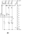
- FIG. 1 shows a first embodiment of the present invention.
- VD1 ⁇ VD2 (k ⁇ T ⁇ q) ⁇ ln (10 ⁇ I1 ⁇ I2)
- T 300 ° K.
- This is a differential amplifier composed of an N-channel transistor differential pair M6 and M7, P-channel transistor active loads M1 and M2, and a tunnel current element Ts which operates equivalently as a current source.
- both ends of the tunnel current element T0 become equal to VD1-VD2 as much as possible.
- the process so far is the same as the conventional example except for the tunnel current element Ts.
- a gate-to-back gate of a P-channel transistor is used as an example of a tunnel current element.
- the source and drain of such a transistor are connected to, for example, a back gate.
- circuit simulation can be performed using an existing transistor model such as BSIM4.
- BSIM4 transistor model
- the tunnel current elements T1 to T10 having the same shape as the tunnel current element T0 are connected in series and the currents of the P-channel transistors M4 and M5 are set equal to each other, whereby an equal current flows through the tunnel current elements T0 to T10.
- each tunnel current element The voltages at both ends of each tunnel current element are equal to each other. That is, a voltage 10 times that of the tunnel current element T0 is generated at both ends of the series connection of the tunnel current elements T1 to T10.
- This voltage is a voltage proportional to the absolute temperature at about 600 mV and having a temperature characteristic of +2 mV / ° C. at room temperature, as in the conventional example.
- This voltage is added to the forward voltage VD3 (approximately 0.7 V) generated at the junction D3 having a temperature characteristic of about ⁇ 2 mV / ° C., and is output as the reference voltage Vout.
- the reference voltage At about 1.3 V, the reference voltage has zero temperature characteristics.
- the voltage and temperature coefficient of VD3 vary somewhat depending on the process and current density. Therefore, the number and size of the tunnel current elements are adjusted accordingly, and the voltage of the desired temperature characteristic including zero is designed to obtain a voltage. .
- the current consumption is about 10 pA for each current, the entire current can be suppressed to about several tens of pA. A power consumption of about several tens to 100 pW can be realized.
- the area of the tunnel current element is reduced, the current is reduced proportionally. Therefore, for example, if the area of each tunnel current element is 10 ⁇ m ⁇ 10 ⁇ m, the power consumption can be reduced to 1/9.
- a resistor is used as in the conventional example, it is a good contrast to the fact that the area of the resistor and the current consumption are inversely proportional.
- the above-mentioned size, current value, etc. are examples for explanation, and can be changed as appropriate according to requirements and processes.
- the gate / tunnel / leakage current of transistors other than the tunnel current element is a concern, it is necessary to make these transistors with high withstand voltage transistors for input / output that have a thick gate thickness and little tunnel current flows.
- the number of tunneling current elements connected in series is not limited to the above example, and can be appropriately selected according to the area ratio of the junctions D1 and D2. It is also possible to adjust the voltage generated at both ends of the series connection of tunnel current elements T1 to T10 by adjusting the ratio of P-channel transistors M3 and M4. For example, the drive capability of the load can be increased by doubling the size of the P-channel transistor M5 and doubling the area of the tunnel current element.
- the electrode area of the tunnel current element T0 is about four times T1.
- the circuit made with the conventional resistance ratio is replaced to reduce the power consumption.
- the electrode area of T2 to T5 is the same as the area of T1
- the voltage at both ends of T1 to T5 is 10 times that of T0, so that T6 to T10 can be omitted (not shown).
- the electrode area ratio including the fraction and any number can be set, and desired characteristics can be adjusted.
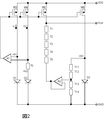
- FIG. 2 shows a second embodiment of the present invention.
- Components having the same functions as those in FIG. Due to the drain current of the P-channel transistor M5, a voltage five times the voltage generated in the tunnel current element T0 is generated at both ends of the series connection of the tunnel current elements T1 to T5. In the case of the same area ratio of the junction as in FIG. 1, this voltage is -1 mV / ° C. at 300 mV.
- a forward voltage VD3 is generated at the junction D3 by the newly added P-channel transistor M8, divided by two by the tunnel current elements T11 to T14, and a voltage half of VD3 is generated by the voltage follower circuit by the differential amplifier A2. I am letting.
- This voltage is about 350 mV and has a temperature characteristic of about ⁇ 1 mV / ° C.
- the sum of this voltage and the voltage generated at both ends of the series connection of the tunnel current elements T1 to T5 is generated at the output terminal Vout.
- the voltage is about 650 mV, and the temperature coefficient cancels out and becomes almost zero.
- the voltage division ratio can be arbitrarily selected, such as 1/3 or 2/3. In that case, a desired output voltage can be selected by appropriately selecting a ratio of the junction area ratio and the number and size of tunnel current elements connected in series. And temperature coefficient can be realized.
- the power is reduced by an order of magnitude compared to the prior art, and the power supply voltage operates with only 1 V, and a voltage half that of the bandgap reference can be obtained. If the ratio of the transistors M3, M4, M5, and M8 is 1: 1: 1: 1, the power consumption is only 40 pW.
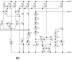
- FIG. 3 shows an embodiment in which the second embodiment of the present invention is described at the transistor level. Components having the same functions as those in FIG. Here, an example is shown in which transistors whose gate tunnel current is not negligible are used. It is known that the PNP transistors Q1, Q2 and Q3 have bases and collectors respectively connected and operate as equivalent junctions. In particular, in the CMOS process, a PNP transistor having a substrate as a collector, an N well as a base, and a diffusion layer for the source and drain of a P-channel transistor as an emitter can be made without additional cost.
- the forward voltage VD3 generated in the PNP transistor Q3 is divided into two by the tunnel current elements T11 to T14.
- T11 and T12 in the opposite directions, the back gate between them can be connected by the same N well, and the wiring connecting the lead electrode of the back gate and both can be omitted.
- the drain can also be shared.
- T13 and T14 As a result, the size can be further reduced. It is to be noted that any partial pressure can be obtained by appropriately selecting the size and number of the tunnel current elements using the formula described in the paragraph 0018.
- the differential amplifier A2 includes a differential pair composed of P-channel transistors M15 and M16, an active load composed of N-channel transistors M18 and M19, and a common source circuit composed of an N-channel transistor M17. Since the differential amplifier A2 operates as a voltage follower, the gates of the transistors M15 and M16 and the drain of the transistor M17 have substantially the same potential, and the back gates of the transistors M15 and M16 are connected thereto. For this reason, in both the transistors M15 and M16, the gate and back gate are almost 0 V, and no current flows between them. That is, the gate tunnel current of these transistors can be made zero.
- the drain current of the P-channel transistor M15 becomes the drain current of the N-channel transistor M18 and is also supplied as the gate / tunnel current of the N-channel transistors M18 and M19.
- the gate-tunnel current of the N-channel transistor M17 is set to be approximately equal to the latter.
- the gate area of the N-channel transistor M17 is made substantially equal to the sum of the N-channel transistors M18 and M19, and all these current densities are made equal.
- the gate-back gate voltages of these three transistors are equalized, the gate-back gate tunnel currents are made uniform, and the drain currents when the P-channel transistors M15 and M16 are balanced can be made to flow out equally.
- the main part of the differential amplifier A1 includes a differential pair composed of N-channel transistors M6 and M7, an active load composed of P-channel transistors M1 and M2, and a tunnel current element Ts regarded as a substantially constant current source.
- the tunnel current element Ts can be made in a substrate portion between the gate and the back gate of an N-channel transistor, and can be made smaller than that made of a P-channel transistor.
- the P channel transistor M10 operating as a constant current source and the N channel transistor M13 operating as a diode generate a voltage VGS higher than the common source voltage of the differential pair composed of the N channel transistors M6 and M7. Since this voltage is approximately equal to the gate voltages of both N-channel transistors M6 and M7, this voltage biases these common back gates. As a result, the base-back gate voltage of these transistors becomes almost 0 V, and no gate-tunnel current flows.
- a process called a deep N well is generally used, but is not limited thereto.
- a P-channel transistor M11 is inserted in order to compensate the balance deterioration due to the gate-tunnel current of the circuit composed of the P-channel transistors M1, M2 and M10.
- the source current of the P channel transistor M11 is a small value because it is only the gate tunnel current of the P channel transistors M1, M2 and M10. Therefore, the P-channel transistor M11 can be made as small as possible, and the gate / tunnel current can be suppressed.
- the P-channel transistor M12 is inserted in order to compensate for the influence of the gate / tunnel current of the current source P-channel transistors M3, M4, M5, M14 and M8 in the subsequent stage.
- the balance can be further improved by designing the current value and the gate size so that the gate and tunnel currents of the P-channel transistor M12 and the P-channel transistor M11 are approximately equal.
- the band gap preference circuit can be configured with the same size as the conventional one with 1 nA or less, which is 4 digits smaller than the conventional one.
- the operating time of a portable device powered by a battery can be dramatically increased. It is possible to use not only a battery but also a weak power source by a magnetic field, an electric field, photovoltaic power generation, a contact potential, etc., and can be applied to a device embedded in a living body without a battery.
- this invention is not limited to what was illustrated as an Example, It can also cut out a part and can implement it, combining arbitrarily.
- the reference voltage generation circuit of FIG. 2 is described at the transistor level.
- T1 to T14 Ts Tunnel current elements D1 to D3 Semiconductor junctions M1 to M19 Transistors I0 to I4 Current sources R1 to R3 Resistors A1 and A2 Differential amplifier VDD Power supply GND Ground Vout Output terminal
Landscapes
- Engineering & Computer Science (AREA)
- Physics & Mathematics (AREA)
- Microelectronics & Electronic Packaging (AREA)
- Electromagnetism (AREA)
- General Physics & Mathematics (AREA)
- Radar, Positioning & Navigation (AREA)
- Automation & Control Theory (AREA)
- Power Engineering (AREA)
- Nonlinear Science (AREA)
- Control Of Electrical Variables (AREA)
- Amplifiers (AREA)
- Semiconductor Integrated Circuits (AREA)
Priority Applications (1)
| Application Number | Priority Date | Filing Date | Title |
|---|---|---|---|
| US13/261,789 US20140197815A1 (en) | 2011-06-12 | 2012-05-21 | Tunneling current circuit |
Applications Claiming Priority (2)
| Application Number | Priority Date | Filing Date | Title |
|---|---|---|---|
| JP2011-130765 | 2011-06-12 | ||
| JP2011130765A JP5707634B2 (ja) | 2011-06-12 | 2011-06-12 | トンネル電流回路 |
Publications (1)
| Publication Number | Publication Date |
|---|---|
| WO2012172927A1 true WO2012172927A1 (ja) | 2012-12-20 |
Family
ID=47356921
Family Applications (1)
| Application Number | Title | Priority Date | Filing Date |
|---|---|---|---|
| PCT/JP2012/062894 Ceased WO2012172927A1 (ja) | 2011-06-12 | 2012-05-21 | トンネル電流回路 |
Country Status (3)
| Country | Link |
|---|---|
| US (1) | US20140197815A1 (enExample) |
| JP (1) | JP5707634B2 (enExample) |
| WO (1) | WO2012172927A1 (enExample) |
Cited By (1)
| Publication number | Priority date | Publication date | Assignee | Title |
|---|---|---|---|---|
| CN111247768A (zh) * | 2017-10-17 | 2020-06-05 | 量子加密有限公司 | 基于量子效应的唯一标识符 |
Families Citing this family (1)
| Publication number | Priority date | Publication date | Assignee | Title |
|---|---|---|---|---|
| US11349446B2 (en) * | 2020-03-10 | 2022-05-31 | SiliconIntervention Inc. | Amplifier bias control using tunneling current |
Citations (6)
| Publication number | Priority date | Publication date | Assignee | Title |
|---|---|---|---|---|
| JPH0779154A (ja) * | 1993-06-30 | 1995-03-20 | Toshiba Corp | 一電子トンネル素子を用いたインバータ |
| JP2002064150A (ja) * | 2000-06-05 | 2002-02-28 | Mitsubishi Electric Corp | 半導体装置 |
| JP2002304224A (ja) * | 2000-12-08 | 2002-10-18 | Nec Corp | 電圧発生回路および電圧発生方法 |
| US20030107431A1 (en) * | 2001-12-10 | 2003-06-12 | Tang Stephen H. | Balancing gate-leakage current in differential pair circuits |
| JP2004147175A (ja) * | 2002-10-25 | 2004-05-20 | Renesas Technology Corp | 半導体装置 |
| JP2012088978A (ja) * | 2010-10-20 | 2012-05-10 | Mitsutoshi Sugawara | 基準電圧発生回路 |
Family Cites Families (8)
| Publication number | Priority date | Publication date | Assignee | Title |
|---|---|---|---|---|
| US3588672A (en) * | 1968-02-08 | 1971-06-28 | Tektronix Inc | Current regulator controlled by voltage across semiconductor junction device |
| US5384530A (en) * | 1992-08-06 | 1995-01-24 | Massachusetts Institute Of Technology | Bootstrap voltage reference circuit utilizing an N-type negative resistance device |
| JP4194237B2 (ja) * | 1999-12-28 | 2008-12-10 | 株式会社リコー | 電界効果トランジスタを用いた電圧発生回路及び基準電圧源回路 |
| JP2004085526A (ja) * | 2001-12-05 | 2004-03-18 | Renesas Technology Corp | 半導体装置 |
| US6989659B2 (en) * | 2002-09-09 | 2006-01-24 | Acutechnology Semiconductor | Low dropout voltage regulator using a depletion pass transistor |
| JP2005204297A (ja) * | 2003-12-18 | 2005-07-28 | Matsushita Electric Ind Co Ltd | バイアス回路を搭載した増幅装置 |
| US7498869B2 (en) * | 2007-01-15 | 2009-03-03 | International Business Machines Corporation | Voltage reference circuit for low voltage applications in an integrated circuit |
| JP4726885B2 (ja) * | 2007-11-30 | 2011-07-20 | ルネサスエレクトロニクス株式会社 | 半導体回路装置 |
-
2011
- 2011-06-12 JP JP2011130765A patent/JP5707634B2/ja not_active Expired - Fee Related
-
2012
- 2012-05-21 US US13/261,789 patent/US20140197815A1/en not_active Abandoned
- 2012-05-21 WO PCT/JP2012/062894 patent/WO2012172927A1/ja not_active Ceased
Patent Citations (6)
| Publication number | Priority date | Publication date | Assignee | Title |
|---|---|---|---|---|
| JPH0779154A (ja) * | 1993-06-30 | 1995-03-20 | Toshiba Corp | 一電子トンネル素子を用いたインバータ |
| JP2002064150A (ja) * | 2000-06-05 | 2002-02-28 | Mitsubishi Electric Corp | 半導体装置 |
| JP2002304224A (ja) * | 2000-12-08 | 2002-10-18 | Nec Corp | 電圧発生回路および電圧発生方法 |
| US20030107431A1 (en) * | 2001-12-10 | 2003-06-12 | Tang Stephen H. | Balancing gate-leakage current in differential pair circuits |
| JP2004147175A (ja) * | 2002-10-25 | 2004-05-20 | Renesas Technology Corp | 半導体装置 |
| JP2012088978A (ja) * | 2010-10-20 | 2012-05-10 | Mitsutoshi Sugawara | 基準電圧発生回路 |
Cited By (2)
| Publication number | Priority date | Publication date | Assignee | Title |
|---|---|---|---|---|
| CN111247768A (zh) * | 2017-10-17 | 2020-06-05 | 量子加密有限公司 | 基于量子效应的唯一标识符 |
| CN111247768B (zh) * | 2017-10-17 | 2023-09-12 | 量子加密有限公司 | 基于量子效应的唯一标识符 |
Also Published As
| Publication number | Publication date |
|---|---|
| JP2013003615A (ja) | 2013-01-07 |
| JP5707634B2 (ja) | 2015-04-30 |
| US20140197815A1 (en) | 2014-07-17 |
Similar Documents
| Publication | Publication Date | Title |
|---|---|---|
| US10198022B1 (en) | Ultra-low power bias current generation and utilization in current and voltage source and regulator devices | |
| CN103529897B (zh) | 一种高电源抑制比的纯mos结构电压基准源 | |
| JP6204772B2 (ja) | カスコード増幅器 | |
| JP2008108009A (ja) | 基準電圧発生回路 | |
| KR101451468B1 (ko) | 정전류 회로 및 기준 전압 회로 | |
| CN108351662A (zh) | 具有曲率补偿的带隙参考电路 | |
| CN110895423B (zh) | 用于与绝对温度成比例电路的系统和方法 | |
| CN103353782A (zh) | 低供电电压带隙参考电路及方法 | |
| JP2014515506A (ja) | 調整可能な温度感受性を有する低電力な基準電流生成器 | |
| CN109491433B (zh) | 一种适用于图像传感器的基准电压源电路结构 | |
| JP5640636B2 (ja) | 基準電圧発生回路 | |
| JP3195770B2 (ja) | 基準電圧発生回路 | |
| JP5707634B2 (ja) | トンネル電流回路 | |
| CN104977968B (zh) | 一种高阶温度补偿的带隙基准电路 | |
| US10310539B2 (en) | Proportional to absolute temperature reference circuit and a voltage reference circuit | |
| TWI716323B (zh) | 電壓產生器 | |
| CN107422777A (zh) | Ptat电流源 | |
| TW200848975A (en) | Current generator | |
| CN104345765A (zh) | 能带隙参考电压产生电路与使用其的电子系统 | |
| JP5262718B2 (ja) | バイアス回路 | |
| TWI564692B (zh) | 能隙參考電路 | |
| JP5175131B2 (ja) | 半導体集積回路装置 | |
| US20150015326A1 (en) | Bulk-modulated current source | |
| US20150061747A1 (en) | Proportional-to-supply analog current generator | |
| CN106292831B (zh) | 可调式镜射比率的电流镜 |
Legal Events
| Date | Code | Title | Description |
|---|---|---|---|
| 121 | Ep: the epo has been informed by wipo that ep was designated in this application |
Ref document number: 12800674 Country of ref document: EP Kind code of ref document: A1 |
|
| WWE | Wipo information: entry into national phase |
Ref document number: 13261789 Country of ref document: US |
|
| NENP | Non-entry into the national phase |
Ref country code: DE |
|
| 122 | Ep: pct application non-entry in european phase |
Ref document number: 12800674 Country of ref document: EP Kind code of ref document: A1 |