WO2012157426A1 - 配線板及びその製造方法 - Google Patents
配線板及びその製造方法 Download PDFInfo
- Publication number
- WO2012157426A1 WO2012157426A1 PCT/JP2012/061143 JP2012061143W WO2012157426A1 WO 2012157426 A1 WO2012157426 A1 WO 2012157426A1 JP 2012061143 W JP2012061143 W JP 2012061143W WO 2012157426 A1 WO2012157426 A1 WO 2012157426A1
- Authority
- WO
- WIPO (PCT)
- Prior art keywords
- wiring board
- substrate
- conductor
- protrusion
- electronic devices
- Prior art date
- Legal status (The legal status is an assumption and is not a legal conclusion. Google has not performed a legal analysis and makes no representation as to the accuracy of the status listed.)
- Ceased
Links
Images




















Classifications
-
- H—ELECTRICITY
- H05—ELECTRIC TECHNIQUES NOT OTHERWISE PROVIDED FOR
- H05K—PRINTED CIRCUITS; CASINGS OR CONSTRUCTIONAL DETAILS OF ELECTRIC APPARATUS; MANUFACTURE OF ASSEMBLAGES OF ELECTRICAL COMPONENTS
- H05K1/00—Printed circuits
- H05K1/18—Printed circuits structurally associated with non-printed electric components
- H05K1/182—Printed circuits structurally associated with non-printed electric components associated with components mounted in printed circuit boards [PCB], e.g. insert-mounted components [IMC]
- H05K1/185—Printed circuits structurally associated with non-printed electric components associated with components mounted in printed circuit boards [PCB], e.g. insert-mounted components [IMC] associated with components encapsulated in the insulating substrate of the PCBs; associated with components incorporated in internal layers of multilayer circuit boards
-
- H—ELECTRICITY
- H05—ELECTRIC TECHNIQUES NOT OTHERWISE PROVIDED FOR
- H05K—PRINTED CIRCUITS; CASINGS OR CONSTRUCTIONAL DETAILS OF ELECTRIC APPARATUS; MANUFACTURE OF ASSEMBLAGES OF ELECTRICAL COMPONENTS
- H05K3/00—Apparatus or processes for manufacturing printed circuits
- H05K3/46—Manufacturing multilayer circuits
-
- H—ELECTRICITY
- H05—ELECTRIC TECHNIQUES NOT OTHERWISE PROVIDED FOR
- H05K—PRINTED CIRCUITS; CASINGS OR CONSTRUCTIONAL DETAILS OF ELECTRIC APPARATUS; MANUFACTURE OF ASSEMBLAGES OF ELECTRICAL COMPONENTS
- H05K3/00—Apparatus or processes for manufacturing printed circuits
- H05K3/30—Assembling printed circuits with electric components, e.g. with resistors
- H05K3/306—Assembling printed circuits with electric components, e.g. with resistors with lead-in-hole components
-
- H—ELECTRICITY
- H10—SEMICONDUCTOR DEVICES; ELECTRIC SOLID-STATE DEVICES NOT OTHERWISE PROVIDED FOR
- H10W—GENERIC PACKAGES, INTERCONNECTIONS, CONNECTORS OR OTHER CONSTRUCTIONAL DETAILS OF DEVICES COVERED BY CLASS H10
- H10W70/00—Package substrates; Interposers; Redistribution layers [RDL]
- H10W70/01—Manufacture or treatment
- H10W70/05—Manufacture or treatment of insulating or insulated package substrates, or of interposers, or of redistribution layers
- H10W70/08—Manufacture or treatment of insulating or insulated package substrates, or of interposers, or of redistribution layers by depositing layers on the chip or wafer, e.g. "chip-first" RDLs
- H10W70/09—Manufacture or treatment of insulating or insulated package substrates, or of interposers, or of redistribution layers by depositing layers on the chip or wafer, e.g. "chip-first" RDLs extending onto an encapsulation that laterally surrounds the chip or wafer, e.g. fan-out wafer level package [FOWLP] RDLs
-
- H—ELECTRICITY
- H10—SEMICONDUCTOR DEVICES; ELECTRIC SOLID-STATE DEVICES NOT OTHERWISE PROVIDED FOR
- H10W—GENERIC PACKAGES, INTERCONNECTIONS, CONNECTORS OR OTHER CONSTRUCTIONAL DETAILS OF DEVICES COVERED BY CLASS H10
- H10W70/00—Package substrates; Interposers; Redistribution layers [RDL]
- H10W70/60—Insulating or insulated package substrates; Interposers; Redistribution layers
- H10W70/67—Insulating or insulated package substrates; Interposers; Redistribution layers characterised by their insulating layers or insulating parts
- H10W70/68—Shapes or dispositions thereof
- H10W70/685—Shapes or dispositions thereof comprising multiple insulating layers
-
- H—ELECTRICITY
- H10—SEMICONDUCTOR DEVICES; ELECTRIC SOLID-STATE DEVICES NOT OTHERWISE PROVIDED FOR
- H10W—GENERIC PACKAGES, INTERCONNECTIONS, CONNECTORS OR OTHER CONSTRUCTIONAL DETAILS OF DEVICES COVERED BY CLASS H10
- H10W72/00—Interconnections or connectors in packages
-
- H—ELECTRICITY
- H05—ELECTRIC TECHNIQUES NOT OTHERWISE PROVIDED FOR
- H05K—PRINTED CIRCUITS; CASINGS OR CONSTRUCTIONAL DETAILS OF ELECTRIC APPARATUS; MANUFACTURE OF ASSEMBLAGES OF ELECTRICAL COMPONENTS
- H05K2201/00—Indexing scheme relating to printed circuits covered by H05K1/00
- H05K2201/10—Details of components or other objects attached to or integrated in a printed circuit board
- H05K2201/10007—Types of components
- H05K2201/10015—Non-printed capacitor
-
- H—ELECTRICITY
- H05—ELECTRIC TECHNIQUES NOT OTHERWISE PROVIDED FOR
- H05K—PRINTED CIRCUITS; CASINGS OR CONSTRUCTIONAL DETAILS OF ELECTRIC APPARATUS; MANUFACTURE OF ASSEMBLAGES OF ELECTRICAL COMPONENTS
- H05K2201/00—Indexing scheme relating to printed circuits covered by H05K1/00
- H05K2201/10—Details of components or other objects attached to or integrated in a printed circuit board
- H05K2201/10007—Types of components
- H05K2201/1003—Non-printed inductor
-
- H—ELECTRICITY
- H05—ELECTRIC TECHNIQUES NOT OTHERWISE PROVIDED FOR
- H05K—PRINTED CIRCUITS; CASINGS OR CONSTRUCTIONAL DETAILS OF ELECTRIC APPARATUS; MANUFACTURE OF ASSEMBLAGES OF ELECTRICAL COMPONENTS
- H05K2201/00—Indexing scheme relating to printed circuits covered by H05K1/00
- H05K2201/10—Details of components or other objects attached to or integrated in a printed circuit board
- H05K2201/10613—Details of electrical connections of non-printed components, e.g. special leads
- H05K2201/10621—Components characterised by their electrical contacts
- H05K2201/10636—Leadless chip, e.g. chip capacitor or resistor
-
- H—ELECTRICITY
- H05—ELECTRIC TECHNIQUES NOT OTHERWISE PROVIDED FOR
- H05K—PRINTED CIRCUITS; CASINGS OR CONSTRUCTIONAL DETAILS OF ELECTRIC APPARATUS; MANUFACTURE OF ASSEMBLAGES OF ELECTRICAL COMPONENTS
- H05K2203/00—Indexing scheme relating to apparatus or processes for manufacturing printed circuits covered by H05K3/00
- H05K2203/14—Related to the order of processing steps
- H05K2203/1461—Applying or finishing the circuit pattern after another process, e.g. after filling of vias with conductive paste, after making printed resistors
- H05K2203/1469—Circuit made after mounting or encapsulation of the components
-
- H—ELECTRICITY
- H05—ELECTRIC TECHNIQUES NOT OTHERWISE PROVIDED FOR
- H05K—PRINTED CIRCUITS; CASINGS OR CONSTRUCTIONAL DETAILS OF ELECTRIC APPARATUS; MANUFACTURE OF ASSEMBLAGES OF ELECTRICAL COMPONENTS
- H05K3/00—Apparatus or processes for manufacturing printed circuits
- H05K3/46—Manufacturing multilayer circuits
- H05K3/4602—Manufacturing multilayer circuits characterized by a special circuit board as base or central core whereon additional circuit layers are built or additional circuit boards are laminated
-
- H—ELECTRICITY
- H10—SEMICONDUCTOR DEVICES; ELECTRIC SOLID-STATE DEVICES NOT OTHERWISE PROVIDED FOR
- H10W—GENERIC PACKAGES, INTERCONNECTIONS, CONNECTORS OR OTHER CONSTRUCTIONAL DETAILS OF DEVICES COVERED BY CLASS H10
- H10W70/00—Package substrates; Interposers; Redistribution layers [RDL]
- H10W70/60—Insulating or insulated package substrates; Interposers; Redistribution layers
-
- H—ELECTRICITY
- H10—SEMICONDUCTOR DEVICES; ELECTRIC SOLID-STATE DEVICES NOT OTHERWISE PROVIDED FOR
- H10W—GENERIC PACKAGES, INTERCONNECTIONS, CONNECTORS OR OTHER CONSTRUCTIONAL DETAILS OF DEVICES COVERED BY CLASS H10
- H10W70/00—Package substrates; Interposers; Redistribution layers [RDL]
- H10W70/60—Insulating or insulated package substrates; Interposers; Redistribution layers
- H10W70/67—Insulating or insulated package substrates; Interposers; Redistribution layers characterised by their insulating layers or insulating parts
- H10W70/68—Shapes or dispositions thereof
- H10W70/682—Shapes or dispositions thereof comprising holes having chips therein
-
- H—ELECTRICITY
- H10—SEMICONDUCTOR DEVICES; ELECTRIC SOLID-STATE DEVICES NOT OTHERWISE PROVIDED FOR
- H10W—GENERIC PACKAGES, INTERCONNECTIONS, CONNECTORS OR OTHER CONSTRUCTIONAL DETAILS OF DEVICES COVERED BY CLASS H10
- H10W72/00—Interconnections or connectors in packages
- H10W72/851—Dispositions of multiple connectors or interconnections
- H10W72/874—On different surfaces
-
- H—ELECTRICITY
- H10—SEMICONDUCTOR DEVICES; ELECTRIC SOLID-STATE DEVICES NOT OTHERWISE PROVIDED FOR
- H10W—GENERIC PACKAGES, INTERCONNECTIONS, CONNECTORS OR OTHER CONSTRUCTIONAL DETAILS OF DEVICES COVERED BY CLASS H10
- H10W72/00—Interconnections or connectors in packages
- H10W72/90—Bond pads, in general
- H10W72/941—Dispositions of bond pads
- H10W72/9413—Dispositions of bond pads on encapsulations
-
- H—ELECTRICITY
- H10—SEMICONDUCTOR DEVICES; ELECTRIC SOLID-STATE DEVICES NOT OTHERWISE PROVIDED FOR
- H10W—GENERIC PACKAGES, INTERCONNECTIONS, CONNECTORS OR OTHER CONSTRUCTIONAL DETAILS OF DEVICES COVERED BY CLASS H10
- H10W90/00—Package configurations
- H10W90/701—Package configurations characterised by the relative positions of pads or connectors relative to package parts
- H10W90/731—Package configurations characterised by the relative positions of pads or connectors relative to package parts of die-attach connectors
- H10W90/734—Package configurations characterised by the relative positions of pads or connectors relative to package parts of die-attach connectors between a chip and a stacked insulating package substrate, interposer or RDL
-
- Y—GENERAL TAGGING OF NEW TECHNOLOGICAL DEVELOPMENTS; GENERAL TAGGING OF CROSS-SECTIONAL TECHNOLOGIES SPANNING OVER SEVERAL SECTIONS OF THE IPC; TECHNICAL SUBJECTS COVERED BY FORMER USPC CROSS-REFERENCE ART COLLECTIONS [XRACs] AND DIGESTS
- Y02—TECHNOLOGIES OR APPLICATIONS FOR MITIGATION OR ADAPTATION AGAINST CLIMATE CHANGE
- Y02P—CLIMATE CHANGE MITIGATION TECHNOLOGIES IN THE PRODUCTION OR PROCESSING OF GOODS
- Y02P70/00—Climate change mitigation technologies in the production process for final industrial or consumer products
- Y02P70/50—Manufacturing or production processes characterised by the final manufactured product
-
- Y—GENERAL TAGGING OF NEW TECHNOLOGICAL DEVELOPMENTS; GENERAL TAGGING OF CROSS-SECTIONAL TECHNOLOGIES SPANNING OVER SEVERAL SECTIONS OF THE IPC; TECHNICAL SUBJECTS COVERED BY FORMER USPC CROSS-REFERENCE ART COLLECTIONS [XRACs] AND DIGESTS
- Y10—TECHNICAL SUBJECTS COVERED BY FORMER USPC
- Y10T—TECHNICAL SUBJECTS COVERED BY FORMER US CLASSIFICATION
- Y10T29/00—Metal working
- Y10T29/49—Method of mechanical manufacture
- Y10T29/49002—Electrical device making
- Y10T29/49117—Conductor or circuit manufacturing
- Y10T29/49124—On flat or curved insulated base, e.g., printed circuit, etc.
-
- Y—GENERAL TAGGING OF NEW TECHNOLOGICAL DEVELOPMENTS; GENERAL TAGGING OF CROSS-SECTIONAL TECHNOLOGIES SPANNING OVER SEVERAL SECTIONS OF THE IPC; TECHNICAL SUBJECTS COVERED BY FORMER USPC CROSS-REFERENCE ART COLLECTIONS [XRACs] AND DIGESTS
- Y10—TECHNICAL SUBJECTS COVERED BY FORMER USPC
- Y10T—TECHNICAL SUBJECTS COVERED BY FORMER US CLASSIFICATION
- Y10T29/00—Metal working
- Y10T29/49—Method of mechanical manufacture
- Y10T29/49002—Electrical device making
- Y10T29/49117—Conductor or circuit manufacturing
- Y10T29/49124—On flat or curved insulated base, e.g., printed circuit, etc.
- Y10T29/4913—Assembling to base an electrical component, e.g., capacitor, etc.
- Y10T29/49139—Assembling to base an electrical component, e.g., capacitor, etc. by inserting component lead or terminal into base aperture
Definitions
- the present invention relates to a wiring board and a manufacturing method thereof.
- Patent Document 1 discloses a substrate having an opening, a plurality of electronic components accommodated in the opening, an insulating layer formed on the substrate and the electronic component, and a conductor formed on the insulating layer.
- a wiring board having a layer, a via conductor that electrically connects the conductor layer and the electrode of the electronic component to each other is disclosed.
- the electronic components when a plurality of electronic components are accommodated in one opening, the electronic components are likely to be misaligned. Specifically, the electronic components may be misaligned during mounting or due to the fluidity of the filled resin after mounting. And when the position shift of an electronic component arises, it will become easy to produce the connection failure of an electronic component and a via conductor. In particular, when the electronic component has side electrodes, a short circuit between adjacent electrodes may be a concern.
- the present invention has been made in view of such circumstances, and an object of the present invention is to suppress displacement of an electronic device when a plurality of electronic devices are accommodated in one opening. Another object of the present invention is to improve the reliability of electrical connection of an electronic device incorporated in a wiring board.
- a wiring board according to the present invention includes a substrate having an opening, a plurality of electronic devices disposed in the one opening, an insulating layer disposed on the substrate and the electronic device, and the insulating layer.
- a protrusion formed on the wall surface of the opening, and the tip of the protrusion is inserted between the adjacent electronic devices in at least one place.
- the method of manufacturing a wiring board according to the present invention includes preparing a substrate, forming an opening having a protrusion on a wall surface of the substrate, and forming the protrusion between adjacent electronic devices at least at one place. Arranging a plurality of electronic devices in one of the openings so that the front end enters, forming an insulating layer on the substrate and the electronic device, and forming a conductor layer on the insulating layer And including.
- the present invention for example, when a plurality of electronic devices are accommodated in one opening, it is possible to suppress displacement of the electronic devices. Further, according to the present invention, in addition to this effect or instead of this effect, there is a case where the effect of improving the reliability of the electrical connection of the electronic device incorporated in the wiring board may be achieved.
- FIG. 3 is a sectional view taken along line BB in FIG. It is a figure which expands and shows between adjacent electronic components. It is a figure which shows the example in which the adjacent electronic component was arrange
- FIG. 9 is a diagram for explaining a first step of forming a core part in the manufacturing method shown in FIG. 8.
- FIG. 9 is a diagram for explaining a second step of forming a core part in the manufacturing method shown in FIG. 8.
- FIG. 9 is a diagram for explaining a third step of forming a core part in the manufacturing method shown in FIG. 8.
- FIG. 10 is a diagram for explaining a fourth step of forming the core portion in the manufacturing method shown in FIG. 8.
- FIG. 9 is a diagram for explaining a step of forming a cavity in the manufacturing method shown in FIG. 8.
- FIG. 9 is a diagram for explaining a first method for forming a cavity in the manufacturing method shown in FIG. 8. It is a figure for demonstrating the 2nd method for forming a cavity in the manufacturing method shown in FIG.
- FIG. 9 is a diagram for explaining a third method for forming a cavity in the manufacturing method shown in FIG. 8.
- FIG. 9 is a diagram showing a core substrate after forming a cavity in the manufacturing method shown in FIG. 8.
- FIG. 9 is a diagram for explaining a process of attaching a core substrate on which a cavity is formed to a carrier in the manufacturing method shown in FIG. 8.
- FIG. 9 is a diagram for explaining a process of attaching a core substrate on which a cavity is formed to a carrier in the manufacturing method shown in FIG. 8.
- FIG. 9 is a diagram for explaining a step of arranging a plurality of electronic components in the cavity in the manufacturing method shown in FIG. 8.
- FIG. 9 is a diagram illustrating a state in which a plurality of electronic components are arranged in a cavity in the manufacturing method illustrated in FIG. 8.
- FIG. 9 is a diagram for explaining a step of forming a first interlayer insulating layer and a first copper foil on an insulating substrate and an electronic component in the manufacturing method shown in FIG. 8.
- it is a figure for demonstrating a press process. It is a figure which shows the state after the press of FIG. FIG.
- FIG. 9 is a diagram for explaining a step of forming a second interlayer insulating layer and a second copper foil on the insulating substrate and the electronic component after removing the carrier in the manufacturing method shown in FIG. 8.
- a first step for forming a conductor layer on the first and second interlayer insulating layers and electrically connecting each conductor layer and the electrode of the electronic component will be described.
- FIG. It is a figure for demonstrating the 2nd process after the process of FIG. It is a figure for demonstrating the 3rd process after the process of FIG. It is a figure for demonstrating the process of mounting an electronic component on the surface of the wiring board which concerns on embodiment of this invention.
- it is a top view which shows the wiring board in which three electronic devices are incorporated. In other embodiment of this invention, it is a top view which shows the wiring board in which four electronic devices are incorporated. In other embodiment of this invention, it is a top view which shows the wiring board in which each of four electronic devices is enclosed by the cut surface of a board
- FIG. 43B is a diagram for explaining a second step after the step of FIG. 43A.
- arrows Z1 and Z2 indicate the stacking direction of the wiring boards (or the thickness direction of the wiring boards) corresponding to the normal direction of the main surface (front and back surfaces) of the wiring boards.
- arrows X1 and X2 and Y1 and Y2 respectively indicate directions orthogonal to the stacking direction (or sides of each layer).
- the main surface of the wiring board is an XY plane.
- the side surface of the wiring board is an XZ plane or a YZ plane.
- the two principal surfaces facing the opposite normal directions are referred to as the first surface or the third surface (Z1 side surface), the second surface or the fourth surface (Z2 side surface).
- the side closer to the core is referred to as the lower layer (or inner layer side)
- the side far from the core is referred to as the upper layer (or outer layer side).
- the Z direction Z1 side or Z2 side
- the planar shape means the shape of the XY plane unless otherwise specified.
- the conductor layer is a layer composed of one or more conductor patterns.
- the conductor layer may include a conductor pattern that constitutes an electric circuit, for example, a wiring (including a ground), a pad, a land, or the like, or a planar conductor pattern that does not constitute an electric circuit.
- the opening includes notches and cuts in addition to holes and grooves.
- the hole is not limited to a through hole, and includes a non-through hole.
- the holes include via holes and through holes.
- a conductor formed in the via hole (wall surface or bottom surface)
- a conductor formed in the through hole (wall surface) is referred to as a through hole conductor.
- plating includes dry plating such as PVD (Physical Vapor Deposition) and CVD (Chemical Vapor Deposition).
- Enclose includes not only completely closing one area with an unbroken ring, but also surrounding one area with a ring having some breaks.
- a ring is a plane figure formed by connecting both ends of a line, and not only a circle but also a polygon is included in the ring.
- Preparing includes purchasing and using finished products in addition to purchasing materials and parts and manufacturing them themselves.
- the electronic device is disposed in the opening includes not only that the entire electronic device is completely accommodated in the opening, but also that only a part of the electronic device is disposed in the opening.
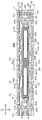
- the wiring board 10 includes a substrate 100 (insulating substrate), insulating layers 101 and 102 (interlayer insulating layers), conductor layers 110 and 120, and electronic components 200a and 200b ( Electronic device) and solder resists 11 and 12.
- the wiring board 10 of this embodiment is a rigid wiring board.
- the wiring board 10 may be a flexible wiring board.
- one of the front and back surfaces (two main surfaces) of the substrate 100 is referred to as a first surface F1, and the other is referred to as a second surface F2.
- a surface facing the same direction as the first surface F1 is referred to as a third surface F3, and the other is referred to as a fourth surface F4.
- the substrate 100 has an insulating property and becomes a core substrate of the wiring board 10.
- Through hole 300a is formed in substrate 100 (core substrate), and through hole conductor 300b is formed by filling conductor (for example, copper plating) in through hole 300a.
- the shape of the through-hole conductor 300b is, for example, an hourglass shape (a drum shape). That is, the through-hole conductor 300b has a constricted portion 300c, and the width of the through-hole conductor 300b gradually decreases from the first surface F1 toward the constricted portion 300c, and approaches the constricted portion 300c from the second surface F2. It gradually becomes smaller as it goes.
- the shape is not limited to this, and the shape of the through-hole conductor 300b is arbitrary, and may be, for example, a substantially cylindrical shape.
- the conductor layer 301 is formed on the first surface F1 of the substrate 100, and the conductor layer 302 is formed on the second surface F2 of the substrate 100.
- Each of the conductor layers 301 and 302 includes a land of the through-hole conductor 300b.
- the conductor layer 301 and the conductor layer 302 are electrically connected to each other through the through-hole conductor 300b.
- the substrate 100 has an opening that penetrates the substrate 100.
- the substrate 100 is formed with a cavity R10 as an opening, and the electronic components 200a and 200b are accommodated in the cavity R10.
- the cavity R ⁇ b> 10 includes a hole that penetrates the substrate 100.
- Each of the electronic components 200a and 200b is disposed in the cavity R10, thereby being positioned on the side of the substrate 100 (X direction or Y direction). That is, in this embodiment, a plurality of electronic devices (electronic components 200a and 200b) are arranged in one opening (cavity R10).
- substantially the entirety of each of the electronic components 200a and 200b is completely accommodated in the cavity R10.
- the present invention is not limited to this, and only a part of the electronic components 200a and 200b may be disposed in the cavity R10.
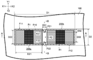
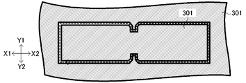
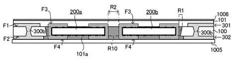
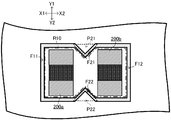
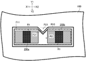
- FIG. 2 shows a state in which the electronic components 200a and 200b are accommodated in the cavity R10 of the substrate 100 (core substrate). 1 corresponds to the AA sectional view of FIG. 2, and FIG. 3 corresponds to the BB sectional view of FIG.
- the opening shapes at both ends (the first surface F1 side and the second surface F2 side) of the cavity R10 are substantially rectangular, but project on the wall surface of the cavity R10 (opening).
- the (projections P21 and P22) By forming the (projections P21 and P22), a part is constricted.
- the wall surface of the cavity R10 includes wall surfaces F11 and F12 of non-projecting portions, a distal end surface F21 of the projecting portion P21, and a distal end surface F22 of the projecting portion P22.
- the projecting part P21 and the projecting part P22 are formed on opposing wall surfaces at a position that substantially bisects the cavity R10, and the tip ends face each other to make a pair.
- the width of the cavity R10 is narrowed by the protrusions P21 and P22, and the space of the cavity R10 is divided into a space for accommodating the electronic component 200a and a space for accommodating the electronic component 200b.
- the protrusions P21 and P22 are formed on opposing wall surfaces at positions that divide the cavity R10 (opening) substantially equally (eg, approximately bisected).
- An electronic device (electronic component 200a or 200b) is accommodated in each of the spaces partitioned by the protrusions P21 and P22.
- each of the electronic components 200a and 200b is surrounded by the wall surface of the cavity R10 (the cut surface of the substrate 100).
- the electronic component 200a is surrounded by the wall surface F11 of the non-projection part, the tip surface F21 of the projection part P21, and the tip surface F22 of the projection part P22.
- the electronic component 200b is surrounded by the wall surface F12 of the non-projection part, the tip surface F21 of the projection part P21, and the tip surface F22 of the projection part P22.
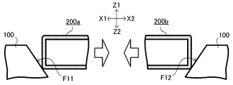
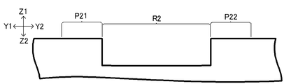
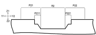
- the tip P201 of the projection P21 and the tip P202 of the projection P22 enter between the adjacent electronic components 200a and 200b (region R2 indicated by a one-dot chain line in FIG. 4A). It is out. Accordingly, when a force that brings the electronic components 200a and 200b closer to each other is applied, the movement of the electronic components 200a and 200b in the approaching direction is regulated by the protrusions P21 and P22. For this reason, it becomes difficult to contact the electronic component 200a and the electronic component 200b. As a result, a short circuit (conduction) between the electronic components 200a and 200b having side electrodes is suppressed. As shown in FIG.
- the planar shapes of the protrusions P21 and P22 are each a trumpet shape.
- Each of the protrusions P21 and P22 has a skirt that decreases in width toward the tip, and a degree that the width decreases toward the tip, and a rectangular tip.
- the protrusions P21 and P22 having such a shape are excellent in terms of laser workability, component mountability, and strength.
- the shape is not limited to this, and the shapes of the protrusions P21 and P22 are arbitrary (for example, see FIGS. 25 to 30 described later).
- the front end surface F21 of the protrusion P21 and the front end surface F22 of the protrusion P22 are each formed by a cut surface of the substrate 100.
- the front end surfaces F21 and F22 are formed by a laser cut surface.
- the present invention is not limited thereto, and for example, the front end surfaces F21 and F22 may be formed by a cut surface using a mold.
- the protrusions P21 and P22 may be provided separately from the substrate 100 (see, for example, FIG. 37 described later).
- the wall surfaces of the cavity R10 are tapered surfaces.
- the angles ⁇ 11 and ⁇ 12 between the first surface F1 of the substrate 100 and the wall surface (tapered surface) of the cavity R10 are obtuse angles. For this reason, the wall surface of cavity R10 protrudes inside cavity R10, so that it goes to the 2nd surface F2 side (Z2 side).
- all the wall surfaces (cut surfaces of the substrate 100) of the cavity R10 surrounding each of the electronic components 200a and 200b are tapered surfaces.
- the movement is restricted by the projections P21 and P22, and the tip surface F21 of the projection P21 or the tip surface of the projection P22. Due to the slope of F22, a force is exerted on the electronic components 200a and 200b in a direction to separate them. Further, even if the electronic components 200a and 200b try to go out of the cavity R10, as shown in FIG.
- the movement is restricted by the wall surfaces F11 and F12 of the non-projecting portions, and the wall surfaces F11 and F12 of the non-projecting portions. Due to the slope, a force toward the inside of the cavity R10 is applied to the electronic components 200a and 200b. As a result, the electronic components 200a and 200b are less likely to be displaced.
- the opening area at one end (Z1 side) of the cavity R10 is larger than the opening area at the other end (Z2 side). For this reason, it is easy to put the electronic components 200a and 200b into the cavity R10 from the first surface F1 side (Z1 side) of the substrate 100.
- the protrusion P21 has an edge P211 close to the cavity R10 (region R2) as shown in FIG. Further, the protrusion P22 has an edge P221 in the vicinity of the cavity R10 (region R2).
- the edges P211 and P221 are each tapered.
- the present invention is not limited to this, and the edges P211 and P221 may not be tapered in the protrusions P21 and P22 (see, for example, FIG. 31A described later).
- the width D1 in the longitudinal direction (X direction) of the cavity R10 is about 2160 ⁇ m, and the width D2 in the short direction (Y direction) of the cavity R10 is about 580 ⁇ m.
- the clearance between the electronic component 200a or 200b and the cavity R10 is about 80 ⁇ m.
- the distance between the electronic component 200a and the electronic component 200b (the width of the region R2) is in the range of about 80 to 100 ⁇ m.
- the width D31 of the protrusion P21 is preferably in the range of about 80 to 100 ⁇ m. In a particularly preferable example, the width D31 of the protrusion P21 is about 80 ⁇ m, the width D311 of the skirt is about 30 ⁇ m, and the width D312 of the tip is about 20 ⁇ m.
- the protrusion amount D32 of the protrusion P21 is about 125 ⁇ m.
- the length D321 of the skirt portion is about 40 ⁇ m, and the length D322 of the tip portion is about 85 ⁇ m.
- the width D34 of the edge P212 is about 25 ⁇ m.
- Each dimension in the projection part P22 is the same as that of the projection part P21, for example. However, the present invention is not limited to this, and the protrusion P21 and the protrusion P22 may have different dimensions.
- the angle ⁇ 11 between the first surface F1 of the substrate 100 and the tip surface F21 of the protrusion P21 is about 125 °. Further, the angle ⁇ 12 between the first surface F1 of the substrate 100 and the front end surface F22 of the protrusion P22 is about 125 °.
- the width D33 of the gap between the tip P201 of the projection P21 and the tip P202 of the projection P22 is about 330 ⁇ m.
- the width D33 is preferably narrower than the width D22 in the short direction (Y direction) of the electronic component 200a or 200b. If it is such a dimension, since the projection parts P21 and P22 located between both will prevent the electronic component 200a and the electronic component 200b from approaching each other, it will become difficult for the electronic component 200a and the electronic component 200b to contact.
- the insulator 101a is filled between the electronic components 200a and 200b and the substrate 100 (region R1) and between the electronic component 200a and the electronic component 200b (region R2) in the cavity R10. .
- the insulator 101a is made of an insulating material (more specifically, a resin) that constitutes the upper insulating layer 101 (more specifically, a resin insulation layer) (see FIG. 17 described later in more detail).
- the insulator 101a has a larger thermal expansion coefficient than both the substrate 100 and the electronic components 200a and 200b.
- the insulator 101a completely covers the periphery of the electronic components 200a and 200b. As a result, the electronic components 200a and 200b are protected by the insulator 101a (resin) and fixed at a predetermined position.
- the insulating layer 101 is formed on the first surface F1 of the substrate 100 and on the third surface F3 of the electronic components 200a and 200b.
- the insulating layer 102 is formed on the second surface F2 of the substrate 100 and on the fourth surface F4 of the electronic components 200a and 200b.
- the insulating layer 101 closes an opening on one side (first surface F1 side) of the cavity R10 (hole), and the insulating layer 102 closes an opening on the other side (second surface F2 side) of the cavity R10 (hole).
- the conductor layer 110 is formed on the insulating layer 101, and the conductor layer 120 is formed on the insulating layer 102.
- the conductor layers 110 and 120 are the outermost layers.
- the present invention is not limited to this, and more interlayer insulating layers and conductor layers may be stacked.
- the conductor layer 110 is the outermost conductor layer on the first surface F1 side
- the conductor layer 120 is the outermost conductor layer on the second surface F2 side.
- Solder resists 11 and 12 are formed on the conductor layers 110 and 120, respectively.
- openings 11a and 12a are formed in the solder resists 11 and 12, respectively.
- the predetermined part (part located in the opening part 11a) of the conductor layer 110 is exposed without being covered with the solder resist 11, and becomes the pad P11.
- part (site located in the opening part 12a) of the conductor layer 120 becomes the pad P12.
- the pad P11 becomes an external connection terminal for electrical connection with, for example, another wiring board
- the pad P12 becomes an external connection terminal for mounting an electronic component, for example.
- the application of the pads P11 and P12 is not limited to this and is arbitrary.
- the pads P11 and P12 have a corrosion-resistant layer made of, for example, a Ni / Au film on the surface thereof.
- the corrosion resistant layer can be formed by electrolytic plating or sputtering.
- the corrosion resistant layer is not an essential component and may be omitted if not necessary.
- the pads P11 and P12 are located immediately above the electronic component 200a or 200b (electronic device).
- the electrodes of the electronic devices and the electrodes just above them are arranged by via conductors (for example, via conductors 321b and 322b). It is easy to electrically connect the external connection terminal with high reliability.
- the insulating layer 101 has holes 313a (via holes), and the insulating layer 102 has holes 321a, 322a, and 323a (via holes).
- the conductors in the holes become via conductors 313b, 321b, 322b, and 323b (filled conductors), respectively.
- the via conductors 321b and 322b are electrically connected to the electrodes 210 and 220 of the electronic component 200a or 200b from the second surface F2 side of the substrate 100, respectively.
- the electronic components 200a and 200b are connected to the via conductor from one side.
- this structure is referred to as a single-sided via structure.
- the electrodes 210 and 220 of the electronic component 200a or 200b and the conductor layer 120 on the insulating layer 102 are electrically connected to each other via the via conductor 321b or 322b.
- Such a structure is advantageous for miniaturization because an electrical connection is formed in the inner layer.
- the holes 313a and 323a reach the through-hole conductor 300b, and the via conductors 313b and 323b are electrically connected to the through-hole conductor 300b from the first surface F1 side or the second surface F2 side of the substrate 100.
- the via conductors 313b and 323b are respectively disposed immediately above the through-hole conductor 300b.
- the conductor layer 301 on the first surface F1 of the substrate 100 and the conductor layer 110 on the insulating layer 101 are electrically connected to each other via the via conductor 313b, and on the second surface F2 of the substrate 100.
- the conductor layer 302 and the conductor layer 120 on the insulating layer 102 are electrically connected to each other through the via conductor 323b.
- the via conductors 313b and 323b and the through-hole conductor 300b are all filled conductors, and these are stacked in the Z direction. Such a stack structure is advantageous for miniaturization.
- the electronic components 200a and 200b are each composed of a chip capacitor.
- each of the electronic components 200a and 200b is a chip-type MLCC (multilayer ceramic capacitor) as shown in FIG. 6, for example, and includes a capacitor body 201 and an electrode 210 having a U-shaped XZ cross section. And 220.
- the capacitor body 201 includes a plurality of dielectric layers 231 to 239 and a plurality of conductor layers 211 to 214 and 221 to 224 that are alternately stacked.
- Each of the dielectric layers 231 to 239 is made of, for example, ceramic.
- the electrodes 210 and 220 are formed at both ends of the capacitor body 201, respectively.
- the capacitor body 201 is covered with electrodes 210 and 220 from the lower surface (the surface on the fourth surface F4 side), the side surface, and the upper surface (the surface on the third surface F3 side).
- the electrode 210 includes an upper part 210 a that covers a part of the upper surface of the capacitor body 201, a side part 210 b that covers the entire side surface of the capacitor body 201, and a lower part 210 c that covers a part of the lower surface of the capacitor body 201. Is done.
- the electrode 220 includes an upper part 220 a that covers a part of the upper surface of the capacitor body 201, a side part 220 b that covers the entire side surface of the capacitor body 201, and a lower part 220 c that covers a part of the lower surface of the capacitor body 201.
- the central portion of the capacitor body 201 located between the electrodes 210 and 220 is not covered with the electrodes 210 and 220, and the dielectric layers 231 and 239 (ceramic) are exposed.
- the target strength is weakened.
- the central portion of the capacitor body 201 is covered with the insulator 101a (resin) or the like. Is considered protected.
- the width D21 in the longitudinal direction (X direction) of the electronic component 200a is about 1000 ⁇ m, and the width D22 in the short direction (Y direction) of the electronic component 200a is about 500 ⁇ m.
- the width D23 of the upper part 210a or the lower part 210c of the electrode 210 is about 230 ⁇ m.
- the dimension of the electrode 220 is the same as that of the electrode 210, for example.
- the dimension of the electronic component 200b is the same as that of the electronic component 200a, for example.
- the pitch D24 of the via conductors 321b or 322b is, for example, about 770 ⁇ m.
- the shape of the substrate 100, the insulating layers 101 and 102, the solder resists 11 and 12, and the electronic components 200a and 200b is, for example, a rectangular plate.
- the shape of the substrate 100 and the like is not limited to this and is arbitrary.
- the thickness of the substrate 100 is, for example, about 100 ⁇ m.
- Each of the electronic components 200a and 200b (including the electrodes) has a thickness of about 150 ⁇ m, for example.
- the thickness of the wiring board 10 is, for example, about 290 ⁇ m.
- the substrate 100 is made of, for example, a glass cloth (core material) impregnated with an epoxy resin (hereinafter referred to as glass epoxy).
- the core material is a material having a smaller coefficient of thermal expansion than the main material (in the present embodiment, epoxy resin).
- inorganic materials such as glass fiber (for example, glass cloth or a glass nonwoven fabric), an aramid fiber (for example, an aramid nonwoven fabric), or a silica filler, are preferable, for example.
- the material of the substrate 100 is basically arbitrary.
- polyester resin bismaleimide triazine resin (BT resin), imide resin (polyimide), phenol resin, or allylated phenylene ether resin (A-PPE resin) may be used instead of epoxy resin.
- the substrate 100 may be composed of a plurality of layers made of different materials.
- each of the insulating layers 101 and 102 is formed by impregnating a core material with resin. Since the insulating layers 101 and 102 are made of a resin containing a core material, it is difficult for the insulating layers 101 and 102 to form depressions, and disconnection of the conductor pattern formed on the insulating layers 101 and 102 is suppressed.
- the insulating layers 101 and 102 are made of glass epoxy, for example. However, the present invention is not limited to this.
- the insulating layers 101 and 102 may be made of a resin that does not contain a core material.
- the material of the insulating layers 101 and 102 is basically arbitrary.
- polyester resin bismaleimide triazine resin (BT resin), imide resin (polyimide), phenol resin, or allylated phenylene ether resin (A-PPE resin) may be used instead of epoxy resin.
- BT resin bismaleimide triazine resin
- polyimide imide resin
- A-PPE resin allylated phenylene ether resin
- Each insulating layer may be composed of a plurality of layers made of different materials.
- Each of the via conductors 313b, 321b, 322b, 323b is made of, for example, copper plating.
- the shape of the via conductors 313b and the like is, for example, a tapered cylinder (conical frustum) tapered so as to increase in diameter from the substrate 100 (core substrate) or the electronic components 200a and 200b toward the upper layer.
- the shape of the via conductor is arbitrary.
- the conductor layer 110 is composed of copper foil (lower layer) and copper plating (upper layer), and the conductor layer 120 is composed of copper foil (lower layer) and copper plating (upper layer).
- the conductor layers 110 and 120 have, for example, wirings and lands constituting an electric circuit, and a planar pattern for increasing the strength of the wiring board 10.
- each conductor layer and each via conductor is arbitrary as long as it is a conductor, and may be metal or nonmetal.
- Each conductor layer and each via conductor may be composed of a plurality of layers made of different materials.
- protrusions are formed on the wall surface of the opening (cavity R10), and the tips of the protrusions enter between adjacent electronic devices (electronic components 200a and 200b). (See FIGS. 4A and 4B).
- the displacement of the electronic device is suppressed, the reliability of electrical connection (for example, via connection) of the electronic device built in the wiring board 10 can be improved.
- the short circuit between the electronic devices which have a side electrode comes to be suppressed.
- the wiring board 10 of this embodiment incorporates a plurality of electronic devices.
- a space necessary for incorporating a plurality of electronic devices is larger than in the case where one electronic device is accommodated in one opening. Less is required, which is advantageous for downsizing. For this reason, it becomes easy to realize CSP (Chip Size Package) having high density wiring.
- CSP Chip Size Package
- it becomes easy to realize an electronic component built-in substrate having a large-capacity capacitor function and it becomes easy to realize a CSP that is less affected by a voltage drop during high-frequency operation.
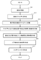
- FIG. 8 is a flowchart showing a schematic content and procedure of the method for manufacturing the wiring board 10 according to the present embodiment.
- step S11 a core part composed of the substrate 100 or the like is formed.
- a double-sided copper-clad laminate 1000 is prepared as a starting material.
- the double-sided copper clad laminate 1000 includes a substrate 100 (core substrate), a copper foil 1001 formed on the first surface F1 of the substrate 100, a copper foil 1002 formed on the second surface F2 of the substrate 100, Consists of In the present embodiment, at this stage, the substrate 100 is made of a glass epoxy that is completely cured.
- a hole 1003a is formed by irradiating the double-sided copper-clad laminate 1000 with a laser from the first surface F1 side using, for example, a CO 2 laser, and the laser is emitted from the second surface F2 side. Is irradiated to the double-sided copper-clad laminate 1000 to form a hole 1003b.
- the hole 1003a and the hole 1003b are formed at substantially the same position in the XY plane and are finally connected to form a through hole 300a penetrating the double-sided copper-clad laminate 1000.
- the shape of the through hole 300a is, for example, an hourglass shape (a drum shape).
- the boundary between the hole 1003a and the hole 1003b corresponds to the constricted portion 300c (FIG. 1).
- the laser irradiation on the first surface F1 and the laser irradiation on the second surface F2 may be performed simultaneously or may be performed one side at a time.
- Undesirable conduction (short circuit) is suppressed by desmear.
- the surfaces of the copper foils 1001 and 1002 may be blackened prior to laser irradiation.
- the through hole 300a may be formed by a method other than laser, such as drilling or etching. However, fine processing is easy with laser processing.
- copper plating 1004 is formed on the copper foils 1001 and 1002 and in the through holes 300a by, for example, panel plating. Specifically, first, electroless plating is performed, and then plating 1004 is formed by performing electrolytic plating using the electroless plating film as a seed layer using a plating solution. Thereby, the through hole 300a is filled with the plating 1004, and the through hole conductor 300b is formed.
- each conductor layer formed on the first surface F1 and the second surface F2 of the substrate 100 is performed using, for example, an etching resist and an etching solution.
- each conductor layer is covered with an etching resist having a pattern corresponding to the conductor layers 301 and 302, and a portion of each conductor layer that is not covered with the etching resist (part exposed at the opening of the etching resist) Remove by etching.
- conductor layers 301 and 302 are formed on the first surface F1 and the second surface F2 of the substrate 100, respectively.
- the conductor layers 301 and 302 each have a three-layer structure of, for example, a copper foil (lower layer), an electroless copper plating (intermediate layer), and an electrolytic copper plating (upper layer).
- etching is not limited to wet, but may be dry. Further, it is considered preferable to roughen the surfaces of the conductor layers 301 and 302 by etching or the like as necessary. Further, an alignment mark used in a subsequent process (such as a process of arranging the electronic components 200a and 200b) may be formed on the conductor layer 301 or 302.
- step S12 of FIG. 8 for example, as shown in FIG. 10, the substrate 100 is irradiated with laser light from the first surface F1 side to form the cavity R10.
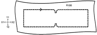
- the substrate 100 is irradiated with laser light from the first surface F1 side to form the cavity R10.
- the region R100 corresponding to the cavity R10 in the substrate 100 is Cut from the part.
- the laser irradiation angle is set to be substantially perpendicular to the first surface F1 of the substrate 100, for example.
- the conductor layer 301 on the substrate 100 is removed corresponding to the shape of the cavity R10 as shown in FIG. 11B or along the laser irradiation path as shown in FIG. 11C. It may be left. By doing so, the position and shape of the cavity R10 are clarified, and alignment of laser irradiation becomes easy.
- the cavity R10 is formed by the laser beam irradiation as shown in FIG.
- the amount of processing by the laser decreases toward the second surface F2 side, and the cavity R10 is moved from the first surface F1 to the second surface F2.
- the width is reduced toward the surface F2 side.
- the cut surface of the substrate 100 becomes a tapered surface.
- the projections P21 and P22 are formed on the wall surface of the cavity R10 by moving the laser light.
- all of the wall surfaces of the cavity R10 are formed by the cut surface (tapered surface) of the substrate 100.
- the cavity R10 thus formed becomes a storage space for the electronic components 200a and 200b.
- the cavity R10 is formed by a laser, the cavity R10 having a tapered wall surface can be easily obtained.
- the method of forming the cavity R10 is not limited to the laser, and may be arbitrary, and may be formed by a mold, for example.
- the electronic components 200a and 200b are placed in the cavity R10 of the substrate 100 in step S13 of FIG.
- a carrier 1005 made of, for example, PET (polyethylene terephthalate) is provided on one side (for example, the second surface F2) of the substrate 100. Thereby, one opening of the cavity R10 (hole) is closed by the carrier 1005.
- the carrier 1005 is made of an adhesive sheet (for example, a tape) and has adhesiveness on the substrate 100 side.
- the carrier 1005 is bonded to the second surface F2 side (the conductor layer 302 and the like) of the substrate 100 by lamination, for example.
- the electronic components 200a and 200b are inserted into the cavity R10 from the opposite side (Z1 side) to the opening where the cavity R10 (hole) is blocked.
- Each of the electronic components 200a and 200b is inserted into the cavity R10 by, for example, a component mounter.
- each of the electronic components 200a and 200b is held by a vacuum chuck or the like, conveyed to the upper side (Z1 side) of the cavity R10, and then descends along the vertical direction, and is put into the cavity R10.
- the electronic components 200a and 200b are placed on the carrier 1005 (adhesive sheet).
- step S14 of FIG. 8 the side opposite to the opening where the cavity R10 (hole) is blocked (Z1 side), that is, on the first surface F1 of the substrate 100 and the electronic component 200a.
- the semi-cured insulating layer 101 is formed on the third surface F3 of 200b.
- a copper foil 1006 is formed on the insulating layer 101.
- the insulating layer 101 is made of, for example, a prepreg of an epoxy resin having thermosetting properties.
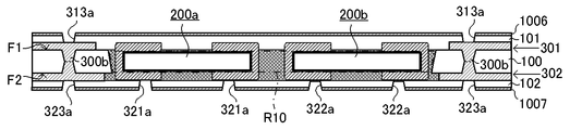
- FIG. 17 by pressing the insulating layer 101 in a semi-cured state, the resin flows out from the insulating layer 101 and flows into the cavity R10. Accordingly, as shown in FIG. 18, insulation is provided between the electronic components 200a and 200b in the cavity R10 and the substrate 100 (region R1) and between the electronic component 200a and the electronic component 200b (region R2).
- the body 101a (resin constituting the insulating layer 101) is filled.
- the filling resin (insulator 101a) and the electronic components 200a and 200b are temporarily welded. Specifically, the holding resin is developed to a degree that can support the electronic components 200a and 200b in the filled resin by heating. As a result, the electronic components 200a and 200b supported by the carrier 1005 are supported by the filling resin. Thereafter, the carrier 1005 is removed.
- the insulator 101a filling resin
- the insulating layer 101 are only semi-cured and not completely cured.
- the invention is not limited to this.
- the insulator 101a and the insulating layer 101 may be completely cured at this stage.
- the insulating layer 102 and the copper foil 1007 are formed on the second surface F ⁇ b> 2 of the substrate 100.
- the electrodes 210 and 220 of the electronic components 200a and 200b are each covered with an insulating layer 102.
- the insulating layers 101 and 102 are cured by heating.
- the resin filled in the cavity R10 is cured after removing the adhesive sheet (carrier 1005), the insulating layers 101 and 102 can be cured simultaneously. Then, by simultaneously curing the insulating layers 101 and 102 on both sides, warpage of the substrate 100 is suppressed, so that the substrate 100 can be easily thinned.
- step S16 of FIG. 8 a via conductor and a conductor layer are formed.
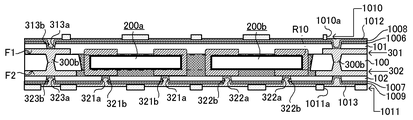
- holes 313a are formed in the insulating layer 101 and the copper foil 1006, for example, by laser, and holes 321a to 323a (respectively, via holes) are formed in the insulating layer 102 and the copper foil 1007. .
- the hole 313a penetrates the copper foil 1006 and the insulating layer 101, and each of the holes 321a to 323a penetrates the copper foil 1007 and the insulating layer 102.
- the hole 321a reaches the electrode 210 or 220 of the electronic component 200a, and the hole 322a reaches the electrode 210 or 220 of the electronic component 200b.
- Each of the holes 313a and 323a reaches the conductor layers 301 and 302 immediately above the through-hole conductor 300b. Then, desmear is performed as needed.
- copper electroless plating films 1008 and 1009 are formed on the copper foils 1006 and 1007 and in the holes 313a and 321a to 323a by chemical plating, for example (see FIG. 21).
- a catalyst made of palladium or the like may be adsorbed on the surfaces of the insulating layers 101 and 102, for example, by dipping.
- a plating resist 1011 having an opening 1011a is formed on the electrolytic plating film 1009) (see FIG. 21).
- the openings 1010a and 1011a have patterns corresponding to the conductor layers 110 and 120 (FIG. 22), respectively.
- copper electrolytic plating 1012 and 1013 are formed in the openings 1010a and 1011a of the plating resists 1010 and 1011 by, for example, pattern plating. Specifically, copper that is a material to be plated is connected to the anode, and electroless plating films 1008 and 1009 that are materials to be plated are connected to the cathode and immersed in a plating solution. Then, a direct current voltage is applied between the two electrodes to pass a current, and copper is deposited on the surfaces of the electroless plating films 1008 and 1009.
- the holes 313a and 321a to 323a are filled with the electroless plating films 1008 and 1009 and the electrolytic plating 1012 and 1013, respectively, and via conductors 313b and 321b to 323b made of, for example, copper plating are formed.
- the plating resists 1010 and 1011 are removed with, for example, a predetermined stripping solution, and then the unnecessary electroless plating films 1008 and 1009 and the copper foils 1006 and 1007 are removed, as shown in FIG. 110 and the conductor layer 120 are formed.
- the seed layer for electrolytic plating is not limited to the electroless plating film, and a sputtered film or the like may be used as the seed layer instead of the electroless plating films 1008 and 1009.
- a solder resist 11 having an opening 11a and a solder resist 12 having an opening 12a are formed on the insulating layers 101 and 102, respectively (see FIG. 1).
- the conductor layers 110 and 120 are covered with solder resists 11 and 12 except for predetermined portions (pads P11 and P12, etc.) located in the openings 11a and 12a, respectively.
- the solder resists 11 and 12 can be formed by, for example, screen printing, spray coating, roll coating, or lamination.
- the corrosion resistance made of, for example, a Ni / Au film on the conductor layers 110 and 120, specifically, the surfaces of the pads P11 and P12 (see FIG. 1) not covered with the solder resists 11 and 12, respectively.
- the corrosion-resistant layer which consists of an organic protective film by performing OSP process.
- a build-up portion composed of the insulating layer 101 and the conductor layer 110 is formed on the first surface F1 of the substrate 100, and composed of the insulating layer 102 and the conductor layer 120 on the second surface F2 of the substrate 100.
- the build-up part is formed.
- the wiring board 10 (FIG. 1) of this embodiment is completed.
- an electrical test checking of capacitance value, insulation, etc. of the electronic components 200a and 200b is performed.
- the manufacturing method of the present embodiment is suitable for manufacturing the wiring board 10. With such a manufacturing method, it is considered that a good wiring board 10 can be obtained at low cost.
- the wiring board 10 of this embodiment can be electrically connected to, for example, an electronic component or another wiring board.
- an electronic component 400 for example, an IC chip
- the wiring board 10 can be mounted on another wiring board 500 (for example, a mother board) by the pad P11.
- the wiring board 10 of this embodiment can be used as a circuit board of a mobile phone, for example.
- the shapes of the electronic components 200a and 200b and the cavity R10 are arbitrary.
- the opening shape of the cavity R10 may be substantially oval.
- the planar shape of the electronic components 200a and 200b and the opening shape of the cavity R10 may be substantially circles (substantially perfect circles), and may be substantially many other than substantially rectangular, such as substantially squares, substantially regular hexagons, and substantially regular octagons. It may be square.
- the shape of the polygonal corner is arbitrary, and may be rounded, for example, substantially right angle, acute angle, obtuse angle.
- the shape of the protrusions P21 and P22 is also arbitrary.
- the planar shape of the protrusions P21 and P22 may be a flask shape.
- each of the protrusions P21 and P22 has a skirt that becomes narrower toward the tip at a certain rate, and a rectangular tip.
- the protrusions P21 and P22 having such a shape are excellent in terms of laser workability and strength.
- the width P31 of the protrusion P21 is about 80 ⁇ m
- the width D311 of the skirt is about 30 ⁇ m
- the width D312 of the tip is about 20 ⁇ m.
- the protrusion amount D32 of the protrusion P21 is about 125 ⁇ m.
- the length D321 of the skirt portion is about 40 ⁇ m
- the length D322 of the tip portion is about 85 ⁇ m.
- Each dimension in the projection part P22 is the same as that of the projection part P21, for example.
- the planar shape of the protrusions P21 and P22 may be a quadrangle (for example, a rectangle).
- each of the protrusions P21 and P22 has a substantially constant width throughout. Protrusions P21 and P22 having such a shape are excellent in terms of laser workability and component mountability.
- the width D31 of the protrusion P21 is about 20 ⁇ m, and the protrusion amount D32 of the protrusion P21 is about 290 ⁇ m.
- the width D31 of the protrusion P21 is about 20 ⁇ m, and the protrusion amount D32 of the protrusion P21 is about 125 ⁇ m.
- Each dimension in the projection part P22 is the same as that of the projection part P21, for example.
- the planar shape of the protrusions P21 and P22 may be a wedge shape (for example, a trapezoid).
- the protrusions P21 and P22 are each narrowed toward the tip at a constant rate throughout.
- the protrusions P21 and P22 having such a shape are excellent in terms of laser workability and strength.
- the width D31 of the protrusion P21 is about 40 ⁇ m
- the width D311 of the skirt is about 10 ⁇ m
- the width D312 of the tip is about 20 ⁇ m
- the protrusion amount D32 of the protrusion P21 is about 125 ⁇ m. is there.
- the width D31 of the protrusion P21 is about 60 ⁇ m
- the width D311 of the skirt is about 20 ⁇ m
- the width D312 of the tip is about 20 ⁇ m
- the protrusion amount D32 of the protrusion P21 is about 125 ⁇ m.
- the width P31 of the protrusion P21 is about 80 ⁇ m
- the width D311 of the skirt is about 30 ⁇ m
- the width D312 of the tip is about 20 ⁇ m
- the protrusion amount D32 of the protrusion P21 is about 125 ⁇ m.
- Each dimension in the projection part P22 is the same as that of the projection part P21, for example.
- the widths of the protrusions P21 and P22 are narrowed at a constant rate, but the present invention is not limited to this, and the degree of narrowing may be smaller toward the tip. Moreover, as shown in FIG. 28, the tips P201 and P202 may be sharp. In the example of FIG. 28, the planar shapes of the protrusions P21 and P22 are triangular.
- planar shapes of the protrusions P21 and P22 may be substantially semicircular, and their tips P201 and P202 may be rounded.
- planar shape of the projections P21 and P22 may be substantially W-shaped, and each of the projections P21 and P22 may have a plurality of tips P201 or P202.
- the edge P211 of the protrusion P21 and the edge P221 of the protrusion P22 may not be tapered.
- a step may be formed at the edge P211 of the protrusion P21 and the edge P221 of the protrusion P22.
- a step may be formed in the edge P211 of the protrusion P21 and the edge P221 of the protrusion P22, and a part (for example, the lower stage) may be tapered.
- a part for example, the lower stage
- not only the edge but also the entire protrusions P21 and P22 may be tapered.
- Arrangement of the electronic device arranged in the cavity R10 (opening) is arbitrary.
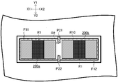
- the electronic components 200a and 200b may be arranged in the short direction.
- the number of electronic devices arranged in the cavity R10 (opening) is arbitrary as long as it is plural.
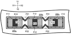
- three electronic components 200a, 200b, and 200c may be accommodated in the cavity R10.
- the tips of the protrusions protrusions P21 and P22
- the projecting part P21 and the projecting part P22 are formed on opposing wall surfaces at a position that divides the cavity R10 into approximately three equal parts, and the tip ends face each other to make a pair.
- the width of the cavity R10 is narrowed, and the space of the cavity R10 is divided into three spaces for accommodating the electronic components 200a to 200c.
- the electronic component 200a is surrounded by the wall surface F11 of the non-projection part, the tip surface F21 of the projection part P21, and the tip surface F22 of the projection part P22.
- the electronic component 200b is surrounded by the wall surface F12 of the non-projection portion, the tip surface F21 of the projection portion P21, and the tip surface F22 of the projection portion P22.
- the electronic component 200c is surrounded by the wall surface F13 of the non-projection part, the tip surface F21 of the projection part P21, and the tip surface F22 of the projection part P22.
- each electronic component 200a, 200b, 200c, and 200d may be accommodated in the cavity R10.
- the tip of the protrusion P21 enters between the adjacent electronic component 200a and the electronic component 200b
- the tip of the protrusion P22 enters between the adjacent electronic component 200b and the electronic component 200c
- the tip of the protrusion P23 enters between the adjacent electronic component 200c and the electronic component 200d
- the tip of the protrusion P24 enters between the adjacent electronic component 200d and the electronic component 200a.
- the electronic components 200a to 200d are surrounded by the wall surface of the cavity R10 (the cut surface of the substrate 100). However, each of the electronic components 200a to 200d is not surrounded by the wall surface of the cavity R10. In contrast, in the example of FIG. 35, an isolated island-shaped block P30 as a part of the substrate 100 is provided between the electronic components 200a to 200d, so that each of the electronic components 200a to 200d cuts the substrate 100. Surrounded by a face. Specifically, the electronic component 200a is surrounded by the wall surface F11 of the non-projection portion, the tip surface F21 of the projection portion P21, the tip surface F24 of the projection portion P24, and the side surface F30 of the block P30.
- the electronic component 200b is surrounded by the wall surface F12 of the non-projection part, the tip surface F21 of the projection part P21, the tip surface F22 of the projection part P22, and the side surface F30 of the block P30.
- the electronic component 200c is surrounded by the wall surface F13 of the non-projection part, the tip surface F22 of the projection part P22, the tip surface F23 of the projection part P23, and the side surface F30 of the block P30.
- the electronic component 200d is surrounded by the wall surface F14 of the non-projection portion, the tip surface F23 of the projection portion P23, the tip surface F24 of the projection portion P24, and the side surface F30 of the block P30. Since each of the electronic components 200a to 200d is surrounded by the cut surface of the substrate 100, the positional deviation of the electronic components 200a to 200d can be more reliably suppressed.
- the pair of protrusions are formed on the opposing wall surfaces of the cavity R10 (opening) and the tips face each other.
- the protrusion P21 may be formed on the wall surface of the cavity R10, and the protrusion may not be formed on the opposite wall surface. If the tip of the protrusion is inserted between the adjacent electronic devices at least at one place, it is possible to prevent a short circuit between the adjacent electronic devices.
- the protrusion is formed as a part of the substrate 100, but the protrusion may be formed separately from the substrate 100.
- the substrate 100 and the protrusions P21 and P22 are formed separately, and the protrusions P21 and P22 are connected to the wall surface of the cavity R10 (the cut surface of the substrate 100) later by an adhesive or the like. May be.
- the electronic components 200a and 200b have the single-sided via structure, but the present invention is not limited to this.
- a wiring board having via conductors 311b, 312b, 321b, and 322b electrically connected to the electrodes 210 and 220 of the electronic components 200a and 200b on both sides of the electronic components 200a and 200b may be used. .
- What is built in the wiring board 10 is not limited to a capacitor, and may be other electronic components.
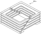
- an electronic component 601a made of an inductor and an electronic component 601b made of a capacitor may be accommodated in one cavity R10.
- the tip P201 of the projection P21 and the tip P202 of the projection P22 enter between the adjacent electronic components 601a and 601b (see FIGS. 4A and 4B), the short circuit (conduction) between the electronic components 601a and 601b is suppressed. Is done.
- the electronic component 601a is composed of two one-turn inductors as shown in FIG. 39B, for example.
- Each inductor is formed in a spiral shape and a substantially circular shape in plan view (specifically, a substantially square shape) by a four-layer conductor pattern.
- the inductors are connected in parallel to each other.
- the wiring board 10 is not limited to electronic components, and may be other wiring boards.
- the wiring boards 602a and 602b may be accommodated in one cavity R10.
- the tip P201 of the projection P21 and the tip P202 of the projection P22 enter between the adjacent wiring boards 602a and 602b (see FIGS. 4A and 4B)
- the short circuit (conduction) between the wiring boards 602a and 602b is suppressed. Is done.
- the pad (external connection terminal) of the wiring board 602a is electrically connected to the conductor layers 110 and 120 via the via conductors 311b and 321b.
- the pads (external connection terminals) of the wiring board 602b are electrically connected to the conductor layers 110 and 120 through the via conductors 312b and 322b.
- the wiring boards 602a and 602b have conductors at a higher density than the wiring board 10, for example, because each conductor layer has a fine conductor pattern, or because an interlayer insulating layer between conductor layers is thin. It is preferable.
- the double-sided wiring board (wiring board 10) having the conductor layers on both sides of the core substrate is shown, but the present invention is not limited to this.
- a single-sided wiring board having a conductor layer only on one side of the core substrate (substrate 100) may be used.
- electronic components 603a and 603b made of IC chips are accommodated in one cavity R10.
- the cavity R10 (the storage space for the electronic components 200a and 200b) may be a hole (concave portion) that does not penetrate the substrate 100.
- the thickness of the substrate 100 and the thickness of the electronic components 200a and 200b are substantially the same is shown, but the present invention is not limited to this.
- the thickness of the substrate 100 may be larger than the thickness of the electronic components 603a and 603b.
- a wiring board having two or more build-up layers on one side of the core substrate may be used. Further, the number of buildup layers may be different between the first surface F1 side of the substrate 100 and the second surface F2 side of the substrate 100. However, in order to relieve stress, it is preferable to increase the symmetry of the front and back by making the number of buildup layers the same on the first surface F1 side of the substrate 100 and the second surface F2 side of the substrate 100. Conceivable.
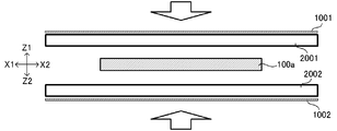
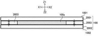
- the substrate 100 may be an insulating substrate containing a metal plate 100a (for example, copper foil). In such a substrate 100, heat dissipation is improved by the metal plate 100a.
- the via conductor 100b reaching the metal plate 100a is formed on the substrate 100, and the metal plate 100a and the ground line (conductor patterns included in the conductor layers 301 and 302) are mutually connected via the via conductor 100b. Electrically connected.
- the planar shape of the metal plate 100a is arbitrary, and may be a quadrangle or a circle.
- FIG. 42 An example of a method for manufacturing the substrate 100 (core substrate) shown in FIG. 42 will be described with reference to FIGS. 43A and 43B.
- insulating layers 2001 and 2002 are disposed so as to sandwich a metal plate 100a made of, for example, copper foil, copper foil 1001 is further disposed on insulating layer 2001, and copper foil is disposed on insulating layer 2002. 1002 is arranged.
- a metal plate 100a made of, for example, copper foil
- copper foil 1001 is further disposed on insulating layer 2001
- copper foil is disposed on insulating layer 2002.
- 1002 is arranged.
- Each of the insulating layers 2001 and 2002 is made of, for example, a glass prepreg.
- the configuration of the wiring board 10 (in particular, the type, performance, dimensions, material, shape, number of layers, arrangement, etc. of the components) can be arbitrarily changed without departing from the spirit of the present invention.
- the shape of the electrode of the chip capacitor disposed in the cavity R10 (opening) is not limited to the U-shape, and for example, the capacitor body 201 may be sandwiched between flat electrode pairs.
- the type of the electronic device arranged in the cavity R10 (opening) is arbitrary.
- any electronic component such as an active component such as an IC circuit or a wiring board can be adopted.
- Each via conductor is not limited to a filled conductor, and may be a conformal conductor, for example.
- the electronic device arranged in the cavity R10 may not be mounted by via connection (via conductor) but may be mounted by other methods such as wire bonding connection.
- the method of manufacturing the wiring board is not limited to the order and contents shown in FIG. 8, and the order and contents can be arbitrarily changed without departing from the spirit of the present invention. Moreover, you may omit the process which is not required according to a use etc.
- each conductor layer is arbitrary.
- processing may be performed by wet or dry etching.
- processing by etching it is considered preferable to protect portions that are not desired to be removed in advance with a resist or the like.
- planar shape of the protrusion shown in any of FIGS. 25 to 30, the cross-sectional shape of the protrusion shown in any of FIGS. 31A to 31D, and the number of electronic devices shown in any of FIGS. And arrangement may be arbitrarily combined.
- the wiring board according to the present invention is suitable for forming an electric circuit of a built-in electronic component. Moreover, the manufacturing method of the wiring board which concerns on this invention is suitable for manufacture of a wiring board.
Landscapes
- Engineering & Computer Science (AREA)
- Microelectronics & Electronic Packaging (AREA)
- Manufacturing & Machinery (AREA)
- Production Of Multi-Layered Print Wiring Board (AREA)
Abstract
Description
11、12 ソルダーレジスト
11a、12a 開口部
100 基板
100a 金属板
100b ビア導体
101、102 絶縁層
101a 絶縁体
110、120 導体層
200a~200d 電子部品
201 コンデンサ本体
210、220 電極
210a、220a 上部
210b、220b 側部
210c、220c 下部
211~214、221~224 導体層
231~239 誘電層
300a スルーホール
300b スルーホール導体
300c 括れ部
301、302 導体層
313a 孔
311b~313b ビア導体
321a~323a 孔
321b~323b ビア導体
400 電子部品
500 配線板
601a、601b 電子部品
602a、602b 配線板
603a、603b 電子部品
1000 両面銅張積層板
1001、1002 銅箔
1003a、1003b 孔
1004 めっき
1005 キャリア
1006、1007 銅箔
1008、1009 無電解めっき膜
1010、1011 レジスト
1010a、1011a 開口部
2001~2003 絶縁層
F11~F14 壁面
F21~F24 先端面
F30 側面
P11、P12 パッド
P21~P24 突起部
P30 ブロック
P201、P202 先端
P211、P221 縁部
R1、R2 領域
R10 キャビティ
R100 領域
Claims (20)
- 開口部を有する基板と、
1つの前記開口部に配置される複数の電子デバイスと、
前記基板上及び前記電子デバイス上に配置される絶縁層と、
前記絶縁層上に配置される導体層と、
を有する配線板において、
前記開口部の壁面に突起が形成され、
少なくとも一箇所で、隣り合う前記電子デバイスの間に前記突起の先端が入り込んでいる、
ことを特徴とする配線板。 - 前記隣り合う電子デバイスの間に前記突起の先端が入り込むことによって、それら電子デバイスが離間している、
ことを特徴とする請求項1に記載の配線板。 - 前記突起の先端面は、前記基板の切断面からなる、
ことを特徴とする請求項1又は2に記載の配線板。 - 前記突起の先端面は、テーパ面からなる、
ことを特徴とする請求項1乃至3のいずれか一項に記載の配線板。 - 先端同士が向き合う前記突起の対が形成される、
ことを特徴とする請求項1乃至4のいずれか一項に記載の配線板。 - 前記突起の対は、前記開口部を略等分する位置の対向する壁面に形成される、
ことを特徴とする請求項5に記載の配線板。 - 前記複数の電子デバイスの各々は、前記基板の切断面によって囲まれる、
ことを特徴とする請求項1乃至6のいずれか一項に記載の配線板。 - 前記複数の電子デバイスの各々を囲む前記基板の切断面の全てが、テーパ面からなる、
ことを特徴とする請求項7に記載の配線板。 - 前記隣り合う電子デバイスの少なくとも一方が、上面と側面と下面とにわたって形成される電極を有するチップコンデンサである、
ことを特徴とする請求項1乃至8のいずれか一項に記載の配線板。 - 前記隣り合う電子デバイスの少なくとも一方が、インダクタである、
ことを特徴とする請求項1乃至9のいずれか一項に記載の配線板。 - 前記基板と前記電子デバイスとの間、及び、前記電子デバイス同士の間にはそれぞれ、前記絶縁層を構成する樹脂が充填される、
ことを特徴とする請求項1乃至10のいずれか一項に記載の配線板。 - 前記電子デバイスの直上に、外部接続端子を有する、
ことを特徴とする請求項1乃至11のいずれか一項に記載の配線板。 - 前記絶縁層に形成された孔内に導体が形成されてなるビア導体を有し、
前記導体層と前記電子デバイスの電極とは、前記ビア導体を介して、互いに電気的に接続される、
ことを特徴とする請求項1乃至12のいずれか一項に記載の配線板。 - 前記基板は、金属板を内蔵する絶縁基板である、
ことを特徴とする請求項1乃至13のいずれか一項に記載の配線板。 - 基板を準備することと、
前記基板に、壁面に突起を有する開口部を形成することと、
少なくとも一箇所で、隣り合う電子デバイスの間に前記突起の先端が入り込むように、複数の電子デバイスを1つの前記開口部に配置することと、
前記基板上及び前記電子デバイス上に絶縁層を形成することと、
前記絶縁層上に導体層を形成することと、
を含む、
配線板の製造方法。 - 前記基板を切断することにより、前記突起を形成する、
ことを特徴とする請求項15に記載の配線板の製造方法。 - レーザにより前記基板を切断する、
ことを特徴とする請求項16に記載の配線板の製造方法。 - 先端同士が向き合うように、前記突起の対を形成する、
ことを特徴とする請求項15乃至17のいずれか一項に記載の配線板の製造方法。 - 前記基板と前記電子デバイスとの間、及び、前記電子デバイス同士の間にそれぞれ、前記絶縁層を構成する樹脂を充填することを含む、
ことを特徴とする請求項15乃至18のいずれか一項に記載の配線板の製造方法。 - 前記絶縁層に孔を形成することと、
前記孔内に導体が形成されてなるビア導体を形成することと、
前記導体層と前記電子デバイスの電極とを、前記ビア導体を介して、互いに電気的に接続することと、
を含む、
ことを特徴とする請求項15乃至19のいずれか一項に記載の配線板の製造方法。
Priority Applications (3)
| Application Number | Priority Date | Filing Date | Title |
|---|---|---|---|
| KR1020137024849A KR101422437B1 (ko) | 2011-05-13 | 2012-04-25 | 배선판 및 그 제조 방법 |
| CN201280023363.6A CN103563498B (zh) | 2011-05-13 | 2012-04-25 | 电路板及其制造方法 |
| JP2013515062A JP5600803B2 (ja) | 2011-05-13 | 2012-04-25 | 配線板及びその製造方法 |
Applications Claiming Priority (2)
| Application Number | Priority Date | Filing Date | Title |
|---|---|---|---|
| US201161485835P | 2011-05-13 | 2011-05-13 | |
| US61/485,835 | 2011-05-13 |
Publications (1)
| Publication Number | Publication Date |
|---|---|
| WO2012157426A1 true WO2012157426A1 (ja) | 2012-11-22 |
Family
ID=47141737
Family Applications (1)
| Application Number | Title | Priority Date | Filing Date |
|---|---|---|---|
| PCT/JP2012/061143 Ceased WO2012157426A1 (ja) | 2011-05-13 | 2012-04-25 | 配線板及びその製造方法 |
Country Status (6)
| Country | Link |
|---|---|
| US (2) | US8693209B2 (ja) |
| JP (1) | JP5600803B2 (ja) |
| KR (1) | KR101422437B1 (ja) |
| CN (1) | CN103563498B (ja) |
| TW (1) | TWI429345B (ja) |
| WO (1) | WO2012157426A1 (ja) |
Cited By (13)
| Publication number | Priority date | Publication date | Assignee | Title |
|---|---|---|---|---|
| JP2014107498A (ja) * | 2012-11-29 | 2014-06-09 | Murata Mfg Co Ltd | 部品内蔵樹脂多層基板およびその製造方法 |
| JP2014110423A (ja) * | 2012-12-04 | 2014-06-12 | Samsung Electro-Mechanics Co Ltd | 電子部品組込み基板及びその製造方法 |
| CN104010448A (zh) * | 2013-02-21 | 2014-08-27 | 味之素株式会社 | 部件内置型布线基板的制造方法以及半导体装置 |
| JP2014187360A (ja) * | 2013-02-21 | 2014-10-02 | Ajinomoto Co Inc | 部品内蔵回路板の製造方法、および半導体装置 |
| WO2014185438A1 (ja) * | 2013-05-17 | 2014-11-20 | 株式会社村田製作所 | 部品内蔵多層基板の製造方法および部品内蔵多層基板 |
| JP2015118954A (ja) * | 2013-12-16 | 2015-06-25 | 味の素株式会社 | 部品内蔵基板の製造方法、および半導体装置 |
| JP2015135940A (ja) * | 2013-12-16 | 2015-07-27 | 味の素株式会社 | 部品内蔵基板の製造方法および半導体装置 |
| JP2015144151A (ja) * | 2014-01-31 | 2015-08-06 | 京セラサーキットソリューションズ株式会社 | 配線基板の製造方法 |
| JP2015170669A (ja) * | 2014-03-05 | 2015-09-28 | 新光電気工業株式会社 | 配線基板、及び、配線基板の製造方法 |
| JP2015170670A (ja) * | 2014-03-05 | 2015-09-28 | 新光電気工業株式会社 | 配線基板、及び、配線基板の製造方法 |
| JP2015191996A (ja) * | 2014-03-28 | 2015-11-02 | 京セラサーキットソリューションズ株式会社 | 印刷配線板およびその製造方法 |
| US10080293B2 (en) | 2016-08-05 | 2018-09-18 | Shinko Electric Industries Co., Ltd. | Electronic component-embedded board and electronic component device |
| US10321574B2 (en) | 2016-10-04 | 2019-06-11 | Shinko Electric Industries Co., Ltd. | Electronic component-embedded substrate and electronic component device |
Families Citing this family (32)
| Publication number | Priority date | Publication date | Assignee | Title |
|---|---|---|---|---|
| US8908387B2 (en) | 2011-10-31 | 2014-12-09 | Ibiden Co., Ltd. | Wiring board and method for manufacturing the same |
| US9439289B2 (en) | 2012-01-12 | 2016-09-06 | Ibiden Co., Ltd. | Wiring board and method for manufacturing the same |
| US9113574B2 (en) * | 2012-10-25 | 2015-08-18 | Ibiden Co., Ltd. | Wiring board with built-in electronic component and method for manufacturing the same |
| JP2015038912A (ja) * | 2012-10-25 | 2015-02-26 | イビデン株式会社 | 電子部品内蔵配線板およびその製造方法 |
| JP2014107431A (ja) * | 2012-11-28 | 2014-06-09 | Ibiden Co Ltd | 電子部品内蔵配線板、及び、電子部品内蔵配線板の製造方法 |
| KR101420526B1 (ko) * | 2012-11-29 | 2014-07-17 | 삼성전기주식회사 | 전자부품 내장기판 및 그 제조방법 |
| DE112013006630T5 (de) * | 2013-02-08 | 2015-10-22 | Fujikura Ltd. | Platte mit eingebetteter Komponente und Verfahren zum Herstellen derselben |
| KR101514518B1 (ko) * | 2013-05-24 | 2015-04-22 | 삼성전기주식회사 | 전자부품 내장 인쇄회로기판 및 그 제조방법 |
| TWI634826B (zh) * | 2013-06-17 | 2018-09-01 | 味之素股份有限公司 | Manufacturing method of built-in component wiring board, built-in component insulating substrate, built-in component two-layer wiring substrate, and semiconductor device |
| US9209151B2 (en) * | 2013-09-26 | 2015-12-08 | General Electric Company | Embedded semiconductor device package and method of manufacturing thereof |
| JP2015159153A (ja) * | 2014-02-21 | 2015-09-03 | イビデン株式会社 | 電子部品内蔵多層配線板 |
| JP2015220281A (ja) * | 2014-05-15 | 2015-12-07 | イビデン株式会社 | プリント配線板 |
| JP2015231003A (ja) * | 2014-06-06 | 2015-12-21 | イビデン株式会社 | 回路基板および回路基板の製造方法 |
| JP6393566B2 (ja) * | 2014-09-17 | 2018-09-19 | 新光電気工業株式会社 | 配線基板、半導体装置及び配線基板の製造方法 |
| KR102139755B1 (ko) * | 2015-01-22 | 2020-07-31 | 삼성전기주식회사 | 인쇄회로기판 및 그 제조방법 |
| US9837484B2 (en) * | 2015-05-27 | 2017-12-05 | STATS ChipPAC Pte. Ltd. | Semiconductor device and method of forming substrate including embedded component with symmetrical structure |
| US9743526B1 (en) * | 2016-02-10 | 2017-08-22 | International Business Machines Corporation | Wiring board with stacked embedded capacitors and method of making |
| US9887167B1 (en) * | 2016-09-19 | 2018-02-06 | Advanced Semiconductor Engineering, Inc. | Embedded component package structure and method of manufacturing the same |
| JP6751910B2 (ja) * | 2016-10-05 | 2020-09-09 | パナソニックIpマネジメント株式会社 | 多層プリント配線板、多層プリント配線板の製造方法 |
| KR101963282B1 (ko) * | 2016-12-16 | 2019-03-28 | 삼성전기주식회사 | 팬-아웃 반도체 패키지 |
| KR101901712B1 (ko) * | 2017-10-27 | 2018-09-27 | 삼성전기 주식회사 | 팬-아웃 반도체 패키지 |
| KR101942744B1 (ko) * | 2017-11-03 | 2019-01-28 | 삼성전기 주식회사 | 팬-아웃 반도체 패키지 |
| US10347586B2 (en) | 2017-11-30 | 2019-07-09 | Samsung Electro-Mechanics Co., Ltd. | Fan-out semiconductor package |
| KR102039712B1 (ko) * | 2017-11-30 | 2019-11-26 | 삼성전자주식회사 | 팬-아웃 반도체 패키지 |
| KR101912290B1 (ko) * | 2017-12-06 | 2018-10-29 | 삼성전기 주식회사 | 팬-아웃 반도체 패키지 |
| KR102679250B1 (ko) * | 2018-09-12 | 2024-06-28 | 엘지이노텍 주식회사 | 연성 회로기판 및 이를 포함하는 칩 패키지, 및 이를 포함하는 전자 디바이스 |
| TWI694756B (zh) * | 2018-12-27 | 2020-05-21 | 欣興電子股份有限公司 | 一種具有散熱塊的電路板及其製造方法 |
| US11445596B2 (en) | 2018-12-27 | 2022-09-13 | Unimicron Technology Corp. | Circuit board having heat-dissipation block and method of manufacturing the same |
| JP7279538B2 (ja) * | 2019-06-19 | 2023-05-23 | 富士フイルムビジネスイノベーション株式会社 | 発光装置 |
| CN112770495B (zh) * | 2019-10-21 | 2022-05-27 | 宏启胜精密电子(秦皇岛)有限公司 | 全向内埋模组及制作方法、封装结构及制作方法 |
| CN113130408A (zh) | 2019-12-31 | 2021-07-16 | 奥特斯奥地利科技与系统技术有限公司 | 部件承载件及制造部件承载件的方法 |
| US20250070001A1 (en) * | 2023-08-24 | 2025-02-27 | Qualcomm Incorporated | Device including substrate with passive electronic component embedded therein |
Citations (5)
| Publication number | Priority date | Publication date | Assignee | Title |
|---|---|---|---|---|
| JP2002118368A (ja) * | 2000-07-31 | 2002-04-19 | Ngk Spark Plug Co Ltd | 配線基板およびその製造方法 |
| JP2005072415A (ja) * | 2003-08-27 | 2005-03-17 | Dainippon Printing Co Ltd | 部品内蔵配線板の製造方法、部品内蔵配線板 |
| JP2005311249A (ja) * | 2004-04-26 | 2005-11-04 | Taiyo Yuden Co Ltd | 部品内蔵型多層基板 |
| JP2009105345A (ja) * | 2007-10-25 | 2009-05-14 | Ngk Spark Plug Co Ltd | 板状部品内蔵配線基板 |
| JP4684368B2 (ja) * | 2009-07-24 | 2011-05-18 | イビデン株式会社 | 配線板及びその製造方法 |
Family Cites Families (18)
| Publication number | Priority date | Publication date | Assignee | Title |
|---|---|---|---|---|
| US5777847A (en) * | 1995-09-27 | 1998-07-07 | Nec Corporation | Multichip module having a cover wtih support pillar |
| JP3726985B2 (ja) * | 1996-12-09 | 2005-12-14 | ソニー株式会社 | 電子部品の製造方法 |
| EP1139705B1 (en) * | 1999-09-02 | 2006-11-22 | Ibiden Co., Ltd. | Printed wiring board and method of producing the same |
| US6876554B1 (en) * | 1999-09-02 | 2005-04-05 | Ibiden Co., Ltd. | Printing wiring board and method of producing the same and capacitor to be contained in printed wiring board |
| TW533758B (en) * | 2000-07-31 | 2003-05-21 | Ngk Spark Plug Co | Printed wiring substrate and method for manufacturing the same |
| JP4810772B2 (ja) * | 2001-07-31 | 2011-11-09 | パナソニック株式会社 | 回路モジュール |
| US6964881B2 (en) * | 2002-08-27 | 2005-11-15 | Micron Technology, Inc. | Multi-chip wafer level system packages and methods of forming same |
| WO2004034759A1 (ja) * | 2002-10-08 | 2004-04-22 | Dai Nippon Printing Co., Ltd. | 部品内蔵配線板、部品内蔵配線板の製造方法 |
| FI20031341L (fi) * | 2003-09-18 | 2005-03-19 | Imbera Electronics Oy | Menetelmä elektroniikkamoduulin valmistamiseksi |
| JP2005327984A (ja) * | 2004-05-17 | 2005-11-24 | Shinko Electric Ind Co Ltd | 電子部品及び電子部品実装構造の製造方法 |
| JP2006324567A (ja) * | 2005-05-20 | 2006-11-30 | Matsushita Electric Ind Co Ltd | 部品内蔵基板とその製造方法 |
| TWI295497B (en) * | 2005-10-18 | 2008-04-01 | Phoenix Prec Technology Corp | Stack structure of semiconductor component embedded in supporting board and method for fabricating the same |
| US8318540B2 (en) * | 2008-05-19 | 2012-11-27 | Infineon Technologies Ag | Method of manufacturing a semiconductor structure |
| JP5779182B2 (ja) * | 2009-09-24 | 2015-09-16 | コーニンクレッカ フィリップス エヌ ヴェ | 壁又は天井被覆材料 |
| JP5423874B2 (ja) * | 2010-03-18 | 2014-02-19 | 日本電気株式会社 | 半導体素子内蔵基板およびその製造方法 |
| US8908387B2 (en) | 2011-10-31 | 2014-12-09 | Ibiden Co., Ltd. | Wiring board and method for manufacturing the same |
| US9439289B2 (en) | 2012-01-12 | 2016-09-06 | Ibiden Co., Ltd. | Wiring board and method for manufacturing the same |
| US9215805B2 (en) | 2012-04-27 | 2015-12-15 | Ibiden Co., Ltd. | Wiring board with built-in electronic component and method for manufacturing the same |
-
2012
- 2012-04-25 JP JP2013515062A patent/JP5600803B2/ja active Active
- 2012-04-25 KR KR1020137024849A patent/KR101422437B1/ko active Active
- 2012-04-25 CN CN201280023363.6A patent/CN103563498B/zh active Active
- 2012-04-25 WO PCT/JP2012/061143 patent/WO2012157426A1/ja not_active Ceased
- 2012-04-25 US US13/455,295 patent/US8693209B2/en active Active
- 2012-05-11 TW TW101116998A patent/TWI429345B/zh active
-
2014
- 2014-02-07 US US14/175,128 patent/US9232656B2/en active Active
Patent Citations (5)
| Publication number | Priority date | Publication date | Assignee | Title |
|---|---|---|---|---|
| JP2002118368A (ja) * | 2000-07-31 | 2002-04-19 | Ngk Spark Plug Co Ltd | 配線基板およびその製造方法 |
| JP2005072415A (ja) * | 2003-08-27 | 2005-03-17 | Dainippon Printing Co Ltd | 部品内蔵配線板の製造方法、部品内蔵配線板 |
| JP2005311249A (ja) * | 2004-04-26 | 2005-11-04 | Taiyo Yuden Co Ltd | 部品内蔵型多層基板 |
| JP2009105345A (ja) * | 2007-10-25 | 2009-05-14 | Ngk Spark Plug Co Ltd | 板状部品内蔵配線基板 |
| JP4684368B2 (ja) * | 2009-07-24 | 2011-05-18 | イビデン株式会社 | 配線板及びその製造方法 |
Cited By (16)
| Publication number | Priority date | Publication date | Assignee | Title |
|---|---|---|---|---|
| JP2014107498A (ja) * | 2012-11-29 | 2014-06-09 | Murata Mfg Co Ltd | 部品内蔵樹脂多層基板およびその製造方法 |
| JP2014110423A (ja) * | 2012-12-04 | 2014-06-12 | Samsung Electro-Mechanics Co Ltd | 電子部品組込み基板及びその製造方法 |
| CN104010448A (zh) * | 2013-02-21 | 2014-08-27 | 味之素株式会社 | 部件内置型布线基板的制造方法以及半导体装置 |
| KR20140104909A (ko) * | 2013-02-21 | 2014-08-29 | 아지노모토 가부시키가이샤 | 부품 내장 배선 기판의 제조 방법 및 반도체 장치 |
| JP2014187360A (ja) * | 2013-02-21 | 2014-10-02 | Ajinomoto Co Inc | 部品内蔵回路板の製造方法、および半導体装置 |
| KR102128703B1 (ko) * | 2013-02-21 | 2020-07-02 | 아지노모토 가부시키가이샤 | 부품 내장 배선 기판의 제조 방법 및 반도체 장치 |
| US10237978B2 (en) | 2013-05-17 | 2019-03-19 | Murata Manufacturing Co., Ltd. | Component built-in multilayer substrate fabricating method |
| WO2014185438A1 (ja) * | 2013-05-17 | 2014-11-20 | 株式会社村田製作所 | 部品内蔵多層基板の製造方法および部品内蔵多層基板 |
| JP2015118954A (ja) * | 2013-12-16 | 2015-06-25 | 味の素株式会社 | 部品内蔵基板の製造方法、および半導体装置 |
| JP2015135940A (ja) * | 2013-12-16 | 2015-07-27 | 味の素株式会社 | 部品内蔵基板の製造方法および半導体装置 |
| JP2015144151A (ja) * | 2014-01-31 | 2015-08-06 | 京セラサーキットソリューションズ株式会社 | 配線基板の製造方法 |
| JP2015170670A (ja) * | 2014-03-05 | 2015-09-28 | 新光電気工業株式会社 | 配線基板、及び、配線基板の製造方法 |
| JP2015170669A (ja) * | 2014-03-05 | 2015-09-28 | 新光電気工業株式会社 | 配線基板、及び、配線基板の製造方法 |
| JP2015191996A (ja) * | 2014-03-28 | 2015-11-02 | 京セラサーキットソリューションズ株式会社 | 印刷配線板およびその製造方法 |
| US10080293B2 (en) | 2016-08-05 | 2018-09-18 | Shinko Electric Industries Co., Ltd. | Electronic component-embedded board and electronic component device |
| US10321574B2 (en) | 2016-10-04 | 2019-06-11 | Shinko Electric Industries Co., Ltd. | Electronic component-embedded substrate and electronic component device |
Also Published As
| Publication number | Publication date |
|---|---|
| JP5600803B2 (ja) | 2014-10-01 |
| US9232656B2 (en) | 2016-01-05 |
| CN103563498A (zh) | 2014-02-05 |
| KR20130113534A (ko) | 2013-10-15 |
| US20120287586A1 (en) | 2012-11-15 |
| CN103563498B (zh) | 2016-07-06 |
| US20140153205A1 (en) | 2014-06-05 |
| TWI429345B (zh) | 2014-03-01 |
| TW201304620A (zh) | 2013-01-16 |
| KR101422437B1 (ko) | 2014-07-22 |
| JPWO2012157426A1 (ja) | 2014-07-31 |
| US8693209B2 (en) | 2014-04-08 |
Similar Documents
| Publication | Publication Date | Title |
|---|---|---|
| JP5600803B2 (ja) | 配線板及びその製造方法 | |
| US9883592B2 (en) | Wiring board and method for manufacturing the same | |
| KR101539166B1 (ko) | 전자 부품 내장 배선판 및 그 제조 방법 | |
| US8908387B2 (en) | Wiring board and method for manufacturing the same | |
| CN102695366B (zh) | 电子部件内置电路板及其制造方法 | |
| US9215805B2 (en) | Wiring board with built-in electronic component and method for manufacturing the same | |
| US8829357B2 (en) | Wiring board and method for manufacturing the same | |
| US8735739B2 (en) | Wiring board and method for manufacturing the same | |
| JP2012151372A (ja) | 配線板及びその製造方法 | |
| JP2012164952A (ja) | 電子部品内蔵配線板及びその製造方法 | |
| US20130256007A1 (en) | Wiring board with built-in electronic component and method for manufacturing the same | |
| US20130025914A1 (en) | Wiring board and method for manufacturing the same | |
| WO2013008552A1 (ja) | 電子部品内蔵配線板及びその製造方法 | |
| JP2013183029A (ja) | 電子部品内蔵配線板及びその製造方法 | |
| JP2013183028A (ja) | 電子部品内蔵配線板、チップコンデンサ、及び電子部品内蔵配線板の製造方法 | |
| JP2015146345A (ja) | 電子部品内蔵多層配線板およびその製造方法 | |
| KR20130048161A (ko) | 배선판 및 그 제조 방법 | |
| KR102152875B1 (ko) | 인쇄회로기판 및 이의 제조 방법 | |
| JP2013183027A (ja) | 電子部品内蔵配線板 |
Legal Events
| Date | Code | Title | Description |
|---|---|---|---|
| 121 | Ep: the epo has been informed by wipo that ep was designated in this application |
Ref document number: 12786550 Country of ref document: EP Kind code of ref document: A1 |
|
| ENP | Entry into the national phase |
Ref document number: 20137024849 Country of ref document: KR Kind code of ref document: A |
|
| NENP | Non-entry into the national phase |
Ref country code: DE |
|
| ENP | Entry into the national phase |
Ref document number: 2013515062 Country of ref document: JP Kind code of ref document: A |
|
| 122 | Ep: pct application non-entry in european phase |
Ref document number: 12786550 Country of ref document: EP Kind code of ref document: A1 |