WO2012157101A1 - 弾性波デバイスおよびモジュール - Google Patents
弾性波デバイスおよびモジュール Download PDFInfo
- Publication number
- WO2012157101A1 WO2012157101A1 PCT/JP2011/061471 JP2011061471W WO2012157101A1 WO 2012157101 A1 WO2012157101 A1 WO 2012157101A1 JP 2011061471 W JP2011061471 W JP 2011061471W WO 2012157101 A1 WO2012157101 A1 WO 2012157101A1
- Authority
- WO
- WIPO (PCT)
- Prior art keywords
- dielectric film
- resonator
- substrate
- region
- wave device
- Prior art date
- Legal status (The legal status is an assumption and is not a legal conclusion. Google has not performed a legal analysis and makes no representation as to the accuracy of the status listed.)
- Ceased
Links
Images






Classifications
-
- H—ELECTRICITY
- H03—ELECTRONIC CIRCUITRY
- H03H—IMPEDANCE NETWORKS, e.g. RESONANT CIRCUITS; RESONATORS
- H03H9/00—Networks comprising electromechanical or electro-acoustic elements; Electromechanical resonators
- H03H9/25—Constructional features of resonators using surface acoustic waves
-
- H—ELECTRICITY
- H03—ELECTRONIC CIRCUITRY
- H03H—IMPEDANCE NETWORKS, e.g. RESONANT CIRCUITS; RESONATORS
- H03H3/00—Apparatus or processes specially adapted for the manufacture of impedance networks, resonating circuits, resonators
- H03H3/007—Apparatus or processes specially adapted for the manufacture of impedance networks, resonating circuits, resonators for the manufacture of electromechanical resonators or networks
- H03H3/08—Apparatus or processes specially adapted for the manufacture of impedance networks, resonating circuits, resonators for the manufacture of electromechanical resonators or networks for the manufacture of resonators or networks using surface acoustic waves
-
- H—ELECTRICITY
- H03—ELECTRONIC CIRCUITRY
- H03H—IMPEDANCE NETWORKS, e.g. RESONANT CIRCUITS; RESONATORS
- H03H9/00—Networks comprising electromechanical or electro-acoustic elements; Electromechanical resonators
- H03H9/02—Details
- H03H9/02535—Details of surface acoustic wave devices
- H03H9/02818—Means for compensation or elimination of undesirable effects
- H03H9/02858—Means for compensation or elimination of undesirable effects of wave front distortion
-
- H—ELECTRICITY
- H03—ELECTRONIC CIRCUITRY
- H03H—IMPEDANCE NETWORKS, e.g. RESONANT CIRCUITS; RESONATORS
- H03H9/00—Networks comprising electromechanical or electro-acoustic elements; Electromechanical resonators
- H03H9/46—Filters
- H03H9/64—Filters using surface acoustic waves
Definitions
- the present invention relates to an acoustic wave device and a module, for example, an acoustic wave device and a module having comb-shaped electrodes.
- Elastic wave devices are used as filter elements and oscillators for wireless devices, for example.
- a surface acoustic wave (SAW) device is known as a device to which an elastic wave is applied.
- SAW devices are, for example, various circuits that process radio signals at frequencies of 45 MHz to 2 GHz, such as transmission bandpass filters, reception bandpass filters, local oscillator filters, antenna duplexers, IF (Intermediate-frequency) filters, and FM (Frequency-Modulation). ) Used for modulators and the like.
- the SAW device has an IDT (Interdigital Transducer) having two opposed comb electrodes.
- the comb electrode has a bus bar and an electrode finger extending in the same direction from the bus bar and exciting an elastic wave.
- the electrode fingers of the opposing comb electrodes are arranged alternately.
- the elastic wave propagates in a direction crossing the extending direction of the electrode finger. However, transverse mode spurious due to elastic waves propagating in the electrode finger direction occurs.
- Patent Document 1 A method of scattering waves and suppressing spurious has been studied (for example, Patent Document 1).
- Patent Document 2 There is known a method of suppressing spurious by forming a dielectric film on an electrode finger and not forming a dielectric film on a bus bar (for example, Patent Document 2).
- the present invention has been made in view of the above problems, and aims to suppress spurious.
- the present invention includes a substrate, a dielectric film formed on the substrate, and a comb-shaped electrode provided between the substrate and the dielectric film, each including an electrode finger and facing each other, and the substrate And at least one of the dielectric films is a piezoelectric body, and the top of the gap between the tip of one electrode finger of the opposed comb electrodes and the other comb electrode of the opposed comb electrodes is The upper surface of the dielectric film is inclined with respect to the upper surface of the substrate in the extending direction of the electrode fingers, and the inclination angle of the upper surface of the dielectric film with respect to the upper surface of the substrate is 30 ° or more and 50 ° or less. This is an elastic wave device. According to the present invention, spurious can be suppressed.
- the upper surface of the dielectric film may be inclined over the entire gap.
- each of the opposing comb electrodes includes the electrode finger and the bus bar, and the film thickness of the dielectric film on the electrode finger is different from the film thickness of the dielectric film on the bus bar. It can be configured.
- the film thickness difference of the dielectric film caused by the inclination of the upper surface of the dielectric film may be larger than the film thickness of the opposing comb electrode.
- a plurality of IDTs including the opposing comb-shaped electrodes may be provided, and the plurality of IDTs may have different inclination angles.
- the plurality of IDTs include a first IDT included in a series resonator of a ladder filter and a second IDT included in a parallel resonator, and the first IDT and the second IDT have different inclination angles. It can be configured.
- the present invention is a module including the elastic wave device.
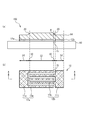
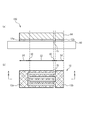
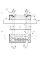
- FIG. 1A is a cross-sectional view of the resonator 100 according to the first embodiment
- FIG. 1B is a plan view of a part of the resonator 100
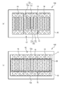
- FIG. 2A and FIG. 2B are plan views of the resonator 100 according to the first embodiment
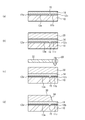
- FIG. 3A to FIG. 3D are cross-sectional views (part 1) showing a method of manufacturing the inclined region.
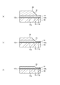
- FIG. 4A to FIG. 4C are cross-sectional views (No. 2) showing the method for manufacturing the inclined region.
- FIG. 5A is a cross-sectional view of the resonator 120 according to the first comparative example
- FIG. 5B is a plan view of a part of the resonator 120.
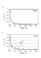
- FIG. 6B are diagrams showing conductance with respect to frequency of the resonators according to Example 1 and Comparative Example 1, respectively.
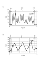
- FIG. 7A and FIG. 7B are diagrams showing the intensity of elastic waves of the resonators according to Example 1 and Comparative Example 1, respectively.
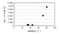
- FIG. 8 is a diagram illustrating the transverse mode spurious amount with respect to the inclination angle ⁇ in the first embodiment.
- FIG. 9A is a cross-sectional view of the resonator 122 according to the second comparative example, and FIG. 9B is a plan view of a part of the resonator 122.
- FIG. 10 is a diagram illustrating the conductance with respect to the frequency of the resonator according to the second comparative example.
- FIG. 10 is a diagram illustrating the conductance with respect to the frequency of the resonator according to the second comparative example.
- FIG. 11 is a diagram illustrating an example of conductance characteristics with respect to frequency.
- FIG. 12 is a diagram illustrating lateral mode spurious amounts with respect to inclination angles in different frequency ranges.
- FIG. 13A is a cross-sectional view of the resonator 102 according to the first modification of the first embodiment, and FIG. 13B is a plan view of a part of the resonator 102.
- FIG. 14A is a cross-sectional view of the resonator 104 according to the second modification of the first embodiment, and FIG. 14B is a plan view of a part of the resonator 104.
- FIG. 15A is a cross-sectional view of the resonator 106 according to the third modification of the first embodiment, and FIG.
- FIG. 15B is a plan view of a part of the resonator 106.
- FIG. 16A is a cross-sectional view of the resonator 108 according to the fourth modification of the first embodiment, and FIG. 16B is a plan view of a part of the resonator 108.
- FIG. 17 is a plan view of the resonator 110 according to the fifth modification of the first embodiment.
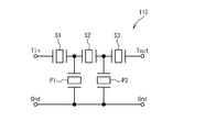
- FIG. 18 is a circuit diagram of the ladder filter 115 according to the second embodiment.
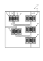
- FIG. 19 is a plan view of a ladder filter 115 according to the second embodiment.
- FIG. 20 is a diagram illustrating the measurement result of the pass characteristic of the ladder filter 115 according to the second embodiment.
- FIG. 21 is a block diagram of the module 70 according to the third embodiment.
- Example 1 is an example of a resonator as an elastic wave device.
- FIG. 1A is a cross-sectional view of the resonator 100 according to the first embodiment
- FIG. 1B is a plan view of a part of the resonator 100.
- FIG. 1A corresponds to the AA cross-sectional view of FIG.
- a dielectric film 14 such as a silicon oxide film is formed on a piezoelectric substrate 10 such as niobium lithium oxide or tantalum lithium oxide.
- Comb electrodes 12 a and 12 b made of a metal film such as Cu are formed between the substrate 10 and the dielectric film 14.
- Comb electrodes 12a and 12b are formed to face each other to form IDT 12.
- Comb electrodes 12a and 12b have electrode fingers 13a and 13b and bus bars 11a and 11b, respectively.
- the electrode fingers 13a and 13b extend in the same direction, and the electrode fingers 13a and 13b are alternately provided.
- a region where the electrode fingers 13 a and 13 b intersect is an intersecting region 52, and a region of the bus bars 11 a and 11 b is a bus bar region 54.
- the gap 15 there is an electrode gap 15 between the tip of one electrode finger 13a or 13b of the opposing comb electrodes 12a and 12b and the other comb electrode 12b of the opposing comb electrodes 12a and 12b.
- a region of the gap 15 is a gap region 50.
- the upper surface of the dielectric film 14 above the gap 15 is inclined with respect to the upper surface of the substrate 10 in the extending direction of the electrode fingers 13a and 13b.
- a region where the upper surface of the dielectric film 14 is inclined is an inclined region 20.
- the inclination angle ⁇ of the upper surface of the dielectric film 14 with respect to the upper surface of the substrate 10 is not less than 30 ° and not more than 50 °.
- the inclination angle of the inclined region 20 may not be constant.
- the inclination angle may be small near the periphery of the inclined region 20 and the inclination angle may be large near the center.
- the inclination angle ⁇ is an angle that is most inclined in the inclined region 20.
- FIG. 2A and FIG. 2B are plan views of the resonator 100 according to the first embodiment.
- FIG. 2A is a perspective view of the dielectric film 14.
- the reflectors 16 are provided on both sides of the IDT 12 in the direction intersecting the extending direction of the electrode fingers of the IDT 12.
- FIG. 2B is a diagram illustrating the dielectric film 14 and the inclined region 20. In FIG. 2B, the IDT 12 and the reflector 16 are illustrated by broken lines.
- an inclined region 20 is formed on the gap 15 of the IDT 12.
- the inclined region 20 is formed continuously from the IDT 12 to the reflector 16.
- the inclined region 20 is formed so as to surround the electrode finger of the IDT 12 and the electrode finger of the reflector.
- the resonator 100 functions as a resonator that resonates at a specific resonance frequency.
- the elastic wave propagating in the direction intersecting the electrode fingers 13a and 13b is a main mode elastic wave for functioning as a resonator.
- the transverse mode spurious is caused by an elastic wave propagating in the extending direction of the electrode fingers 13a and 13b. Therefore, the upper surface of the dielectric film 14 on the gap 15 is inclined.
- the elastic wave propagating in the extending direction of the electrode fingers 13a and 13b is dispersed. Therefore, transverse mode spurious can be suppressed.
- the bus bars 11 a and 11 b can be covered with the dielectric film 14. Therefore, unlike in Patent Document 2, a bus bar or the like is not exposed from the dielectric film 14. Therefore, deterioration of reliability can be suppressed.
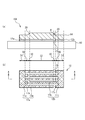
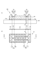
- FIG. 3A to FIG. 4C are cross-sectional views showing a method for manufacturing the inclined region 20.
- comb-shaped electrodes 12 a and 12 b are formed on the substrate 10.
- Dielectric film 14 is formed on substrate 10 so as to cover comb electrodes 12a and 12b.
- a photoresist 30 is applied on the dielectric film 14.
- the exposure mask 32 is used for the photoresist 30, and the photoresist 30 on the bus bar 11b is irradiated with ultraviolet rays UV.
- FIG. 3D by developing, the photoresist 30 on the bus bar 11b irradiated with ultraviolet rays is removed.
- the inclination of the end face 35 of the photoresist 30 is increased by post-baking.
- the photoresist 30 and the dielectric film 14 are dry-etched using an etching gas having a small selection ratio between the photoresist 30 and the dielectric film 14.
- the inclination of the end face 35 of the photoresist 30 is transferred to the dielectric film 14, and the inclined region 20 is formed on the gap 15.
- the photoresist 30 is removed.
- the inclined region 20 of the dielectric film 14 can be formed.
- the measured resonator 100 according to Example 1 is the resonator schematically shown in FIGS. 1 (a) to 2 (b).
- the substrate 10 mainly contains niobium lithium oxide.
- the comb electrodes 13a and 13b mainly contain Cu.
- the dielectric film 14 mainly contains silicon oxide.
- the film thickness of the dielectric film 14 on the electrode fingers 13a and 13b is about 0.3 ⁇ .
- the film thickness of the dielectric film 14 on the bus bars 11a and 11b is about 0.1 ⁇ .
- the inclination angle ⁇ is about 35 °.
- the length of the bottom side of the inclined region 20 is about 0.35 ⁇ .
- FIG. 5A is a cross-sectional view of the resonator 120 according to the first comparative example
- FIG. 5B is a plan view of a part of the resonator 120.
- FIG. 5A and 5B, the resonator 120 according to Comparative Example 1 is a dielectric on the gap 15 as compared with FIGS. 1A and 1B of Example 1.
- the upper surface of the film 14 is flat.
- Other configurations are the same as those of the resonator 100 according to the first embodiment, and the description thereof is omitted.
- FIG. 6A and FIG. 6B are diagrams showing conductance with respect to the frequency of the resonators according to Example 1 and Comparative Example 1, respectively.
- the frequency is near the anti-resonance frequency of the resonator.
- the conductance is relatively gentle with respect to the frequency.
- the resonator 120 according to the comparative example 1 has a frequency at which the conductance is maximized. This is due to transverse mode spurious.
- FIG. 7A and FIG. 7B are diagrams showing the intensity of elastic waves of the resonators according to Example 1 and Comparative Example 1, respectively.
- FIGS. 7A and 7B show the intensity of elastic waves in the extending direction of the electrode fingers 13a and 13b when a drive signal of 1910 MHz is applied to the IDT 12.
- FIG. The horizontal axis indicates the position Y in the extending direction of the electrode fingers 13a and 13b, and the vertical axis indicates the displacement amount I of the elastic wave.
- FIG. 7B in Comparative Example 1, a transverse mode elastic wave is excited in the intersecting region 52 between the bus bar regions 54.
- FIG. 7A in the first embodiment, a large number of higher order mode elastic waves are excited.
- FIG. 7B a specific strong high-order mode elastic wave is not excited.
- Example 1 the resonator 100 having inclination angles ⁇ of 80 °, 70 °, 45 °, 35 °, and 33 ° was manufactured, and the transverse mode spurious amount with respect to the inclination angle ⁇ was measured.
- FIG. 8 is a diagram illustrating the transverse mode spurious amount with respect to the inclination angle ⁇ in the first embodiment.
- the transverse mode spurious amount is, for example, the largest spurious spurious amount in the diagram of conductance with respect to the frequency as shown in FIGS. 6 (a) and 6 (b). As shown in FIG. 8, the transverse mode spurious amount increases as the inclination angle ⁇ increases. As the inclination angle ⁇ decreases, the transverse mode spurious amount decreases.
- FIG. 9A is a cross-sectional view of the resonator 122 according to Comparative Example 2
- FIG. 9B is a plan view of a part of the resonator 122.
- the resonator 122 according to the second comparative example has the inclined region 20 in the bus bar region. 54, the upper surface of the dielectric film 14 on the gap 15 is flat.
- Other configurations are the same as those of the resonator 100 according to the first embodiment, and the description thereof is omitted.
- FIG. 10 is a diagram showing the conductance with respect to the frequency of the resonator according to Comparative Example 2. As shown in FIG. 10, although the spurious is smaller than that in the first comparative example, a larger transverse mode spurious is observed than in the first embodiment. As described above, the transverse mode spurious can be suppressed by forming the inclined region 20 on the gap 15.
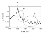
- FIG. 11 is a diagram showing an example of conductance characteristics with respect to frequency.
- FIG. 11 is an example showing the relationship between the frequency and the conductance, and the resonance frequency and the like do not match those of Comparative Example 1 and Example 1 shown in FIGS. 6 (a) and 6 (b).
- the resonance frequency fr is around 1750 MHz
- the anti-resonance frequency is around 1810 MHz.
- the transverse mode spurious is classified into a transverse mode spurious in the frequency range 40 between the resonance frequency and the antiresonant frequency and a transverse mode spurious in the frequency range 42 near the antiresonant frequency.
- the transverse mode spurious amount with respect to the inclination angle ⁇ was measured.
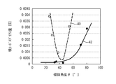
- FIG. 12 is a diagram showing transverse mode spurious amounts with respect to inclination angles in different frequency ranges.
- a black circle is a measurement result in the frequency range 42, and a solid line is an approximate curve of the black circle.
- a white circle is a measurement result of the frequency range 40, and a broken line is an approximate curve of a white circle.
- the measurement points in the frequency range 42 are the same as in FIG.
- the amount of transverse mode spurious in the frequency range 42 was measured when the inclination angle ⁇ was about 24 °, 28 °, 38 °, and 55 °. When the inclination angle ⁇ is 38 °, the transverse mode spurious is the smallest.
- the transverse mode spurious amount becomes a minimum value when the inclination angle ⁇ is around 40 ° to 45 °.
- the inclination angle ⁇ is preferably 45 ° or less as shown in FIG.
- the optimum inclination angle ⁇ is different from the frequency range 42. From FIG. 12, in order to make the transverse mode spurious amount 0.0025 S or less in the vicinity of the frequency range 40, the inclination angle ⁇ is preferably 30 ° or more and 50 ° or less.
- the elastic wave is more preferably 32 ° or more and 48 ° or less, and more preferably 35 ° or more and 45 ° or less.
- the characteristics of the elastic wave can be generalized by normalizing with the wavelength ⁇ of the elastic wave. For this reason, the inclination angle ⁇ does not depend on ⁇ . Therefore, about FIG. 12, it can generalize also about the resonator which has a different resonant frequency.
- the upper surface of the dielectric film 14 above the gap 15 is inclined with respect to the upper surface of the substrate 10 in the extending direction of the electrode fingers 13 a and 13 b, and the dielectric film 14 with respect to the upper surface of the substrate 10.
- the upper surface has an inclination angle of 30 ° or more and 50 ° or less.
- a resonator whose crossing region is constant in the main elastic wave propagation direction is called a normal electrode.
- a weighting In order to suppress the transverse mode spurious, it is also conceivable to weight the intersecting area by a weighting. In the first embodiment, the transverse mode spurious can be suppressed, and thus it is not necessary to weight the abodies.
- the inclined region 20 can be provided in the gap region 50 as in the first embodiment in the resonator subjected to the weighting.
- the inclined region 20 may include at least a part of the gap region 50, but the upper surface of the dielectric film 14 extends over the entire upper portion of the gap 15 as shown in FIGS. 1A and 1B of the first embodiment. It is preferable to be inclined. Thereby, transverse mode spurious can be suppressed more. Further, the inclined region 20 may include a part of the intersection region 52 and the bus bar region 54.
- the film thickness of the dielectric film 14 on the electrode fingers 13a and 13b is different from the film thickness of the dielectric film 14 on the bus bars 11a and 11b.
- the slope of the dielectric film 14 can be provided on the gap 15 without exposing the surface of the bus bar 11 from the dielectric film 14.
- the film thickness difference of the dielectric film 14 caused by the inclination of the upper surface of the dielectric film 14 is larger than the film thicknesses of the opposing comb electrodes 12a and 12b.
- FIG. 13A is a cross-sectional view of the resonator 102 according to the first modification of the first embodiment
- FIG. 13B is a plan view of a part of the resonator 102.
- the resonator 102 according to the first modification of the first embodiment is compared with the first embodiment shown in FIG. 1A and FIG.
- the dielectric film 14 of 54 is thicker than the dielectric film 14 of the intersection region 52.
- Other configurations are the same as those of the resonator 100 according to the first embodiment, and the description thereof is omitted.
- the dielectric film 14 in the bus bar region 54 may be thinner than the dielectric film 14 in the intersecting region 52 as in the first embodiment, but may be reversed as in the first modification of the first embodiment.
- FIG. 14A is a cross-sectional view of the resonator 104 according to the second modification of the first embodiment
- FIG. 14B is a plan view of a part of the resonator 104.
- the resonator 104 according to the second modification of the first embodiment includes an electrode finger.
- Opposing comb electrodes 12b and 12a and dummy electrode fingers 17b and 17a are provided in the extending direction of the tips of 13a and 13b, respectively.
- Dummy electrode fingers 17a and 17b are connected to bus bars 11a and 11b, respectively.
- the region of the dummy electrode fingers 17a and 17b is a dummy region 56.
- the inclined region 20 is formed in the gap region 50.
- Other configurations are the same as those in FIG. 1A and FIG. 1B of the first embodiment, and a description thereof will be omitted.
- the resonator 104 may be provided with dummy electrode fingers 17a and 17b.
- the inclined region 20 may include a part of the intersecting region 52, the bus bar region 54, and the dummy region 56.
- FIG. 15A is a cross-sectional view of the resonator 106 according to the third modification of the first embodiment
- FIG. 15B is a plan view of a part of the resonator 106.
- the resonator 106 according to the third modification of the first embodiment includes an inclined region as compared with FIGS. 1A and 1B of the first embodiment.
- 20 includes a first inclined region 20a and a second inclined region 20b.
- the first inclined region 20a is inclined so that the upper surface of the dielectric film 14 is lowered from the intersecting region 52 side to the bus bar region 54 side.
- the second inclined region 20b is inclined so that the upper surface of the dielectric film 14 becomes higher from the intersecting region 52 side to the bus bar region 54 side.
- the first inclined region 20a is provided on the crossing region 52 side of the gap region 50, and the second inclined region 20b is provided on the bus bar region 54 side of the gap region 50. Further, the inclined region 20 is not provided on the bus bar region 54 side of the inclined region 20.
- the inclined region 20 may include a first inclined region 20a and a second inclined region 20b. Further, the inclined region 20 may be formed in a part of the gap region 50.
- the inclination angle ⁇ a of the first inclined region 20a and the inclination angle ⁇ b of the second inclined region 20b may be the same or different. At least one of the inclination angles ⁇ a and ⁇ b is preferably 30 ° or more and 50 ° or less. It is more preferable that both the inclination angles ⁇ a and ⁇ b are 30 ° or more and 50 ° or less. Furthermore, in order to scatter elastic waves propagating in the extending direction of the electrode fingers 13a and 13b, the inclination angle ⁇ a is preferably 30 ° or more and 50 ° or less.
- FIG. 16A is a cross-sectional view of the resonator 108 according to the fourth modification of the first embodiment
- FIG. 16B is a plan view of a part of the resonator 108.
- the fourth modification is different from the second modification of the third embodiment in FIGS. 15A and 15B in the third modification of the first embodiment.
- Another dielectric film 14 a is formed on the dielectric film 14 in the inclined region 20 b and the bus bar region 54.
- the dielectric film 14a is, for example, a silicon oxide film.
- Other configurations are the same as those of FIG. 15A and FIG. 15B of the third modification of the first embodiment, and a description thereof will be omitted.
- the dielectric film 14 may be thick in a part of the gap region 50.
- FIG. 17 is a plan view of the resonator 110 according to the fifth modification of the first embodiment.
- the inclined region 20 is provided between the gap region 50 of the IDT 12 and the IDT 12 and the reflector 16.
- Other configurations are the same as those of the resonator 100 according to the first embodiment, and the description thereof is omitted.
- region 20 should just be provided in the gap area
- the inclined region 20 may be provided only in the gap region 50 of the IDT 12.
- the substrate 10 is a piezoelectric body
- the dielectric film 14 may be a piezoelectric body.
- Example 2 is an example in which the acoustic wave device is a filter.
- FIG. 18 is a circuit diagram of the ladder filter 115 according to the second embodiment. As shown in FIG. 18, series resonators S1 to S3 are connected in series between the input terminal Tin and the output terminal Tout. Parallel resonators P1 and P2 are connected in parallel between the input terminal Tin and the output terminal Tout. One end of each of the parallel resonators P1 and P2 is connected to the ground Gnd.
- FIG. 19 is a plan view of the ladder type filter 115 according to the second embodiment.
- Series resonators S1 to S3 and parallel resonators P1 and P2 are formed on the piezoelectric substrate 10.
- the series resonators S1 to S3 and the parallel resonators P1 and P2 are resonators according to the first embodiment or its modification.
- Each resonator is electrically connected by a wiring 22.
- Each resonator has an IDT 12 and a reflector 16 sandwiching the IDT 12.
- FIG. 20 is a diagram illustrating the measurement results of the pass characteristics of the ladder filter 115 according to the second embodiment.
- Each resonator of the ladder type filter 115 of the second embodiment has the same structure as the resonator 100 of the first embodiment in which FIG. 6A is measured, and the inclination angle ⁇ is 35 °.
- Each resonator of the ladder type filter of the comparative example 3 has the same structure as the resonator 120 of the comparative example 1 in which FIG. 6B is measured.
- the ripple caused by the transverse mode spurious in the pass band is smaller in the second embodiment than in the third comparative example.
- a filter can be formed using the first embodiment and its modifications.
- the second embodiment is an example of a ladder type filter, the first embodiment or a modification thereof may be used for a multimode filter. Thereby, the ripple in a pass band can be suppressed.
- the vicinity of the resonance frequency of the series resonators S1 to S3 is a pass band.
- the vicinity of the antiresonance frequency of the parallel resonators P1 and P2 is a pass band. Therefore, the inclination angle ⁇ of the series resonators S1 to S3 is set in a range of 30 ° to 50 ° (for example, 45 °). Thereby, as shown in FIG. 12, the transverse mode spurious between the resonance frequency and the anti-resonance frequency can be suppressed.
- the inclination angle ⁇ of the parallel resonators P1 and P2 is set to be smaller than 45 °.
- transverse mode spurious near the antiresonance frequency of the parallel resonators P1 and P2 can be suppressed.
- the inclination angle ⁇ of the parallel resonators P1 and P2 to 30 °, it is possible to suppress the transverse mode spurious near the antiresonance frequency of the parallel resonators P1 and P2 with a margin regardless of the variation in angle. Therefore, it is possible to further suppress the passband ripple.
- the inclination angles ⁇ of the plurality of IDTs 12 can be varied.
- a resonator that wants to suppress transverse mode spurious between the resonance frequency and the anti-resonance frequency has an inclination angle ⁇ of 30 ° to 50 °.
- the angle is 35 ° to 45 °.
- a resonator that wants to suppress transverse mode spurious near the anti-resonance frequency has an inclination angle ⁇ of 45 ° or less.
- it is 35 degrees or less, More preferably, it shall be 30 degrees or less.
- the inclination angle ⁇ can be made different between the first IDT included in the series resonators S1 to S3 and the second IDT included in the parallel resonators P1 and P2.
- the resonator according to each modification of the first embodiment can be used.
- Example 3 is an example of an RF (Radio-Frequency) module.
- FIG. 21 is a block diagram of the module 70 according to the third embodiment. As shown in FIG. 21, the module 70 mainly includes a duplexer 73, a power amplifier 74, a transmission filter 75, a low noise amplifier 76, and a reception filter 77.
- the duplexer 73 includes filters 71 and 72. A transmission signal is input to the transmission terminal Ttx.
- the transmission filter 75 filters the transmission signal.
- the power amplifier 74 amplifies the transmission signal.
- the filter 71 of the duplexer 73 filters the transmission signal and outputs the transmission signal to the antenna terminal Tant.
- the filter 72 of the duplexer 73 suppresses the transmission signal from leaking to the low noise amplifier 76 side.
- a reception signal is input to the antenna terminal Tant.
- the filter 72 of the duplexer 73 outputs the received signal to the low noise amplifier 76.
- the filter 71 of the duplexer 73 suppresses the reception signal from leaking to the power amplifier 74 side.
- the low noise amplifier 76 amplifies the received signal.
- the reception filter 77 filters the reception signal and outputs it to the reception terminal Trx.
- the filters 71, 72, 75, and 77 can be the filter of the second embodiment.
- the module 70 according to the third embodiment can be used as an RF module for mobile communication such as a mobile phone.
- the resonator according to the first embodiment or a modification thereof can be used for the module.
Landscapes
- Physics & Mathematics (AREA)
- Acoustics & Sound (AREA)
- Engineering & Computer Science (AREA)
- Manufacturing & Machinery (AREA)
- Surface Acoustic Wave Elements And Circuit Networks Thereof (AREA)
Abstract
基板10と、前記基板上に形成された誘電体膜14と、前記基板と前記誘電体膜との間に設けられ、それぞれ電極指13を含み対向する櫛型電極12と、を備え、前記基板および誘電体膜の少なくとも一方は圧電体であり、前記対向する櫛型電極のうち一方の電極指の先端と、前記対向する櫛型電極のうち他方の櫛型電極の間のギャップ15の上方の前記誘電体膜の上面は、前記電極指の延伸方向に、前記基板の上面に対し傾斜しており、前記基板の上面に対する前記誘電体膜の上面の傾斜角度は30°以上かつ50°以下である弾性波デバイス。
Description
本発明は、弾性波デバイスおよびモジュールに関し、例えば櫛型電極を有する弾性波デバイスおよびモジュールに関する。
弾性波デバイスは、例えば無線機器等のフィルタ素子や発振子として用いられている。弾性波を応用したデバイスとして弾性表面波(SAW:Surface Acoustic Device)デバイスが知られている。SAWデバイスは、例えば45MHz~2GHzの周波数における無線信号を処理する各種回路、例えば送信バンドパスフィルタ、受信バンドパスフィルタ、局所発振器用フィルタ、アンテナ共用器、IF(Intermediate frequency)フィルタおよびFM(Frequency Modulation)変調器等に用いられる。
SAWデバイスは、2つの対向した櫛型電極を備えるIDT(Interdigital Transducer)を有している。櫛型電極は、バスバーとバスバーから同じ方向に延伸し弾性波を励振する電極指とを有している。対向する櫛型電極の電極指は互い違いに配置される。弾性波は電極指の延伸方向に交差する方向に伝搬する。しかしながら、電極指方向に伝播する弾性波に起因する横モードスプリアスが発生する。櫛型電極の電極指の先端に、ギャップを介し他方の櫛型電極のダミー電極を設け、ダミー電極とダミー電極が隣り合う交差電極のダミー部の長さとを異ならせることにより、横モードの弾性波を散乱させ、スプリアスを抑える方法が検討されている(例えば、特許文献1)。電極指上に誘電体膜を形成し、バスバー上に誘電体膜を形成しないことによりスプリアスを抑制する方法が知られている(例えば、特許文献2)。
誘電体膜を基板上に形成した弾性波デバイスでは、励振される弾性波は誘電体膜まで分布している。このため、特許文献1の方法では、基板と誘電膜との界面の横モードの弾性波の一部を散乱させる。しかし、誘電体膜内の弾性波を散乱させることは難しい。よって、スプリアスの抑制は十分ではない。また、特許文献2の方法を用いると、バスバー等の表面が誘電体膜から露出する。これにより、信頼性が低下する可能性がある。
本発明は、上記課題に鑑みなされたものであり、スプリアスの抑制を目的とする。
本発明は、基板と、前記基板上に形成された誘電体膜と、前記基板と前記誘電体膜との間に設けられ、それぞれ電極指を含み対向する櫛型電極と、を備え、前記基板および誘電体膜の少なくとも一方は圧電体であり、前記対向する櫛型電極のうち一方の電極指の先端と、前記対向する櫛型電極のうち他方の櫛型電極の間のギャップの上方の前記誘電体膜の上面は、前記電極指の延伸方向に、前記基板の上面に対し傾斜しており、前記基板の上面に対する前記誘電体膜の上面の傾斜角度は30°以上かつ50°以下であることを特徴とする弾性波デバイスである。本発明によれば、スプリアスを抑制することができる。
上記構成において、前記誘電体膜の上面は、前記ギャップの上方全体にわたり傾斜している構成とすることができる。
上記構成において、前記対向する櫛型電極は、それぞれ前記電極指とバスバーとを含み、前記電極指上の前記誘電体膜の膜厚と、前記バスバー上の前記誘電体膜の膜厚とは異なる構成とすることができる。
上記構成において、前記誘電体膜の上面の傾斜により生じる前記誘電体膜の膜厚差は、前記対向する櫛型電極の膜厚より大きい構成とすることができる。
上記構成において、前記対向する櫛型電極を含むIDTを複数有し、前記複数のIDTは前記傾斜角度が異なる構成とすることができる。
上記構成において、前記複数のIDTは、ラダー型フィルタの直列共振器に含まれる第1IDTと並列共振器の含まれる第2IDTとを含み、前記第1IDTと前記第2IDTとで、前記傾斜角度が異なる構成とすることができる。
本発明は、上記弾性波デバイスを含むことを特徴とするモジュールである。
本発明によれば、スプリアスを抑制することができる。
以下、図面を参照し、本発明の実施例について説明する。
実施例1は、弾性波デバイスとして共振器の例である。図1(a)は、実施例1に係る共振器100の断面図、図1(b)は、共振器100の一部の平面図である。図1(a)は、図1(b)のA-A断面図に対応する。図1(a)および図1(b)のように、例えばリチウム酸ニオブまたはリチウム酸タンタル等の圧電性の基板10上に酸化シリコン膜等の誘電体膜14が形成されている。基板10と誘電体膜14との間にCu等の金属膜からなる櫛型電極12aおよび12bが形成されている。櫛型電極12aおよび12bは対向して形成され、IDT12を形成している。櫛型電極12aおよび12bはそれぞれ、電極指13aおよび13bとバスバー11aおよび11bを有している。電極指13aおよび13bは同じ方向に延伸しており、電極指13aと13bとが交互に設けられている。電極指13aと13bとが交差する領域が交差領域52であり、バスバー11aおよび11bの領域がバスバー領域54である。
対向する櫛型電極12aおよび12bのうち一方の電極指13aまたは13bの先端と、対向する櫛型電極12aおよび12bのうち他方の櫛型電極12bと間に電極のギャップ15が存在する。このギャップ15の領域がギャップ領域50である。ギャップ15の上方の誘電体膜14の上面は、電極指13aおよび13bの延伸方向に、基板10の上面に対し傾斜している。誘電体膜14の上面が傾斜している領域が傾斜領域20である。傾斜領域20における、基板10の上面に対する誘電体膜14の上面の傾斜角度θは30°以上かつ50°以下である。なお、傾斜領域20の傾斜角度は一定でなくともよく、例えば、傾斜領域20の周辺付近では、傾斜角度が小さく、中心付近では、傾斜角度が大きくてもよい。この場合、傾斜角度θは、傾斜領域20において最も傾斜している角度である。
図2(a)および図2(b)は実施例1に係る共振器100の平面図である。図2(a)は、誘電体膜14を透視した図である。図2(a)のように、IDT12に対し、IDT12の電極指の延伸方向に交差する方向の両側に反射器16が設けられている。図2(b)は、誘電体膜14および傾斜領域20を図示した図である、図2(b)において、IDT12および反射器16は破線で図示している。図2(b)のように、IDT12のギャップ15上に傾斜領域20が形成されている。傾斜領域20は、IDT12から反射器16に連続して形成されている。傾斜領域20は、IDT12の電極指および反射器の電極指を囲むように形成されている。
特定の周波数を有する高周波信号がIDT12に印加されることにより、IDT12の電極指13aおよび13bにより基板10および誘電体膜14内に弾性波が励振される。励振された弾性波は、電極指13aおよび13bに直交する方向に伝搬する。弾性波は反射器16により反射される。これにより、共振器100は特定の共振周波数において共振する共振器として機能する。電極指13aおよび13bに交差する方向に伝搬する弾性波は、共振器として機能するための主モードの弾性波である。横モードスプリアスは、電極指13aおよび13bの延伸方向に伝搬する弾性波に起因する。そこで、ギャップ15上の誘電体膜14の上面を斜めとする。これにより、電極指13aおよび13bの延伸方向に伝搬する弾性波が分散する。よって、横モードスプリアスを抑制できる。さらに、バスバー11aおよび11bを誘電体膜14で覆うことができる。このため、特許文献2のように、バスバー等が誘電体膜14から露出することがない。よって、信頼性の劣化を抑制することができる。
次に、誘電体膜14の傾斜領域20の形成方法について説明する。図3(a)から図4(c)は、傾斜領域20の作製方法を示す断面図である。図3(a)のように、基板10上に櫛型電極12aおよび12bを形成する。櫛型電極12aおよび12bを覆うように基板10上に誘電体膜14を形成する。図3(b)のように、誘電体膜14上にフォトレジスト30を塗布する。図3(c)のように、フォトレジスト30に露光マスク32を用い、バスバー11b上のフォトレジスト30に紫外線UVを照射する。図3(d)のように、現像することにより、紫外線が照射されたバスバー11b上のフォトレジスト30が除去される。
図4(a)のように、ポストベークすることにより、フォトレジスト30の端面35の傾斜が大きくなる。図4(b)のように、フォトレジスト30と誘電体膜14との選択比の小さいエッチングガスを用い、フォトレジスト30と誘電体膜14とをドライエッチングする。これにより、誘電体膜14にフォトレジスト30の端面35の傾斜が転写され、ギャップ15上に傾斜領域20が形成される。図4(c)のように、フォトレジスト30を除去する。以上により、誘電体膜14の傾斜領域20を形成することができる。
次に、比較例1に係る共振器と実施例1に係る共振器の櫛型電極12aおよび12b間の高周波数信号におけるコンダクタンスを測定し、比較した。測定した実施例1に係る共振器100は、図1(a)から図2(b)に概略を示した共振器である。基板10はリチウム酸ニオブを主に含む。櫛型電極13aおよび13bはCuを主に含む。誘電体膜14は酸化シリコンを主に含む。弾性波デバイスとして機能するための弾性波の波長をλとしたとき、電極指13aおよび13bの長さはそれぞれ約30λである。ギャップ15の長さは約0.25λである。電極指13aおよび13b上の誘電体膜14の膜厚は約0.3λである。バスバー11aおよび11b上の誘電体膜14の膜厚は約0.1λである。傾斜角度θは約35°である。傾斜領域20の底辺の長さは約0.35λである。
図5(a)は、比較例1に係る共振器120の断面図、図5(b)は、共振器120の一部の平面図である。図5(a)および図5(b)を参照し、実施例1の図1(a)および図1(b)と比較し、比較例1に係る共振器120は、ギャップ15上の誘電体膜14の上面が平坦である。その他の構成は実施例1に係る共振器100と同じであり説明を省略する。
図6(a)および図6(b)は、それぞれ実施例1および比較例1に係る共振器の周波数に対するコンダクタンスを示す図である。周波数は、共振器の反共振周波数付近である。図6(a)のように、実施例1に係る共振器100においては、周波数に対しコンダクタンスは比較的なだらかである。一方、図6(b)のように、比較例1に係る共振器120においては、コンダクタンスが極大となる周波数がある。これは、横モードのスプリアスに起因する。
次に、電極指の延伸方向の弾性波の分布を測定した。図7(a)および図7(b)は、それぞれ実施例1および比較例1に係る共振器の弾性波の強度を示す図である。図7(a)および図7(b)は、IDT12に1910MHzの駆動信号を印加した場合の、電極指13aおよび13bの延伸方向の弾性波の強度を示している。横軸は、電極指13aおよび13bの延伸方向の位置Yを示し、縦軸は、弾性波の変位量Iを示している。図7(b)のように、比較例1では、バスバー領域54間の交差領域52において、横モードの3次モードの弾性波が励振されている。一方、図7(a)のように、実施例1では、多数の高次モードの弾性波が励振されている。この結果、図7(b)のように、特定の強い高次モードの弾性波は励振されていない。
次に、実施例1において、傾斜角度θが80°、70°、45°、35°および33°の共振器100を作製し、傾斜角度θに対する横モードスプリアス量を測定した。図8は、実施例1における傾斜角度θに対する横モードスプリアス量を示す図である。横モードスプリアス量は、例えば、図6(a)および図6(b)のような周波数に対するコンダクタンスの図中、最も大きいスプリアスのスプリアス量である。図8のように、横モードスプリアス量は、傾斜角度θが大きいと大きくなる。傾斜角度θが小さくなるにしたがい、横モードスプリアス量は小さくなる。特に、傾斜角度θが45°以下になると、横モードスプリアスはほとんど観測されない。これは、傾斜角度θが大きくなると、傾斜領域20の幅が狭くなり、ギャップ領域50に占める傾斜領域20の幅が小さくなるためである。
図9(a)は、比較例2に係る共振器122の断面図、図9(b)は、共振器122の一部の平面図である。実施例1の図1(a)および図1(b)と比較し、図9(a)および図9(b)のように、比較例2に係る共振器122は、傾斜領域20がバスバー領域54に位置し、ギャップ15上の誘電体膜14の上面は平坦である。その他の構成は実施例1に係る共振器100と同じであり説明を省略する。
図10は、比較例2に係る共振器の周波数に対するコンダクタンスを示す図である。図10のように、比較例1に比べスプリアスは小さいものの、実施例1に比べると大きな横モードスプリアスが観測される。以上のように、ギャップ15上に傾斜領域20を形成すことにより、横モードスプリアスを抑制できる。
図11は、周波数に対するコンダクタンスの特性の例を示す図である。図11は、周波数とコンダクタンスとの関係を示す一例であり、図6(a)および図6(b)に示した比較例1および実施例1と共振周波数等は一致していない。図11の例では、共振周波数frは1750MHz付近であり、反共振周波数は1810MHz付近である。ここで、横モードスプリアスを、共振周波数と反共振周波数との間の周波数範囲40の横モードスプリアスと、反共振周波数付近の周波数範囲42の横モードスプリアスに分類した。周波数範囲42に加え、周波数範囲40においても、傾斜角度θに対する横モードスプリアス量を測定した。
図12は、異なる周波数範囲の傾斜角度に対する横モードスプリアス量を示す図である。図12において、黒丸は、周波数範囲42の測定結果であり、実線は、黒丸の近似曲線である。白丸は、周波数範囲40の測定結果であり、破線は、白丸の近似曲線である。周波数範囲42の測定点は図8と同じである。周波数範囲42の横モードスプリアス量は、傾斜角度θが約24°、28°、38°および55°について測定した。傾斜角度θが38°のとき、横モードスプリアスが最も小さくなっている。近似曲線では、傾斜角度θが40°~45°付近において横モードスプリアス量は極小値となる。以上のように、周波数範囲42付近の横モードスプリアスを問題にする場合、図8のように、傾斜角度θが45°以下であることが好ましい。一方、周波数範囲40付近の横モードスプリアスを問題にする場合は、最適な傾斜角度θが周波数範囲42とは異なる。図12より、周波数範囲40付近において、横モードスプリアス量を0.0025S以下とするためには、傾斜角度θは30°以上かつ50°以下が好ましい。さらに、32°以上かつ48°以下がより好ましく、35°以上かつ45°以下がより好ましい。なお、弾性波の特性は弾性波の波長λで規格化することにより、一般化することが可能である。このため、傾斜角度θは、λに対し依存しない。よって、図12については、異なる共振周波数を有する共振器についても一般化することができる。
実施例1によれば、ギャップ15の上方の誘電体膜14の上面は、電極指13aおよび13bの延伸方向に、基板10の上面に対し傾斜しており、基板10の上面に対する誘電体膜14の上面の傾斜角度は30°以上かつ50°以下である。これにより、特に、共振周波数と反共振周波数との間の周波数範囲40の横モードスプリアスを抑制することができる。さらに、バスバー11aおよび11bを誘電体膜14で覆うことができるため、信頼性の劣化を抑制できる。
実施例1のように、交差領域が主な弾性波の伝搬方向に一定である共振器は正規型電極とよばれる。横モードスプリアスを抑制するため、交差領域に重み付けするアボダイズ重み付けすることも考えられる。実施例1においては、横モードスプリアスを抑制できるため、アボダイズ重み付けしなくてもよい。また、さらに横モードスプリアスを抑制するため、アボダイズ重み付けした共振器に実施例1のように、ギャップ領域50に傾斜領域20を設けることもできる。
傾斜領域20はギャップ領域50の少なくとも一部を含めばよいが、実施例1の図1(a)および図1(b)のように、誘電体膜14の上面は、ギャップ15の上方全体にわたり傾斜していることが好ましい。これにより、より横モードスプリアスを抑制することができる。また、傾斜領域20は、交差領域52およびバスバー領域54の一部を含んでもよい。
さらに、電極指13aおよび13b上の誘電体膜14の膜厚と、バスバー11aおよび11b上の誘電体膜14の膜厚とは異なる。これにより、バスバー11の表面を誘電体膜14から露出させることなく、ギャップ15上に誘電体膜14の傾斜を設けることができる。
さらに、誘電体膜14の上面の傾斜により生じる誘電体膜14の膜厚差は、対向する櫛型電極12aおよび12bの膜厚より大きい。これにより、傾斜領域20において、横モードの弾性波をより反射することができる。よって、横モードスプリアスをより抑制することができる。
次に、実施例1の変形例1について説明する。図13(a)は、実施例1の変形例1に係る共振器102の断面図、図13(b)は、共振器102の一部の平面図である。図13(a)および図13(b)のように、実施例1の図1(a)および図1(b)と比較し、実施例1の変形例1に係る共振器102は、バスバー領域54の誘電体膜14が交差領域52の誘電体膜14より厚い。その他の構成は実施例1に係る共振器100と同じであり説明を省略する。実施例1のように、バスバー領域54の誘電体膜14が交差領域52の誘電体膜14より薄くてもよいが、実施例1の変形例1のように、逆でもよい。
次に、実施例1の変形例2について説明する。図14(a)は、実施例1の変形例2に係る共振器104の断面図、図14(b)は、共振器104の一部の平面図である。図14(a)および図14(b)のように、実施例1の図1(a)および図1(b)と比較し、実施例1の変形例2に係る共振器104は、電極指13aおよび13bの先端の延伸方向に、それぞれ対向する櫛型電極12bおよび12aのダミー電極指17bおよび17aが設けられている。ダミー電極指17aおよび17bは、それぞれバスバー11aおよび11bに接続されている。ダミー電極指17aおよび17bの領域がダミー領域56である。傾斜領域20は、ギャップ領域50に形成されている。その他の構成は、実施例1の図1(a)および図1(b)と同じであり説明を省略する。実施例1の変形例2のように、共振器104にダミー電極指17aおよび17bが設けられていてもよい。なお、傾斜領域20は、交差領域52、バスバー領域54およびダミー領域56の一部を含んでもよい。なお、実施例1の変形例1、3、4または5にダミー電極を設けてもよい。
次に、実施例1の変形例3について説明する。図15(a)は、実施例1の変形例3に係る共振器106の断面図、図15(b)は、共振器106の一部の平面図である。図15(a)および図15(b)のように、実施例1の図1(a)および図1(b)と比較し、実施例1の変形例3に係る共振器106は、傾斜領域20が、第1傾斜領域20aと第2傾斜領域20bを含む。第1傾斜領域20aは、交差領域52側からバスバー領域54側に誘電体膜14の上面が低くなるように傾斜する。第2傾斜領域20bは、交差領域52側からバスバー領域54側に誘電体膜14の上面が高くなるように傾斜する。第1傾斜領域20aがギャップ領域50の交差領域52側に設けられ、第2傾斜領域20bがギャップ領域50のバスバー領域54側に設けられている。さらに、傾斜領域20のバスバー領域54側には傾斜領域20が設けられていない。その他の構成は、実施例1の図1(a)および図1(b)と同じであり説明を省略する。実施例1の変形例3のように、傾斜領域20は、第1傾斜領域20aと第2傾斜領域20bを含んでもよい。また、傾斜領域20は、ギャップ領域50の一部に形成されていてもよい。さらに、第1傾斜領域20aの傾斜角度θaと第2傾斜領域20bの傾斜角度θbは、同じでもよいが、異なっていてもよい。傾斜角度θaおよびθbの少なくとも一方は、30°以上かつ50°以下が好ましい。傾斜角度θaおよびθbの両方が30°以上かつ50°以下であることがより好ましい。さらに、電極指13aおよび13bの延伸方向に伝搬する弾性波を散乱させるためには、傾斜角度θaが30°以上かつ50°以下であることが好ましい。
次に、実施例1の変形例4について説明する。図16(a)は、実施例1の変形例4に係る共振器108の断面図、図16(b)は、共振器108の一部の平面図である。変形例4は、図16(a)および図16(b)のように、実施例1の変形例3の図15(a)および図15(b)と比較して、共振器108の第2傾斜領域20bおよびバスバー領域54の誘電体膜14上に、別の誘電体膜14aが形成されている。誘電体膜14aは、例えば酸化シリコン膜である。その他の構成は、実施例1の変形例3の図15(a)および図15(b)と同じであり説明を省略する。実施例1の変形例4のように、ギャップ領域50の一部は誘電体膜14の膜厚が厚くなっていてもよい。
次に、実施例1の変形例5について説明する。図17は、実施例1の変形例5に係る共振器110の平面図である。図17のように、傾斜領域20が、IDT12のギャップ領域50と、IDT12と反射器16との間に設けられている。その他の構成は実施例1に係る共振器100と同じであり説明を省略する。実施例1の変形例5のように、傾斜領域20は、IDT12aおよび12bのギャップ領域50に設けられていればよい。例えば、傾斜領域20は、IDT12のギャップ領域50のみに設けられていればよい。
なお、実施例1およびその変形例において、基板10が圧電体である例を説明したが、基板10および誘電体膜14の少なくとも一方が圧電体であればよい。
実施例2は、弾性波デバイスがフィルタの例である。図18は、実施例2に係るラダー型フィルタ115の回路図である。図18のように、入力端子Tinと出力端子Toutとの間に直列共振器S1からS3が直列に接続されている。入力端子Tinと出力端子Toutとの間に並列共振器P1およびP2が並列に接続されている。並列共振器P1およびP2それぞれの一端はグランドGndに接続されている。
図19は、実施例2に係るラダー型フィルタ115の平面図である。圧電性の基板10に直列共振器S1からS3並びに並列共振器P1およびP2が形成されている。直列共振器S1からS3並びに並列共振器P1およびP2は、実施例1またはその変形例に係る共振器である。各共振器間は配線22により電気的に接続されている。各共振器は、IDT12とIDT12を挟む反射器16とを有している。
図20は、実施例2に係るラダー型フィルタ115の通過特性の測定結果を示す図である。実施例2のラダー型フィルタ115の各共振器は、図6(a)を測定した実施例1の共振器100と同じ構造であり、傾斜角度θは、35°である。比較例3のラダー型フィルタの各共振器は、図6(b)を測定した比較例1の共振器120と同じ構造である。図20のように、実施例2においては、比較例3に対し、通過帯域内の横モードスプリアスに起因したリップルが小さくなっている。
実施例2のように、実施例1およびその変形例を用いフィルタを形成することができる。実施例2は、ラダー型フィルタの例であったが、多重モードフィルタに実施例1またはその変形例を用いることもできる。これにより、通過帯域内のリップルを抑制することができる。
また、ラダー型フィルタにおいては、直列共振器S1~S3の共振周波数付近が通過帯域となる。一方、並列共振器P1およびP2の反共振周波数付近が通過帯域となる。よって、直列共振器S1~S3の傾斜角度θを30°~50°の範囲(例えば45°)とする。これにより、図12のように、共振周波数と反共振周波数の間の横モードスプリアスを抑制できる。一方、並列共振器P1およびP2の傾斜角度θは45°より小さくする。これにより、並列共振器P1およびP2の反共振周波数付近の横モードスプリアスを抑制できる。例えば、並列共振器P1およびP2の傾斜角度θを30°とすることにより、角度のばらつきによらず余裕を持って、並列共振器P1およびP2の反共振周波数付近の横モードスプリアスを抑制できる。よって、通過帯域のリップルをより抑制することができる。
以上のように、IDT12を複数有する弾性波デバイスにおいて、複数のIDT12の傾斜角度θが異ならせることができる。例えば、共振周波数と反共振周波数の間の横モードスプリアスを抑制したい共振器は、傾斜角度θを30°~50°とする。好ましくは、35°~45°とする。反共振周波数付近の横モードスプリアスを抑制したい共振器は、傾斜角度θを45°以下とする。好ましくは35°以下、さらに好ましくは30°以下とする。これにより、より横モードスプリアスを抑制することができる。このように、直列共振器S1~S3に含まれる第1IDTと並列共振器P1およびP2の含まれる第2IDTとで、傾斜角度θが異ならせることができる。
実施例2には、実施例1に係る共振器以外にも実施例1の各変形例に係る共振器を用いることもできる。
実施例3は、RF(Radio Frequency)モジュールの例である。図21は、実施例3に係るモジュール70のブロック図である。図21のように、モジュール70は、主にデュプレクサ73、パワーアンプ74、送信用フィルタ75、ローノイズアンプ76および受信フィルタ77を備えている。デュプレクサ73は、フィルタ71と72とを備えている。送信端子Ttxには、送信信号が入力する。送信用フィルタ75は、送信信号をフィルタリングする。パワーアンプ74は、送信信号を増幅する。デュプレクサ73のフィルタ71は、送信信号をフィルタリングし、送信信号をアンテナ端子Tantに出力する。デュプレクサ73のフィルタ72は、送信信号がローノイズアンプ76側に漏洩することを抑制する。アンテナ端子Tantには、受信信号が入力する。デュプレクサ73のフィルタ72は、受信信号をローノイズアンプ76に出力する。デュプレクサ73のフィルタ71は、受信信号がパワーアンプ74側に漏洩することを抑制する。ローノイズアンプ76は、受信信号を増幅する。受信用フィルタ77は、受信信号をフィルタリングし受信端子Trxに出力する。
実施例3に係るモジュール70のうち、フィルタ71、72、75および77の少なくとも一つを実施例2のフィルタとすることができる。実施例3に係るモジュール70は、例えば、携帯電話等の移動体通信用のRFモジュールとして用いることができる。実施例3以外にも、モジュールに実施例1またはその変形例の共振器を用いることができる。
以上、本発明の実施例について詳述したが、本発明は係る特定の実施例に限定されるものではなく、特許請求の範囲に記載された本発明の要旨の範囲内において、種々の変形・変更が可能である。
10 基板
11a、11b バスバー
12a,12b 櫛型電極
13a、13b 電極指
14 誘電体膜
15 ギャップ
16 反射器
17a,17b ダミー電極指
20 傾斜領域
50 ギャップ領域
52 交差領域
54 バスバー領域
11a、11b バスバー
12a,12b 櫛型電極
13a、13b 電極指
14 誘電体膜
15 ギャップ
16 反射器
17a,17b ダミー電極指
20 傾斜領域
50 ギャップ領域
52 交差領域
54 バスバー領域
Claims (7)
- 基板と、
前記基板上に形成された誘電体膜と、
前記基板と前記誘電体膜との間に設けられ、それぞれ電極指を含み対向する櫛型電極と、
を備え、
前記基板および誘電体膜の少なくとも一方は圧電体であり、
前記対向する櫛型電極のうち一方の電極指の先端と、前記対向する櫛型電極のうち他方の櫛型電極の間のギャップの上方の前記誘電体膜の上面は、前記電極指の延伸方向に、前記基板の上面に対し傾斜しており、前記基板の上面に対する前記誘電体膜の上面の傾斜角度は30°以上かつ50°以下であることを特徴とする弾性波デバイス。 - 前記誘電体膜の上面は、前記ギャップの上方全体にわたり傾斜していることを特徴とする請求項1記載の弾性波デバイス。
- 前記対向する櫛型電極は、それぞれ前記電極指とバスバーとを含み、前記電極指上の前記誘電体膜の膜厚と、前記バスバー上の前記誘電体膜の膜厚とは異なることを特徴とする請求項1および2記載の弾性波デバイス。
- 前記誘電体膜の上面の傾斜により生じる前記誘電体膜の膜厚差は、前記対向する櫛型電極の膜厚より大きいことを特徴とする請求項1から3のいずれか一項記載の弾性波デバイス。
- 前記対向する櫛型電極を含むIDTを複数有し、前記複数のIDTは前記傾斜角度が異なることを特徴とする請求項1から4のいずれか一項記載の弾性波デバイス。
- 前記複数のIDTは、ラダー型フィルタの直列共振器に含まれる第1IDTと並列共振器の含まれる第2IDTとを含み、
前記第1IDTと前記第2IDTとで、前記傾斜角度が異なることを特徴とする請求項5記載の弾性波デバイス。 - 前記請求項1から6のいずれか一項記載の弾性波デバイスを含むことを特徴とするモジュール。
Priority Applications (4)
| Application Number | Priority Date | Filing Date | Title |
|---|---|---|---|
| SG2012093399A SG186395A1 (en) | 2011-05-19 | 2011-05-19 | Acoustic wave device and module |
| JP2013514930A JP5695191B2 (ja) | 2011-05-19 | 2011-05-19 | 弾性波デバイスおよびモジュール |
| PCT/JP2011/061471 WO2012157101A1 (ja) | 2011-05-19 | 2011-05-19 | 弾性波デバイスおよびモジュール |
| US13/725,514 US8896399B2 (en) | 2011-05-19 | 2012-12-21 | Acoustic wave device and module including a dielectric film with an inclined upper surface |
Applications Claiming Priority (1)
| Application Number | Priority Date | Filing Date | Title |
|---|---|---|---|
| PCT/JP2011/061471 WO2012157101A1 (ja) | 2011-05-19 | 2011-05-19 | 弾性波デバイスおよびモジュール |
Related Child Applications (1)
| Application Number | Title | Priority Date | Filing Date |
|---|---|---|---|
| US13/725,514 Continuation US8896399B2 (en) | 2011-05-19 | 2012-12-21 | Acoustic wave device and module including a dielectric film with an inclined upper surface |
Publications (1)
| Publication Number | Publication Date |
|---|---|
| WO2012157101A1 true WO2012157101A1 (ja) | 2012-11-22 |
Family
ID=47176464
Family Applications (1)
| Application Number | Title | Priority Date | Filing Date |
|---|---|---|---|
| PCT/JP2011/061471 Ceased WO2012157101A1 (ja) | 2011-05-19 | 2011-05-19 | 弾性波デバイスおよびモジュール |
Country Status (4)
| Country | Link |
|---|---|
| US (1) | US8896399B2 (ja) |
| JP (1) | JP5695191B2 (ja) |
| SG (1) | SG186395A1 (ja) |
| WO (1) | WO2012157101A1 (ja) |
Cited By (4)
| Publication number | Priority date | Publication date | Assignee | Title |
|---|---|---|---|---|
| JP2015089069A (ja) * | 2013-11-01 | 2015-05-07 | 太陽誘電株式会社 | 弾性表面波デバイス及びフィルタ |
| WO2019049830A1 (ja) * | 2017-09-05 | 2019-03-14 | 株式会社村田製作所 | フィルタ装置およびフィルタ装置の製造方法 |
| JP2019050544A (ja) * | 2017-09-12 | 2019-03-28 | 太陽誘電株式会社 | 弾性波デバイスおよびその製造方法 |
| WO2022039210A1 (ja) * | 2020-08-19 | 2022-02-24 | 株式会社村田製作所 | 弾性波装置 |
Families Citing this family (5)
| Publication number | Priority date | Publication date | Assignee | Title |
|---|---|---|---|---|
| JP5422441B2 (ja) * | 2010-02-26 | 2014-02-19 | 太陽誘電株式会社 | 弾性波デバイス |
| JP2018078419A (ja) * | 2016-11-08 | 2018-05-17 | 株式会社村田製作所 | 弾性波装置、高周波フロントエンド回路及び通信装置 |
| US11652466B2 (en) * | 2019-08-29 | 2023-05-16 | Skyworks Solutions, Inc. | Suppression of transverse mode spurious signals in surface acoustic wave devices utilizing a dense film above gap region of interdigital transducer electrodes |
| US12261591B2 (en) | 2021-12-21 | 2025-03-25 | Skyworks Solutions, Inc. | Temperature compensated surface acoustic wave devices with multiple buried mass loading strips |
| US12609671B2 (en) * | 2024-03-18 | 2026-04-21 | Rf360 Singapore Pte. Ltd. | High Q electroacoustic resonator |
Citations (3)
| Publication number | Priority date | Publication date | Assignee | Title |
|---|---|---|---|---|
| JP2005244359A (ja) * | 2004-02-24 | 2005-09-08 | Murata Mfg Co Ltd | 弾性表面波装置、ラダー型フィルタ、及び共振子型フィルタ |
| JP2007110342A (ja) * | 2005-10-12 | 2007-04-26 | Kyocera Corp | 弾性表面波素子及びその製造方法 |
| WO2010137279A1 (ja) * | 2009-05-27 | 2010-12-02 | パナソニック株式会社 | 弾性波共振器と、これを用いたアンテナ共用器 |
Family Cites Families (7)
| Publication number | Priority date | Publication date | Assignee | Title |
|---|---|---|---|---|
| JP2003037467A (ja) * | 2001-07-24 | 2003-02-07 | Murata Mfg Co Ltd | 弾性表面波装置 |
| JP4590642B2 (ja) | 2005-01-21 | 2010-12-01 | 国立大学法人 千葉大学 | 弾性表面波装置 |
| CN101379699B (zh) | 2006-12-27 | 2012-04-11 | 松下电器产业株式会社 | 声表面波谐振器及使用该声表面波谐振器的声表面波滤波器以及天线共用器 |
| JP2009290472A (ja) * | 2008-05-28 | 2009-12-10 | Fujitsu Ltd | 弾性波デバイス、フィルタ、通信モジュール、および通信装置 |
| JP5422441B2 (ja) * | 2010-02-26 | 2014-02-19 | 太陽誘電株式会社 | 弾性波デバイス |
| JP2011205625A (ja) * | 2010-03-02 | 2011-10-13 | Panasonic Corp | ラダー型フィルタ |
| JP2011182220A (ja) * | 2010-03-02 | 2011-09-15 | Panasonic Corp | 弾性波共振器及びこれを用いた縦結合二重モードフィルタ、ラダー型フィルタ |
-
2011
- 2011-05-19 WO PCT/JP2011/061471 patent/WO2012157101A1/ja not_active Ceased
- 2011-05-19 SG SG2012093399A patent/SG186395A1/en unknown
- 2011-05-19 JP JP2013514930A patent/JP5695191B2/ja active Active
-
2012
- 2012-12-21 US US13/725,514 patent/US8896399B2/en active Active
Patent Citations (3)
| Publication number | Priority date | Publication date | Assignee | Title |
|---|---|---|---|---|
| JP2005244359A (ja) * | 2004-02-24 | 2005-09-08 | Murata Mfg Co Ltd | 弾性表面波装置、ラダー型フィルタ、及び共振子型フィルタ |
| JP2007110342A (ja) * | 2005-10-12 | 2007-04-26 | Kyocera Corp | 弾性表面波素子及びその製造方法 |
| WO2010137279A1 (ja) * | 2009-05-27 | 2010-12-02 | パナソニック株式会社 | 弾性波共振器と、これを用いたアンテナ共用器 |
Cited By (11)
| Publication number | Priority date | Publication date | Assignee | Title |
|---|---|---|---|---|
| JP2015089069A (ja) * | 2013-11-01 | 2015-05-07 | 太陽誘電株式会社 | 弾性表面波デバイス及びフィルタ |
| WO2019049830A1 (ja) * | 2017-09-05 | 2019-03-14 | 株式会社村田製作所 | フィルタ装置およびフィルタ装置の製造方法 |
| KR20200032207A (ko) * | 2017-09-05 | 2020-03-25 | 가부시키가이샤 무라타 세이사쿠쇼 | 필터 장치 및 필터 장치의 제조 방법 |
| CN111066241A (zh) * | 2017-09-05 | 2020-04-24 | 株式会社村田制作所 | 滤波器装置以及滤波器装置的制造方法 |
| JPWO2019049830A1 (ja) * | 2017-09-05 | 2020-07-09 | 株式会社村田製作所 | フィルタ装置およびフィルタ装置の製造方法 |
| KR102372785B1 (ko) * | 2017-09-05 | 2022-03-08 | 가부시키가이샤 무라타 세이사쿠쇼 | 필터 장치 및 필터 장치의 제조 방법 |
| US11606081B2 (en) | 2017-09-05 | 2023-03-14 | Murata Manufacturing Co., Ltd. | Filter device and method for manufacturing the same |
| CN111066241B (zh) * | 2017-09-05 | 2023-10-03 | 株式会社村田制作所 | 滤波器装置 |
| JP2019050544A (ja) * | 2017-09-12 | 2019-03-28 | 太陽誘電株式会社 | 弾性波デバイスおよびその製造方法 |
| JP7027079B2 (ja) | 2017-09-12 | 2022-03-01 | 太陽誘電株式会社 | 弾性波デバイスおよびその製造方法 |
| WO2022039210A1 (ja) * | 2020-08-19 | 2022-02-24 | 株式会社村田製作所 | 弾性波装置 |
Also Published As
| Publication number | Publication date |
|---|---|
| SG186395A1 (en) | 2013-01-30 |
| US8896399B2 (en) | 2014-11-25 |
| JPWO2012157101A1 (ja) | 2014-07-31 |
| US20130106536A1 (en) | 2013-05-02 |
| JP5695191B2 (ja) | 2015-04-01 |
Similar Documents
| Publication | Publication Date | Title |
|---|---|---|
| JP5695191B2 (ja) | 弾性波デバイスおよびモジュール | |
| JP6618646B2 (ja) | 弾性波共振器と弾性波フィルタ | |
| US9722575B2 (en) | Duplexer | |
| US9306539B2 (en) | Resonator, filter, and duplexer | |
| KR101711755B1 (ko) | 탄성파 디바이스 | |
| JP6284800B2 (ja) | 弾性表面波デバイス及びフィルタ | |
| US20130099875A1 (en) | Acoustic wave device and antenna duplexer employing the same | |
| CN107528564B (zh) | 声波谐振器、滤波器和多工器 | |
| JP6886331B2 (ja) | 弾性波共振器、フィルタおよびマルチプレクサ | |
| CN107070431B (zh) | 声波谐振器、滤波器和双工器 | |
| US10763822B2 (en) | Acoustic wave resonator, filter, and multiplexer | |
| US8049583B2 (en) | Acoustic wave filter comprising a reflector having an oblique slit | |
| KR20060104921A (ko) | 탄성표면파 공진자, 탄성표면파 필터 및 탄성표면파듀플렉서 및 통신장치 | |
| JP6415398B2 (ja) | 弾性表面波デバイス及びフィルタ | |
| US6933803B2 (en) | Surface acoustic wave filter, branching filter, and communication apparatus | |
| JP6585459B2 (ja) | 弾性波素子、分波器および通信装置 | |
| US8289107B2 (en) | Acoustic wave device having narrower-pitch electrodes, normally-shaped electrodes and apodized electrodes | |
| JP2003032080A (ja) | Saw共振子及びラダー型sawフィルタ | |
| US12191842B2 (en) | Acoustic wave device | |
| JP4053038B2 (ja) | 弾性表面波装置 | |
| JPH10261935A (ja) | 弾性表面波素子 | |
| JP4710186B2 (ja) | 縦結合二重モードsawフィルタ | |
| JP2008124703A (ja) | 弾性表面波フィルタ | |
| JP2007124439A (ja) | 弾性表面波素子片および弾性表面波デバイス |
Legal Events
| Date | Code | Title | Description |
|---|---|---|---|
| 121 | Ep: the epo has been informed by wipo that ep was designated in this application |
Ref document number: 11865622 Country of ref document: EP Kind code of ref document: A1 |
|
| ENP | Entry into the national phase |
Ref document number: 2013514930 Country of ref document: JP Kind code of ref document: A |
|
| NENP | Non-entry into the national phase |
Ref country code: DE |
|
| 122 | Ep: pct application non-entry in european phase |
Ref document number: 11865622 Country of ref document: EP Kind code of ref document: A1 |