US8896399B2 - Acoustic wave device and module including a dielectric film with an inclined upper surface - Google Patents

Acoustic wave device and module including a dielectric film with an inclined upper surface Download PDF

Info

Publication number
US8896399B2
US8896399B2 US13/725,514 US201213725514A US8896399B2 US 8896399 B2 US8896399 B2 US 8896399B2 US 201213725514 A US201213725514 A US 201213725514A US 8896399 B2 US8896399 B2 US 8896399B2
Authority
US
United States
Prior art keywords
dielectric film
acoustic wave
resonator
substrate
shaped electrodes
Prior art date
Legal status (The legal status is an assumption and is not a legal conclusion. Google has not performed a legal analysis and makes no representation as to the accuracy of the status listed.)
Active, expires
Application number
US13/725,514
Other versions
US20130106536A1 (en
Inventor
Michio Miura
Satoru Matsuda
Takashi Yamashita
Hiraki DOMON
Current Assignee (The listed assignees may be inaccurate. Google has not performed a legal analysis and makes no representation or warranty as to the accuracy of the list.)
Taiyo Yuden Co Ltd
Original Assignee
Taiyo Yuden Co Ltd
Priority date (The priority date is an assumption and is not a legal conclusion. Google has not performed a legal analysis and makes no representation as to the accuracy of the date listed.)
Filing date
Publication date
Application filed by Taiyo Yuden Co Ltd filed Critical Taiyo Yuden Co Ltd
Assigned to TAIYO YUDEN CO., LTD. reassignment TAIYO YUDEN CO., LTD. ASSIGNMENT OF ASSIGNORS INTEREST (SEE DOCUMENT FOR DETAILS). Assignors: MATSUDA, SATORU, DOMON, Hiraki, MIURA, MICHIO, YAMASHITA, TAKASHI
Publication of US20130106536A1 publication Critical patent/US20130106536A1/en
Application granted granted Critical
Publication of US8896399B2 publication Critical patent/US8896399B2/en
Active legal-status Critical Current
Adjusted expiration legal-status Critical

Links

Images

Classifications

    • HELECTRICITY
    • H03ELECTRONIC CIRCUITRY
    • H03HIMPEDANCE NETWORKS, e.g. RESONANT CIRCUITS; RESONATORS
    • H03H9/00Networks comprising electromechanical or electro-acoustic devices; Electromechanical resonators
    • H03H9/25Constructional features of resonators using surface acoustic waves
    • HELECTRICITY
    • H03ELECTRONIC CIRCUITRY
    • H03HIMPEDANCE NETWORKS, e.g. RESONANT CIRCUITS; RESONATORS
    • H03H3/00Apparatus or processes specially adapted for the manufacture of impedance networks, resonating circuits, resonators
    • H03H3/007Apparatus or processes specially adapted for the manufacture of impedance networks, resonating circuits, resonators for the manufacture of electromechanical resonators or networks
    • H03H3/08Apparatus or processes specially adapted for the manufacture of impedance networks, resonating circuits, resonators for the manufacture of electromechanical resonators or networks for the manufacture of resonators or networks using surface acoustic waves
    • HELECTRICITY
    • H03ELECTRONIC CIRCUITRY
    • H03HIMPEDANCE NETWORKS, e.g. RESONANT CIRCUITS; RESONATORS
    • H03H9/00Networks comprising electromechanical or electro-acoustic devices; Electromechanical resonators
    • H03H9/02Details
    • H03H9/02535Details of surface acoustic wave devices
    • H03H9/02818Means for compensation or elimination of undesirable effects
    • H03H9/02858Means for compensation or elimination of undesirable effects of wave front distortion
    • HELECTRICITY
    • H03ELECTRONIC CIRCUITRY
    • H03HIMPEDANCE NETWORKS, e.g. RESONANT CIRCUITS; RESONATORS
    • H03H9/00Networks comprising electromechanical or electro-acoustic devices; Electromechanical resonators
    • H03H9/46Filters
    • H03H9/64Filters using surface acoustic waves

Definitions

  • the present invention relates to an acoustic wave device and a module, and relates to an acoustic wave device and a module having a comb-shaped electrode for example.
  • Acoustic wave devices are used as filter elements and oscillators of wireless devices for example.
  • SAW Surface Acoustic Device
  • the SAW device is used to a variety of circuits processing radio signals in a frequency of 45 MHz to 2 GHz such as a transmission bandpass filter, a reception bandpass filter, a filter for a local oscillator, an antenna duplexer, an IF (Intermediate frequency) filter, and an FM (Frequency Modulation) modulator.
  • the SAW device has an IDT (Interdigital Transducer) including two opposing comb-shaped electrodes.
  • the comb-shaped electrode has a bus bar and electrode fingers extending from the bus bar to a same direction and exciting acoustic waves.
  • the electrode fingers of the opposing comb-shaped electrodes are arranged in an alternate order.
  • the acoustic wave is propagated to a direction intersecting with an extension direction of the electrode fingers. However, generated is a lateral-mode spurious caused by the acoustic wave propagated to a direction of the electrode fingers.
  • the acoustic wave to be excited is distributed to a dielectric film in an acoustic wave device in which the dielectric film is formed on a substrate.
  • the method of Patent Document 1 scatters a part of the acoustic wave in the lateral mode in a boundary face between the substrate and the dielectric film.
  • the method of the Patent Document 2 is used, a surface of the bus bar and the like is exposed from the dielectric film. This may decrease a reliability.
  • an acoustic wave device including: a substrate; a dielectric film formed on the substrate; opposing comb-shaped electrodes located between the substrate and the dielectric film, each of the opposing comb-shaped electrodes including an electrode finger, wherein at least one of the substrate and the dielectric film is a piezoelectric substance; an upper surface of the dielectric film, which is located above a gap between a tip of an electrode finger of one of the opposing comb-shaped electrodes and the other of the opposing comb-shaped electrodes, is inclined against an upper surface of the substrate in an extension direction of the electrode finger, and an inclination angle of the upper surface of the dielectric film against the upper surface of the substrate is equal to or larger than 30° and equal to or smaller than 50°. According to the present invention, it is possible to suppress a spurious.
  • a module including the above acoustic wave device.
  • FIG. 1A is a cross-sectional view of a resonator 100 in accordance with a first embodiment, and FIG. 1B is a plain view of a part of the resonator 100 ;
  • FIG. 2A and FIG. 2B are plain views of the resonator 100 in accordance with the first embodiment
  • FIG. 3A through FIG. 3D are cross-sectional views (No. 1) illustrating a method of making an inclination region
  • FIG. 4A through FIG. 4C are cross-sectional views (No. 2) illustrating the method of making the inclination region
  • FIG. 5A is a cross-sectional view of a resonator 120 in accordance with a first comparative example
  • FIG. 5B is a plain view of a part of the resonator 120 ;
  • FIG. 6A and FIG. 6B are diagrams illustrating a conductance against a frequency in the resonators in accordance with the first embodiment and the first comparative example respectively;
  • FIG. 7A and FIG. 7B are diagrams illustrating an intensity of an acoustic wave in the resonators in accordance with the first embodiment and the first comparative example respectively;
  • FIG. 8 is a diagram illustrating a lateral-mode spurious amount against an inclination angle ⁇ in the first embodiment
  • FIG. 9A is a cross-sectional view of a resonator 122 in accordance with a second comparative example, and FIG. 9B is a plain view of a part of the resonator 122 ;
  • FIG. 10 is a diagram illustrating a conductance against a frequency in the resonator in accordance with the second comparative example
  • FIG. 11 is a diagram illustrating a characteristic of a conductance against a frequency
  • FIG. 12 is a diagram illustrating a lateral-mode spurious amount against an inclination angle within different frequency ranges
  • FIG. 13A is a cross-sectional view of a resonator 102 in accordance with a first variation of the first embodiment, and FIG. 13B is a plain view of a part of the resonator 102 ;
  • FIG. 14A is a cross-sectional view of a resonator 104 in accordance with a second variation of the first embodiment, and FIG. 14B is a plain view of a part of the resonator 104 ;
  • FIG. 15A is a cross-sectional view of a resonator 106 in accordance with a third variation of the first embodiment, and FIG. 15B is a plain view of a part of the resonator 106 ;
  • FIG. 16A is a cross-sectional view of a resonator 108 in accordance with a fourth variation of the first embodiment, and FIG. 16B is a plain view of a part of the resonator 108 ;
  • FIG. 17 is a plain view of a resonator 110 in accordance with a fifth variation of the first embodiment
  • FIG. 18 is a circuit diagram of a ladder-type filter 115 in accordance with a second embodiment
  • FIG. 19 is a plain view of the ladder-type filter 115 in accordance with the second embodiment.
  • FIG. 20 is a diagram depicting measurement results of pass characteristics of the ladder-type filter 115 in accordance with the second embodiment.
  • FIG. 21 is a block diagram of a module 70 in accordance with a third embodiment.
  • a first embodiment is an exemplary resonator as an acoustic wave device.
  • FIG. 1A is a cross-sectional view of a resonator 100 in accordance with the first embodiment
  • FIG. 1B is a plain view of a part of the resonator 100 .
  • FIG. 1A corresponds to a cross-sectional view taken along line A-A in FIG. 1B .
  • a dielectric film 14 such as a silicon oxide film is formed on a substrate 10 having a piezoelectricity such as lithium niobium oxide or lithium tantalum oxide for example.
  • Comb-shaped electrodes 12 a and 12 b made of a metal film such as Cu are formed between the substrate 10 and the dielectric film 14 .
  • the comb-shaped electrodes 12 a and 12 b are formed so as to oppose each other, and form an IDT 12 .
  • the comb-shaped electrodes 12 a and 12 b have electrode fingers 13 a and 13 b and bus bars 11 a and 11 b respectively.
  • the electrode fingers 13 a and 13 b extend to a same direction, and the electrode fingers 13 a and 13 b are arranged alternately.
  • a region in which the electrode fingers 13 a and 13 b overlap is an overlap region 52 , and regions of the bus bars 11 a and 11 b are bus bar regions 54 .
  • a gap 15 exists between a tip of the electrode finger 13 a or 13 b included in one of the opposing comb-shaped electrodes 12 a and 12 b and the other one of the opposing comb-shaped electrodes 12 a and 12 b .
  • a region of the gaps 15 is a gap region 50 .
  • An upper surface of the dielectric film 14 above the gaps 15 is inclined against an upper surface of the substrate 10 in an extension direction of the electrode fingers 13 a and 13 b .
  • a region in which the upper surface of the dielectric film 14 is inclined is an inclination region 20 .
  • Equal to or more than 30° and equal to or smaller than 50° is an inclination angle ⁇ of the upper surface of the dielectric film 14 against the upper surface of the substrate 10 in the inclination region 20 .
  • the inclination angle of the inclination region 20 may not be constant, and the inclination angle may be small in the vicinity of a periphery of the inclination region 20 , and may be large in the vicinity of a center.
  • the inclination angle ⁇ is the most inclined angle of the inclination region 20 .
  • FIG. 2A and FIG. 2B are plain views of the resonator 100 in accordance with the first embodiment.
  • FIG. 2A is a diagram viewing the dielectric film 14 transparently.
  • reflectors 16 are located at both sides of the IDT 12 in a direction intersecting with the extension direction of the electrode fingers of the IDT 12 .
  • FIG. 2B is a diagram illustrating the dielectric film 14 and the inclination region 20 , and the IDT 12 and the reflectors 16 are illustrated by dashed lines in FIG. 2B .
  • the inclination region 20 is formed above the gaps 15 of the IDT 12 .
  • the inclination region 20 is continuously formed from the IDT 12 to the reflectors 16 .
  • the inclination region 20 is formed so as to surround the electrode fingers of the IDT 12 and electrode fingers of the reflectors.
  • An acoustic wave is excited in the substrate 10 and the dielectric film 14 by the electrode fingers 13 a and 13 b of the IDT 12 when a high-frequency signal having a certain frequency is applied to the IDT 12 .
  • the acoustic wave that has been excited is propagated to a direction perpendicular to the electrode fingers 13 a and 13 b .
  • the acoustic wave is reflected by the reflectors 16 .
  • the acoustic wave propagated to the direction intersecting with the electrode fingers 13 a and 13 b is an acoustic wave in a main mode that fulfills the function as a resonator.
  • a lateral-mode spurious is caused by the acoustic wave propagated to the extension direction of the electrode fingers 13 a and 13 b .
  • the upper surface of the dielectric film 14 above the gaps 15 is made to be inclined. This distributes the acoustic wave propagated to the extension direction of the electrode fingers 13 a and 13 b . Therefore, it is possible to suppress the lateral-mode spurious.
  • the bus bars 11 a and 11 b can be covered with the dielectric film 14 .
  • a bus bar and the like are not exposed from the dielectric film 14 . Therefore, it is possible to suppress the degradation of reliability.
  • FIG. 3A through FIG. 4C are cross-sectional views illustrating a method of making the inclination region 20 .
  • the comb-shaped electrodes 12 a and 12 b are formed on the substrate 10 .
  • the dielectric film 14 are formed on the substrate 10 so as to cover the comb-shaped electrodes 12 a and 12 b .
  • a photoresist 30 is applied on the dielectric film 14 .
  • the photoresist 30 on the bus bar 11 b is irradiated with an ultraviolet light UV with using an exposure mask 32 .
  • FIG. 3D removed by development is the photoresist 30 on the bus bar 11 b irradiated with the ultraviolet light.
  • the inclination of an edge surface 35 of the photoresist 30 becomes large by postbake.
  • the photoresist 30 and the dielectric film 14 are dry-etched by using etching-gas having a small selection ratio between the photoresist 30 and the dielectric film 14 . This transfers the inclination of the edge surface 35 of the photoresist 30 to the dielectric film 14 , and forms the inclination region 20 above the gaps 15 .
  • the photoresist 30 is removed.
  • the inclination region 20 of the dielectric film 14 can be formed by the above-described process.
  • the measured resonator 100 in accordance with the first embodiment is the resonator of which the outline is illustrated in FIG. 1A through FIG. 2B .
  • the substrate 10 mainly includes lithium niobium oxide.
  • the comb-shaped electrodes 12 a and 12 b mainly include Cu.
  • the dielectric film 14 mainly includes silicon oxide. Respective lengths of the electrode fingers 13 a and 13 b are approximately 30 ⁇ when ⁇ is a wavelength of an acoustic wave that fulfills the function as an acoustic wave device.
  • a length of the gap 15 is approximately 0.25 ⁇ .
  • a film thickness of the dielectric film 14 on the electrode fingers 13 a and 13 b is approximately 0.3 ⁇ .
  • a film thickness of the dielectric film 14 on the bus bars 11 a and 11 b is approximately 0.1 ⁇ .
  • the inclination angle ⁇ is approximately 35°.
  • a length of a base of the inclination region 20 is approximately 0.35 ⁇ .
  • FIG. 5A is a cross-sectional view of a resonator 120 in accordance with the first comparative example
  • FIG. 5B is a plain view of a part of the resonator 120 .
  • the upper surface of the dielectric film 14 above the gaps 15 is flat in the resonator 120 in accordance with the first comparative example as compared to FIG. 1A and FIG. 1B of the first embodiment.
  • Other structures are the same as those of the resonator 100 in accordance with the first embodiment, and a description is omitted.
  • FIG. 6A and FIG. 6B are diagrams illustrating a conductance against a frequency in the resonators in accordance with the first embodiment and the first comparative example respectively.
  • the frequency is around an anti-resonance frequency of the resonator.
  • the conductance is relatively smooth against the frequency in the resonator 100 in accordance with the first embodiment.
  • FIG. 7A and FIG. 7B are diagrams illustrating an intensity of an acoustic wave in the resonators in accordance with the first embodiment and the first comparative example respectively.
  • FIG. 7A and FIG. 7B illustrate the intensity of the acoustic wave in the extension direction of the electrode fingers 13 a and 13 b when a drive signal of 1910 MHz is applied to the IDT 12 .
  • a horizontal axis denotes a position Y in the extension direction of the electrode fingers 13 a and 13 b
  • a vertical axis denotes a displacement amplitude I of the acoustic wave.
  • a third-mode acoustic wave in the lateral mode is excited in the overlap region 52 between the bus bar regions 54 in the first comparative example.
  • FIG. 7A a large number of high-order mode acoustic waves are excited in the first embodiment.
  • FIG. 7B a certain strong high-order mode acoustic wave is not excited.
  • the resonators 100 having an inclination angle ⁇ of 80°, 70°, 45°, 35° and 33° are made in the first embodiment, and a lateral-mode spurious amount against the inclination angle ⁇ is measured.
  • FIG. 8 is a diagram depicting the lateral-mode spurious amount against the inclination angle ⁇ in the first embodiment.
  • the lateral-mode spurious amount is a spurious amount of the largest spurious in diagrams of the conductance against the frequency such as FIG. 6A and FIG. 6B .
  • the lateral-mode spurious amount is large when the inclination angle ⁇ is large.
  • the lateral-mode spurious amount becomes smaller.
  • the lateral-mode spurious is rarely observed. This is because the width of the inclination region 20 becomes narrow when the inclination angle ⁇ becomes large, and the width of the inclination region 20 in the gap region 50 becomes small.
  • FIG. 9A is a cross-sectional view of a resonator 122 in accordance with a second comparative example
  • FIG. 9B is a plain view of a part of the resonator 122
  • the inclination region 20 is located in the bus bar regions 54
  • the upper surface of the dielectric film 14 above the gaps 15 is flat in the resonator 122 in accordance with the second comparative example, as illustrated in FIG. 9A and FIG. 9B
  • Other structures are the same as those of the resonator 100 in accordance with the first embodiment, and a description is omitted.
  • FIG. 10 is a diagram illustrating a conductance against a frequency in the resonator in accordance with the second comparative example. As illustrated in FIG. 10 , although the spurious is small compared to the first comparative example, a large lateral-mode spurious is observed compared to the first embodiment. As described above, it is possible to suppress the lateral-mode spurious by forming the inclination region 20 above the gaps 15 .
  • FIG. 11 is a diagram illustrating characteristics of the conductance against the frequency.
  • FIG. 11 is an example illustrating a relation between the frequency and the conductance, and a resonance frequency and the like do not correspond to those of the first comparative example and the first embodiment illustrated in FIG. 6A and FIG. 6B .
  • the resonance frequency fr is around 1750 MHz
  • the anti-resonance frequency is around 1810 MHz.
  • the lateral-mode spurious is classified into a lateral-mode spurious within a frequency range 40 between the resonance frequency and the anti-resonance frequency, and a lateral-mode spurious within a frequency range 42 around the anti-resonance frequency.
  • the lateral-mode spurious amount against the inclination angle ⁇ is also measured within the frequency range 40 .
  • FIG. 12 is a diagram illustrating the lateral-mode spurious amount against the inclination angle within different frequency ranges.
  • black circles denote measurement results within the frequency range 42
  • a solid line is an approximate curve of the black circles.
  • Open circles denote measurement results within the frequency range 40
  • a dashed line is an approximate curve of the open circles.
  • the measurement points within the frequency range 42 are the same as those in FIG. 8 .
  • the lateral-mode spurious amount within the frequency range 42 is measured when the inclination angle ⁇ is approximately 24°, 28°, 38° and 55°. When the inclination angle ⁇ is 38°, the lateral-mode spurious is smallest.
  • the lateral-mode spurious amount takes a local minimum value in the approximate curve when the inclination angle ⁇ is around 40° to 45°.
  • the inclination angle ⁇ is equal to or smaller than 45° as illustrated in FIG. 8 .
  • the best inclination angle ⁇ is different from that of the frequency range 42 .
  • the inclination angle ⁇ is equal to or larger than 30° and equal to or smaller than 50° in order to make the lateral-mode spurious amount equal to or smaller than 0.0025 S around the frequency range 40 .
  • the inclination angle ⁇ is more preferably equal to or larger than 32° and equal to or smaller than 48°, and is further preferably equal to or larger than 35° and equal to or smaller than 45°.
  • the characteristic of the acoustic wave can be generalized by being normalized by the wavelength ⁇ of the acoustic wave.
  • the inclination angle ⁇ does not depend on ⁇ . Therefore, FIG. 12 can be generalized to a resonator having a different resonance frequency.
  • the upper surface of the dielectric film 14 above the gaps 15 is inclined against the upper surface of the substrate 10 in the extension direction of the electrode fingers 13 a and 13 b , and the inclination angle of the upper surface of the dielectric film 14 against the upper surface of the substrate 10 is equal to or larger than 30° and equal to or smaller than 50°.
  • This enables to suppress the lateral-mode spurious especially within the frequency range 40 between the resonance frequency and the anti-resonance frequency.
  • Called a normal type electrode is a resonator of which the overlap region is constant in a propagation direction of main acoustic wave as described in the first embodiment. It is also considered to apply apodization weighting that applies weighting to the overlap region in order to suppress the lateral-mode spurious. In the first embodiment, it is possible to suppress the lateral-mode spurious, and the apodization weighting is not necessary. Furthermore, an apodization weighted resonator may have the inclination region 20 in the gap region 50 as described in the first embodiment in order to further suppress the lateral-mode spurious.
  • the inclination region 20 includes at least a part of the gap region 50 , it is preferable that the upper surface of the dielectric film 14 is inclined across the entire region above the gaps 15 as illustrated in FIG. 1A and FIG. 1B of the first embodiment. This enables to further suppress the lateral-mode spurious.
  • the inclination region 20 may include a part of the overlap region 52 and the bus bar regions 54 .
  • the film thickness of the dielectric film 14 on the electrode fingers 13 a and 13 b is different from the film thickness of the dielectric film 14 on the bus bars 11 a and 11 b . This enables to make the inclination of the dielectric film 14 above the gaps 15 without exposing surfaces of bus bars 11 from the dielectric film 14 .
  • the difference of film thickness in the dielectric film 14 caused by the inclination of the upper surface of the dielectric film 14 is larger than the film thicknesses of the opposing comb-shaped electrodes 12 a and 12 b . This enables to further reflect the acoustic wave in the lateral mode in the inclination region 20 . Therefore, it is possible to further suppress the lateral-mode spurious.
  • FIG. 13A is a cross-sectional view of a resonator 102 in accordance with the first variation of the first embodiment
  • FIG. 13B is a plain view of a part of the resonator 102 .
  • the dielectric film 14 in the bus bar regions 54 is thicker than the dielectric film 14 in the overlap region 52 in the resonator 102 in accordance with the first variation of the first embodiment compared to FIG. 1A and FIG. 1B of the first embodiment.
  • Other structures are the same as those of the resonator 100 in accordance with the first embodiment, and a description is omitted.
  • the dielectric film 14 in the bus bar regions 54 may be thinner than the dielectric film 14 in the overlap region 52 as described in the first embodiment, and vice versa as described in the first variation of the first embodiment.
  • FIG. 14A is a cross-sectional view of a resonator 104 in accordance with the second variation of the first embodiment
  • FIG. 14B is a plain view of a part of the resonator 104 .
  • dummy electrode fingers 17 b and 17 a of the opposing comb-shaped electrodes 12 b and 12 a are located in the extension direction of tips of the electrode fingers 13 a and 13 b in the resonator 104 in accordance with the second variation of the first embodiment compared to FIG. 1A and FIG. 1B of the first embodiment.
  • the dummy electrode fingers 17 a and 17 b are connected to the bus bars 11 a and 11 b respectively. Regions of the dummy electrode fingers 17 a and 17 b are dummy regions 56 .
  • the inclination region 20 is formed in the gap region 50 . Other structures are the same as those in FIG. 1A and FIG. 1B of the first embodiment, and a description is omitted.
  • the dummy electrode fingers 17 a and 17 b may be provided to the resonator 104 as described in the second variation of the first embodiment.
  • the inclination region 20 may include a part of the overlap region 52 , the bus bar regions 54 and the dummy regions 56 .
  • the dummy electrode may be provided to first, third, fourth or fifth variation of the first embodiment.
  • FIG. 15A is a cross-sectional view of a resonator 106 in accordance with the third variation of the first embodiment
  • FIG. 15B is a plain view of a part of the resonator 106 .
  • the inclination region 20 includes a first inclination region 20 a and a second inclination region 20 b in the resonator 106 in accordance with the third variation of the first embodiment compared to FIG. 1A and FIG. 1B of the first embodiment.
  • the first inclination region 20 a is inclined so that the upper surface of the dielectric film 14 declines from the overlap region 52 side toward the bus bar regions 54 side.
  • the second inclination region 20 b is inclined so that the upper surface of the dielectric film 14 ascends from the overlap region 52 side toward the bus bar regions 54 side.
  • the first inclination region 20 a is located at the overlap region 52 side of the gap region 50
  • the second inclination region 20 b is located at the bus bar regions 54 side of the gap region 50 .
  • the inclination region 20 is not located at the bus bar regions 54 side of the inclination region 20 .
  • Other structures are the same as those in FIG. 1A and FIG. 1B of the first embodiment, and a description is omitted.
  • the inclination region 20 may include the first inclination region 20 a and the second inclination region 20 b as described in the third variation of the first embodiment.
  • the inclination region 20 may be formed in a part of the gap region 50 .
  • an inclination angle ⁇ a of the first inclination region 20 a may be the same as or different from an inclination angle ⁇ b of the second inclination region 20 b .
  • at least one of the inclination angles ⁇ a and ⁇ b is equal to or larger than 30° and equal to or smaller than 50°.
  • both of the inclination angles ⁇ a and ⁇ b are equal to or larger than 30° and equal to or smaller than 50°.
  • the inclination angle ⁇ a is equal to or larger than 30° and equal to or smaller than 50° in order to distribute the acoustic wave propagated to the extension direction of the electrode fingers 13 a and 13 b.
  • FIG. 16 A is a cross-sectional view of a resonator 108 in accordance with the fourth variation of the first embodiment
  • FIG. 16B is a plain view of a part of the resonator 108
  • another dielectric film 14 a is formed on the dielectric film 14 located in the second inclination region 20 b and the bus bar regions 54 of the resonator 108 in the fourth variation compared to FIG. 15A and FIG. 15B of the third variation of the first embodiment.
  • the dielectric film 14 a is a silicon oxide film for example.
  • Other structures are the same as FIG. 15A and FIG. 15B of the third variation of the first embodiment, and a description is omitted.
  • the film thickness of the dielectric film 14 may be thick in a part of the gap region 50 as described in the fourth variation of the first embodiment.
  • FIG. 17 is a plain view of a resonator 110 in accordance with a fifth variation of the first embodiment.
  • the inclination region 20 is located between the gap region 50 of the IDT 12 and the reflectors 16 of the IDT 12 .
  • Other structures are the same as those of the resonator 100 in accordance with the first embodiment, and a description is omitted. It is sufficient if the inclination region 20 is located in the gap region 50 of the comb-shaped electrodes 12 a and 12 b as described in the fifth variation of the first embodiment. For example, it is sufficient if the inclination region 20 is located only in the gap region 50 of the IDT 12 .
  • the substrate 10 is a piezoelectric substance in the first embodiment and the variations of the first embodiment, but it is sufficient if at least one of the substrate 10 and the dielectric film 14 is a piezoelectric substance.
  • the second embodiment is an exemplary filter as the acoustic wave device.
  • FIG. 18 is a circuit diagram of a ladder-type filter 115 in accordance with the second embodiment. As illustrated in FIG. 18 , series resonators S 1 through S 3 are connected in series between an input terminal Tin and an output terminal Tout. Parallel resonator P 1 and P 2 are connected in parallel between the input terminal Tin and the output terminal Tout. One ends of the parallel resonator P 1 and P 2 are connected to a ground Gnd.
  • FIG. 19 is a plain view of the ladder-type filter 115 in accordance with the second embodiment.
  • the series resonators S 1 through S 3 and the parallel resonators P 1 and P 2 are formed on the substrate 10 having a piezoelectricity.
  • the series resonators S 1 through S 3 and the parallel resonators P 1 and P 2 are the resonator in accordance with the first embodiment or the variations of the first embodiment.
  • the resonators are electrically interconnected via wirings 22 .
  • Each resonator includes the IDT 12 , and the reflectors 16 sandwiching the IDT 12 .
  • FIG. 20 is a diagram depicting measurement results of pass characteristics of the ladder-type filter 115 in accordance with the second embodiment.
  • Each resonator of the ladder-type filter 115 of the second embodiment has the same structure as the resonator 100 of the first embodiment with which FIG. 6A is measured, and has an inclination angle ⁇ of 35°.
  • Each resonator of the ladder-type filter of the third comparative example has the same structure as the resonator 120 of the first comparative example with which FIG. 6B is measured.
  • a ripple caused by the lateral-mode spurious within the passband is small in the second embodiment as compared to the third comparative example.
  • the filter can be formed by using the first embodiment and the variations of the first embodiment as described in the second embodiment.
  • the second embodiment is an example of the ladder-type filter, but the first embodiment or the variations of the first embodiment may be used to a multimode filter. Thus, it is possible to suppress a ripple within the passband.
  • the passband is around the resonance frequency of the series resonators S 1 through S 3 in the ladder-type filter.
  • the passband is around the anti-resonance frequency of the parallel resonators P 1 and P 2 . Therefore, the inclination angle ⁇ of the series resonators S 1 through S 3 is made to be within a range of 30° to 50° (e.g. 45°). This enables to suppress the lateral-mode spurious between the resonance frequency and the anti-resonance frequency as illustrated in FIG. 12 .
  • the inclination angle ⁇ of the parallel resonators P 1 and P 2 is made to be smaller than 45°.
  • the inclination angle ⁇ is made to be 30° to 50° in the resonator desired to suppress the lateral-mode spurious between the resonance frequency and the anti-resonance frequency. Preferably, it is made to be 35° to 45°.
  • the inclination angle ⁇ is made to be equal to or smaller than 45° in the resonator desired to suppress the lateral-mode spurious around the anti-resonance frequency. Preferably, it is made to be equal to or smaller than 35°, further preferably, to be equal to or smaller than 30°.
  • the second embodiment may use the resonator in accordance with the variations of the first embodiment besides the resonator in accordance with the first embodiment.
  • FIG. 21 is a block diagram of a module 70 in accordance with the third embodiment.
  • the module 70 mainly includes a duplexer 73 , a power amplifier 74 , a transmission filter 75 , a low noise amplifier 76 and a reception filter 77 .
  • the duplexer 73 has filters 71 and 72 .
  • a transmission signal is input to the transmission terminal Ttx.
  • the transmission filter 75 filters the transmission signal.
  • the power amplifier 74 amplifies the transmission signal.
  • the filter 71 of the duplexer 73 filters the transmission signal, and outputs the transmission signal to the antenna terminal Tant.
  • the filter 72 of the duplexer 73 suppresses the leakage of the transmission signal to the low noise amplifier 76 side.
  • a reception signal is input to the antenna terminal Tant.
  • the filter 72 of the duplexer 73 outputs the reception signal to the low noise amplifier 76 .
  • the filter 71 of the duplexer 73 suppresses the leakage of the reception signal to the power amplifier 74 side.
  • the low noise amplifier 76 amplifies the reception signal.
  • the reception filter 77 filters the reception signal, and outputs it to the reception terminal Trx.
  • At least one of the filters 71 , 72 , 75 and 77 may be the filter of the second embodiment in the module 70 in accordance with the third embodiment.
  • the module 70 in accordance with the third embodiment can be used as an RF module for mobile communication such as mobile phones for example.
  • the resonator of the first embodiment or the variations of the first embodiment can be used to the module.

Abstract

An acoustic wave device includes: a substrate; a dielectric film formed on the substrate; opposing comb-shaped electrodes located between the substrate and the dielectric film, each of the opposing comb-shaped electrodes including an electrode finger, wherein at least one of the substrate and the dielectric film is a piezoelectric substance, an upper surface of the dielectric film, which is located above a gap between a tip of an electrode finger of one of the opposing comb-shaped electrodes and the other of the opposing comb-shaped electrodes, is inclined against an upper surface of the substrate in an extension direction of the electrode finger, and an inclination angle of the upper surface of the dielectric film against the upper surface of the substrate is equal to or larger than 30° and equal to or smaller than 50°.

Description

CROSS-REFERENCE TO RELATED APPLICATION
This application is a continuation application of PCT/JP2011/061471 filed May 19, 2011, the contents of which are herein wholly incorporated by reference.
FIELD
The present invention relates to an acoustic wave device and a module, and relates to an acoustic wave device and a module having a comb-shaped electrode for example.
BACKGROUND
Acoustic wave devices are used as filter elements and oscillators of wireless devices for example. There has been known a surface acoustic wave (SAW: Surface Acoustic Device) device as a device using acoustic waves. The SAW device is used to a variety of circuits processing radio signals in a frequency of 45 MHz to 2 GHz such as a transmission bandpass filter, a reception bandpass filter, a filter for a local oscillator, an antenna duplexer, an IF (Intermediate frequency) filter, and an FM (Frequency Modulation) modulator.
The SAW device has an IDT (Interdigital Transducer) including two opposing comb-shaped electrodes. The comb-shaped electrode has a bus bar and electrode fingers extending from the bus bar to a same direction and exciting acoustic waves. The electrode fingers of the opposing comb-shaped electrodes are arranged in an alternate order. The acoustic wave is propagated to a direction intersecting with an extension direction of the electrode fingers. However, generated is a lateral-mode spurious caused by the acoustic wave propagated to a direction of the electrode fingers. There has been examined a method that provides a dummy electrode of one comb-shaped electrode to a tip of an electrode finger of another comb-shaped electrode so as to form a gap, and scatters an acoustic wave in a lateral mode by making a length of the dummy electrode different from a length of a dummy portion of a cross electrode arranged adjacent to the dummy electrode in order to suppress the spurious as disclosed in International Publication Pamphlet No. WO 2006/078001. There has been known a method that forms a dielectric film on an electrode finger but does not form a dielectric film on a bus bar to suppress the spurious as disclosed in International Publication Pamphlet No. WO 2008/078573.
The acoustic wave to be excited is distributed to a dielectric film in an acoustic wave device in which the dielectric film is formed on a substrate. Thus, the method of Patent Document 1 scatters a part of the acoustic wave in the lateral mode in a boundary face between the substrate and the dielectric film. However, it is difficult to scatter the acoustic wave within the dielectric film. Therefore, the suppression of the spurious is not sufficient. In addition, when the method of the Patent Document 2 is used, a surface of the bus bar and the like is exposed from the dielectric film. This may decrease a reliability.
SUMMARY OF THE INVENTION
According to an aspect of the present invention, there is provided an acoustic wave device including: a substrate; a dielectric film formed on the substrate; opposing comb-shaped electrodes located between the substrate and the dielectric film, each of the opposing comb-shaped electrodes including an electrode finger, wherein at least one of the substrate and the dielectric film is a piezoelectric substance; an upper surface of the dielectric film, which is located above a gap between a tip of an electrode finger of one of the opposing comb-shaped electrodes and the other of the opposing comb-shaped electrodes, is inclined against an upper surface of the substrate in an extension direction of the electrode finger, and an inclination angle of the upper surface of the dielectric film against the upper surface of the substrate is equal to or larger than 30° and equal to or smaller than 50°. According to the present invention, it is possible to suppress a spurious.
According to another aspect of the present invention, there is provided a module including the above acoustic wave device.
BRIEF DESCRIPTION OF THE DRAWINGS
FIG. 1A is a cross-sectional view of a resonator 100 in accordance with a first embodiment, and FIG. 1B is a plain view of a part of the resonator 100;
FIG. 2A and FIG. 2B are plain views of the resonator 100 in accordance with the first embodiment;
FIG. 3A through FIG. 3D are cross-sectional views (No. 1) illustrating a method of making an inclination region;
FIG. 4A through FIG. 4C are cross-sectional views (No. 2) illustrating the method of making the inclination region;
FIG. 5A is a cross-sectional view of a resonator 120 in accordance with a first comparative example, and FIG. 5B is a plain view of a part of the resonator 120;
FIG. 6A and FIG. 6B are diagrams illustrating a conductance against a frequency in the resonators in accordance with the first embodiment and the first comparative example respectively;
FIG. 7A and FIG. 7B are diagrams illustrating an intensity of an acoustic wave in the resonators in accordance with the first embodiment and the first comparative example respectively;
FIG. 8 is a diagram illustrating a lateral-mode spurious amount against an inclination angle θ in the first embodiment;
FIG. 9A is a cross-sectional view of a resonator 122 in accordance with a second comparative example, and FIG. 9B is a plain view of a part of the resonator 122;
FIG. 10 is a diagram illustrating a conductance against a frequency in the resonator in accordance with the second comparative example;
FIG. 11 is a diagram illustrating a characteristic of a conductance against a frequency;
FIG. 12 is a diagram illustrating a lateral-mode spurious amount against an inclination angle within different frequency ranges;
FIG. 13A is a cross-sectional view of a resonator 102 in accordance with a first variation of the first embodiment, and FIG. 13B is a plain view of a part of the resonator 102;
FIG. 14A is a cross-sectional view of a resonator 104 in accordance with a second variation of the first embodiment, and FIG. 14B is a plain view of a part of the resonator 104;
FIG. 15A is a cross-sectional view of a resonator 106 in accordance with a third variation of the first embodiment, and FIG. 15B is a plain view of a part of the resonator 106;
FIG. 16A is a cross-sectional view of a resonator 108 in accordance with a fourth variation of the first embodiment, and FIG. 16B is a plain view of a part of the resonator 108;
FIG. 17 is a plain view of a resonator 110 in accordance with a fifth variation of the first embodiment;
FIG. 18 is a circuit diagram of a ladder-type filter 115 in accordance with a second embodiment;
FIG. 19 is a plain view of the ladder-type filter 115 in accordance with the second embodiment;
FIG. 20 is a diagram depicting measurement results of pass characteristics of the ladder-type filter 115 in accordance with the second embodiment; and
FIG. 21 is a block diagram of a module 70 in accordance with a third embodiment.
DETAILED DESCRIPTION
Hereinafter, a description will be given of embodiments of the present invention with reference to drawings.
First Embodiment
A first embodiment is an exemplary resonator as an acoustic wave device. FIG. 1A is a cross-sectional view of a resonator 100 in accordance with the first embodiment, and FIG. 1B is a plain view of a part of the resonator 100. FIG. 1A corresponds to a cross-sectional view taken along line A-A in FIG. 1B. As illustrated in FIG. 1A and FIG. 1B, a dielectric film 14 such as a silicon oxide film is formed on a substrate 10 having a piezoelectricity such as lithium niobium oxide or lithium tantalum oxide for example. Comb-shaped electrodes 12 a and 12 b made of a metal film such as Cu are formed between the substrate 10 and the dielectric film 14. The comb-shaped electrodes 12 a and 12 b are formed so as to oppose each other, and form an IDT 12. The comb-shaped electrodes 12 a and 12 b have electrode fingers 13 a and 13 b and bus bars 11 a and 11 b respectively. The electrode fingers 13 a and 13 b extend to a same direction, and the electrode fingers 13 a and 13 b are arranged alternately. A region in which the electrode fingers 13 a and 13 b overlap is an overlap region 52, and regions of the bus bars 11 a and 11 b are bus bar regions 54.
A gap 15 exists between a tip of the electrode finger 13 a or 13 b included in one of the opposing comb-shaped electrodes 12 a and 12 b and the other one of the opposing comb-shaped electrodes 12 a and 12 b. A region of the gaps 15 is a gap region 50. An upper surface of the dielectric film 14 above the gaps 15 is inclined against an upper surface of the substrate 10 in an extension direction of the electrode fingers 13 a and 13 b. A region in which the upper surface of the dielectric film 14 is inclined is an inclination region 20. Equal to or more than 30° and equal to or smaller than 50° is an inclination angle θ of the upper surface of the dielectric film 14 against the upper surface of the substrate 10 in the inclination region 20. The inclination angle of the inclination region 20 may not be constant, and the inclination angle may be small in the vicinity of a periphery of the inclination region 20, and may be large in the vicinity of a center. In this case, the inclination angle θ is the most inclined angle of the inclination region 20.
FIG. 2A and FIG. 2B are plain views of the resonator 100 in accordance with the first embodiment. FIG. 2A is a diagram viewing the dielectric film 14 transparently. As illustrated in FIG. 2A, reflectors 16 are located at both sides of the IDT 12 in a direction intersecting with the extension direction of the electrode fingers of the IDT 12. FIG. 2B is a diagram illustrating the dielectric film 14 and the inclination region 20, and the IDT 12 and the reflectors 16 are illustrated by dashed lines in FIG. 2B. As illustrated in FIG. 2B, the inclination region 20 is formed above the gaps 15 of the IDT 12. The inclination region 20 is continuously formed from the IDT 12 to the reflectors 16. The inclination region 20 is formed so as to surround the electrode fingers of the IDT 12 and electrode fingers of the reflectors.
An acoustic wave is excited in the substrate 10 and the dielectric film 14 by the electrode fingers 13 a and 13 b of the IDT 12 when a high-frequency signal having a certain frequency is applied to the IDT 12. The acoustic wave that has been excited is propagated to a direction perpendicular to the electrode fingers 13 a and 13 b. The acoustic wave is reflected by the reflectors 16. This makes the resonator 100 function as a resonator that resonates with a certain resonance frequency. The acoustic wave propagated to the direction intersecting with the electrode fingers 13 a and 13 b is an acoustic wave in a main mode that fulfills the function as a resonator. A lateral-mode spurious is caused by the acoustic wave propagated to the extension direction of the electrode fingers 13 a and 13 b. Thus, the upper surface of the dielectric film 14 above the gaps 15 is made to be inclined. This distributes the acoustic wave propagated to the extension direction of the electrode fingers 13 a and 13 b. Therefore, it is possible to suppress the lateral-mode spurious. Furthermore, the bus bars 11 a and 11 b can be covered with the dielectric film 14. Thus, unlike Patent Document 2, a bus bar and the like are not exposed from the dielectric film 14. Therefore, it is possible to suppress the degradation of reliability.
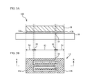
A description will now be given of a method of forming the inclination region 20 of the dielectric film 14. FIG. 3A through FIG. 4C are cross-sectional views illustrating a method of making the inclination region 20. As illustrated in FIG. 3A, the comb-shaped electrodes 12 a and 12 b are formed on the substrate 10. The dielectric film 14 are formed on the substrate 10 so as to cover the comb-shaped electrodes 12 a and 12 b. As illustrated in FIG. 3B, a photoresist 30 is applied on the dielectric film 14. As illustrated in FIG. 3C, the photoresist 30 on the bus bar 11 b is irradiated with an ultraviolet light UV with using an exposure mask 32. As illustrated in FIG. 3D, removed by development is the photoresist 30 on the bus bar 11 b irradiated with the ultraviolet light.
As illustrated in FIG. 4A, the inclination of an edge surface 35 of the photoresist 30 becomes large by postbake. As illustrated in FIG. 4B, the photoresist 30 and the dielectric film 14 are dry-etched by using etching-gas having a small selection ratio between the photoresist 30 and the dielectric film 14. This transfers the inclination of the edge surface 35 of the photoresist 30 to the dielectric film 14, and forms the inclination region 20 above the gaps 15. As illustrated in FIG. 4C, the photoresist 30 is removed. The inclination region 20 of the dielectric film 14 can be formed by the above-described process.
Next, measured and compared are conductances in a high-frequency signal between the comb-shaped electrodes 12 a and 12 b of the resonators in accordance with the first comparative example and the first embodiment. The measured resonator 100 in accordance with the first embodiment is the resonator of which the outline is illustrated in FIG. 1A through FIG. 2B. The substrate 10 mainly includes lithium niobium oxide. The comb-shaped electrodes 12 a and 12 b mainly include Cu. The dielectric film 14 mainly includes silicon oxide. Respective lengths of the electrode fingers 13 a and 13 b are approximately 30λ when λ is a wavelength of an acoustic wave that fulfills the function as an acoustic wave device. A length of the gap 15 is approximately 0.25λ. A film thickness of the dielectric film 14 on the electrode fingers 13 a and 13 b is approximately 0.3λ. A film thickness of the dielectric film 14 on the bus bars 11 a and 11 b is approximately 0.1λ. The inclination angle θ is approximately 35°. A length of a base of the inclination region 20 is approximately 0.35λ.
FIG. 5A is a cross-sectional view of a resonator 120 in accordance with the first comparative example, and FIG. 5B is a plain view of a part of the resonator 120. Referring to FIG. 5A and FIG. 5B, the upper surface of the dielectric film 14 above the gaps 15 is flat in the resonator 120 in accordance with the first comparative example as compared to FIG. 1A and FIG. 1B of the first embodiment. Other structures are the same as those of the resonator 100 in accordance with the first embodiment, and a description is omitted.
FIG. 6A and FIG. 6B are diagrams illustrating a conductance against a frequency in the resonators in accordance with the first embodiment and the first comparative example respectively. The frequency is around an anti-resonance frequency of the resonator. As illustrated in FIG. 6A, the conductance is relatively smooth against the frequency in the resonator 100 in accordance with the first embodiment. On the other hand, as illustrated in FIG. 6B, there are frequencies at which the conductance becomes a local maximum in the resonator 120 in accordance with the first comparative example. This is caused by the lateral-mode spurious.
Next, a distribution of the acoustic wave in the extension direction of the electrode fingers is measured. FIG. 7A and FIG. 7B are diagrams illustrating an intensity of an acoustic wave in the resonators in accordance with the first embodiment and the first comparative example respectively. FIG. 7A and FIG. 7B illustrate the intensity of the acoustic wave in the extension direction of the electrode fingers 13 a and 13 b when a drive signal of 1910 MHz is applied to the IDT 12. A horizontal axis denotes a position Y in the extension direction of the electrode fingers 13 a and 13 b, and a vertical axis denotes a displacement amplitude I of the acoustic wave. As illustrated in FIG. 7B, a third-mode acoustic wave in the lateral mode is excited in the overlap region 52 between the bus bar regions 54 in the first comparative example. On the other hand, as illustrated in FIG. 7A, a large number of high-order mode acoustic waves are excited in the first embodiment. As a result, unlike FIG. 7B, a certain strong high-order mode acoustic wave is not excited.
The resonators 100 having an inclination angle θ of 80°, 70°, 45°, 35° and 33° are made in the first embodiment, and a lateral-mode spurious amount against the inclination angle θ is measured. FIG. 8 is a diagram depicting the lateral-mode spurious amount against the inclination angle θ in the first embodiment. The lateral-mode spurious amount is a spurious amount of the largest spurious in diagrams of the conductance against the frequency such as FIG. 6A and FIG. 6B. As illustrated in FIG. 8, the lateral-mode spurious amount is large when the inclination angle θ is large. As the inclination angle θ becomes smaller, the lateral-mode spurious amount becomes smaller. Especially, when the inclination angle θ is equal to or smaller than 45°, the lateral-mode spurious is rarely observed. This is because the width of the inclination region 20 becomes narrow when the inclination angle θ becomes large, and the width of the inclination region 20 in the gap region 50 becomes small.
FIG. 9A is a cross-sectional view of a resonator 122 in accordance with a second comparative example, and FIG. 9B is a plain view of a part of the resonator 122. Compared to FIG. 1A and FIG. 1B of the first embodiment, the inclination region 20 is located in the bus bar regions 54, and the upper surface of the dielectric film 14 above the gaps 15 is flat in the resonator 122 in accordance with the second comparative example, as illustrated in FIG. 9A and FIG. 9B. Other structures are the same as those of the resonator 100 in accordance with the first embodiment, and a description is omitted.
FIG. 10 is a diagram illustrating a conductance against a frequency in the resonator in accordance with the second comparative example. As illustrated in FIG. 10, although the spurious is small compared to the first comparative example, a large lateral-mode spurious is observed compared to the first embodiment. As described above, it is possible to suppress the lateral-mode spurious by forming the inclination region 20 above the gaps 15.
FIG. 11 is a diagram illustrating characteristics of the conductance against the frequency. FIG. 11 is an example illustrating a relation between the frequency and the conductance, and a resonance frequency and the like do not correspond to those of the first comparative example and the first embodiment illustrated in FIG. 6A and FIG. 6B. In the example of FIG. 11, the resonance frequency fr is around 1750 MHz, and the anti-resonance frequency is around 1810 MHz. Here, the lateral-mode spurious is classified into a lateral-mode spurious within a frequency range 40 between the resonance frequency and the anti-resonance frequency, and a lateral-mode spurious within a frequency range 42 around the anti-resonance frequency. In addition to the frequency range 42, the lateral-mode spurious amount against the inclination angle θ is also measured within the frequency range 40.
FIG. 12 is a diagram illustrating the lateral-mode spurious amount against the inclination angle within different frequency ranges. In FIG. 12, black circles denote measurement results within the frequency range 42, and a solid line is an approximate curve of the black circles. Open circles denote measurement results within the frequency range 40, and a dashed line is an approximate curve of the open circles. The measurement points within the frequency range 42 are the same as those in FIG. 8. The lateral-mode spurious amount within the frequency range 42 is measured when the inclination angle θ is approximately 24°, 28°, 38° and 55°. When the inclination angle θ is 38°, the lateral-mode spurious is smallest. The lateral-mode spurious amount takes a local minimum value in the approximate curve when the inclination angle θ is around 40° to 45°. As described above, when the lateral-mode spurious around the frequency range 42 is a problem, it is preferable that the inclination angle θ is equal to or smaller than 45° as illustrated in FIG. 8. On the other hand, when the lateral-mode spurious around the frequency range 40 is a problem, the best inclination angle θ is different from that of the frequency range 42. According to FIG. 12, it is preferable that the inclination angle θ is equal to or larger than 30° and equal to or smaller than 50° in order to make the lateral-mode spurious amount equal to or smaller than 0.0025 S around the frequency range 40. Furthermore, the inclination angle θ is more preferably equal to or larger than 32° and equal to or smaller than 48°, and is further preferably equal to or larger than 35° and equal to or smaller than 45°. The characteristic of the acoustic wave can be generalized by being normalized by the wavelength λ of the acoustic wave. Thus, the inclination angle θ does not depend on λ. Therefore, FIG. 12 can be generalized to a resonator having a different resonance frequency.
According to the first embodiment, the upper surface of the dielectric film 14 above the gaps 15 is inclined against the upper surface of the substrate 10 in the extension direction of the electrode fingers 13 a and 13 b, and the inclination angle of the upper surface of the dielectric film 14 against the upper surface of the substrate 10 is equal to or larger than 30° and equal to or smaller than 50°. This enables to suppress the lateral-mode spurious especially within the frequency range 40 between the resonance frequency and the anti-resonance frequency. Furthermore, it is possible to suppress the degradation of reliability because the bus bars 11 a and 11 b can be covered with the dielectric film 14.
Called a normal type electrode is a resonator of which the overlap region is constant in a propagation direction of main acoustic wave as described in the first embodiment. It is also considered to apply apodization weighting that applies weighting to the overlap region in order to suppress the lateral-mode spurious. In the first embodiment, it is possible to suppress the lateral-mode spurious, and the apodization weighting is not necessary. Furthermore, an apodization weighted resonator may have the inclination region 20 in the gap region 50 as described in the first embodiment in order to further suppress the lateral-mode spurious.
Although it is sufficient if the inclination region 20 includes at least a part of the gap region 50, it is preferable that the upper surface of the dielectric film 14 is inclined across the entire region above the gaps 15 as illustrated in FIG. 1A and FIG. 1B of the first embodiment. This enables to further suppress the lateral-mode spurious. The inclination region 20 may include a part of the overlap region 52 and the bus bar regions 54.
Furthermore, the film thickness of the dielectric film 14 on the electrode fingers 13 a and 13 b is different from the film thickness of the dielectric film 14 on the bus bars 11 a and 11 b. This enables to make the inclination of the dielectric film 14 above the gaps 15 without exposing surfaces of bus bars 11 from the dielectric film 14.
Furthermore, the difference of film thickness in the dielectric film 14 caused by the inclination of the upper surface of the dielectric film 14 is larger than the film thicknesses of the opposing comb-shaped electrodes 12 a and 12 b. This enables to further reflect the acoustic wave in the lateral mode in the inclination region 20. Therefore, it is possible to further suppress the lateral-mode spurious.
A description will now be given of a first variation of the first embodiment. FIG. 13A is a cross-sectional view of a resonator 102 in accordance with the first variation of the first embodiment, and FIG. 13B is a plain view of a part of the resonator 102. As illustrated in FIG. 13A and FIG. 13B, the dielectric film 14 in the bus bar regions 54 is thicker than the dielectric film 14 in the overlap region 52 in the resonator 102 in accordance with the first variation of the first embodiment compared to FIG. 1A and FIG. 1B of the first embodiment. Other structures are the same as those of the resonator 100 in accordance with the first embodiment, and a description is omitted. The dielectric film 14 in the bus bar regions 54 may be thinner than the dielectric film 14 in the overlap region 52 as described in the first embodiment, and vice versa as described in the first variation of the first embodiment.
A description will now be given of a second variation of the first embodiment. FIG. 14A is a cross-sectional view of a resonator 104 in accordance with the second variation of the first embodiment, and FIG. 14B is a plain view of a part of the resonator 104. As illustrated in FIG. 14A and FIG. 14B, dummy electrode fingers 17 b and 17 a of the opposing comb-shaped electrodes 12 b and 12 a are located in the extension direction of tips of the electrode fingers 13 a and 13 b in the resonator 104 in accordance with the second variation of the first embodiment compared to FIG. 1A and FIG. 1B of the first embodiment. The dummy electrode fingers 17 a and 17 b are connected to the bus bars 11 a and 11 b respectively. Regions of the dummy electrode fingers 17 a and 17 b are dummy regions 56. The inclination region 20 is formed in the gap region 50. Other structures are the same as those in FIG. 1A and FIG. 1B of the first embodiment, and a description is omitted. The dummy electrode fingers 17 a and 17 b may be provided to the resonator 104 as described in the second variation of the first embodiment. The inclination region 20 may include a part of the overlap region 52, the bus bar regions 54 and the dummy regions 56. The dummy electrode may be provided to first, third, fourth or fifth variation of the first embodiment.
A description will now be given of a third variation of the first embodiment. FIG. 15A is a cross-sectional view of a resonator 106 in accordance with the third variation of the first embodiment, and FIG. 15B is a plain view of a part of the resonator 106. As illustrated in FIG. 15A and FIG. 15B, the inclination region 20 includes a first inclination region 20 a and a second inclination region 20 b in the resonator 106 in accordance with the third variation of the first embodiment compared to FIG. 1A and FIG. 1B of the first embodiment. The first inclination region 20 a is inclined so that the upper surface of the dielectric film 14 declines from the overlap region 52 side toward the bus bar regions 54 side. The second inclination region 20 b is inclined so that the upper surface of the dielectric film 14 ascends from the overlap region 52 side toward the bus bar regions 54 side. The first inclination region 20 a is located at the overlap region 52 side of the gap region 50, and the second inclination region 20 b is located at the bus bar regions 54 side of the gap region 50. Furthermore, the inclination region 20 is not located at the bus bar regions 54 side of the inclination region 20. Other structures are the same as those in FIG. 1A and FIG. 1B of the first embodiment, and a description is omitted. The inclination region 20 may include the first inclination region 20 a and the second inclination region 20 b as described in the third variation of the first embodiment. In addition, the inclination region 20 may be formed in a part of the gap region 50. Furthermore, an inclination angle θa of the first inclination region 20 a may be the same as or different from an inclination angle θb of the second inclination region 20 b. It is preferable that at least one of the inclination angles θa and θb is equal to or larger than 30° and equal to or smaller than 50°. It is more preferable that both of the inclination angles θa and θb are equal to or larger than 30° and equal to or smaller than 50°. Furthermore, it is preferable that the inclination angle θa is equal to or larger than 30° and equal to or smaller than 50° in order to distribute the acoustic wave propagated to the extension direction of the electrode fingers 13 a and 13 b.
A description will now be given of a fourth variation of the first embodiment. FIG. 16A is a cross-sectional view of a resonator 108 in accordance with the fourth variation of the first embodiment, and FIG. 16B is a plain view of a part of the resonator 108. As illustrated in FIG. 16A and FIG. 16B, another dielectric film 14 a is formed on the dielectric film 14 located in the second inclination region 20 b and the bus bar regions 54 of the resonator 108 in the fourth variation compared to FIG. 15A and FIG. 15B of the third variation of the first embodiment. The dielectric film 14 a is a silicon oxide film for example. Other structures are the same as FIG. 15A and FIG. 15B of the third variation of the first embodiment, and a description is omitted. The film thickness of the dielectric film 14 may be thick in a part of the gap region 50 as described in the fourth variation of the first embodiment.
A description will now be given of a fifth variation of the first embodiment. FIG. 17 is a plain view of a resonator 110 in accordance with a fifth variation of the first embodiment. As illustrated in FIG. 17, the inclination region 20 is located between the gap region 50 of the IDT 12 and the reflectors 16 of the IDT 12. Other structures are the same as those of the resonator 100 in accordance with the first embodiment, and a description is omitted. It is sufficient if the inclination region 20 is located in the gap region 50 of the comb-shaped electrodes 12 a and 12 b as described in the fifth variation of the first embodiment. For example, it is sufficient if the inclination region 20 is located only in the gap region 50 of the IDT 12.
The substrate 10 is a piezoelectric substance in the first embodiment and the variations of the first embodiment, but it is sufficient if at least one of the substrate 10 and the dielectric film 14 is a piezoelectric substance.
Second Embodiment
The second embodiment is an exemplary filter as the acoustic wave device. FIG. 18 is a circuit diagram of a ladder-type filter 115 in accordance with the second embodiment. As illustrated in FIG. 18, series resonators S1 through S3 are connected in series between an input terminal Tin and an output terminal Tout. Parallel resonator P1 and P2 are connected in parallel between the input terminal Tin and the output terminal Tout. One ends of the parallel resonator P1 and P2 are connected to a ground Gnd.
FIG. 19 is a plain view of the ladder-type filter 115 in accordance with the second embodiment. The series resonators S1 through S3 and the parallel resonators P1 and P2 are formed on the substrate 10 having a piezoelectricity. The series resonators S1 through S3 and the parallel resonators P1 and P2 are the resonator in accordance with the first embodiment or the variations of the first embodiment. The resonators are electrically interconnected via wirings 22. Each resonator includes the IDT 12, and the reflectors 16 sandwiching the IDT 12.
FIG. 20 is a diagram depicting measurement results of pass characteristics of the ladder-type filter 115 in accordance with the second embodiment. Each resonator of the ladder-type filter 115 of the second embodiment has the same structure as the resonator 100 of the first embodiment with which FIG. 6A is measured, and has an inclination angle θ of 35°. Each resonator of the ladder-type filter of the third comparative example has the same structure as the resonator 120 of the first comparative example with which FIG. 6B is measured. As illustrated in FIG. 20, a ripple caused by the lateral-mode spurious within the passband is small in the second embodiment as compared to the third comparative example.
The filter can be formed by using the first embodiment and the variations of the first embodiment as described in the second embodiment. The second embodiment is an example of the ladder-type filter, but the first embodiment or the variations of the first embodiment may be used to a multimode filter. Thus, it is possible to suppress a ripple within the passband.
The passband is around the resonance frequency of the series resonators S1 through S3 in the ladder-type filter. On the other hand, the passband is around the anti-resonance frequency of the parallel resonators P1 and P2. Therefore, the inclination angle θ of the series resonators S1 through S3 is made to be within a range of 30° to 50° (e.g. 45°). This enables to suppress the lateral-mode spurious between the resonance frequency and the anti-resonance frequency as illustrated in FIG. 12. On the other hand, the inclination angle θ of the parallel resonators P1 and P2 is made to be smaller than 45°. This enables to suppress the lateral-mode spurious around the anti-resonance frequency of the parallel resonators P1 and P2. For example, it is possible to suppress the lateral-mode spurious around the anti-resonance frequency of the parallel resonators P1 and P2 easily regardless of the variability of angles by making the inclination angle θ of the parallel resonators P1 and P2 30° for example. Therefore, it is possible to further suppress the ripple within the passband.
As described above, it is possible to make the inclination angles θ of the IDTs 12 different from each other in the acoustic wave device having multiple IDTs 12. For example, the inclination angle θ is made to be 30° to 50° in the resonator desired to suppress the lateral-mode spurious between the resonance frequency and the anti-resonance frequency. Preferably, it is made to be 35° to 45°. The inclination angle θ is made to be equal to or smaller than 45° in the resonator desired to suppress the lateral-mode spurious around the anti-resonance frequency. Preferably, it is made to be equal to or smaller than 35°, further preferably, to be equal to or smaller than 30°. This enables to further suppress the lateral-mode spurious. As described above, it is possible to make the inclination angle θ of a first IDT included in the series resonators S1 through S3 different from that of a second IDT included in the parallel resonators P1 and P2.
The second embodiment may use the resonator in accordance with the variations of the first embodiment besides the resonator in accordance with the first embodiment.
Third Embodiment
A third embodiment is an exemplary RF (Radio Frequency) module. FIG. 21 is a block diagram of a module 70 in accordance with the third embodiment. As illustrated in FIG. 21, the module 70 mainly includes a duplexer 73, a power amplifier 74, a transmission filter 75, a low noise amplifier 76 and a reception filter 77. The duplexer 73 has filters 71 and 72. A transmission signal is input to the transmission terminal Ttx. The transmission filter 75 filters the transmission signal. The power amplifier 74 amplifies the transmission signal. The filter 71 of the duplexer 73 filters the transmission signal, and outputs the transmission signal to the antenna terminal Tant. The filter 72 of the duplexer 73 suppresses the leakage of the transmission signal to the low noise amplifier 76 side. A reception signal is input to the antenna terminal Tant. The filter 72 of the duplexer 73 outputs the reception signal to the low noise amplifier 76. The filter 71 of the duplexer 73 suppresses the leakage of the reception signal to the power amplifier 74 side. The low noise amplifier 76 amplifies the reception signal. The reception filter 77 filters the reception signal, and outputs it to the reception terminal Trx.
At least one of the filters 71, 72, 75 and 77 may be the filter of the second embodiment in the module 70 in accordance with the third embodiment. The module 70 in accordance with the third embodiment can be used as an RF module for mobile communication such as mobile phones for example. Besides the third embodiment, the resonator of the first embodiment or the variations of the first embodiment can be used to the module.
Although the embodiments of the present invention have been described in detail, it should be understood that the present invention is not limited to these specific embodiments, and the various change, substitutions, and alterations could be made hereto without departing from the spirit and scope of the invention.

Claims (7)

What is claimed is:
1. An acoustic wave device comprising:
a substrate;
a dielectric film formed on the substrate;
opposing comb-shaped electrodes located between the substrate and the dielectric film, each of the opposing comb-shaped electrodes including an electrode finger, wherein
at least one of the substrate and the dielectric film is a piezoelectric substance,
an upper surface of the dielectric film, which is located above a gap between a tip of an electrode finger of one of the opposing comb-shaped electrodes and the other of the opposing comb-shaped electrodes, is inclined against an upper surface of the substrate in an extension direction of the electrode finger, and
an inclination angle of the upper surface of the dielectric film against the upper surface of the substrate is equal to or larger than 30° and equal to or smaller than 50°.
2. The acoustic wave device according to claim 1, wherein
the upper surface of the dielectric film is inclined across an entire region above the gap.
3. The acoustic wave device according to claim 1, wherein
each of the opposing comb-shaped electrodes includes the electrode finger and a bus bar, and a film thickness of the dielectric film on the electrode finger is different from a film thickness of the dielectric film on the bus bar.
4. The acoustic wave device according to claim 1, wherein
a difference of film thickness in the dielectric film caused by an inclination of the upper surface of the dielectric film is larger than film thicknesses of the opposing comb-shaped electrodes.
5. The acoustic wave device according to claim 1, further comprising:
IDTs, each including the opposing comb-shaped electrodes, wherein
the IDTs have different inclination angles.
6. The acoustic wave device according to claim 5, wherein
the IDTs include a first IDT included in a series resonator of a ladder-type filter, and a second IDT included in a parallel resonator of the ladder-type filter, and
the first IDT and the second IDT have different inclination angles.
7. A module comprising:
an acoustic wave device according to claim 1.
US13/725,514 2011-05-19 2012-12-21 Acoustic wave device and module including a dielectric film with an inclined upper surface Active 2032-01-03 US8896399B2 (en)

Applications Claiming Priority (1)

Application Number Priority Date Filing Date Title
PCT/JP2011/061471 WO2012157101A1 (en) 2011-05-19 2011-05-19 Acoustic wave device and module

Related Parent Applications (1)

Application Number Title Priority Date Filing Date
PCT/JP2011/061471 Continuation WO2012157101A1 (en) 2011-05-19 2011-05-19 Acoustic wave device and module

Publications (2)

Publication Number Publication Date
US20130106536A1 US20130106536A1 (en) 2013-05-02
US8896399B2 true US8896399B2 (en) 2014-11-25

Family

ID=47176464

Family Applications (1)

Application Number Title Priority Date Filing Date
US13/725,514 Active 2032-01-03 US8896399B2 (en) 2011-05-19 2012-12-21 Acoustic wave device and module including a dielectric film with an inclined upper surface

Country Status (4)

Country Link
US (1) US8896399B2 (en)
JP (1) JP5695191B2 (en)
SG (1) SG186395A1 (en)
WO (1) WO2012157101A1 (en)

Cited By (2)

* Cited by examiner, † Cited by third party
Publication number Priority date Publication date Assignee Title
US9083303B2 (en) * 2010-02-26 2015-07-14 Taiyo Yuden Co., Ltd. Acoustic wave device
US20210067134A1 (en) * 2019-08-29 2021-03-04 Skyworks Solutions, Inc. Suppression of transverse mode spurious signals in surface acoustic wave devices utilizing a dense film above gap region of interdigital transducer electrodes

Families Citing this family (5)

* Cited by examiner, † Cited by third party
Publication number Priority date Publication date Assignee Title
JP6335473B2 (en) * 2013-11-01 2018-05-30 太陽誘電株式会社 Surface acoustic wave device and filter
JP2018078419A (en) * 2016-11-08 2018-05-17 株式会社村田製作所 Acoustic wave device, high frequency front end circuit, and communication device
JP6947220B2 (en) 2017-09-05 2021-10-13 株式会社村田製作所 Filter device
JP7027079B2 (en) * 2017-09-12 2022-03-01 太陽誘電株式会社 Elastic wave device and its manufacturing method
CN116097563A (en) * 2020-08-19 2023-05-09 株式会社村田制作所 Elastic wave device

Citations (10)

* Cited by examiner, † Cited by third party
Publication number Priority date Publication date Assignee Title
US6940208B2 (en) * 2001-07-24 2005-09-06 Murata Manufacturing Co., Ltd. Surface acoustic wave device
JP2005244359A (en) 2004-02-24 2005-09-08 Murata Mfg Co Ltd Surface acoustic wave device, ladder type filter, and resonator type filter
WO2006078001A1 (en) 2005-01-21 2006-07-27 National University Corporation Chiba University Elastic surface wave device
JP2007110342A (en) 2005-10-12 2007-04-26 Kyocera Corp Surface acoustic wave element and manufacturing method thereof
WO2008078573A1 (en) 2006-12-27 2008-07-03 Panasonic Corporation Surface acoustic wave resonator, surface acoustic wave filter using the surface acoustic wave resonator, and antenna duplexer
JP2009290472A (en) * 2008-05-28 2009-12-10 Fujitsu Ltd Elastic wave device, filter, communication module and communication device
WO2010137279A1 (en) 2009-05-27 2010-12-02 パナソニック株式会社 Acoustic wave resonator and duplexer using same
US20110215884A1 (en) * 2010-03-02 2011-09-08 Panasonic Corporation Ladder-type filter
US20110215883A1 (en) * 2010-03-02 2011-09-08 Panasonic Corporation Acoustic wave resonator and acoustic wave filter using the same
US20120313483A1 (en) * 2010-02-26 2012-12-13 Taiyo Yuden Co., Ltd. Acoustic wave device

Patent Citations (14)

* Cited by examiner, † Cited by third party
Publication number Priority date Publication date Assignee Title
US7132779B2 (en) * 2001-07-24 2006-11-07 Murata Manufacturing Co., Ltd. Surface acoustic wave device
US6940208B2 (en) * 2001-07-24 2005-09-06 Murata Manufacturing Co., Ltd. Surface acoustic wave device
JP2005244359A (en) 2004-02-24 2005-09-08 Murata Mfg Co Ltd Surface acoustic wave device, ladder type filter, and resonator type filter
US20090206954A1 (en) 2005-01-21 2009-08-20 National University Corporation Chiba University Elastic surface wave device
WO2006078001A1 (en) 2005-01-21 2006-07-27 National University Corporation Chiba University Elastic surface wave device
JP2007110342A (en) 2005-10-12 2007-04-26 Kyocera Corp Surface acoustic wave element and manufacturing method thereof
WO2008078573A1 (en) 2006-12-27 2008-07-03 Panasonic Corporation Surface acoustic wave resonator, surface acoustic wave filter using the surface acoustic wave resonator, and antenna duplexer
US20100219905A1 (en) 2006-12-27 2010-09-02 Hiroyuki Nakamura Surface acoustic wave resonator, and surface acoustic wave filter and antenna duplexer in which the surface acoustic wave resonator is used
JP2009290472A (en) * 2008-05-28 2009-12-10 Fujitsu Ltd Elastic wave device, filter, communication module and communication device
WO2010137279A1 (en) 2009-05-27 2010-12-02 パナソニック株式会社 Acoustic wave resonator and duplexer using same
US20120044027A1 (en) 2009-05-27 2012-02-23 Hidekazu Nakanishi Acoustic wave resonator and duplexer using same
US20120313483A1 (en) * 2010-02-26 2012-12-13 Taiyo Yuden Co., Ltd. Acoustic wave device
US20110215884A1 (en) * 2010-03-02 2011-09-08 Panasonic Corporation Ladder-type filter
US20110215883A1 (en) * 2010-03-02 2011-09-08 Panasonic Corporation Acoustic wave resonator and acoustic wave filter using the same

Non-Patent Citations (3)

* Cited by examiner, † Cited by third party
Title
English translation of Written Opinion (PCT/ISA/237) issued in PCT/JP2011/061471 mailed in Jul. 2011.
International Search Report (ISR) issued in PCT/JP2011/061471 mailed in Jul. 2011.
Written Opinion (PCT/ISA/237) issued in PCT/JP2011/061471 mailed in Jul. 2011.

Cited By (3)

* Cited by examiner, † Cited by third party
Publication number Priority date Publication date Assignee Title
US9083303B2 (en) * 2010-02-26 2015-07-14 Taiyo Yuden Co., Ltd. Acoustic wave device
US20210067134A1 (en) * 2019-08-29 2021-03-04 Skyworks Solutions, Inc. Suppression of transverse mode spurious signals in surface acoustic wave devices utilizing a dense film above gap region of interdigital transducer electrodes
US11652466B2 (en) * 2019-08-29 2023-05-16 Skyworks Solutions, Inc. Suppression of transverse mode spurious signals in surface acoustic wave devices utilizing a dense film above gap region of interdigital transducer electrodes

Also Published As

Publication number Publication date
WO2012157101A1 (en) 2012-11-22
SG186395A1 (en) 2013-01-30
JP5695191B2 (en) 2015-04-01
US20130106536A1 (en) 2013-05-02
JPWO2012157101A1 (en) 2014-07-31

Similar Documents

Publication Publication Date Title
US8896399B2 (en) Acoustic wave device and module including a dielectric film with an inclined upper surface
US9306539B2 (en) Resonator, filter, and duplexer
CN106664074B (en) Elastic wave element, filter element, and communication device
US9722575B2 (en) Duplexer
US10361678B2 (en) Acoustic wave resonator, filter, and duplexer
US20130099875A1 (en) Acoustic wave device and antenna duplexer employing the same
JP4727322B2 (en) Surface acoustic wave device
US7482896B2 (en) Surface acoustic wave apparatus
CN107070431B (en) Acoustic wave resonator, filter, and duplexer
JPH08265087A (en) Surface acoustic wave filter
US10270425B2 (en) Acoustic wave resonator, filter, and multiplexer
US20160285431A1 (en) Surface acoustic wave filter
US8049583B2 (en) Acoustic wave filter comprising a reflector having an oblique slit
JP2003188675A (en) Surface acoustic wave element and duplexer provided therewith
US10763822B2 (en) Acoustic wave resonator, filter, and multiplexer
JP2018182460A (en) Acoustic wave resonator, filter, and multiplexer
US6933803B2 (en) Surface acoustic wave filter, branching filter, and communication apparatus
CA2375596A1 (en) Longitudinally coupled surface acoustic wave filter
JP2003032080A (en) Saw resonator and ladder type saw filter
JPH10261935A (en) Surface acoustic wave element
US11451210B2 (en) Acoustic wave device, filter, and multiplexer
KR100599244B1 (en) Edge reflection type surface acoustic wave filter
JP6585459B2 (en) Elastic wave device, duplexer, and communication device
JPH10261936A (en) Surface acoustic wave filter
JP6780323B2 (en) Elastic surface wave element, elastic surface wave filter and multiplexer

Legal Events

Date Code Title Description
AS Assignment

Owner name: TAIYO YUDEN CO., LTD., JAPAN

Free format text: ASSIGNMENT OF ASSIGNORS INTEREST;ASSIGNORS:MIURA, MICHIO;MATSUDA, SATORU;YAMASHITA, TAKASHI;AND OTHERS;SIGNING DATES FROM 20120907 TO 20120926;REEL/FRAME:029522/0731

STCF Information on status: patent grant

Free format text: PATENTED CASE

FEPP Fee payment procedure

Free format text: PAYOR NUMBER ASSIGNED (ORIGINAL EVENT CODE: ASPN); ENTITY STATUS OF PATENT OWNER: LARGE ENTITY

MAFP Maintenance fee payment

Free format text: PAYMENT OF MAINTENANCE FEE, 4TH YEAR, LARGE ENTITY (ORIGINAL EVENT CODE: M1551)

Year of fee payment: 4

MAFP Maintenance fee payment

Free format text: PAYMENT OF MAINTENANCE FEE, 8TH YEAR, LARGE ENTITY (ORIGINAL EVENT CODE: M1552); ENTITY STATUS OF PATENT OWNER: LARGE ENTITY

Year of fee payment: 8