WO2012144450A1 - 表示装置 - Google Patents
表示装置 Download PDFInfo
- Publication number
- WO2012144450A1 WO2012144450A1 PCT/JP2012/060239 JP2012060239W WO2012144450A1 WO 2012144450 A1 WO2012144450 A1 WO 2012144450A1 JP 2012060239 W JP2012060239 W JP 2012060239W WO 2012144450 A1 WO2012144450 A1 WO 2012144450A1
- Authority
- WO
- WIPO (PCT)
- Prior art keywords
- insulating film
- substrate
- opening
- film
- display device
- Prior art date
- Legal status (The legal status is an assumption and is not a legal conclusion. Google has not performed a legal analysis and makes no representation as to the accuracy of the status listed.)
- Ceased
Links
Images





Classifications
-
- G—PHYSICS
- G02—OPTICS
- G02F—OPTICAL DEVICES OR ARRANGEMENTS FOR THE CONTROL OF LIGHT BY MODIFICATION OF THE OPTICAL PROPERTIES OF THE MEDIA OF THE ELEMENTS INVOLVED THEREIN; NON-LINEAR OPTICS; FREQUENCY-CHANGING OF LIGHT; OPTICAL LOGIC ELEMENTS; OPTICAL ANALOGUE/DIGITAL CONVERTERS
- G02F1/00—Devices or arrangements for the control of the intensity, colour, phase, polarisation or direction of light arriving from an independent light source, e.g. switching, gating or modulating; Non-linear optics
- G02F1/01—Devices or arrangements for the control of the intensity, colour, phase, polarisation or direction of light arriving from an independent light source, e.g. switching, gating or modulating; Non-linear optics for the control of the intensity, phase, polarisation or colour
- G02F1/13—Devices or arrangements for the control of the intensity, colour, phase, polarisation or direction of light arriving from an independent light source, e.g. switching, gating or modulating; Non-linear optics for the control of the intensity, phase, polarisation or colour based on liquid crystals, e.g. single liquid crystal display cells
- G02F1/133—Constructional arrangements; Operation of liquid crystal cells; Circuit arrangements
- G02F1/1333—Constructional arrangements; Manufacturing methods
- G02F1/133345—Insulating layers
-
- G—PHYSICS
- G02—OPTICS
- G02F—OPTICAL DEVICES OR ARRANGEMENTS FOR THE CONTROL OF LIGHT BY MODIFICATION OF THE OPTICAL PROPERTIES OF THE MEDIA OF THE ELEMENTS INVOLVED THEREIN; NON-LINEAR OPTICS; FREQUENCY-CHANGING OF LIGHT; OPTICAL LOGIC ELEMENTS; OPTICAL ANALOGUE/DIGITAL CONVERTERS
- G02F1/00—Devices or arrangements for the control of the intensity, colour, phase, polarisation or direction of light arriving from an independent light source, e.g. switching, gating or modulating; Non-linear optics
- G02F1/01—Devices or arrangements for the control of the intensity, colour, phase, polarisation or direction of light arriving from an independent light source, e.g. switching, gating or modulating; Non-linear optics for the control of the intensity, phase, polarisation or colour
- G02F1/13—Devices or arrangements for the control of the intensity, colour, phase, polarisation or direction of light arriving from an independent light source, e.g. switching, gating or modulating; Non-linear optics for the control of the intensity, phase, polarisation or colour based on liquid crystals, e.g. single liquid crystal display cells
- G02F1/133—Constructional arrangements; Operation of liquid crystal cells; Circuit arrangements
- G02F1/1333—Constructional arrangements; Manufacturing methods
- G02F1/1339—Gaskets; Spacers; Sealing of cells
-
- G—PHYSICS
- G02—OPTICS
- G02F—OPTICAL DEVICES OR ARRANGEMENTS FOR THE CONTROL OF LIGHT BY MODIFICATION OF THE OPTICAL PROPERTIES OF THE MEDIA OF THE ELEMENTS INVOLVED THEREIN; NON-LINEAR OPTICS; FREQUENCY-CHANGING OF LIGHT; OPTICAL LOGIC ELEMENTS; OPTICAL ANALOGUE/DIGITAL CONVERTERS
- G02F1/00—Devices or arrangements for the control of the intensity, colour, phase, polarisation or direction of light arriving from an independent light source, e.g. switching, gating or modulating; Non-linear optics
- G02F1/01—Devices or arrangements for the control of the intensity, colour, phase, polarisation or direction of light arriving from an independent light source, e.g. switching, gating or modulating; Non-linear optics for the control of the intensity, phase, polarisation or colour
- G02F1/13—Devices or arrangements for the control of the intensity, colour, phase, polarisation or direction of light arriving from an independent light source, e.g. switching, gating or modulating; Non-linear optics for the control of the intensity, phase, polarisation or colour based on liquid crystals, e.g. single liquid crystal display cells
- G02F1/133—Constructional arrangements; Operation of liquid crystal cells; Circuit arrangements
- G02F1/1333—Constructional arrangements; Manufacturing methods
- G02F1/1343—Electrodes
- G02F1/134309—Electrodes characterised by their geometrical arrangement
- G02F1/134372—Electrodes characterised by their geometrical arrangement for fringe field switching [FFS] where the common electrode is not patterned
-
- G—PHYSICS
- G02—OPTICS
- G02F—OPTICAL DEVICES OR ARRANGEMENTS FOR THE CONTROL OF LIGHT BY MODIFICATION OF THE OPTICAL PROPERTIES OF THE MEDIA OF THE ELEMENTS INVOLVED THEREIN; NON-LINEAR OPTICS; FREQUENCY-CHANGING OF LIGHT; OPTICAL LOGIC ELEMENTS; OPTICAL ANALOGUE/DIGITAL CONVERTERS
- G02F2201/00—Constructional arrangements not provided for in groups G02F1/00 - G02F7/00
- G02F2201/50—Protective arrangements
- G02F2201/503—Arrangements improving the resistance to shock
-
- G—PHYSICS
- G02—OPTICS
- G02F—OPTICAL DEVICES OR ARRANGEMENTS FOR THE CONTROL OF LIGHT BY MODIFICATION OF THE OPTICAL PROPERTIES OF THE MEDIA OF THE ELEMENTS INVOLVED THEREIN; NON-LINEAR OPTICS; FREQUENCY-CHANGING OF LIGHT; OPTICAL LOGIC ELEMENTS; OPTICAL ANALOGUE/DIGITAL CONVERTERS
- G02F2202/00—Materials and properties
- G02F2202/28—Adhesive materials or arrangements
Definitions
- the present invention relates to a display device used for various purposes such as a mobile phone, a digital camera, a portable game machine, or a portable information terminal.
- the display device includes a first substrate and a second substrate arranged to face each other, a liquid crystal layer provided between the substrates, a first substrate and the second substrate, and a sealing material made of an organic material. Provided (see, for example, JP 2009-128893 A).
- a plurality of source lines and a plurality of gate lines are provided on the main surface of the second substrate so as to intersect each other.
- a planarizing film made of an organic material is provided so as to cover the source wiring and the gate wiring.
- a display electrode is provided on the planarizing film and in a region surrounded by a plurality of source lines and a plurality of gate lines.
- the planarizing film is provided in a region overlapping the first substrate in the main surface of the second substrate, the second substrate in the overlapping region can be planarized, and the first substrate and the second substrate can be planarized. Can be made uniform between the first substrate and the second substrate.
- the planarizing film is provided in a region of the main surface of the second substrate that overlaps the first substrate, the planarizing film is located in a region where the sealing material is formed on the second substrate.
- the sealing material adheres to the planarization film on the second substrate.
- the sealing material since the adhesiveness between the sealing material and the planarizing film made of an organic material is low, the sealing material is easily peeled off from the planarizing film, and the adhesive strength between the first substrate and the second substrate may be reduced.
- display devices in recent years tend to have a narrower frame in addition to an increase in the size of the display screen, and since the area where the sealing material is formed is also reduced, the sealing material is peeled off due to stress due to dropping impact, twisting, etc. The danger is increasing.
- the present invention has been made in view of the above problems, and an object thereof is to suppress a decrease in the adhesive strength of the sealing material in the display device.
- the display device of the present invention includes a first substrate and a second substrate that are disposed so that inner main surfaces face each other, a liquid crystal layer that is disposed between the first substrate and the second substrate, and the liquid crystal layer.
- a sealing material disposed between the first substrate and the second substrate so as to surround the first substrate and the second substrate; and the seal on the inner main surface of the second substrate.
- An organic insulating film having an opening in the seal forming region provided in the seal forming region where the material is formed, and continuously from the inside of the opening through the inner wall surface of the opening to the surface of the organic insulating film And an inorganic insulating film provided in contact with and covering the sealing material.
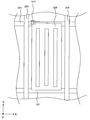
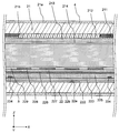
- FIG. 2 is a cross-sectional view taken along the line II of FIG. It is a top view which shows the electrode, wiring, and thin-film transistor which were formed on the 2nd board
- FIG. 2 is a cross-sectional view taken along line II-II in FIG. It is a figure which shows the relationship between the wiring conductor in a seal
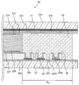
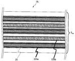
- FIG. 9 is a plan view showing a relationship between a wiring conductor and a first opening and a second opening of a second planarization film in the seal formation region in the display device of FIG. 8. It is sectional drawing which shows the principal part of the liquid crystal panel in the 3rd Embodiment of this invention. It is sectional drawing which shows the principal part of the liquid crystal panel in the 4th Embodiment of this invention. It is sectional drawing which shows the principal part of the liquid crystal panel in the 5th Embodiment of this invention.
- the display device 1 includes a liquid crystal panel 2, a light source device 3 that emits light toward the liquid crystal panel 2, a first polarizing plate 4 disposed on the liquid crystal panel 2, and between the liquid crystal panel 2 and the light source device 3.
- the 2nd polarizing plate 5 arrange
- the electric field is generated between the signal electrode provided on one of the pair of substrates (second substrate 22) and the common electrode, and the direction of the liquid crystal molecules in the liquid crystal layer
- the so-called lateral electric field method for controlling the above is adopted.
- the liquid crystal panel 2 in this embodiment employ
- a vertical electric field method may be adopted.
- the first substrate 21 and the second substrate 22 are disposed to face each other, and a liquid crystal layer 23 is provided between the first substrate 21 and the second substrate 22, so as to surround the liquid crystal layer 23.
- a sealing material 24 for joining the first substrate 21 and the second substrate 22 is provided.
- the second main surface 21b and the first major surface 22a of the second substrate 22 of the first substrate 21, the sealing formation region E 24 sealing material 24 is formed, the inner region surrounded by the sealant 24 E I and the sealant It has an outer region EO located outside 24.
- the first substrate 21 has a first main surface 21a used as a display surface when displaying an image, and a second main surface 21b located on the opposite side of the first main surface 21a.
- the first substrate 21 is formed of a light-transmitting material such as glass or plastic.
- a light shielding film 211 On the second main surface 21b of the first substrate 21, a light shielding film 211, a color filter 212, a first planarization film 213, and a first alignment film 214 are provided.
- the light shielding film 211 is provided on the second main surface 21b of the first substrate 21 in a lattice shape along the outer periphery of each pixel P.
- Examples of the material of the light shielding film 211 include a resin to which a dye or pigment having a high light shielding property (for example, black) is added, or a metal such as chromium.
- the light shielding film 211 in the present embodiment is formed in a lattice shape on the second main surface 21b, the present invention is not limited to this.
- the color filter 212 has a function of transmitting only a specific wavelength of visible light.
- the plurality of color filters 212 are located on the second main surface 21 b of the first substrate 21 and are provided for each pixel P.
- Each color filter 212 has one of red (R), green (G), and blue (B). Further, the color filter 212 is not limited to the above color, and may have a color such as yellow (Y) or white (W), for example.
- Examples of the material of the color filter 212 include a resin to which a dye or a pigment is added.
- the first planarization film 213 has a function of planarizing the second main surface 21b of the first substrate 21.
- the first planarizing film 213 is provided on the light shielding film 211 and the color filter 212.
- the first planarizing film 213 is continuously formed from the inner region E I surrounded by the sealing material 24 passes through the seal forming region E 24 to the outer region E O.
- the first planarization film 213 is formed of an organic material, and examples of the organic material include acrylic resin, epoxy resin, and polyimide resin.
- the film thickness of the first planarizing film 213 is set in the range of 1 ⁇ m to 5 ⁇ m, for example.
- the first alignment film 214 has a function of controlling the alignment of liquid crystal molecules in the liquid crystal layer 23.
- the first alignment film 214 is provided on the first planarizing film 213 in the inner region E I.
- Examples of the material of the first alignment film 214 include a resin such as a polyimide resin.
- the second substrate 22 has a first main surface 22a facing the second main surface 21b of the first substrate 21 and a second main surface 22b located on the opposite side of the first main surface 22a.
- the second substrate 22 can be formed of the same material as the first substrate 21.
- a gate insulating film 222 to cover the plurality of gate lines 221.
- a first interlayer insulating film 223 is provided on the gate insulating film 222, and a plurality of source wirings 224 are provided on the first interlayer insulating film 223.
- a second planarizing film 225 is provided on the first interlayer insulating film 223 so as to cover the source wiring 224, and a common electrode 226 is provided on the second planarizing film 225.
- a second interlayer insulating film 227 is provided on the second planarizing film 225 so as to cover the common electrode 226, and a signal electrode 228 is provided on the second interlayer insulating film 227.
- a second alignment film 229 is provided on the second interlayer insulating film 227 so as to cover the signal electrode 228.
- the gate wiring 221 has a function of applying a voltage supplied from a driving IC (not shown) to the thin film transistor TFT. As shown in FIG. 3, the gate wiring 221 extends in the X direction on the first main surface 22 a of the second substrate 22. The plurality of gate wirings 221 are arranged along the Y direction.
- the gate wiring 221 is formed of a conductive material, for example, aluminum, molybdenum, titanium, neodymium, chromium, copper, or an alloy containing these.
- the following method can be given as a method for forming the gate wiring 221.
- a metal material is formed as a metal film on the first main surface 22a of the second substrate 22 by sputtering, vapor deposition, or chemical vapor deposition.
- a photosensitive resin is applied to the surface of the metal film, and a pattern having a desired shape is formed on the photosensitive resin by performing exposure processing and development processing on the applied photosensitive resin.
- the metal film is etched with a chemical solution to make the metal film into a desired shape, and then the applied photosensitive resin is peeled off.
- the gate wiring 221 can be formed by forming and patterning a metal material.
- the gate insulating film 222 is provided on the first main surface 22 a so as to cover the gate wiring 221.
- the gate insulating film 222 is formed using an insulating material such as silicon nitride or silicon oxide.
- the gate insulating film 222 is formed on the first main surface 22a of the second substrate 22 by the above sputtering method, vapor deposition method, or chemical vapor deposition method.
- the first interlayer insulating film 223 has a function of electrically insulating the gate wiring 221 and the source wiring 224.
- the first interlayer insulating film 223 is provided continuously from the inner region E I a seal formation region E 24 up through the outer region E O.
- the first interlayer insulating film 223 is formed of an insulating material, and examples thereof include inorganic materials such as silicon nitride and silicon oxide. In the display device 1, the first interlayer insulating film 223 is formed of silicon nitride.
- the first interlayer insulating film 223 can be formed by the same formation method as the gate insulating film 222.
- the source wiring 224 has a function of applying a signal voltage supplied from the driving IC to the signal electrode 228 via the thin film transistor TFT. As shown in FIG. 3, the plurality of source lines 224 extend in the Y direction. The plurality of source lines 224 are arranged on the first interlayer insulating film 223 along the X direction. The source wiring 224 may be formed using the same material as the gate wiring 221. The source wiring 224 can be formed by a method similar to that for forming the gate wiring 221.
- the thin film transistor TFT includes a semiconductor layer such as amorphous silicon or polysilicon, a source electrode provided on the semiconductor layer and connected to the source wiring 224, and a drain electrode provided on the semiconductor layer and connected to the signal electrode 228. And have.
- the resistance of the semiconductor layer between the source electrode and the drain electrode changes according to the voltage applied to the semiconductor layer via the gate wiring 221, thereby writing or non-writing the image signal to the signal electrode 228. Is controlled.
- the second planarization film 225 has a function of electrically insulating the source wiring 224 and the common electrode 226 and planarizing the first main surface 22 a of the second substrate 22.
- the second planarizing film 225 is formed continuously from the inner region E I to seal forming region E 24.
- the second planarization film 225 is formed of an organic material, for example, a resin such as an acrylic resin, an epoxy resin, or a polyimide resin.
- the film thickness of the second planarizing film 225 is set in the range of 1 ⁇ m to 5 ⁇ m, for example.
- the thickness of the second planarization film 225 is set to be thicker than the thickness of the first planarization film 213. Since the thin film transistor TFT, the plurality of electrodes, the plurality of wirings, and the like are formed on the second main surface 22a of the second substrate 22, the flatness is likely to deteriorate. Therefore, the flatness on the second main surface 22a of the second substrate 22 can be improved by making the film thickness of the second planarizing film 225 thicker than the film thickness of the first planarizing film 213.
- the common electrode 226 has a function of generating an electric field with the signal electrode 228 by a voltage applied from the driving IC.
- the common electrode 226 is provided on the second planarization film 225.
- the common electrode 226 is formed of a material having translucency and conductivity. It is formed of tin, zinc oxide or a conductive polymer.
- the second interlayer insulating film 227 has a function of electrically insulating the signal electrode 228 and the common electrode 226 from each other.
- the second interlayer insulating film 227 may be formed of the same material as the first interlayer insulating film 223.
- the second interlayer insulating film 227 is made of silicon oxide.
- the signal electrode 228 has a function of generating an electric field with the common electrode 226 by a voltage applied from the driving IC.
- the plurality of signal electrodes 228 are provided on the second interlayer insulating film 227 and are located for each pixel P.
- the signal electrode 228 may be formed of the same material as the common electrode 226.
- the common electrode 226, the second interlayer insulating film 227, and the signal electrode 228 are provided in this order, but the present invention is not limited to this. That is, the common electrode 226 may be formed on the signal electrode 228 with the second interlayer insulating film 227 interposed therebetween, and the signal electrode 228, the second interlayer insulating film 227, and the common electrode 226 may be provided in this order.
- the second alignment film 229 has a function of controlling the alignment of the liquid crystal molecules in the liquid crystal layer 23.
- the second alignment film 229 is provided on the second interlayer insulating film 227 so as to cover the signal electrode 228.
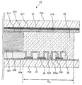
- the first interlayer insulating film 223 is located on the first main surface 22a of the second substrate 22 in the seal formation region E 24, the first interlayer insulating film 223 is located.
- a wiring conductor 25 is located on the first interlayer insulating film 223.
- a second planarizing film 225 having a first opening 225a is located on the first interlayer insulating film 223.
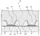
- the first inorganic insulating film 26 is located in the first opening 225 a of the second planarizing film 225.
- the wiring conductor 25 is formed on the first interlayer insulating film 223. Wiring conductor 25 is provided so as to overlap the sealing formation region E 24 through the seal forming region E 24.
- the wiring conductor 25 is connected to, for example, the gate wiring 221 or the source wiring 224.
- the wiring conductor 25 may be a so-called dummy wiring conductor that is not connected to a wiring or an electrode.
- the material of the wiring conductor 25 is formed of a conductive material such as aluminum, molybdenum, titanium, neodymium, chromium, copper, or an alloy containing these.
- the wiring conductor 25 is formed by the same method as the gate wiring 221.
- the second planarizing film 225 extends from the inner region E I the seal formation region E 24. Further, as shown in FIG. 5, the outer end of the second planarization film 225 is located inside the outer end of the sealing material 24. As a result, the first interlayer insulating film 223 is exposed from the second planarizing film 225 and adhered to the sealing material 24 between the outer end of the second planarizing film 225 and the outer end of the sealing material 24. Therefore, the adhesion area between the sealing material 24 and the first interlayer insulating film 223 can be increased. Accordingly, the sealing material 24 is difficult to peel off from the second substrate 22.
- the first interlayer insulating film 223 extends from the second planarization film 225 between the outer end of the second planarization film 225 and the outer end of the sealant 24 in the entire seal formation region E 24. Exposed. Thus, the entire seal forming region E 24, the sealing member 24 is hardly peeled off from over the second substrate 22.
- the second planarization film 225 located in the seal formation region E 24 has a first opening 225 a on the wiring conductor 25. That is, the wiring conductor 25 in the opening 225a is exposed from the second planarization film 225.
- FIG. 6A is a plan view showing the relationship between the wiring conductor 25 and the first opening 225a of the second planarization film 225 in the side E24a of the annular seal member 24 formed in FIG.
- FIG. 6B is a plan view showing the relationship between the wiring conductor 25 and the first opening 225a of the second planarizing film 225 at the corner E 24b of FIG.
- the outer periphery of the first opening 225a is indicated by a thick line.
- the first opening 225a is provided continuously along the region where the wiring conductor 25 is formed.
- the first opening 225a is also formed along the sealing material 24.
- the shape of the first opening 225a is not limited to the above shape.
- the holes may be scattered on the wiring conductor 25.
- the shape of the first opening 225a is not limited to a circular shape, and may be a polygonal shape or the like.
- the width of the first opening 225a is set in the range of 10 ⁇ m to 200 ⁇ m, for example.
- the first inorganic insulating film 26 is located in the first opening 225 a of the second planarizing film 225 and on the wiring conductor 25. Further, as shown in FIG. 5, the first inorganic insulating film 26 is continuously provided from the wiring conductor 25 through the inner wall surface of the first opening 225a to the surface of the second planarizing film 225. That is, the first inorganic insulating film 26 is formed over the wiring conductor 25, the inner wall surface of the first opening 225a, and the surface of the second planarization film 225.
- the first inorganic insulating film 26 is continuously formed in the adjacent first opening 225a.
- the adhesion area between the sealing material 24 and the first inorganic insulating film 26 can be increased, and the sealing material 24 is hardly peeled off.
- the adhesion between the wiring conductor 25 and the second planarizing film 225 made of an organic material is low, and the second planarizing film 225 is peeled off from the wiring conductor 25. May peel from the second substrate 22 in some cases.
- the first opening 225 a of the second planarizing film 225 is formed on the wiring conductor 25, and the first inorganic insulating film 26 is provided on the wiring conductor 25. 2
- the adhesion area between the planarization film 225 and the wiring conductor 25 is reduced, the adhesion area between the first inorganic insulating film 26 and the wiring conductor 25 is increased, and the occurrence of peeling of the second planarization film 225 can be suppressed.
- the first inorganic insulating film 26 is made of an inorganic material, for example, silicon nitride, silicon oxide or the like. Further, if the first inorganic insulating film 26 is formed of the same material as the second interlayer insulating film 227, the second interlayer insulating film 227 and the first inorganic insulating film 26 can be formed in the same film formation process. The manufacturing process of the display device 1 can be simplified. Here, the same main component means that the materials constituting 80% or more of the members are the same.
- the liquid crystal layer 23 is provided between the first substrate 21 and the second substrate 22.
- the liquid crystal layer 23 includes liquid crystal molecules such as a nematic liquid crystal, a cholesteric liquid crystal, or a smectic liquid crystal.
- the sealing material 24 has a function of bonding the first substrate 21 and the second substrate 22 together.
- the sealing material 24 is provided in an annular shape between the first substrate 21 and the second substrate 22.
- the sealing material 24 is formed of an organic material such as an epoxy resin.
- the first inorganic insulating film 26 is formed on the second planarizing film 225 from the wiring conductor 25 in the first opening 225 a of the second planarizing film 225 through the inner wall surface of the first opening 225 a.
- the first inorganic insulating film 26 is continuously provided over the surface, and the first inorganic insulating film 26 is covered and covered with the sealing material 24.
- the bonding area between the sealing material 24 and the second planarizing film 225 is reduced, and the first inorganic insulating film 26 is provided in the first opening 225a.
- the first inorganic insulating film 26 By extending the first inorganic insulating film 26 to the surface of the second planarizing film 225, a large bonding area between the sealing material 24 and the first inorganic insulating film 26 can be secured. This makes it difficult for the sealing material 24 to be peeled off from the second substrate 22 and improves the adhesive strength between the second substrate 22 and the sealing material 24.
- corners E 24b of the seal formation region E 24 is a region where the sealing member 24 is bent, since the pressing stress is concentrated tends to a region of a finger, the sealing member 24 is peeled off at the corners E 24b It tends to be easy.
- the corner portion E 24b means a portion in the seal formation region E 24 from when the linear portion starts to bend until it finishes bending.
- the first opening 225a and the first inorganic insulating film 26 in the first opening 225a are located at the corner E 24b . Accordingly, it is possible to suppress the sealing material 24 from being peeled off at the corner E 24b of the seal formation region E 24 where stress is likely to concentrate.
- the first opening 225a is formed, it is preferable to provide the first inorganic insulating film 26 in the first opening 225a.
- the light source device 3 has a function of emitting light toward the liquid crystal panel 2.
- the light source device 3 includes a light source 31 and a light guide plate 32.
- a point light source such as an LED is employed as the light source 31, but a linear light source such as a cold cathode tube may be employed.
- the first polarizing plate 4 has a function of selectively transmitting light in a predetermined vibration direction.
- the first polarizing plate 4 is disposed so as to face the first main surface 21 a of the first substrate 21 of the liquid crystal panel 2.
- the second polarizing plate 5 has a function of selectively transmitting light in a predetermined vibration direction.
- the second polarizing plate 5 is disposed so as to face the second main surface 22 b of the second substrate 22.
- FIGSecond Embodiment 8 and 9 are diagrams showing a main part of the display device 1A according to the second embodiment.
- the display device 1A differs from the display device 1 in that the second planarizing film 225 has a second opening 225b in a wiring conductor non-formation region where the wiring conductor 25 is not formed.
- the second opening 225b is formed in the wiring conductor non-forming region.
- the display device 1 ⁇ / b> A it is formed between adjacent first openings 225 a, and the second opening 225 b is formed continuously along the adjacent wiring conductor 25.
- the second opening 225b is located between the adjacent wiring conductors 25 in plan view.
- the width of the second opening 225b is set in the range of 10 ⁇ m to 100 ⁇ m, for example.
- the outer periphery of the first opening 225a is indicated by a bold line.
- the second opening 225 b is a region whose outer periphery is indicated by a thick line and the inner side of the outer periphery is indicated by a vertical line.
- the shape of the second opening 225b is not limited to this, and may be a discontinuous hole as in the case of the first opening 225a.
- the second opening 225b is formed between the adjacent wiring conductors 25, but the formation position of the second opening 225b is not limited to this.
- the width of the second opening 225b is set smaller than the width of the first opening 225a.
- first interlayer insulating film 223 is located in the second opening 225b.
- the first interlayer insulating film 223 located in the second opening 225b is exposed from the second planarization film 225.
- the first interlayer insulating film 223 in the second opening 225 b is bonded to the sealing material 24.
- the sealing material 24 is in contact with the first interlayer insulating film 223 made of an inorganic material provided at the bottom of the second opening 225b.
- the bonding area between the sealing material 24 and the inorganic material can be increased. Therefore, the sealing material 24 is hardly peeled off from the second substrate 22, and a decrease in the adhesive strength of the sealing material 24 can be suppressed.
- the first interlayer insulating film 223 is also used as the second inorganic insulating film, the first interlayer insulating film 223 and the second inorganic insulating film can be formed in the same film forming process, and the display device The manufacturing process of 1A can be simplified.
- the second inorganic insulating film and the first interlayer insulating film 223 may be formed of different materials as separate members.
- FIG. 10 is a diagram showing a display device 1B according to the third embodiment.
- the display device 1B is different from the display device 1A in that the first opening 225a has a tapered shape with a width that decreases as the first opening 225a approaches the second main surface 22a of the second substrate 22 in a cross-sectional view.
- the inner wall surface of the first opening 225a is close to a right angle with respect to the first main surface 22a of the second substrate 22 as in the display device 1, an inorganic material is deposited in the first opening 225a.
- the first inorganic insulating film 26 having a sufficient film thickness cannot be formed on the inner wall surface.
- the inner wall surface of the first opening 225a is inclined with respect to the first main surface 22a of the second substrate 22. This makes it easy to increase the thickness of the first inorganic insulating film 26 located on the inner wall surface of the first opening 225a, and it is easy to secure a bonding area between the second substrate 22 and the sealing material 24. Becomes difficult to peel off from the second substrate 22.
- FIG. 11 is a diagram showing a display device 1C according to the fourth embodiment.
- the display device 1C is different from the display device 1 in the following points.
- the seal forming region E 24 the first planarizing film 213 and having a third opening 213a, the third opening 213a and is provided third inorganic insulating film 215.
- the third opening 213a of the first planarizing film 213 is continuously formed along the sealing material 24.
- the shape of the 3rd opening part 213a is not restricted to this, The dotted
- the third opening 213a may be formed in a tapered shape.
- the third inorganic insulating film 215 is continuously formed from the third opening 213a of the first planarization film 213 through the inner wall surface of the third opening 213a to the surface of the first planarization film 213. That is, the third inorganic insulating film 215 is formed from the light shielding film 211 to the inner wall surface of the third opening 213a and the surface of the first planarization film 213. In addition, the third inorganic insulating film 215 is covered with the sealing material 24 in contact therewith.
- the third inorganic insulating film 215 is formed on the first planarization film 213 from the light shielding film 211 in the third opening 213a of the first planarization film 213 through the inner wall surface of the third opening 213a.
- the third inorganic insulating film 215 is provided in contact with and covered with the sealing material 24 while being provided continuously over the surface.
- the bonding area between the sealing material 24 and the first planarizing film 213 is reduced, and the third inorganic insulating film 215 is provided in the third opening 213a.
- the third inorganic insulating film 215 By extending the third inorganic insulating film 215 to the surface of the first planarizing film 213, a large bonding area between the sealing material 24 and the third inorganic insulating film 215 can be secured. As a result, the sealing material 24 is unlikely to peel off from the first substrate 21, and the adhesive strength between the first substrate 21 and the sealing material 24 is improved.
- the film thickness of the first planarization film 213 is set smaller than the film thickness of the second planarization film 225. Therefore, the area of the inner wall surface of the third opening 213a is smaller than the area of the inner wall surface of the first opening 225a, and the area where the third inorganic insulating film 215 is formed may be reduced.
- the area where the third inorganic insulating film 213a is formed in the first planarization film 213 can be increased by making the width of the third opening 213a larger than the width of the first opening 225a.
- a bonding area between the sealing material 24 and the third inorganic insulating film 215 can be secured, and the bonding strength between the first substrate 21 and the sealing material 24 is improved. Therefore, the sealing material 24 is difficult to peel off from the first substrate 21.
- the number of third openings 213a formed is compared with the number of first openings 225a formed. You may increase it. This makes it difficult for the sealing material 24 to peel off from the first substrate 21.
- FIG. 12 is a diagram illustrating a main part of the display device 1D according to the fifth embodiment.
- the display device 1 ⁇ / b> D includes not only the region where the first conductor 225 a of the second planarization film 225 is formed but also the wiring conductor 25 is not formed. It differs in that it is also formed in the region.
- the first inorganic insulating film 26 is formed in the second planarizing film 225 from the first opening 225a located in the wiring conductor non-forming region through the inner wall surface of the first opening 225a. It is provided continuously over the surface and is covered and covered with the sealing material 24.
- the first opening 225a of the second planarization film 225 is formed in the wiring conductor non-formation region, and the first inorganic insulating film 26 extends from the inside of the first opening 225a to the first opening 225a. Since it is continuously provided through the inner wall surface to the surface of the second planarizing film 225 and is covered with the sealing material 24, the same effect as described in the display device 1 is obtained. .
- the present invention is not particularly limited to the first to fifth embodiments, and various changes and improvements can be made within the scope of the present invention.
- the first opening 225a is formed so as to penetrate the second planarization film 225, but may be formed as a recess that does not allow penetration.
Landscapes
- Physics & Mathematics (AREA)
- Nonlinear Science (AREA)
- Mathematical Physics (AREA)
- Chemical & Material Sciences (AREA)
- Crystallography & Structural Chemistry (AREA)
- General Physics & Mathematics (AREA)
- Optics & Photonics (AREA)
- Liquid Crystal (AREA)
- Devices For Indicating Variable Information By Combining Individual Elements (AREA)
Abstract
Description
本発明の第1の実施形態における表示装置1について、図1~図7を参照しながら説明する。
図8および図9は、第2の実施形態における表示装置1Aの要部を示す図である。
図10は、第3の実施形態における表示装置1Bを示す図である。
図11は、第4の実施形態における表示装置1Cを示す図である。
図12は、第5の実施形態における表示装置1Dの要部を示す図である。
2 液晶パネル
EI 内側領域
P 画素
EO 外側領域
E24 シール形成領域
E24a 辺部
E24b 角部
21 第1基板
21a 第1主面(外側主面)
21b 第2主面 (内側主面)
211 遮光膜
212 カラーフィルタ
213 第1平坦化膜(第2有機絶縁膜)
213a 第3開口部
214 第1配向膜
215 第3無機絶縁膜
22 第2基板
22a 第1主面(内側主面)
22b 第2主面(外側主面)
221 ゲート配線
222 ゲート絶縁膜
223 第1層間絶縁膜(第2無機絶縁膜)
224 ソース配線
225 第2平坦化膜(有機絶縁膜)
225a 第1開口部(開口部)
225b 第2開口部
226 共通電極(第1表示電極)
227 第2層間絶縁膜
228 信号電極(第2表示電極)
229 第2配向膜
23 液晶層
24 シール材
25 配線導体
26 第1無機絶縁膜(無機絶縁膜)
3 光源装置
31 光源
32 導光板
4 第1偏光板
5 第2偏光板
Claims (7)
- 内側主面同士を対向させて配置された第1基板および第2基板と、
前記第1基板および前記第2基板の間に配置された液晶層と、
該液晶層を取り囲むように前記第1基板と前記第2基板との間に配置された、前記第1基板と前記第2基板とを接合するシール材と、
前記第2基板の前記内側主面上の前記シール材が形成されたシール形成領域に設けられた、該シール形成領域に開口部を有する有機絶縁膜と、
前記開口部内から該開口部の内壁面を通って前記有機絶縁膜の表面にかけて連続して設けられた、前記シール材が接して覆っている無機絶縁膜とを備える表示装置。 - 前記第2基板の前記内側主面上に前記シール形成領域に重なって配線導体が設けられているとともに、前記有機絶縁膜の前記開口部が前記配線導体上に位置して該配線導体まで達しており、
前記無機絶縁膜は、前記開口部内の前記配線導体上から該開口部の内壁面を通って前記有機絶縁膜の表面にかけて連続して設けられている請求項1に記載の表示装置。 - 前記有機絶縁膜は複数の前記開口部を有しており、
隣り合う該開口部において前記無機絶縁膜が連続している請求項1または2に記載の表示装置。 - 前記シール形成領域は角部を有しており、
前記開口部は、前記シール形成領域の前記角部に位置している請求項1~3のいずれかに記載の表示装置。 - 前記有機絶縁膜は前記シール材によって囲まれた内側領域から前記シール形成領域にかけて連続して設けられており、
前記内側領域における前記有機絶縁膜上に設けられた第1表示電極と、
該第1表示電極を覆うように前記有機絶縁膜上に設けられた、前記無機絶縁膜と主成分が同じである層間絶縁膜と、
該層間絶縁膜上に設けられた、前記第1表示電極との間で電界を生じさせる第2表示電極とをさらに備える請求項1~4のいずれかに記載の表示装置。 - 前記シール形成領域に位置する前記有機絶縁膜は、前記配線導体が形成されていない配線導体非形成領域に第2開口部を有しており、
該第2開口部の底に設けられた、上面に前記シール材が接している第2無機絶縁膜をさらに備える請求項1~5のいずれかに記載の表示装置。 - 前記第1基板の前記内側主面上の前記シール材が形成されたシール形成領域に設けられた、該シール形成領域に第3開口部を有する第2の有機絶縁膜と、
前記第3の開口部内から該第3開口部の内壁面を通って前記第2有機絶縁膜の表面にかけて連続して設けられた、前記シール材が接して覆っている第3無機絶縁膜とをさらに備える請求項1~6のいずれかに記載の表示装置。
Priority Applications (3)
| Application Number | Priority Date | Filing Date | Title |
|---|---|---|---|
| JP2013510985A JP5627768B2 (ja) | 2011-04-22 | 2012-04-16 | 表示装置 |
| US14/112,877 US9304346B2 (en) | 2011-04-22 | 2012-04-16 | Display device including seal material with improved adhesion strength for bonding two substrates together |
| CN201280017704.9A CN103477275B (zh) | 2011-04-22 | 2012-04-16 | 显示装置 |
Applications Claiming Priority (2)
| Application Number | Priority Date | Filing Date | Title |
|---|---|---|---|
| JP2011-096373 | 2011-04-22 | ||
| JP2011096373 | 2011-04-22 |
Publications (1)
| Publication Number | Publication Date |
|---|---|
| WO2012144450A1 true WO2012144450A1 (ja) | 2012-10-26 |
Family
ID=47041556
Family Applications (1)
| Application Number | Title | Priority Date | Filing Date |
|---|---|---|---|
| PCT/JP2012/060239 Ceased WO2012144450A1 (ja) | 2011-04-22 | 2012-04-16 | 表示装置 |
Country Status (4)
| Country | Link |
|---|---|
| US (1) | US9304346B2 (ja) |
| JP (1) | JP5627768B2 (ja) |
| CN (1) | CN103477275B (ja) |
| WO (1) | WO2012144450A1 (ja) |
Cited By (7)
| Publication number | Priority date | Publication date | Assignee | Title |
|---|---|---|---|---|
| WO2014192699A1 (ja) * | 2013-05-28 | 2014-12-04 | 堺ディスプレイプロダクト株式会社 | 表示装置 |
| CN104903949A (zh) * | 2013-01-11 | 2015-09-09 | 夏普株式会社 | 显示面板 |
| JP2015225227A (ja) * | 2014-05-28 | 2015-12-14 | 株式会社ジャパンディスプレイ | 液晶表示装置 |
| JP2016095496A (ja) * | 2014-11-12 | 2016-05-26 | 群創光電股▲ふん▼有限公司Innolux Corporation | 表示パネル |
| JP2016118651A (ja) * | 2014-12-19 | 2016-06-30 | 株式会社ジャパンディスプレイ | 液晶表示パネル |
| JP2019082738A (ja) * | 2019-03-04 | 2019-05-30 | 株式会社ジャパンディスプレイ | 液晶表示装置 |
| JP2019211636A (ja) * | 2018-06-05 | 2019-12-12 | 株式会社ジャパンディスプレイ | 表示装置 |
Families Citing this family (12)
| Publication number | Priority date | Publication date | Assignee | Title |
|---|---|---|---|---|
| JP6132503B2 (ja) | 2012-10-02 | 2017-05-24 | 株式会社ジャパンディスプレイ | 液晶表示装置 |
| KR102060992B1 (ko) * | 2013-05-27 | 2020-01-02 | 삼성디스플레이 주식회사 | 표시 기판 및 이의 제조 방법 |
| JP2015025905A (ja) * | 2013-07-25 | 2015-02-05 | 株式会社ジャパンディスプレイ | 液晶表示装置 |
| JP6431422B2 (ja) * | 2015-03-27 | 2018-11-28 | 株式会社ジャパンディスプレイ | 液晶表示装置 |
| US10288944B2 (en) * | 2015-07-02 | 2019-05-14 | Apple Inc. | Display border area with dual trench structures |
| JP2017116656A (ja) * | 2015-12-22 | 2017-06-29 | 株式会社ジャパンディスプレイ | 液晶表示装置 |
| JP2018017978A (ja) * | 2016-07-29 | 2018-02-01 | 株式会社ジャパンディスプレイ | 表示装置 |
| JP2018017988A (ja) * | 2016-07-29 | 2018-02-01 | 株式会社ジャパンディスプレイ | 表示装置 |
| KR102839623B1 (ko) * | 2019-11-14 | 2025-07-30 | 삼성디스플레이 주식회사 | 표시 장치 및 렌티큘러 렌즈 패널의 제조방법 |
| CN113867053B (zh) | 2020-06-30 | 2023-05-16 | 京东方科技集团股份有限公司 | 显示面板及其制备方法 |
| CN120637867A (zh) * | 2021-03-24 | 2025-09-12 | 群创光电股份有限公司 | 显示装置 |
| CN114724460B (zh) * | 2022-03-30 | 2023-10-31 | Tcl华星光电技术有限公司 | 一种显示面板及显示装置 |
Citations (2)
| Publication number | Priority date | Publication date | Assignee | Title |
|---|---|---|---|---|
| JP2006178368A (ja) * | 2004-12-24 | 2006-07-06 | Nec Lcd Technologies Ltd | アクティブマトリクス型表示装置及びその製造方法 |
| JP2010139953A (ja) * | 2008-12-15 | 2010-06-24 | Hitachi Displays Ltd | 液晶表示装置 |
Family Cites Families (7)
| Publication number | Priority date | Publication date | Assignee | Title |
|---|---|---|---|---|
| KR100763408B1 (ko) * | 2001-08-21 | 2007-10-04 | 엘지.필립스 엘시디 주식회사 | 액정 표시 장치 |
| KR100972148B1 (ko) * | 2002-12-31 | 2010-07-23 | 엘지디스플레이 주식회사 | 씰패턴 하부의 적층구조에 특징을 가지는 액정표시장치 |
| US7538488B2 (en) * | 2004-02-14 | 2009-05-26 | Samsung Mobile Display Co., Ltd. | Flat panel display |
| JP4544293B2 (ja) | 2007-11-28 | 2010-09-15 | ソニー株式会社 | 表示装置 |
| JP5505757B2 (ja) * | 2008-03-25 | 2014-05-28 | Nltテクノロジー株式会社 | 液晶表示装置の製造方法および液晶表示装置 |
| JP5460108B2 (ja) * | 2008-04-18 | 2014-04-02 | 株式会社半導体エネルギー研究所 | 半導体装置及び半導体装置の作製方法 |
| CN101713882B (zh) * | 2008-10-01 | 2013-07-17 | 株式会社日立显示器 | 液晶显示装置 |
-
2012
- 2012-04-16 JP JP2013510985A patent/JP5627768B2/ja active Active
- 2012-04-16 US US14/112,877 patent/US9304346B2/en active Active
- 2012-04-16 WO PCT/JP2012/060239 patent/WO2012144450A1/ja not_active Ceased
- 2012-04-16 CN CN201280017704.9A patent/CN103477275B/zh active Active
Patent Citations (2)
| Publication number | Priority date | Publication date | Assignee | Title |
|---|---|---|---|---|
| JP2006178368A (ja) * | 2004-12-24 | 2006-07-06 | Nec Lcd Technologies Ltd | アクティブマトリクス型表示装置及びその製造方法 |
| JP2010139953A (ja) * | 2008-12-15 | 2010-06-24 | Hitachi Displays Ltd | 液晶表示装置 |
Cited By (10)
| Publication number | Priority date | Publication date | Assignee | Title |
|---|---|---|---|---|
| CN104903949A (zh) * | 2013-01-11 | 2015-09-09 | 夏普株式会社 | 显示面板 |
| US20150346535A1 (en) * | 2013-01-11 | 2015-12-03 | Sharp Kabushiki Kaisha | Display panel |
| US9651835B2 (en) * | 2013-01-11 | 2017-05-16 | Sharp Kabushiki Kaisha | Display panel |
| WO2014192699A1 (ja) * | 2013-05-28 | 2014-12-04 | 堺ディスプレイプロダクト株式会社 | 表示装置 |
| JP2015225227A (ja) * | 2014-05-28 | 2015-12-14 | 株式会社ジャパンディスプレイ | 液晶表示装置 |
| JP2016095496A (ja) * | 2014-11-12 | 2016-05-26 | 群創光電股▲ふん▼有限公司Innolux Corporation | 表示パネル |
| JP2016118651A (ja) * | 2014-12-19 | 2016-06-30 | 株式会社ジャパンディスプレイ | 液晶表示パネル |
| JP2019211636A (ja) * | 2018-06-05 | 2019-12-12 | 株式会社ジャパンディスプレイ | 表示装置 |
| JP7123637B2 (ja) | 2018-06-05 | 2022-08-23 | 株式会社ジャパンディスプレイ | 表示装置 |
| JP2019082738A (ja) * | 2019-03-04 | 2019-05-30 | 株式会社ジャパンディスプレイ | 液晶表示装置 |
Also Published As
| Publication number | Publication date |
|---|---|
| US9304346B2 (en) | 2016-04-05 |
| US20140043574A1 (en) | 2014-02-13 |
| JP5627768B2 (ja) | 2014-11-19 |
| CN103477275B (zh) | 2016-01-20 |
| CN103477275A (zh) | 2013-12-25 |
| JPWO2012144450A1 (ja) | 2014-07-28 |
Similar Documents
| Publication | Publication Date | Title |
|---|---|---|
| JP5627768B2 (ja) | 表示装置 | |
| CN102854665B (zh) | 显示装置和电子设备 | |
| US10725342B2 (en) | Liquid crystal display device | |
| US9703156B2 (en) | Liquid crystal display device | |
| JP2014026199A (ja) | 液晶表示装置 | |
| JP5806383B2 (ja) | 液晶表示装置 | |
| WO2014034512A1 (ja) | 薄膜トランジスタ基板及び表示装置 | |
| US11112638B2 (en) | Panel and method for manufacturing panel with minimal border area | |
| CN103534643B (zh) | 液晶显示装置以及其制造方法 | |
| WO2014084040A1 (ja) | 表示装置 | |
| JP2013134317A (ja) | 液晶表示装置 | |
| JP2014106322A (ja) | 液晶表示装置 | |
| JP2013097106A (ja) | 液晶表示装置 | |
| JP5376457B2 (ja) | 液晶表示装置および電子機器 | |
| JP2009020421A (ja) | 液晶装置及び電子機器 | |
| JP2014123273A (ja) | 入力装置および該入力装置を備える表示装置 | |
| JP6001669B2 (ja) | 液晶表示装置 | |
| JP5918046B2 (ja) | 液晶表示装置 | |
| JP2014026061A (ja) | 液晶表示装置 | |
| JP2013246410A (ja) | 液晶表示装置 | |
| JP2014089298A (ja) | 液晶表示装置 | |
| JP2014048360A (ja) | 液晶表示装置 | |
| JP2014026135A (ja) | 液晶表示装置 | |
| JP2014016638A (ja) | 液晶表示装置および電子機器 | |
| JP2013114224A (ja) | 液晶表示装置 |
Legal Events
| Date | Code | Title | Description |
|---|---|---|---|
| 121 | Ep: the epo has been informed by wipo that ep was designated in this application |
Ref document number: 12774232 Country of ref document: EP Kind code of ref document: A1 |
|
| ENP | Entry into the national phase |
Ref document number: 2013510985 Country of ref document: JP Kind code of ref document: A |
|
| WWE | Wipo information: entry into national phase |
Ref document number: 14112877 Country of ref document: US |
|
| NENP | Non-entry into the national phase |
Ref country code: DE |
|
| 122 | Ep: pct application non-entry in european phase |
Ref document number: 12774232 Country of ref document: EP Kind code of ref document: A1 |