WO2012133529A1 - 圧電体基板の製造方法 - Google Patents
圧電体基板の製造方法 Download PDFInfo
- Publication number
- WO2012133529A1 WO2012133529A1 PCT/JP2012/058129 JP2012058129W WO2012133529A1 WO 2012133529 A1 WO2012133529 A1 WO 2012133529A1 JP 2012058129 W JP2012058129 W JP 2012058129W WO 2012133529 A1 WO2012133529 A1 WO 2012133529A1
- Authority
- WO
- WIPO (PCT)
- Prior art keywords
- piezoelectric substrate
- setter
- piezoelectric
- green sheet
- thickness
- Prior art date
- Legal status (The legal status is an assumption and is not a legal conclusion. Google has not performed a legal analysis and makes no representation as to the accuracy of the status listed.)
- Ceased
Links
Images


Classifications
-
- H—ELECTRICITY
- H10—SEMICONDUCTOR DEVICES; ELECTRIC SOLID-STATE DEVICES NOT OTHERWISE PROVIDED FOR
- H10N—ELECTRIC SOLID-STATE DEVICES NOT OTHERWISE PROVIDED FOR
- H10N30/00—Piezoelectric or electrostrictive devices
- H10N30/01—Manufacture or treatment
- H10N30/09—Forming piezoelectric or electrostrictive materials
- H10N30/093—Forming inorganic materials
-
- C—CHEMISTRY; METALLURGY
- C04—CEMENTS; CONCRETE; ARTIFICIAL STONE; CERAMICS; REFRACTORIES
- C04B—LIME, MAGNESIA; SLAG; CEMENTS; COMPOSITIONS THEREOF, e.g. MORTARS, CONCRETE OR LIKE BUILDING MATERIALS; ARTIFICIAL STONE; CERAMICS; REFRACTORIES; TREATMENT OF NATURAL STONE
- C04B35/00—Shaped ceramic products characterised by their composition; Ceramics compositions; Processing powders of inorganic compounds preparatory to the manufacturing of ceramic products
- C04B35/01—Shaped ceramic products characterised by their composition; Ceramics compositions; Processing powders of inorganic compounds preparatory to the manufacturing of ceramic products based on oxide ceramics
- C04B35/48—Shaped ceramic products characterised by their composition; Ceramics compositions; Processing powders of inorganic compounds preparatory to the manufacturing of ceramic products based on oxide ceramics based on zirconium or hafnium oxides, zirconates, zircon or hafnates
- C04B35/486—Fine ceramics
-
- C—CHEMISTRY; METALLURGY
- C04—CEMENTS; CONCRETE; ARTIFICIAL STONE; CERAMICS; REFRACTORIES
- C04B—LIME, MAGNESIA; SLAG; CEMENTS; COMPOSITIONS THEREOF, e.g. MORTARS, CONCRETE OR LIKE BUILDING MATERIALS; ARTIFICIAL STONE; CERAMICS; REFRACTORIES; TREATMENT OF NATURAL STONE
- C04B35/00—Shaped ceramic products characterised by their composition; Ceramics compositions; Processing powders of inorganic compounds preparatory to the manufacturing of ceramic products
- C04B35/01—Shaped ceramic products characterised by their composition; Ceramics compositions; Processing powders of inorganic compounds preparatory to the manufacturing of ceramic products based on oxide ceramics
- C04B35/48—Shaped ceramic products characterised by their composition; Ceramics compositions; Processing powders of inorganic compounds preparatory to the manufacturing of ceramic products based on oxide ceramics based on zirconium or hafnium oxides, zirconates, zircon or hafnates
- C04B35/49—Shaped ceramic products characterised by their composition; Ceramics compositions; Processing powders of inorganic compounds preparatory to the manufacturing of ceramic products based on oxide ceramics based on zirconium or hafnium oxides, zirconates, zircon or hafnates containing also titanium oxides or titanates
- C04B35/491—Shaped ceramic products characterised by their composition; Ceramics compositions; Processing powders of inorganic compounds preparatory to the manufacturing of ceramic products based on oxide ceramics based on zirconium or hafnium oxides, zirconates, zircon or hafnates containing also titanium oxides or titanates based on lead zirconates and lead titanates, e.g. PZT
- C04B35/493—Shaped ceramic products characterised by their composition; Ceramics compositions; Processing powders of inorganic compounds preparatory to the manufacturing of ceramic products based on oxide ceramics based on zirconium or hafnium oxides, zirconates, zircon or hafnates containing also titanium oxides or titanates based on lead zirconates and lead titanates, e.g. PZT containing also other lead compounds
-
- C—CHEMISTRY; METALLURGY
- C04—CEMENTS; CONCRETE; ARTIFICIAL STONE; CERAMICS; REFRACTORIES
- C04B—LIME, MAGNESIA; SLAG; CEMENTS; COMPOSITIONS THEREOF, e.g. MORTARS, CONCRETE OR LIKE BUILDING MATERIALS; ARTIFICIAL STONE; CERAMICS; REFRACTORIES; TREATMENT OF NATURAL STONE
- C04B35/00—Shaped ceramic products characterised by their composition; Ceramics compositions; Processing powders of inorganic compounds preparatory to the manufacturing of ceramic products
- C04B35/622—Forming processes; Processing powders of inorganic compounds preparatory to the manufacturing of ceramic products
- C04B35/64—Burning or sintering processes
-
- H—ELECTRICITY
- H10—SEMICONDUCTOR DEVICES; ELECTRIC SOLID-STATE DEVICES NOT OTHERWISE PROVIDED FOR
- H10N—ELECTRIC SOLID-STATE DEVICES NOT OTHERWISE PROVIDED FOR
- H10N30/00—Piezoelectric or electrostrictive devices
- H10N30/01—Manufacture or treatment
- H10N30/09—Forming piezoelectric or electrostrictive materials
- H10N30/093—Forming inorganic materials
- H10N30/097—Forming inorganic materials by sintering
-
- H—ELECTRICITY
- H10—SEMICONDUCTOR DEVICES; ELECTRIC SOLID-STATE DEVICES NOT OTHERWISE PROVIDED FOR
- H10N—ELECTRIC SOLID-STATE DEVICES NOT OTHERWISE PROVIDED FOR
- H10N30/00—Piezoelectric or electrostrictive devices
- H10N30/80—Constructional details
- H10N30/85—Piezoelectric or electrostrictive active materials
- H10N30/853—Ceramic compositions
- H10N30/8548—Lead-based oxides
- H10N30/8554—Lead-zirconium titanate [PZT] based
-
- C—CHEMISTRY; METALLURGY
- C04—CEMENTS; CONCRETE; ARTIFICIAL STONE; CERAMICS; REFRACTORIES
- C04B—LIME, MAGNESIA; SLAG; CEMENTS; COMPOSITIONS THEREOF, e.g. MORTARS, CONCRETE OR LIKE BUILDING MATERIALS; ARTIFICIAL STONE; CERAMICS; REFRACTORIES; TREATMENT OF NATURAL STONE
- C04B2235/00—Aspects relating to ceramic starting mixtures or sintered ceramic products
- C04B2235/02—Composition of constituents of the starting material or of secondary phases of the final product
- C04B2235/30—Constituents and secondary phases not being of a fibrous nature
- C04B2235/32—Metal oxides, mixed metal oxides, or oxide-forming salts thereof, e.g. carbonates, nitrates, (oxy)hydroxides, chlorides
- C04B2235/3205—Alkaline earth oxides or oxide forming salts thereof, e.g. beryllium oxide
- C04B2235/3213—Strontium oxides or oxide-forming salts thereof
-
- C—CHEMISTRY; METALLURGY
- C04—CEMENTS; CONCRETE; ARTIFICIAL STONE; CERAMICS; REFRACTORIES
- C04B—LIME, MAGNESIA; SLAG; CEMENTS; COMPOSITIONS THEREOF, e.g. MORTARS, CONCRETE OR LIKE BUILDING MATERIALS; ARTIFICIAL STONE; CERAMICS; REFRACTORIES; TREATMENT OF NATURAL STONE
- C04B2235/00—Aspects relating to ceramic starting mixtures or sintered ceramic products
- C04B2235/02—Composition of constituents of the starting material or of secondary phases of the final product
- C04B2235/30—Constituents and secondary phases not being of a fibrous nature
- C04B2235/32—Metal oxides, mixed metal oxides, or oxide-forming salts thereof, e.g. carbonates, nitrates, (oxy)hydroxides, chlorides
- C04B2235/3231—Refractory metal oxides, their mixed metal oxides, or oxide-forming salts thereof
- C04B2235/3251—Niobium oxides, niobates, tantalum oxides, tantalates, or oxide-forming salts thereof
- C04B2235/3255—Niobates or tantalates, e.g. silver niobate
-
- C—CHEMISTRY; METALLURGY
- C04—CEMENTS; CONCRETE; ARTIFICIAL STONE; CERAMICS; REFRACTORIES
- C04B—LIME, MAGNESIA; SLAG; CEMENTS; COMPOSITIONS THEREOF, e.g. MORTARS, CONCRETE OR LIKE BUILDING MATERIALS; ARTIFICIAL STONE; CERAMICS; REFRACTORIES; TREATMENT OF NATURAL STONE
- C04B2235/00—Aspects relating to ceramic starting mixtures or sintered ceramic products
- C04B2235/70—Aspects relating to sintered or melt-casted ceramic products
- C04B2235/72—Products characterised by the absence or the low content of specific components, e.g. alkali metal free alumina ceramics
- C04B2235/725—Metal content
-
- C—CHEMISTRY; METALLURGY
- C04—CEMENTS; CONCRETE; ARTIFICIAL STONE; CERAMICS; REFRACTORIES
- C04B—LIME, MAGNESIA; SLAG; CEMENTS; COMPOSITIONS THEREOF, e.g. MORTARS, CONCRETE OR LIKE BUILDING MATERIALS; ARTIFICIAL STONE; CERAMICS; REFRACTORIES; TREATMENT OF NATURAL STONE
- C04B2235/00—Aspects relating to ceramic starting mixtures or sintered ceramic products
- C04B2235/70—Aspects relating to sintered or melt-casted ceramic products
- C04B2235/72—Products characterised by the absence or the low content of specific components, e.g. alkali metal free alumina ceramics
- C04B2235/728—Silicon content
-
- C—CHEMISTRY; METALLURGY
- C04—CEMENTS; CONCRETE; ARTIFICIAL STONE; CERAMICS; REFRACTORIES
- C04B—LIME, MAGNESIA; SLAG; CEMENTS; COMPOSITIONS THEREOF, e.g. MORTARS, CONCRETE OR LIKE BUILDING MATERIALS; ARTIFICIAL STONE; CERAMICS; REFRACTORIES; TREATMENT OF NATURAL STONE
- C04B2235/00—Aspects relating to ceramic starting mixtures or sintered ceramic products
- C04B2235/70—Aspects relating to sintered or melt-casted ceramic products
- C04B2235/74—Physical characteristics
- C04B2235/76—Crystal structural characteristics, e.g. symmetry
- C04B2235/761—Unit-cell parameters, e.g. lattice constants
-
- C—CHEMISTRY; METALLURGY
- C04—CEMENTS; CONCRETE; ARTIFICIAL STONE; CERAMICS; REFRACTORIES
- C04B—LIME, MAGNESIA; SLAG; CEMENTS; COMPOSITIONS THEREOF, e.g. MORTARS, CONCRETE OR LIKE BUILDING MATERIALS; ARTIFICIAL STONE; CERAMICS; REFRACTORIES; TREATMENT OF NATURAL STONE
- C04B2235/00—Aspects relating to ceramic starting mixtures or sintered ceramic products
- C04B2235/70—Aspects relating to sintered or melt-casted ceramic products
- C04B2235/74—Physical characteristics
- C04B2235/76—Crystal structural characteristics, e.g. symmetry
- C04B2235/765—Tetragonal symmetry
-
- C—CHEMISTRY; METALLURGY
- C04—CEMENTS; CONCRETE; ARTIFICIAL STONE; CERAMICS; REFRACTORIES
- C04B—LIME, MAGNESIA; SLAG; CEMENTS; COMPOSITIONS THEREOF, e.g. MORTARS, CONCRETE OR LIKE BUILDING MATERIALS; ARTIFICIAL STONE; CERAMICS; REFRACTORIES; TREATMENT OF NATURAL STONE
- C04B2235/00—Aspects relating to ceramic starting mixtures or sintered ceramic products
- C04B2235/70—Aspects relating to sintered or melt-casted ceramic products
- C04B2235/94—Products characterised by their shape
-
- C—CHEMISTRY; METALLURGY
- C04—CEMENTS; CONCRETE; ARTIFICIAL STONE; CERAMICS; REFRACTORIES
- C04B—LIME, MAGNESIA; SLAG; CEMENTS; COMPOSITIONS THEREOF, e.g. MORTARS, CONCRETE OR LIKE BUILDING MATERIALS; ARTIFICIAL STONE; CERAMICS; REFRACTORIES; TREATMENT OF NATURAL STONE
- C04B2235/00—Aspects relating to ceramic starting mixtures or sintered ceramic products
- C04B2235/70—Aspects relating to sintered or melt-casted ceramic products
- C04B2235/96—Properties of ceramic products, e.g. mechanical properties such as strength, toughness, wear resistance
- C04B2235/9607—Thermal properties, e.g. thermal expansion coefficient
- C04B2235/9623—Ceramic setters properties
-
- C—CHEMISTRY; METALLURGY
- C04—CEMENTS; CONCRETE; ARTIFICIAL STONE; CERAMICS; REFRACTORIES
- C04B—LIME, MAGNESIA; SLAG; CEMENTS; COMPOSITIONS THEREOF, e.g. MORTARS, CONCRETE OR LIKE BUILDING MATERIALS; ARTIFICIAL STONE; CERAMICS; REFRACTORIES; TREATMENT OF NATURAL STONE
- C04B2235/00—Aspects relating to ceramic starting mixtures or sintered ceramic products
- C04B2235/70—Aspects relating to sintered or melt-casted ceramic products
- C04B2235/96—Properties of ceramic products, e.g. mechanical properties such as strength, toughness, wear resistance
- C04B2235/963—Surface properties, e.g. surface roughness
- C04B2235/9638—Tolerance; Dimensional accuracy
-
- Y—GENERAL TAGGING OF NEW TECHNOLOGICAL DEVELOPMENTS; GENERAL TAGGING OF CROSS-SECTIONAL TECHNOLOGIES SPANNING OVER SEVERAL SECTIONS OF THE IPC; TECHNICAL SUBJECTS COVERED BY FORMER USPC CROSS-REFERENCE ART COLLECTIONS [XRACs] AND DIGESTS
- Y10—TECHNICAL SUBJECTS COVERED BY FORMER USPC
- Y10T—TECHNICAL SUBJECTS COVERED BY FORMER US CLASSIFICATION
- Y10T29/00—Metal working
- Y10T29/42—Piezoelectric device making
Definitions
- the technology disclosed in this specification relates to a method for manufacturing a piezoelectric substrate.
- Japanese Patent Application Publication No. 2007-084357 discloses a technique for firing a piezoelectric substrate using a setter made of ZrO 2 to which Ca is added.
- the present specification provides a manufacturing method capable of suitably manufacturing a piezoelectric substrate having a thickness of 30 ⁇ m or less.
- the inventors of the present application have found that the following two problems arise when a piezoelectric substrate having a thickness of 30 ⁇ m or less is baked on a setter.
- One is that the piezoelectric substrate adheres to the setter. When the sticking occurs, the piezoelectric substrate is broken when the piezoelectric substrate is moved from the setter.
- the other is that the diffusion of atoms from the piezoelectric substrate to the setter occurs at the contact surface between the piezoelectric substrate and the setter, resulting in non-uniform characteristics of the piezoelectric body (the characteristics differ between the front and back surfaces of the piezoelectric substrate). It is). Both phenomena are problematic because they greatly affect the characteristics of the piezoelectric body.
- FIGS. 6 to 8 show that by firing a green sheet having a composition of Pb 1-y / 2 + x (N 1-y Nb y ) O 3 + x (where N is Ti 0.48 Zr 0.52 ), The piezoelectric substrate is manufactured with various thicknesses, and the sticking rate and the c / a front / back difference (a high c / a front / back difference means that atoms are diffused from the piezoelectric substrate to the setter). The evaluation results are shown. Graphs 8 to 8 in FIG.
- FIG. 6 to FIG. 8 represent the adhesion rate
- graph B represents the c / a front / back difference
- the problem of sticking and diffusing is a problem that became apparent for the first time when a piezoelectric substrate having a thickness of 30 ⁇ m or less was fired.
- the present inventors have found that the governing factor of these problems is the composition of the piezoelectric material, and have come up with the manufacturing method disclosed below.
- the manufacturing method of the piezoelectric substrate disclosed in this specification is M 1 ⁇ y / 2 + x (N 1 ⁇ y N by ) O 3 + x (where 0 ⁇ y ⁇ 0.045, and M is Pb 1 ⁇ p Sr p represents 0 ⁇ p ⁇ 0.03, N represents Ti 1-q Zr q , and 0.45 ⁇ q ⁇ 0.60).
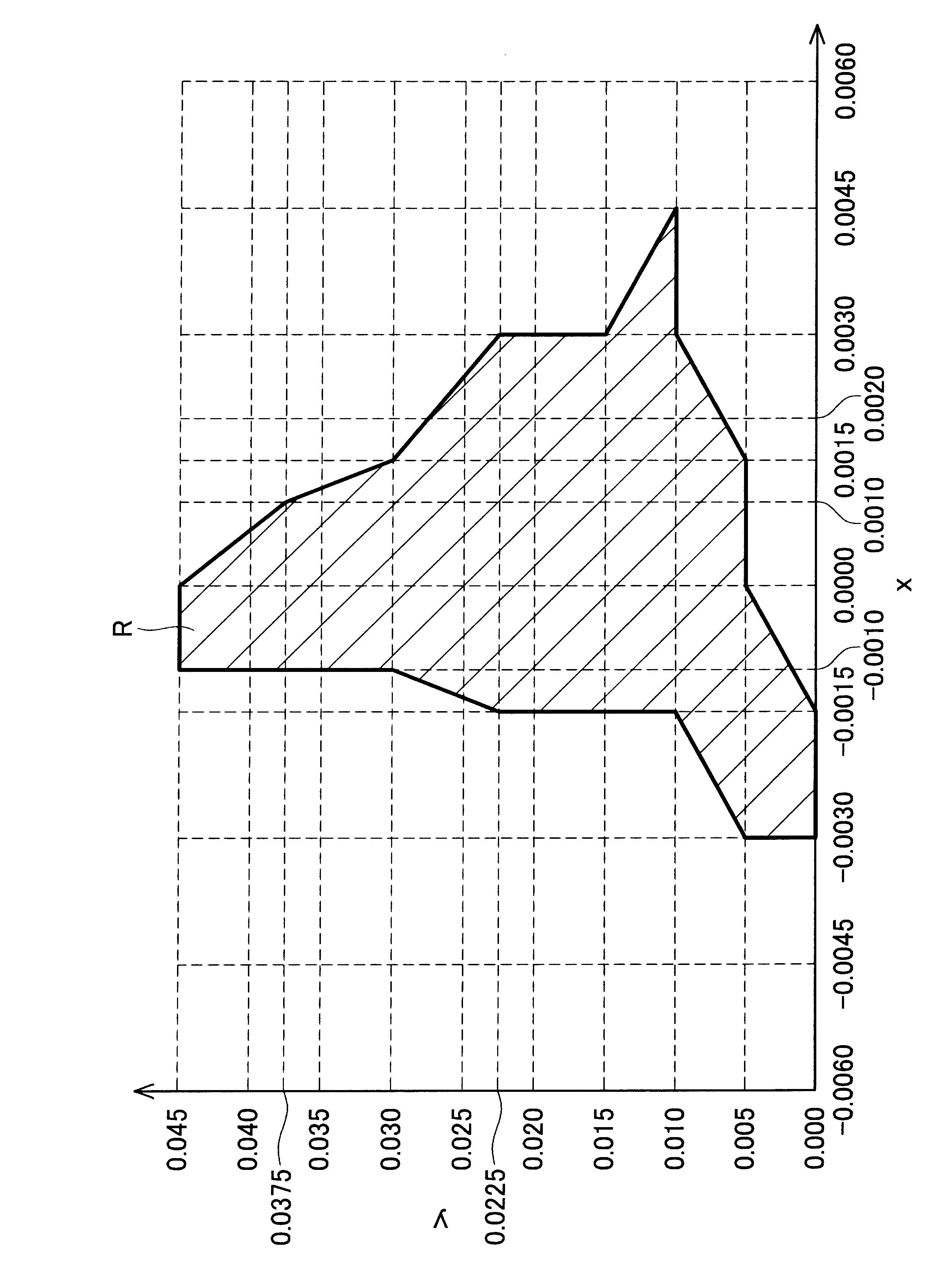
- the variable x is a value in the hatched region R and on the boundary line of the hatched region R shown in the following figure.
- the area / thickness ratio is a value obtained by dividing the area ( ⁇ m 2 ) of the piezoelectric substrate when the piezoelectric substrate is viewed in plan by the thickness ( ⁇ m) of the piezoelectric substrate.
- FIG. 1 shows the result of the experiment conducted by the inventors of the present invention superimposed on the above figure.
- ⁇ upward triangle
- ⁇ downward triangle
- ⁇ downward triangle
- atom diffusion from the piezoelectric substrate to the setter occurs.
- the ⁇ black dots
- the variable x and y if the value of the boundary line of the hatched regions R within and shaded area R, without sticking problems and diffusion problems, the thickness of not more than the piezoelectric substrate 30 ⁇ m preferred Can be manufactured.
- a piezoelectric substrate with a thickness of 30 ⁇ m or less can be suitably manufactured if the value is on the line. According to the above invention, a piezoelectric substrate of 30 ⁇ m or less can be manufactured.
- the setter is made of stabilized zirconia having a purity of 99.9 mol% or more, the weight concentration of Na in the setter is 50 ppm or less, and the weight concentration of Si in the setter is 5 ppm or more, And it is preferable that it is 50 ppm or less.
- Stabilized zirconia is a composition obtained by adding 5 to 10 mol% Y 2 O 3 to ZrO 2 .
- FIG. 1 The figure which shows the evaluation result of the piezoelectric material board manufactured with the manufacturing method of an Example.
- the flowchart which shows the manufacturing method which concerns on one Embodiment of this invention.
- FIG. The top view which shows arrangement
- FIG. 2 shows a manufacturing method according to an embodiment of the present invention.
- a piezoelectric substrate having a thickness of 30 ⁇ m or less can be manufactured.
- the ratio S / T between the thickness T ( ⁇ m) of the piezoelectric substrate to be manufactured and the area S ( ⁇ m 2 ) of the piezoelectric substrate can be 1 ⁇ 10 7 ( ⁇ m) or more.
- the area S of the piezoelectric substrate is an area of the piezoelectric substrate when the piezoelectric substrate is viewed in plan along the thickness direction of the piezoelectric substrate. In the manufacturing method shown in FIG. 2, such a PZT piezoelectric substrate can be preferably manufactured.
- a piezoelectric powder (that is, a powder having a composition that becomes a piezoelectric body when sintered) is synthesized.
- a piezoelectric powder can be synthesized by mixing various material powders and heating the mixed material powders.
- each of material powders composed of PbO, SrCO 3 , TiO 2 , ZrO 2 , Nb 2 O 5 is finely wet pulverized by a ball mill, a bead mill, etc. Uniform and disperse the particle size of the powder.
- each material powder is dried, and then each material powder is mixed using a dry crusher such as an atomizer.
- Step S2 is performed by adjusting the blending ratio of each material powder so that the synthesized piezoelectric powder has a composition of M 1 ⁇ y / 2 + x (N 1 ⁇ y Nb y ) O 3 + x .
- M represents Pb 1-p Sr p and N represents Ti 1-q Zr q .
- the variable p is adjusted to a value in the range of 0 ⁇ p ⁇ 0.03.
- the reason for adjusting the variable p within the range of 0 ⁇ p ⁇ 0.03 is that when the variable p exceeds 0.03, oxygen defects in the piezoelectric body increase, resulting in coarsening of the particle size and deterioration of the characteristics. It is.
- the variable q is adjusted to a value within the range of 0.45 ⁇ q ⁇ 0.60.
- the reason why the variable q is adjusted to a value of 0.45 or more is to prevent the grain size of the piezoelectric body from becoming coarse.
- the reason why the variable q is adjusted to a value of 0.60 or less is to prevent the decomposition of PbO during firing and to form a piezoelectric body having a perovskite structure.
- the variable q is preferably 0.51 ⁇ q ⁇ 0.55. According to such a configuration, since the sintered piezoelectric body has a composition in the vicinity of MPB (morphotopic phase), a piezoelectric substrate having a high piezoelectric constant can be manufactured. More preferably, 0.51 ⁇ q ⁇ 0.53. According to such a configuration, the fired piezoelectric body becomes tetragonal, and the amount of electric field induced strain of the piezoelectric substrate becomes larger when a high electric field is applied. Since a high electric field can be easily applied to a thin piezoelectric substrate having a thickness of 30 ⁇ m or less, it is desirable that the amount of electric field induced strain be large when a high electric field is applied.
- variables q are suitable when attention is paid to the amount of electric field induced strain when a high electric field is applied.
- the variable q satisfies at least the condition of 0.45 ⁇ q ⁇ 0.60. Just do it.
- This composition is obtained by adding Sr, Nb and PbO to Pb (Ti 1-q Zr q ) O 3 which is a general PZT composition.
- the variable x represents the addition amount of PbO
- the variable y represents the addition amount of Nb.
- M in the composition formula can also be represented as (Pb 1-p Sr p ) 1-y / 2 + x ⁇ y / 2 .
- the variables x and y are adjusted so as to have values in the hatched region R and the boundary of the hatched region R shown in FIG.
- a green sheet is formed using the piezoelectric powder synthesized in step S2.
- a green sheet can be formed by the following procedure. That is, a solvent, a dispersion material, a binder, and a plasticizer are added to the synthesized piezoelectric powder, and wet mixing is performed using a ball mill, a bead mill, or the like. Next, the mixed material is applied onto a PET film by a doctor blade method to form a green sheet. At this time, the thickness of the green sheet is set to 38 ⁇ m or less. Thus, when the thickness of the green sheet is 38 ⁇ m or less, the thickness of the piezoelectric substrate obtained after firing is 30 ⁇ m or less.
- step S6 the green sheet formed in step S4 is cut.
- the green sheet can be cut into a square having a side of about 40 mm.
- a known method can be used for cutting the green sheet.
- what is necessary is just to cut a green sheet with PET film, when the material mixed on PET film was apply
- step S8 the green sheet is degreased.
- the degreasing of the green sheet can be performed, for example, by the following procedure. That is, first, a green sheet is placed on a setter made of stabilized zirconia having a purity of 99.9% or more. Next, a porous setter is placed on the green sheet. That is, the green sheet is sandwiched between two setters. In this state, the green sheet is heated to 500 ° C. in an air ventilation atmosphere. Thereby, the green sheet can be degreased. Thus, if the green sheet is degreased with the porous setter placed thereon, it is possible to prevent the warpage of the green sheet during degreasing.
- the setter placed on the green sheet is porous, the gas generated from the green sheet at the time of degreasing is released to the outside through the pores inside the porous setter. Therefore, it can degrease suitably.
- a green sheet may break if a porous setter is too heavy, it is preferable to use a porous setter having an appropriate weight.
- what is necessary is just to remove the porous setter mounted on the green sheet after degreasing
- the steps S2 to S8 described above correspond to a step of forming a material having a composition of M 1-y / 2 + x (N 1-y Nb y ) O 3 + x into a sheet shape.
- step S10 the piezoelectric substrate is baked by heating the degreased green sheet. That is, the piezoelectric powder in the green sheet is sintered to be converted into ceramics, thereby obtaining a plate-like piezoelectric substrate.
- the firing of the piezoelectric substrate can be performed, for example, by the following procedure. That is, first, as shown in FIG. 3, a plurality of stabilized zirconia setters 20 that have been degreased are stacked in the sheath 40 with the green sheet 10 placed on the inside of the MgO sheath 40. To do. Note that four spacers 30 are arranged on the setter 20 as shown in FIG. 4, and a space is secured between the green sheet 10 and the setter 20 thereabove as shown in FIG.
- a dummy sheet 22 created by the same process as the green sheet 10 can be arranged around the green sheet 10.
- the dummy sheet 22 preferably has the same composition as the green sheet 10.
- the atmosphere powder (powder for adjusting the atmosphere inside the sheath at the time of firing) is placed inside the sheath in a state where it is placed in a MgO dish (not shown). In this state, the sheath is sealed and the inside of the sheath is heated. Thereby, the piezoelectric powder in the green sheet is sintered, and a plate-like piezoelectric substrate is completed. Note that the thickness of the green sheet decreases during firing.
- the thickness of the green sheet before firing is 38 ⁇ m or less, the thickness of the piezoelectric substrate after firing is 30 ⁇ m or less. Further, the green sheet before firing is a square having a side of about 40 mm, but this size is also reduced during firing.
- the fired piezoelectric substrate has a square shape with a side of about 32 mm. Therefore, the area / thickness ratio of the fired piezoelectric substrate is about 3 ⁇ 10 7 ⁇ m (that is, 1 ⁇ 10 7 ⁇ m or more).
- the firing temperature is not particularly limited, but can be appropriately set depending on the composition and particle diameter of the piezoelectric powder, the denseness required for the fired piezoelectric substrate, and the like.
- a dense piezoelectric substrate having the above composition and having a theoretical density of 95% or more is produced, it can be fired in the range of 1175 ° C. to 1250 ° C.
- the temperature is lower than 1175 ° C., the denseness is inferior, and when fired at 1250 ° C. or higher, the particles may grow abnormally or the decomposition of Pb cannot be suppressed, and a different phase may precipitate.
- the concentration of PbO gas around the green sheet 10 can be increased during firing. Thereby, the PbO is prevented from coming off from the green sheet 10, and the warpage of the green sheet 10 can be suppressed.
- the distance H1 between the setters 20 shown in FIG. 3 is preferably 30 ⁇ m or more and 200 ⁇ m or less, more preferably 50 ⁇ m or more and 150 ⁇ m or less.
- the thickness D1 of the uppermost setter 20a and the thickness D2 of the lowermost setter 20b are preferably at least twice the thickness D3 of the other setters 20. If a thick and heavy setter 20a is arranged at the top, the lower setter 20 can be pressed by the load of the setter 20a. Thereby, the warp of each setter 20 at the time of firing can be prevented. Further, by increasing the thickness of the lowermost setter 20b, the load of each upper setter 20 can be received without deformation of the setter 20b. By suppressing the warpage of each setter 20 as described above, the warpage of the green sheet 10 can be suppressed.
- the center line average roughness Ra indicating the surface roughness of the upper surface of the setter 20 is preferably 0.02 ⁇ m to 5 ⁇ m, and the maximum height Rmax is preferably 10 ⁇ m or less.
- the surface roughness of the setter 20 can be set to an appropriate value.
- the upper surface of the setter 20 is formed by polishing or blasting, it is difficult to reduce the maximum height Rmax, which is not preferable.
- the amount of impurities contained in the setter 20 it is preferable that Na is 50 ppm or less and Si is 50 ppm or less. This is because when there is too much Na or Si, mutual diffusion is easily placed between the setter 20 and the green sheet 10. Moreover, it is preferable that Si contained in the setter 20 is 5 ppm or more. This is because if the amount of Si is too small, the density of the setter 20 becomes low, and PbO enters the setter 20 and the PbO gas concentration in the atmosphere easily changes.
- a piezoelectric substrate having the following composition can be preferably manufactured. That is, according to this manufacturing method, it is possible to prevent atoms from diffusing from the piezoelectric substrate (that is, the green sheet) to the setter during firing while preventing the piezoelectric substrate and the setter from sticking. Thereby, the uniformity of the composition in the piezoelectric substrate can be ensured. In addition, since diffusion of atoms can be prevented in this way, a piezoelectric substrate having no difference in particle diameter between the front side surface and the back side surface can be manufactured.
- the surface of the piezoelectric substrate means the surface that was not in contact with the setter at the time of firing (ie, the upper surface), and the back surface of the piezoelectric substrate was the surface that was in contact with the setter at the time of firing (ie, the lower surface). means. More specifically, according to this production method, the difference in the average particle diameter between the front side surface and the back side surface is within 10% of the average value of the front side surface, and between the front side surface and the back side surface. Piezoelectric substrates in which the difference in the standard deviation of the particle diameter is within 10% of the standard deviation on the front side surface can be manufactured.
- the piezoelectric substrate manufactured using this method can then be used as a piezoelectric element by forming electrodes on both sides and cutting it into a predetermined shape.
- the piezoelectric element can be used as a piezoelectric actuator, a sensor, an ultrasonic motor, or the like by bonding to a circuit board so that a voltage can be applied between electrodes formed on both sides.
- a piezoelectric element manufactured from this piezoelectric substrate is preferably used in fields where downsizing and a large amount of displacement are required. be able to.
- a large piezoelectric substrate can be manufactured, so that a large number of piezoelectric elements can be obtained, and the piezoelectric elements can be manufactured at low cost.
- a piezoelectric substrate having a thickness of 30 ⁇ m or less can be manufactured by firing. That is, a thin piezoelectric substrate can be obtained without performing surface polishing or the like (that is, thinning) of the piezoelectric substrate after firing. Therefore, this manufacturing method can manufacture a thin piezoelectric substrate with excellent production efficiency.
- both the front side surface and the back side surface are fired surfaces (surfaces exposed to the surface of the piezoelectric substrate during firing). On the fired surface, there are minute irregularities due to the particle diameter of the piezoelectric body constituting the piezoelectric substrate. For this reason, when the electrode is formed on the surface of the piezoelectric substrate, the adhesion of the electrode to the piezoelectric substrate is high.
- the manufacturing method mentioned above was used for the manufacturing method.
- the manufactured piezoelectric substrate had a square shape of about 40 mm and a thickness of about 15 ⁇ m.
- FIG. 5 shows the result of evaluating the adhesion and c / a front / back difference for each piezoelectric substrate.
- the sticking in FIG. 5 means that the piezoelectric substrate sticks to the setter during firing in step S10.
- the presence or absence of sticking was determined by checking whether or not the piezoelectric substrate was moved after firing in step S10. O of the evaluation result of sticking represents that no sticking occurred in all of the ten test sheets, and X represents that sticking occurred even in one sheet.
- the c / a front / back difference means the difference in c / a between the front and back sides of the piezoelectric substrate.
- c / a is a axial ratio tetragonal a crystal lattice of the piezoelectric (value obtained by dividing the length c of the shaft which does not form a square with length a of the shaft constituting the square).
- O in the evaluation result of c / a front / back difference means that the c / a front / back difference is 0.001 or less, and X means that the c / a front / back difference is larger than 0.001.
- the measurement error of c / a is about 0.001
- c / a was calculated from the ratio of the detected intensity of the (200) plane and the detected intensity of the (002) plane in X-ray diffraction.
- the X-ray diffractometer uses X-part MPD Pro made by Spectris, the X-ray source measures CuK ⁇ , acceleration voltage 45kV, and the range of 40 ° -50 ° by ⁇ / 2 ⁇ method, so that the accuracy is high. The measurement time was set so that the main peak was 100,000 counts or more.
- FIG. 1 is a graph showing the evaluation results of FIG.
- ⁇ upward triangle
- ⁇ downward triangle
- ⁇ black dot
- FIG. 1 shows that easily sticking occurs more variable x is smaller, but higher c / a front and back difference variable x is large there is a tendency becomes large, by the variable x with the appropriate value, these problems It turns out that it does not occur.
- the appropriate range of the variable x varies depending on the value of the variable y.
- the piezoelectric substrate can be suitably manufactured without causing the above.
- the variable p is in the range of 0 ⁇ p ⁇ 0.03, and the variable q is 0.
Landscapes
- Chemical & Material Sciences (AREA)
- Engineering & Computer Science (AREA)
- Ceramic Engineering (AREA)
- Manufacturing & Machinery (AREA)
- Materials Engineering (AREA)
- Structural Engineering (AREA)
- Organic Chemistry (AREA)
- Composite Materials (AREA)
- Inorganic Chemistry (AREA)
- Compositions Of Oxide Ceramics (AREA)
Abstract
圧電体基板の製造方法であって、M1-y/2+x(N1-yNby)O3+x(但し、0≦y≦0.045であり、MはPb1-pSrpを表し、0≦p≦0.03であり、NはTi1-qZrqを表し、0.45≦q≦0.60である)の組成を有する材料をシート形状に成形する工程と、シート形状に成形した材料をセッター上に載置した状態で焼成することで、厚みが30μm以下であり、面積/厚み比が1×107μm以上となる圧電体基板を得る工程を有しており、変数xが、図1に示す斜線領域R内及び斜線領域Rの境界線上の値である。
Description
本出願は、2011年3月30日に出願された日本国特許出願第2011-076265号に基づく優先権を主張する。その出願の全ての内容はこの明細書中に参照により援用されている。
本明細書が開示する技術は、圧電体基板の製造方法に関する。
圧電体基板の製造方法として、種々の製造方法が提案されている。例えば、日本国公開特許公報2007-084357には、Caを添加したZrO2からなるセッターを用いて圧電体基板を焼成する技術が開示されている。
従来から薄い圧電体基板に対するニーズが高まっており、近年では厚みが30μm以下の圧電体基板が求められるようになってきている。しかしながら、厚みが30μm以下の圧電体基板の製造方法は、未だ確立されていなかった。したがって、本明細書では、厚みが30μm以下の圧電体基板を好適に製造することができる製造方法を提供する。
本願発明者らは、厚みが30μm以下の圧電体基板をセッター上で焼成しようとすると、以下の2つの問題が生じることを発見した。1つは、圧電体基板がセッターに固着してしまうことである。固着が生じると、セッター上から圧電体基板を移動させる際に、圧電体基板が割れてしまう。もう1つは、圧電体基板とセッターとの接触面において圧電体基板からセッターへの原子の拡散が生じ、圧電体の特性が不均一化する(圧電体基板の表面と裏面とで特性が異なってしまう)ことである。何れも現象も、圧電体の特性に大きな影響を及ぼすため、問題となる。30μmよりも厚い圧電体基板を焼成する際にはこれら2つの問題が生じない場合でも、同じ条件で30μm以下の圧電体基板を焼成するとこれら2つの問題が生じる。例えば、図6~8は、Pb1-y/2+x(N1-yNby)O3+x(但し、NはTi0.48Zr0.52)の組成を有するグリーンシートを焼成することによって、圧電体基板を種々の厚みで製造し、固着率とc/a表裏差(c/a表裏差が高いことは、圧電体基板からセッターへの原子の拡散が生じていることを意味する)を評価した結果を示している。図6~8のグラフAは固着率を表しており、グラフBはc/a表裏差を表している。図6はx=0.0045、y=0.020のときの評価結果を示しており、図7はx=-0.003、y=0.020のときの評価結果を示しており、図8はx=0.000、y=0.000のときの評価結果を示している。図6~図8の何れにおいても、圧電体基板の厚みが30μmより大きい場合には固着率とc/a表裏差は共に低い値となる。しかしながら、圧電体基板の厚みが30μm以下となると、図6、8ではc/a表裏差が上昇し、図7では固着率が上昇する。このように、固着及び拡散の問題は、厚みが30μm以下の圧電体基板を焼成する際に初めて明らかになった問題である。本発明者らは、これらの問題の支配因子が圧電体材料の組成にあることを見出し、以下に開示する製造方法を想到するに至った。
本明細書が開示する圧電体基板の製造方法は、M1-y/2+x(N1-yNby)O3+x(但し、0≦y≦0.045であり、MはPb1-pSrpを表し、0≦p≦0.03であり、NはTi1-qZrqを表し、0.45≦q≦0.60である)の組成を有する材料をシート形状に成形する工程と、シート形状に成形した材料をセッター上に載置した状態で焼成することで、厚みが30μm以下であり、面積/厚み比が1×107μm以上となる圧電体基板を得る工程を有している。変数xは、以下の図に示す斜線領域R内及び斜線領域Rの境界線上の値である。
なお、面積/厚み比は、圧電体基板を平面視したときの圧電体基板の面積(μm2)を圧電体基板の厚み(μm)で除算した値である。
図1は、上記の図に、本願発明者が実施した実験結果を重ねて示している。図1において、△(上向き三角)は圧電体基板のセッターへの固着が発生したことを示しており、▽(下向き三角)は圧電体基板からセッターへの原子の拡散が発生したことを示しており、●(黒ドット)はこれらの何れもが発生しなかったこと(すなわち、圧電体基板を好適に製造することができたこと)を意味する。図示するように、変数x及びyが、斜線領域R内及び斜線領域Rの境界線上の値であれば、固着の問題及び拡散の問題が生じることなく、厚みが30μm以下の圧電体基板を好適に製造することができる。なお、0≦p≦0.03であり、0.45≦q≦0.60であれば、変数p及びqが何れの場合でも、変数x及びyが斜線領域R内及び斜線領域Rの境界線上の値であれば30μm以下の圧電体基板を好適に製造することができることが確認できた。上記の発明によれば、30μm以下の圧電体基板を製造することができる。
上述した製造方法は、セッターが、純度が99.9mol%以上の安定化ジルコニアにより構成されており、セッター中におけるNaの重量濃度が50ppm以下であり、セッター中におけるSiの重量濃度が5ppm以上、かつ、50ppm以下であることが好ましい。なお、安定化ジルコニアとは、ZrO2に5~10mol%のY2O3を添加した組成物である。
図2は、本発明の一実施形態に係る製造方法を示している。この製造方法では、厚みが30μm以下の圧電体基板を製造することができる。製造する圧電体基板の厚みT(μm)と圧電体基板の面積S(μm2)の比S/Tは、1×107(μm)以上とすることができる。なお、圧電体基板の面積Sは、圧電体基板の厚み方向に沿って圧電体基板を平面視したときの圧電体基板の面積である。図2に示す製造方法では、このようなPZTの圧電体基板を好適に製造することができる。
ステップS2では、圧電体粉末(すなわち、焼結させると圧電体となる組成を有する粉末)を合成する。例えば、種々の材料粉末を混合し、その混合した材料粉末を加熱することで圧電体粉末を合成することができる。具体的な実施形態としては、例えば、最初に、PbO、SrCO3、TiO2、ZrO2、Nb2O5により構成される材料粉末のそれぞれをボールミル、ビーズミル等によってより細かく湿式粉砕し、各材料粉末の粒径を均一化、分散させる。次に、各材料粉末を乾燥させ、その後、アトマイザ等の乾式解砕機を用いて各材料粉末を混合する。次に、混合した材料粉末を約950℃で仮焼(合成)する。このような手順によって、圧電体粉末を合成することができる。ステップS2は、合成した圧電体粉末が、M1-y/2+x(N1-yNby)O3+xの組成となるように、各材料粉末の配合比を調整して行う。なお、MはPb1-pSrpを表し、NはTi1-qZrqを表す。変数pは、0≦p≦0.03の範囲内の値に調節する。変数pを0≦p≦0.03の範囲内に調整するのは、変数pが0.03を超えると圧電体中の酸素欠陥が増加し、粒径の粗大化及び特性の低下を引き起こすためである。また、変数qは、0.45≦q≦0.60の範囲内の値に調節する。変数qを0.45以上の値にに調整するのは、圧電体の粒径が粗大化することを防ぐためである。また、変数qを0.60以下の値に調整するのは、焼成時におけるPbOの分解を防いで、ペロブスカイト構造の圧電体を形成するためである。なお、変数qは、0.51≦q≦0.55であることが好ましい。このような構成によれば、焼成後の圧電体がMPB(モルフォロトピック相)近傍の組成となるので、高い圧電定数を有する圧電体基板を製造することができる。より好ましくは、0.51≦q≦0.53であることが好ましい。このような構成によれば、焼成後の圧電体が正方晶となり、高電界印加時に圧電体基板の電界誘起歪量がより大きくなる。30μm以下の薄い圧電体基板では高電界を容易に印加することができるので、このように高電界印加時に電界誘起歪量が大きいことが望ましい。但し、これらの変数qの値は、高電界を印加した際の電界誘起歪量に着目したときに好適な値である。製造時におけるセッターへの固着、及び、セッターと圧電体基板との間の原子の拡散に着目した場合には、変数qについては、少なくとも0.45≦q≦0.60の条件が満たされていればよい。
ここで、変数x、yについて説明する。M1-y/2+x(N1-yNby)O3+x(但し、MはPb1-pSrpを表し、NはTi1-qZrqを表す。)の組成を有する圧電体は、ペロブスカイト構造を有する。この組成は、一般的なPZTの組成であるPb(Ti1-qZrq)O3に対して、Srと、Nbと、PbOを添加したものである。変数xはPbOの添加量を表し、変数yはNbの添加量を表している。なお、Mに-y/2の添え字が付いているのは、Nbが5価であるために、2価であるMのサイトに-y/2の欠陥が形成されるためである。欠陥をαで表すと、上記組成式中のMは、(Pb1-pSrp)1-y/2+xαy/2と表すこともできる。変数x、yは、後述するように、図1に示す斜線領域R内及び斜線領域Rの境界線上の値となるように調整される。
ステップS4では、ステップS2で合成した圧電体粉末を用いてグリーンシートを成形する。例えば、次の手順でグリーンシートを成形することができる。すなわち、合成した圧電体粉末に、溶剤、分散材、バインダー、及び、可塑剤を加え、ボールミル、ビーズミル等を用いて湿式混合する。次に、混合した材料をドクターブレード法によってPETフィルム上に塗布することで、グリーンシートを成形する。このとき、グリーンシートの厚みを38μm以下とする。このように、グリーンシートの厚みを38μm以下とすると、焼成後に得られる圧電体基板の厚みが30μm以下となる。
ステップS6では、ステップS4で成形したグリーンシートをカットする。例えば、一辺が約40mmの正方形にグリーンシートをカットすることができる。グリーンシートのカットには、公知の方法を用いることができる。なお、グリーンシート成形時に、上記のようにPETフィルム上に混合した材料を塗布していた場合は、PETフィルムと共にグリーンシートをカットすればよい。そして、カット後に、グリーンシートをPETフィルムから剥離すればよい。
ステップS8では、グリーンシートを脱脂する。グリーンシートの脱脂は、例えば、次の手順で行うことができる。すなわち、最初に、99.9%以上の純度の安定化ジルコニアにより構成されたセッター上にグリーンシートを載せる。次に、グリーンシート上に多孔質のセッターを載せる。すなわち、グリーンシートを2つのセッターで挟み込む。この状態で、大気通風雰囲気中で、グリーンシートを500℃に加熱する。これによって、グリーンシートを脱脂することができる。このように、多孔質セッターを載せた状態でグリーンシートを脱脂すると、脱脂時にグリーンシートに反りが発生することを防止することができる。また、グリーンシートに載せるセッターが多孔質であるので、脱脂時にグリーンシートから生じるガスは、多孔質セッターの内部の空孔を通って外部に放出される。したがって、好適に脱脂することができる。なお、多孔質セッターが重すぎるとグリーンシートが割れることがあるので、適切な重さの多孔質セッターを用いることが好ましい。なお、多孔質セッターを載せた状態で脱脂した場合は、脱脂後にグリーンシートに載せた多孔質セッターを取り外せばよい。以上に説明したステップS2~S8の工程は、M1-y/2+x(N1-yNby)O3+xの組成を有する材料をシート形状に成形する工程に相当する。
ステップS10では、脱脂したグリーンシートを加熱することで、圧電体基板を焼成する。すなわち、グリーンシート中の圧電体粉末を焼結させてセラミックス化することで、板状の圧電体基板を得る。圧電体基板の焼成は、例えば、次の手順で行うことができる。すなわち、まず、図3に示すように、MgO製の鞘40の内部に、脱脂工程を終えた複数の安定化ジルコニアのセッター20を、グリーンシート10を載せたままの状態で鞘40内に積層する。なお、セッター20上には図4に示すように4つのスペーサ30を配置して、図3に示すようにグリーンシート10とその上方のセッター20の間に空間を確保する。また、図4に示すように、セッター20上には、グリーンシート10に加えて、グリーンシート10と同様の工程により作成されたダミーシート22をグリーンシート10の周囲に配置することができる。ダミーシート22は、グリーンシート10と同じ組成を有することが好ましい。次に、鞘の内部に、雰囲気粉(焼成時における鞘の内部の雰囲気を調節するための粉)をMgO製の皿に入れた状態で配置する(図示省略)。この状態で、鞘を密閉し、鞘の内部を加熱する。これによって、グリーンシート中の圧電体粉末が焼結し、板状の圧電体基板が完成する。なお、焼成時にグリーンシートの厚みが減少する。焼成前のグリーンシートの厚みが38μm以下であるので、焼成後の圧電体基板の厚みは30μm以下となる。また、焼成前のグリーンシートは一辺が約40mmの正方形であるが、焼成時にこのサイズも縮小する。焼成後の圧電体基板は、一辺が約32mmの正方形となる。したがって、焼成後の圧電体基板の面積/厚み比は、約3×107μm(すなわち、1×107μm以上)となる。なお、焼成温度は、特に限定されないが、圧電体粉末の組成と粒子径や焼成後の圧電体基板に求める緻密性等によって適宜設定することができる。例えば、上記の組成で理論密度の95%以上である緻密な圧電体基板を製造するのであれば、1175℃~1250℃の範囲で焼成することができる。1175℃を下回ると緻密性が劣り、1250℃以上で焼成すると粒子が異常成長したり、Pbの分解を抑えることができず、異相が析出することがある。
なお、上記のようにグリーンシート10の周囲にグリーンシート10と同じ組成のダミーシート22を配置すると、焼成時にグリーンシート10の周囲のPbOガスの濃度を高めることができる。これによって、グリーンシート10からPbOが抜けることが抑制され、グリーンシート10の反りを抑制することができる。
また、図3に示すセッター20の間の間隔H1が狭すぎると、焼成時にセッター20に反りが生じたときに、グリーンシート10が上部のセッター20に接触し、グリーンシート10が変形する。また、間隔H1が広すぎると、グリーンシート10上の空間が広くなり、グリーンシート10の周囲のPbOガス濃度が安定しなくなるので、グリーンシート10に反りが発生する。したがって、2つのセッター20の間の間隔H1は、30μm以上であり200μm以下であることが好ましく、50μm以上であり150μm以下であることがより好ましい。
また、図3に示すように、最上部のセッター20aの厚みD1と最下部のセッター20bの厚みD2は、これら以外のセッター20の厚みD3の2倍以上であることが好ましい。最上部に厚く重いセッター20aを配置しておくと、セッター20aの荷重によってその下部のセッター20を押さえつけることができる。これによって、焼成時における各セッター20の反りを防止することができる。また、最下部のセッター20bを厚くすることで、セッター20bが変形することなく上部の各セッター20の荷重を受けることができる。これらのように各セッター20の反りを抑制することで、グリーンシート10の反りを抑制することができる。
また、上記の製造方法においては、セッター20の上面の表面粗さを示す中心線平均粗さRaが0.02μm~5μmであり、最大高さRmaxが10μm以下であることが好ましい。このためには、粒径が0.5μm~1.5μmのZrO2の材料粉末を用いてシートを形成し、そのシートを焼成することでセッター20を形成することが好ましい。このようにセッター20を形成することで、セッター20の表面粗さを適切な値とすることができる。セッター20の上面を研磨やブラスト加工で成形する場合には、最大高さRmaxを小さくすることが困難であり、好ましくない。また、セッター20に含まれる不純物量は、Naが50ppm以下であり、Siが50ppm以下であることが好ましい。NaやSiが多すぎると、セッター20とグリーンシート10との間で相互拡散が置き易いためである。また、セッター20に含まれるSiは5ppm以上であることが好ましい。Siが少なすぎると、セッター20の緻密性が低くなり、セッター20中にPbOが入り込んで雰囲気中のPbOガス濃度が変化し易いためである。
上記の製造方法によれば、M1-y/2+x(N1-yNby)O3+x(但し、MはPb1-pSrpを表し、NはTi1-qZrqを表す。)の組成を有する圧電体基板を好適に製造することができる。すなわち、この製造方法によれば、圧電体基板とセッターとの固着を防止しつつ、かつ、焼成時に圧電体基板(すなわち、グリーンシート)からセッターに原子が拡散することを防止することができる。これによって、圧電体基板中における組成の均一性を確保することができる。また、このように原子の拡散を防止できるので、表側面と裏側面との間で粒子径に差がない圧電体基板を製造することができる。なお、圧電体基板の表面は、焼成時にセッターと接触していなかった面(すなわち、上面)を意味し、圧電体基板の裏面は、焼成時にセッターと接触していた面(すなわち、下面)を意味する。より具体的には、この製造方法によれば、表側面と裏側面との間における粒子径の平均値の差が表側面の平均値の10%以内であり、表側面と裏側面との間における粒子径の標準偏差の差が表側面の標準偏差の10%以内である圧電体基板)を製造することができる。本方法を用いて製造された圧電体基板は、その後、両面に電極を形成し、所定の形状に切断することで、圧電素子として用いることができる。さらに、両面に形成した電極間に電圧を印加できるよう、回路基板と接合することで、圧電素子を圧電アクチュエータ、センサ、超音波モータ等として用いることができる。特に、このように薄い圧電体基板には高電界を印加可能であることから、この圧電体基板から製造される圧電素子は、小型化、及び、大きな変位量が要求される分野で好適に用いることができる。また、この製造方法によれば大きな圧電体基板を製造することが可能であるので、圧電素子の多数個取りが可能であり、圧電素子を低コストで製造することが可能となる。
また、上記の方法によれば、焼成により厚みが30μm以下の圧電体基板を製造することができる。すなわち、焼成後に、圧電体基板の表面研磨等(すなわち、薄型化)を行うことなく、薄い圧電体基板を得ることができる。したがって、この製造方法は、優れた生産効率で薄い圧電体基板を製造することができる。また、このように製造された圧電体基板においては、その表側面と裏側面の両方が焼成面(焼成時に圧電体基板の表面に露出している面)である。焼成面には、圧電体基板を構成している圧電体の粒子径に起因する微小な凹凸が存在している。このため、圧電体基板の表面に電極を形成する際に、圧電体基板に対する電極の密着性が高い。
以下、本発明を具現化した実施例について説明する。なお、以下の実施例は、本発明を説明するための具体例であって、本発明を限定するものではない。
変数x、yとして種々の値を採用して圧電体粉末を合成し、その合成した圧電体粉末を1200℃で3時間焼成して圧電体基板を製造した。製造方法には、上述した製造方法を用いた。製造された圧電体基板は、約40mmの正方形状を有し、その厚みは約15μmであった。製造した全ての圧電体基板において、q=0.525とし、p=0.02とした。なお、q=0.525である場合には、圧電体の結晶格子は正方晶となる。
製造した圧電体基板のそれぞれについて、固着とc/a表裏差を評価した。図5は、各圧電体基板について固着とc/a表裏差を評価した結果を示している。図5における固着とは、ステップS10の焼成時に圧電体基板がセッターに固着することを意味している。固着の有無は、ステップS10の焼成後に、圧電体基板を押して動くかどうかを確認することで判断した。固着の評価結果のOは試験数10シートに対し、全てにおいて固着が生じなかったことを表し、Xは1シートでも固着が生じたことを表す。
また、c/a表裏差とは、圧電体基板の表側面と裏側面との間におけるc/aの差を意味している。c/aは、圧電体の結晶格子である正方晶の軸比(正方形を構成する軸の長さaで正方形を構成しない軸の長さcを除算した値)である。図5の評価では、c/a表裏差が0.001より大きいか否か(すなわち、圧電体基板の表側面と裏側面の間でc/aに差があるか否か)を判断した。c/a表裏差の評価結果のOはc/a表裏差が0.001以下であったことを意味し、Xはc/a表裏差が0.001より大きかったことを意味する。なお、c/aの測定誤差は約0.001であるため、c/a表裏差が0.001以下であることは、測定可能な差が存在しないことを意味する。焼成時に圧電体基板からセッターにTiが拡散すると、圧電体基板の裏側部のc/aが変化する。したがって、この場合には、c/a表裏差が大きくなる。c/a表裏差が大きいと、表側面と裏側面の間で圧電定数が異なってしまい、電圧印加時に圧電体が反るように変形するため好ましくない。なお、c/aは、X線回折における(200)面の検出強度と(002)面の検出強度の比から算出した。X線回折装置は、スペクトリス社製X‘part MPD Proを用い、X線源はCuKα、加速電圧45kV、θ/2θ法で40°~50°の範囲を測定し、精度が高くなるように、メインピークが100000counts以上となるように測定時間を設定した。
図1は、図5の評価結果をグラフとして表したものである。図1において、△(上向き三角)は固着が発生したことを示しており、▽(下向き三角)はc/a表裏差が大きかったことを示し、●(黒ドット)はこれらの問題が生じなかったこと(すなわち、圧電体基板を好適に製造することができたこと)を意味する。図示するように、変数xが小さいほど固着が発生し易く、変数xが大きいほどc/a表裏差が大きくなり易い傾向があるが、変数xを適切な値とすることで、これらの問題が生じないことが分かる。変数xの適切な範囲は、変数yの値によって変化する。すなわち、変数yを0≦y≦0.045の値に調節し、変数xを図1の斜線領域Rに示す範囲内及びその境界線上の値に調節することで、固着やTiの拡散の問題が生じることなく好適に圧電体基板を製造できることが分かった。
なお、図1は、p=0.02とし、q=0.525としたときの結果を表しているが、変数pが0≦p≦0.03の範囲内にあり、変数qが0.45≦q≦0.60の範囲内にあれば、変数p及びqが何れの値であっても、変数xとyが斜線領域Rの範囲内にあれば好適に厚みが30μm以下の圧電体基板を製造することが可能であること(すなわち、固着の問題が生じず、かつ、結晶格子の軸比の変動が生じないこと)が分かった。
以上、本発明の具体例を詳細に説明したが、これらは例示にすぎず、特許請求の範囲を限定するものではない。特許請求の範囲に記載の技術には、以上に例示した具体例をさまざまに変形、変更したものが含まれる。
本明細書または図面に説明した技術要素は、単独であるいは各種の組み合わせによって技術的有用性を発揮するものであり、出願時請求項記載の組み合わせに限定されるものではない。また、本明細書または図面に例示した技術は複数目的を同時に達成するものであり、そのうちの一つの目的を達成すること自体で技術的有用性を持つものである。
本明細書または図面に説明した技術要素は、単独であるいは各種の組み合わせによって技術的有用性を発揮するものであり、出願時請求項記載の組み合わせに限定されるものではない。また、本明細書または図面に例示した技術は複数目的を同時に達成するものであり、そのうちの一つの目的を達成すること自体で技術的有用性を持つものである。
Claims (2)
- 圧電体基板の製造方法であって、
M1-y/2+x(N1-yNby)O3+x(但し、0≦y≦0.045であり、MはPb1-pSrpを表し、0≦p≦0.03であり、NはTi1-qZrqを表し、0.45≦q≦0.60である)の組成を有する材料をシート形状に成形する工程と、
シート形状に成形した材料をセッター上に載置した状態で焼成することで、厚みが30μm以下であり、面積/厚み比が1×107μm以上となる圧電体基板を得る工程を有しており、
変数xが、以下の図に示す斜線領域R内及び斜線領域Rの境界線上の値である、
ことを特徴とする方法。

- セッターが、純度が99.9mol%以上の安定化ジルコニアにより構成されており、
セッター中におけるNaの重量濃度が50ppm以下であり、セッター中におけるSiの重量濃度が5ppm以上、かつ、50ppm以下であることを特徴とする請求項1に記載の方法。
Priority Applications (2)
| Application Number | Priority Date | Filing Date | Title |
|---|---|---|---|
| JP2013507672A JP5847803B2 (ja) | 2011-03-30 | 2012-03-28 | 圧電体基板の製造方法 |
| US14/041,114 US9219224B2 (en) | 2011-03-30 | 2013-09-30 | Method for manufacturing piezoelectric substrate |
Applications Claiming Priority (2)
| Application Number | Priority Date | Filing Date | Title |
|---|---|---|---|
| JP2011076265 | 2011-03-30 | ||
| JP2011-076265 | 2011-03-30 |
Related Child Applications (1)
| Application Number | Title | Priority Date | Filing Date |
|---|---|---|---|
| US14/041,114 Continuation US9219224B2 (en) | 2011-03-30 | 2013-09-30 | Method for manufacturing piezoelectric substrate |
Publications (1)
| Publication Number | Publication Date |
|---|---|
| WO2012133529A1 true WO2012133529A1 (ja) | 2012-10-04 |
Family
ID=46931238
Family Applications (1)
| Application Number | Title | Priority Date | Filing Date |
|---|---|---|---|
| PCT/JP2012/058129 Ceased WO2012133529A1 (ja) | 2011-03-30 | 2012-03-28 | 圧電体基板の製造方法 |
Country Status (3)
| Country | Link |
|---|---|
| US (1) | US9219224B2 (ja) |
| JP (1) | JP5847803B2 (ja) |
| WO (1) | WO2012133529A1 (ja) |
Families Citing this family (3)
| Publication number | Priority date | Publication date | Assignee | Title |
|---|---|---|---|---|
| WO2016031994A1 (ja) | 2014-08-29 | 2016-03-03 | 京セラ株式会社 | 圧電磁器板および板状基体ならびに電子部品 |
| JP6629949B2 (ja) * | 2017-12-19 | 2020-01-15 | 三ツ星ベルト株式会社 | 伝動ベルト及び伝動ベルトの状態情報取得システム |
| US12121964B2 (en) | 2018-11-07 | 2024-10-22 | James J. Myrick | Processes, compositions and systems for 2D and 3D printing |
Citations (9)
| Publication number | Priority date | Publication date | Assignee | Title |
|---|---|---|---|---|
| JPH08178549A (ja) * | 1994-12-27 | 1996-07-12 | Ngk Insulators Ltd | 電子材料焼成用ジルコニア質セッター |
| JP2001272178A (ja) * | 2000-03-29 | 2001-10-05 | Toshiba Corp | 熱処理治具 |
| JP2006193415A (ja) * | 2004-12-17 | 2006-07-27 | Tdk Corp | 圧電磁器および圧電素子 |
| JP2010037121A (ja) * | 2008-08-04 | 2010-02-18 | Ngk Insulators Ltd | 焼成用セッター |
| JP2010093598A (ja) * | 2008-10-09 | 2010-04-22 | Murata Mfg Co Ltd | 圧電振動子およびその製造方法 |
| JP2011009269A (ja) * | 2009-06-23 | 2011-01-13 | Nippon Soken Inc | 圧電材料、積層型圧電素子及びその製造方法、ユニット接合積層型圧電素子 |
| JP2011011923A (ja) * | 2009-06-30 | 2011-01-20 | Taiheiyo Cement Corp | 圧電磁器組成物 |
| JP2011057550A (ja) * | 2001-09-29 | 2011-03-24 | Ceramtec Ag Innovative Ceramic Engineering | ペロフスカイト結晶構造を有するジルコンチタン酸鉛(pzt)を基礎とする圧電セラミック材料 |
| WO2011148969A1 (ja) * | 2010-05-26 | 2011-12-01 | 日本碍子株式会社 | 圧電素子の製造方法 |
Family Cites Families (15)
| Publication number | Priority date | Publication date | Assignee | Title |
|---|---|---|---|---|
| JP2737532B2 (ja) | 1991-07-23 | 1998-04-08 | 株式会社村田製作所 | 圧電磁器組成物 |
| JP3018683B2 (ja) | 1991-11-05 | 2000-03-13 | 株式会社村田製作所 | 鉛を含有するセラミックスの製造方法 |
| JP3119101B2 (ja) | 1994-11-28 | 2000-12-18 | 株式会社村田製作所 | 圧電磁器組成物 |
| JPH08283069A (ja) | 1995-04-07 | 1996-10-29 | Nippon Cement Co Ltd | 圧電セラミックス及びその製造方法 |
| JPH0971476A (ja) | 1995-09-08 | 1997-03-18 | Murata Mfg Co Ltd | セラミックの熱処理方法 |
| JP3087644B2 (ja) | 1996-03-26 | 2000-09-11 | 株式会社村田製作所 | 誘電体磁器組成物 |
| JP4752156B2 (ja) | 2001-08-23 | 2011-08-17 | 株式会社村田製作所 | 積層圧電素子用圧電磁器組成物、積層圧電素子、積層圧電素子の製造方法および積層圧電装置 |
| JP4432341B2 (ja) | 2003-03-24 | 2010-03-17 | Tdk株式会社 | セラミック板の焼成方法 |
| JP2005170769A (ja) | 2003-12-15 | 2005-06-30 | Tdk Corp | セラミック基板の製造方法 |
| JP4777605B2 (ja) * | 2003-05-21 | 2011-09-21 | 日本碍子株式会社 | 多層型圧電/電歪素子 |
| JP2005213117A (ja) | 2004-01-30 | 2005-08-11 | Tdk Corp | セラミック基板の製造方法 |
| JP4358777B2 (ja) | 2004-05-24 | 2009-11-04 | Tdk株式会社 | ジルコニアセッター及びセラミック基板の製造方法 |
| JP4782518B2 (ja) | 2005-09-20 | 2011-09-28 | 京セラ株式会社 | 鉛含有化合物の熱処理に用いられる部材 |
| JP4622887B2 (ja) | 2006-02-28 | 2011-02-02 | Tdk株式会社 | セラミック焼成体の製造方法 |
| EP1973177B8 (en) * | 2007-03-22 | 2015-01-21 | FUJIFILM Corporation | Ferroelectric film, process for producing the same, ferroelectric device, and liquid discharge device |
-
2012
- 2012-03-28 WO PCT/JP2012/058129 patent/WO2012133529A1/ja not_active Ceased
- 2012-03-28 JP JP2013507672A patent/JP5847803B2/ja not_active Expired - Fee Related
-
2013
- 2013-09-30 US US14/041,114 patent/US9219224B2/en not_active Expired - Fee Related
Patent Citations (9)
| Publication number | Priority date | Publication date | Assignee | Title |
|---|---|---|---|---|
| JPH08178549A (ja) * | 1994-12-27 | 1996-07-12 | Ngk Insulators Ltd | 電子材料焼成用ジルコニア質セッター |
| JP2001272178A (ja) * | 2000-03-29 | 2001-10-05 | Toshiba Corp | 熱処理治具 |
| JP2011057550A (ja) * | 2001-09-29 | 2011-03-24 | Ceramtec Ag Innovative Ceramic Engineering | ペロフスカイト結晶構造を有するジルコンチタン酸鉛(pzt)を基礎とする圧電セラミック材料 |
| JP2006193415A (ja) * | 2004-12-17 | 2006-07-27 | Tdk Corp | 圧電磁器および圧電素子 |
| JP2010037121A (ja) * | 2008-08-04 | 2010-02-18 | Ngk Insulators Ltd | 焼成用セッター |
| JP2010093598A (ja) * | 2008-10-09 | 2010-04-22 | Murata Mfg Co Ltd | 圧電振動子およびその製造方法 |
| JP2011009269A (ja) * | 2009-06-23 | 2011-01-13 | Nippon Soken Inc | 圧電材料、積層型圧電素子及びその製造方法、ユニット接合積層型圧電素子 |
| JP2011011923A (ja) * | 2009-06-30 | 2011-01-20 | Taiheiyo Cement Corp | 圧電磁器組成物 |
| WO2011148969A1 (ja) * | 2010-05-26 | 2011-12-01 | 日本碍子株式会社 | 圧電素子の製造方法 |
Also Published As
| Publication number | Publication date |
|---|---|
| US20140068904A1 (en) | 2014-03-13 |
| JPWO2012133529A1 (ja) | 2014-07-28 |
| US9219224B2 (en) | 2015-12-22 |
| JP5847803B2 (ja) | 2016-01-27 |
Similar Documents
| Publication | Publication Date | Title |
|---|---|---|
| EP2328193B1 (en) | Piezoelectric ceramic, method for making the same, piezoelectric element, liquid discharge head, and ultrasonic motor | |
| JP2010150126A (ja) | 圧電/電歪セラミックス組成物、圧電/電歪セラミックスの焼結体、圧電/電歪素子、圧電/電歪セラミックス組成物の製造方法及び圧電/電歪素子の製造方法 | |
| CN107235724B (zh) | 压电陶瓷溅射靶材、无铅压电薄膜以及压电薄膜元件 | |
| JP5021452B2 (ja) | 圧電/電歪磁器組成物および圧電/電歪素子 | |
| CN105658601B (zh) | 压电陶瓷及其制法、以及电子部件 | |
| US8277680B2 (en) | Method of manufacturing piezoelectric/electrostrictive ceramic composition | |
| US8084924B2 (en) | Piezoelectric/electrostrictive film element having wavy grain boundaries | |
| JP5847803B2 (ja) | 圧電体基板の製造方法 | |
| JP2017179415A (ja) | 圧電磁器スパッタリングターゲット、非鉛圧電薄膜およびそれを用いた圧電薄膜素子 | |
| JP5129067B2 (ja) | 圧電/電歪磁器組成物及び圧電/電歪素子 | |
| JP5597368B2 (ja) | 積層型電子部品およびその製法 | |
| JP5044437B2 (ja) | 圧電/電歪磁器焼結体の製造方法 | |
| WO2021010244A1 (ja) | 圧電体膜および圧電素子 | |
| CN113853692A (zh) | 压电陶瓷电子部件 | |
| JP5036758B2 (ja) | 圧電磁器およびそれを用いた圧電素子 | |
| US7125600B2 (en) | Setter, method for manufacturing ceramic substrate, and ceramic substrate | |
| JP6026530B2 (ja) | 圧電/電歪セラミックス組成物及び変位発生装置 | |
| JP5021595B2 (ja) | 圧電/電歪磁器組成物及び圧電/電歪素子 | |
| JP2017157829A (ja) | 板状基体および電子部品 | |
| JPH04325465A (ja) | 圧電セラミックスの焼成方法 | |
| JP2014209642A (ja) | 積層型電子部品およびその製法 | |
| JP2004010421A (ja) | 積層型セラミック焼成体の製造方法 |
Legal Events
| Date | Code | Title | Description |
|---|---|---|---|
| 121 | Ep: the epo has been informed by wipo that ep was designated in this application |
Ref document number: 12765355 Country of ref document: EP Kind code of ref document: A1 |
|
| ENP | Entry into the national phase |
Ref document number: 2013507672 Country of ref document: JP Kind code of ref document: A |
|
| NENP | Non-entry into the national phase |
Ref country code: DE |
|
| 122 | Ep: pct application non-entry in european phase |
Ref document number: 12765355 Country of ref document: EP Kind code of ref document: A1 |