WO2012128173A1 - 発光デバイス、及び該発光デバイスの製造方法 - Google Patents
発光デバイス、及び該発光デバイスの製造方法 Download PDFInfo
- Publication number
- WO2012128173A1 WO2012128173A1 PCT/JP2012/056681 JP2012056681W WO2012128173A1 WO 2012128173 A1 WO2012128173 A1 WO 2012128173A1 JP 2012056681 W JP2012056681 W JP 2012056681W WO 2012128173 A1 WO2012128173 A1 WO 2012128173A1
- Authority
- WO
- WIPO (PCT)
- Prior art keywords
- light emitting
- layer
- surfactant
- emitting device
- solution
- Prior art date
- Legal status (The legal status is an assumption and is not a legal conclusion. Google has not performed a legal analysis and makes no representation as to the accuracy of the status listed.)
- Ceased
Links
Images





Classifications
-
- B—PERFORMING OPERATIONS; TRANSPORTING
- B82—NANOTECHNOLOGY
- B82Y—SPECIFIC USES OR APPLICATIONS OF NANOSTRUCTURES; MEASUREMENT OR ANALYSIS OF NANOSTRUCTURES; MANUFACTURE OR TREATMENT OF NANOSTRUCTURES
- B82Y20/00—Nanooptics, e.g. quantum optics or photonic crystals
-
- C—CHEMISTRY; METALLURGY
- C09—DYES; PAINTS; POLISHES; NATURAL RESINS; ADHESIVES; COMPOSITIONS NOT OTHERWISE PROVIDED FOR; APPLICATIONS OF MATERIALS NOT OTHERWISE PROVIDED FOR
- C09K—MATERIALS FOR MISCELLANEOUS APPLICATIONS, NOT PROVIDED FOR ELSEWHERE
- C09K11/00—Luminescent materials, e.g. electroluminescent or chemiluminescent
- C09K11/02—Use of particular materials as binders, particle coatings or suspension media therefor
- C09K11/025—Use of particular materials as binders, particle coatings or suspension media therefor non-luminescent particle coatings or suspension media
-
- H—ELECTRICITY
- H10—SEMICONDUCTOR DEVICES; ELECTRIC SOLID-STATE DEVICES NOT OTHERWISE PROVIDED FOR
- H10K—ORGANIC ELECTRIC SOLID-STATE DEVICES
- H10K50/00—Organic light-emitting devices
- H10K50/10—OLEDs or polymer light-emitting diodes [PLED]
- H10K50/11—OLEDs or polymer light-emitting diodes [PLED] characterised by the electroluminescent [EL] layers
- H10K50/115—OLEDs or polymer light-emitting diodes [PLED] characterised by the electroluminescent [EL] layers comprising active inorganic nanostructures, e.g. luminescent quantum dots
Definitions
- Quantum dots which are nanoparticles with a particle size of 10 nm or less, have excellent carrier (electron, hole) confinement properties, and can easily generate excitons by electron-hole recombination. Therefore, light emission from free excitons can be expected, and light emission with high emission efficiency and sharp emission spectrum can be realized. Further, since quantum dots can be controlled in a wide wavelength range using the quantum size effect, their application to light emitting devices such as semiconductor lasers and light emitting diodes (LEDs) has attracted attention.
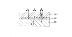
- FIG. 9 is a cross-sectional view schematically showing a quantum dot structure manufactured by a self-assembly method.
- a plurality of quantum dots 102 are discretely distributed on the surface of the first substrate 101, and a second substrate 103 is formed on the surface of the first substrate 101 so as to cover the quantum dots 102.
- distortion is caused by the difference between the lattice constant of the first substrate 101 and the lattice constant of the second substrate 103, and when the epitaxial growth cannot be performed, quantum dots 102 are formed at the locations where the distortion occurs. Is done.
- This self-assembly method is said to be capable of obtaining a high-quality quantum dot structure in which quantum dots are distributed at a higher density than in the case of artificially performing fine processing.
- the quantum dots 102 are discretely distributed on the first substrate 101, the quantum dots 102 cannot be integrated on the first substrate 101 with high density. That is, in this self-assembly method, the surface density of the quantum dots 102 is small, and the interval t between the quantum dots 102 tends to be larger than the quantum size of the quantum dots 102.
- the first substrate 101 is bonded to the second substrate 103 at locations other than where the quantum dots 102 are formed, electrons and holes are not injected into the quantum dots 102 but the first substrate 101 or the first substrate 101. 2 is transported to the second substrate 103, which may cause a decrease in luminous efficiency.
- carriers that are not injected into the quantum dots may be recombined outside the quantum dots 102. If the light is recombined outside the quantum dots 102 to emit light as described above, the emission color purity may be reduced. If the light is not emitted even after recombination, a leakage current may be caused and the emission efficiency may be reduced. There is.
- Patent Document 1 a substrate having a main surface made of a first semiconductor, a plurality of quantum dots distributed discretely on the main surface, and a surface on which the quantum dots are distributed is formed.
- a semiconductor device having a third semiconductor having a large band gap or a barrier layer formed of an insulating material has been proposed.
- a barrier layer 104 having an insulating property by oxidizing a semiconductor such as AlAs having a larger band gap energy than the first substrate 101 and the second substrate 103 is used.
- carriers electron and holes
- emission efficiency is improved by recombination.
- the quantum dot and the hole transport layer or the electron transport layer are in ohmic contact, the movement of the phonon is slow at the contact interface, and the high level is controlled by the slow movement of the phonon.
- the transition of the energy level from low to low is suppressed, and a phenomenon called a phonon bottleneck occurs.
- Patent Document 1 a first quantum well layer 105 and a first tunnel layer 106 are formed between the first substrate 101 and the barrier layer 104 as shown in FIG. A second tunnel layer 107 and a second quantum well layer 108 are formed between the layer 104 and the second substrate 103.
- Patent Document 1 in order to avoid a phonon bottleneck, the first and second quantum well layers 105 and 108 described above are formed, and carriers are transferred to the first and second quantum well layers 105 and 108.
- the confinement and the confined carriers are moved by the tunnel effect, thereby increasing the injection efficiency of the carriers into the quantum dots 102.
- Patent Document 2 discloses a light emitting layer that is formed of quantum dots and emits light by recombination of electrons and holes, an n-type inorganic semiconductor layer that transports the electrons to the light emitting layer, and the holes in the light emitting layer.
- a transporting p-type inorganic semiconductor layer, a first electrode for injecting the electrons into the n-type inorganic semiconductor layer, and a second electrode for injecting the holes into the p-type inorganic semiconductor layer There has been proposed a light emitting device comprising:
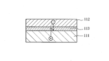
- Patent Document 2 As shown in FIG. 11, a p-type semiconductor layer 111 and an n-type semiconductor layer 112 are formed of an inorganic material, and a light-emitting layer and a p-type semiconductor layer 111 are formed between the p-type semiconductor layer 111 and the n-type semiconductor layer 112. A colloidal quantum dot layer 113 is interposed. That is, in Patent Document 2, a potential barrier is formed between the light-emitting layer and the carrier transport layer by forming the p-type semiconductor layer 111 and the n-type semiconductor layer 112 with an inorganic material having a band structure with good carrier transportability. Even if there is a carrier, carriers are injected into the colloidal quantum dot layer 113 by the tunnel effect, thereby improving the injection efficiency of carriers into the quantum dot layer 113.
- the colloidal quantum dot layer 113 is formed by immersing the board
- Patent Document 3 has a surfactant composed of at least two kinds of ligands localized on the surface of the quantum dot, and at least one of the ligands is a hole transporting ligand. There has been proposed a nanoparticle light-emitting material in which at least one kind is an electron transporting ligand.
- a surfactant having both a hole transporting ligand and an electron transporting ligand (hereinafter referred to as “amphoteric surfactant”) is used.
- the energy level is devised so as to produce a carrier blocking effect, and carriers are confined in the nanoparticles.
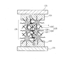
- FIG. 12 shows a case where Patent Document 3 is applied to a light emitting device.
- a light emitting layer 126 composed of an assembly of quantum dots 125 is interposed between a hole transport layer 122 formed on the upper surface of the anode 121 and an electron transport layer 124 formed on the lower surface of the cathode 123. Yes. And the surface of the quantum dot 125 is coat
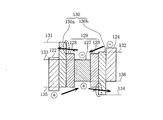
- FIG. 13 is a diagram for explaining the principle of confinement of quantum dots in Patent Document 3.
- the nanoparticle 129 includes the core portion 127 and the shell portion 128 that covers the core portion 127, and the shell portion 128 is covered with the amphoteric surfactant 130.
- This surfactant 130 has a hole-transporting ligand 130a and an electron-transporting ligand 130b, and the hole-transporting ligand 130a is localized on the hole transporting layer 122 side.
- the electron transporting ligand 130b is localized on the layer 124 side.
- the LUMO level 131 of the hole-transporting ligand 130a is set higher than the LUMO level 132 of the electron-transporting ligand 130b, whereby the electrons from the electron transport layer 124 are cored. While injecting into the portion 127, the LUMO level 131 of the hole transporting ligand 130 a is made higher than the lowest electron level 133 in the conduction band (where electrons move) of the core portion 127.
- the transporting ligand 130 a serves as a barrier against electrons, thereby confining the electrons inside the core portion 127.
- the LUMO level means that when a molecule is irradiated with light, the energy is in an excited state and the molecular orbitals are in an empty state not occupied by electrons. In this case, the molecular orbitals are not occupied by electrons.
- the energy level corresponding to the lowest lowest orbit (Lowest Unoccupied Molecular Orbital).
- the HOMO level means that in the ground state before the molecule is irradiated with light, electrons are occupied in order from the molecular orbital having the lowest energy. In this case, The energy level corresponding to the highest highest occupied orbital (Highest Occupied Molecular Orbital).
- the core portion 127 of the nanoparticle 129 is made to have carriers (electrons and holes) by the electron blocking effect of the hole transporting ligand 130a and the hole blocking effect of the electron transporting ligand 130b. Trapped inside.
- the electron-holes can be recombined in the core part 127, and exciton light can be emitted.
- the barrier layer 104 is formed after the quantum dot 102 is formed.
- the barrier layer on the quantum dot 102 is dry-etched so as not to prevent carrier injection into the quantum dot 102. 104 needs to be removed, resulting in a complicated manufacturing process.
- Patent Document 1 in order to avoid the occurrence of a phonon bottleneck, the first quantum well layer 105 and the first tunnel layer 106 are formed on the first substrate 101 as shown in FIG. In addition, the second tunnel layer 107 and the second quantum well layer 108 are formed on the surfaces of the quantum dot layer 102 and the barrier layer 104. Therefore, many film formation processes are required, which increases the cost. Invited and inferior in productivity.
- the quantum dots are not distributed in a discrete manner as in the self-assembly method, and surface defects can be improved while improving surface resistance by inactivating surface defects with a surfactant ligand. Is possible.
- the nanoparticle 129 is coated with the amphoteric surfactant 130 having both the hole transporting ligand 130 a and the electron transporting ligand 130 b, the holes and electrons are in the amphoteric surfactant 130. Will be transported in a coexisting form. For this reason, there is a possibility that electrons and holes approach each other with a certain probability, and holes and electrons may be recombined in the amphoteric surfactant 130 as shown by a in FIG.
- the light emitting layer 126 is formed only of an assembly of quantum dots 125 and the electron transport layer 124 is formed on the light emitting layer 126, as shown in FIG.
- the light emitting layer 126 may be filled with the electron transporting material 137.
- the size of the surfactant ligand is usually the same as the particle size of the nanoparticle 129, the carrier is not injected into the nanoparticle 129, but travels through the amphoteric surfactant 130 and passes through the quantum dot 125. May flow into the gap between the quantum dots 125 and the quantum dots 125.
- carriers may enter the hole transport layer 122 and the electron transport layer 124 without being injected into the nanoparticles 129.
- electrons may combine with holes to emit excitons. That is, in Patent Document 3, excitons do not emit light in the core portion 127 of the nanoparticle 129, and carriers that emit exciton are generated in the filled electron transporting material 137, and therefore, the emission efficiency decreases and the light emission occurs. There is a risk of lowering the color purity.
- the present invention has been made in view of such circumstances, and an object of the present invention is to provide a light-emitting device with good carrier injection efficiency into quantum dots and a method for manufacturing the light-emitting device.
- the present inventor conducted intensive research to achieve the above-mentioned object.
- the surface of the ultrafine particles was coated with two kinds of surfactants that transport only electrons or only holes, thereby forming quantum dots.
- the efficiency of carrier injection into ultrafine particles can be improved, thereby improving the light emission characteristics. I got the knowledge that I can do it.
- the light-emitting device is a light-emitting device in which a light-emitting layer is formed of an assembly of quantum dots, and the quantum dot has an ultrafine particle surface.
- the light emitting layer is coated with a first surfactant having a hole transporting property and a second surfactant having an electron transporting property, and the light emitting layer is an insulating material made of a polymer compound between the quantum dots. It is characterized by being filled.
- the first surfactant can transport only holes
- the second surfactant can transport only electrons
- the carriers are injected into the ultrafine particles with high efficiency. It can suppress passing outside.
- the polymer compound is selected from the group consisting of a polyimide resin, an acrylic resin, a polystyrene resin, a polycarbonate resin, a polyester resin, a polyamide resin, and a polyvinyl resin. Preferably it contains more than one species.
- a phonon bottleneck is generated by moving carriers between the first surfactant having electron transporting property and the second surfactant having hole transporting property and the quantum dot using tunnel resonance.
- the carrier can be transported quickly and efficiently.
- the first surfactant preferably has a HOMO level that causes tunnel resonance with the valence band of the quantum dot, and the second surfactant has a tunnel resonance with the conduction band of the quantum dot. It is preferable to have such a LUMO level.
- the first surfactant has a HOMO level that causes tunnel resonance with the valence band of the ultrafine particles.
- the HOMO level is preferably ⁇ 0.2 to +0.2 eV with respect to the energy level of the valence band.
- the first surfactant is ⁇ 0.2 to +0 with respect to the HOMO level that tunnels with the valence band of the quantum dot that is an ultrafine particle, for example, the energy level of the valence band.
- the HOMO level that tunnels with the valence band of the quantum dot that is an ultrafine particle, for example, the energy level of the valence band.
- the second surfactant has a LUMO level that causes tunnel resonance with the conduction band of the ultrafine particles.
- the LUMO level is preferably ⁇ 0.2 to +0.2 eV with respect to the energy level of the conduction band.
- the second surfactant has a LUMO level that causes tunnel resonance with the conduction band of the quantum dot that is the ultrafine particle, for example, ⁇ 0.2 to +0. By setting it to 2 eV, electrons move rapidly between the quantum dot and the surfactant by tunnel resonance.
- the ultrafine particles include any one of an oxide, a compound semiconductor, and a single semiconductor.
- the ultrafine particles have a core-shell structure including a core portion and a shell portion covering the core portion.
- a hole transport layer is formed on one main surface of the light emitting layer and an electron transport layer is formed on the other main surface of the light emitting layer.
- the light emitting layer can be manufactured inexpensively and efficiently without preparing a mixed solution in which a quantum dot dispersion solution and an insulating solution are mixed, without requiring a plurality of complicated film forming processes.
- FIG. 10 is a schematic diagram for explaining a carrier confinement principle in Patent Document 3.
- FIG. 10 is a schematic diagram for explaining the problem of Patent Document 3.
- the core material for forming the core portion 10 is not particularly limited as long as it is a semiconductor material having a photoelectric conversion effect, and InP, CdSe, CdS, PbSe, or the like can be used.
- the ligand is not particularly limited as long as it is a polar group.
- thiol group —SH
- amino group —NH 2
- carboxyl group —COOH
- carbonyl group —CO
- a nitro group —NO 2
- a phosphino group —PH 2
- a phosphoroso group —PO
- a polymer material such as poly (3,4-ethylenedioxythiophene): poly (styrenesulfonate) (hereinafter referred to as “PEDOT: PSS”) is preferably used as the material for the hole transport layer. Although it can be used, it is not preferable to use it as a material for a hole transporting surfactant. Since the polymer material has a large molecular size, which becomes a steric hindrance, the adjacent distance cannot be shortened. As a result, the surface coverage of the nanoparticles 9 decreases, leading to a decrease in quantum yield, The surface density of the quantum dots 5 cannot be increased.
- Such an insulating material is preferably a polymer compound.
- a crystal grain boundary is formed, so that the carrier is not injected into the core part 10 of the nanoparticle 9 and passes around the nanoparticle 9 in such a form as to propagate through the crystal grain boundary, Alternatively, electrons and holes may recombine at the grain boundary, which is not preferable.
- holes and electrons do not flow into the gaps of the quantum dots 5, but are separated through the hole transporting surfactant 12 and the electron transporting surfactant 13 through different paths. Since they are transported inside the particles 9, the holes and electrons do not approach and recombine during transport, and can be transported efficiently even with a relatively thick film thickness of 10 ⁇ m level. Thus, photoelectric conversion from an electrical signal to an optical signal can be performed with high efficiency.
- FIG. 3 is a diagram showing the relationship between the energy levels of the surfactants 12 and 13 and the energy levels of the quantized carriers of the nanoparticles 9.
- FIG. 5 is a production process diagram showing a procedure for producing a quantum dot dispersion solution.
- an InP quantum dot solution adjusted to a predetermined temperature (for example, 150 ° C.), heated and cooled, and washed to remove excess organic components in the solution.
- a surfactant made of an organic compound such as hexadecylamine hereinafter referred to as “HDA”
- HDA hexadecylamine
- An InP / ZnS dispersion solution with / nZS as nanoparticles 9, that is, a raw material solution 19 is prepared.
- the raw material solution 19 and the surfactant solution 20 are mixed so that the surfactant solution 20 has a mixing ratio of about twice that of the raw material solution 19 to perform ligand substitution.
- ligand substitution is performed to form nanoparticles 9 as a hole transporting surfactant 12 having a hole transporting ligand and an electron having an electron transporting ligand.
- It coat covers with the transportable surfactant 12, and it enables it to transport only an electron or only a hole efficiently, and aims at the injection efficiency improvement of the carrier to the nanoparticle 9.
- the quantum dot dispersion solution 22 and the insulating solution 23 are mixed to produce a mixed solution 24 as shown in FIG.
- a polystyrene resin is used for the insulating material 14
- acetone, methanol, ethanol or the like can be used in addition to the aromatic hydrocarbon and chlorine-containing hydrocarbon described above.
- phenol and methanol can be used.
- aniline and pyridine can be used, and when using a polyvinyl chloride resin, The chlorine-containing hydrocarbons and acetone described above can be used.
- hole injection layer solution a surfactant solution for hole injection layer
- the same material as the material for the hole transport layer can be used, for example, PEDOT: PSS or the like can be used.
- a hole injection layer solution is applied onto the anode 2 by using a spin coat method or the like to form a hole injection layer 3 having a thickness of 20 nm to 30 nm as shown in FIG.
- a surfactant solution for a hole transport layer (hereinafter referred to as “a solution for a hole transport layer”) having energy having a lower HOMO level than the material for the hole injection layer is prepared.
- a solution for a hole transport layer having energy having a lower HOMO level than the material for the hole injection layer.
- PEDOT: PSS poly-TPD having a HOMO level lower than that of the PEDOT: PSS can be used as the material for the hole transport layer.
- a hole transport layer solution is applied onto the positive electrode injection layer 3 by using a spin coating method or the like to form a hole transport layer 4 having a film thickness of 60 nm to 70 nm as shown in FIG. .
- the hole transport layer 4 may also be used as the hole injection layer 3.
- the hole transport layer 4 can be formed of only poly-TPD, and the hole injection layer 3 can be omitted.
- the mixed solution 24 is applied onto the hole transport layer 4 to form a light emitting layer 6 having a thickness of 300 nm to 1000 nm having a laminated structure as shown in FIG. .
- the electron transporting layer 7 having a film thickness of 50 nm to 70 nm is formed on the surface of the light emitting layer 6 by a vacuum deposition method.
- LiF, Al or the like is used to form a cathode 8 having a film thickness of 100 nm to 300 nm by a vacuum vapor deposition method, thereby producing a light emitting diode.
- the quantum dot dispersion solution 22 in which the nanoparticles 9 are coated with the hole transporting surfactant 12 and the electron transporting surfactant 13 is produced, while the insulating material made of a polymer compound is used.
- 14 is dissolved in a solvent to prepare an insulating solution 23, and the quantum dot dispersion solution 22 and the insulating solution 23 are mixed to prepare a mixed solution 24.
- the mixed solution 24 is applied to the surface of the hole transport layer 4. Since the light-emitting layer 6 is formed by coating, the light-emitting layer can be produced in one process without requiring a plurality of complicated film forming processes such as a dry process, and the light-emitting layer 6 can be manufactured inexpensively and efficiently. be able to.
- the hole transport layer 4 and the electron transport layer 7 adjacent to the light emitting layer 6 are formed of either an inorganic material or an organic material, leakage of carriers to the adjacent layer can be suppressed.
- a high-quality light-emitting device with good injection efficiency can be manufactured at low cost and high efficiency.
- the light-emitting diode thus formed can transport only holes by the hole-transporting surfactant 12 and can transport only electrons by the electron-transporting surfactant 13, and between the quantum dots 5. Is filled with the insulating material 14, it is possible to suppress carriers from being injected into the inside of the nanoparticle 9 with high efficiency and passing through the outside of the nanoparticle 9.
- the nanoparticles 9 have a core-shell structure in which the core portion 10 is covered with the one-layer shell portion 11, but the core portion does not have a two-layer core-shell structure or a shell portion. The same applies to the case.
- a light emitting diode is described as the light emitting device, but it goes without saying that it can be used for various light emitting devices such as semiconductor lasers and various display devices.
- the electron transport layer 7 is formed by a dry process using a vacuum deposition method, but may be formed by a wet process such as a spin coat method. However, in this case, it is necessary to use a dispersion solvent having the same polarity as the dispersion solution used in the dipping process.
- Example preparation (Sample No. 1) An InP / ZnS nanoparticle having a core part formed of InP and a shell part formed of ZnS was coated with HDA as a surfactant, and a raw material solution having a concentration of 5 mg / mL dispersed in a hexane solution was prepared.
- the quantum dots were dispersed in toluene so that the concentration of the quantum dots was 2 to 5 mg / mL to prepare a quantum dot dispersion solution.
- PMMA as an insulating material was dissolved in toluene to prepare an insulating solution having a concentration of 0.1 mol / mL.
- the quantum dot dispersion solution and the insulating solution were mixed to prepare a mixed solution having a quantum dot concentration of 0.8 mg / mL.
- an ITO film was formed on the glass substrate by a sputtering method, UV ozone treatment was performed, and an anode with a film thickness of 120 nm was produced.
- PEDOT PSS as a hole injection layer material was dispersed in pure water to prepare a hole injection layer solution.
- a hole injection layer solution was applied onto the anode using a spin coating method to form a 20 nm thick hole injection layer.
- poly-TPD as a hole transport layer material was dispersed in chlorobenzene to prepare a hole transport layer solution.
- a hole transport layer solution was applied onto the hole injection layer using a spin coating method to prepare a 65 nm-thick hole transport layer.
- the above-described mixed solution was applied onto the hole transport layer to form a light emitting layer.
- the light emitting layer was formed by spin coating so that the thickness of the light emitting layer was 1 monolayer (monomolecular layer). That is, 0.1 mL of mixed solution was dripped at the positive hole transport layer, and the glass substrate was rotated at 3000 rpm for 60 seconds, and the light emitting layer was produced.
- the thickness of the light emitting layer was made into 1 monolayer in the present Example, this means the state which the nanoparticle is the thickness for 1 particle, and the clearance gap has arisen slightly.
- Alq3 was used as an electron transporting material, and an electron transport layer having a film thickness of 50 nm was formed on the surface of the light emitting layer by a vacuum deposition method. Although the thickness of the light emitting layer is one monolayer, since this electron transport layer is formed on the light emitting layer, it is assumed that Alq3 forming the electron transport layer flows into a slight gap between the quantum dots. Is done.
- sample No. 2 instead of using the mixed solution described above, a quantum dot dispersion solution was used, and the quantum dot dispersion solution was applied on the hole transport layer so as to have a thickness of 1 monolayer, thereby forming a light emitting layer.
- the sample No. 2 was prepared by the same method and procedure as Sample No. 1.
- Sample evaluation For Sample Nos. 1 and 2, a direct current voltage was applied, and an emission spectrum was measured using a multichannel analyzer composed of a prism and a CCD.
- FIG. 8 shows the measurement results.
- the horizontal axis indicates the wavelength (nm)
- the vertical axis indicates the emission spectrum (au)
- the upper side indicates the measurement result of sample number 1
- the lower side indicates the measurement result of sample number 2.
- Sample No. 2 had an emission spectrum peaked at a wavelength of around 614 nm, but an emission spectrum appeared even at a wavelength of around 535 nm, and the purity of the emitted color was reduced. This is because the electron transporting material Alq3 flows between the quantum dots and there are carriers that recombine within the nanoparticle, while some holes are in the electron transporting material filled in the gap or quantum dots It is considered that light recombined with electrons in the electron transport layer adjacent to the layer and emitted light even in the vicinity of 535 nm, which is the absorption wavelength region of Alq3.
- a light-emitting device such as a light-emitting diode having good luminous efficiency can be realized by improving the efficiency of carrier injection into the nanoparticles.
Landscapes
- Chemical & Material Sciences (AREA)
- Engineering & Computer Science (AREA)
- Nanotechnology (AREA)
- Crystallography & Structural Chemistry (AREA)
- Optics & Photonics (AREA)
- Physics & Mathematics (AREA)
- Biophysics (AREA)
- Life Sciences & Earth Sciences (AREA)
- Materials Engineering (AREA)
- Organic Chemistry (AREA)
- Inorganic Chemistry (AREA)
- Electroluminescent Light Sources (AREA)
- Luminescent Compositions (AREA)
Abstract
ナノ粒子9がコア部10と該コア部10を保護するシェル部11とを有するコアーシェル構造からなる。量子ドット5は、ナノ粒子9におけるシェル部11の表面が正孔輸送性界面活性剤12と電子輸送性界面活性剤13とで被覆されている。そして発光層6、量子ドット5間が高分子化合物からなる絶縁性材料で充填されている。量子ドット5が分散溶媒に分散した量子ドット分散溶液と絶縁性材料14が有機溶媒に溶解した絶縁性溶液を作製し、両者を混合した混合溶液を正孔輸送層4上に塗付して発光層6を形成する。これにより量子ドット内へのキャリアの注入効率が良好な発光デバイス、及び該発光デバイスの製造方法を実現する。
Description
本発明は、発光デバイス、及び該発光デバイスの製造方法に関し、より詳しくは超微粒子の表面が界面活性剤で被覆された量子ドットで発光層を形成する発光デバイスとその製造方法に関する。
粒径が10nm以下のナノ粒子である量子ドットは、キャリア(電子、正孔)の閉じ込め性に優れていることから、電子-正孔の再結合により励起子を容易に生成することができる。このため自由励起子からの発光が期待でき、発光効率が高く発光スペクトルの鋭い発光を実現することが可能である。また、量子ドットは、量子サイズ効果を利用した広い波長範囲での制御が可能であることから、半導体レーザや発光ダイオード(LED)等の発光デバイスへの応用が注目されている。
この種の発光デバイスでは、キャリアを高効率で量子ドット(ナノ粒子)内に閉じ込めて再結合させ、発光効率を高めるのが重要とされている。そして、量子ドットを作製する方法としては、セルフアセンブル(自己組織化)法と呼称される方法が知られている。このセルフアセンブル法は、ドライプロセスで量子ドットを作製する方法であり、格子不整合となる特定の条件下で半導体層を気相エピタキシャル成長させ、3次元的な量子ドット構造を自己形成している。
図9は、セルフアセンブル法で作製された量子ドット構造を模式的に示す断面である。
セルフアセンブル法では、第1の基板101の表面に複数の量子ドット102を離散的に分布させ、前記量子ドット102を覆うように第1の基板101の表面に第2の基板103を形成している。すなわち、このセルフアセンブル法では、第1の基板101の格子定数と第2の基板103の格子定数との差から歪みを生じさせ、エピタキシャル成長ができなくなると歪みが生じた箇所に量子ドット102が形成される。そして、このセルフアセンブル法は、人為的に微細加工する場合に比べて、量子ドットが高密度に分布し、かつ高品質の量子ドット構造を得ることができるとされている。
しかしながら、このようなセルフアセンブル法では、量子ドット102が第1の基板101上で離散的に分布するため、該量子ドット102を第1の基板101上に高密度に集積させることができない。すなわち、このセルフアセンブル法では、量子ドット102の面密度が小さく、量子ドット102同士の間隔tが量子ドット102の量子サイズに比べて大きくなる傾向にある。しかも、量子ドット102の形成箇所以外では、第1の基板101は第2の基板103と接合されることから、電子や正孔は、量子ドット102に注入されずに第1の基板101又は第2の基板103に輸送され、このため発光効率の低下を招くおそれがある。
また、上記セルフアセンブル法では、量子ドットに注入されなかったキャリアが量子ドット102の外部で再結合するおそれもある。そして、このように量子ドット102の外部で再結合して発光すると発光色純度の低下を招くおそれがあり、また再結合しても発光しない場合はリーク電流となって発光効率の低下を招くおそれがある。
そこで、特許文献1では、第1の半導体からなる主表面を有する基板と、前記主表面の上に離散的に分布する複数の量子ドットと、前記量子ドットの分布する面の上に形成された第2の半導体からなる被覆層と、前記量子ドットの分布する面内のうち、前記量子ドットの配置されていない領域の少なくとも一部に配置され、前記第1及び第2の半導体のバンドギャップよりも大きなバンドギャップを有する第3の半導体もしくは絶縁材料で形成された障壁層とを有する半導体装置が提案されている。
この特許文献1では、図10(a)に示すように、第1の基板101や第2の基板103よりも大きなバンドギャップエネルギーを有するAlAs等の半導体を酸化させて絶縁性を有する障壁層104を形成し、これによりキャリア(電子及び正孔)を量子ドット102に注入し易くし、再結合による発光効率の向上を図っている。
また、この種の発光デバイスでは、量子ドットと正孔輸送層又は電子輸送層とがオーミック接触していると、その接触界面ではフォノンの移動が遅く、フォノンの遅い移動に律速されて高い準位から低い準位へのエネルギー準位の遷移が抑制され、フォノンボトルネックと呼称される現象が生じる。
そこで、特許文献1では、さらに図10(b)に示すように、第1の基板101と障壁層104との間に第1の量子井戸層105及び第1のトンネル層106を形成し、障壁層104と第2の基板103との間に第2のトンネル層107及び第2の量子井戸層108を形成している。
すなわち、特許文献1では、フォノンボトルネックを回避するために、上述した第1及び第2の量子井戸層105、108を形成してキャリアをこれら第1及び第2の量子井戸層105、108に閉じ込め、かつこの閉じ込められたキャリアをトンネル効果により移動させ、これにより、キャリアの量子ドット102への注入効率を高めようとしている。
また、特許文献2には、量子ドットでなり、電子及びホールの再結合によって発光する発光層と、前記発光層へ前記電子を輸送するn型の無機半導体層と、前記発光層へ前記ホールを輸送するp型の無機半導体層と、前記n型の無機半導体層に前記電子を注入するための第1の電極と、前記p型の無機半導体層に前記ホールを注入するための第2の電極とを具備した発光デバイスが提案されている。
この特許文献2では、図11に示すように、p型半導体層111及びn型半導体層112を無機材料で形成し、これらp型半導体層111とn型半導体層112との間に発光層となるコロイダル量子ドット層113が介装されている。すなわち、この特許文献2では、p型半導体層111及びn型半導体層112をキャリア輸送性の良好なバンド構造を有する無機材料で形成することにより、発光層とキャリア輸送層との間にポテンシャル障壁がある場合であっても、トンネル効果によりキャリアをコロイダル量子ドット層113に注入し、これによりキャリアの量子ドット層113への注入効率を向上させている。
また、この特許文献2では、半導体層が形成された基板を、量子ドットを含むコロイド溶液に浸漬し、基板を引き上げた後、コロイド溶液を蒸発させることによりコロイダル量子ドット層113を形成している。
また、特許文献3には、量子ドットの表面に局在する少なくとも2種の配位子からなる界面活性剤を有し、前記配位子のうち、少なくとも1種が正孔輸送性配位子であり、少なくとも1種が電子輸送性配位子であるナノ粒子発光材料が提案されている。
特許文献3では、正孔輸送性配位子及び電子輸送性配位子の双方の配位子を有する界面活性剤(以下、「両性界面活性剤」という。)を使用し、配位子のエネルギー準位をキャリアブロック効果が生じるような組み合わせとなるように工夫し、キャリアをナノ粒子内に閉じ込めようとしている。
図12は、特許文献3を発光デバイスに適用した場合を示している。
この発光デバイスは、陽極121の上面に形成された正孔輸送層122と陰極123の下面に形成された電子輸送層124との間に量子ドット125の集合体からなる発光層126が介在されている。そして、量子ドット125は、コア部127とシェル部128からなるナノ粒子129同士が凝集しないように、その表面が両性界面活性剤130で被覆されている。
陽極121と陰極123との間に電圧が印加されると、陽極121には正孔が注入され、陰極123には電子が注入される。そして、電子輸送性及び正孔輸送性の両配位子のエネルギー準位を工夫して正孔輸送層122からの正孔をコア部127内に閉じ込め、また電子輸送層124からの電子をコア部127に閉じ込めることによりコア部127内で電子と正孔を再結合させて励起子発光させている。
図13は、特許文献3における量子ドットの閉じ込め原理を説明する図である。
上述したようにナノ粒子129は、コア部127と該コア部127を被覆するシェル部128とで構成され、シェル部128は両性界面活性剤130で被覆されている。この界面活性剤130は正孔輸送性配位子130aと電子輸送性配位子130bとを有し、正孔輸送層122側には正孔輸送性配位子130aが局在し、電子輸送層124側には電子輸送性配位子130bが局在している。
そして、特許文献3では、正孔輸送性配位子130aのLUMO準位131を、電子輸送性配位子130bのLUMO準位132よりも高くすることにより、電子輸送層124からの電子をコア部127内に注入する一方、正孔輸送性配位子130aのLUMO準位131を、コア部127の(電子が移動する)伝導帯における最低電子準位133よりも高くすることにより、正孔輸送性配位子130aが電子に対する障壁となり、これにより電子をコア部127の内部に閉じ込めている。
また、電子輸送性配位子130bのHOMO準位134を、正孔輸送層配位子130aのHOMO準位135よりも低くすることにより、正孔輸送層122からの正孔をコア部127内に注入する一方、電子輸送性配位子130bのHOMO準位134を、コア部127の(正孔が移動する)価電子帯における最高電子準位136よりも低くすることにより、電子輸送性配位子130bが正孔に対する障壁となり、これにより正孔をコア部127の内部に閉じ込めている。
ここで、LUMO準位とは、分子が光に照射されるとエネルギーは励起状態となり、分子軌道は電子に占有されていない空状態となるが、この場合において、電子に占有されていない分子軌道のうち最も低い最低空軌道(Lowest Unoccupied Molecular Orbital)に対応するエネルギー準位をいう。
また、HOMO準位とは、分子が光に照射される前の基底状態では、最も低いエネルギーを有する分子軌道から順番に電子が占有されていくが、この場合において、基底状態の分子軌道のうち最も高い最高被占軌道(Highest Occupied Molecular Orbital)に対応するエネルギー準位をいう。
このように特許文献3では、正孔輸送性配位子130aの電子ブロック効果及び電子輸送性配位子130bの正孔ブロック効果により、キャリア(電子及び正孔)をナノ粒子129のコア部127の内部に閉じ込めている。
そして、このように電子及び正孔をコア部127内に閉じ込めることにより、コア部127内で電子-正孔を再結合させることができ、励起子発光させることができる。
しかしながら、特許文献1は、上記した図10(a)に示すように、量子ドット102同士の間隙を埋めるために障壁層104を形成しているものの、ドライプロセスで作製していることから、量子ドット間の間隙を障壁層104で効果的に充填するためには製造工程の煩雑化を招くおそれがある。
すなわち、特許文献1では、量子ドット102を形成した後、障壁層104が形成されるが、この場合、量子ドット102へのキャリア注入を妨げないようにドライエッチングして量子ドット102上の障壁層104を除去する必要があり、製造工程の煩雑化を招く。
また、特許文献1では、フォノンボトルネックが生じるのを回避するために、図10(b)に示すように、第1の基板101上に第1の量子井戸層105及び第1のトンネル層106を形成し、さらに量子ドット層102及び障壁層104の表面に第2のトンネル層107及び第2の量子井戸層108を形成しており、このため多くの成膜プロセスが必要となり、コスト高を招き、生産性に劣る。
また、特許文献2(図11参照)では、基板をコロイド溶液に浸漬した後、基板を引き上げ、コロイド溶液を蒸発させているが、超微粒のナノ粒子同士が凝集するおそれがあり、粒径が粗大化し、所望の発光特性を有するコロイダル量子ドット層113を得るのは困難である。
一方、特許文献3は、上記した図12に示すように、量子ドット125は、ナノ粒子129の表面が両性界面活性剤130で被覆されていることから、ナノ粒子129同士の凝集を回避することが可能である。
また、セルフアセンブル法のように量子ドットが離散状に分布することもなく、界面活性剤の配位子で表面の欠陥を不活性化し、耐環境性を向上させながら面密度を向上させることが可能である。
しかしながら、正孔輸送性配位子130a及び電子輸送性配位子130bの双方を有する両性界面活性剤130でナノ粒子129が被覆されているため、正孔と電子とが両性界面活性剤130中で共存した形態で輸送されることとなる。このため電子と正孔とが一定の確率で近づく可能性があり、図12中、aに示すように、両性界面活性剤130中で正孔と電子とが再結合するおそれがある。
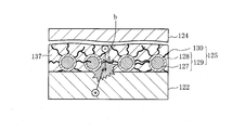
また、特許文献3では、発光層126は量子ドット125の集合体のみで形成され、かつ、この発光層126上に電子輸送層124が形成されることから、図14に示すように、電子輸送層124の形成工程で、膜密度が十分緻密でなく、量子ドット125間が開いている場合、発光層126が電子輸送性材料137で充填されてしまうことがある。そしてこの場合、通常、界面活性剤の配位子の大きさはナノ粒子129の粒径と変わらないことから、キャリアはナノ粒子129に注入されずに両性界面活性剤130を伝って量子ドット125と量子ドット125との間隙に流れ込むおそれがある。そして、その結果、キャリアはナノ粒子129に注入されずに正孔輸送層122や電子輸送層124に入り込むおそれがあり、更には、図14中、bに示すように、充填された電子輸送性材料137中で電子は正孔と結合して励起子発光するおそれがある。すなわち、特許文献3では、ナノ粒子129のコア部127内で励起子発光せずに、充填された電子輸送性材料137中で励起子発光するキャリアが発生し、このため発光効率の低下や発光色純度の低下を招くおそれがある。
本発明はこのような事情に鑑みなされたものであって、量子ドット内へのキャリアの注入効率が良好な発光デバイス、及び該発光デバイスの製造方法を提供することを目的とする。
本発明者は上記目的を達成するために鋭意研究を行なったところ、電子のみ、又は正孔のみを輸送する2種類の界面活性剤で超微粒子を表面被覆し、これにより量子ドットを形成し、さらに緻密で耐電圧性に優れた高分子化合物からなる絶縁性材料で量子ドット間を充填することにより、キャリアの超微粒子内への注入効率を向上させることができ、これにより発光特性を向上させることができるという知見を得た。
本発明はこのような知見に基づきなされたものであって、本発明に係る発光デバイスは、発光層が量子ドットの集合体で形成された発光デバイスにおいて、前記量子ドットは、超微粒子の表面が正孔輸送性を有する第1の界面活性剤と電子輸送性を有する第2の界面活性剤とで被覆され、かつ、前記発光層は、前記量子ドット間が高分子化合物からなる絶縁性材料で充填されていることを特徴としている。
これにより前記第1の界面活性剤は正孔のみを輸送し、第2の界面活性剤は電子のみを輸送することができ、かつキャリアは超微粒子の内部に高効率で注入され、超微粒子の外部を通過してしまうのを抑制することができる。
したがって、電圧印加により電極に注入されたキャリアは、超微粒子の外部で正孔と電子が再結合することもなく、効率良く超微粒子内に輸送することができ、これにより、膜のキャリア輸送性が高いために膜厚を薄くせねばならない制限もなく、キャリアの超微粒子への注入効率を向上させることが可能となる。
また、本発明の発光デバイスは、前記高分子化合物は、ポリイミド系樹脂、アクリル系樹脂、ポリスチレン系樹脂、ポリカーボネート系樹脂、ポリエステル系樹脂、ポリアミド系樹脂、及びポリビニル系樹脂の群から選択された1種以上を含むのが好ましい。
また、電子輸送性の第1の界面活性剤及び正孔輸送性の第2の界面活性剤と量子ドットとの間を、トンネル共鳴を利用してキャリア移動させることにより、フォノンボトルネックが生じることなく迅速かつ効率よくキャリアを輸送することができる。そのためには第1の界面活性剤は、前記量子ドットの価電子帯とトンネル共鳴するようなHOMO準位を有するのが好ましく、第2の界面活性剤は、前記量子ドットの伝導帯とトンネル共鳴するようなLUMO準位を有するのが好ましい。
すなわち、本発明の発光デバイスは、前記第1の界面活性剤は、前記超微粒子の価電子帯とトンネル共鳴するようなHOMO準位を有するのが好ましい。
さらに、本発明の発光デバイスは、前記HOMO準位は、前記価電子帯のエネルギー準位に対し-0.2~+0.2eVであるのが好ましい。
このように第1の界面活性剤は、超微粒子である量子ドットの価電子帯とトンネル共鳴するようなHOMO準位、例えば、前記価電子帯のエネルギー準位に対し、-0.2~+0.2eVとすることにより、正孔はトンネル共鳴により量子ドットと界面活性剤の間を迅速に移動する。
また、本発明の発光デバイスは、前記第2の界面活性剤は、前記超微粒子の伝導帯とトンネル共鳴するようなLUMO準位を有するのが好ましい。
さらに、本発明の発光デバイスは、前記LUMO準位は、前記伝導帯のエネルギー準位に対し-0.2~+0.2eVであるのが好ましい。
このように第2の界面活性剤は、前記超微粒子である量子ドットの伝導帯とトンネル共鳴するようなLUMO準位、例えば、前記伝導帯のエネルギー準位に対し、-0.2~+0.2eVとすることにより、電子はトンネル共鳴により量子ドットと界面活性剤の間を迅速に移動する。
このように界面活性剤が有する配位子のエネルギー準位を調整することによって、トンネル共鳴を利用したキャリア移動を行うことができ、フォノンボトルネックが生じることなく効率の良いキャリア輸送を実現することができる。すなわち、フォノンボトルネックを回避するために、煩雑な成膜プロセスを要する量子井戸層やトンネル層を形成する必要もなく、超微粒子への効率の良いキャリア注入が可能な発光デバイスを実現することが可能となる。
また、本発明の発光デバイスは、前記超微粒子は、酸化物、化合物半導体、及び単体半導体のいずれかを含むのが好ましい。
また、本発明の発光デバイスは、前記超微粒子は、コア部と該コア部を被覆するシェル部とからなるコアーシェル構造を有しているのが好ましい。
また、本発明の発光デバイスは、前記発光層の一方の主面に正孔輸送層が形成されると共に、前記発光層の他方の主面に電子輸送層が形成されているのが好ましい。
また、上記発光層は、量子ドット分散溶液と絶縁性溶液とを混合させた混合溶液を調製することにより、煩雑な複数の成膜プロセスを要することなく、安価かつ効率良く製造することができる。
すなわち、本発明に係る発光デバイスの製造方法は、正孔輸送性界面活性剤及び電子輸送性界面活性剤で超微粒子を被覆した量子ドット分散溶液を作製する量子ドット分散溶液作製工程と、高分子化合物からなる絶縁性材料を溶剤に溶解させて絶縁性溶液を作製する絶縁性溶液作製工程と、前記量子ドット分散溶液と前記絶縁性溶液とを混合して混合溶液を作製する混合溶液作製工程と、前記混合溶液を使用して発光層を作製する発光層作製工程とを含むことを特徴としている。
また、本発明の発光デバイスの製造方法は、透明基板の表面に第1の導電性材料を付与して第1の電極層を形成する第1の電極層形成工程と、前記第1の電極層の表面に正孔輸送性材料を付与し、正孔輸送層を形成する正孔輸送層形成工程と、前記発光層の表面に電子輸送性材料を付与し、電子輸送層を形成する電子輸送層形成工程と、前記電子輸送層の表面に第2の導電性材料を付与して第2の電極層を形成する第2の電極層形成工程とを含み、前記発光層形成工程は、前記正孔輸送層の表面に前記混合溶液を付与して前記発光層を形成するのが好ましい。
これにより隣接する正孔輸送層や電子輸送層が無機材料或いは有機材料のいずれで形成されていても、キャリアの隣接層へのリークが抑制され、超微粒子への注入効率が良好な高品質の発光デバイスを安価かつ高効率で製造することができる。
本発明の発光デバイスによれば、量子ドットは、超微粒子の表面が正孔輸送性を有する第1の界面活性剤と電子輸送性を有する第2の界面活性剤とで被覆され、かつ、前記発光層は、前記量子ドット間が高分子化合物(ポリイミド系樹脂、アクリル系樹脂、ポリスチレン系樹脂、ポリカーボネート系樹脂、ポリエステル系樹脂、ポリアミド系樹脂、及びポリビニル系樹脂等)からなる絶縁性材料で充填されているので、前記第1の界面活性剤は正孔のみを輸送し、第2の界面活性剤は電子のみを輸送することができ、かつキャリアは超微粒子の内部に高効率で注入され、超微粒子の外部を通過してしまうのを抑制することができる。
したがって、電圧印加により電極に注入されたキャリアは、超微粒子の外部で正孔と電子が再結合することもなく、効率良く超微粒子内に輸送することができ、これにより、膜のキャリア輸送性が高いために膜厚を薄くせねばならない制限もなく、キャリアの超微粒子への注入効率を向上させることが可能となる。
また、本発明の発光デバイスの製造方法によれば、正孔輸送性界面活性剤及び電子輸送性界面活性剤で超微粒子を被覆した量子ドット分散溶液を作製する量子ドット分散溶液作製工程と、高分子化合物からなる絶縁性材料を溶剤に溶解させて絶縁性溶液を作製する絶縁性溶液作製工程と、前記量子ドット分散溶液と前記絶縁性溶液とを混合して混合溶液を作製する混合溶液作製工程と、前記混合溶液を使用して発光層を作製する発光層作製工程とを含むので、ドライプロセスのような複数の煩雑な成膜プロセスを要することなく、1プロセスで発光層を作製することが可能であり、安価で効率良く製造することができる。
次に、本発明の実施の形態を詳説する。
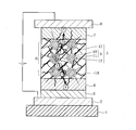
図1は、本発明に係る発光デバイスとしての発光ダイオードの一実施の形態を模式的に示す断面図である。
この発光ダイオードは、ガラス基板1(透明基板)上に陽極2が形成され、該陽極2の表面に正孔輸送性材料からなる正孔注入層3及び正孔輸送層4が順次形成され、該正孔輸送層4の表面に量子ドット層5の集合体からなる発光層6が形成され、さらに発光層6の表面には電子輸送性材料からなる電子輸送層7が形成され、該電子輸送層7の表面には陰極8が形成されている。
量子ドット5は、図2に示すように、ナノ粒子(超微粒子)9がコア部10と該コア部10を保護するシェル部11とを有するコアーシェル構造からなり、該シェル部11の表面が正孔輸送性を有する正孔輸送性界面活性剤(第1の界面面活性剤)12と電子輸送性を有する電子輸送性界面活性剤(第2の界面活性剤)13とで被覆されている。そして、正孔輸送層4から輸送されてきた正孔と電子輸送層7から輸送されてきた電子とが、ナノ粒子9のコア部10に注入されて正孔と電子とがコア部10内で再結合し、励起子発光する。
ここで、コア部10を形成するコア材料としては、光電変換作用を奏する半導体材料であれば特に限定されるものではなく、InP、CdSe、CdS、PbSe等を使用することができ、また、シェル部11を構成するシェル材料としては、例えばZnSを使用することができる。
上記正孔輸送性界面活性剤12としては、低分子の正孔輸送層用材料に配位子を導入した材料を使用することができる。
ここで、低分子の正孔輸送層用材料としては、例えば、化学式(1)で表わされるN,N′-ジフェニル-N,N′-ビス(3-メチルフェニル)-1,1′-ビフェニル-4,4′-ジアミン(以下、「TPD」という。)、化学式(2)で表わされる4,4′-ビス[N-(1-ナフチル)-N-フェニル-アミノ]ビフェニル(以下、「α-NPD」という。)、化学式(3)で表わされる4,4′,4″-トリス(2-ナフチルフェニルアミノ)トリフェニルアミン(以下、「2-TNATA」という。)、化学式(4)で表わされるN,N′-7-ジ(1-ナフチル)-N,N′-ジフェニル-4,4′-ジアミノビフェニル(以下、「Spiro-NPB」という。)、化学式(5)で表わされる4,4′,4″-トリス(3-メチルフェニルフェニルアミノ)トリフェニルアミン(以下、「m-MTDATA」という。)、及びこれらの誘導体を使用することができる。


また、配位子としては、極性基であれば特に限定されるものではなく、例えば、チオール基(-SH)、アミノ基(-NH2)、カルボキシル基(-COOH)、カルボニル基(-CO)、ニトロ基(-NO2)、ホスフィノ基(-PH2)、ホスホロソ基(-PO)等を1つ又は2つ以上使用することができる。
したがって、正孔輸送性界面活性剤12としては、例えば、TPDにチオール基を導入したTPD-チオール配位子、α-NPDにアミノ基を導入したα-NPD-アミノ配位子等を使用することができる。そして、配位子の導入個数が1つの場合は、非極性溶媒に分散させることができ、配位子の導入個数が2つ以上の場合は極性溶媒にも分散させることができる。
尚、ポリ(3,4-エチレンジオキシチオフェン):ポリ(スチレンスルフォネート)(以下、「PEDOT:PSS」という。)のような高分子材料は、正孔輸送層用材料としては好適に使用することができるが、正孔輸送性界面活性剤用材料に使用するのは好ましくない。高分子材料は、分子サイズが大きく、これが立体障害となるため、隣接距離を短くすることができず、その結果、ナノ粒子9の表面被覆率が低下して量子収率の低下を招いたり、量子ドット5の面密度を上げることができない。
また、電子輸送性界面活性剤13としては、電子輸送層用材料に配位子を導入した材料を使用することができる。
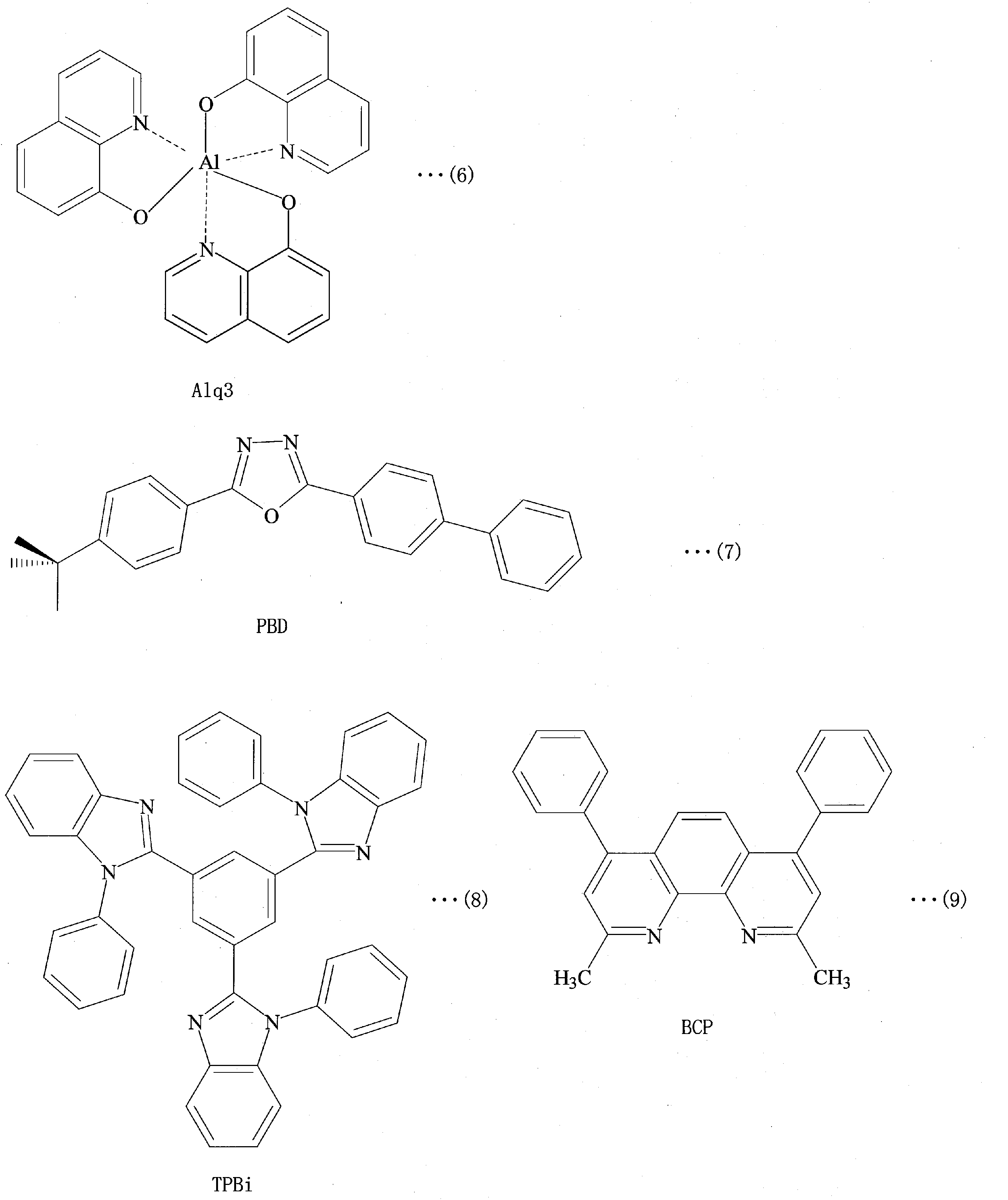
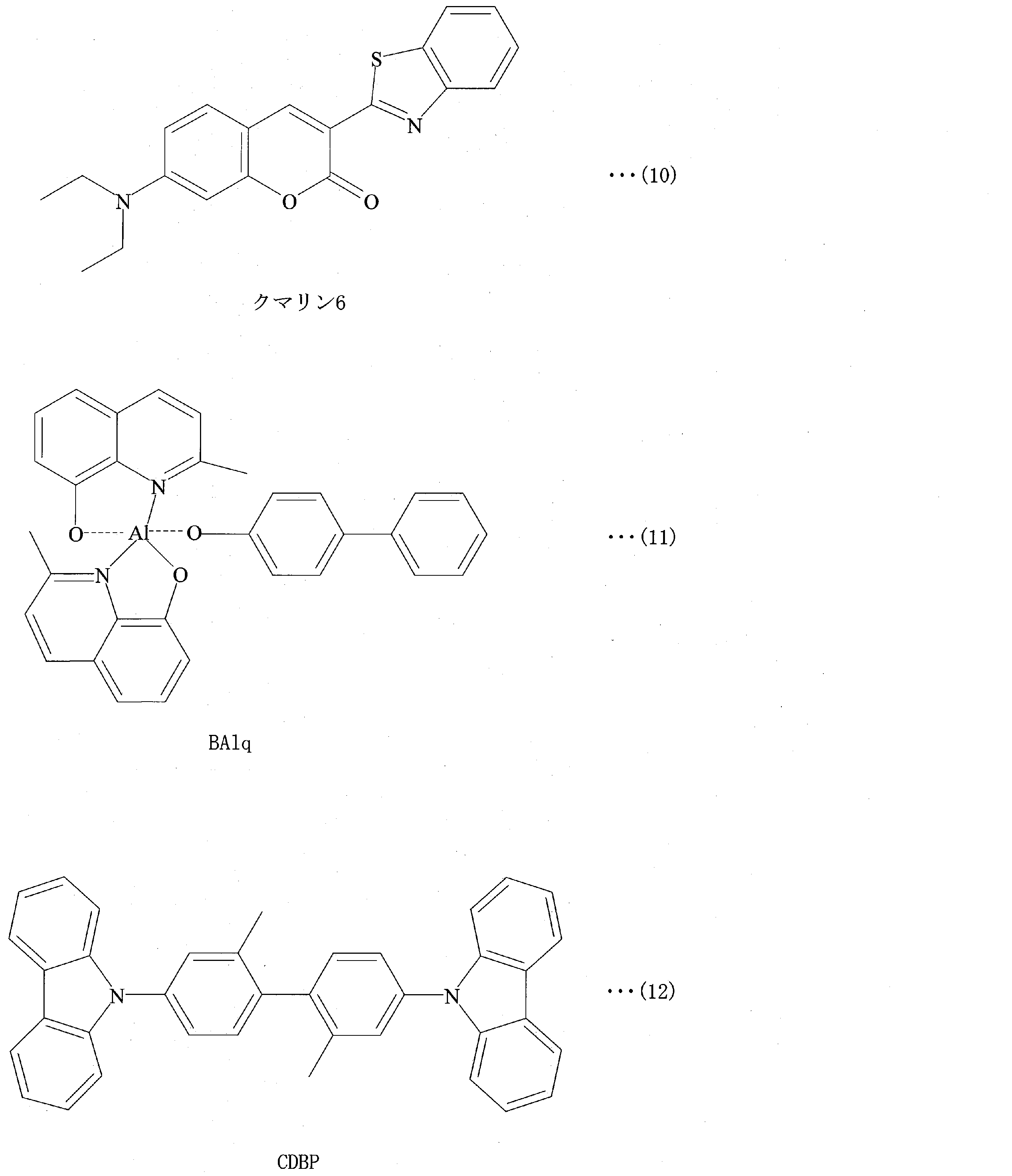
ここで、電子輸送層用材料としては、例えば、化学式(6)で表わされるトリス(8-ヒドロキシキノリン)アルミニウム(以下、「Alq3」という。)、化学式(7)で表わされる2-(4-ビフェニリル)-5-(4-t-ブチルフェニル)-1,3,4-オキサジアゾール(以下、「PBD」という。)、化学式(8)で表わされる2,2′,2″-(1,3,5-ベンジニトリル)-トリス(1-フェニル-1-H-ベンゾイミダゾール(以下、「TPBi」という。)、化学式(9)で表わされる2,9-ジメチル-4,7-ジフェニル-1,10-フェナントロリン(以下、「BCP」という。)、化学式(10)で表わされる3-(ベンゾチアゾール-2-イル)-7-(ジエチルアミノ)-2H-1-ベンゾピラン-2-オン(以下、「クマリン6」という。)、化学式(11)で表わされるビス(2-メチル-8-キノリノラート)-4-(フェニルフェノラート)アルミニウム(以下、「BAlq」という。)、化学式(12)で表わされる4,4′-ビス(9-カルバゾリル)-2,2′-ジメチルビフェニル(以下、「CDBP」という。)、及びこれらの誘導体を使用することができる。
また、配位子としては、正孔輸送性界面活性剤12と同様、極性基であれば特に限定されるものではなく、例えば、チオール基(-SH)、アミノ基(-NH2)、カルボキシル基(-COOH)、カルボニル基(-CO)、ニトロ基(-NO2)、ホスフィノ基(-PH2)、ホスホロソ基(-PO)等を使用することができる。
したがって、電子輸送性界面活性剤13としては、例えば、PBDにチオール基を導入したPBD-チオール配位子、BCPにアミノ基を導入したBCP-アミノ配位子等を使用することができる。
このように正孔輸送性界面活性剤12と電子輸送性界面活性剤13とが併存した状態でナノ粒子9の表面を被覆することにより、正孔のみ、及び電子のみがそれぞれの界面活性剤(正孔輸送性界面活性剤12及び電子輸送性界面活性剤13)を介して輸送される。そしてその結果、界面活性剤中での電子-正孔の再結合が抑制され、効率の良いキャリア(電子及び正孔)の輸送が可能となる。
また、発光層6は、量子ドット5の間隙に絶縁性材料14が充填されている。
量子ドット5内、すなわち量子ドット5のコア部10内でキャリアを再結合させて効率よく励起子発光させるためには、量子ドット5の近傍に輸送されてきたキャリアをコア部10内に効率的に注入する必要がある。
しかしながら、ナノ粒子9の表面は正孔輸送性界面活性剤12及び電子輸送性界面活性剤13の配位子によって被覆されているため、量子ドット5の面密度を向上させてもナノ粒子9間には一定の間隙が生じる。したがって、キャリアは、ナノ粒子9のコア部10内に効率良くキャリアの注入されずに、コア部10の外部で再結合したり、或いは互いに対向する正孔輸送層3又は電子輸送層7に流れてしまい、その結果、発光色純度や発光効率の低下を招くおそれがある。
そこで、本実施の形態では、量子ドット5間の間隙を緻密で耐電圧性に優れた絶縁性材料14で充填している。
このような絶縁性材料としては、高分子化合物が好ましい。無機材料の場合は結晶粒界が形成されるため、キャリアはナノ粒子9のコア部10に注入されずに、前記結晶粒界を伝わるような形態で該ナノ粒子9の周辺を通過したり、或いは結晶粒界で電子と正孔が再結合するおそれがあり、好ましくない。
そして、このような高分子化合物としては、特に限定されるものではなく、例えば、ポリイミド系樹脂、ポリメタクリル酸メチル(PMMA)やポリアクリレート等のアクリル系樹脂、単独重合スチレンやアクリルニトリル-スチレンモノマー共重合体(AS)或いはアクリルニトリル-ブタジエン-スチレン共重合体(ABS)等のポリスチレン系樹脂、ポリカーボネート系樹脂、ナイロン等のポリアミド系樹脂、ポリエステル系樹脂、ポリ酢酸ビニルやポリ塩化ビニル等のポリビニル系樹脂等を使用することができる。
このように形成された発光ダイオードでは、電圧が印加されると、陽極2及び陰極8にキャリアが注入される。そして、注入されたキャリアのうち、陽極2に注入された正孔は、正孔輸送性界面活性剤12のバルクへテロ的なネットワーク内を伝ってナノ粒子9内に注入される。一方、陰極8に注入された電子は、電子輸送性界面活性剤13のバルクへテロ的なネットワークの内部を伝ってナノ粒子9内に注入され、コア部10内で正孔と電子とが再結合し、発光する。
このように本実施の形態では、正孔及び電子は、量子ドット5の間隙に流れ込むこともなく、正孔輸送性界面活性剤12及び電子輸送性界面活性剤13を介してそれぞれ別経路でナノ粒子9の内部に輸送されるので、正孔と電子とは輸送中に近づいて再結合することがなく、10μmレベルの比較的厚い膜厚でも効率良く輸送することができる。そしてこれにより電気信号から光信号への光電変換を高効率で行なうことができる。
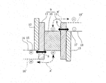
図3は、各界面活性剤12、13のエネルギー準位とナノ粒子9の量子化されたキャリアのエネルギー準位の関係を示す図である。
正孔輸送性界面活性剤12は、正孔が移動できるエネルギー帯であるコア部10の価電子帯のエネルギー準位(以下、「価電子帯準位」という。)15とトンネル共鳴するようなHOMO準位16を有し、電子輸送性界面活性剤13は、電子が移動できるエネルギー帯であるナノ粒子9のコア部10の伝導帯のエネルギー準位(以下、「伝導帯準位」という。)17とトンネル共鳴するようなLUMO準位18を有している。
そして、このようにトンネル共鳴を利用することにより、キャリアは容易にエネルギー障壁を通り抜けることができ、効率の良いキャリア移動を実現することが可能となる。
図4は、トンネル共鳴によるキャリア移動の原理を示す模式図である。
ナノ粒子9は、上述したようにコア部10とシェル部11とからなる。そして、シェル部11は通常1nm以下の超薄膜であるため、トンネル効果によりキャリアは容易に通過するが、コア部10と界面活性剤12、13との間のキャリア移動も迅速に行なってキャリアの輸送効率を向上させるのが望ましい。
しかしながら、正孔輸送性界面活性剤12のHOMO準位16′とコア部10の価電子帯準位15とがトンネル共鳴しないような大きなエネルギー準位差を有する場合は、矢印A′に示すようにエネルギー障壁を乗り越えるようにして正孔は移動する。同様に、電子輸送性界面活性剤13のLUMO準位18′とコア部10の伝導帯準位17とがトンネル共鳴しないような大きなエネルギー準位差を有する場合は、矢印B′に示すようにエネルギー障壁を乗り越えるようにして電子は移動する。
しかも、ナノ粒子系ではフォノンの移動が遅く、フォノンの遅い移動に律速されてフォノンボトルネックが生じるため、キャリアの迅速な移動が困難となる。
そこで、本実施の形態では、正孔輸送性界面活性剤12が、コア部10の価電子帯準位15とトンネル共鳴するようなHOMO準位16を有し、また、電子輸送性界面活性剤13が、コア部10の伝導帯準位17とトンネル共鳴するようなLUMO準位18を有するようにし、これにより矢印A、Bに示すようにキャリアの移動を迅速に行ない、キャリアの輸送効率向上を図っている。
尚、このようなトンネル共鳴を生じさせるためには、正孔輸送性界面活性剤12のHOMO準位16は、コア部10の価電子帯準位15に対し-0.2~+0.2eVの範囲が好ましく、例えば、コア部10にInP(価電子帯準位:5.7eV)を使用する場合は、TPD-チオール配位子(HOMO準位:5.6eV)を使用することができる。
また、電子輸送性界面活性剤13のLUMO準位18は、コア部10の伝導帯準位17に対し-0.2~+0.2eVの範囲が好ましく、例えば、コア部10にInP(伝導帯準位:約3eV)を使用する場合は、BCP-アミノ配位子(LUMO準位:3.2eV)を使用することができる。
次に、上記発光ダイオードの製造方法を説明する。
ナノ粒子9は、上述したように種々の材料を使用して作製することができるが、下記の実施の形態では、コア部10にInP、シェル部11にZnSを使用した場合を例に説明する。
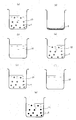
図5は量子ドット分散溶液の作製手順を示す製造工程図である。
まず、図5(a)に示すように、InP/ZnSをナノ粒子9とする原料溶液19を作製する。
すなわち、例えば、酢酸インジウム、ミリスチン酸及びオクタデセンを容器中で混合し、窒素雰囲気中、撹拌して溶解させ、これによりインジウム前駆体溶液を調製する。さらに、窒素雰囲気中、トリストリメチルシリルホスフィン、オクチルアミン、オクタデセンを混合し、これによりリン前駆体溶液を調製する。
次いで、インジウム前駆体溶液を所定温度(例えば、190℃)に加熱し、この加熱溶液中にリン前駆体溶液を注入する。すると、高温により活性度の高い前駆体同士が反応し、インジウムとリンが結合して核を形成し、その後周囲の未反応成分と反応して結晶成長が起り、これによりInP量子ドットが作製される。
次に、酸化亜鉛をステアリン酸に溶解させた酸化亜鉛溶液、及びイオウをステアリン酸に溶解させたイオウ溶液を用意する。
次いで、所定温度(例えば、150℃)に調整されたInP量子ドット溶液に酸化亜鉛溶液及びイオウ溶液を交互に微量ずつ滴下し、加熱・冷却し、洗浄して溶液中の過剰有機成分を除去する。そしてこの後、ヘキサデシルアミン(以下、「HDA」という。)等の有機化合物からなる界面活性剤を添加しつつ、分散溶媒、例えばヘキサン中に分散させ、これにより界面活性剤で被覆されたInP/ZnSをナノ粒子9とするInP/ZnS分散溶液、すなわち原料溶液19が作製される。
次いで、正孔輸送性界面活性剤12及び電子輸送性界面活性剤13を等量ずつ秤量し、有機溶媒、例えばヘキサンに溶解させ、図5(b)に示すように、界面活性剤溶液20を作製する。
次いで、原料溶液19と界面活性剤溶液20とを、界面活性剤溶液20が原料溶液19に対して2倍程度の混合比率となるように混合し、配位子置換を行う。
すなわち、界面活性剤溶液20が原料溶液19よりも2倍程度多い状態で原料溶液19と界面活性剤溶液20とを混合し、十分に長い時間放置すると、正孔輸送性界面活性剤12及び電子輸送性界面活性剤13とが等量ずつ存在することから、原料溶液19中の界面活性剤が界面活性剤溶液20中の正孔輸送性界面活性剤12及び電子輸送性界面活性剤13と置換され、これにより、図5(c)に示すように、正孔輸送性界面活性剤12と電子輸送性界面活性剤13とが併存した量子ドット5を有する配位子置換溶液21が得られる。
尚、ナノ粒子9同士の凝集を避けるために、HDA等の有機化合物からなる界面活性剤でナノ粒子9を被覆しているが、界面活性剤として通常の有機化合物を使用して発光層を形成しても、有機分子に起因した界面活性剤の低導電性のために電位障壁が大きく、このためキャリア(正孔及び電子)を介した発光効率が低下するおそれがある。
また、界面活性剤として導電性高分子や金属系材料を使用した場合は、電圧印加により電極に注入されたキャリアは、陽極から陰極へ、又は陰極から陽極へと界面活性剤中を通過してしまい、キャリアを量子ドット内に効率良く閉じ込めるのは困難である。
これに対し本実施の形態では、配位子置換を行ってナノ粒子9を正孔輸送性の配位子を有する正孔輸送性界面活性剤12、及び電子輸送性の配位子を有する電子輸送性界面活性剤12で被覆し、これにより電子のみ、又は正孔のみを効率良く輸送できるようにし、キャリアのナノ粒子9への注入効率向上を図っている。
次に、配位子置換溶液21に大量のメタノール等の有機溶剤を投入し、遠心分離機等で分離し、上澄み液を除去した後、図5(d)に示すように、真空乾燥させて溶剤成分を完全に除去する。
次いで、量子ドット5を、絶縁性材料14が溶解可能な分散溶媒に溶解させ、これにより図5(e)に示すように、量子ドット分散溶液22を作製する。
一方、図5(f)に示すように、絶縁性材料14を前記分散溶媒と同種の有機溶媒に溶解させて絶縁性溶液23を作製する。
そして、量子ドット分散溶液22と絶縁性溶液23とを混合させ、図5(g)に示すように、混合溶液24を作製する。
尚、絶縁性材料14を溶解させる有機溶媒は、使用する絶縁性材料14に応じて適宜選択することができる。
すなわち、有機溶媒としては、例えば、絶縁性材料14にポリイミド系樹脂を使用する場合は、N-メチル-2-ピロリドンやγ-ブチロラクトン等の五員環ラクタム構造を有する化合物を使用することができる。また、絶縁性材料14にアクリル系樹脂やポリカーボネート樹脂、ポリエステル系樹脂を使用する場合は、ベンゼン、トルエン、キシレン等の芳香族炭化水素、トリクレン、クロロベンゼン、ジクロロエタン、クロロホルム等の塩素含有炭化水素、エステル系有機化合物、ケトン系有機化合物等を使用することができる。絶縁性材料14にポリスチレン系樹脂を使用する場合は、上述した芳香族炭化水素、塩素含有炭化水素の他、アセトン、メタノール、エタノール等を使用することができる。また、絶縁性材料14にポリアミド系樹脂を使用する場合は、フェノールやメタノールを使用することができる。さらにポリ酢酸ビニル樹脂を絶縁性材料14に使用する場合は、上述した芳香族炭化水素、塩素含有炭化水素の他、アニリン、ピリジンを使用することができ、ポリ塩化ビニル樹脂を使用する場合は、上述した塩素含有炭化水素やアセトンを使用することができる。
そして、このような高分子化合物に溶解する有機溶媒に応じて量子ドット分散溶液22の分散溶媒が選択される。例えば、絶縁性材料14にPMMAを使用する場合は、PMMAが溶解するトルエンを絶縁性溶液23の有機溶媒及び量子ドット分散溶液22の分散溶媒に選択することができる。そして、この選択された分散溶媒に分散可能な正孔輸送性界面活性剤12及び電子輸送性界面活性剤13が使用される。
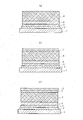
図6及び図7は上記発光ダイオードの製造方法を示す製造工程図である。
図6(a)に示すように、スパッタ法によりガラス基板1上にITO膜を成膜し、UVオゾン処理を行い、膜厚100nm~150nmの陽極2を形成する。
次に、正孔注入層用界面活性剤溶液(以下、「正孔注入層用溶液」という。)を用意する。ここで、正孔注入層用材料としては、正孔輸送層用材料と同様の材料を使用することができ、例えば、PEDOT:PSS等を使用することができる。
そして、スピンコート法等を使用して正孔注入層用溶液を陽極2上に塗布し、図6(b)に示すように、膜厚20nm~30nmの正孔注入層3を形成する。
次に、正孔注入層用材料よりもHOMO準位の低いエネルギーを有する正孔輸送層用界面活性剤溶液(以下、「正孔輸送層用溶液」という。)を用意する。ここで、例えば、PEDOT:PSSを正孔注入層用材料に使用した場合は、正孔輸送層用材料として、該PEDOT:PSSよりもHOMO準位の低いポリ-TPD等を使用することができる。
そして、スピンコート法等を使用して正孔輸送層用溶液を正極注入層3上に塗布し、図6(c)に示すように、膜厚60nm~70nmの正孔輸送層4を形成する。
尚、上記正孔注入層3は、正孔の輸送性を向上させるために設けたものであることから、正孔輸送層4が正孔注入層3を兼用してもよく、この場合は正孔輸送層4をポリ-TPDのみで形成し、正孔注入層3を省略することができる。
次に、上述した混合溶液24を用意する。
そして、スピンコート法等を使用し、混合溶液24を正孔輸送層4上に塗布し、図7(d)に示すように、積層構造を有する膜厚300nm~1000nmの発光層6を形成する。
次に、Alq3等の電子輸送性材料を使用し、図7(e)に示すように、真空蒸着法で発光層6の表面に膜厚50nm~70nmの電子輸送層7を形成する。
そして、図7(f)に示すように、LiF、Al等を使用し、真空蒸着法で膜厚100nm~300nmの陰極8を形成し、これにより発光ダイオードが作製される。
このように本実施の形態では、正孔輸送性界面活性剤12及び電子輸送性界面活性剤13でナノ粒子9を被覆した量子ドット分散溶液22を作製する一方、高分子化合物からなる絶縁性材料14を溶媒に溶解させて絶縁性溶液23を作製し、量子ドット分散溶液22と絶縁性溶液23とを混合して混合溶液24を作製し、この混合溶液24を正孔輸送層4の表面に塗付して発光層6を形成しているので、ドライプロセスのような複数の煩雑な成膜プロセスを要することなく、1プロセスで発光層を作製することが可能となり、安価で効率良く製造することができる。
また、発光層6に隣接する正孔輸送層4及び電子輸送層7が無機材料或いは有機材料のいずれで形成されていても、キャリアの隣接層へのリークを抑制することができ、ナノ粒子9への注入効率が良好な高品質の発光デバイスを安価かつ高効率で製造することができる。
そしてこのようにして形成された発光ダイオードは、正孔輸送性界面活性剤12で正孔のみを輸送し、電子輸送性界面活性剤13で電子のみを輸送することができ、しかも量子ドット5間は絶縁性材料14で充填されているので、キャリアがナノ粒子9の内部に高効率で注入され、ナノ粒子9の外部を通過してしまうのを抑制することができる。
すなわち、電圧印加により電極に注入されたキャリアは、ナノ粒子9の外部で正孔と電子が再結合することもなく、効率良く量子ドット内に輸送することができる。そしてこれにより、キャリアの超微粒子への注入効率を向上させることが可能となる。
また、界面活性剤が有する配位子のエネルギー準位を調整することによって、トンネル共鳴を利用したキャリア移動を行うことができ、フォノンボトルネックが生じることなく効率の良いキャリア輸送を実現することができる。すなわち、フォノンボトルネックを回避するために、煩雑な成膜プロセスを要する量子井戸層やトンネル層を形成する必要もなく、ナノ粒子9への効率の良いキャリア注入が可能な発光デバイスを実現することが可能となる。
尚、本発明は上記実施の形態に限定されるものでない。上記実施の形態では、ナノ粒子9は、コア部10を1層のシェル部11で被覆したコアーシェル構造を有しているが、シェル部が2層構造のコアーシェルーシェル構造や、シェル部のない場合にも同様に適用できる。
また、上記実施の形態では、ナノ粒子9としてInP/ZnSからなる化合物半導体を使用したが、酸化物や単体半導体であってもよいのはいうまでもない。
また、上記実施の形態では、発光デバイスとして発光ダイオードの場合について説明したが、半導体レーザや各種表示装置等の各種発光デバイスに使用できるのはいうまでもない。
また、上記実施の形態では、電子輸送層7は真空蒸着法を使用したドライプロセスで行っているが、スピンコート法等のウェットプロセスで作製してもよい。ただし、この場合は、浸漬工程で使用した分散溶液と同じ極性の分散溶媒を使用する必要がある。
〔試料の作製〕
(試料番号1)
コア部がInP、シェル部がZnSで形成されたInP/ZnSナノ粒子を界面活性剤としてのHDAで被覆し、ヘキサン溶液に分散させた濃度が5mg/mLの原料溶液を用意した。
(試料番号1)
コア部がInP、シェル部がZnSで形成されたInP/ZnSナノ粒子を界面活性剤としてのHDAで被覆し、ヘキサン溶液に分散させた濃度が5mg/mLの原料溶液を用意した。
次いで、正孔輸送性界面活性剤としてTPD-チオール配位子、及び電子輸送性界面活性剤としてBCP-アミノ配位子をそれぞれ用意し、界面活性剤の濃度が0.1mol/Lとなるようにこれらを等量ずつ秤量し、ヘキサンに溶解させて界面活性剤溶液を作製した。
次いで、原料溶液と界面活性剤溶液とを、原料溶液:界面活性剤溶液=1:2となるように両者を混合し、24時間放置し、HDAをTPD-チオール配位子及びBCP-アミノ配位子で置換し、量子ドットを含有した配位子置換溶液を得た。
次に、配位子置換溶液に対し5倍のメタノールを投入し、遠心分離機で分離し、上澄み液を除去し、その後真空乾燥させてメタノールを完全に除去した。
次いで、量子ドットの濃度が2~5mg/mLとなるように量子ドットをトルエン中に分散させ、量子ドット分散溶液を作製した。
次いで、絶縁性材料としてのPMMAをトルエンに溶解させ、濃度が0.1Mol/mLの絶縁性溶液を作製した。
その後、量子ドット分散溶液と絶縁性溶液とを混合させ、量子ドットの濃度が0.8mg/mLの混合溶液を作製した。
次に、スパッタ法によりガラス基板上にITO膜を成膜し、UVオゾン処理を行い、膜厚120nmの陽極を作製した。
次に、正孔注入層用材料としてのPEDOT:PSSを純水に分散させて正孔注入層用溶液を作製した。
そして、スピンコート法を使用して正孔注入層用溶液を陽極上に塗布し、膜厚20nmの正孔注入層を形成した。
次に、正孔輸送層用材料としてのポリ-TPDをクロロベンゼンに分散させて正孔輸送層用溶液を作製した。
そして、スピンコート法を使用して正孔輸送層用溶液を正孔注入層上に塗布し、膜厚65nmの正孔輸送層を作製した。
次に、スピンコート法を使用し、上述した混合溶液を正孔輸送層上に塗布し、発光層を形成した。具体的には、発光層の厚みが1モノレイヤー(単分子層)となるように、スピンコート法で発光層を形成した。すなわち、混合溶液:0.1mLを正孔輸送層に滴下し、ガラス基板を回転数:3000rpmで60秒間回転させて発光層を作製した。尚、本実施例で発光層の厚みを1モノレイヤーとしたが、これはナノ粒子が1粒子分の厚みでかつ僅かに隙間が生じている状態を意味する。
次に、電子輸送性材料としてAlq3を使用し、真空蒸着法で発光層の表面に膜厚50nmの電子輸送層を作製した。尚、発光層の厚みは1モノレイヤーであるが、この電子輸送層は発光層上に形成されることから、電子輸送層を形成するAlq3は、量子ドットの僅かな間隙に流れ込んでいると推測される。
そして、LiF及びAlを使用し、真空蒸着法で二層構造からなる膜厚が250nmの陰極を形成し、これにより試料番号1の試料を作製した。
(試料番号2)
上述した混合溶液を使用する代わりに、量子ドット分散溶液を使用し、該量子ドット分散溶液を正孔輸送層上に厚みが1モノレイヤーとなるように塗布し、発光層を形成した。それ以外は、試料番号1と同様の方法・手順で、試料番号2の試料を作製した。
上述した混合溶液を使用する代わりに、量子ドット分散溶液を使用し、該量子ドット分散溶液を正孔輸送層上に厚みが1モノレイヤーとなるように塗布し、発光層を形成した。それ以外は、試料番号1と同様の方法・手順で、試料番号2の試料を作製した。
〔試料の評価〕
試料番号1、2について、直流電圧を印加し、プリズムとCCDで構成されたマルチチャネルアナライザを使用して発光スペクトルを測定した。
試料番号1、2について、直流電圧を印加し、プリズムとCCDで構成されたマルチチャネルアナライザを使用して発光スペクトルを測定した。
図8はその測定結果を示している。横軸が波長(nm)、縦軸が発光スペクトル(a.u.)であり、上側が試料番号1、下側が試料番号2の測定結果を示している。
試料番号2は、波長が614nm付近で発光スペクトルがピークに達しているが、535nm付近の波長域でも発光スペクトルが出現し、発光色の純度が低下した。これは電子輸送性材料であるAlq3が量子ドット間に流れ込み、ナノ粒子内で再結合するキャリアが存在する一方で、一部の正孔は隙間に充填された電子輸送性材料中、もしくは量子ドット層に隣接する電子輸送層中で電子と再結合し、Alq3の吸収波長域である535nm付近でも発光したものと思われる。
これに対し試料番号1は、緻密で耐電圧性に優れたPMMAで量子ドット間が充填されているので、量子ドット発光の614nm付近の波長域のみで発光し、隣接電子輸送層の発光のない良好な発光色純度が得られることが確認された。
キャリアのナノ粒子内部への注入効率を向上させて良好な発光効率を有する発光ダイオード等の発光デバイスを実現できる。
1 透明基板
2 陽極(第1の電極層)
4 正孔輸送層
5 量子ドット
6 発光層
7 電子輸送層
8 陰極(第2の電極層)
9 ナノ粒子(超微粒子)
10 コア部
11 シェル部
12 正孔輸送性界面活性剤(第1の界面活性剤)
13 電子輸送性界面活性剤(第2の界面活性剤)
14 絶縁性材料
15 価電子帯準位
16 HOMO準位
17 伝導帯準位
18 LUMO準位
22 量子ドット分散溶液
23 絶縁性溶液
24 混合溶液
2 陽極(第1の電極層)
4 正孔輸送層
5 量子ドット
6 発光層
7 電子輸送層
8 陰極(第2の電極層)
9 ナノ粒子(超微粒子)
10 コア部
11 シェル部
12 正孔輸送性界面活性剤(第1の界面活性剤)
13 電子輸送性界面活性剤(第2の界面活性剤)
14 絶縁性材料
15 価電子帯準位
16 HOMO準位
17 伝導帯準位
18 LUMO準位
22 量子ドット分散溶液
23 絶縁性溶液
24 混合溶液
Claims (11)
- 発光層が量子ドットの集合体で形成された発光デバイスにおいて、
前記量子ドットは、超微粒子の表面が正孔輸送性を有する第1の界面活性剤と電子輸送性を有する第2の界面活性剤とで被覆され、
かつ、前記発光層は、前記量子ドット間が高分子化合物からなる絶縁性材料で充填されていることを特徴とする発光デバイス。 - 前記高分子化合物は、ポリイミド系樹脂、アクリル系樹脂、ポリスチレン系樹脂、ポリカーボネート系樹脂、ポリエステル系樹脂、ポリアミド系樹脂、及びポリビニル系樹脂の群から選択された1種以上を含むことを特徴とする請求項1記載の発光デバイス。
- 前記第1の界面活性剤は、前記超微粒子の価電子帯とトンネル共鳴するようなHOMO準位を有することを特徴とする請求項1又は請求項2記載の発光デバイス。
- 前記HOMO準位は、前記価電子帯のエネルギー準位に対し-0.2~+0.2eVであることを特徴とする請求項3記載の発光デバイス。
- 前記第2の界面活性剤は、前記超微粒子の伝導帯とトンネル共鳴するようなLUMO準位を有することを特徴とする請求項1乃至請求項4のいずれかに記載の発光デバイス。
- 前記LUMO準位は、前記伝導帯のエネルギー準位に対し-0.2~+0.2eVであることを特徴とする請求項5記載の発光デバイス。
- 前記超微粒子は、酸化物、化合物半導体、及び単体半導体のいずれかを含むことを特徴とする請求項1乃至請求項6のいずれかに記載の発光デバイス。
- 前記超微粒子は、コア部と該コア部を被覆するシェル部とからなるコアーシェル構造を有していることを特徴とする請求項1乃至請求項7記載の発光デバイス。
- 前記発光層の一方の主面に正孔輸送層が形成されると共に、前記発光層の他方の主面に電子輸送層が形成されていることを特徴とする請求項1乃至請求項8のいずれかに記載の発光デバイス。
- 正孔輸送性界面活性剤及び電子輸送性界面活性剤で超微粒子を被覆した量子ドット分散溶液を作製する量子ドット分散溶液作製工程と、
高分子化合物からなる絶縁性材料を溶媒に溶解させて絶縁性溶液を作製する絶縁性溶液作製工程と、
前記量子ドット分散溶液と前記絶縁性溶液とを混合して混合溶液を作製する混合溶液作製工程と、
前記混合溶液を使用して発光層を作製する発光層作製工程とを含むことを特徴とする発光デバイスの製造方法。 - 透明基板の表面に第1の導電性材料を付与して第1の電極層を形成する第1の電極層形成工程と、
前記第1の電極層の表面に正孔輸送性材料を付与し、正孔輸送層を形成する正孔輸送層形成工程と、
前記発光層の表面に電子輸送性材料を付与し、電子輸送層を形成する電子輸送層形成工程と、
前記電子輸送層の表面に第2の導電性材料を付与して第2の電極層を形成する第2の電極層形成工程とを含み、
前記発光層形成工程は、前記正孔輸送層の表面に前記混合溶液を付与して前記発光層を形成することを特徴とする請求項10記載の発光デバイスの製造方法。
Priority Applications (1)
| Application Number | Priority Date | Filing Date | Title |
|---|---|---|---|
| JP2013505928A JP5828340B2 (ja) | 2011-03-24 | 2012-03-15 | 発光デバイス、及び該発光デバイスの製造方法 |
Applications Claiming Priority (2)
| Application Number | Priority Date | Filing Date | Title |
|---|---|---|---|
| JP2011066391 | 2011-03-24 | ||
| JP2011-066391 | 2011-03-24 |
Publications (1)
| Publication Number | Publication Date |
|---|---|
| WO2012128173A1 true WO2012128173A1 (ja) | 2012-09-27 |
Family
ID=46879323
Family Applications (1)
| Application Number | Title | Priority Date | Filing Date |
|---|---|---|---|
| PCT/JP2012/056681 Ceased WO2012128173A1 (ja) | 2011-03-24 | 2012-03-15 | 発光デバイス、及び該発光デバイスの製造方法 |
Country Status (2)
| Country | Link |
|---|---|
| JP (1) | JP5828340B2 (ja) |
| WO (1) | WO2012128173A1 (ja) |
Cited By (21)
| Publication number | Priority date | Publication date | Assignee | Title |
|---|---|---|---|---|
| WO2014097878A1 (ja) * | 2012-12-20 | 2014-06-26 | 株式会社村田製作所 | 発光デバイス、及び該発光デバイスの製造方法 |
| WO2014208456A1 (ja) * | 2013-06-25 | 2014-12-31 | コニカミノルタ株式会社 | 光学材料、光学フィルム及び発光デバイス |
| WO2015056750A1 (ja) * | 2013-10-17 | 2015-04-23 | 株式会社村田製作所 | ナノ粒子材料、及び発光デバイス |
| WO2015056749A1 (ja) * | 2013-10-17 | 2015-04-23 | 株式会社村田製作所 | ナノ粒子材料、及び発光デバイス |
| WO2015105027A1 (ja) * | 2014-01-09 | 2015-07-16 | 株式会社村田製作所 | 発光デバイス、及び発光デバイスの製造方法 |
| JP2016173888A (ja) * | 2015-03-16 | 2016-09-29 | 日本放送協会 | 発光素子及びその製造方法、並びに表示装置 |
| CN106328822A (zh) * | 2016-11-01 | 2017-01-11 | Tcl集团股份有限公司 | Qled及其制备方法 |
| CN106784345A (zh) * | 2016-12-08 | 2017-05-31 | 瑞声科技(南京)有限公司 | 量子点结构及制造方法、量子点发光二极管及制造方法 |
| CN107359264A (zh) * | 2017-08-03 | 2017-11-17 | 青岛海信电器股份有限公司 | 一种qled、制备方法及显示装置 |
| CN107394020A (zh) * | 2017-07-31 | 2017-11-24 | 京东方科技集团股份有限公司 | 一种发光器件的制作方法及发光器件、显示装置 |
| CN108352453A (zh) * | 2015-11-04 | 2018-07-31 | 广州华睿光电材料有限公司 | 电致发光器件、其制备方法及油墨组合物 |
| CN108447998A (zh) * | 2018-03-19 | 2018-08-24 | 京东方科技集团股份有限公司 | 量子点发光器件及制备方法、量子点发光显示装置 |
| CN109817815A (zh) * | 2017-11-20 | 2019-05-28 | 三星电子株式会社 | 量子点器件和显示设备 |
| WO2019180881A1 (ja) * | 2018-03-22 | 2019-09-26 | シャープ株式会社 | 表示デバイスおよびその製造方法 |
| JP2020132844A (ja) * | 2019-02-12 | 2020-08-31 | 東洋インキScホールディングス株式会社 | 量子ドット、量子ドット含有組成物、インクジェットインキ及び印刷物 |
| JP2020161369A (ja) * | 2019-03-27 | 2020-10-01 | 東洋インキScホールディングス株式会社 | 半導体微粒子組成物、及び電界発光素子 |
| WO2022074751A1 (ja) * | 2020-10-07 | 2022-04-14 | シャープ株式会社 | 発光素子の製造方法および発光素子 |
| CN114426839A (zh) * | 2020-10-28 | 2022-05-03 | Tcl科技集团股份有限公司 | 一种复合量子点及其制备方法、光伏器件 |
| US20230006162A1 (en) * | 2019-12-09 | 2023-01-05 | Sharp Kabushiki Kaisha | Light emitting device, and method for manufacturing light emitting device |
| WO2024042572A1 (ja) * | 2022-08-22 | 2024-02-29 | シャープディスプレイテクノロジー株式会社 | 発光素子および発光デバイス |
| WO2025169290A1 (ja) * | 2024-02-06 | 2025-08-14 | シャープディスプレイテクノロジー株式会社 | 発光素子、表示装置、発光素子の製造方法 |
Families Citing this family (4)
| Publication number | Priority date | Publication date | Assignee | Title |
|---|---|---|---|---|
| KR102718893B1 (ko) | 2018-09-07 | 2024-10-16 | 삼성전자주식회사 | 전계 발광 소자 및 이를 포함하는 표시 장치 |
| US11038136B2 (en) | 2018-09-07 | 2021-06-15 | Samsung Electronics Co., Ltd. | Electroluminescent device, and display device comprising thereof |
| JP2020126795A (ja) * | 2019-02-06 | 2020-08-20 | 日本放送協会 | 量子ドット発光素子及び表示装置 |
| KR102718280B1 (ko) | 2019-09-20 | 2024-10-15 | 삼성전자주식회사 | 전계 발광 소자 및 이를 포함하는 표시 장치 |
Citations (6)
| Publication number | Priority date | Publication date | Assignee | Title |
|---|---|---|---|---|
| JP2000315581A (ja) * | 1999-04-30 | 2000-11-14 | Idemitsu Kosan Co Ltd | 有機エレクトロルミネッセンス素子およびその製造方法 |
| JP2004315661A (ja) * | 2003-04-16 | 2004-11-11 | Mitsubishi Chemicals Corp | 半導体超微粒子及び電界発光素子 |
| JP2005502176A (ja) * | 2001-09-04 | 2005-01-20 | コーニンクレッカ フィリップス エレクトロニクス エヌ ヴィ | 量子ドットを有するエレクトロルミネセント装置 |
| JP2008214363A (ja) * | 2007-02-28 | 2008-09-18 | Canon Inc | ナノ粒子発光材料、これを用いた電界発光素子及びインク組成物、並びに表示装置 |
| WO2008120626A1 (ja) * | 2007-04-03 | 2008-10-09 | Idemitsu Kosan Co., Ltd. | 発光素子 |
| JP2009520358A (ja) * | 2005-12-16 | 2009-05-21 | ザ トラスティーズ オブ プリンストン ユニヴァシティ | 有機マトリックス内に備えられたトンネル障壁を有する量子ドットを備える中間バンド感光性装置 |
Family Cites Families (4)
| Publication number | Priority date | Publication date | Assignee | Title |
|---|---|---|---|---|
| JP2003138033A (ja) * | 2001-11-01 | 2003-05-14 | Mitsubishi Chemicals Corp | 半導体結晶粒子を含有する薄膜状成形体、及びその用途 |
| JP2003257671A (ja) * | 2002-02-28 | 2003-09-12 | Fuji Photo Film Co Ltd | 発光素子及びその製造方法 |
| JP5407242B2 (ja) * | 2007-09-28 | 2014-02-05 | 大日本印刷株式会社 | エレクトロルミネッセンス素子 |
| JP2010055900A (ja) * | 2008-08-27 | 2010-03-11 | Sharp Corp | エレクトロルミネセンス素子 |
-
2012
- 2012-03-15 WO PCT/JP2012/056681 patent/WO2012128173A1/ja not_active Ceased
- 2012-03-15 JP JP2013505928A patent/JP5828340B2/ja active Active
Patent Citations (6)
| Publication number | Priority date | Publication date | Assignee | Title |
|---|---|---|---|---|
| JP2000315581A (ja) * | 1999-04-30 | 2000-11-14 | Idemitsu Kosan Co Ltd | 有機エレクトロルミネッセンス素子およびその製造方法 |
| JP2005502176A (ja) * | 2001-09-04 | 2005-01-20 | コーニンクレッカ フィリップス エレクトロニクス エヌ ヴィ | 量子ドットを有するエレクトロルミネセント装置 |
| JP2004315661A (ja) * | 2003-04-16 | 2004-11-11 | Mitsubishi Chemicals Corp | 半導体超微粒子及び電界発光素子 |
| JP2009520358A (ja) * | 2005-12-16 | 2009-05-21 | ザ トラスティーズ オブ プリンストン ユニヴァシティ | 有機マトリックス内に備えられたトンネル障壁を有する量子ドットを備える中間バンド感光性装置 |
| JP2008214363A (ja) * | 2007-02-28 | 2008-09-18 | Canon Inc | ナノ粒子発光材料、これを用いた電界発光素子及びインク組成物、並びに表示装置 |
| WO2008120626A1 (ja) * | 2007-04-03 | 2008-10-09 | Idemitsu Kosan Co., Ltd. | 発光素子 |
Non-Patent Citations (1)
| Title |
|---|
| D.S.GINGER ET AL.: "Photoinduced electron transfer from conjugated polymers to CdSe nanocrystals", PHYS.REV.B, vol. 59, 1998, pages 10622 - 10629 * |
Cited By (33)
| Publication number | Priority date | Publication date | Assignee | Title |
|---|---|---|---|---|
| WO2014097878A1 (ja) * | 2012-12-20 | 2014-06-26 | 株式会社村田製作所 | 発光デバイス、及び該発光デバイスの製造方法 |
| JPWO2014208456A1 (ja) * | 2013-06-25 | 2017-02-23 | コニカミノルタ株式会社 | 光学材料、光学フィルム及び発光デバイス |
| WO2014208456A1 (ja) * | 2013-06-25 | 2014-12-31 | コニカミノルタ株式会社 | 光学材料、光学フィルム及び発光デバイス |
| WO2015056750A1 (ja) * | 2013-10-17 | 2015-04-23 | 株式会社村田製作所 | ナノ粒子材料、及び発光デバイス |
| WO2015056749A1 (ja) * | 2013-10-17 | 2015-04-23 | 株式会社村田製作所 | ナノ粒子材料、及び発光デバイス |
| US9722198B2 (en) | 2013-10-17 | 2017-08-01 | Murata Manufacturing Co., Ltd. | Nanoparticle material and light-emitting device |
| US9595625B2 (en) | 2013-10-17 | 2017-03-14 | Murata Manufacturing Co., Ltd. | Nanoparticle material and light-emitting device |
| JPWO2015056750A1 (ja) * | 2013-10-17 | 2017-03-09 | 株式会社村田製作所 | ナノ粒子材料、及び発光デバイス |
| CN105900529B (zh) * | 2014-01-09 | 2018-07-06 | 株式会社村田制作所 | 发光器件及发光器件的制造方法 |
| JPWO2015105027A1 (ja) * | 2014-01-09 | 2017-03-23 | 株式会社村田製作所 | 発光デバイス、及び発光デバイスの製造方法 |
| CN105900529A (zh) * | 2014-01-09 | 2016-08-24 | 株式会社村田制作所 | 发光器件及发光器件的制造方法 |
| WO2015105027A1 (ja) * | 2014-01-09 | 2015-07-16 | 株式会社村田製作所 | 発光デバイス、及び発光デバイスの製造方法 |
| JP2016173888A (ja) * | 2015-03-16 | 2016-09-29 | 日本放送協会 | 発光素子及びその製造方法、並びに表示装置 |
| CN108352453A (zh) * | 2015-11-04 | 2018-07-31 | 广州华睿光电材料有限公司 | 电致发光器件、其制备方法及油墨组合物 |
| CN106328822B (zh) * | 2016-11-01 | 2019-11-26 | Tcl集团股份有限公司 | Qled及其制备方法 |
| CN106328822A (zh) * | 2016-11-01 | 2017-01-11 | Tcl集团股份有限公司 | Qled及其制备方法 |
| CN106784345A (zh) * | 2016-12-08 | 2017-05-31 | 瑞声科技(南京)有限公司 | 量子点结构及制造方法、量子点发光二极管及制造方法 |
| CN107394020A (zh) * | 2017-07-31 | 2017-11-24 | 京东方科技集团股份有限公司 | 一种发光器件的制作方法及发光器件、显示装置 |
| CN107359264A (zh) * | 2017-08-03 | 2017-11-17 | 青岛海信电器股份有限公司 | 一种qled、制备方法及显示装置 |
| CN107359264B (zh) * | 2017-08-03 | 2019-12-31 | 青岛海信电器股份有限公司 | 一种qled、制备方法及显示装置 |
| CN109817815A (zh) * | 2017-11-20 | 2019-05-28 | 三星电子株式会社 | 量子点器件和显示设备 |
| US11793011B2 (en) | 2017-11-20 | 2023-10-17 | Samsung Electronics Co., Ltd. | Quantum dot device and display device |
| CN108447998A (zh) * | 2018-03-19 | 2018-08-24 | 京东方科技集团股份有限公司 | 量子点发光器件及制备方法、量子点发光显示装置 |
| WO2019180881A1 (ja) * | 2018-03-22 | 2019-09-26 | シャープ株式会社 | 表示デバイスおよびその製造方法 |
| JP7238636B2 (ja) | 2019-02-12 | 2023-03-14 | 東洋インキScホールディングス株式会社 | 量子ドット、量子ドット含有組成物、インクジェットインキ及び印刷物 |
| JP2020132844A (ja) * | 2019-02-12 | 2020-08-31 | 東洋インキScホールディングス株式会社 | 量子ドット、量子ドット含有組成物、インクジェットインキ及び印刷物 |
| JP2020161369A (ja) * | 2019-03-27 | 2020-10-01 | 東洋インキScホールディングス株式会社 | 半導体微粒子組成物、及び電界発光素子 |
| US20230006162A1 (en) * | 2019-12-09 | 2023-01-05 | Sharp Kabushiki Kaisha | Light emitting device, and method for manufacturing light emitting device |
| WO2022074751A1 (ja) * | 2020-10-07 | 2022-04-14 | シャープ株式会社 | 発光素子の製造方法および発光素子 |
| US12520637B2 (en) | 2020-10-07 | 2026-01-06 | Sharp Kabushiki Kaisha | Light-emitting element producing method and light-emitting element |
| CN114426839A (zh) * | 2020-10-28 | 2022-05-03 | Tcl科技集团股份有限公司 | 一种复合量子点及其制备方法、光伏器件 |
| WO2024042572A1 (ja) * | 2022-08-22 | 2024-02-29 | シャープディスプレイテクノロジー株式会社 | 発光素子および発光デバイス |
| WO2025169290A1 (ja) * | 2024-02-06 | 2025-08-14 | シャープディスプレイテクノロジー株式会社 | 発光素子、表示装置、発光素子の製造方法 |
Also Published As
| Publication number | Publication date |
|---|---|
| JPWO2012128173A1 (ja) | 2014-07-24 |
| JP5828340B2 (ja) | 2015-12-02 |
Similar Documents
| Publication | Publication Date | Title |
|---|---|---|
| JP5828340B2 (ja) | 発光デバイス、及び該発光デバイスの製造方法 | |
| JP5218927B2 (ja) | ナノ粒子材料及び光電変換デバイス | |
| JP6233417B2 (ja) | 発光デバイス | |
| JP5370702B2 (ja) | 薄膜形成方法 | |
| JP6168372B2 (ja) | 発光デバイス、及び発光デバイスの製造方法 | |
| JP5200296B2 (ja) | ナノ粒子材料の製造方法 | |
| JP6710248B2 (ja) | 量子ドット発光ダイオードおよびこれを含む量子ドット発光装置 | |
| CN105658762B (zh) | 纳米粒子材料以及发光器件 | |
| CN110400886B (zh) | 发光膜、其制造方法和含该发光膜的发光器件和显示装置 | |
| JP2008300270A (ja) | 発光素子 | |
| WO2014097878A1 (ja) | 発光デバイス、及び該発光デバイスの製造方法 | |
| US20240147839A1 (en) | Light-emitting element and production method therefor |
Legal Events
| Date | Code | Title | Description |
|---|---|---|---|
| 121 | Ep: the epo has been informed by wipo that ep was designated in this application |
Ref document number: 12759887 Country of ref document: EP Kind code of ref document: A1 |
|
| ENP | Entry into the national phase |
Ref document number: 2013505928 Country of ref document: JP Kind code of ref document: A |
|
| NENP | Non-entry into the national phase |
Ref country code: DE |
|
| 122 | Ep: pct application non-entry in european phase |
Ref document number: 12759887 Country of ref document: EP Kind code of ref document: A1 |