JP6233417B2 - 発光デバイス - Google Patents
発光デバイス Download PDFInfo
- Publication number
- JP6233417B2 JP6233417B2 JP2015542660A JP2015542660A JP6233417B2 JP 6233417 B2 JP6233417 B2 JP 6233417B2 JP 2015542660 A JP2015542660 A JP 2015542660A JP 2015542660 A JP2015542660 A JP 2015542660A JP 6233417 B2 JP6233417 B2 JP 6233417B2
- Authority
- JP
- Japan
- Prior art keywords
- light emitting
- emitting layer
- shell
- surfactant
- light
- Prior art date
- Legal status (The legal status is an assumption and is not a legal conclusion. Google has not performed a legal analysis and makes no representation as to the accuracy of the status listed.)
- Active
Links
- 239000002096 quantum dot Substances 0.000 claims description 257
- 239000004094 surface-active agent Substances 0.000 claims description 145
- 230000005525 hole transport Effects 0.000 claims description 50
- 239000000470 constituent Substances 0.000 claims description 32
- 238000004770 highest occupied molecular orbital Methods 0.000 claims description 24
- 239000011258 core-shell material Substances 0.000 claims description 18
- 239000002245 particle Substances 0.000 claims description 16
- 230000005284 excitation Effects 0.000 claims description 6
- 230000005641 tunneling Effects 0.000 claims description 2
- 239000010410 layer Substances 0.000 description 313
- 239000011257 shell material Substances 0.000 description 177
- 239000000243 solution Substances 0.000 description 119
- 239000011162 core material Substances 0.000 description 86
- 230000032258 transport Effects 0.000 description 73
- 238000000034 method Methods 0.000 description 58
- 239000006185 dispersion Substances 0.000 description 47
- 239000000463 material Substances 0.000 description 44
- 239000003446 ligand Substances 0.000 description 42
- 238000002347 injection Methods 0.000 description 35
- 239000007924 injection Substances 0.000 description 35
- 239000004065 semiconductor Substances 0.000 description 35
- 239000000758 substrate Substances 0.000 description 31
- 239000002243 precursor Substances 0.000 description 30
- 239000002105 nanoparticle Substances 0.000 description 28
- 230000000903 blocking effect Effects 0.000 description 25
- YXFVVABEGXRONW-UHFFFAOYSA-N Toluene Chemical compound CC1=CC=CC=C1 YXFVVABEGXRONW-UHFFFAOYSA-N 0.000 description 24
- XLOMVQKBTHCTTD-UHFFFAOYSA-N Zinc monoxide Chemical compound [Zn]=O XLOMVQKBTHCTTD-UHFFFAOYSA-N 0.000 description 24
- 238000004519 manufacturing process Methods 0.000 description 23
- 239000000969 carrier Substances 0.000 description 21
- 238000004768 lowest unoccupied molecular orbital Methods 0.000 description 19
- 238000010586 diagram Methods 0.000 description 18
- 239000002994 raw material Substances 0.000 description 16
- UHYPYGJEEGLRJD-UHFFFAOYSA-N cadmium(2+);selenium(2-) Chemical compound [Se-2].[Cd+2] UHYPYGJEEGLRJD-UHFFFAOYSA-N 0.000 description 15
- 239000012299 nitrogen atmosphere Substances 0.000 description 14
- 238000006467 substitution reaction Methods 0.000 description 14
- OKKJLVBELUTLKV-UHFFFAOYSA-N Methanol Chemical compound OC OKKJLVBELUTLKV-UHFFFAOYSA-N 0.000 description 12
- CCCMONHAUSKTEQ-UHFFFAOYSA-N octadecene Natural products CCCCCCCCCCCCCCCCC=C CCCMONHAUSKTEQ-UHFFFAOYSA-N 0.000 description 12
- 239000011787 zinc oxide Substances 0.000 description 12
- NINIDFKCEFEMDL-UHFFFAOYSA-N Sulfur Chemical compound [S] NINIDFKCEFEMDL-UHFFFAOYSA-N 0.000 description 11
- 229910052717 sulfur Inorganic materials 0.000 description 11
- 239000011593 sulfur Substances 0.000 description 11
- 230000007547 defect Effects 0.000 description 10
- 238000000295 emission spectrum Methods 0.000 description 10
- 230000006798 recombination Effects 0.000 description 10
- 239000002904 solvent Substances 0.000 description 10
- 238000004528 spin coating Methods 0.000 description 10
- 230000004888 barrier function Effects 0.000 description 9
- 238000005215 recombination Methods 0.000 description 9
- 239000012454 non-polar solvent Substances 0.000 description 8
- TVIVIEFSHFOWTE-UHFFFAOYSA-K tri(quinolin-8-yloxy)alumane Chemical compound [Al+3].C1=CN=C2C([O-])=CC=CC2=C1.C1=CN=C2C([O-])=CC=CC2=C1.C1=CN=C2C([O-])=CC=CC2=C1 TVIVIEFSHFOWTE-UHFFFAOYSA-K 0.000 description 8
- 235000021355 Stearic acid Nutrition 0.000 description 7
- QIQXTHQIDYTFRH-UHFFFAOYSA-N octadecanoic acid Chemical compound CCCCCCCCCCCCCCCCCC(O)=O QIQXTHQIDYTFRH-UHFFFAOYSA-N 0.000 description 7
- OQCDKBAXFALNLD-UHFFFAOYSA-N octadecanoic acid Natural products CCCCCCCC(C)CCCCCCCCC(O)=O OQCDKBAXFALNLD-UHFFFAOYSA-N 0.000 description 7
- 239000008117 stearic acid Substances 0.000 description 7
- 229910001218 Gallium arsenide Inorganic materials 0.000 description 6
- 229920000144 PEDOT:PSS Polymers 0.000 description 6
- -1 ZnS and CdS Chemical class 0.000 description 6
- 238000010521 absorption reaction Methods 0.000 description 6
- 230000000694 effects Effects 0.000 description 6
- 239000011521 glass Substances 0.000 description 6
- 238000001771 vacuum deposition Methods 0.000 description 6
- 229910052738 indium Inorganic materials 0.000 description 5
- APFVFJFRJDLVQX-UHFFFAOYSA-N indium atom Chemical compound [In] APFVFJFRJDLVQX-UHFFFAOYSA-N 0.000 description 5
- 239000002798 polar solvent Substances 0.000 description 5
- 238000001338 self-assembly Methods 0.000 description 5
- TWJNQYPJQDRXPH-UHFFFAOYSA-N 2-cyanobenzohydrazide Chemical compound NNC(=O)C1=CC=CC=C1C#N TWJNQYPJQDRXPH-UHFFFAOYSA-N 0.000 description 4
- 229910000530 Gallium indium arsenide Inorganic materials 0.000 description 4
- 235000021360 Myristic acid Nutrition 0.000 description 4
- TUNFSRHWOTWDNC-UHFFFAOYSA-N Myristic acid Natural products CCCCCCCCCCCCCC(O)=O TUNFSRHWOTWDNC-UHFFFAOYSA-N 0.000 description 4
- REYJJPSVUYRZGE-UHFFFAOYSA-N Octadecylamine Chemical compound CCCCCCCCCCCCCCCCCCN REYJJPSVUYRZGE-UHFFFAOYSA-N 0.000 description 4
- OAICVXFJPJFONN-UHFFFAOYSA-N Phosphorus Chemical compound [P] OAICVXFJPJFONN-UHFFFAOYSA-N 0.000 description 4
- 125000003277 amino group Chemical group 0.000 description 4
- 125000002915 carbonyl group Chemical group [*:2]C([*:1])=O 0.000 description 4
- 125000003178 carboxy group Chemical group [H]OC(*)=O 0.000 description 4
- VBXWCGWXDOBUQZ-UHFFFAOYSA-K diacetyloxyindiganyl acetate Chemical compound [In+3].CC([O-])=O.CC([O-])=O.CC([O-])=O VBXWCGWXDOBUQZ-UHFFFAOYSA-K 0.000 description 4
- IOQPZZOEVPZRBK-UHFFFAOYSA-N octan-1-amine Chemical compound CCCCCCCCN IOQPZZOEVPZRBK-UHFFFAOYSA-N 0.000 description 4
- 229910052698 phosphorus Inorganic materials 0.000 description 4
- 239000011574 phosphorus Substances 0.000 description 4
- 238000002360 preparation method Methods 0.000 description 4
- 230000008569 process Effects 0.000 description 4
- 239000002356 single layer Substances 0.000 description 4
- 125000003396 thiol group Chemical group [H]S* 0.000 description 4
- CBENFWSGALASAD-UHFFFAOYSA-N Ozone Chemical compound [O-][O+]=O CBENFWSGALASAD-UHFFFAOYSA-N 0.000 description 3
- CXKCTMHTOKXKQT-UHFFFAOYSA-N cadmium oxide Inorganic materials [Cd]=O CXKCTMHTOKXKQT-UHFFFAOYSA-N 0.000 description 3
- CFEAAQFZALKQPA-UHFFFAOYSA-N cadmium(2+);oxygen(2-) Chemical compound [O-2].[Cd+2] CFEAAQFZALKQPA-UHFFFAOYSA-N 0.000 description 3
- 239000003795 chemical substances by application Substances 0.000 description 3
- 238000001035 drying Methods 0.000 description 3
- 238000004776 molecular orbital Methods 0.000 description 3
- IBHBKWKFFTZAHE-UHFFFAOYSA-N n-[4-[4-(n-naphthalen-1-ylanilino)phenyl]phenyl]-n-phenylnaphthalen-1-amine Chemical group C1=CC=CC=C1N(C=1C2=CC=CC=C2C=CC=1)C1=CC=C(C=2C=CC(=CC=2)N(C=2C=CC=CC=2)C=2C3=CC=CC=C3C=CC=2)C=C1 IBHBKWKFFTZAHE-UHFFFAOYSA-N 0.000 description 3
- 238000004544 sputter deposition Methods 0.000 description 3
- 238000003756 stirring Methods 0.000 description 3
- WRIDQFICGBMAFQ-UHFFFAOYSA-N (E)-8-Octadecenoic acid Natural products CCCCCCCCCC=CCCCCCCC(O)=O WRIDQFICGBMAFQ-UHFFFAOYSA-N 0.000 description 2
- LQJBNNIYVWPHFW-UHFFFAOYSA-N 20:1omega9c fatty acid Natural products CCCCCCCCCCC=CCCCCCCCC(O)=O LQJBNNIYVWPHFW-UHFFFAOYSA-N 0.000 description 2
- OGGKVJMNFFSDEV-UHFFFAOYSA-N 3-methyl-n-[4-[4-(n-(3-methylphenyl)anilino)phenyl]phenyl]-n-phenylaniline Chemical compound CC1=CC=CC(N(C=2C=CC=CC=2)C=2C=CC(=CC=2)C=2C=CC(=CC=2)N(C=2C=CC=CC=2)C=2C=C(C)C=CC=2)=C1 OGGKVJMNFFSDEV-UHFFFAOYSA-N 0.000 description 2
- QSBYPNXLFMSGKH-UHFFFAOYSA-N 9-Heptadecensaeure Natural products CCCCCCCC=CCCCCCCCC(O)=O QSBYPNXLFMSGKH-UHFFFAOYSA-N 0.000 description 2
- LTUJKAYZIMMJEP-UHFFFAOYSA-N 9-[4-(4-carbazol-9-yl-2-methylphenyl)-3-methylphenyl]carbazole Chemical group C12=CC=CC=C2C2=CC=CC=C2N1C1=CC=C(C=2C(=CC(=CC=2)N2C3=CC=CC=C3C3=CC=CC=C32)C)C(C)=C1 LTUJKAYZIMMJEP-UHFFFAOYSA-N 0.000 description 2
- CSCPPACGZOOCGX-UHFFFAOYSA-N Acetone Chemical compound CC(C)=O CSCPPACGZOOCGX-UHFFFAOYSA-N 0.000 description 2
- ZQPPMHVWECSIRJ-UHFFFAOYSA-N Oleic acid Natural products CCCCCCCCC=CCCCCCCCC(O)=O ZQPPMHVWECSIRJ-UHFFFAOYSA-N 0.000 description 2
- 239000005642 Oleic acid Substances 0.000 description 2
- 239000007983 Tris buffer Substances 0.000 description 2
- 239000011247 coating layer Substances 0.000 description 2
- 150000001875 compounds Chemical class 0.000 description 2
- VBVAVBCYMYWNOU-UHFFFAOYSA-N coumarin 6 Chemical compound C1=CC=C2SC(C3=CC4=CC=C(C=C4OC3=O)N(CC)CC)=NC2=C1 VBVAVBCYMYWNOU-UHFFFAOYSA-N 0.000 description 2
- 239000013078 crystal Substances 0.000 description 2
- 238000011156 evaluation Methods 0.000 description 2
- 238000000605 extraction Methods 0.000 description 2
- 238000010438 heat treatment Methods 0.000 description 2
- 229910010272 inorganic material Inorganic materials 0.000 description 2
- QXJSBBXBKPUZAA-UHFFFAOYSA-N isooleic acid Natural products CCCCCCCC=CCCCCCCCCC(O)=O QXJSBBXBKPUZAA-UHFFFAOYSA-N 0.000 description 2
- 238000002156 mixing Methods 0.000 description 2
- 125000000449 nitro group Chemical group [O-][N+](*)=O 0.000 description 2
- 229910052757 nitrogen Inorganic materials 0.000 description 2
- ZQPPMHVWECSIRJ-KTKRTIGZSA-N oleic acid Chemical compound CCCCCCCC\C=C/CCCCCCCC(O)=O ZQPPMHVWECSIRJ-KTKRTIGZSA-N 0.000 description 2
- 150000002894 organic compounds Chemical class 0.000 description 2
- 239000002861 polymer material Substances 0.000 description 2
- 238000006862 quantum yield reaction Methods 0.000 description 2
- SBIBMFFZSBJNJF-UHFFFAOYSA-N selenium;zinc Chemical compound [Se]=[Zn] SBIBMFFZSBJNJF-UHFFFAOYSA-N 0.000 description 2
- FJLUATLTXUNBOT-UHFFFAOYSA-N 1-Hexadecylamine Chemical compound CCCCCCCCCCCCCCCCN FJLUATLTXUNBOT-UHFFFAOYSA-N 0.000 description 1
- XNCMQRWVMWLODV-UHFFFAOYSA-N 1-phenylbenzimidazole Chemical compound C1=NC2=CC=CC=C2N1C1=CC=CC=C1 XNCMQRWVMWLODV-UHFFFAOYSA-N 0.000 description 1
- STTGYIUESPWXOW-UHFFFAOYSA-N 2,9-dimethyl-4,7-diphenyl-1,10-phenanthroline Chemical compound C=12C=CC3=C(C=4C=CC=CC=4)C=C(C)N=C3C2=NC(C)=CC=1C1=CC=CC=C1 STTGYIUESPWXOW-UHFFFAOYSA-N 0.000 description 1
- ZDAWFMCVTXSZTC-UHFFFAOYSA-N 2-n',7-n'-dinaphthalen-1-yl-2-n',7-n'-diphenyl-9,9'-spirobi[fluorene]-2',7'-diamine Chemical compound C1=CC=CC=C1N(C=1C2=CC=CC=C2C=CC=1)C1=CC=C(C=2C(=CC(=CC=2)N(C=2C=CC=CC=2)C=2C3=CC=CC=C3C=CC=2)C23C4=CC=CC=C4C4=CC=CC=C43)C2=C1 ZDAWFMCVTXSZTC-UHFFFAOYSA-N 0.000 description 1
- XSUNFLLNZQIJJG-UHFFFAOYSA-N 2-n-naphthalen-2-yl-1-n,1-n,2-n-triphenylbenzene-1,2-diamine Chemical compound C1=CC=CC=C1N(C=1C(=CC=CC=1)N(C=1C=CC=CC=1)C=1C=C2C=CC=CC2=CC=1)C1=CC=CC=C1 XSUNFLLNZQIJJG-UHFFFAOYSA-N 0.000 description 1
- YOZHUJDVYMRYDM-UHFFFAOYSA-N 4-(4-anilinophenyl)-3-naphthalen-1-yl-n-phenylaniline Chemical group C=1C=C(C=2C(=CC(NC=3C=CC=CC=3)=CC=2)C=2C3=CC=CC=C3C=CC=2)C=CC=1NC1=CC=CC=C1 YOZHUJDVYMRYDM-UHFFFAOYSA-N 0.000 description 1
- DIVZFUBWFAOMCW-UHFFFAOYSA-N 4-n-(3-methylphenyl)-1-n,1-n-bis[4-(n-(3-methylphenyl)anilino)phenyl]-4-n-phenylbenzene-1,4-diamine Chemical compound CC1=CC=CC(N(C=2C=CC=CC=2)C=2C=CC(=CC=2)N(C=2C=CC(=CC=2)N(C=2C=CC=CC=2)C=2C=C(C)C=CC=2)C=2C=CC(=CC=2)N(C=2C=CC=CC=2)C=2C=C(C)C=CC=2)=C1 DIVZFUBWFAOMCW-UHFFFAOYSA-N 0.000 description 1
- 229910018072 Al 2 O 3 Inorganic materials 0.000 description 1
- 229910004613 CdTe Inorganic materials 0.000 description 1
- 229910005540 GaP Inorganic materials 0.000 description 1
- 229910000673 Indium arsenide Inorganic materials 0.000 description 1
- 229920001609 Poly(3,4-ethylenedioxythiophene) Polymers 0.000 description 1
- 229910004298 SiO 2 Inorganic materials 0.000 description 1
- 229910010413 TiO 2 Inorganic materials 0.000 description 1
- 229910007709 ZnTe Inorganic materials 0.000 description 1
- 238000000862 absorption spectrum Methods 0.000 description 1
- 238000009825 accumulation Methods 0.000 description 1
- 239000013543 active substance Substances 0.000 description 1
- 125000000217 alkyl group Chemical group 0.000 description 1
- 229910052782 aluminium Inorganic materials 0.000 description 1
- XAGFODPZIPBFFR-UHFFFAOYSA-N aluminium Chemical compound [Al] XAGFODPZIPBFFR-UHFFFAOYSA-N 0.000 description 1
- 150000001412 amines Chemical class 0.000 description 1
- JFDZBHWFFUWGJE-UHFFFAOYSA-N benzonitrile Substances N#CC1=CC=CC=C1 JFDZBHWFFUWGJE-UHFFFAOYSA-N 0.000 description 1
- 230000005540 biological transmission Effects 0.000 description 1
- UFVXQDWNSAGPHN-UHFFFAOYSA-K bis[(2-methylquinolin-8-yl)oxy]-(4-phenylphenoxy)alumane Chemical compound [Al+3].C1=CC=C([O-])C2=NC(C)=CC=C21.C1=CC=C([O-])C2=NC(C)=CC=C21.C1=CC([O-])=CC=C1C1=CC=CC=C1 UFVXQDWNSAGPHN-UHFFFAOYSA-K 0.000 description 1
- XZCJVWCMJYNSQO-UHFFFAOYSA-N butyl pbd Chemical compound C1=CC(C(C)(C)C)=CC=C1C1=NN=C(C=2C=CC(=CC=2)C=2C=CC=CC=2)O1 XZCJVWCMJYNSQO-UHFFFAOYSA-N 0.000 description 1
- 230000009849 deactivation Effects 0.000 description 1
- 230000003247 decreasing effect Effects 0.000 description 1
- 238000013461 design Methods 0.000 description 1
- 238000007598 dipping method Methods 0.000 description 1
- 238000005401 electroluminescence Methods 0.000 description 1
- 230000005281 excited state Effects 0.000 description 1
- 230000001747 exhibiting effect Effects 0.000 description 1
- 238000011049 filling Methods 0.000 description 1
- 230000005283 ground state Effects 0.000 description 1
- BHEPBYXIRTUNPN-UHFFFAOYSA-N hydridophosphorus(.) (triplet) Chemical compound [PH] BHEPBYXIRTUNPN-UHFFFAOYSA-N 0.000 description 1
- 230000001771 impaired effect Effects 0.000 description 1
- 230000006872 improvement Effects 0.000 description 1
- 239000012535 impurity Substances 0.000 description 1
- RPQDHPTXJYYUPQ-UHFFFAOYSA-N indium arsenide Chemical compound [In]#[As] RPQDHPTXJYYUPQ-UHFFFAOYSA-N 0.000 description 1
- 150000002484 inorganic compounds Chemical class 0.000 description 1
- 239000011147 inorganic material Substances 0.000 description 1
- 239000011810 insulating material Substances 0.000 description 1
- 238000009413 insulation Methods 0.000 description 1
- 238000005259 measurement Methods 0.000 description 1
- 239000000203 mixture Substances 0.000 description 1
- 238000012986 modification Methods 0.000 description 1
- 230000004048 modification Effects 0.000 description 1
- 238000001451 molecular beam epitaxy Methods 0.000 description 1
- 239000002159 nanocrystal Substances 0.000 description 1
- 150000004767 nitrides Chemical class 0.000 description 1
- 238000012856 packing Methods 0.000 description 1
- 229920001467 poly(styrenesulfonates) Polymers 0.000 description 1
- 238000005036 potential barrier Methods 0.000 description 1
- 238000011160 research Methods 0.000 description 1
- 150000003346 selenoethers Chemical class 0.000 description 1
- 238000004904 shortening Methods 0.000 description 1
- 230000005476 size effect Effects 0.000 description 1
- 229910052950 sphalerite Inorganic materials 0.000 description 1
- TUNFSRHWOTWDNC-HKGQFRNVSA-N tetradecanoic acid Chemical compound CCCCCCCCCCCCC[14C](O)=O TUNFSRHWOTWDNC-HKGQFRNVSA-N 0.000 description 1
- 150000003568 thioethers Chemical class 0.000 description 1
- 239000012780 transparent material Substances 0.000 description 1
- RMZAYIKUYWXQPB-UHFFFAOYSA-N trioctylphosphane Chemical compound CCCCCCCCP(CCCCCCCC)CCCCCCCC RMZAYIKUYWXQPB-UHFFFAOYSA-N 0.000 description 1
- ZMBHCYHQLYEYDV-UHFFFAOYSA-N trioctylphosphine oxide Chemical compound CCCCCCCCP(=O)(CCCCCCCC)CCCCCCCC ZMBHCYHQLYEYDV-UHFFFAOYSA-N 0.000 description 1
- 239000011882 ultra-fine particle Substances 0.000 description 1
- 238000007738 vacuum evaporation Methods 0.000 description 1
- 239000012808 vapor phase Substances 0.000 description 1
- XLYOFNOQVPJJNP-UHFFFAOYSA-N water Substances O XLYOFNOQVPJJNP-UHFFFAOYSA-N 0.000 description 1
- 229910052984 zinc sulfide Inorganic materials 0.000 description 1
Images


Classifications
-
- C—CHEMISTRY; METALLURGY
- C09—DYES; PAINTS; POLISHES; NATURAL RESINS; ADHESIVES; COMPOSITIONS NOT OTHERWISE PROVIDED FOR; APPLICATIONS OF MATERIALS NOT OTHERWISE PROVIDED FOR
- C09K—MATERIALS FOR MISCELLANEOUS APPLICATIONS, NOT PROVIDED FOR ELSEWHERE
- C09K11/00—Luminescent, e.g. electroluminescent, chemiluminescent materials
- C09K11/02—Use of particular materials as binders, particle coatings or suspension media therefor
- C09K11/025—Use of particular materials as binders, particle coatings or suspension media therefor non-luminescent particle coatings or suspension media
-
- C—CHEMISTRY; METALLURGY
- C09—DYES; PAINTS; POLISHES; NATURAL RESINS; ADHESIVES; COMPOSITIONS NOT OTHERWISE PROVIDED FOR; APPLICATIONS OF MATERIALS NOT OTHERWISE PROVIDED FOR
- C09K—MATERIALS FOR MISCELLANEOUS APPLICATIONS, NOT PROVIDED FOR ELSEWHERE
- C09K11/00—Luminescent, e.g. electroluminescent, chemiluminescent materials
- C09K11/08—Luminescent, e.g. electroluminescent, chemiluminescent materials containing inorganic luminescent materials
- C09K11/56—Luminescent, e.g. electroluminescent, chemiluminescent materials containing inorganic luminescent materials containing sulfur
- C09K11/562—Chalcogenides
- C09K11/565—Chalcogenides with zinc cadmium
-
- C—CHEMISTRY; METALLURGY
- C09—DYES; PAINTS; POLISHES; NATURAL RESINS; ADHESIVES; COMPOSITIONS NOT OTHERWISE PROVIDED FOR; APPLICATIONS OF MATERIALS NOT OTHERWISE PROVIDED FOR
- C09K—MATERIALS FOR MISCELLANEOUS APPLICATIONS, NOT PROVIDED FOR ELSEWHERE
- C09K11/00—Luminescent, e.g. electroluminescent, chemiluminescent materials
- C09K11/08—Luminescent, e.g. electroluminescent, chemiluminescent materials containing inorganic luminescent materials
- C09K11/88—Luminescent, e.g. electroluminescent, chemiluminescent materials containing inorganic luminescent materials containing selenium, tellurium or unspecified chalcogen elements
- C09K11/881—Chalcogenides
- C09K11/883—Chalcogenides with zinc or cadmium
-
- H—ELECTRICITY
- H10—SEMICONDUCTOR DEVICES; ELECTRIC SOLID-STATE DEVICES NOT OTHERWISE PROVIDED FOR
- H10K—ORGANIC ELECTRIC SOLID-STATE DEVICES
- H10K50/00—Organic light-emitting devices
- H10K50/10—OLEDs or polymer light-emitting diodes [PLED]
- H10K50/11—OLEDs or polymer light-emitting diodes [PLED] characterised by the electroluminescent [EL] layers
- H10K50/115—OLEDs or polymer light-emitting diodes [PLED] characterised by the electroluminescent [EL] layers comprising active inorganic nanostructures, e.g. luminescent quantum dots
-
- H—ELECTRICITY
- H10—SEMICONDUCTOR DEVICES; ELECTRIC SOLID-STATE DEVICES NOT OTHERWISE PROVIDED FOR
- H10K—ORGANIC ELECTRIC SOLID-STATE DEVICES
- H10K50/00—Organic light-emitting devices
- H10K50/10—OLEDs or polymer light-emitting diodes [PLED]
- H10K50/11—OLEDs or polymer light-emitting diodes [PLED] characterised by the electroluminescent [EL] layers
- H10K50/125—OLEDs or polymer light-emitting diodes [PLED] characterised by the electroluminescent [EL] layers specially adapted for multicolour light emission, e.g. for emitting white light
- H10K50/13—OLEDs or polymer light-emitting diodes [PLED] characterised by the electroluminescent [EL] layers specially adapted for multicolour light emission, e.g. for emitting white light comprising stacked EL layers within one EL unit
-
- B—PERFORMING OPERATIONS; TRANSPORTING
- B82—NANOTECHNOLOGY
- B82Y—SPECIFIC USES OR APPLICATIONS OF NANOSTRUCTURES; MEASUREMENT OR ANALYSIS OF NANOSTRUCTURES; MANUFACTURE OR TREATMENT OF NANOSTRUCTURES
- B82Y20/00—Nanooptics, e.g. quantum optics or photonic crystals
-
- H—ELECTRICITY
- H10—SEMICONDUCTOR DEVICES; ELECTRIC SOLID-STATE DEVICES NOT OTHERWISE PROVIDED FOR
- H10K—ORGANIC ELECTRIC SOLID-STATE DEVICES
- H10K2101/00—Properties of the organic materials covered by group H10K85/00
- H10K2101/30—Highest occupied molecular orbital [HOMO], lowest unoccupied molecular orbital [LUMO] or Fermi energy values
-
- H—ELECTRICITY
- H10—SEMICONDUCTOR DEVICES; ELECTRIC SOLID-STATE DEVICES NOT OTHERWISE PROVIDED FOR
- H10K—ORGANIC ELECTRIC SOLID-STATE DEVICES
- H10K2101/00—Properties of the organic materials covered by group H10K85/00
- H10K2101/40—Interrelation of parameters between multiple constituent active layers or sublayers, e.g. HOMO values in adjacent layers
-
- H—ELECTRICITY
- H10—SEMICONDUCTOR DEVICES; ELECTRIC SOLID-STATE DEVICES NOT OTHERWISE PROVIDED FOR
- H10K—ORGANIC ELECTRIC SOLID-STATE DEVICES
- H10K2102/00—Constructional details relating to the organic devices covered by this subclass
- H10K2102/301—Details of OLEDs
- H10K2102/351—Thickness
-
- H—ELECTRICITY
- H10—SEMICONDUCTOR DEVICES; ELECTRIC SOLID-STATE DEVICES NOT OTHERWISE PROVIDED FOR
- H10K—ORGANIC ELECTRIC SOLID-STATE DEVICES
- H10K50/00—Organic light-emitting devices
- H10K50/10—OLEDs or polymer light-emitting diodes [PLED]
- H10K50/14—Carrier transporting layers
- H10K50/15—Hole transporting layers
-
- H—ELECTRICITY
- H10—SEMICONDUCTOR DEVICES; ELECTRIC SOLID-STATE DEVICES NOT OTHERWISE PROVIDED FOR
- H10K—ORGANIC ELECTRIC SOLID-STATE DEVICES
- H10K50/00—Organic light-emitting devices
- H10K50/10—OLEDs or polymer light-emitting diodes [PLED]
- H10K50/14—Carrier transporting layers
- H10K50/16—Electron transporting layers
-
- H—ELECTRICITY
- H10—SEMICONDUCTOR DEVICES; ELECTRIC SOLID-STATE DEVICES NOT OTHERWISE PROVIDED FOR
- H10K—ORGANIC ELECTRIC SOLID-STATE DEVICES
- H10K50/00—Organic light-emitting devices
- H10K50/10—OLEDs or polymer light-emitting diodes [PLED]
- H10K50/17—Carrier injection layers
-
- H—ELECTRICITY
- H10—SEMICONDUCTOR DEVICES; ELECTRIC SOLID-STATE DEVICES NOT OTHERWISE PROVIDED FOR
- H10K—ORGANIC ELECTRIC SOLID-STATE DEVICES
- H10K71/00—Manufacture or treatment specially adapted for the organic devices covered by this subclass
- H10K71/10—Deposition of organic active material
- H10K71/12—Deposition of organic active material using liquid deposition, e.g. spin coating
-
- H—ELECTRICITY
- H10—SEMICONDUCTOR DEVICES; ELECTRIC SOLID-STATE DEVICES NOT OTHERWISE PROVIDED FOR
- H10K—ORGANIC ELECTRIC SOLID-STATE DEVICES
- H10K71/00—Manufacture or treatment specially adapted for the organic devices covered by this subclass
- H10K71/10—Deposition of organic active material
- H10K71/16—Deposition of organic active material using physical vapour deposition [PVD], e.g. vacuum deposition or sputtering
- H10K71/164—Deposition of organic active material using physical vapour deposition [PVD], e.g. vacuum deposition or sputtering using vacuum deposition
-
- H—ELECTRICITY
- H10—SEMICONDUCTOR DEVICES; ELECTRIC SOLID-STATE DEVICES NOT OTHERWISE PROVIDED FOR
- H10K—ORGANIC ELECTRIC SOLID-STATE DEVICES
- H10K85/00—Organic materials used in the body or electrodes of devices covered by this subclass
- H10K85/10—Organic polymers or oligomers
- H10K85/111—Organic polymers or oligomers comprising aromatic, heteroaromatic, or aryl chains, e.g. polyaniline, polyphenylene or polyphenylene vinylene
- H10K85/113—Heteroaromatic compounds comprising sulfur or selene, e.g. polythiophene
- H10K85/1135—Polyethylene dioxythiophene [PEDOT]; Derivatives thereof
-
- H—ELECTRICITY
- H10—SEMICONDUCTOR DEVICES; ELECTRIC SOLID-STATE DEVICES NOT OTHERWISE PROVIDED FOR
- H10K—ORGANIC ELECTRIC SOLID-STATE DEVICES
- H10K85/00—Organic materials used in the body or electrodes of devices covered by this subclass
- H10K85/10—Organic polymers or oligomers
- H10K85/151—Copolymers
-
- H—ELECTRICITY
- H10—SEMICONDUCTOR DEVICES; ELECTRIC SOLID-STATE DEVICES NOT OTHERWISE PROVIDED FOR
- H10K—ORGANIC ELECTRIC SOLID-STATE DEVICES
- H10K85/00—Organic materials used in the body or electrodes of devices covered by this subclass
- H10K85/30—Coordination compounds
- H10K85/321—Metal complexes comprising a group IIIA element, e.g. Tris (8-hydroxyquinoline) gallium [Gaq3]
- H10K85/324—Metal complexes comprising a group IIIA element, e.g. Tris (8-hydroxyquinoline) gallium [Gaq3] comprising aluminium, e.g. Alq3
Description
ここで、粒径基準でのML(モノレイヤー)とは、量子ドットの粒子を膜厚相当に換算した場合の層数をいい、例えば、量子ドットが面内で1/2程度の密度しか存在しない場合は、0.5MLとなる。
このようにキャリア輸送性を有さない第1の量子ドットで形成された第1の発光層の厚みを規定し、キャリアの移動距離を短くすることにより、キャリアの量子ドット内への注入効率が低下するのを極力避けることができる。
図1は、本発明に係る発光デバイスとしてのEL素子の第1の実施の形態を模式的に示す断面図であって、発光層が本発明に係るナノ粒子材料で形成されている。
図8は、本発明に係る発光デバイスとしてのEL素子の第2の実施の形態を模式的に示す断面図である。
図12は本発明に係る発光デバイスとしてのEL素子の第3の実施の形態を模式的に示す断面図である。
(試料番号1)
(量子ドット分散溶液の作製)
コア部がCdSe(LUMO準位:4.4eV、HOMO準位:6.5eV)、シェル部がZnS(LUMO準位:3.9eV、HOMO準位:7.4eV)からなる量子ドット分散溶液を作製した。
縦:25mm、横:25mmのガラス基板を用意し、スパッタ法によりガラス基板上にITO膜(仕事関数:4.8eV)を成膜し、UVオゾン処理を行い、膜厚120nmの陽極を作製した。
イオウ前駆体溶液及び酸化亜鉛前駆体溶液のCdSe量子ドット溶液への添加量を1/3とした以外は、試料番号1と同様の方法・手順で、量子ドット分散溶液を作製した。
試料番号1と同様の方法・手順で、CdSe量子ドット溶液を作製した。
図15は、試料番号1及び2のエネルギーバンドを示すバンド構造図であり、陽極51、正孔注入層52、正孔輸送層53、コア部54a及びシェル部54bを備えた量子ドット54からなる発光層、電子輸送層55、陰極56が順次積層されており、これら各層は、図中で示すエネルギー準位を有している。
〔試料番号11〕
(第1及び第2の分散溶液の作製)
シェル材料はZnSを使用し、コア材料はInP(LUMO準位:5.8eV、HOMO準位:4.4eV)を使用した。
スパッタ法によりガラス基板上にITO膜を成膜し、UVオゾン処理を行い、膜厚100nmの陽極を形成した。
第1の発光層の作製に際し、第2の分散溶液を使用した以外は、試料番号11と同様の方法・手順で試料番号12のデバイス試料を作製した。
図20は、試料番号11のエネルギーバンドのバンド構造図であり、陽極61、正孔輸送層62、第1及び第2の量子ドット64、65(発光層63)、電子輸送層66、陰極67が順次積層されており、これら各層は、図中で示すエネルギー準位を有している。また、第1及び第2の量子ドット64、65は、それぞれコア部64a、65aとシェル部64b、65bを有している。
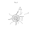
5 発光層
6 電子輸送層
8 第1の量子ドット
9 第1の発光層
10 第2の量子ドット
11 第2の発光層
12 コア部
13 シェル部
15 第1の界面活性剤
16 第2の界面活性剤
17 コア部
18 シェル部
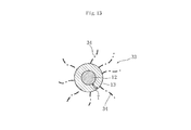
24 発光層
25 第1の発光層
26 第2の発光層
27 第1の量子ドット
30 発光層
31 第1の発光層
32 第2の発光層
33 第1の量子ドット
34 第3の界面活性剤
Claims (9)
- 発光層が正孔輸送層と電子輸送層との間に介在され、前記発光層に電流が注入されて発光する発光デバイスであって、
前記発光層が、コア部と該コア部を被覆するシェル部とを有するコア−シェル構造を備えた第1及び第2の発光層を含む積層構造とされ、
前記第1の発光層は、前記シェル部の厚みが前記シェル部の構成分子基準で3〜5モノレイヤーに形成された第1の量子ドットからなると共に、前記第2の発光層は、前記シェル部の厚みが前記シェル部の構成分子基準で3モノレイヤー未満に形成された第2の量子ドットからなり、
前記第1及び第2の量子ドットは、前記シェル部の表面が、正孔輸送性を有する第1の界面活性剤と電子輸送性を有する第2の界面活性剤の双方で被覆されると共に、
前記第1の発光層が前記電子輸送層側に配され、前記第2の発光層が前記正孔輸送層側に配されていることを特徴とする発光デバイス。 - 前記第1の界面活性剤は、前記コア部の価電子帯及び該価電子帯の励起準位とトンネル共鳴するような価電子帯を有していることを特徴とする請求項1記載の発光デバイス。
- 前記第2の界面活性剤は、前記コア部の伝導帯及び該伝導帯の励起準位とトンネル共鳴するような伝導帯を有していることを特徴とする請求項1又は請求項2記載の発光デバイス。
- 発光層が正孔輸送層と電子輸送層との間に介在され、前記発光層に電流が注入されて発光する発光デバイスであって、
前記発光層が、コア部と該コア部を被覆するシェル部とを有するコア−シェル構造を備えた第1及び第2の発光層を含む積層構造とされ、
前記第1の発光層は、前記シェル部の厚みが前記シェル部の構成分子基準で3〜5モノレイヤーに形成された第1の量子ドットからなると共に、前記第2の発光層は、前記シェル部の厚みが前記シェル部の構成分子基準で3モノレイヤー未満に形成された第2の量子ドットからなり、
前記第2の量子ドットは、前記シェル部の表面が、正孔輸送性を有する第1の界面活性剤及び電子輸送性を有する第2の界面活性剤の双方で被覆されると共に、
前記第1の量子ドットは、前記シェル部の表面が、前記第2の界面活性剤で被覆され、
前記第1の発光層が前記電子輸送層側に配され、前記第2の発光層が前記正孔輸送層側に配されていることを特徴とする発光デバイス。 - 前記第2の界面活性剤は、前記コア部の伝導帯及び該伝導帯の励起準位とトンネル共鳴するような伝導帯を有していることを特徴とする請求項4記載の発光デバイス。
- 発光層が正孔輸送層と電子輸送層との間に介在され、前記発光層に電流が注入されて発光する発光デバイスであって、
前記発光層が、コア部と該コア部を被覆するシェル部とを有するコア−シェル構造を備えた第1及び第2の発光層を含む積層構造とされ、
前記第1の発光層は、前記シェル部の厚みが前記シェル部の構成分子基準で3〜5モノレイヤーに形成された第1の量子ドットからなると共に、前記第2の発光層は、前記シェル部の厚みが前記シェル部の構成分子基準で3モノレイヤー未満に形成された第2の量子ドットからなり、
前記第2の量子ドットは、前記シェル部の表面が、正孔輸送性を有する第1の界面活性剤及び電子輸送性を有する第2の界面活性剤の双方で表面が被覆されると共に、
前記第1の量子ドットは、前記シェル部の表面が、絶縁性を有する第3の界面活性剤で被覆され、
前記第1の発光層が前記電子輸送層側に配され、前記第2の発光層が前記正孔輸送層側に配されていることを特徴とする発光デバイス。 - 前記第1の発光層の厚みは、前記第1の量子ドットの粒径基準で0.5〜2モノレイヤーであることを特徴とする請求項6記載の発光デバイス。
- 前記第1及び第2の量子ドットの各シェル部は、真空準位を基準にした価電子帯のエネルギー準位が、前記コア部の価電子帯のエネルギー準位よりも低位にあることを特徴とする請求項1乃至請求項7のいずれかに記載の発光デバイス。
- 前記第1及び第2の量子ドットの各シェル部は、真空準位を基準にした価電子帯のエネルギー準位が、前記電子輸送層の価電子帯のエネルギー準位又は前記電子輸送層のHOMO準位よりも低位にあることを特徴とする請求項1乃至請求項8のいずれかに記載の発光デバイス。
Applications Claiming Priority (3)
| Application Number | Priority Date | Filing Date | Title |
|---|---|---|---|
| JP2013216635 | 2013-10-17 | ||
| JP2013216635 | 2013-10-17 | ||
| PCT/JP2014/077586 WO2015056750A1 (ja) | 2013-10-17 | 2014-10-16 | ナノ粒子材料、及び発光デバイス |
Publications (2)
| Publication Number | Publication Date |
|---|---|
| JPWO2015056750A1 JPWO2015056750A1 (ja) | 2017-03-09 |
| JP6233417B2 true JP6233417B2 (ja) | 2017-11-22 |
Family
ID=52828191
Family Applications (1)
| Application Number | Title | Priority Date | Filing Date |
|---|---|---|---|
| JP2015542660A Active JP6233417B2 (ja) | 2013-10-17 | 2014-10-16 | 発光デバイス |
Country Status (4)
| Country | Link |
|---|---|
| US (1) | US9722198B2 (ja) |
| JP (1) | JP6233417B2 (ja) |
| CN (1) | CN105684555B (ja) |
| WO (1) | WO2015056750A1 (ja) |
Cited By (3)
| Publication number | Priority date | Publication date | Assignee | Title |
|---|---|---|---|---|
| US11424425B2 (en) | 2019-10-07 | 2022-08-23 | Samsung Electronics Co., Ltd. | Electroluminescent device, and display device comprising thereof |
| US11495764B2 (en) | 2019-09-20 | 2022-11-08 | Samsung Electronics Co., Ltd. | Electroluminescent device, and display device comprising same |
| US11758663B2 (en) | 2019-03-28 | 2023-09-12 | Samsung Display Co., Ltd. | Display device |
Families Citing this family (57)
| Publication number | Priority date | Publication date | Assignee | Title |
|---|---|---|---|---|
| US10608184B2 (en) * | 2012-12-03 | 2020-03-31 | The University Of Akron | Organic polymer photo device with broadband response and increased photo-responsitivity |
| US9574135B2 (en) * | 2013-08-22 | 2017-02-21 | Nanoco Technologies Ltd. | Gas phase enhancement of emission color quality in solid state LEDs |
| CN105552244B (zh) * | 2016-02-17 | 2018-09-11 | 京东方科技集团股份有限公司 | 一种发光器件及其制备方法、显示装置 |
| EP3419070B1 (en) * | 2016-02-18 | 2022-04-13 | BOE Technology Group Co., Ltd. | Quantum dot light-emitting device |
| US10741719B2 (en) * | 2016-03-12 | 2020-08-11 | Faquir Chand Jain | Quantum dot channel (QDC) quantum dot gate transistors, memories and other devices |
| KR102607451B1 (ko) * | 2016-03-15 | 2023-11-28 | 삼성디스플레이 주식회사 | 발광 소자 및 이를 포함하는 표시 장치 |
| US10700236B2 (en) | 2016-03-17 | 2020-06-30 | Apple Inc. | Quantum dot spacing for high efficiency quantum dot LED displays |
| US9768404B1 (en) * | 2016-03-17 | 2017-09-19 | Apple Inc. | Quantum dot spacing for high efficiency quantum dot LED displays |
| CN108389982B (zh) * | 2016-08-23 | 2020-03-27 | 苏州星烁纳米科技有限公司 | 发光二极管装置及显示装置 |
| CN106784349B (zh) * | 2016-12-21 | 2020-02-07 | Tcl集团股份有限公司 | 一种能级势垒高度连续变化的量子点固态膜及其制备方法 |
| CN106848085A (zh) * | 2017-04-07 | 2017-06-13 | 京东方科技集团股份有限公司 | Qled器件及其制作方法、qled显示面板和qled显示装置 |
| CN107342367A (zh) * | 2017-06-28 | 2017-11-10 | 深圳市华星光电技术有限公司 | 量子点电致发光器件及其制作方法 |
| CN107359264B (zh) * | 2017-08-03 | 2019-12-31 | 青岛海信电器股份有限公司 | 一种qled、制备方法及显示装置 |
| CN109494307B (zh) * | 2017-09-12 | 2021-06-08 | 乐金显示有限公司 | 量子点发光二极管以及包括该量子点发光二极管的量子点显示设备 |
| KR102374223B1 (ko) * | 2017-09-19 | 2022-03-14 | 엘지디스플레이 주식회사 | 다중 발광 양자점과 이를 포함하는 양자점 필름, 엘이디 패키지, 발광다이오드 및 표시장치 |
| CN109935725B (zh) * | 2017-12-15 | 2020-08-14 | Tcl科技集团股份有限公司 | 量子点发光二极管及其制备方法和应用 |
| CN109960078A (zh) * | 2017-12-26 | 2019-07-02 | 优美特创新材料股份有限公司 | 背光模块 |
| JP6965764B2 (ja) * | 2018-01-18 | 2021-11-10 | 富士通株式会社 | 光検出器及びその製造方法、撮像装置 |
| CN108281530A (zh) * | 2018-01-31 | 2018-07-13 | 惠州市华星光电技术有限公司 | 一种量子点led、背光模块及显示装置 |
| WO2019171503A1 (ja) * | 2018-03-07 | 2019-09-12 | シャープ株式会社 | 発光デバイス、発光デバイスの製造方法、発光デバイスの製造装置 |
| EP3544074A3 (en) * | 2018-03-19 | 2019-11-06 | Samsung Electronics Co., Ltd. | Electroluminescent device, and display device comprising thereof |
| US11737301B2 (en) | 2018-03-19 | 2023-08-22 | Samsung Electronics Co., Ltd. | Electroluminescent device, and display device comprising thereof |
| CN111903191A (zh) * | 2018-03-30 | 2020-11-06 | 夏普株式会社 | 发光元件、发光设备以及发光元件的制造装置 |
| CN108550707B (zh) | 2018-04-12 | 2022-11-08 | 京东方科技集团股份有限公司 | 量子点发光二极管、液晶显示设备 |
| CN108630817B (zh) * | 2018-05-07 | 2019-11-29 | 河南大学 | 一种适用于照明应用的量子点发光二极管及其制备方法 |
| CN112425265A (zh) * | 2018-07-24 | 2021-02-26 | 夏普株式会社 | 发光装置、发光装置的制造方法、发光装置的制造装置 |
| CN109301076B (zh) * | 2018-09-17 | 2020-08-28 | 南昌航空大学 | 单色量子点发光二极管的结构及制备方法 |
| KR102581900B1 (ko) * | 2018-10-12 | 2023-09-21 | 삼성전자주식회사 | 발광 소자와 이를 포함한 표시 장치 |
| KR20200049980A (ko) * | 2018-10-30 | 2020-05-11 | 엘지디스플레이 주식회사 | 양자점 필름, 엘이디 패키지, 발광다이오드 및 표시장치 |
| JP2020072089A (ja) * | 2018-10-30 | 2020-05-07 | 国立研究開発法人産業技術総合研究所 | 半導体粒子および電子デバイス |
| US20220013744A1 (en) * | 2018-10-30 | 2022-01-13 | Sharp Kabushiki Kaisha | Light-emitting element, method for manufacturing light-emitting element |
| CN109768178B (zh) * | 2019-01-22 | 2021-03-30 | 京东方科技集团股份有限公司 | 有机电致发光器件、显示基板、显示装置 |
| WO2020170371A1 (ja) * | 2019-02-20 | 2020-08-27 | シャープ株式会社 | 発光デバイスの製造方法 |
| JP7198688B2 (ja) * | 2019-03-04 | 2023-01-11 | シャープ株式会社 | ハイブリッド粒子、光電変換素子、感光体及び画像形成装置 |
| US20220158115A1 (en) * | 2019-03-04 | 2022-05-19 | Sharp Kabushiki Kaisha | Light-emitting element and display device |
| JP2020161369A (ja) * | 2019-03-27 | 2020-10-01 | 東洋インキScホールディングス株式会社 | 半導体微粒子組成物、及び電界発光素子 |
| US11271190B2 (en) * | 2019-04-26 | 2022-03-08 | Samsung Electronics Co., Ltd. | Light emitting device and display device including the same |
| WO2020245924A1 (ja) * | 2019-06-04 | 2020-12-10 | シャープ株式会社 | 発光素子、発光デバイス |
| US20220310960A1 (en) * | 2019-09-04 | 2022-09-29 | Sharp Kabushiki Kaisha | Light-emitting element, light-emitting device, and method for manufacturing light-emitting element |
| KR20210036435A (ko) * | 2019-09-25 | 2021-04-05 | 삼성디스플레이 주식회사 | 양자점 조성물, 발광 소자 및 이를 포함하는 표시 장치 |
| WO2021064822A1 (ja) * | 2019-09-30 | 2021-04-08 | シャープ株式会社 | 発光素子、発光デバイス |
| US11476434B2 (en) * | 2019-10-31 | 2022-10-18 | Samsung Electronics Co., Ltd. | Electroluminescent device and display device comprising thereof |
| JP2021125492A (ja) * | 2020-01-31 | 2021-08-30 | キヤノン株式会社 | 半導体装置、表示装置、撮像システム及び移動体 |
| US20230090605A1 (en) * | 2020-02-06 | 2023-03-23 | Sharp Kabushiki Kaisha | Method for producing light-emitting device, and light-emitting device |
| US20230053170A1 (en) * | 2020-02-06 | 2023-02-16 | Sharp Kabushiki Kaisha | Light-emitting device, and method for manufacturing light-emitting device |
| WO2021157020A1 (ja) * | 2020-02-06 | 2021-08-12 | シャープ株式会社 | 発光デバイスの製造方法 |
| KR20220003356A (ko) * | 2020-07-01 | 2022-01-10 | 삼성전자주식회사 | 발광 소자 및 이를 포함하는 표시 장치 |
| CN111952474B (zh) * | 2020-08-18 | 2023-11-03 | 福州大学 | 一种基于有机物聚合的量子点发光二极管及其制备方法 |
| CN112103393B (zh) * | 2020-09-18 | 2023-10-10 | 隆基绿能科技股份有限公司 | 等离子激元结构及钙钛矿光电器件 |
| KR20220043997A (ko) | 2020-09-28 | 2022-04-06 | 삼성디스플레이 주식회사 | 양자점 조성물 및 이를 이용한 발광 소자의 제조 방법 |
| WO2022079817A1 (ja) * | 2020-10-14 | 2022-04-21 | シャープ株式会社 | 発光素子 |
| CN114566598A (zh) * | 2020-11-27 | 2022-05-31 | 京东方科技集团股份有限公司 | 一种发光器件、显示装置和制作方法 |
| US20240081086A1 (en) * | 2020-12-22 | 2024-03-07 | Sharp Kabushiki Kaisha | Ligh-emitting element and light-emitting device |
| CN115835669A (zh) * | 2021-09-16 | 2023-03-21 | Tcl科技集团股份有限公司 | 量子点发光器件及显示装置 |
| WO2023044788A1 (zh) * | 2021-09-24 | 2023-03-30 | 京东方科技集团股份有限公司 | 量子点膜层、量子点发光器件及其制作方法 |
| CN115884615A (zh) * | 2021-09-26 | 2023-03-31 | Tcl科技集团股份有限公司 | 量子点发光器件和显示面板 |
| WO2023073783A1 (ja) * | 2021-10-25 | 2023-05-04 | シャープディスプレイテクノロジー株式会社 | 発光素子、発光素子の製造方法、表示装置 |
Family Cites Families (25)
| Publication number | Priority date | Publication date | Assignee | Title |
|---|---|---|---|---|
| GB2342651B (en) * | 1998-09-18 | 2001-10-17 | Massachusetts Inst Technology | Biological applications of semiconductor nanocrystals |
| JP2002184970A (ja) | 2000-12-15 | 2002-06-28 | Fujitsu Ltd | 量子ドットを含む半導体装置、その製造方法及び半導体レーザ装置 |
| US6819845B2 (en) * | 2001-08-02 | 2004-11-16 | Ultradots, Inc. | Optical devices with engineered nonlinear nanocomposite materials |
| JP2005502176A (ja) * | 2001-09-04 | 2005-01-20 | コーニンクレッカ フィリップス エレクトロニクス エヌ ヴィ | 量子ドットを有するエレクトロルミネセント装置 |
| US7205048B2 (en) * | 2001-09-17 | 2007-04-17 | Invitrogen Corporation | Functionalized fluorescent nanocrystal compositions and methods of making |
| US7645397B2 (en) | 2004-01-15 | 2010-01-12 | Nanosys, Inc. | Nanocrystal doped matrixes |
| JP4789809B2 (ja) | 2004-01-15 | 2011-10-12 | サムスン エレクトロニクス カンパニー リミテッド | ナノ結晶をドーピングしたマトリックス |
| WO2006093516A2 (en) * | 2004-06-22 | 2006-09-08 | The Regents Of The University Of California | Peptide-coated nanoparticles with graded shell compositions |
| JP2006185985A (ja) | 2004-12-27 | 2006-07-13 | Sony Corp | 発光デバイス及びその製造方法 |
| US7414294B2 (en) * | 2005-12-16 | 2008-08-19 | The Trustees Of Princeton University | Intermediate-band photosensitive device with quantum dots having tunneling barrier embedded in organic matrix |
| US8884511B2 (en) * | 2006-07-10 | 2014-11-11 | Hewlett-Packard Development Company, L.P. | Luminescent materials having nanocrystals exhibiting multi-modal energy level distributions |
| US7754329B2 (en) * | 2006-11-06 | 2010-07-13 | Evident Technologies, Inc. | Water-stable semiconductor nanocrystal complexes and methods of making same |
| JP2008214363A (ja) * | 2007-02-28 | 2008-09-18 | Canon Inc | ナノ粒子発光材料、これを用いた電界発光素子及びインク組成物、並びに表示装置 |
| US20080278063A1 (en) * | 2007-05-07 | 2008-11-13 | Cok Ronald S | Electroluminescent device having improved power distribution |
| US8361823B2 (en) * | 2007-06-29 | 2013-01-29 | Eastman Kodak Company | Light-emitting nanocomposite particles |
| JP2009087754A (ja) * | 2007-09-28 | 2009-04-23 | Dainippon Printing Co Ltd | 発光素子 |
| CN102576746B (zh) * | 2009-09-28 | 2015-05-13 | 株式会社村田制作所 | 纳米粒子材料和光电转换器件 |
| WO2011037042A1 (ja) | 2009-09-28 | 2011-03-31 | 株式会社 村田製作所 | ナノ粒子材料の製造方法、及びナノ粒子材料、並びに光電変換デバイス |
| JP2011076726A (ja) * | 2009-09-29 | 2011-04-14 | Hoya Corp | 電界発光素子およびその製造方法 |
| JP2011073726A (ja) * | 2009-09-30 | 2011-04-14 | Toppan Printing Co Ltd | ガラス基板枚葉トレイ段積み用パレット |
| JP2011252117A (ja) * | 2010-06-03 | 2011-12-15 | Sharp Corp | 半導体微粒子蛍光体、ならびにそれを用いた波長変換部材、発光装置および画像表示装置 |
| WO2012128173A1 (ja) * | 2011-03-24 | 2012-09-27 | 株式会社 村田製作所 | 発光デバイス、及び該発光デバイスの製造方法 |
| US9412905B2 (en) * | 2011-04-01 | 2016-08-09 | Najing Technology Corporation Limited | White light emitting device |
| JP2013157180A (ja) * | 2012-01-30 | 2013-08-15 | Murata Mfg Co Ltd | 量子ドット膜の製造方法、及び光電変換デバイス |
| WO2013157563A1 (ja) * | 2012-04-20 | 2013-10-24 | コニカミノルタ株式会社 | 有機エレクトロルミネッセンス素子 |
-
2014
- 2014-10-16 CN CN201480056589.5A patent/CN105684555B/zh active Active
- 2014-10-16 WO PCT/JP2014/077586 patent/WO2015056750A1/ja active Application Filing
- 2014-10-16 JP JP2015542660A patent/JP6233417B2/ja active Active
-
2016
- 2016-04-15 US US15/099,796 patent/US9722198B2/en active Active
Cited By (4)
| Publication number | Priority date | Publication date | Assignee | Title |
|---|---|---|---|---|
| US11758663B2 (en) | 2019-03-28 | 2023-09-12 | Samsung Display Co., Ltd. | Display device |
| US11495764B2 (en) | 2019-09-20 | 2022-11-08 | Samsung Electronics Co., Ltd. | Electroluminescent device, and display device comprising same |
| US11424425B2 (en) | 2019-10-07 | 2022-08-23 | Samsung Electronics Co., Ltd. | Electroluminescent device, and display device comprising thereof |
| US11758746B2 (en) | 2019-10-07 | 2023-09-12 | Samsung Electronics Co., Ltd. | Electroluminescent device, and display device comprising thereof |
Also Published As
| Publication number | Publication date |
|---|---|
| CN105684555A (zh) | 2016-06-15 |
| US9722198B2 (en) | 2017-08-01 |
| CN105684555B (zh) | 2017-06-23 |
| JPWO2015056750A1 (ja) | 2017-03-09 |
| WO2015056750A1 (ja) | 2015-04-23 |
| US20160233449A1 (en) | 2016-08-11 |
Similar Documents
| Publication | Publication Date | Title |
|---|---|---|
| JP6233417B2 (ja) | 発光デバイス | |
| JP6061112B2 (ja) | 発光デバイス | |
| JP6168372B2 (ja) | 発光デバイス、及び発光デバイスの製造方法 | |
| JP5828340B2 (ja) | 発光デバイス、及び該発光デバイスの製造方法 | |
| JP6710248B2 (ja) | 量子ドット発光ダイオードおよびこれを含む量子ドット発光装置 | |
| US9887375B2 (en) | Device including quantum dots and method for making same | |
| JP5370702B2 (ja) | 薄膜形成方法 | |
| JP5218927B2 (ja) | ナノ粒子材料及び光電変換デバイス | |
| CA2934970C (en) | Light emitting device including semiconductor nanocrystals | |
| JP5200296B2 (ja) | ナノ粒子材料の製造方法 | |
| US9093657B2 (en) | White light emitting devices | |
| US9722133B2 (en) | Methods for processing quantum dots and devices including quantum dots | |
| JP2008300270A (ja) | 発光素子 | |
| WO2014097878A1 (ja) | 発光デバイス、及び該発光デバイスの製造方法 | |
| KR20230021571A (ko) | 표면 개질된 양자점, 이의 제조 방법, 및 이를 포함하는 양자점-폴리머 복합체 또는 전자 소자 |
Legal Events
| Date | Code | Title | Description |
|---|---|---|---|
| A131 | Notification of reasons for refusal |
Free format text: JAPANESE INTERMEDIATE CODE: A131 Effective date: 20170303 |
|
| A521 | Request for written amendment filed |
Free format text: JAPANESE INTERMEDIATE CODE: A523 Effective date: 20170426 |
|
| TRDD | Decision of grant or rejection written | ||
| A01 | Written decision to grant a patent or to grant a registration (utility model) |
Free format text: JAPANESE INTERMEDIATE CODE: A01 Effective date: 20170926 |
|
| A61 | First payment of annual fees (during grant procedure) |
Free format text: JAPANESE INTERMEDIATE CODE: A61 Effective date: 20171009 |
|
| R150 | Certificate of patent or registration of utility model |
Ref document number: 6233417 Country of ref document: JP Free format text: JAPANESE INTERMEDIATE CODE: R150 |