WO2012115059A1 - 微細構造成形体および該微細構造成形体を備えた液晶表示装置 - Google Patents
微細構造成形体および該微細構造成形体を備えた液晶表示装置 Download PDFInfo
- Publication number
- WO2012115059A1 WO2012115059A1 PCT/JP2012/054018 JP2012054018W WO2012115059A1 WO 2012115059 A1 WO2012115059 A1 WO 2012115059A1 JP 2012054018 W JP2012054018 W JP 2012054018W WO 2012115059 A1 WO2012115059 A1 WO 2012115059A1
- Authority
- WO
- WIPO (PCT)
- Prior art keywords
- inorganic oxide
- oxide layer
- substrate
- ridge
- layer
- Prior art date
Links
Images


Classifications
-
- G—PHYSICS
- G02—OPTICS
- G02B—OPTICAL ELEMENTS, SYSTEMS OR APPARATUS
- G02B1/00—Optical elements characterised by the material of which they are made; Optical coatings for optical elements
- G02B1/10—Optical coatings produced by application to, or surface treatment of, optical elements
- G02B1/11—Anti-reflection coatings
- G02B1/118—Anti-reflection coatings having sub-optical wavelength surface structures designed to provide an enhanced transmittance, e.g. moth-eye structures
-
- G—PHYSICS
- G02—OPTICS
- G02B—OPTICAL ELEMENTS, SYSTEMS OR APPARATUS
- G02B5/00—Optical elements other than lenses
- G02B5/30—Polarising elements
- G02B5/3025—Polarisers, i.e. arrangements capable of producing a definite output polarisation state from an unpolarised input state
- G02B5/3058—Polarisers, i.e. arrangements capable of producing a definite output polarisation state from an unpolarised input state comprising electrically conductive elements, e.g. wire grids, conductive particles
-
- G—PHYSICS
- G02—OPTICS
- G02B—OPTICAL ELEMENTS, SYSTEMS OR APPARATUS
- G02B5/00—Optical elements other than lenses
- G02B5/30—Polarising elements
-
- B—PERFORMING OPERATIONS; TRANSPORTING
- B32—LAYERED PRODUCTS
- B32B—LAYERED PRODUCTS, i.e. PRODUCTS BUILT-UP OF STRATA OF FLAT OR NON-FLAT, e.g. CELLULAR OR HONEYCOMB, FORM
- B32B9/00—Layered products comprising a layer of a particular substance not covered by groups B32B11/00 - B32B29/00
-
- G—PHYSICS
- G02—OPTICS
- G02F—OPTICAL DEVICES OR ARRANGEMENTS FOR THE CONTROL OF LIGHT BY MODIFICATION OF THE OPTICAL PROPERTIES OF THE MEDIA OF THE ELEMENTS INVOLVED THEREIN; NON-LINEAR OPTICS; FREQUENCY-CHANGING OF LIGHT; OPTICAL LOGIC ELEMENTS; OPTICAL ANALOGUE/DIGITAL CONVERTERS
- G02F1/00—Devices or arrangements for the control of the intensity, colour, phase, polarisation or direction of light arriving from an independent light source, e.g. switching, gating or modulating; Non-linear optics
- G02F1/01—Devices or arrangements for the control of the intensity, colour, phase, polarisation or direction of light arriving from an independent light source, e.g. switching, gating or modulating; Non-linear optics for the control of the intensity, phase, polarisation or colour
- G02F1/13—Devices or arrangements for the control of the intensity, colour, phase, polarisation or direction of light arriving from an independent light source, e.g. switching, gating or modulating; Non-linear optics for the control of the intensity, phase, polarisation or colour based on liquid crystals, e.g. single liquid crystal display cells
- G02F1/133—Constructional arrangements; Operation of liquid crystal cells; Circuit arrangements
- G02F1/1333—Constructional arrangements; Manufacturing methods
- G02F1/1335—Structural association of cells with optical devices, e.g. polarisers or reflectors
- G02F1/133528—Polarisers
-
- C—CHEMISTRY; METALLURGY
- C09—DYES; PAINTS; POLISHES; NATURAL RESINS; ADHESIVES; COMPOSITIONS NOT OTHERWISE PROVIDED FOR; APPLICATIONS OF MATERIALS NOT OTHERWISE PROVIDED FOR
- C09K—MATERIALS FOR MISCELLANEOUS APPLICATIONS, NOT PROVIDED FOR ELSEWHERE
- C09K2323/00—Functional layers of liquid crystal optical display excluding electroactive liquid crystal layer characterised by chemical composition
- C09K2323/05—Bonding or intermediate layer characterised by chemical composition, e.g. sealant or spacer
- C09K2323/051—Inorganic, e.g. glass or silicon oxide
-
- G—PHYSICS
- G02—OPTICS
- G02F—OPTICAL DEVICES OR ARRANGEMENTS FOR THE CONTROL OF LIGHT BY MODIFICATION OF THE OPTICAL PROPERTIES OF THE MEDIA OF THE ELEMENTS INVOLVED THEREIN; NON-LINEAR OPTICS; FREQUENCY-CHANGING OF LIGHT; OPTICAL LOGIC ELEMENTS; OPTICAL ANALOGUE/DIGITAL CONVERTERS
- G02F1/00—Devices or arrangements for the control of the intensity, colour, phase, polarisation or direction of light arriving from an independent light source, e.g. switching, gating or modulating; Non-linear optics
- G02F1/01—Devices or arrangements for the control of the intensity, colour, phase, polarisation or direction of light arriving from an independent light source, e.g. switching, gating or modulating; Non-linear optics for the control of the intensity, phase, polarisation or colour
- G02F1/13—Devices or arrangements for the control of the intensity, colour, phase, polarisation or direction of light arriving from an independent light source, e.g. switching, gating or modulating; Non-linear optics for the control of the intensity, phase, polarisation or colour based on liquid crystals, e.g. single liquid crystal display cells
- G02F1/133—Constructional arrangements; Operation of liquid crystal cells; Circuit arrangements
- G02F1/1333—Constructional arrangements; Manufacturing methods
- G02F1/1335—Structural association of cells with optical devices, e.g. polarisers or reflectors
- G02F1/133528—Polarisers
- G02F1/133548—Wire-grid polarisers
-
- Y—GENERAL TAGGING OF NEW TECHNOLOGICAL DEVELOPMENTS; GENERAL TAGGING OF CROSS-SECTIONAL TECHNOLOGIES SPANNING OVER SEVERAL SECTIONS OF THE IPC; TECHNICAL SUBJECTS COVERED BY FORMER USPC CROSS-REFERENCE ART COLLECTIONS [XRACs] AND DIGESTS
- Y10—TECHNICAL SUBJECTS COVERED BY FORMER USPC
- Y10T—TECHNICAL SUBJECTS COVERED BY FORMER US CLASSIFICATION
- Y10T428/00—Stock material or miscellaneous articles
- Y10T428/24—Structurally defined web or sheet [e.g., overall dimension, etc.]
- Y10T428/24628—Nonplanar uniform thickness material
Definitions
- the present invention relates to a microstructured molded body such as a wire grid polarizer and an antireflection article, and a liquid crystal display device having the microstructured molded body.
- a wire grid type polarizer is known as a polarizer (also referred to as a polarization element or a polarization separation element) having polarization separation ability in the visible light region, which is used in an image display apparatus such as a liquid crystal display device, a rear projection television, or a front projector. It has been.
- antireflection articles such as antireflection films are known as members that are arranged on the surface of a display of an image display device and prevent external light from being reflected on the surface of the display.
- the wire grid polarizer has a structure in which a plurality of fine metal wires are arranged in parallel to each other on a light-transmitting substrate.
- the pitch of the fine metal wires is sufficiently shorter than the wavelength of the incident light, the component having an electric field vector orthogonal to the fine metal wires (that is, p-polarized light) in the incident light is transmitted and has an electric field vector parallel to the fine metal wires. (Ie s-polarized light) is reflected.
- the fine metal wires are very fine, so that the fine metal wires have low scratch resistance. For this reason, the fine metal wires are easily damaged by physical contact with the surface of the wire grid polarizer. In the wire grid type polarizer, even if the fine metal wire is slightly damaged, the performance of the wire grid type polarizer is affected.
- Patent Document 1 a protective film formed by a CVD method using tetraethoxysilane and oxygen gas.
- the protective film is formed by the CVD method, not the PVD method (sputtering method, vacuum deposition method, etc.) in which the high energy target component or evaporated particles collides with the target substrate, the metal thin wire and the protective film
- the adhesion of the protective film is poor, and the protective film is easily peeled off by physical contact or the like. Therefore, it is necessary to make the protective film relatively thick (about 200 nm).
- the protective film easily enters the gaps between the fine metal wires, and the gaps are filled with the protective film and become smaller, so that the optical characteristics of the wire grid polarizer are deteriorated. And if the optical characteristic of a wire grid type polarizer falls, the brightness
- an antireflection article there is an article having a structure in which fine protrusions called a moth-eye structure are formed at a predetermined pitch.
- the protrusions are very fine, so the scratch resistance of the protrusions is low and they are easily damaged by physical contact or the like. If the protrusion is damaged, it will lead to a decrease in the antireflection ability, and therefore development of a technique for suppressing the damage is desired.
- the present invention provides a microstructured molded body such as a wire grid polarizer and an antireflection article having sufficient scratch resistance and optical properties, and a liquid crystal display device including the microstructured molded body.
- the microstructured molded body of the present invention includes a substrate having convex portions formed on at least one surface at a pitch equal to or less than the wavelength of visible light, an inorganic oxide layer covering at least the top of the convex portions, and at least the inorganic
- the surface of the oxide layer has a fluorine-containing compound layer formed by treating with a fluorine-containing compound having a group reactive to an inorganic oxide, and the inorganic layer is coated on the top of the convex portion
- the oxide layer is characterized in that the thickness Ha is 30 nm or more and the ratio of the thickness Ha to the width Dat (Ha / Dat) is 1.0 or less.
- the inorganic oxide layer covers at least a part of the side surface of the convex portion, and the ratio (Da / Dat) between the thickness Da in the width direction of the inorganic oxide layer coated on the side surface and the width Dat is It is preferable that it is 0.25 or less.
- the fluorine-containing compound layer preferably has a thickness Hf of 1 to 30 nm.
- the fluorine-containing compound preferably has a hydrolyzable silyl group and a fluoroalkyl group (which may have an etheric oxygen atom between carbon-carbon atoms).
- the wire grid type polarizer of the present invention is a wire grid type polarizer comprising the microstructured compact of the present invention, wherein the convex portions are convex strips formed in parallel to each other, and at least the convex strips.
- the top portion is made of a metal layer, and a plurality of fine metal wires separated from each other are formed.
- the antireflection article of the present invention is characterized by comprising the microstructured molded body of the present invention.
- the antireflection article of the present invention is preferably composed of the microstructured molded body of the present invention, and the substrate preferably has a moth-eye structure.
- the substrate is preferably a light transmissive substrate.
- the liquid crystal display device of the present invention is characterized by having the microstructured molded body of the present invention.
- the liquid crystal display device of the present invention includes a liquid crystal panel having a liquid crystal layer sandwiched between a pair of substrates, a backlight unit, and the wire grid polarizer of the present invention.
- a fine structure molded body such as a wire grid polarizer and an antireflection article having sufficient scratch resistance and optical characteristics
- a liquid crystal display device including the fine structure molded body.
- FIG. 3 is a perspective view showing a light transmissive substrate of the wire grid polarizer of FIG. 2. It is a perspective view which shows the other example of a wire grid type polarizer.
- FIG. 5 is a perspective view showing a light transmissive substrate of the wire grid polarizer of FIG. 4. It is sectional drawing which shows an example of the liquid crystal display device of this invention. It is sectional drawing which shows an example of an antireflection article.
- the microstructured molded body of the present invention includes a substrate having convex portions formed on at least one surface at a pitch equal to or less than the wavelength of visible light, an inorganic oxide layer covering at least the top portions of the convex portions, and at least an inorganic oxide. And a fluorine-containing compound layer formed by treating the surface of the layer with a fluorine-containing compound having a group reactive to inorganic oxide, and the inorganic oxide layer coated on the top of the convex portion is The thickness Ha is 30 nm or more, and the ratio of the thickness Ha to the width Dat (Ha / Dat) is 1.0 or less.
- Examples of the microstructure molded body of the present invention include optical microstructure molded bodies such as wire grid polarizers and antireflection articles.
- the convex portion means a portion rising from the main surface of the substrate and extending in one direction.
- the convex portion may be made of the same material as that of the main surface portion of the substrate, or may be made of a material different from that of the main surface portion of the substrate.
- the convex portion is composed of a base made of the same material as that of the main surface of the substrate integrally with the main surface of the substrate, and an upper portion formed on the base and made of a material different from that of the main surface of the substrate. May be.
- the protrusions are protrusions extending in a direction along the surface direction of the substrate and formed in parallel to each other and at a predetermined pitch equal to or less than the wavelength of visible light; cones such as cones and pyramids, and frustums based on the cones (That is, a conical body obtained by removing a conical body that shares a vertex and is reduced in a similar manner), and protrusions formed at a predetermined pitch equal to or smaller than the wavelength of visible light.
- a wire grid polarizer has protrusions as protrusions
- an antireflection article has protrusions as protrusions composed of a cone and a frustum based on the cone.
- the pitch is formed between the width of the protrusion (the direction parallel to the main surface of the substrate and the length in the direction perpendicular to the length of the protrusion) and the adjacent protrusions. It is the total with the width of the groove to be made.
- a pitch is the distance between the bottom face centers of the closest protrusions.
- the shape of the cross section in the direction perpendicular to the length direction and the main surface of the substrate is substantially constant over the length direction of the ridges, and all of the cross-sectional shapes of the ridges are also substantially constant.
- the cross-sectional shape of the ridge include a shape having substantially the same width from the bottom (main surface of the substrate) to the top, or a shape in which the width gradually narrows from the bottom to the top, specifically, for example, A rectangle, a triangle, a trapezoid, etc. are mentioned.
- the cross-sectional shape may be a curved corner or side (side surface, upper surface (upper bottom surface)).
- the protrusions it is preferable that the shape of each protrusion is substantially constant. Further, the cross-sectional shape may be such that the corners and sides (side surfaces, upper surface (upper bottom surface)) are curved.
- the top means a portion where the highest cross-sectional shape is continuous in the length direction.
- the top of the ridge may be a surface or a line.
- a top part means the highest part of each protrusion.
- the top of the protrusion may be a surface or a point.
- the surface other than the top of the convex portion is referred to as a side surface.
- channel between two adjacent convex parts is considered not the surface of a convex part but the main surface of a board
- the substrate provided with the wire grid polarizer of the present invention comprises a light transmissive substrate and a plurality of fine metal wires arranged in parallel to each other on the light transmissive substrate.
- Examples include a substrate on which a fine metal wire constituting an upper portion of the ridge (hereinafter referred to as an upper portion of the ridge) is formed on the ridge base.
- At least the top of the ridges of the wire grid polarizer is made of a metal layer, thereby forming a plurality of fine metal wires separated from each other.
- the light transmissive substrate is light transmissive in the wavelength range of use of the wire grid polarizer.
- Examples of the material for the light-transmitting substrate include a photo-curing resin, a thermoplastic resin, and glass, and a photo-curing resin or a thermoplastic resin is preferable from the viewpoint that a protruding base can be formed by an imprint method to be described later.
- a photo-curing resin is particularly preferable from the viewpoint that the ridge base can be formed by the imprint method and that the heat resistance and durability are excellent.
- the photocurable resin a photocurable resin obtained by photocuring a photocurable composition that can be photocured by photoradical polymerization is preferable from the viewpoint of productivity.
- the light transmissive substrate may be a laminate.
- this laminated body what is provided with the surface layer which has a base material which consists of a base material which consists of a thermoplastic resin, glass etc., and a photocuring resin formed in the surface of this base material, for example is mentioned.
- the shape of the cross section in the direction perpendicular to the length direction and the main surface of the substrate is substantially constant over the length direction of the ridge base portion, and all of the cross-sectional shapes are also substantially constant in the plurality of ridge base portions. It is preferable.
- the cross-sectional shape of the ridge base is preferably a shape having substantially the same width from the bottom (main surface of the substrate) to the top of the ridge base, or a shape in which the width gradually narrows from the bottom to the top. Specific examples of the cross-sectional shape include a rectangle, a triangle, and a trapezoid.
- the cross-sectional shape may have a curved corner or side (side surface).
- the fine metal wires include those formed by patterning a metal layer made of a metal or a metal compound formed on the surface of a flat light-transmitting substrate.
- the fine metal wire formed by patterning becomes the protruding line of the substrate.
- a metal layer made of a metal or a metal compound is selectively formed.
- the ridge of the substrate is constituted by the ridge upper portion made of a fine metal wire and the ridge base portion of the light-transmitting substrate.
- the plurality of fine metal wires only need to be formed substantially in parallel, and may not be formed completely in parallel.
- the line which comprises each metal fine wire is the straight line which is most easy to express optical anisotropy in a plane, it may be a curve or a broken line in the range which an adjacent metal thin wire does not contact.
- the thin metal wire is composed of a metal layer extending in the length direction of the ridge base.
- the metal layer may be substantially continuous in the length direction and may cover at least a part of the surface of the ridge base as long as there are no interrupted parts other than fine defects.
- the metal layer may cover a part or all of the top of the ridge base, or cover the whole top of the ridge base and a part or all of the second side surface of the ridge base. May be.
- the metal layer may coat
- the top of the ridge base portion refers to a portion where the highest cross-sectional shape of the ridge base portion continues in the length direction.
- the top of the ridge base may be a surface or a line.
- the metal examples include simple metals, alloys, metals containing dopants or impurities, and the like. Specifically, aluminum, silver, chromium, magnesium, an aluminum alloy, a silver alloy, and the like can be given.
- the material for the fine metal wire is preferably aluminum, an aluminum-based alloy, silver, chromium, or magnesium from the viewpoint of high reflectivity with respect to visible light, low visible light absorption, and high conductivity, and aluminum or aluminum A base alloy is particularly preferable.
- An inorganic oxide layer is a layer which coat
- the inorganic oxide layer may cover at least a part of the two side surfaces of the ridge and the surface of the substrate between the ridges (flat portion between the ridges), but covers only the top of the ridge. However, sufficient effects (abrasion resistance and optical properties) can be obtained.
- the inorganic oxide layer is preferably formed such that voids (grooves) are formed between the ridges, that is, the gaps (grooves) between the ridges are not filled as much as possible.
- Examples of the material for the inorganic oxide layer include silicon oxide, zirconium oxide, tin oxide, titanium oxide, and aluminum oxide. From the point that the wire grid polarizer exhibits high transmittance in a short wavelength region, silicon oxide, oxide Zirconium or tin oxide is preferable, and silicon oxide is particularly preferable from the viewpoint of cost.
- the thickness Ha (in the height direction of the ridge) of the inorganic oxide layer covering the top of the ridge is 30 nm or more, and preferably 150 nm or less. Further, when the thickness Ha is 40 to 100 nm, the scratch resistance of the ridge is very excellent.
- Ha is the difference between the height of the top of the ridge based on the flat portion between the ridges and the height of the top of the inorganic oxide layer based on the flat portion between the ridges.
- the ratio (Ha / Dat) between the thickness Ha of the inorganic oxide layer covering the top of the ridge and the width Dat of the inorganic oxide layer covering the top of the ridge is 1.0 or less.
- the ratio (Ha / Dat) is preferably 0.4 to 0.8.
- the ratio (Ha / Dat) is 1.0 or less, the inorganic oxide layer covering the top of the ridge is not broken, and the scratch resistance of the ridge is improved.
- Dat is the width of the inorganic oxide layer that exists above the top of the ridge and covers the top, and when the width differs in the height direction of the inorganic oxide layer, the maximum width is It is.
- the inorganic oxide layer may cover two side surfaces of the ridge, or may cover one side surface of the two side surfaces. Furthermore, you may coat
- the ratio (Da / Dat) between the thickness Da in the width direction of the inorganic oxide layer covering the side surface and the aforementioned width Dat is preferably 0.25 or less.
- the ratio (Da / Dat) is more preferably 0.2 or less. When the ratio (Da / Dat) is 0.25 or less, sufficient gaps (grooves) are formed between the ridges, so that the optical characteristics of the wire grid polarizer are maintained well, and Abrasion resistance can be improved.
- Da is the thickness in the width direction of the inorganic oxide layer coated on the side surface at a half height (H ′ / 2) when the total height of the ridge is H ′. .
- the thicknesses Da on both side surfaces are coated so as to satisfy the ratio (Da / Dat) ⁇ 0.25.
- the fluorine-containing compound layer is a layer formed by treating the surface of the inorganic oxide layer with a fluorine-containing compound having a group reactive to the inorganic oxide, and covers the entire surface of the inorganic oxide layer.
- the fluorine-containing compound is a fluorine-containing compound having a hydrolyzable silyl group and a fluoroalkyl group, which will be described later
- the fluorine-containing compound layer is composed of a hydrolysis condensate of the fluorine-containing compound.
- Examples of groups reactive with inorganic oxides include silanol groups and hydrolyzable silyl groups.
- a hydrolyzable silyl group is particularly preferred from the viewpoint of reactivity with inorganic oxides.
- the hydrolyzable silyl group is a group in which an alkoxy group, an amino group, a halogen atom, or the like is bonded to a silicon atom, and is a group that can be cross-linked by forming a siloxane bond by hydrolysis.
- a trialkoxysilyl group, an alkyl dialkoxysilyl group and the like are preferable.
- fluorine-containing compound a hydrolyzable silyl group and a fluoroalkyl group (which may have an etheric oxygen atom between carbon-carbon atoms) from the viewpoint of reactivity with inorganic oxides and a low dynamic friction coefficient.
- Fluorine-containing compounds having are preferred.
- the dynamic friction coefficient of the fluorine-containing compound layer is preferably 0.2 or less, more preferably 0.15 or less from the viewpoint of scratch resistance.
- the dynamic friction coefficient of the fluorine-containing compound layer is measured according to ASTM D 1894.
- Examples of the method for producing the wire grid polarizer of the present invention include the following method ( ⁇ ) and method ( ⁇ ) depending on the method of forming the fine metal wire.
- (I) A step of forming a metal layer on the surface of a flat light-transmitting substrate and patterning the metal layer to form a plurality of fine metal wires arranged in parallel with each other at a predetermined pitch, thereby producing the substrate.
- (II) A step of forming an inorganic oxide layer by vapor-depositing an inorganic oxide on the substrate on which the fine metal wires are formed.
- III A step of forming the fluorine-containing compound layer by treating the surface of the inorganic oxide layer with a fluorine-containing compound having a group reactive to the inorganic oxide. In the case of the method ( ⁇ ), the fine metal wires formed in the step (I) become the ridges of the substrate.
- II) A step of forming an inorganic oxide layer by vapor-depositing an inorganic oxide on the substrate on which the fine metal wires are formed.
- (III) A step of forming the fluorine-containing compound layer by treating the surface of the inorganic oxide layer with a fluorine-containing compound having a group reactive to the inorganic oxide.
- the ridge of the substrate is constituted by the ridge base of the light-transmitting substrate and the fine metal wire (upper ridge).
- the fine metal wire is formed by forming a metal layer on the surface of a flat light-transmitting substrate and patterning the metal layer.
- An example of the method for forming the metal layer is a vapor deposition method.
- the vapor deposition method include a PVD method or a CVD method. From the viewpoint of adhesion between the light-transmitting substrate and the fine metal wire and the surface roughness of the fine metal wire, the PVD method (vacuum vapor deposition method, sputtering method, ion plating method). Etc.) is preferable, and the vacuum evaporation method is particularly preferable from the viewpoint of cost.
- the patterning is performed by forming a resist pattern on the surface of the metal layer, etching the resist pattern as a mask to remove an excess metal layer, and then removing the resist pattern.
- the inorganic oxide layer is formed by vapor-depositing an inorganic oxide on the substrate on the side where the fine metal wires are formed.
- Examples of the vapor deposition method include a PVD method or a CVD method. From the viewpoint of adhesion between a fine metal wire and an inorganic oxide layer and surface roughness, a PVD method (vacuum vapor deposition method, sputtering method, ion plating method, etc.) is used. A sputtering method is preferable, and a sputtering method is particularly preferable.
- the thickness Ha and the width Dat of the formed inorganic oxide layer can be controlled by adjusting the sputtering processing time. The width Dat also depends on the width and height of the ridge, the shape of the top of the ridge, the pitch, and the like.
- the thickness Ha of the inorganic oxide layer covering the top of the ridge is preferably 30 nm or more by appropriately adjusting the sputter processing time, the width and height of the ridge, the form of the top of the ridge, the pitch, etc. Can be controlled to 150 nm or less and the ratio (Ha / Dat) to 1.0 or less.
- the fluorine-containing compound layer is formed by treating the surface of the inorganic oxide layer with a fluorine-containing compound having a group reactive to the inorganic oxide.
- the following step (i) can be performed because a uniform and thin fluorine-containing compound layer can be formed. It is preferable to go through (iii).
- (I) The process of immersing the board
- (Ii) A step of rinsing the substrate with a solvent after lifting the substrate from the diluted solution of the fluorine-containing compound.
- (Iii) A step of rinsing the substrate and placing it under a constant temperature and humidity condition to hydrolyze and condense a hydrolyzable silyl group to form a fluorine-containing compound layer.
- the degree of condensation between the fluorine-containing compound layer and the inorganic oxide layer can be controlled, for example, by adjusting the concentration of the diluted solution used in step (i), the constant temperature and humidity conditions, and the time.
- Examples of the method for producing a light transmissive substrate include imprint methods (light imprint method, thermal imprint method), lithography methods, and the like.
- the imprinting method is preferable from the viewpoint of making it possible, and the optical imprinting method is particularly preferable from the point that the protruding strip base can be formed with higher productivity and the groove of the mold can be accurately transferred.
- a mold in which a plurality of grooves are formed in parallel with each other at a predetermined pitch by a combination of electron beam drawing and etching is used. This is a method of transferring to a photocurable composition applied on the surface and simultaneously photocuring the photocurable composition.
- the production of the light transmissive substrate by the optical imprint method is preferably performed through the following steps (i) to (iv).
- Radiation (ultraviolet ray, electron beam, etc.) is applied to the photocurable composition while the mold is pressed against the photocurable composition to cure the photocurable composition and to have a plurality of ridge bases corresponding to the grooves of the mold.
- Producing a light-transmitting substrate (Iv) A step of separating the mold from the light transmissive substrate.
- the production of the light-transmitting substrate by the thermal imprint method is preferably performed through the following steps (i) to (iii).
- Examples of the mold material used in the imprint method include silicon, nickel, quartz glass, and resin, and quartz glass or resin is preferable from the viewpoint of transfer accuracy.
- Examples of the resin include a fluorine-based resin (ethylene-tetrafluoroethylene copolymer, etc.), a cyclic olefin, a silicone resin, an epoxy resin, an acrylic resin, and the like. From the viewpoint of mold accuracy, a photocurable acrylic resin is preferable. .
- the resin mold preferably has an inorganic film having a thickness of 2 to 10 nm on the surface from the viewpoint of repeated transfer durability.
- As the inorganic film an oxide film such as silicon oxide, titanium oxide, and aluminum oxide is preferable.
- the imprint method can be performed by a single wafer method, and when a film is used as the substrate, the imprint method can be performed by a roll-to-roll method.
- the fine metal wire is formed by selectively depositing a metal or a metal compound on the surface of the ridge base portion of the light-transmitting substrate.
- the vapor deposition method examples include a PVD method or a CVD method, and a vacuum vapor deposition method, a sputtering method, or an ion plating method is preferable, and a vacuum vapor deposition method is particularly preferable.
- the vapor deposition method the oblique vapor deposition method by the vacuum vapor deposition method is most preferable because the incident direction of the evaporated particles with respect to the light-transmitting substrate can be controlled and a metal or a metal compound can be selectively deposited on the surface of the ridge.
- Steps (II) to (III) may be performed in the same manner as steps (II) to (III) in method ( ⁇ ).
- each dimension in this invention measures each dimension about arbitrary 5 places in the transmission electron microscope (TEM) image of the cross section of a wire grid type polarizer, and is taken as the average value.
- TEM transmission electron microscope
- FIG. 1 is a cross-sectional view showing a first embodiment of a wire grid polarizer of the present invention.
- the wire grid polarizer 1 has a flat light-transmitting substrate 10 and a rectangular cross-section formed on the surface of the light-transmitting substrate 10 at a predetermined pitch Pp parallel to each other and not more than the wavelength of visible light.
- the fluorine-containing compound layer 32 is provided.
- the inorganic oxide layer 30 includes the two side surfaces of the ridge 50 and the top portion 52 sandwiched between them, and the flat portion 13 of the substrate between the ridges 50. In this case, the inorganic oxide layer may cover only the top of the ridge, and even in that case, excellent scratch resistance and optical characteristics are sufficiently exhibited.
- Pp is the sum of the width Dm of the ridges 50 and the width of the grooves 14 formed between the ridges 50.
- Pp is not more than the wavelength of visible light and is preferably 30 to 300 nm, more preferably 50 to 200 nm.
- Pp is 300 nm or less, a high s-polarized reflectance is exhibited, and a high degree of polarization is exhibited even in a short wavelength region of about 400 nm. Moreover, the coloring phenomenon by diffraction is suppressed. Moreover, if Pp is 30 nm or more, high transmittance is exhibited.
- the ratio of Dm to Pp is preferably 0.1 to 0.7, and more preferably 0.25 to 0.55.
- Dm / Pp is 0.1 or more, a high degree of polarization is exhibited.
- Dm is preferably 10 to 100 nm from the viewpoint of easily forming the fine metal wire 20.
- the thickness of the inorganic oxide layer 30 covering the side surface of the ridge 50 (width direction of the ridge 50) Da and the thickness of the fluorine-containing compound layer 32 covering the inorganic oxide layer 30 (width direction of the ridge 50) ) The ratio ((Da + Df) / (Pp-Dm)) of the sum (Da + Df) to Df and the width (Pp-Dm) of the groove 14 is preferably 0.4 or less, and preferably 0.01 to 0.3 More preferred. If (Da + Df) / (Pp ⁇ Dm) is 0.4 or less, a sufficient gap is formed in the groove 14 and the optical characteristics become better.
- the thickness Ha (in the height direction of the ridge 50) Ha of the inorganic oxide layer 30 covering the top 52 of the ridge 50 is 30 nm or more. Further, the ratio (Ha / Dat) between the thickness Ha of the inorganic oxide layer 30 covering the top portion 52 of the ridge 50 and the width Dat of the inorganic oxide layer 30 is 1.0 or less as described above. . The ratio (Da / Dat) between the thickness Da of the inorganic oxide layer 30 covering the side surfaces of the ridges 50 (width direction of the ridges 50) and the aforementioned width Dat is 0.25 or less as described above. Is preferred.
- the height Hm of the ridge 50 composed of the fine metal wire 20 is preferably 50 to 500 nm, and more preferably 100 to 300 nm.
- Hm is 50 nm or more, the polarization separation ability is sufficiently high. If Hm is 500 nm or less, the chromatic dispersion is small. Further, when Hm is 100 to 300 nm, the fine metal wires 20 are easily formed.
- the thickness (the height direction of the protrusion 50) Hf of the fluorine-containing compound layer 32 covering the inorganic oxide layer 30 covering the top of the protrusion 50 is preferably 1 to 30 nm, and more preferably 1 to 20 nm. If Hf is 1 nm or more, the scratch resistance is sufficiently high. If Hf is 30 nm or less, it is easy to form a uniform and thin fluorine-containing compound layer 32.
- the thickness Hs of the light transmissive substrate 10 is preferably 0.5 to 1000 ⁇ m, and more preferably 1 to 200 ⁇ m.
- the wire grid polarizer 1 can be manufactured by the method ( ⁇ ) described above.
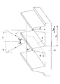
- FIG. 2 is a cross-sectional view showing a second embodiment of the wire grid polarizer of the present invention.
- a plurality of ridges 50 having a rectangular cross-sectional shape are parallel to each other through the flat portion 13 of the groove 14 formed between the ridges 50, and have a predetermined wavelength less than the wavelength of visible light.
- the ridge 50 is formed on the ridge base 12 of the light-transmitting substrate 10 as the ridge 50, and the metal fine wire forming the ridge upper portion. And 20. Further, the ridge base 12 is made of the same material as that of the light transmissive substrate 10.
- Pp is the total of the width Dp of the ridge base 12 and the width of the groove 14 formed between the ridges 50.
- Pp is not more than the wavelength of visible light and is preferably 30 to 300 nm, more preferably 50 to 200 nm.
- Pp is 300 nm or less, a high s-polarized reflectance is exhibited, and a high degree of polarization is exhibited even in a short wavelength region of about 400 nm. Moreover, the coloring phenomenon by diffraction is suppressed. Moreover, if Pp is 30 nm or more, high transmittance is exhibited.
- the ratio of Dp to Pp is preferably 0.1 to 0.7, and more preferably 0.25 to 0.55. If Dp / Pp is 0.1 or more, a high degree of polarization is exhibited. By setting Dp / Pp to 0.7 or less, coloring of transmitted light due to interference can be suppressed. Dp is preferably 10 to 100 nm from the viewpoint of easily forming a metal layer by vapor deposition.
- the width Dm of the fine metal wire 20 is preferably 10 to 100 nm, and more preferably 20 to 80 nm. If Dm is 10 nm or more, the polarization separation ability is sufficiently high. If Dm is 100 nm or less, the transmittance is sufficiently high.
- the thickness of the inorganic oxide layer 30 covering the side surface of the ridge 50 (width direction of the ridge 50) Da and the thickness of the fluorine-containing compound layer 32 covering the inorganic oxide layer 30 (width direction of the ridge 50) ) The ratio ((Da + Df) / (Pp-Dp)) of the sum (Da + Df) to Df and the width (Pp-Dp) of the groove 14 is preferably 0.4 or less, and preferably 0.01 to 0.3 More preferred. If (Da + Df) / (Pp ⁇ Dp) is 0.4 or less, a sufficient gap is formed in the groove 14 and the optical characteristics become better.
- the height Hp of the ridge base 12 is preferably 50 to 500 nm, and more preferably 100 to 400 nm. If Hp is 50 nm or more, the polarization separation ability is sufficiently high. If Hp is 500 nm or less, the wavelength dispersion of transmittance can be reduced. If Hp is 50 to 500 nm, a metal layer can be easily formed by vapor deposition.
- the height Hm of the fine metal wire 20 is preferably 15 to 500 nm, and more preferably 15 to 300 nm. If Hm is 15 nm or more, the polarization separation ability is sufficiently high. If Hm is 500 nm or less, the wavelength dispersion of the transmittance becomes small. Further, when Hm is 15 to 300 nm, it is easy to form a metal layer.
- the thickness Ha (in the height direction of the ridge 50) Ha of the inorganic oxide layer 30 covering the top 52 of the ridge 50 is 30 nm or more.
- the ratio (Ha / Dat) between the thickness Ha of the inorganic oxide layer 30 covering the top 52 of the ridge 50 and the width Dat of the inorganic oxide layer 30 covering the top 52 of the ridge 50 is as described above.
- the ratio (Da / Dat) between the thickness Da of the inorganic oxide layer 30 covering the side surfaces of the ridges 50 (width direction of the ridges 50) and the aforementioned width Dat is 0.25 or less as described above. Is preferred.
- Da is the thickness in the width direction of the inorganic oxide layer coated on the side surface at the half height (H ′ / 2). It is. In the illustrated example, Da is constant in the height direction, but may not be constant.
- the thickness (the height direction of the protrusion 50) Hf of the fluorine-containing compound layer 32 covering the inorganic oxide layer 30 covering the top of the protrusion 50 is preferably 1 to 30 nm, and more preferably 1 to 20 nm. If Hf is 1 nm or more, the scratch resistance is sufficiently high. If Hf is 30 nm or less, it is easy to form a uniform and thin fluorine-containing compound layer 32.
- the thickness Hs of the light transmissive substrate 10 is preferably 0.5 to 1000 ⁇ m, and more preferably 1 to 200 ⁇ m.
- the wire grid polarizer 2 can be manufactured by the method ( ⁇ ) described above.
- the fine metal wire 20 is substantially orthogonal to the length direction L of the ridge base 12 and 20 on the second side surface 18 side with respect to the height direction H of the ridge base 12.
- the metal or metal compound from a direction V2 constituting the ⁇ 50 ° angle theta L the amount of deposition can be formed by depositing under the condition that the 15-100 nm.
- the condition that the deposition amount is 15 to 100 nm is a metal formed by depositing a metal or a metal compound on the surface of a flat portion where the ridge base is not formed when the coating layer is formed on the ridge base.
- the conditions are such that the layer thickness t is 15 to 100 nm.
- Angle theta L can be adjusted by using the following vapor deposition apparatus.
- the vapor deposition apparatus which can change the inclination of the transparent substrate 10 arrange
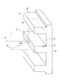
- FIG. 4 is a perspective view showing a third embodiment of the wire grid polarizer of the present invention.
- the wire grid polarizer 3 has a plurality of ridges 50 that transmit light at a predetermined pitch Pp parallel to each other and not more than the wavelength of visible light through the flat portions 13 of the grooves 14 formed between the ridges 50.
- the substrate formed on the surface of the conductive substrate 10; the side surface and top 52 of the ridge 50, and the flat portion 13 of the substrate between the ridges 50, so that a gap is formed in the groove 14 between the ridges 50.
- the wire grid type polarizer 3 of 3rd Embodiment is the metal strip 20 which is formed on the convex base 12 and this convex base 12 of the light-transmitting board
- the cross-sectional shape of the ridge 50 is a trapezoid. Further, the upper base of the trapezoid is curved.
- the ridge base 12 is made of the same material as that of the light transmissive substrate 10.
- the fine metal wire 20 includes a first metal layer 22 that covers the entire first side surface 16 of the ridge base 12, and a first metal layer on the top 19 side of the half of the height of the ridge base 12. 22 and the second metal layer 24 covering at least the top 19 of the ridge base 12.
- Pp is the sum of the width Dpb of the bottom of the ridge base 12 and the width of the flat portion 13 of the groove 14 formed between the ridges 50.
- Pp is not more than the wavelength of visible light, preferably 30 to 300 nm, more preferably 50 to 250 nm.
- Pp is 300 nm or less, a high surface s-polarized reflectance is exhibited, and a high degree of polarization is exhibited even in a short wavelength region of about 400 nm.
- Pp is 30 nm or more, high transmittance is exhibited.
- the ratio of Dpb to Pp is preferably 0.1 to 0.7, and more preferably 0.25 to 0.55.
- Dpb / Pp is 0.1 or more, a high degree of polarization is exhibited.
- Dpb is preferably 10 to 100 nm from the viewpoint of easily forming each layer by vapor deposition.
- the width Dpt of the top 19 of the ridge base 12 is preferably less than or equal to half of Dpb, more preferably 40 nm or less, and even more preferably 20 nm or less. If Dpt is less than or equal to half of Dpb, the p-polarized light transmittance is higher and the angle dependency is sufficiently low.
- the maximum value Dm1 of the thickness (in the width direction of the ridge base 12) from the half of the height of the ridge base 12 to the top 19 of the fine metal wire 20 (width direction of the ridge base 12) is 80 nm or less. It is preferably 20 to 75 nm, more preferably 35 to 55 nm, and particularly preferably 40 to 50 nm. If Dm1 is 20 nm or more, the surface s-polarized reflectance is sufficiently high. If Dm1 is 80 nm or less, the p-polarized light transmittance is sufficiently high.
- the maximum value Dm2 of the thin metal wire 20 from the position half the height of the ridge base 12 to the bottom (lower half of the ridge base 12) (in the width direction of the ridge base 12) is 4 to 25 nm. Preferably, 5 to 22 nm is more preferable. If Dm2 is 4 nm or more, the back surface s-polarized reflectance is sufficiently low. If Dm2 is 25 nm or less, the p-polarized light transmittance is sufficiently high.
- the ratio (Dm1 / (Pp-Dpb)) between Dm1 and the width of the groove 14 (Pp-Dpb) is preferably 0.2 to 0.5.
- Dm1 / (Pp-Dpb) is 0.2 or more, the s-polarized light transmittance is lowered, the polarization separation ability is sufficiently high, and the chromatic dispersion is small.
- Dm1 / (Pp-Dpb) is 0.5 or less, high p-polarized light transmittance is exhibited.
- the ratio of Dm1 to Dm2 is preferably 2.5 to 10, and more preferably 3 to 8. If Dm1 / Dm2 is 2.5 or more, the polarization separation ability is sufficiently high, and the chromatic dispersion is small. When Dm1 / Dm2 is 10 or less, high p-polarized light transmittance is exhibited.
- the thickness of the inorganic oxide layer 30 covering the side surface of the ridge 50 (width direction of the ridge 50) Da and the thickness of the fluorine-containing compound layer 32 covering the inorganic oxide layer 30 (width direction of the ridge 50) ) The ratio ((Da + Df) / (Pp-Dpb)) of the sum (Da + Df) to Df and the width (Pp-Dpb) of the groove 14 is preferably 0.4 or less, and preferably 0.01 to 0.3 More preferred. When (Da + Df) / (Pp ⁇ Dpb) is 0.4 or less, a sufficient gap is formed in the groove 14 and the optical characteristics are improved.
- the height Hp of the ridge base 12 is preferably 120 to 1000 nm. If Hp is 120 nm or more, the polarization separation ability is sufficiently high. If Hp is 1000 nm or less, the ridge base 12 is easily formed. If Hp is 300 nm or less, the chromatic dispersion is small. Further, when Hp is 120 to 300 nm, the fine metal wires 20 are easily formed by vapor deposition.
- Hm2 / Hp is preferably 0.8 to 1, more preferably 0.9 to 1. . If Hm2 / Hp is 1 or less, the polarization separation ability is improved. If Hm2 / Hp is 0.8 or more, the back surface s-polarized reflectance is sufficiently low.
- Hm1 / Hp is preferably 0.05 to 0.7, preferably 0.1 to 0.5 is more preferable. If Hm1 / Hp is 0.7 or less, the back surface s-polarized reflectance is sufficiently low. If Hm1 / Hp is 0.05 or more, the surface s-polarized reflectance is sufficiently high.
- the thickness Ha (in the height direction of the ridge 50) Ha of the inorganic oxide layer 30 covering the top 52 of the ridge 50 is 30 nm or more. Further, the ratio (Ha / Dat) between the thickness Ha of the inorganic oxide layer 30 covering the top portion 52 of the ridge 50 and the width Dat of the inorganic oxide layer 30 is 1.0 or less as described above. . The ratio (Da / Dat) between the thickness Da of the inorganic oxide layer 30 covering the side surfaces of the ridges 50 (width direction of the ridges 50) and the aforementioned width Dat is 0.25 or less as described above. Is preferred.
- the total height of the ridges H ′ Hm1 + Hp
- Da is the thickness in the width direction of the inorganic oxide layer coated on the side surface at the half height (H ′ / 2). It is. In the illustrated example, Da is constant in the height direction, but may not be constant.
- the thickness (in the height direction of the ridge 50) Hf of the fluorine-containing compound layer 32 that covers the inorganic oxide layer 30 that covers the top 52 of the ridge 50 is preferably 1 to 30 nm, and more preferably 1 to 20 nm. If Hf is 1 nm or more, the scratch resistance is sufficiently high. If Hf is 30 nm or less, it is easy to form a uniform and thin fluorine-containing compound layer 32.
- the inclination angle ⁇ 1 of the first side surface 16 and the inclination angle ⁇ 2 of the second side surface 18 are preferably 30 to 80 °. ⁇ 1 and ⁇ 2 may be the same or different.
- the thickness Hs of the light transmissive substrate 10 is preferably 0.5 to 1000 ⁇ m, and more preferably 1 to 200 ⁇ m.
- the wire grid polarizer 3 can be manufactured by the method ( ⁇ ) described above.
- the first metal layer 22 is substantially orthogonal to the length direction L of the ridge base portion 12, and the first side surface 16 has a height direction H of the ridge base portion 12. It can be formed by performing a step (1R1) of depositing a metal or a metal compound from a direction V1 forming an angle ⁇ R1 (°) satisfying the following formula (a) on the side.
- tan ( ⁇ R1 ⁇ 10) (Pp ⁇ Dpb / 2) / Hp (a).
- the angle ⁇ R1 (°) in the formula (a) represents an angle for depositing a metal or a metal compound up to the surface on the bottom side of the ridge base portion 12 without being blocked by the adjacent ridge base portion 12.
- the distance from the surface of the bottom of the base 12 to the center of the bottom of the adjacent ridge base 12 (Pp ⁇ Dpb / 2) and the height Hp of the top of the adjacent ridge base 12 are determined.
- “ ⁇ 10” is a swing width.
- Vapor deposition is preferably performed under the condition that the deposition amount is 4 to 25 nm, and more preferably under the condition of 5 to 22 nm.
- the deposition may be performed by continuously changing the angle ⁇ R1 (°) within the range satisfying the formula (a) under the condition that the total deposition amount is 4 to 25 nm.
- the angle ⁇ R1 (°) is continuously changed, it is preferable to change the angle in the direction of decreasing the angle.
- the condition that the deposition amount is 4 to 25 nm is a metal formed by depositing a metal or a metal compound on the surface of a flat portion where the ridge base is not formed when the coating layer is formed on the ridge base. The conditions are such that the layer thickness t is 4 to 25 nm.
- the second metal layer 24 is substantially orthogonal to the length direction L of the ridge base portion 12 and with respect to the height direction H of the ridge base portion 12, as shown in FIG.
- the angle ⁇ R2 (°) preferably satisfies ⁇ R1 + 6 ⁇ ⁇ R2 ⁇ ⁇ R1 +25, and more preferably satisfies ⁇ R1 + 10 ⁇ ⁇ R2 ⁇ ⁇ R1 +20.
- Deposition is preferably performed under conditions that result in a larger amount of deposition than in step (1R1) and under conditions where the amount of deposition is 25 to 70 nm, more preferably 30 to 60 nm.
- the deposition may be performed by continuously changing the angle ⁇ R2 (°) within a range satisfying the formula (b) under the condition that the total deposition amount is 25 to 70 nm. When the angle ⁇ R2 (°) is continuously changed, it is preferable to change the angle in the direction of decreasing the angle.
- the thickness Ha of the inorganic oxide layer coated on the top of the ridge is 30 nm or more, and the ratio of the thickness Ha to the width Dat (Ha / Dat) is 1.
- the present invention is not limited to the illustrated example.
- the inorganic oxide layer may have a laminated structure including a plurality of the same or different inorganic oxide layers.
- the substrate provided in the antireflection article of the present invention is preferably composed of a light transmissive substrate.
- a protrusion (convex portion) formed of a cone such as a cone or a pyramid and a frustum based on the cone and formed at a predetermined pitch below the wavelength of visible light is formed.
- the substrate has a so-called moth-eye structure.
- the pitch exceeds 400 nm, the reflectance in the short wavelength region may increase, so 400 nm or less is preferable, and 300 nm or less is more preferable.
- the protruding shape is preferably a cone.
- the height of the protrusion is preferably an aspect ratio that is a value obtained by dividing the height of the protrusion by the bottom from the viewpoint that the protrusion is less likely to bend and that the productivity is excellent. If the aspect ratio or height per protrusion is too low, light on the short wavelength side (blue) may be reflected. Therefore, the aspect ratio is preferably 0.8 or more.
- the light transmissive substrate is light transmissive to wavelengths in the range of 400 nm to 800 nm.
- the materials exemplified in the wire grid polarizer can be used similarly.
- the material for the light-transmitting substrate include a photo-curing resin, a thermoplastic resin, and glass. From the point that protrusions can be formed by the imprint method, a photo-curing resin or a thermoplastic resin is preferable. Photocuring resins are particularly preferred because they can form protrusions at, and are excellent in heat resistance and durability.
- the photocurable resin a photocurable resin obtained by photocuring a photocurable composition that can be photocured by photoradical polymerization is preferable from the viewpoint of productivity.
- the light-transmitting substrate may be a laminate, for example, a base material made of thermoplastic resin, glass or the like, and a surface layer having a protrusion made of a photocurable resin formed on the surface of the base material. Are provided.
- the inorganic oxide layer is a layer that covers at least the top of the light-transmitting substrate.
- the inorganic oxide layer may cover at least a part of the side surfaces of the protrusions or the surface of the substrate between the protrusions (a flat part between the protrusions), but covers only the top part of the protrusions. However, sufficient effects (abrasion resistance and optical properties) can be obtained.
- the inorganic oxide layer preferably directly covers the light transmissive substrate layer.
- the materials exemplified in the wire grid polarizer can be used similarly.
- silicon oxide, zirconium oxide, tin oxide, titanium oxide, aluminum oxide and the like can be mentioned, and silicon oxide, zirconium oxide and tin oxide are preferable because the antireflection article exhibits high transmittance in the visible light region. From the viewpoint, silicon oxide is particularly preferable.
- the thickness Ha (the height direction of the protrusion) of the inorganic oxide layer covering the top of the protrusion is 30 nm or more.
- Ha is the height of the top of the protrusion based on the flat part between the protrusions or the lowest point between the protrusions, and the inorganic oxidation based on the lowest point between the flat part or the protrusions between the protrusions. It is the difference from the height of the top of the material layer.
- Ha is 150 nm or less. More preferably, Ha is 40 nm or more and 120 nm or less.
- the ratio (Ha / Dat) between the thickness Ha of the inorganic oxide layer covering the top of the protrusion and the width Dat of the inorganic oxide layer covering the top of the protrusion is 1.0 or less.
- the ratio (Ha / Dat) is 1.0 or less, the inorganic oxide layer covering the top of the protrusion is not easily broken, and the scratch resistance of the protrusion is improved.
- the width Dat the value of the diameter (in the direction parallel to the main surface of the substrate) of the inorganic oxide layer that exists above the top of the protrusion and covers the top is adopted.
- the maximum value of the diameter is adopted as Dat.
- values obtained by measuring and averaging five arbitrary positions in a transmission electron microscope (TEM) image are adopted.
- the inorganic oxide layer may cover at least a part of the side surface of the protrusion in addition to the top of the protrusion.
- the ratio (Da / Dat) between the thickness Da in the width direction of the inorganic oxide layer covering the side surface and the aforementioned width Dat is preferably 0.25 or less. When the ratio (Da / Dat) is 0.25 or less, sufficient gaps (grooves) are formed between the protrusions, so that the optical properties of the antireflective article are maintained well and the protrusions are scratch resistant. Can increase the sex.
- Da is the thickness in the width direction of the inorganic oxide layer coated on the side surface at the half height (H ′ / 2) when the total height of the protrusion is H ′. .
- the actual measurement of Da is performed as follows.
- a plurality of longitudinal sectional images passing through the tops of the protrusions are selected from a transmission electron microscope (TEM) image of the cross section of the antireflection article. Whether or not the vertical cross-sectional image passes through the top of the protrusion can be determined from the height of the protrusion in the vertical cross-sectional image.
- the thickness of an inorganic oxide layer is measured about arbitrary five places of the position of (H '/ 2) in these selected longitudinal cross-sectional images, and the average value is calculated
- the fluorine-containing compound layer is a layer formed by treating the surface of the inorganic oxide layer with a fluorine-containing compound having a group reactive to the inorganic oxide, and covers the entire surface of the inorganic oxide layer.
- the groups reactive to inorganic oxides and preferred groups, the fluorine-containing compound, the thickness of the fluorine-containing compound layer, and the like are as exemplified in the wire grid polarizer.
- the fluorine-containing compound is a fluorine-containing compound having a hydrolyzable silyl group and a fluoroalkyl group, which will be described later
- the fluorine-containing compound layer is composed of a hydrolysis condensate of the fluorine-containing compound.
- Examples of groups reactive with inorganic oxides include silanol groups and hydrolyzable silyl groups.
- a hydrolyzable silyl group is particularly preferred from the viewpoint of reactivity with inorganic oxides.
- the hydrolyzable silyl group is a group in which an alkoxy group, an amino group, a halogen atom, or the like is bonded to a silicon atom, and is a group that can be cross-linked by forming a siloxane bond by hydrolysis.
- a trialkoxysilyl group, an alkyl dialkoxysilyl group and the like are preferable.
- the fluorine-containing compound a hydrolyzable silyl group and a fluoroalkyl group (which may have an etheric oxygen atom between carbon-carbon atoms) from the viewpoint of reactivity with inorganic oxides and a low dynamic friction coefficient. Fluorine-containing compounds having are preferred.
- the dynamic friction coefficient of the fluorine-containing compound layer measured in accordance with ASTM D 1894 is preferably 0.2 or less, more preferably 0.15 or less, from the viewpoint of scratch resistance.
- FIG. 7 is a cross-sectional view showing an embodiment of the antireflection article of the present invention.
- the antireflection article 60 includes a substrate in which a plurality of protrusions 62 made of a cone and having a triangular cross-sectional shape are formed on the surface of the light-transmitting substrate 10 at a predetermined pitch Pp that is equal to or less than the wavelength of visible light;
- the inorganic oxide layer 30 covering the two side surfaces 62 and the top portion 64 sandwiched between them, and the groove 66 between the protrusions 62 so as to form a void;
- a fluorine-containing compound layer 32 formed by treatment with a fluorine-containing compound having a group reactive to the product.
- FIG. 7 shows a diagram in which the cross section connecting the apexes 64 of the plurality of protrusions 62 is cut.
- the protrusion 62 is made of the same material as that of the light transmissive substrate 10.
- Pp is the distance between the bottom centers of the closest protrusions. Pp is not more than the wavelength of visible light, preferably 50 to 400 nm, more preferably 100 to 300 nm. When Pp is 400 nm or less, a low reflectance is exhibited over the entire visible light wavelength range. Moreover, if Pp is 50 nm or more, it is excellent in productivity.
- the aspect ratio which is a value obtained by dividing the height Hp of the protrusion by the base (equal to Pp in FIG. 7), is 2 or less. If the aspect ratio or height per protrusion is too low, light on the short wavelength side (blue) may be reflected. Therefore, the aspect ratio is preferably 0.8 or more.
- the inorganic oxide layer 30 covering the top portion 64 of the protrusion 62 has a thickness Ha (the height direction of the protrusion 62) of 30 nm or more.
- the ratio (Ha / Dat) between the thickness Ha of the inorganic oxide layer 30 covering the top 64 of the protrusion 62 and the width Dat of the inorganic oxide layer 30 covering the top 64 of the protrusion 62 is as described above.
- the ratio (Da / Dat) between the thickness Da (width direction of the protrusion 62) of the inorganic oxide layer 30 covering the side surface of the protrusion 62 and the aforementioned width Dat is 0.25 or less as described above. Is preferred.
- Da is the thickness in the width direction of the inorganic oxide layer coated on the side surface at a position (Hp / 2) that is half the height Hp of the protrusion 62.
- the thickness (the height direction of the protrusion 62) Hf of the fluorine-containing compound layer 32 covering the inorganic oxide layer 30 covering the top of the protrusion 62 is preferably 1 to 30 nm, and more preferably 1 to 20 nm. If Hf is 1 nm or more, the scratch resistance is sufficiently high. If Hf is 30 nm or less, it is easy to form a uniform and thin fluorine-containing compound layer 32.
- the thickness Hs of the light transmissive substrate 10 is preferably 0.5 to 1000 ⁇ m, and more preferably 1 to 200 ⁇ m.
- Examples of methods for producing a light-transmitting substrate include imprint methods (photo-imprint method and thermal imprint method), lithography methods, etc., and the fact that protrusions can be formed with high productivity and a light-transmitting substrate having a large area.
- the imprint method is preferable from the viewpoint that it can be performed, and the optical imprint method is particularly preferable from the viewpoint that the protrusion can be formed with higher productivity and the groove of the mold can be accurately transferred.
- the mold base material and the like used in the imprint method, those exemplified in the wire grid polarizer can be used similarly.
- the inorganic oxide layer and the fluorine-containing compound layer may be formed in the same manner as steps (II) to (III) in the method ( ⁇ ) for producing a wire grid polarizer.
- the inorganic oxide layer has at least an inorganic oxide layer covering the top of the convex portion, and is coated on the top of the convex portion.
- the layer has a thickness Ha of 30 nm or more and a ratio of the thickness Ha to the width Dat (Ha / Dat) of 1.0 or less.
- at least the surface of the inorganic oxide layer is formed by treatment with a fluorine-containing compound having a group reactive to the inorganic oxide, and a fluorine-containing compound layer is formed to suppress the surface dynamic friction coefficient. Yes. Therefore, the microstructured molded body of the present invention has excellent scratch resistance.
- the liquid crystal display device of the present invention has the microstructured body of the present invention.
- the liquid crystal display device of the present invention includes, for example, a liquid crystal panel having a liquid crystal layer sandwiched between a pair of substrates, a backlight unit, and the wire grid polarizer of the present invention.
- the liquid crystal display device of this invention has the antireflection article of this invention on the surface of a liquid crystal panel, for example.
- the wire grid polarizer of the present invention is preferably disposed between the liquid crystal panel and the backlight unit, and may be integrated with the substrate on the backlight unit side of the pair of substrates of the liquid crystal panel.
- the pair of substrates of the liquid crystal panel they may be arranged on the liquid crystal layer side of the substrate on the backlight unit side, that is, inside the liquid crystal panel.
- the liquid crystal display device of the present invention having a wire grid type polarizer has an absorption type polarizer on the surface of the liquid crystal panel opposite to the side where the wire grid type polarizer of the present invention is disposed, from the viewpoint of thinning. It is preferable.
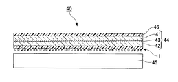
- FIG. 6 is a cross-sectional view showing an example of the liquid crystal display device of the present invention.
- the liquid crystal display device 40 includes a liquid crystal panel 44 having a liquid crystal layer 43 sandwiched between a pair of substrates 41 and 42, a backlight unit 45, and a surface on the side where the fine metal wires are formed.
- the wire grid polarizer 1 of the present invention attached to the surface of the liquid crystal panel 44 on the backlight unit 45 side so that the surface on which the fine line is not formed becomes the viewing side of the liquid crystal display device 40, and the backlight
- An absorption polarizer 46 is attached to the surface of the liquid crystal panel 44 opposite to the unit 45 side.
- liquid crystal display device of the present invention having the wire grid type polarizer of the present invention described above since it has the wire grid type polarizer of the present invention having sufficient scratch resistance and optical properties, sufficient luminance and Has contrast.
- the liquid crystal display device of the present invention having the antireflection article of the present invention has the antireflection article of the present invention having sufficient scratch resistance and antireflection characteristics, so that physical contact during assembly and human Since it is hard to be damaged by contact with a hand or the like and fingerprints are difficult to be attached, it has an excellent characteristic that the antireflection characteristic lasts.
- a wire grid type polarizer was set in a reciprocating wear tester (manufactured by KT Corporation). A wire grid with a load of 50 g, 100 g or 500 g, speed: 140 cm / min, by winding a nell cloth (No. 300) moistened with ethanol around the tip of a cylindrical metal rod having a diameter of 10 mm The surface of the mold polarizer on which the fine metal wires were formed was rubbed 20 times, 50 times, or 200 times.
- the total light transmittance was measured with a haze meter (manufactured by Toyo Seiki Co., Ltd., HAZE-GARDII) under a commercial polarizing plate and crossed Nicols, and the light leakage ⁇ T was determined.
- Abrasion resistance b The antireflective article was set in a reciprocating wear tester (manufactured by KT Corporation). The side on which the protrusion of the antireflection article is formed under the conditions of a load of 500 g and a speed of 140 cm / min by a Nel cloth (No.
- Example 1 A wire grid polarizer 2 as shown in FIG. 2 was manufactured by the following procedure.
- a photocurable resin composition is applied to the surface of a highly transmissive polyethylene terephthalate (PET) film (manufactured by Toyobo Co., Ltd., Cosmo Shine A4300, 100 mm ⁇ 100 mm ⁇ thickness 100 ⁇ m) by spin coating, and photocured to a thickness of about 5 ⁇ m.
- PET polyethylene terephthalate
- a coating film of the conductive resin composition was formed.
- the PET film with a coating film was pressed at 25 ° C. using a rubber roll so that the coating film of the photocurable resin composition was in contact with the mold groove, to a nanoimprint mold having a plurality of grooves formed on the surface. It was.
- the PET film side was irradiated with light of a high-pressure mercury lamp (frequency: 1.5 kHz to 2.0 kHz, main wavelength light: irradiation energy at 255 nm, 315 nm and 365 nm, 365 nm: 1000 mJ) for 15 seconds.
- a high-pressure mercury lamp frequency: 1.5 kHz to 2.0 kHz, main wavelength light: irradiation energy at 255 nm, 315 nm and 365 nm, 365 nm: 1000 mJ
- the nanoimprint mold is slowly separated, and a substrate (Pp) in which a plurality of ridge base portions 12 corresponding to the grooves of the nanoimprint mold are formed on one side of the light-transmitting substrate 10. : 140 nm, Dp: 70 nm, Hp: 160 nm).
- Aluminum was vapor-deposited by the oblique vapor deposition method on the ridge base 12 of the substrate to form a fine metal wire 20 (Hm: 100 nm, Dm: 70 nm).
- Silicon oxide was attached as a target to an in-line type sputtering apparatus (manufactured by Nisshin Seiki Co., Ltd.) equipped with a load lock mechanism.
- the substrate on which the fine metal wires 20 were formed was set in the sputtering apparatus, and silicon oxide was vapor-deposited from the direction perpendicular to the surface on the fine metal wires 20 side to form the inorganic oxide layer 30 made of silicon oxide.
- Each dimension (average value of five locations) obtained from the cross-sectional TEM image was Da: 6.0 nm, Ha: 22.0 nm, and Dat: 58.0 nm.
- the obtained wire grid polarizer 2 was evaluated for scratch resistance a. Moreover, the dynamic friction coefficient was measured about the smooth cured film of the same laminated structure. The results are shown in Table 1.
- Examples 2, 3, 5, 6 Each dimension Pp, Dp, Hp of the substrate produced in the step (I ′) was changed to the values described in Table 1, and the deposition time (sputtering time) in the step (II) was changed.
- a wire grid polarizer 2 was obtained in the same manner as in Example 1 except that the inorganic oxide layer 30 having the dimensions (Ha, Da, Dat) was formed. The obtained wire grid polarizer 2 was evaluated for scratch resistance a. Moreover, the dynamic friction coefficient was measured about the smooth cured film of the same laminated structure. The results are shown in Table 1.
- Example 4 A wire grid polarizer was obtained in the same manner as in Example 3 except that the step (III) was not performed.
- the wire grid polarizer not having the fluorine-containing compound layer 32 was evaluated for scratch resistance I.
- the dynamic friction coefficient was measured about the smooth cured film of the same laminated structure. The results are shown in Table 1.
- Example 7 A wire grid polarizer was obtained in the same manner as in Example 1 except that the steps (II) and (III) were not performed.
- the wire grid type polarizer not having the inorganic oxide layer 30 and the fluorine-containing compound layer 32 was evaluated for scratch resistance a.
- the dynamic friction coefficient was measured about the smooth cured film of the same laminated structure. The results are shown in Table 1.
- Example 8 A wire grid polarizer 2 was obtained in the same manner as in Example 3 except that the dimensions Pp, Dp, and Hp of the substrate produced in the step (I ′) were set to the values shown in Table 1. The obtained wire grid polarizer 2 was evaluated for scratch resistance a. Moreover, the dynamic friction coefficient was measured about the smooth cured film of the same laminated structure. The results are shown in Table 1.
- No. 6 and No. 8 were observed under a high load condition of 500 g ⁇ 200 times, and the observed light leakage ⁇ T was small and excellent in scratch resistance. Further, it was found that the light leakage ⁇ T is rapidly suppressed particularly when the thickness Ha is 40 nm or more.
- a large light leakage ⁇ T was observed in Example 1 with a small thickness Ha, Example 4 without the fluorine-containing compound layer 32, Example 7 without the inorganic oxide layer 30 and the fluorine-containing compound layer 32.
- Example 8 Hp is large compared to the other examples, which is considered to be due to this, but the inorganic oxide layer is not formed so much on the side surface of the ridge (projection), and the thickness (Da) and ratio ( Da / Dat) was small. However, the light leakage ⁇ T was very low and had sufficient scratch resistance. From this, the inorganic oxide layer is coated at least on the top of the ridge (projection), the thickness Ha is 30 nm or more, and the ratio of the thickness Ha to the width Dat (Ha / Dat) is It was understood that if it is 1.0 or less, sufficient scratch resistance is exhibited.
- An antireflection structure 60 as shown in FIG. 7 was manufactured according to the following procedure.
- a photocurable resin composition is applied to the surface of a highly transmissive polyethylene terephthalate (PET) film (manufactured by Toyobo Co., Ltd., Cosmo Shine A4300, 100 mm ⁇ 100 mm ⁇ thickness 100 ⁇ m) by spin coating, and photocured to a thickness of about 5 ⁇ m.
- PET polyethylene terephthalate
- the coating film of the photocurable resin composition is applied to the nanoimprint mold formed on the surface of the PET film with a coating film so that a plurality of grooves (conical shape) and the bottom surface of the cone has a hexagonal close-packed structure.
- a coating film so that a plurality of grooves (conical shape) and the bottom surface of the cone has a hexagonal close-packed structure.
- the PET film side was irradiated with light of a high-pressure mercury lamp (frequency: 1.5 kHz to 2.0 kHz, main wavelength light: irradiation energy at 255 nm, 315 nm and 365 nm, 365 nm: 1000 mJ) for 15 seconds.
- a high-pressure mercury lamp frequency: 1.5 kHz to 2.0 kHz, main wavelength light: irradiation energy at 255 nm, 315 nm and 365 nm, 365 nm: 1000 mJ
- the nanoimprint mold is slowly separated, and a substrate (pitch: a plurality of protrusions 62 corresponding to the grooves of the nanoimprint mold is formed on one surface of the light-transmitting substrate 10. 300 nm, the height of protrusions: 188.9 nm).
- Silicon oxide was attached as a target to an in-line type sputtering apparatus (manufactured by Nisshin Seiki Co., Ltd.) equipped with a load lock mechanism.
- the substrate on which the protrusions 62 were formed was set in the sputtering apparatus, and silicon oxide was vapor-deposited from the direction perpendicular to the surface on the protrusions 62 side to form the inorganic oxide layer 30 made of silicon oxide.
- Each dimension (average value of five locations) obtained from the cross-sectional TEM image was Da: 33.3 nm, Ha: 100.0 nm, and Dat: 200.0 nm.
- a fluorine-containing compound having a hydrolyzable silyl group and a fluoroalkyl group (having an etheric oxygen atom between carbon-carbon atoms) (manufactured by Daikin Industries, Ltd., OPTOOL DSX) and a fluorine-based solvent (manufactured by Asahi Glass Company, CT- Immediately after the substrate on which the protrusions and the inorganic oxide layer were formed was immersed in a solution (concentration: 0.1% by mass) diluted in Solv.100, chemical formula: C 6 F 13 OCH 3 ) and pulled up, immediately fluorinated solvent (manufactured by Asahi Glass Company, CT-Solv.100, chemical formula: C 6 F 13 OCH 3) was rinsed with.
- An antireflective structure 60 was obtained by placing in a constant temperature and humidity chamber at 60 ° C. and 90% RH for 1 hour to form a fluorine-containing compound layer 32 (Df and Hf: 2 nm) on the surface of the inorganic oxide layer 30.
- the obtained antireflection structure 60 was evaluated for scratch resistance b. The results are shown in Table 2.
- Example 10 and 11 An antireflection structure was obtained in the same manner as in Example 9 except that the deposition time (sputtering time) was changed and inorganic oxide layers having the dimensions (Ha, Da, Dat) shown in Table 2 were formed. It was. The antireflection structure thus obtained was evaluated for scratch resistance b. The results are shown in Table 2.
- Example 9 where the thickness Ha of the inorganic oxide layer is 30 nm or more and the ratio of the thickness Ha to the width Dat (Ha / Dat) is 1.0 or less, ⁇ Haze is It was as small as 1 or less and was excellent in scratch resistance. On the other hand, in Example 10 with a small thickness Ha, ⁇ Haze was greater than 1 after 50 scratches. Further, in Example 11 without the fluorine-containing compound layer, ⁇ Haze was greater than 1 after 20 and 50 scratches.
- the microstructured molded body of the present invention can be used as an image display device such as a liquid crystal display device, a rear projection television, and a front projector as a wire grid polarizer, an antireflection article, and the like. Moreover, the microstructure molded body of the present invention can be used as a mold for nanoimprinting. It should be noted that the entire contents of the specification, claims, drawings and abstract of Japanese Patent Application No. 2011-035641 filed on February 22, 2011 are cited here as disclosure of the specification of the present invention. Incorporated.
Abstract
Description
前記無機酸化物層が前記凸部の側面の少なくとも一部を被覆し、該側面に被覆された前記無機酸化物層の幅方向の厚さDaと前記幅Datとの比(Da/Dat)が0.25以下であることが好ましい。
前記含フッ素化合物層は、厚さHfが1~30nmであることが好ましい。
前記含フッ素化合物は、加水分解性シリル基およびフルオロアルキル基(炭素-炭素原子間にエーテル性酸素原子を有していてもよい。)を有することが好ましい。
本発明のワイヤグリッド型偏光子は、本発明の微細構造成形体からなるワイヤグリッド型偏光子であって、前記凸部が、互いに平行に形成された凸条であるとともに、前記凸条の少なくとも頂部は金属層からなり、互いに離間した複数の金属細線が形成されていることを特徴とする。
本発明の反射防止物品は、本発明の微細構造成形体からなることを特徴とする。
本発明の反射防止物品は、本発明の微細構造成形体からなり、前記基板がモスアイ構造を有することが好ましい。
本発明の反射防止物品は、前記基板が、光透過性基板であることが好ましい。
本発明の液晶表示装置は、本発明の微細構造成形体を有すること特徴とする。
たとえば本発明の液晶表示装置は、一対の基板間に液晶層を挟持した液晶パネルと、バックライトユニットと、本発明のワイヤグリッド型偏光子とを有することを特徴とする。
本発明の微細構造成形体としては、ワイヤグリッド型偏光子、反射防止物品などの光学用微細構造成形体が挙げられる。
たとえばワイヤグリッド型偏光子は、凸部として凸条を有し、反射防止物品は凸部として、錐体および該錐体に基く錐台などからなる凸起を有する。
凸部が凸起の場合、ピッチは、最も近接する凸起同士の底面中心間の距離である。
凸起は、各凸起の形状がほぼ一定であることが好ましい。また、断面形状は、角や辺(側面、上面(上底面))が曲線状であってもよい。
〔基板〕
本発明のワイヤグリッド型偏光子の備える基板は、光透過性基板と、該光透過性基板上に互いに平行に配列した複数の金属細線とからなる。該基板としては、平坦な光透過性基板上に、金属細線からなる凸条が形成された基板;凸条の基部(以下、凸条基部と記す。)が形成された光透過性基板の該凸条基部上に、凸条の上部(以下、凸条上部と記す。)を構成する金属細線が形成された基板が挙げられる。ワイヤグリッド型偏光子の凸条の少なくとも頂部は金属層からなり、それにより、互いに離間した複数の金属細線が形成されている。
光透過性基板は、ワイヤグリッド型偏光子の使用波長範囲において光透過性を有する。光透過性とは、光を透過することを意味し、使用波長範囲は、具体的には、400nm~800nmの範囲である。
金属細線としては、平坦な光透過性基板の表面に形成された金属または金属化合物からなる金属層をパターニングして形成されたものが挙げられる。この場合、パターニングにより形成された金属細線が基板の凸条となる。金属細線としては、複数の凸条基部が、該凸条基部間に形成される平坦部を介して互いに平行にかつ所定のピッチで表面に形成された光透過性基板の該凸条基部の表面に、選択的に金属または金属化合物からなる金属層を形成したものも挙げられる。この場合、金属細線からなる凸条上部と、光透過性基板の有する凸条基部とで、基板の凸条が構成される。
金属細線の材料としては、可視光に対する反射率が高く、可視光の吸収が少なく、かつ高い導電率を有する点から、アルミニウム、アルミニウム系合金、銀、クロム、またはマグネシウムが好ましく、アルミニウム、またはアルミニウム系合金が特に好ましい。
無機酸化物層は、少なくとも基板の凸条の頂部を被覆する層である。無機酸化物層は、凸条の2つの側面の少なくとも一部や、凸条間の基板の表面(凸条間の平坦部)を被覆していてもよいが、凸条の頂部のみを被覆していても、充分な効果(耐擦傷性および光学特性)が得られる。
また、凸条の頂部を被覆する無機酸化物層の厚さHaと、凸条の頂部を被覆する無機酸化物層の幅Datとの比(Ha/Dat)が1.0以下である。比(Ha/Dat)は、0.4~0.8であるのが好ましい。比(Ha/Dat)が1.0以下であると、凸条の頂部を被覆する無機酸化物層は折損せず、凸条の耐擦傷性を高める。ここでDatは、凸条の頂部よりも上に存在し、該頂部を被覆する無機酸化物層の幅であり、該幅が無機酸化物層の高さ方向において異なる場合には、その最大幅である。
含フッ素化合物層は、無機酸化物層の表面を、無機酸化物に対して反応性を有する基を有する含フッ素化合物で処理して形成された層であり、無機酸化物層の全面を被覆する。たとえば、含フッ素化合物が後述する加水分解性シリル基およびフルオロアルキル基を有する含フッ素化合物の場合、含フッ素化合物層は、該含フッ素化合物の加水分解縮合体から構成される。
含フッ素化合物層の動摩擦係数は、ASTM D 1894に準拠して測定する。
本発明のワイヤグリッド型偏光子の製造方法としては、金属細線の形成方法の違いによって下記の方法(α)、方法(β)が挙げられる。
(I)平坦な光透過性基板の表面に金属層を形成し、該金属層をパターニングして、互いに平行にかつ所定のピッチで配列した複数の金属細線を形成し、基板を作製する工程。
(II)金属細線が形成された側の基板上に、無機酸化物を蒸着して無機酸化物層を形成する工程。
(III)無機酸化物層の表面を、無機酸化物に対して反応性を有する基を有する含フッ素化合物で処理して含フッ素化合物層を形成する工程。
該方法(α)の場合、工程(I)で形成された金属細線が基板の凸条となる。
(I’)表面に複数の凸条基部が互いに平行にかつ所定のピッチで形成された光透過性基板を作製し、凸条基部の表面に選択的に金属または金属化合物を蒸着して、互いに平行に配列した複数の金属細線を形成し、基板を作製する工程。
(II)金属細線が形成された側の基板上に、無機酸化物を蒸着して無機酸化物層を形成する工程。
(III)無機酸化物層の表面を、無機酸化物に対して反応性を有する基を有する含フッ素化合物で処理して含フッ素化合物層を形成する工程。
該方法(β)の場合、光透過性基板の凸条基部と金属細線(凸条上部)とで、基板の凸条が構成される。
(工程(I))
金属細線は、平坦な光透過性基板の表面に金属層を形成し、該金属層をパターニングすることによって形成される。
無機酸化物層は、金属細線が形成された側の基板上に、無機酸化物を蒸着して形成される。
含フッ素化合物層は、無機酸化物層の表面を、無機酸化物に対して反応性を有する基を有する含フッ素化合物で処理して形成される。
(i)金属細線および無機酸化物層が形成された基板を、含フッ素化合物の希釈溶液に浸漬する工程。
(ii)前記基板を含フッ素化合物の希釈溶液から引き上げた後、基板を溶媒でリンスする工程。
(iii)前記基板をリンスした後、恒温恒湿条件下に置き、加水分解性シリル基を加水分解、縮合させ、含フッ素化合物層を形成する工程。
含フッ素化合物層と無機酸化物層との縮合度は、例えば工程(i)で用いる希釈溶液の濃度、恒温恒湿条件および時間を調整することにより、制御できる。
(工程(I’))
光透過性基板の作製方法としては、インプリント法(光インプリント法、熱インプリント法)、リソグラフィ法等が挙げられ、凸条基部を生産性よく形成できる点および光透過性基板を大面積化できる点から、インプリント法が好ましく、凸条基部をより生産性よく形成できる点およびモールドの溝を精度よく転写できる点から、光インプリント法が特に好ましい。
(i)光硬化性組成物を基材の表面に塗布する工程。
(ii)複数の溝が互いに平行にかつ所定のピッチで形成されたモールドを、溝が光硬化性組成物に接するように、光硬化性組成物に押しつける工程。
(iii)モールドを光硬化性組成物に押しつけた状態で放射線(紫外線、電子線等)を照射して光硬化性組成物を硬化させて、モールドの溝に対応する複数の凸条基部を有する光透過性基板を作製する工程。
(iv)光透過性基板からモールドを分離する工程。
なお、凸条基部を有する表層と基材とが一体化したものを光透過性基板として用いてもよく、凸条基部を有する表層を基材から分離したものを光透過性基板として用いてもよい。また、金属層を形成した後に、凸条基部を有する表層を基材から分離してもよい。
(i)基材の表面に熱可塑性樹脂の被転写膜を形成する工程、または熱可塑性樹脂の被転写フィルムを作製する工程。
(ii)複数の溝が互いに平行にかつ一定のピッチで形成されたモールドを、溝が被転写膜または被転写フィルムに接するように、熱可塑性樹脂のガラス転移温度(Tg)または融点(Tm)以上に加熱した被転写膜または被転写フィルムに押しつけ、モールドの溝に対応する複数の凸条基部を有する光透過性基板を作製する工程。
(iii)光透過性基板本体をTgまたはTmより低い温度に冷却して光透過性基板からモールドを分離する工程。
なお、凸条基部を有する表層と基材とが一体化したものを光透過性基板として用いてもよく、凸条基部を有する表層を基材から分離したものを光透過性基板として用いてもよい。また、金属層を形成した後に、凸条基部を有する表層を基材から分離してもよい。
工程(II)~(III)は、方法(α)における工程(II)~(III)と同様に行えばよい。
以下、本発明のワイヤグリッド型偏光子の実施形態を、図を用いて説明する。以下の図は模式図であり、実際のワイヤグリッド型偏光子は、図示したような理論的かつ理想的形状を有するものではない。たとえば、実際のワイヤグリッド型偏光子においては、金属細線、凸条等の形状の崩れが多少ある。
なお、本発明における各寸法は、ワイヤグリッド型偏光子の断面の透過型電子顕微鏡(TEM)像において、任意の5箇所について各寸法を測定し、平均した値とする。
図1は、本発明のワイヤグリッド型偏光子の第1の実施形態を示す断面図である。ワイヤグリッド型偏光子1は、平坦な光透過性基板10と、該光透過性基板10の表面に互いに平行にかつ可視光の波長以下の所定のピッチPpで形成された断面形状が矩形である複数の金属細線20からなる凸条50とを有する基板と;凸条50の2つの側面およびこれらに挟まれた頂部52と、凸条50間の基板の平坦部13とを、凸条50間の溝14に空隙が形成されるように被覆する無機酸化物層30と;無機酸化物層30の全面を、無機酸化物に対して反応性を有する基を有する含フッ素化合物で処理して形成された含フッ素化合物層32とを有する。
なお、以下に説明する第1~第3の実施形態では、無機酸化物層30は、凸条50の2つの側面およびこれらに挟まれた頂部52と、凸条50間の基板の平坦部13とを被覆した例を示しているが、無機酸化物層は凸条の頂部のみを被覆していてもよく、その場合でも、優れた耐擦傷性および光学特性は充分に発揮される。
Dmは、金属細線20を形成しやすい点から、10~100nmが好ましい。
凸条50の側面を被覆する無機酸化物層30の厚さDa(凸条50の幅方向)と前述の幅Datとの比(Da/Dat)は、前述のとおり0.25以下であることが好ましい。
Daは、前述のとおり、凸条の全高さをH’(=Hm)とした場合、その半分の高さ(H’/2)の位置において、側面に被覆されている無機酸化物層の幅方向の厚さである。なお、図示例では、Daは高さ方向に一定であるが、一定でなくてもよい。
ワイヤグリッド型偏光子1は、上述した方法(α)によって製造できる。
(ワイヤグリッド型偏光子)
図2は、本発明のワイヤグリッド型偏光子の第2の実施形態を示す断面図である。ワイヤグリッド型偏光子2は、断面形状が矩形である複数の凸条50が、該凸条50間に形成される溝14の平坦部13を介して互いに平行にかつ可視光の波長以下の所定のピッチPpで光透過性基板10の表面に形成された基板と;凸条50の2つの側面およびこれらに挟まれた頂部52と、凸条50間の基板の平坦部13とを、凸条50間の溝14に空隙が形成されるように被覆する無機酸化物層30と;無機酸化物層30の全面を、無機酸化物に対して反応性を有する基を有する含フッ素化合物で処理して形成された含フッ素化合物層32とを有する。
Dpは、蒸着によって金属層を形成しやすい点から、10~100nmが好ましい。
凸条50の側面を被覆する無機酸化物層30の厚さDa(凸条50の幅方向)と前述の幅Datとの比(Da/Dat)は、前述のとおり0.25以下であることが好ましい。
この例では、凸条の全高さH’=Hm+Hpであり、Daは、その半分の高さ(H’/2)の位置において、側面に被覆されている無機酸化物層の幅方向の厚さである。なお、図示例では、Daは高さ方向に一定であるが、一定でなくてもよい。
ワイヤグリッド型偏光子2は、上述した方法(β)によって製造できる。
蒸着量が15~100nmとなる条件とは、凸条基部に被覆層を形成する際に、凸条基部が形成されていない平坦な部分の表面に金属または金属化合物を蒸着して形成される金属層の厚さtが15~100nmとなるような条件である。
凸条基部12の長さ方向Lに対して略直交し、かつ凸条基部12の高さ方向Hに対して第2の側面18の側に角度θLをなす方向V2の延長線上に蒸着源が位置するように、蒸着源に対向して配置された光透過性基板10の傾きを変更できる蒸着装置。
(ワイヤグリッド型偏光子)
図4は、本発明のワイヤグリッド型偏光子の第3の実施形態を示す斜視図である。ワイヤグリッド型偏光子3は、複数の凸条50が、該凸条50間に形成される溝14の平坦部13を介して互いに平行にかつ可視光の波長以下の所定のピッチPpで光透過性基板10の表面に形成された基板と;凸条50の側面および頂部52と、凸条50間の基板の平坦部13とを、凸条50間の溝14に空隙が形成されるように被覆する無機酸化物層30と;無機酸化物層30の全面を、無機酸化物に対して反応性を有する基を有する含フッ素化合物で処理して形成された含フッ素化合物層32とを有する。
凸条50の側面を被覆する無機酸化物層30の厚さDa(凸条50の幅方向)と前述の幅Datとの比(Da/Dat)は、前述のとおり0.25以下であることが好ましい。
この例では、凸条の全高さH’=Hm1+Hpであり、Daは、その半分の高さ(H’/2)の位置において、側面に被覆されている無機酸化物層の幅方向の厚さである。なお、図示例では、Daは高さ方向に一定であるが、一定でなくてもよい。
光透過性基板10の厚さHsは、0.5~1000μmが好ましく、1~200μmがより好ましい。
ワイヤグリッド型偏光子3は、上述した方法(β)によって製造できる。
tan(θR1±10)=(Pp-Dpb/2)/Hp ・・・(a)。
角度θR1(°)は、tan(θR1±7)=(Pp-Dpb/2)/Hpを満たすことが好ましく、tan(θR1±5)=(Pp-Dpb/2)/Hpを満たすことがより好ましい。
蒸着量が4~25nmとなる条件とは、凸条基部に被覆層を形成する際に、凸条基部が形成されていない平坦な部分の表面に金属または金属化合物を蒸着して形成される金属層の厚さtが4~25nmとなるような条件である。
θR1+3≦θR2≦θR1+30 ・・・(b)。
角度θR2(°)は、θR1+6≦θR2≦θR1+25を満たすことが好ましく、θR1+10≦θR2≦θR1+20を満たすことがより好ましい。
本発明のワイヤグリッド型偏光子は、凸条の頂部に被覆された無機酸化物層の厚さHaが30nm以上で、かつ、該厚さHaと幅Datとの比(Ha/Dat)が1.0以下である限り、図示例のものに限定されない。
たとえば、光透過性基板と金属細線との間に、第2の無機酸化物層(酸化アルミニウム等)を有するものであってもよい。
また、無機酸化物層は、同種または異種の複数の無機酸化物層からなる積層構造を有していてもよい。
〔基板〕
本発明の反射防止物品の備える基板は、光透過性基板からなることが好ましい。基板の少なくとも一方の面には、円錐、角錐などの錐体および該錐体に基く錐台などからなり、可視光の波長以下の所定のピッチで形成された凸起(凸部)が形成されており、基板は、いわゆるモスアイ構造を有している。
ピッチは、400nmを超えると短波長域の反射率が上昇することがあることから、400nm以下が好ましく、300nm以下がより好ましい。
凸起の形状は、円錐が好ましい。また、凸起の高さは、凸起が折れ曲がりにくくなる点、生産性に優れる点から、凸起の高さを底辺で割った値であるアスペクト比が、2以下であることが好ましい。凸起一つ当たりのアスペクト比又は高さが低すぎる場合、短波長側(青)の光を反射することがあるため、アスペクト比は0.8以上が好ましい。
また、光透過性基板は、積層体であってもよく、たとえば、熱可塑性樹脂、ガラス等からなる基材と、該基材の表面に形成された光硬化樹脂からなる凸起を有する表層とを備えるものが挙げられる。
無機酸化物層は、光透過性基板の少なくとも凸起の頂部を被覆する層である。無機酸化物層は、凸起の側面の少なくとも一部や、凸起間の基板の表面(凸起間の平坦部)を被覆していてもよいが、凸起の頂部のみを被覆していても、充分な効果(耐擦傷性および光学特性)が得られる。無機酸化物層は、光透過性基板層を直接被覆していることが好ましい。無機酸化物層の材料としては、ワイヤグリッド型偏光子において例示した材料を同様に使用できる。すなわち、酸化ケイ素、酸化ジルコニウム、酸化スズ、酸化チタン、酸化アルミニウム等が挙げられ、反射防止物品が可視光領域で高い透過率を示す点から、酸化ケイ素、酸化ジルコニウム、酸化スズが好ましく、コストの点から、酸化ケイ素が特に好ましい。
また、凸起の頂部を被覆する無機酸化物層の厚さHaと、凸起の頂部を被覆する無機酸化物層の幅Datとの比(Ha/Dat)が1.0以下である。比(Ha/Dat)が1.0以下であると、凸起の頂部を被覆する無機酸化物層は折損し難く、凸起の耐擦傷性を高める。ここで幅Datとしては、凸起の頂部よりも上に存在し、該頂部を被覆する無機酸化物層の径(基板の主表面と平行方向)の値を採用する。該径が無機酸化物の高さ方向で一定でない場合および該径が周方向で一定でない場合の少なくとも一方を満たす場合には、Datとしては径の最大値を採用する。
また、各寸法については、ワイヤグリッド偏光子についての先の記載にあるように、透過型電子顕微鏡(TEM)像において、任意の5箇所について測定し、平均した値を採用する。
反射防止物品の断面の透過型電子顕微鏡(TEM)像から、凸起の頂部を通っている縦断面像を複数選択する。その縦断面像が、凸起の頂部を通っているものかどうかは、その縦断面像における凸起の高さから判断できる。そして、これら選択された縦断面像における(H’/2)の位置の任意の5箇所について、無機酸化物層の厚さを測定し、その平均値を求める。
含フッ素化合物層は、無機酸化物層の表面を、無機酸化物に対して反応性を有する基を有する含フッ素化合物で処理して形成された層であり、無機酸化物層の全面を被覆する。無機酸化物に対して反応性を有する基および好ましい基ならびに含フッ素化合物、含フッ素化合物層の厚み等は、ワイヤグリッド型偏光子において例示したとおりである。たとえば、含フッ素化合物が後述する加水分解性シリル基およびフルオロアルキル基を有する含フッ素化合物の場合、含フッ素化合物層は、該含フッ素化合物の加水分解縮合体から構成される。
また、ASTM D 1894に準拠して測定された含フッ素化合物層の動摩擦係数は、耐擦傷性の点から、0.2以下が好ましく、0.15以下がより好ましい。
凸起62の側面を被覆する無機酸化物層30の厚さDa(凸起62の幅方向)と前述の幅Datとの比(Da/Dat)は、前述のとおり0.25以下であることが好ましい。
Daは、前述のとおり、凸起62の高さHpの半分の高さ(Hp/2)の位置において、側面に被覆されている無機酸化物層の幅方向の厚さである。
光透過性基板の作製方法としては、インプリント法(光インプリント法、熱インプリント法)、リソグラフィ法等が挙げられ、凸起を生産性よく形成できる点および光透過性基板を大面積化できる点から、インプリント法が好ましく、凸起をより生産性よく形成できる点およびモールドの溝を精度よく転写できる点から、光インプリント法が特に好ましい。インプリント法に用いられるモールド、基材等は、ワイヤグリッド型偏光子において例示したものを同様に使用できる。
無機酸化物層および含フッ素化合物層の形成は、ワイヤグリッド型偏光子を製造する方法(α)における工程(II)~(III)と同様に行えばよい。
本発明のワイヤグリッド型偏光子、反射防止物品などの微細構造成形体にあっては、少なくとも凸部の頂部を被覆する無機酸化物層を有し、凸部の頂部に被覆された無機酸化物層は、厚さHaが30nm以上で、かつ、該厚さHaと幅Datとの比(Ha/Dat)が1.0以下である。また、少なくとも無機酸化物層の表面には、無機酸化物に対して反応性を有する基を有する含フッ素化合物で処理して形成され、表面の動摩擦係数を低く抑える含フッ素化合物層が形成されている。そのため、本発明の微細構造成形体は、優れた耐擦傷性を有する。
本発明の液晶表示装置は、本発明の微細構造成形体を有する。
本発明の液晶表示装置は、たとえば、一対の基板間に液晶層を挟持した液晶パネルと、バックライトユニットと、本発明のワイヤグリッド型偏光子とを有する。また、本発明の液晶表示装置は、たとえば、液晶パネルの表面に、本発明の反射防止物品を有する。
また、本発明の反射防止物品を有する本発明の液晶表示装置にあっては、充分な耐擦傷性および反射防止特性を有する本発明の反射防止物品を有するため、アッセンブリ時の物理的接触や人間の手などの接触に対して傷付きにくく、指紋も付きにくいため反射防止特性が持続する優れた特性を有する。
例2、3、5、6、8、9は実施例であり、例1、4、7、10、11は比較例である。
ワイヤグリッド型偏光子を往復式摩耗試験機(ケイエヌテー社製)にセットした。直径10mmの円柱状の金属製棒の先端にエタノールで湿らせたネル布(300番)を巻きつけたものによって、荷重:50g、100gまたは500g、速度:140cm/minの条件にて、ワイヤグリッド型偏光子の金属細線が形成された側の表面を、20回、50回または200回擦った。試験後のワイヤグリッド型偏光子について、市販偏光板とクロスニコル下、ヘーズメーター(東洋精機社製、HAZE-GARDII)にて全光線透過率を測定し、光漏れΔTを求めた。
(耐擦傷性b)
反射防止物品を往復式摩耗試験機(ケイエヌテー社製)にセットした。直径10mmの円柱状の金属製棒の先端にネル布(300番)を巻きつけたものによって、荷重:500g、速度:140cm/minの条件にて、反射防止物品の凸起が形成された側の表面を、20回または50回擦った。試験前後の反射防止物品について、ヘーズメーター(東洋精機社製、HAZE-GARDII)にてヘーズ値を測定し、その差(ΔHaze)を得た。
ワイヤグリッド型偏光子と同一の積層構造を有し、かつ微細構造を持たない平滑な硬化膜を表面性試験機(新東科学工業社製、HEIDON-14S)にセットした。平面圧子を用い、垂直荷重:200g、すべり速度:100mm/minの条件にて、平滑表面について摩擦抵抗試験を行い、ASTM D 1894に準拠して動摩擦係数を求めた。
撹拌機および冷却管を装着した300mLの4つ口フラスコに、
単量体1(新中村化学工業社製、NK エステル A-DPH、ジペンタエリスリトールヘキサアクリレート)の60g、
単量体2(新中村化学工業社製、NK エステル A-NPG、ネオペンチルグリコールジアクリレート)の40g、
光重合開始剤1(チバスペシャリティーケミカルズ社製、IRGACURE907)の4.0g、
を入れた。フラスコ内を常温および遮光にした状態で、1時間撹拌して均一化し、粘度が140mPa・sである光硬化性樹脂組成物を得た。
図2に示すようなワイヤグリッド型偏光子2を、下記の手順にて製造した。
高透過ポリエチレンテレフタレート(PET)フィルム(東洋紡社製、コスモシャインA4300、100mm×100mm×厚さ100μm)の表面に、光硬化性樹脂組成物をスピンコート法により塗布し、厚さ約5μmの光硬化性樹脂組成物の塗膜を形成した。
ロードロック機構を備えたインライン型スパッタ装置(日真精機社製)に、ターゲットとして酸化ケイ素を取り付けた。スパッタ装置内に、金属細線20が形成された基板をセットし、金属細線20側の表面に対して垂直方向から酸化ケイ素を蒸着させ、酸化ケイ素からなる無機酸化物層30を形成した。
断面のTEM像から求めた各寸法(5箇所の平均値)は、Da:6.0nm、Ha:22.0nm、Dat:58.0nmであった。
加水分解性シリル基およびフルオロアルキル基(炭素-炭素原子間にエーテル性酸素原子を有する。)を有する含フッ素化合物(ダイキン工業社製、オプツールDSX)を、フッ素系溶媒(旭硝子社製、CT-Solv.100、化学式:C6F13OCH3)に希釈させた溶液(濃度:0.1質量%)に、金属細線20および無機酸化物層30が形成された基板を浸漬し、引き上げた後、直ちにフッ素系溶媒(旭硝子社製、CT-Solv.100、化学式:C6F13OCH3)でリンスした。60℃、90%RHの恒温恒湿槽中に1時間置き、無機酸化物層30の表面に含フッ素化合物層32(DfおよびHf:2nm)を形成し、ワイヤグリッド型偏光子2を得た。
工程(I’)で作製する基板の各寸法Pp、Dp、Hpを表1に記載の値とした点、工程(II)における蒸着時間(スパッタ処理時間)を変更し、表1に記載の各寸法(Ha、Da、Dat)を有する無機酸化物層30を形成した点以外は、例1と同様にしてワイヤグリッド型偏光子2を得た。
得られたワイヤグリッド型偏光子2について、耐擦傷性aの評価を行った。また、同一積層構造の平滑硬化膜について動摩擦係数の測定を行った。結果を表1に示す。
工程(III)を行なわない以外は、例3と同様にしてワイヤグリッド型偏光子を得た。
含フッ素化合物層32を有さないワイヤグリッド型偏光子について、耐擦傷性Iの評価を行った。また、同一積層構造の平滑硬化膜について動摩擦係数の測定を行った。結果を表1に示す。
工程(II)および工程(III)を行なわない以外は、例1と同様にしてワイヤグリッド型偏光子を得た。
無機酸化物層30および含フッ素化合物層32を有さないワイヤグリッド型偏光子について、耐擦傷性aの評価を行った。また、同一積層構造の平滑硬化膜について動摩擦係数の測定を行った。結果を表1に示す。
工程(I’)で作製する基板の各寸法Pp、Dp、Hpを表1に記載の値とした以外は、例3と同様にしてワイヤグリッド型偏光子2を得た。
得られたワイヤグリッド型偏光子2について、耐擦傷性aの評価を行った。また、同一積層構造の平滑硬化膜について動摩擦係数の測定を行った。結果を表1に示す。
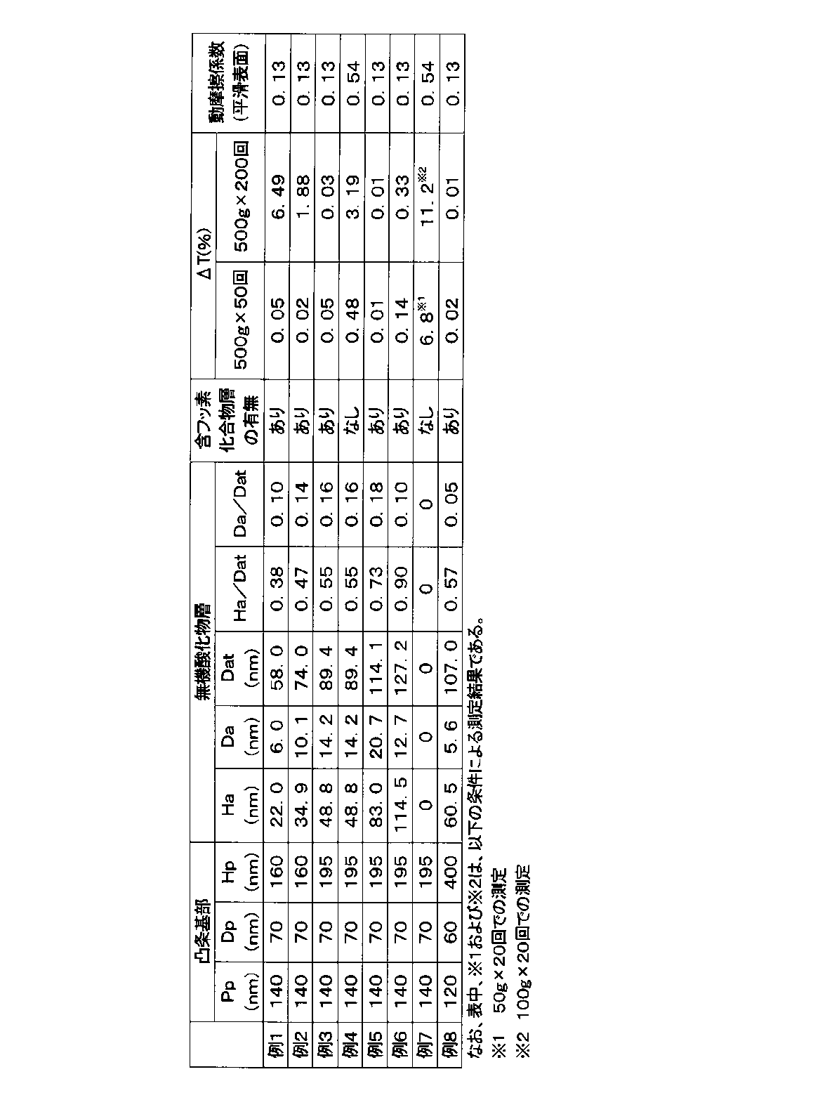
これに対して、厚さHaが小さい例1、含フッ素化合物層32のない例4、無機酸化物層30および含フッ素化合物層32のない例7では、大きな光漏れΔTが観察された。
また、特に例8は、Hpが他の例に比べて大きく、そのためと考えられるが、無機酸化物層が凸条(凸部)の側面にはあまり形成されず、厚み(Da)および比(Da/Dat)が小さかった。しかしながら、光漏れΔTは非常に低く、充分な耐擦傷性を備えていた。このことから、無機酸化物層が少なくとも凸条(凸部)の頂部に被覆されていて、厚さHaが30nm以上で、かつ、該厚さHaと幅Datとの比(Ha/Dat)が1.0以下であれば、充分な耐擦傷性が発揮されることが理解された。
図7に示すような反射防止構造体60を、下記の手順にて製造した。
高透過ポリエチレンテレフタレート(PET)フィルム(東洋紡社製、コスモシャインA4300、100mm×100mm×厚さ100μm)の表面に、光硬化性樹脂組成物をスピンコート法により塗布し、厚さ約5μmの光硬化性樹脂組成物の塗膜を形成した。
断面のTEM像から求めた各寸法(5箇所の平均値)は、Da:33.3nm、Ha:100.0nm、Dat:200.0nmであった。
蒸着時間(スパッタ処理時間)を変更し、表2に記載の各寸法(Ha、Da、Dat)を有する無機酸化物層を形成した点以外は、例9と同様にして反射防止構造体を得た。
得られた反射防止構造体について、耐擦傷性bの評価を行った。結果を表2に示す。
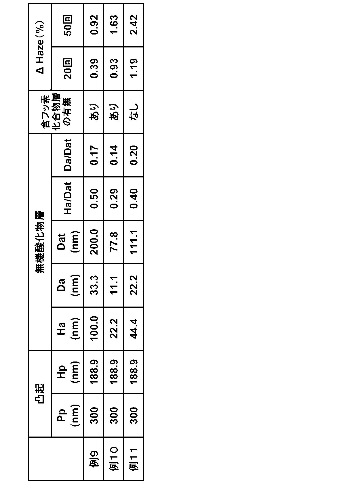
これに対して、厚さHaが小さい例10では、擦傷回数50回で、ΔHazeが1より大きくなった。また、含フッ素化合物層のない例11では、擦傷回数20回および50回で、ΔHazeが1より大きくなった。
なお、2011年2月22日に出願された日本特許出願2011-035641号の明細書、特許請求の範囲、図面及び要約書の全内容をここに引用し、本発明の明細書の開示として、取り入れるものである。
2 ワイヤグリッド型偏光子
3 ワイヤグリッド型偏光子
10 光透過性基板
20 金属細線
30 無機酸化物層
32 含フッ素化合物層
40 液晶表示装置
44 液晶パネル
45 バックライトユニット
50 凸条
60 反射防止物品
62 凸起
Claims (10)
- 少なくとも一方の面に、可視光の波長以下のピッチで凸部が形成された基板と、
前記凸部の少なくとも頂部を被覆する無機酸化物層と、
少なくとも前記無機酸化物層の表面を、無機酸化物に対して反応性を有する基を有する含フッ素化合物で処理して形成された含フッ素化合物層とを有し、
前記凸部の頂部に被覆された前記無機酸化物層は、厚さHaが30nm以上で、かつ、該厚さHaと幅Datとの比(Ha/Dat)が1.0以下である、微細構造成形体。 - 前記無機酸化物層が前記凸部の側面の少なくとも一部を被覆し、該側面に被覆された前記無機酸化物層の幅方向の厚さDaと前記幅Datとの比(Da/Dat)が0.25以下である、請求項1に記載の微細構造成形体。
- 前記含フッ素化合物層は、厚さHfが1~30nmである、請求項1または2に記載の微細構造成形体。
- 前記含フッ素化合物は、加水分解性シリル基およびフルオロアルキル基(炭素-炭素原子間にエーテル性酸素原子を有していてもよい。)を有する、請求項1~3のいずれか1項に記載の微細構造成形体。
- 請求項1~4のいずれか1項に記載の微細構造成形体からなるワイヤグリッド型偏光子であって、前記凸部が、互いに平行に形成された凸条であるとともに、前記凸条の少なくとも頂部は金属層からなり、互いに離間した複数の金属細線が形成されている、ワイヤグリッド型偏光子。
- 請求項1~4のいずれか1項に記載の微細構造成形体からなる、反射防止物品。
- 請求項1~4のいずれか1項に記載の微細構造成形体からなる反射防止物品であって、
前記基板がモスアイ構造を有する、反射防止物品。 - 前記基板が、光透過性基板である、請求項7に記載の反射防止物品。
- 請求項1~4のいずれか1項に記載の微細構造成形体を有する、液晶表示装置。
- 一対の基板間に液晶層を挟持した液晶パネルと、
バックライトユニットと、
請求項5に記載のワイヤグリッド型偏光子と
を有する、液晶表示装置。
Priority Applications (5)
| Application Number | Priority Date | Filing Date | Title |
|---|---|---|---|
| JP2013501035A JPWO2012115059A1 (ja) | 2011-02-22 | 2012-02-20 | 微細構造成形体および該微細構造成形体を備えた液晶表示装置 |
| CN201280009982XA CN103392135A (zh) | 2011-02-22 | 2012-02-20 | 微细结构成形体和包括该微细结构成形体的液晶显示装置 |
| KR1020137019607A KR20140006840A (ko) | 2011-02-22 | 2012-02-20 | 미세 구조 성형체 및 그 미세 구조 성형체를 구비한 액정 표시 장치 |
| EP12750015.5A EP2680048A4 (en) | 2011-02-22 | 2012-02-20 | FINE STRUCTURE SHAPE AND LIQUID CRYSTAL DISPLAY DEVICE COMPRISING A FINE STRUCTURE FORM |
| US13/973,374 US20130342794A1 (en) | 2011-02-22 | 2013-08-22 | Fine structure form and liquid crystal display device comprising the fine structure form |
Applications Claiming Priority (2)
| Application Number | Priority Date | Filing Date | Title |
|---|---|---|---|
| JP2011-035641 | 2011-02-22 | ||
| JP2011035641 | 2011-02-22 |
Related Child Applications (1)
| Application Number | Title | Priority Date | Filing Date |
|---|---|---|---|
| US13/973,374 Continuation US20130342794A1 (en) | 2011-02-22 | 2013-08-22 | Fine structure form and liquid crystal display device comprising the fine structure form |
Publications (1)
| Publication Number | Publication Date |
|---|---|
| WO2012115059A1 true WO2012115059A1 (ja) | 2012-08-30 |
Family
ID=46720836
Family Applications (1)
| Application Number | Title | Priority Date | Filing Date |
|---|---|---|---|
| PCT/JP2012/054018 WO2012115059A1 (ja) | 2011-02-22 | 2012-02-20 | 微細構造成形体および該微細構造成形体を備えた液晶表示装置 |
Country Status (7)
| Country | Link |
|---|---|
| US (1) | US20130342794A1 (ja) |
| EP (1) | EP2680048A4 (ja) |
| JP (1) | JPWO2012115059A1 (ja) |
| KR (1) | KR20140006840A (ja) |
| CN (1) | CN103392135A (ja) |
| TW (1) | TW201243381A (ja) |
| WO (1) | WO2012115059A1 (ja) |
Cited By (10)
| Publication number | Priority date | Publication date | Assignee | Title |
|---|---|---|---|---|
| JP2014085516A (ja) * | 2012-10-24 | 2014-05-12 | Asahi Kasei E-Materials Corp | ワイヤグリッド偏光板及びその製造方法 |
| WO2015014073A1 (zh) * | 2013-07-30 | 2015-02-05 | 合肥京东方光电科技有限公司 | 显示基板及其制造方法、显示装置 |
| WO2015194649A1 (ja) * | 2014-06-19 | 2015-12-23 | デクセリアルズ株式会社 | 光学体、フィルム貼付体、及び光学体の製造方法 |
| JP2018025748A (ja) * | 2016-05-12 | 2018-02-15 | Jxtgエネルギー株式会社 | 光学位相差部材及びプロジェクタ |
| JP2018511816A (ja) * | 2015-04-03 | 2018-04-26 | モックステック・インコーポレーテッド | ワイヤグリッドポラライザ用の酸化バリア層および吸湿バリア層 |
| JP2018163253A (ja) * | 2017-03-24 | 2018-10-18 | 大日本印刷株式会社 | 偏光子 |
| JP2019144335A (ja) * | 2018-02-19 | 2019-08-29 | デクセリアルズ株式会社 | 微細構造体及びその製造方法、並びに光学機器 |
| WO2020071257A1 (ja) * | 2018-10-01 | 2020-04-09 | Agc株式会社 | ワイヤグリッド型偏光子、偏光板、映像表示装置 |
| WO2021241439A1 (ja) * | 2020-05-25 | 2021-12-02 | デクセリアルズ株式会社 | 偏光板及びその製造方法、ならびに光学機器 |
| JP2022510085A (ja) * | 2018-10-03 | 2022-01-26 | モックステック・インコーポレーテッド | 耐久性のある高性能ワイヤグリッド偏光子 |
Families Citing this family (19)
| Publication number | Priority date | Publication date | Assignee | Title |
|---|---|---|---|---|
| US9632223B2 (en) * | 2013-10-24 | 2017-04-25 | Moxtek, Inc. | Wire grid polarizer with side region |
| KR20160031612A (ko) * | 2014-09-12 | 2016-03-23 | 삼성디스플레이 주식회사 | 와이어 그리드 편광자, 이를 포함하는 표시 장치 및 이의 제조방법 |
| KR20160060860A (ko) * | 2014-11-20 | 2016-05-31 | 삼성디스플레이 주식회사 | 와이어 그리드 편광자, 이를 포함하는 표시 장치 및 이의 제조방법 |
| KR102422109B1 (ko) | 2015-01-08 | 2022-07-19 | 삼성디스플레이 주식회사 | 액정 표시 장치 및 이를 제조하는 방법 |
| US10234613B2 (en) | 2015-02-06 | 2019-03-19 | Moxtek, Inc. | High contrast inverse polarizer |
| US20160231487A1 (en) * | 2015-02-06 | 2016-08-11 | Moxtek, Inc. | High Contrast Inverse Polarizer |
| US10534120B2 (en) | 2015-04-03 | 2020-01-14 | Moxtek, Inc. | Wire grid polarizer with protected wires |
| JP5951165B1 (ja) * | 2015-04-30 | 2016-07-13 | シャープ株式会社 | 光学フィルムの製造方法、及び、光学フィルム |
| JP6377285B2 (ja) * | 2015-10-28 | 2018-08-22 | デクセリアルズ株式会社 | 偏光素子およびその製造方法 |
| KR20170062590A (ko) * | 2015-11-27 | 2017-06-08 | 삼성디스플레이 주식회사 | 와이어 그리드 편광판 및 이의 제조방법 |
| KR20170079671A (ko) * | 2015-12-30 | 2017-07-10 | 코오롱인더스트리 주식회사 | 와이어 그리드 편광판 및 이를 포함한 액정표시장치 |
| KR102567008B1 (ko) * | 2016-03-18 | 2023-08-14 | 삼성디스플레이 주식회사 | 금속선 편광자를 포함하는 표시 장치 및 그 제조 방법 |
| CN105700058A (zh) * | 2016-04-05 | 2016-06-22 | 武汉华星光电技术有限公司 | 显示背光用金属线栅增亮膜及其制备方法 |
| US10797633B2 (en) * | 2016-11-10 | 2020-10-06 | Mitsubishi Electric Research Laboratories, Inc. | Thermal emitter for energy conversion technical field |
| JP6922279B2 (ja) * | 2017-03-14 | 2021-08-18 | セイコーエプソン株式会社 | ワイヤーグリッド偏光素子および投射型表示装置 |
| JP2019061125A (ja) * | 2017-09-27 | 2019-04-18 | デクセリアルズ株式会社 | 偏光板及びその製造方法、並びに光学機器 |
| KR102391028B1 (ko) * | 2019-01-25 | 2022-04-25 | 삼성에스디아이 주식회사 | 편광판 및 이를 포함하는 광학표시장치 |
| JP7332324B2 (ja) * | 2019-04-10 | 2023-08-23 | デクセリアルズ株式会社 | 無機偏光板及びその製造方法、並びに光学機器 |
| US20230152639A1 (en) * | 2019-11-29 | 2023-05-18 | Boe Technology Group Co., Ltd. | Array Substrate and Manufacturing Method Thereof, and Display Device |
Citations (4)
| Publication number | Priority date | Publication date | Assignee | Title |
|---|---|---|---|---|
| JPH1073722A (ja) * | 1996-08-30 | 1998-03-17 | Sony Corp | 偏光光学素子及びその製造方法 |
| JP2006507517A (ja) * | 2002-05-09 | 2006-03-02 | モックステック・インコーポレーテッド | 耐蝕性ワイヤ−グリッド偏光子及び製造法 |
| JP2007178763A (ja) * | 2005-12-28 | 2007-07-12 | Seiko Epson Corp | 光学素子の製造方法、液晶装置、及び投射型表示装置 |
| JP2010210829A (ja) * | 2009-03-09 | 2010-09-24 | Asahi Kasei E-Materials Corp | 高耐久性ワイヤグリッド偏光板 |
Family Cites Families (8)
| Publication number | Priority date | Publication date | Assignee | Title |
|---|---|---|---|---|
| JPH10180959A (ja) * | 1996-12-26 | 1998-07-07 | Dainippon Printing Co Ltd | フッ素化合物薄膜を有する物品 |
| WO2007116972A1 (ja) * | 2006-04-07 | 2007-10-18 | Asahi Glass Company, Limited | ワイヤグリッド型偏光子およびその製造方法 |
| JP4930517B2 (ja) * | 2007-02-07 | 2012-05-16 | 旭硝子株式会社 | インプリント用モールドおよびその製造方法 |
| JP4412372B2 (ja) * | 2007-09-12 | 2010-02-10 | セイコーエプソン株式会社 | 偏光素子の製造方法 |
| EP2286980A4 (en) * | 2008-06-05 | 2011-07-13 | Asahi Glass Co Ltd | NANO-PRINTING MOLD, METHOD FOR MANUFACTURING THE SAME, AND PROCESSES FOR PRODUCING A MOLDED RESIN HAVING A FINE ROUGH STRUCTURE ON A SURFACE AND FOR PRODUCING A METAL GRID POLARIZER |
| JP5208646B2 (ja) * | 2008-09-26 | 2013-06-12 | 旭化成イーマテリアルズ株式会社 | 成形体、並びに成形体の製造方法、及び成形体を転写した転写体の製造方法 |
| US20100103517A1 (en) * | 2008-10-29 | 2010-04-29 | Mark Alan Davis | Segmented film deposition |
| KR20120046743A (ko) * | 2009-08-07 | 2012-05-10 | 소켄 케미칼 앤드 엔지니어링 캄파니, 리미티드 | 임프린트용 수지제 몰드 및 그 제조 방법 |
-
2012
- 2012-02-20 WO PCT/JP2012/054018 patent/WO2012115059A1/ja active Application Filing
- 2012-02-20 EP EP12750015.5A patent/EP2680048A4/en not_active Withdrawn
- 2012-02-20 KR KR1020137019607A patent/KR20140006840A/ko not_active Application Discontinuation
- 2012-02-20 CN CN201280009982XA patent/CN103392135A/zh active Pending
- 2012-02-20 JP JP2013501035A patent/JPWO2012115059A1/ja not_active Withdrawn
- 2012-02-21 TW TW101105650A patent/TW201243381A/zh unknown
-
2013
- 2013-08-22 US US13/973,374 patent/US20130342794A1/en not_active Abandoned
Patent Citations (4)
| Publication number | Priority date | Publication date | Assignee | Title |
|---|---|---|---|---|
| JPH1073722A (ja) * | 1996-08-30 | 1998-03-17 | Sony Corp | 偏光光学素子及びその製造方法 |
| JP2006507517A (ja) * | 2002-05-09 | 2006-03-02 | モックステック・インコーポレーテッド | 耐蝕性ワイヤ−グリッド偏光子及び製造法 |
| JP2007178763A (ja) * | 2005-12-28 | 2007-07-12 | Seiko Epson Corp | 光学素子の製造方法、液晶装置、及び投射型表示装置 |
| JP2010210829A (ja) * | 2009-03-09 | 2010-09-24 | Asahi Kasei E-Materials Corp | 高耐久性ワイヤグリッド偏光板 |
Non-Patent Citations (1)
| Title |
|---|
| See also references of EP2680048A4 * |
Cited By (15)
| Publication number | Priority date | Publication date | Assignee | Title |
|---|---|---|---|---|
| JP2014085516A (ja) * | 2012-10-24 | 2014-05-12 | Asahi Kasei E-Materials Corp | ワイヤグリッド偏光板及びその製造方法 |
| WO2015014073A1 (zh) * | 2013-07-30 | 2015-02-05 | 合肥京东方光电科技有限公司 | 显示基板及其制造方法、显示装置 |
| WO2015194649A1 (ja) * | 2014-06-19 | 2015-12-23 | デクセリアルズ株式会社 | 光学体、フィルム貼付体、及び光学体の製造方法 |
| JP2016004259A (ja) * | 2014-06-19 | 2016-01-12 | デクセリアルズ株式会社 | 光学フィルム及びその製造方法 |
| US11693156B2 (en) | 2014-06-19 | 2023-07-04 | Dexerials Corporation | Optical body, film adhesive body, and method for manufacturing optical body |
| JP7059497B2 (ja) | 2015-04-03 | 2022-04-26 | モックステック・インコーポレーテッド | ワイヤグリッドポラライザ用の酸化バリア層および吸湿バリア層 |
| JP2018511816A (ja) * | 2015-04-03 | 2018-04-26 | モックステック・インコーポレーテッド | ワイヤグリッドポラライザ用の酸化バリア層および吸湿バリア層 |
| JP2018025748A (ja) * | 2016-05-12 | 2018-02-15 | Jxtgエネルギー株式会社 | 光学位相差部材及びプロジェクタ |
| JP2018163253A (ja) * | 2017-03-24 | 2018-10-18 | 大日本印刷株式会社 | 偏光子 |
| JP2019144335A (ja) * | 2018-02-19 | 2019-08-29 | デクセリアルズ株式会社 | 微細構造体及びその製造方法、並びに光学機器 |
| WO2020071257A1 (ja) * | 2018-10-01 | 2020-04-09 | Agc株式会社 | ワイヤグリッド型偏光子、偏光板、映像表示装置 |
| JP2022510085A (ja) * | 2018-10-03 | 2022-01-26 | モックステック・インコーポレーテッド | 耐久性のある高性能ワイヤグリッド偏光子 |
| JP7175390B2 (ja) | 2018-10-03 | 2022-11-18 | モックステック・インコーポレーテッド | 耐久性のある高性能ワイヤグリッド偏光子 |
| WO2021241439A1 (ja) * | 2020-05-25 | 2021-12-02 | デクセリアルズ株式会社 | 偏光板及びその製造方法、ならびに光学機器 |
| JP7394020B2 (ja) | 2020-05-25 | 2023-12-07 | デクセリアルズ株式会社 | 偏光板及びその製造方法、ならびに光学機器 |
Also Published As
| Publication number | Publication date |
|---|---|
| KR20140006840A (ko) | 2014-01-16 |
| CN103392135A (zh) | 2013-11-13 |
| US20130342794A1 (en) | 2013-12-26 |
| EP2680048A4 (en) | 2016-01-06 |
| JPWO2012115059A1 (ja) | 2014-07-07 |
| TW201243381A (en) | 2012-11-01 |
| EP2680048A1 (en) | 2014-01-01 |
Similar Documents
| Publication | Publication Date | Title |
|---|---|---|
| WO2012115059A1 (ja) | 微細構造成形体および該微細構造成形体を備えた液晶表示装置 | |
| JP5636963B2 (ja) | ワイヤグリッド型偏光子およびその製造方法 | |
| JP2012058397A (ja) | ワイヤグリッド型偏光子、その製造方法および液晶表示装置 | |
| US8322869B2 (en) | Optical film, polarizing plate, and image display apparatus | |
| WO2011132649A1 (ja) | ワイヤグリッド型偏光子の製造方法および液晶表示装置 | |
| CN111183373B (zh) | 防反射薄膜及其制造方法、以及带防反射层的偏光板 | |
| KR101622056B1 (ko) | 와이어 그리드 편광판 및 투영형 영상 표시 기기 | |
| WO2010005059A1 (ja) | ワイヤグリッド型偏光子およびその製造方法 | |
| WO2011043439A1 (ja) | ワイヤグリッド型偏光子およびその製造方法 | |
| TWI748134B (zh) | 硬塗膜、光學層積體及影像顯示装置 | |
| KR20110002004A (ko) | 와이어 그리드형 편광자의 제조 방법 | |
| JPWO2009123290A1 (ja) | ワイヤグリッド型偏光子およびその製造方法 | |
| US20070081209A1 (en) | Image display device | |
| WO2010126110A1 (ja) | ワイヤグリッド型偏光子およびその製造方法 | |
| JP2011090141A (ja) | ワイヤグリッド型偏光子およびその製造方法 | |
| JP2012073484A (ja) | ワイヤグリッド型偏光子および液晶表示装置 | |
| JP2012078651A (ja) | ワイヤグリッド型偏光子および液晶表示装置 | |
| WO2009098941A1 (ja) | 反射防止フィルム | |
| JP2011227130A (ja) | ワイヤグリッド型偏光子の製造方法 | |
| TW201128239A (en) | Optical laminate and manufacturing method thereof as well as polarizing plate and display device using the same | |
| JP2012108366A (ja) | ワイヤグリッド偏光板 | |
| JP2011221334A (ja) | ワイヤグリッド偏光板及びその製造方法 |
Legal Events
| Date | Code | Title | Description |
|---|---|---|---|
| 121 | Ep: the epo has been informed by wipo that ep was designated in this application |
Ref document number: 12750015 Country of ref document: EP Kind code of ref document: A1 |
|
| ENP | Entry into the national phase |
Ref document number: 2013501035 Country of ref document: JP Kind code of ref document: A |
|
| ENP | Entry into the national phase |
Ref document number: 20137019607 Country of ref document: KR Kind code of ref document: A |
|
| REEP | Request for entry into the european phase |
Ref document number: 2012750015 Country of ref document: EP |
|
| WWE | Wipo information: entry into national phase |
Ref document number: 2012750015 Country of ref document: EP |
|
| NENP | Non-entry into the national phase |
Ref country code: DE |