WO2012105180A1 - 液晶表示パネル及びその製造方法、並びにアレイ基板及びその製造方法 - Google Patents
液晶表示パネル及びその製造方法、並びにアレイ基板及びその製造方法 Download PDFInfo
- Publication number
- WO2012105180A1 WO2012105180A1 PCT/JP2012/000420 JP2012000420W WO2012105180A1 WO 2012105180 A1 WO2012105180 A1 WO 2012105180A1 JP 2012000420 W JP2012000420 W JP 2012000420W WO 2012105180 A1 WO2012105180 A1 WO 2012105180A1
- Authority
- WO
- WIPO (PCT)
- Prior art keywords
- insulating film
- electrode
- drain electrode
- capacitor
- array substrate
- Prior art date
Links
- 239000000758 substrate Substances 0.000 title claims abstract description 215
- 239000004973 liquid crystal related substance Substances 0.000 title claims abstract description 89
- 238000004519 manufacturing process Methods 0.000 title claims description 35
- 239000003990 capacitor Substances 0.000 claims abstract description 160
- 239000011229 interlayer Substances 0.000 claims abstract description 51
- 238000000034 method Methods 0.000 claims description 60
- 239000010410 layer Substances 0.000 claims description 52
- 238000001514 detection method Methods 0.000 claims description 23
- 239000012528 membrane Substances 0.000 abstract 8
- 239000010408 film Substances 0.000 description 291
- 229910052751 metal Inorganic materials 0.000 description 23
- 239000002184 metal Substances 0.000 description 23
- 230000001678 irradiating effect Effects 0.000 description 15
- 239000004065 semiconductor Substances 0.000 description 14
- 238000007689 inspection Methods 0.000 description 13
- 239000011159 matrix material Substances 0.000 description 11
- 230000007547 defect Effects 0.000 description 10
- 229910021417 amorphous silicon Inorganic materials 0.000 description 9
- 239000003566 sealing material Substances 0.000 description 8
- 238000000576 coating method Methods 0.000 description 7
- 238000005530 etching Methods 0.000 description 7
- 238000010030 laminating Methods 0.000 description 7
- 206010027146 Melanoderma Diseases 0.000 description 6
- 229910052581 Si3N4 Inorganic materials 0.000 description 6
- 239000011248 coating agent Substances 0.000 description 6
- 238000000206 photolithography Methods 0.000 description 6
- 239000011347 resin Substances 0.000 description 6
- 229920005989 resin Polymers 0.000 description 6
- HQVNEWCFYHHQES-UHFFFAOYSA-N silicon nitride Chemical compound N12[Si]34N5[Si]62N3[Si]51N64 HQVNEWCFYHHQES-UHFFFAOYSA-N 0.000 description 6
- 238000004140 cleaning Methods 0.000 description 5
- 238000005520 cutting process Methods 0.000 description 5
- 238000004544 sputter deposition Methods 0.000 description 5
- ZOKXTWBITQBERF-UHFFFAOYSA-N Molybdenum Chemical compound [Mo] ZOKXTWBITQBERF-UHFFFAOYSA-N 0.000 description 4
- VYPSYNLAJGMNEJ-UHFFFAOYSA-N Silicium dioxide Chemical compound O=[Si]=O VYPSYNLAJGMNEJ-UHFFFAOYSA-N 0.000 description 4
- RTAQQCXQSZGOHL-UHFFFAOYSA-N Titanium Chemical compound [Ti] RTAQQCXQSZGOHL-UHFFFAOYSA-N 0.000 description 4
- 229910052782 aluminium Inorganic materials 0.000 description 4
- XAGFODPZIPBFFR-UHFFFAOYSA-N aluminium Chemical compound [Al] XAGFODPZIPBFFR-UHFFFAOYSA-N 0.000 description 4
- 230000002950 deficient Effects 0.000 description 4
- 229910052750 molybdenum Inorganic materials 0.000 description 4
- 239000011733 molybdenum Substances 0.000 description 4
- 238000005268 plasma chemical vapour deposition Methods 0.000 description 4
- 229910052814 silicon oxide Inorganic materials 0.000 description 4
- 238000004528 spin coating Methods 0.000 description 4
- 239000010936 titanium Substances 0.000 description 4
- 229910052719 titanium Inorganic materials 0.000 description 4
- 239000011521 glass Substances 0.000 description 3
- 239000000463 material Substances 0.000 description 3
- 230000003287 optical effect Effects 0.000 description 3
- 230000001105 regulatory effect Effects 0.000 description 3
- 125000006850 spacer group Chemical group 0.000 description 3
- 239000004925 Acrylic resin Substances 0.000 description 2
- 229920000178 Acrylic resin Polymers 0.000 description 2
- VYZAMTAEIAYCRO-UHFFFAOYSA-N Chromium Chemical compound [Cr] VYZAMTAEIAYCRO-UHFFFAOYSA-N 0.000 description 2
- RYGMFSIKBFXOCR-UHFFFAOYSA-N Copper Chemical compound [Cu] RYGMFSIKBFXOCR-UHFFFAOYSA-N 0.000 description 2
- XUIMIQQOPSSXEZ-UHFFFAOYSA-N Silicon Chemical compound [Si] XUIMIQQOPSSXEZ-UHFFFAOYSA-N 0.000 description 2
- 229910045601 alloy Inorganic materials 0.000 description 2
- 239000000956 alloy Substances 0.000 description 2
- JNDMLEXHDPKVFC-UHFFFAOYSA-N aluminum;oxygen(2-);yttrium(3+) Chemical compound [O-2].[O-2].[O-2].[Al+3].[Y+3] JNDMLEXHDPKVFC-UHFFFAOYSA-N 0.000 description 2
- 229910052804 chromium Inorganic materials 0.000 description 2
- 239000011651 chromium Substances 0.000 description 2
- 229910052802 copper Inorganic materials 0.000 description 2
- 239000010949 copper Substances 0.000 description 2
- 238000002347 injection Methods 0.000 description 2
- 239000007924 injection Substances 0.000 description 2
- 150000004767 nitrides Chemical class 0.000 description 2
- 239000012044 organic layer Substances 0.000 description 2
- 239000004033 plastic Substances 0.000 description 2
- 229920001721 polyimide Polymers 0.000 description 2
- 239000009719 polyimide resin Substances 0.000 description 2
- 229910052710 silicon Inorganic materials 0.000 description 2
- 239000010703 silicon Substances 0.000 description 2
- 229910052715 tantalum Inorganic materials 0.000 description 2
- GUVRBAGPIYLISA-UHFFFAOYSA-N tantalum atom Chemical compound [Ta] GUVRBAGPIYLISA-UHFFFAOYSA-N 0.000 description 2
- WFKWXMTUELFFGS-UHFFFAOYSA-N tungsten Chemical compound [W] WFKWXMTUELFFGS-UHFFFAOYSA-N 0.000 description 2
- 229910052721 tungsten Inorganic materials 0.000 description 2
- 239000010937 tungsten Substances 0.000 description 2
- 229910019901 yttrium aluminum garnet Inorganic materials 0.000 description 2
- 239000004988 Nematic liquid crystal Substances 0.000 description 1
- 229910004286 SiNxOy Inorganic materials 0.000 description 1
- 229910020286 SiOxNy Inorganic materials 0.000 description 1
- 229910007541 Zn O Inorganic materials 0.000 description 1
- 230000015572 biosynthetic process Effects 0.000 description 1
- 238000005229 chemical vapour deposition Methods 0.000 description 1
- 239000003086 colorant Substances 0.000 description 1
- 230000000694 effects Effects 0.000 description 1
- 238000010438 heat treatment Methods 0.000 description 1
- 238000005121 nitriding Methods 0.000 description 1
- 229910021420 polycrystalline silicon Inorganic materials 0.000 description 1
- 229920005591 polysilicon Polymers 0.000 description 1
- 239000002356 single layer Substances 0.000 description 1
- 239000000126 substance Substances 0.000 description 1
- 229920001187 thermosetting polymer Polymers 0.000 description 1
- 239000010409 thin film Substances 0.000 description 1
- 238000002834 transmittance Methods 0.000 description 1
Images


Classifications
-
- H—ELECTRICITY
- H01—ELECTRIC ELEMENTS
- H01L—SEMICONDUCTOR DEVICES NOT COVERED BY CLASS H10
- H01L33/00—Semiconductor devices having potential barriers specially adapted for light emission; Processes or apparatus specially adapted for the manufacture or treatment thereof or of parts thereof; Details thereof
- H01L33/005—Processes
- H01L33/0095—Post-treatment of devices, e.g. annealing, recrystallisation or short-circuit elimination
-
- G—PHYSICS
- G02—OPTICS
- G02F—OPTICAL DEVICES OR ARRANGEMENTS FOR THE CONTROL OF LIGHT BY MODIFICATION OF THE OPTICAL PROPERTIES OF THE MEDIA OF THE ELEMENTS INVOLVED THEREIN; NON-LINEAR OPTICS; FREQUENCY-CHANGING OF LIGHT; OPTICAL LOGIC ELEMENTS; OPTICAL ANALOGUE/DIGITAL CONVERTERS
- G02F1/00—Devices or arrangements for the control of the intensity, colour, phase, polarisation or direction of light arriving from an independent light source, e.g. switching, gating or modulating; Non-linear optics
- G02F1/01—Devices or arrangements for the control of the intensity, colour, phase, polarisation or direction of light arriving from an independent light source, e.g. switching, gating or modulating; Non-linear optics for the control of the intensity, phase, polarisation or colour
- G02F1/13—Devices or arrangements for the control of the intensity, colour, phase, polarisation or direction of light arriving from an independent light source, e.g. switching, gating or modulating; Non-linear optics for the control of the intensity, phase, polarisation or colour based on liquid crystals, e.g. single liquid crystal display cells
- G02F1/133—Constructional arrangements; Operation of liquid crystal cells; Circuit arrangements
- G02F1/136—Liquid crystal cells structurally associated with a semi-conducting layer or substrate, e.g. cells forming part of an integrated circuit
- G02F1/1362—Active matrix addressed cells
- G02F1/136213—Storage capacitors associated with the pixel electrode
-
- G—PHYSICS
- G02—OPTICS
- G02F—OPTICAL DEVICES OR ARRANGEMENTS FOR THE CONTROL OF LIGHT BY MODIFICATION OF THE OPTICAL PROPERTIES OF THE MEDIA OF THE ELEMENTS INVOLVED THEREIN; NON-LINEAR OPTICS; FREQUENCY-CHANGING OF LIGHT; OPTICAL LOGIC ELEMENTS; OPTICAL ANALOGUE/DIGITAL CONVERTERS
- G02F1/00—Devices or arrangements for the control of the intensity, colour, phase, polarisation or direction of light arriving from an independent light source, e.g. switching, gating or modulating; Non-linear optics
- G02F1/01—Devices or arrangements for the control of the intensity, colour, phase, polarisation or direction of light arriving from an independent light source, e.g. switching, gating or modulating; Non-linear optics for the control of the intensity, phase, polarisation or colour
- G02F1/13—Devices or arrangements for the control of the intensity, colour, phase, polarisation or direction of light arriving from an independent light source, e.g. switching, gating or modulating; Non-linear optics for the control of the intensity, phase, polarisation or colour based on liquid crystals, e.g. single liquid crystal display cells
- G02F1/133—Constructional arrangements; Operation of liquid crystal cells; Circuit arrangements
- G02F1/1333—Constructional arrangements; Manufacturing methods
- G02F1/1343—Electrodes
- G02F1/134309—Electrodes characterised by their geometrical arrangement
- G02F1/134363—Electrodes characterised by their geometrical arrangement for applying an electric field parallel to the substrate, i.e. in-plane switching [IPS]
-
- G—PHYSICS
- G02—OPTICS
- G02F—OPTICAL DEVICES OR ARRANGEMENTS FOR THE CONTROL OF LIGHT BY MODIFICATION OF THE OPTICAL PROPERTIES OF THE MEDIA OF THE ELEMENTS INVOLVED THEREIN; NON-LINEAR OPTICS; FREQUENCY-CHANGING OF LIGHT; OPTICAL LOGIC ELEMENTS; OPTICAL ANALOGUE/DIGITAL CONVERTERS
- G02F1/00—Devices or arrangements for the control of the intensity, colour, phase, polarisation or direction of light arriving from an independent light source, e.g. switching, gating or modulating; Non-linear optics
- G02F1/01—Devices or arrangements for the control of the intensity, colour, phase, polarisation or direction of light arriving from an independent light source, e.g. switching, gating or modulating; Non-linear optics for the control of the intensity, phase, polarisation or colour
- G02F1/13—Devices or arrangements for the control of the intensity, colour, phase, polarisation or direction of light arriving from an independent light source, e.g. switching, gating or modulating; Non-linear optics for the control of the intensity, phase, polarisation or colour based on liquid crystals, e.g. single liquid crystal display cells
- G02F1/133—Constructional arrangements; Operation of liquid crystal cells; Circuit arrangements
- G02F1/136—Liquid crystal cells structurally associated with a semi-conducting layer or substrate, e.g. cells forming part of an integrated circuit
- G02F1/1362—Active matrix addressed cells
- G02F1/136227—Through-hole connection of the pixel electrode to the active element through an insulation layer
-
- G—PHYSICS
- G02—OPTICS
- G02F—OPTICAL DEVICES OR ARRANGEMENTS FOR THE CONTROL OF LIGHT BY MODIFICATION OF THE OPTICAL PROPERTIES OF THE MEDIA OF THE ELEMENTS INVOLVED THEREIN; NON-LINEAR OPTICS; FREQUENCY-CHANGING OF LIGHT; OPTICAL LOGIC ELEMENTS; OPTICAL ANALOGUE/DIGITAL CONVERTERS
- G02F1/00—Devices or arrangements for the control of the intensity, colour, phase, polarisation or direction of light arriving from an independent light source, e.g. switching, gating or modulating; Non-linear optics
- G02F1/01—Devices or arrangements for the control of the intensity, colour, phase, polarisation or direction of light arriving from an independent light source, e.g. switching, gating or modulating; Non-linear optics for the control of the intensity, phase, polarisation or colour
- G02F1/13—Devices or arrangements for the control of the intensity, colour, phase, polarisation or direction of light arriving from an independent light source, e.g. switching, gating or modulating; Non-linear optics for the control of the intensity, phase, polarisation or colour based on liquid crystals, e.g. single liquid crystal display cells
- G02F1/133—Constructional arrangements; Operation of liquid crystal cells; Circuit arrangements
- G02F1/136—Liquid crystal cells structurally associated with a semi-conducting layer or substrate, e.g. cells forming part of an integrated circuit
- G02F1/1362—Active matrix addressed cells
- G02F1/136259—Repairing; Defects
- G02F1/136268—Switch defects
-
- H—ELECTRICITY
- H01—ELECTRIC ELEMENTS
- H01L—SEMICONDUCTOR DEVICES NOT COVERED BY CLASS H10
- H01L27/00—Devices consisting of a plurality of semiconductor or other solid-state components formed in or on a common substrate
- H01L27/02—Devices consisting of a plurality of semiconductor or other solid-state components formed in or on a common substrate including semiconductor components specially adapted for rectifying, oscillating, amplifying or switching and having potential barriers; including integrated passive circuit elements having potential barriers
- H01L27/12—Devices consisting of a plurality of semiconductor or other solid-state components formed in or on a common substrate including semiconductor components specially adapted for rectifying, oscillating, amplifying or switching and having potential barriers; including integrated passive circuit elements having potential barriers the substrate being other than a semiconductor body, e.g. an insulating body
- H01L27/1214—Devices consisting of a plurality of semiconductor or other solid-state components formed in or on a common substrate including semiconductor components specially adapted for rectifying, oscillating, amplifying or switching and having potential barriers; including integrated passive circuit elements having potential barriers the substrate being other than a semiconductor body, e.g. an insulating body comprising a plurality of TFTs formed on a non-semiconducting substrate, e.g. driving circuits for AMLCDs
- H01L27/1222—Devices consisting of a plurality of semiconductor or other solid-state components formed in or on a common substrate including semiconductor components specially adapted for rectifying, oscillating, amplifying or switching and having potential barriers; including integrated passive circuit elements having potential barriers the substrate being other than a semiconductor body, e.g. an insulating body comprising a plurality of TFTs formed on a non-semiconducting substrate, e.g. driving circuits for AMLCDs with a particular composition, shape or crystalline structure of the active layer
- H01L27/1225—Devices consisting of a plurality of semiconductor or other solid-state components formed in or on a common substrate including semiconductor components specially adapted for rectifying, oscillating, amplifying or switching and having potential barriers; including integrated passive circuit elements having potential barriers the substrate being other than a semiconductor body, e.g. an insulating body comprising a plurality of TFTs formed on a non-semiconducting substrate, e.g. driving circuits for AMLCDs with a particular composition, shape or crystalline structure of the active layer with semiconductor materials not belonging to the group IV of the periodic table, e.g. InGaZnO
-
- H—ELECTRICITY
- H01—ELECTRIC ELEMENTS
- H01L—SEMICONDUCTOR DEVICES NOT COVERED BY CLASS H10
- H01L27/00—Devices consisting of a plurality of semiconductor or other solid-state components formed in or on a common substrate
- H01L27/02—Devices consisting of a plurality of semiconductor or other solid-state components formed in or on a common substrate including semiconductor components specially adapted for rectifying, oscillating, amplifying or switching and having potential barriers; including integrated passive circuit elements having potential barriers
- H01L27/12—Devices consisting of a plurality of semiconductor or other solid-state components formed in or on a common substrate including semiconductor components specially adapted for rectifying, oscillating, amplifying or switching and having potential barriers; including integrated passive circuit elements having potential barriers the substrate being other than a semiconductor body, e.g. an insulating body
- H01L27/1214—Devices consisting of a plurality of semiconductor or other solid-state components formed in or on a common substrate including semiconductor components specially adapted for rectifying, oscillating, amplifying or switching and having potential barriers; including integrated passive circuit elements having potential barriers the substrate being other than a semiconductor body, e.g. an insulating body comprising a plurality of TFTs formed on a non-semiconducting substrate, e.g. driving circuits for AMLCDs
- H01L27/1255—Devices consisting of a plurality of semiconductor or other solid-state components formed in or on a common substrate including semiconductor components specially adapted for rectifying, oscillating, amplifying or switching and having potential barriers; including integrated passive circuit elements having potential barriers the substrate being other than a semiconductor body, e.g. an insulating body comprising a plurality of TFTs formed on a non-semiconducting substrate, e.g. driving circuits for AMLCDs integrated with passive devices, e.g. auxiliary capacitors
-
- G—PHYSICS
- G02—OPTICS
- G02F—OPTICAL DEVICES OR ARRANGEMENTS FOR THE CONTROL OF LIGHT BY MODIFICATION OF THE OPTICAL PROPERTIES OF THE MEDIA OF THE ELEMENTS INVOLVED THEREIN; NON-LINEAR OPTICS; FREQUENCY-CHANGING OF LIGHT; OPTICAL LOGIC ELEMENTS; OPTICAL ANALOGUE/DIGITAL CONVERTERS
- G02F2201/00—Constructional arrangements not provided for in groups G02F1/00 - G02F7/00
- G02F2201/50—Protective arrangements
- G02F2201/506—Repairing, e.g. with redundant arrangement against defective part
- G02F2201/508—Pseudo repairing, e.g. a defective part is brought into a condition in which it does not disturb the functioning of the device
-
- H—ELECTRICITY
- H01—ELECTRIC ELEMENTS
- H01L—SEMICONDUCTOR DEVICES NOT COVERED BY CLASS H10
- H01L2924/00—Indexing scheme for arrangements or methods for connecting or disconnecting semiconductor or solid-state bodies as covered by H01L24/00
- H01L2924/0001—Technical content checked by a classifier
- H01L2924/0002—Not covered by any one of groups H01L24/00, H01L24/00 and H01L2224/00
Definitions
- the present invention relates to a liquid crystal display panel and a method for manufacturing the same, and an array substrate and a method for manufacturing the same, and more particularly to a liquid crystal display panel and a defect correction technique by blackening in an array substrate constituting the liquid crystal display panel.
- the liquid crystal display panel has, for example, a TFT array substrate provided with a thin film transistor (hereinafter referred to as “TFT”) for each sub-pixel which is the minimum unit of an image, and a TFT array substrate so as to face the TFT array substrate.
- TFT thin film transistor
- a counter substrate provided and a liquid crystal layer provided between the TFT array substrate and the counter substrate are provided.
- the TFT array substrate includes, for example, a plurality of gate lines provided so as to extend in parallel to each other, a plurality of capacitance lines provided between the respective gate lines and arranged so as to extend in parallel to each other, and each gate line. And a gate insulating film provided so as to cover each capacitor line, a plurality of source lines provided on the gate insulating film so as to extend in parallel to each other in a direction orthogonal to each gate line, each gate line and each source A plurality of TFTs provided at each line intersection, an interlayer insulating film provided so as to cover each TFT and each source line, and provided in a matrix on the interlayer insulating film and connected to each TFT. And a plurality of pixel electrodes.
- the TFT was provided in an island shape so as to overlap the gate electrode on the gate insulating film, a gate electrode provided on a transparent substrate such as a glass substrate, a gate insulating film provided to cover the gate electrode, and the like.
- the gate electrode is, for example, a portion where each gate line protrudes laterally.
- the source electrode is, for example, a portion where each source line protrudes to the side.
- the drain electrode is connected to the pixel electrode via a contact hole formed in the interlayer insulating film, and constitutes an auxiliary capacitor by overlapping with the capacitor line via the gate insulating film.
- a foreign substance having conductivity or a film residue is interposed between a source electrode and a drain electrode, the source electrode and the drain electrode may be short-circuited. . Then, since the display signal from the source line is always input to the pixel electrode of the subpixel, the subpixel is easily detected as a bright spot. Therefore, in the sub-pixel in which the bright spot is detected, for example, the drain electrode is cut, and the bright spot is detected by connecting the side of the cut drain electrode connected to the pixel electrode and the gate line or the capacitor line. Defects that become black spots will be corrected.
- a TFT liquid crystal display device having a pixel electrode of a defective pixel to which a data signal (display signal) from a data bus line (source line) is not applied is connected to a gate bus line (gate line).
- the gate electrode portion of the TFT is irradiated with light energy, the gate electrode and the pixel electrode of the defective pixel are electrically connected via the drain electrode, and the gate bus line is scanned to the pixel electrode of the defective pixel.
- a low aperture ratio is caused by the light-shielding capacitive line arranged in each sub-pixel. Therefore, instead of the capacitive line, between the interlayer insulating film and each pixel electrode.
- a TFT array with a high aperture ratio in which an auxiliary capacitance is configured by the capacitive electrode, each pixel electrode, and the insulating film between them by arranging a transparent capacitive electrode and an insulating film in order to improve the aperture ratio.
- a substrate has been proposed.
- the interlayer insulating film is composed of a laminated film in which a relatively thin inorganic insulating film and a relatively thick organic insulating film are sequentially laminated, defect correction by blackening is performed.
- defect correction by blackening is performed.
- the connection portion is irradiated with laser light from the transparent substrate side, it is difficult to electrically connect the drain electrode and the capacitor electrode corresponding to the capacitor line. This is because even if the metal of the drain electrode is scattered in the interlayer insulating film due to laser light irradiation, the organic insulating film constituting the interlayer insulating film is relatively thick. This is probably because the electrode does not reach the electrode.
- the connection portion when the connection portion is irradiated with laser light from the transparent substrate side, the metal of the capacitance line is scattered in the relatively thin gate insulating film and reaches the drain electrode.
- the drain electrode and the capacitor line are electrically connected, and the defect can be corrected by blackening.
- the present invention has been made in view of such a point, and an object of the present invention is to reliably connect the drain electrode and the capacitor electrode in defect correction by blackening.
- an interlayer insulating film between a drain electrode and a capacitor electrode is formed by sequentially laminating an inorganic insulating film and an organic insulating film, and the drain electrode and the capacitor electrode are exposed from the organic insulating film.
- a connection region that overlaps with each other through an inorganic insulating film is provided.
- a liquid crystal display panel includes a plurality of subpixels, an array substrate and a counter substrate provided so as to face each other, and a liquid crystal layer provided between the array substrate and the counter substrate.
- the array substrate is provided for each of the sub-pixels on the transparent substrate, and has a plurality of switching elements each having a source electrode and a drain electrode arranged to be separated from each other, and covers the switching elements.
- a liquid crystal display panel comprising a plurality of pixel electrodes connected to each other, wherein the array substrate has a connection region in which the drain electrode and the capacitor electrode overlap each other through the inorganic insulating film exposed from the organic insulating film. It is provided.
- the interlayer insulating film between the drain electrode and the capacitor electrode is formed by sequentially laminating the inorganic insulating film and the organic insulating film, and the drain electrode and the capacitor electrode are exposed from the organic insulating film. Since the connection region overlaps with each other through the inorganic insulating film, the connection region where the drain electrode and the capacitance electrode overlap with each other has a relatively thick organic layer as an insulating film that electrically insulates between the drain electrode and the capacitance electrode. Only a relatively thin inorganic insulating film is disposed without the insulating film.
- the drain electrode is irradiated with laser light from the transparent substrate side.
- the metal of the drain electrode scatters in the interlayer insulating film (inorganic insulating film and organic insulating film), the drain electrode is cut, and the drain electrode and the capacitor electrode overlap each other through the inorganic insulating film
- the metal of the drain electrode is scattered in the relatively thin inorganic insulating film and easily reaches the capacitor electrode, so that it is connected to the pixel electrode of the cut drain electrode.
- the side and the capacitor electrode are securely connected.
- the pixel electrode is fixed to the potential of the capacitor electrode (for example, the ground potential), and the bright spot is blackened.
- the electrode and the capacitor electrode are securely connected.
- Each pixel electrode may be provided with an opening so as to overlap the connection region.
- each pixel electrode is provided with an opening so as to overlap the connection region, for example, as a structure for regulating the alignment of the liquid crystal layer. Damage to the pixel electrode due to is suppressed.
- a gate insulating film, the drain electrode, an inorganic insulating film, a capacitive electrode, a capacitive insulating film, and each pixel electrode may be sequentially stacked on the transparent substrate.
- the connection area of the array substrate has a laminated structure of pixel electrode (uppermost layer) / capacitance insulating film / capacitance electrode / inorganic insulating film / drain electrode / gate insulating film / transparent substrate (lowermost layer).
- a substrate structure in which the drain electrode and the capacitor electrode can be reliably connected is specifically configured.
- the method for manufacturing a liquid crystal display panel according to the present invention includes a plurality of sub-pixels, an array substrate and a counter substrate provided to face each other, and a liquid crystal layer provided between the array substrate and the counter substrate.
- the array substrate is provided for each of the sub-pixels on the transparent substrate and covers a plurality of switching elements each having a source electrode and a drain electrode arranged to be separated from each other, and the switching elements
- An interlayer insulating film in which an inorganic insulating film and an organic insulating film are sequentially stacked, a capacitive electrode provided on the interlayer insulating film, and a capacitive insulating film provided so as to cover the capacitive electrode;
- An auxiliary capacitor is provided on each of the sub-pixels, and is provided on the capacitor insulating film so as to face the capacitor electrode, and is insulated from the capacitor electrode and connected to the drain electrode of each switching element.
- a method for manufacturing a display panel wherein a detection step of detecting a sub-pixel in which a short circuit has occurred between the source electrode and the drain electrode in the plurality of sub-pixels, and a sub-pixel in which a short circuit has been detected in the detection step
- the drain electrode is irradiated with laser light from the transparent substrate side to cut the drain electrode, and the connection region is irradiated with laser light from the transparent substrate side, so that each of the cut drain electrodes is And a correction step of connecting the side connected to the pixel electrode and the capacitor electrode.
- the interlayer insulating film between the drain electrode and the capacitive electrode is formed by sequentially laminating the inorganic insulating film and the organic insulating film, and the drain electrode and the capacitive electrode are exposed from the organic insulating film. Since the connection region overlaps with each other through the inorganic insulating film, the connection region where the drain electrode and the capacitance electrode overlap with each other has a relatively thick organic layer as an insulating film that electrically insulates between the drain electrode and the capacitance electrode. Only a relatively thin inorganic insulating film is disposed without the insulating film.
- the detection process for example, when a subpixel in which a short circuit has occurred between the source electrode and the drain electrode is detected as a bright spot by a lighting test, in the subpixel in which the short circuit has occurred in the correction process, By irradiating the drain electrode with laser light from the transparent substrate side, the metal of the drain electrode is scattered in the interlayer insulating film (inorganic insulating film and organic insulating film), and the drain electrode is cut, and the drain electrode and the capacitor By irradiating laser light from the transparent substrate side to the connection region where the electrodes overlap each other through the inorganic insulating film, the metal of the drain electrode scatters in the relatively thin inorganic insulating film and easily reaches the capacitive electrode.
- the interlayer insulating film inorganic insulating film and organic insulating film
- the side of the cut drain electrode connected to the pixel electrode is reliably connected to the capacitor electrode.
- the pixel electrode is fixed to the potential of the capacitor electrode (for example, the ground potential), and the bright spot is blackened.
- the electrode and the capacitor electrode are securely connected.
- the laser light may be irradiated to the end of the connection region and the outside of the connection region adjacent to the end.
- the laser light is not concentrated only on the connection region by irradiating the end of the connection region and the outside of the connection region adjacent to the end of the connection region. And the drain electrode and the capacitor electrode are more reliably connected.
- the array substrate according to the present invention includes a plurality of switching elements each having a plurality of subpixels and a source electrode and a drain electrode that are provided for each of the subpixels on the transparent substrate and are arranged so as to be separated from each other. And an interlayer insulating film in which an inorganic insulating film and an organic insulating film are sequentially stacked, a capacitor electrode provided on the interlayer insulating film, and a capacitor electrode.
- the interlayer insulating film between the drain electrode and the capacitor electrode is formed by sequentially laminating the inorganic insulating film and the organic insulating film, and the drain electrode and the capacitor electrode are exposed from the organic insulating film.
- a relatively thick organic insulating film is disposed in the connecting region where the drain electrode and the capacitor electrode overlap each other as an insulating film that electrically insulates between the drain electrode and the capacitor electrode. Instead, only a relatively thin inorganic insulating film is disposed.
- the drain electrode when a subpixel in which a short circuit has occurred is detected between the source electrode and the drain electrode, for example, in the subpixel in which the short circuit has occurred, by irradiating the drain electrode with laser light from the transparent substrate side, The metal of the drain electrode scatters in the interlayer insulating film (inorganic insulating film and organic insulating film), the drain electrode is cut, and laser light is applied to the connection region where the drain electrode and the capacitor electrode overlap with each other through the inorganic insulating film. Is irradiated from the transparent substrate side, so that the metal of the drain electrode is scattered in the relatively thin inorganic insulating film and easily reaches the capacitor electrode. The electrode is securely connected. As a result, in the sub-pixel in which the short circuit has occurred, the pixel electrode is fixed to the potential of the capacitor electrode (for example, the ground potential) and becomes a black spot. Are securely connected.
- the array substrate manufacturing method includes a plurality of sub-pixels and a plurality of sub-pixels each having a source electrode and a drain electrode that are provided for each of the sub-pixels on the transparent substrate and are spaced apart from each other.
- a plurality of pixel electrodes connected to the respective drain electrodes, and the drain electrodes and the capacitor electrodes are provided so as to overlap each other through the inorganic insulating film exposed from the organic insulating film And a detection step of detecting a sub-pixel in which a short circuit has occurred between the source electrode and the drain electrode in the plurality of sub-pixels, and the detection step.
- the drain electrode is irradiated with laser light from the transparent substrate side to cut the drain electrode, and the connection region is irradiated with laser light from the transparent substrate side, And a correction step of connecting the side of the cut drain electrode connected to each pixel electrode and the capacitor electrode.
- the interlayer insulating film between the drain electrode and the capacitor electrode is formed by sequentially stacking the inorganic insulating film and the organic insulating film, and the drain electrode and the capacitor electrode are exposed from the organic insulating film.
- a relatively thick organic insulating film is disposed in the connecting region where the drain electrode and the capacitor electrode overlap each other as an insulating film that electrically insulates between the drain electrode and the capacitor electrode. Instead, only a relatively thin inorganic insulating film is disposed. Therefore, in the detection process, when a subpixel in which a short circuit occurs between the source electrode and the drain electrode is detected by an optical inspection or an inspection by the charge detection method, the subpixel in which the short circuit has occurred in the correction process.
- the drain electrode is irradiated with laser light from the transparent substrate side, so that the metal of the drain electrode is scattered in the interlayer insulating film (inorganic insulating film and organic insulating film), and the drain electrode is cut, and the drain electrode
- the metal of the drain electrode scatters in the relatively thin inorganic insulating film and easily reaches the capacitive electrode. Therefore, the side of the cut drain electrode connected to the pixel electrode and the capacitor electrode are reliably connected.
- the pixel electrode is fixed to the potential of the capacitor electrode (for example, the ground potential) and becomes a black spot. Are securely connected.
- the interlayer insulating film between the drain electrode and the capacitive electrode is formed by sequentially laminating the inorganic insulating film and the organic insulating film, and the drain electrode and the capacitive electrode are interposed via the inorganic insulating film exposed from the organic insulating film. Therefore, the drain electrode and the capacitor electrode can be reliably connected in the defect correction by blackening.
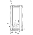
- FIG. 1 is a cross-sectional view of the liquid crystal display panel according to the first embodiment.
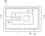
- FIG. 2 is a plan view of each sub-pixel of the TFT array substrate constituting the liquid crystal display panel according to the first embodiment.
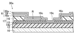
- FIG. 3 is a cross-sectional view of the TFT array substrate along the line III-III in FIG.
- FIG. 4 is an enlarged plan view of the connection region provided in each subpixel of the TFT array substrate and the vicinity thereof.
- FIG. 5 is a cross-sectional view of the TFT array substrate along the line VV in FIG.
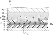
- FIG. 6 is a cross-sectional view of the liquid crystal display panel in the correction process.
- FIG. 7 is a cross-sectional view of the liquid crystal display panel of FIG. 6 after the correction process.
- FIG. 1 is a cross-sectional view of the liquid crystal display panel according to the first embodiment.
- FIG. 2 is a plan view of each sub-pixel of the TFT array substrate constituting the liquid crystal display panel according to the first embodiment.
- FIG. 8 is an enlarged plan view of the connection region provided in each subpixel of the TFT array substrate constituting the liquid crystal display panel according to Embodiment 2 and the vicinity thereof.
- FIG. 9 is an enlarged plan view of the connection region provided in each subpixel of the TFT array substrate constituting the liquid crystal display panel according to Embodiment 3 and the vicinity thereof.
- FIG. 10 is a cross-sectional view of the TFT array substrate along the line XX in FIG.
- FIG. 11 is a cross-sectional view of the TFT array substrate in the correction process according to the fourth embodiment.
- Embodiment 1 of the Invention 1 to 7 show Embodiment 1 of a liquid crystal display panel and a method for manufacturing the same according to the present invention.
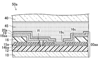
- FIG. 1 is a cross-sectional view of the liquid crystal display panel 50 of the present embodiment.
- 2 is a plan view of each subpixel P of the TFT array substrate 30a constituting the liquid crystal display panel 50
- FIG. 3 is a cross-sectional view of the TFT array substrate 30a taken along line III-III in FIG.
- It is. 4 is an enlarged plan view of the connection region R provided in each sub-pixel P of the TFT array substrate 30a and the vicinity thereof
- FIG. 5 is a TFT array along the line VV in FIG. It is sectional drawing of the board
- the liquid crystal display panel 50 includes a TFT array substrate 30a and a counter substrate 40 provided so as to face each other, a liquid crystal layer 45 provided between the TFT array substrate 30a and the counter substrate 40, The TFT array substrate 30a and the counter substrate 40 are adhered to each other, and a sealing material 46 provided in a frame shape is provided between the TFT array substrate 30a and the counter substrate 40 to enclose the liquid crystal layer 45.
- the terminal area T is defined on the surface of the TFT array substrate 30 a protruding from the counter substrate 40, but the display area D is defined on the inner side of the sealing material 46. .
- a plurality of sub-pixels P are arranged in a matrix.
- the TFT array substrate 30 a covers the transparent substrate 10, the plurality of gate lines 11 provided on the transparent substrate 10 so as to extend in parallel with each other, and the gate lines 11.
- a gate insulating film 12 provided, a plurality of source lines 14 provided on the gate insulating film 12 so as to extend in parallel to each other in a direction perpendicular to the gate lines 11, and the gate lines 11 and the source lines 14.
- the TFT 5 includes a gate electrode 11a provided on the transparent substrate 10, a gate insulating film 12 provided so as to cover the gate electrode 11a, and a gate electrode on the gate insulating film 12.
- the semiconductor layer 13 is provided in an island shape so as to overlap with 11a, and the source electrode 14a and the drain electrode 14b are provided on the semiconductor layer 13 so as to be separated from each other.
- the gate electrode 11 a is a portion where each gate line 11 protrudes laterally for each subpixel P.
- the gate electrode 11a composed of a portion protruding to the side of each gate line 11 is illustrated, but this gate electrode may be a part of the gate line 11 extending in a linear shape.
- the semiconductor layer 13 is provided on, for example, an intrinsic amorphous silicon layer (not shown) having a channel region and an intrinsic amorphous silicon layer so that the channel region is exposed, and n connected to the source electrode 14a and the drain electrode 14b, respectively. + An amorphous silicon layer (not shown).
- amorphous silicon is exemplified as the semiconductor layer 13, but the semiconductor layer 13 may be, for example, polysilicon or an In—Ga—Zn—O-based oxide semiconductor.
- the source electrode 14a is a portion in which each source line 14 protrudes laterally for each subpixel P, as shown in FIG.
- the source electrode 14a composed of a portion protruding to the side of each source line 14 is illustrated, but the source electrode may be a part of the source line 14 extending linearly.
- the drain electrode 14b is connected to the pixel electrode 20a while being insulated from the capacitor electrode 18a, that is, through a contact hole 19c formed in the capacitor insulating film 19 covering the capacitor electrode 18a. Has been.
- the capacitor electrode 18a is integrally formed over all the subpixels P, and each subpixel P has an opening 18c at the connection portion between the drain electrode 14b and the pixel electrode 20a. is doing. As shown in FIGS. 3 and 5, the capacitor electrode 18 a is opposed to the pixel electrode 20 a through the capacitor insulating film 19, thereby constituting the auxiliary capacitor 6 for each subpixel P. Further, as shown in FIG. 4, the capacitor electrode 18 a protrudes to the left middle portion of the opening 16 c of the organic insulating film 16 to be described later.
- the interlayer insulating film 17 includes an inorganic insulating film 15 provided on the transparent substrate 10 side and an organic insulating film 16 laminated on the inorganic insulating film 15.
- the organic insulating film 16 has an opening 16c at the connection portion between the drain electrode 14b and the pixel electrode 20a.
- the inorganic insulating film 15 is organically insulated. The film 16 is exposed. Then, in the opening 16c of the organic insulating film 16, as shown in FIGS.
- connection region R The hatched portion in FIG. 4 is configured.
- the pixel electrode 20a uppermost layer
- capacitor insulating film 19 the pixel electrode 20a disposed on the entire surface in the drawing is omitted.
- the counter substrate 40 includes, for example, a transparent substrate (not shown), a black matrix (not shown) provided in a lattice shape on the transparent substrate, a red layer, a green layer, and a black layer provided between the lattices of the black matrix, respectively.
- a plurality of colored layers such as a blue layer, a black matrix, a common electrode (not shown) provided to cover each colored layer, and a plurality of photo spacers (not shown) provided in a column shape on the common electrode
- an alignment film (not shown) provided so as to cover the common electrode and each photospacer.
- the liquid crystal layer 45 is made of a nematic liquid crystal material having electro-optical characteristics.
- the liquid crystal display panel 50 configured as described above applies a predetermined voltage for each subpixel P to the liquid crystal layer 45 disposed between each pixel electrode 20a on the TFT array substrate 30a and the common electrode on the counter substrate 40. By changing the alignment state of the liquid crystal layer 45, the transmittance of light transmitted through the panel is adjusted to each sub-pixel P, and an image is displayed.
- the manufacturing method of the liquid crystal display panel 50a of this embodiment includes a TFT array substrate manufacturing process, a counter substrate manufacturing process, a liquid crystal injection process, a detection process, and a correction process.
- 6 is a cross-sectional view of the liquid crystal display panel 50 in the correction process
- FIG. 7 is a cross-sectional view of the liquid crystal display panel 50a after the correction process is performed on the liquid crystal display panel 50 of FIG. .
- a molybdenum film (thickness of about 150 nm) or the like is formed on the entire transparent substrate 10 such as a glass substrate or a plastic substrate by sputtering, for example, and then photolithography, etching and etching are performed on the molybdenum film.
- the resist line is washed to form the gate line 11 and the gate electrode 11a.
- the method of forming the gate line 11 and the gate electrode 11a using the molybdenum film is exemplified.
- a metal such as an aluminum film, a tungsten film, a tantalum film, a chromium film, a titanium film, or a copper film is used.
- the gate line 11 and the gate electrode 11a may be formed using a film, an alloy film thereof, a metal nitride film, or a laminated film thereof.
- a silicon nitride film (having a thickness of about 100 nm to 600 nm) is formed on the entire substrate on which the gate line 11 and the gate electrode 11a are formed, for example, by plasma CVD (Chemical Vapor Deposition) method. 12 is formed.
- the method of forming the gate insulating film 12 using a silicon nitride film has been exemplified, but for example, a silicon oxide film (SiOx), a silicon oxynitride film (SiOxNy, x> y), nitriding oxide
- the gate insulating film 12 may be formed using a single layer film such as a silicon film (SiNxOy, x> y) or a laminated film thereof.
- an intrinsic amorphous silicon film (thickness of about 100 nm) and a phosphorus-doped n + amorphous silicon film (thickness of about 50 nm) are sequentially formed on the entire substrate on which the gate insulating film 12 is formed, for example, by plasma CVD.
- the semiconductor layer forming portion (13) is formed by performing photolithography, etching, and resist peeling cleaning on the laminated film of the intrinsic amorphous silicon film and the n + amorphous silicon film.
- a titanium film (thickness of about 20 nm to 150 nm), an aluminum film (thickness of about 50 nm to 400 nm), and the like are sequentially formed on the entire substrate on which the semiconductor layer forming portion (13) has been formed by, for example, sputtering.
- the source line 14, the source electrode 14a, and the drain electrode 14b are formed by performing photolithography, etching, and resist peeling cleaning on the metal laminated film.
- the method of forming the source line 14, the source electrode 14a, and the drain electrode 14b by using a metal laminated film of a titanium film and an aluminum film is exemplified.
- the source line 14, the source electrode 14a, and the drain electrode 14b may be formed using a metal film such as a tantalum film, a chromium film, a titanium film, or a copper film, an alloy film thereof, a metal nitride film, or a laminated film thereof. Good.
- the n + amorphous silicon film in the semiconductor layer forming portion is etched to form a channel region, and the semiconductor layer 13 and the TFT 5 including the semiconductor layer 13 are formed. .
- an inorganic insulating film (15) such as a silicon nitride film, a silicon oxide film, and a silicon nitride oxide film is formed with a thickness of about 300 nm on the entire substrate on which the TFT 5 is formed, for example, by plasma CVD.
- a photosensitive resin film made of a photosensitive acrylic resin or the like is formed on the entire substrate on which the inorganic insulating film (15) is formed, for example, by spin coating or slit coating, to a thickness of 2.0 ⁇ m to 4.0 ⁇ m. After coating to the extent, the organic insulating film 16 having the openings 16c is formed by performing exposure, development and baking on the photosensitive resin film.
- a transparent conductive film such as an ITO (IndiumInTin Oxide) film is formed on the entire substrate on which the organic insulating film 16 is formed, for example, by a sputtering method to a thickness of about 50 nm to 200 nm.
- the capacitor electrode 18a having the opening 18c is formed by performing photolithography, etching, and resist peeling cleaning.
- an inorganic insulating film such as a silicon nitride film, a silicon oxide film, or a silicon nitride oxide film is formed on the entire substrate on which the capacitor electrode 18a is formed by a plasma CVD method, for example, with a thickness of about 300 nm.
- the interlayer insulating film 17 composed of the inorganic insulating film 15 and the organic insulating film 16 is obtained by performing photolithography, etching, and resist peeling cleaning on the insulating film (19) and the previously formed inorganic insulating film (15).
- a capacitor insulating film 19 having a contact hole 19c is formed.
- the transparent conductive film is formed on the transparent conductive film.
- the pixel electrode 20a is formed by performing photolithography, etching, and resist peeling cleaning.
- an alignment film is formed by baking and rubbing the applied film.
- the TFT array substrate 30a can be manufactured as described above.
- a black colored photosensitive resin is applied to the entire transparent substrate such as a glass substrate or a plastic substrate by, for example, a spin coating method or a slit coating method, and then the coating film is exposed and developed. And by baking, a black matrix is formed to a thickness of about 1.0 ⁇ m.
- a photosensitive resin colored in red, green or blue for example, is applied to the entire substrate on which the black matrix is formed, for example, by spin coating or slit coating, and then applied to the coating film.
- a colored layer for example, a red layer
- a selected color is formed to a thickness of about 2.0 ⁇ m.
- the same process is repeated for the other two colors to form other two colored layers (for example, a green layer and a blue layer) with a thickness of about 2.0 ⁇ m.
- a common electrode is formed by forming a transparent conductive film such as an ITO film with a thickness of about 50 nm to 200 nm on the entire substrate on which the colored layers are formed, for example, by sputtering.
- a photosensitive resin film made of photosensitive acrylic resin or the like is formed to the entire substrate on which the common electrode is formed, for example, by spin coating or slit coating.
- a photo spacer is formed to a thickness of about 4.0 ⁇ m.
- an alignment film is formed by baking and rubbing the applied film.
- the counter substrate 40 can be manufactured as described above.
- ⁇ Liquid crystal injection process First, for example, after a sealing material 46 made of UV (ultraviolet) curing and thermosetting resin is printed on the surface of the counter substrate 40 manufactured in the counter substrate manufacturing process in a frame shape, A liquid crystal material is dropped inside.
- a sealing material 46 made of UV (ultraviolet) curing and thermosetting resin is printed on the surface of the counter substrate 40 manufactured in the counter substrate manufacturing process in a frame shape.
- the counter substrate 40 onto which the liquid crystal material is dropped and the TFT array substrate 30a manufactured in the TFT array substrate manufacturing process are bonded together under reduced pressure, and then the bonded body is brought to atmospheric pressure. By opening, the surface and the back surface of the bonded body are pressurized.
- the sealing material 46 is cured by heating the bonded body.
- the unnecessary part is removed by dividing the bonded body in which the sealing material 46 is cured by, for example, dicing.
- the liquid crystal display panel 50 (before inspection) can be manufactured.
- a gate inspection signal having a bias voltage of ⁇ 15 V having a bias voltage of ⁇ 10 V, a period of 16.7 msec, a pulse width of 50 ⁇ sec is input to each gate line 11, and the TFTs 5 of all subpixels P are input. Is turned on, and a source inspection signal having a potential of ⁇ 2 V whose polarity is inverted every 16.7 msec is input to each source line 14, whereby a source inspection signal is input to the pixel electrode 20 a via each TFT 5. To do.
- a common electrode inspection signal having a direct current potential of ⁇ 1 V is input to the common electrode of the counter substrate 40, thereby arranging the pixel electrode 20 a of the TFT array substrate 30 a and the common electrode of the counter substrate 40.
- a voltage to the liquid crystal layer 45 each subpixel P constituted by each pixel electrode 20a is turned on.
- the display screen changes from black display to white display.
- the sub-pixel P in which a short circuit S see a two-dot chain line in FIG.
- the pixel is not related to the on / off control of the TFT 5. Since the source inspection signal is always input to the electrode 20a, the subpixel P is detected as a bright spot on the black display screen.
- the X pixel of the drain electrode 14b is irradiated with the laser light L in the detected sub-pixel P as shown in FIGS.
- the side of the cut drain electrode 14b connected to the pixel electrode 20a is connected to the capacitor electrode 18a.
- the reference numerals of the drain electrode 14b and the capacitor electrode 18a connected to each other are 14ba and 18aa, respectively, and the reference numeral of the inorganic insulating film 15 disposed therebetween is 15a.
- the reference numeral of the TFT array substrate 30a provided with them is 30aa.
- the laser beam L is output with a spot size of about 2.5 ⁇ m ⁇ 2.5 ⁇ m from, for example, a YAG (Yttrium Aluminum Garnet) laser. If the size of the connection region R is about 5 ⁇ m ⁇ 5 ⁇ m or more, the connection region R can be corrected by irradiating the connection region R with laser light.
- the interlayer insulating film 17 between the drain electrode 14b and the capacitor electrode 18a is the inorganic insulating film 15.
- the organic insulating film 16 are sequentially stacked, and the drain electrode 14b and the capacitor electrode 18a have a connection region R that overlaps with the inorganic insulating film 15 exposed from the organic insulating film 16.
- the relatively thick organic insulating film 16 is not disposed as an insulating film that electrically insulates between the drain electrode 14b and the capacitor electrode 18a. Only 15 are arranged.
- the sub circuit P in which the short circuit S has occurred between the source electrode 14a and the drain electrode 14b is detected as a bright spot by the lighting inspection, the sub circuit P in which the short circuit S has occurred in the correction process.
- the metal of the drain electrode 14b is scattered in the interlayer insulating film 17 (inorganic insulating film 15 and organic insulating film 16).
- the electrode 14b is cut, and the drain electrode 14b and the capacitor electrode 18a are irradiated with laser light L from the transparent substrate 10 side to the connection region R where the drain electrode 14b and the capacitor electrode 18a overlap with each other through the inorganic insulating film 15, thereby comparing the metal of the drain electrode 14b. Since the thin inorganic insulating film 15 scatters and easily reaches the capacitor electrode 18a, the image of the cut drain electrode 14b is reduced. And connected to the electrode 20a side and the capacitor electrode 18a can be reliably connected. Thereby, in the sub-pixel P in which the short circuit S has occurred, the pixel electrode 20a is fixed to the potential of the capacitor electrode 18a (for example, the ground potential), and the bright spot can be turned into a black spot. Therefore, the liquid crystal display panel 50 (50a ), The drain electrode 14b (14ba) and the capacitor electrode 18a (18aa) can be reliably connected.
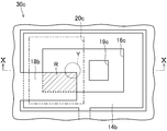
- FIG. 8 is an enlarged plan view of the connection region R provided in each sub-pixel P of the TFT array substrate 30b constituting the liquid crystal display panel of this embodiment and the vicinity thereof.
- the pixel electrode (20a) disposed on the entire surface in the drawing is omitted.
- the same parts as those in FIGS. 1 to 7 are denoted by the same reference numerals, and detailed description thereof will be omitted.
- region R was illustrated, in this embodiment, the laser beam L is irradiated.
- a method for manufacturing a liquid crystal display panel in which a part of the Y portion is included in the connection region R will be exemplified.
- the liquid crystal display panel of this embodiment is provided between the TFT array substrate 30b (see FIG. 8) and the counter substrate 40 (see FIG. 1), and the TFT array substrate 30b and the counter substrate 40 provided so as to face each other.
- the liquid crystal layer 45 (see FIG. 1), the TFT array substrate 30b and the counter substrate 40 are bonded to each other, and the liquid crystal layer 45 is provided between the TFT array substrate 30b and the counter substrate 40 in a frame shape.
- a sealing material 46 see FIG. 1).
- the TFT array substrate 30b covers the transparent substrate 10 (see FIG. 3), the plurality of gate lines 11 (see FIG. 2) provided on the transparent substrate 10 so as to extend in parallel to each other, and the gate lines 11 so as to cover them.
- a plurality of TFTs 5 (see FIGS. 2 and 3) provided at each intersection of each gate line 11 and each source line 14, and an interlayer insulating film 17 (see FIG. 2 and FIG. 3) provided so as to cover each TFT 5 and each source line 14. 3), a capacitor electrode 18b (see FIG.
- a capacitor insulating film 19 (see FIG. 3) provided so as to cover the capacitor electrode 18b, and a capacitor insulating film 19 Set in a matrix on top It is provided with a plurality of pixel electrodes 20a which are connected to each TFT 5 (see FIGS. 2 and 3), an alignment film provided so as to cover the pixel electrodes 20a and (not shown).
- the capacitor electrode 18b protrudes from the lower left portion of the opening 16c of the organic insulating film 16 in the drawing. Then, in the opening 16c of the organic insulating film 16, as shown in FIG. 8, the protruding portions of the drain electrode 14b and the capacitor electrode 18b overlap with each other through the inorganic insulating film 15, so that the connection region R (in the drawing) (See hatched part).
- the TFT array substrate 30b of this embodiment and the liquid crystal display panel including the same can be manufactured by changing the pattern shape of the capacitor electrode 18a in the TFT array substrate manufacturing process of Embodiment 1 described above. And a detection process is performed with respect to the manufactured liquid crystal display panel provided with the TFT array substrate 30b similarly to the said Embodiment 1, and when the short circuit S is detected, a correction process will be performed. Specifically, in the correction process, as shown in FIG. 2, in the subpixel P in which the short circuit S is detected, the X portion of the drain electrode 14b is irradiated with the laser light L as shown in FIG.
- the drain electrode 14b and the capacitor electrode 18b of the TFT array substrate 30b are similar to the first embodiment.
- the interlayer insulating film 17 is formed by sequentially laminating the inorganic insulating film 15 and the organic insulating film 16, and the drain electrode 14 b and the capacitor electrode 18 b are connected to each other through the inorganic insulating film 15 exposed from the organic insulating film 16. Since R is provided, the drain electrode 14b and the capacitor electrode 18b can be reliably connected in the defect correction by blackening of the liquid crystal display panel.
- the laser light L is irradiated to the end of the connection region R and the outside of the connection region R adjacent thereto in the correction process.
- the irradiation of the laser beam L is not concentrated only on the connection region R, excessive scattering of the metal of the drain electrode 14b can be suppressed, and the drain electrode 14b and the capacitor electrode 18b can be more reliably connected. it can.
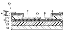
- FIG. 9 is an enlarged plan view of the connection region R provided in each subpixel P of the TFT array substrate 30c constituting the liquid crystal display panel of this embodiment and the vicinity thereof, and FIG. FIG. 11 is a cross-sectional view of the TFT array substrate 30c along the line X.
- the TFT array substrates 30a and 30b in which the pixel electrode 20a overlaps with the connection region R are illustrated, but in this embodiment, the TFT array substrate 30c in which the pixel electrode 20b does not overlap with the connection region R is illustrated. To do.
- the liquid crystal display panel of this embodiment includes a TFT array substrate 30c (see FIGS. 9 and 10) and a counter substrate 40 (see FIG. 1) provided so as to face each other, and between the TFT array substrate 30c and the counter substrate 40.
- the liquid crystal layer 45 (see FIG. 1) provided on the TFT array substrate 30c and the counter substrate 40 are bonded to each other, and the liquid crystal layer 45 is enclosed between the TFT array substrate 30c and the counter substrate 40 in a frame shape.
- the sealing material 46 (refer FIG. 1) provided is provided.
- the TFT array substrate 30c includes a transparent substrate 10, a plurality of gate lines 11 (see FIG. 2) provided on the transparent substrate 10 so as to extend in parallel with each other, and each gate line.
- a gate insulating film 12 provided so as to cover 11, a plurality of source lines 14 provided on the gate insulating film 12 so as to extend in parallel to each other in a direction orthogonal to the gate lines 11 (see FIG. 2),
- a plurality of TFTs 5 (see FIGS. 2 and 3) provided at each intersection of each gate line 11 and each source line 14, and an interlayer insulating film 17 provided so as to cover each TFT 5 and each source line 14.
- the capacitor electrode 18b protrudes from the lower left portion of the opening 16c of the organic insulating film 16 in the drawing.
- the opening 16c of the organic insulating film 16 as shown in FIGS. 9 and 10, the protruding portions of the drain electrode 14b and the capacitor electrode 18b overlap with each other through the inorganic insulating film 15, thereby connecting regions R ( The hatched portion in FIG. 9) is configured.
- an opening 20c of the pixel electrode 20b is provided so as to overlap the connection region R.
- the opening 20c of the pixel electrode 20b is configured to function as a structure for regulating the alignment of the liquid crystal layer 45.
- the TFT array substrate 30c of this embodiment and the liquid crystal display panel including the same can be manufactured by changing the pattern shape of the capacitor electrode 18a and the pixel electrode 20a in the TFT array substrate manufacturing process of Embodiment 1 described above. . And a detection process is performed with respect to the manufactured liquid crystal display panel provided with the TFT array substrate 30c like the said Embodiment 1, and when the short circuit S is detected, a correction process will be performed. Specifically, in the correction process, as shown in FIG. 2, in the subpixel P in which the short circuit S is detected, the X portion of the drain electrode 14b is irradiated with the laser light L as shown in FIG. In addition to cutting the drain electrode 14b at the X portion, as shown in FIG. 9, by irradiating the Y portion including the outside of the connection region R adjacent to the upper right portion of the connection region R in the drawing, The side of the cut drain electrode 14b connected to the pixel electrode 20b is connected to the capacitor electrode 18b.
- the drain electrode 14b and the capacitor electrode in the TFT array substrate 30c as in the first and second embodiments.
- An interlayer insulating film 17 between 18 b is formed by sequentially laminating the inorganic insulating film 15 and the organic insulating film 16, and the drain electrode 14 b and the capacitor electrode 18 b overlap with each other through the inorganic insulating film 15 exposed from the organic insulating film 16. Since the connection region R is provided, the drain electrode 14b and the capacitor electrode 18b can be reliably connected in the defect correction by the blackening of the liquid crystal display panel.
- the laser beam L is irradiated to the end of the connection region R and the outside of the connection region R adjacent thereto in the correction process.
- the irradiation of the laser beam L is not concentrated only on the connection region R, excessive scattering of the metal of the drain electrode 14b can be suppressed, and the drain electrode 14b and the capacitor electrode 18b can be more reliably connected. it can.
- each pixel electrode 20b overlaps the connection region R as a structure for regulating the alignment of the liquid crystal layer 45.
- the opening 20c is provided, damage to the pixel electrode 20b due to the irradiation of the laser light L to the connection region R can be suppressed.
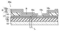
- FIG. 11 shows an embodiment of a TFT array substrate and a manufacturing method thereof according to the present invention. Specifically, FIG. 11 is a cross-sectional view of the TFT array substrate 30a in the correction process of this embodiment.
- the liquid crystal display panel that performs the detection process and the correction process in the panel state and the manufacturing method thereof are exemplified.
- the TFT array substrate 30a that performs the detection process and the correction process in the substrate state and the manufacture thereof. The method is illustrated.
- the TFT array substrate 30a of the present embodiment is the same as the TFT array substrate 30a of the first embodiment, but may be the TFT array substrate 30b of the second embodiment or the TFT array substrate 30c of the third embodiment.
- the TFT array substrate 30a of the present embodiment includes, for example, subpixels P in which a short circuit S has occurred between the source electrode 14a and the drain electrode 14b by optical inspection using a CCD (Charge Coupled Device) camera or inspection using a charge detection method. By detecting, a detection process is performed, and when the short circuit S is detected, a correction process is performed. Specifically, in the correction process, in the sub-pixel P in which the short circuit S is detected, the drain electrode 14b is cut at the X portion by irradiating the X portion (see FIG. 2) of the drain electrode 14b with the laser light L. At the same time, as shown in FIG. 11, by irradiating the Y portion (see FIG. 4) of the connection region R with laser light L, the side of the cut drain electrode 14b connected to the pixel electrode 20a and the capacitor electrode 18a Are connected (see TFT array substrate 30aa in FIG. 7).
- CCD Charge Coupled Device
- the interlayer insulating film 17 between the drain electrode 14b and the capacitor electrode 18a is formed by sequentially stacking the inorganic insulating film 15 and the organic insulating film 16. Since the drain electrode 14b and the capacitor electrode 18a are provided with the connection region R that overlaps with each other through the inorganic insulating film 15 exposed from the organic insulating film 16, the drain electrode 14b and the capacitor electrode 18a overlap with each other. In this case, only the relatively thin inorganic insulating film 15 is disposed without the relatively thick organic insulating film 16 as the insulating film for electrically insulating the drain electrode 14b and the capacitor electrode 18a.
- the short circuit S in the correction process when the sub-pixel P in which the short circuit S has occurred between the source electrode 14a and the drain electrode 14b is detected by the optical inspection or the inspection by the charge detection method in the detection process, the short circuit S in the correction process.
- the metal of the drain electrode 14b is scattered in the interlayer insulating film 17 (inorganic insulating film 15 and organic insulating film 16) by irradiating the drain electrode 14b with the laser light L from the transparent substrate 10 side.
- the drain electrode 14b is cut, and the drain electrode 14b and the capacitor electrode 18a are irradiated with laser light L from the transparent substrate 10 side to the connection region R where the drain electrode 14b and the capacitor electrode 18a overlap each other through the inorganic insulating film 15.
- the metal is scattered in the relatively thin inorganic insulating film 15 and easily reaches the capacitor electrode 18a. It is possible to reliably connect the electrode 14b of the pixel electrode 20a connected to the side and the capacitor electrode 18a.
- the pixel electrode 20a is fixed to the potential of the capacitor electrode 18a (for example, the ground potential) and becomes a black spot.
- the drain electrode 14b and the capacitor electrode 18a can be reliably connected.
- the correction method for cutting the drain electrode 14b is exemplified.
- the source electrode 14a can be cut, the source electrode 14a is cut at its base instead of cutting the drain electrode 14b. May be.
- the TFT is exemplified as the switching element.
- the present invention can also be applied to other three-terminal switching elements such as MOSFET (Metal / Oxide / Semiconductor / Field / Effect / Transistor).
- each pixel has three subpixels (red, green, and blue) is illustrated.
- each pixel has four or more subpixels (for example, red, green, and blue).
- the present invention can also be applied to liquid crystal display panels having green, blue, white, red, green, blue, yellow, and the like.
- an array substrate in which a plurality of subpixels are arranged in a matrix and a liquid crystal display panel including the same are exemplified.
- the present invention is an array in which a plurality of subpixels are arranged in a delta shape.
- the present invention can also be applied to a substrate and a liquid crystal display panel including the substrate.
- the TFT array substrate in which the TFT electrode connected to the pixel electrode is used as the drain electrode is illustrated.
- the TFT electrode connected to the pixel electrode is referred to as the source electrode. It can also be applied to a substrate.
- the present invention is useful for a display panel having an auxiliary capacitor because the drain electrode and the capacitor electrode are reliably connected in defect correction by blackening.
Landscapes
- Physics & Mathematics (AREA)
- Engineering & Computer Science (AREA)
- Nonlinear Science (AREA)
- General Physics & Mathematics (AREA)
- Microelectronics & Electronic Packaging (AREA)
- Power Engineering (AREA)
- Chemical & Material Sciences (AREA)
- Crystallography & Structural Chemistry (AREA)
- Mathematical Physics (AREA)
- Optics & Photonics (AREA)
- Computer Hardware Design (AREA)
- Condensed Matter Physics & Semiconductors (AREA)
- Geometry (AREA)
- Manufacturing & Machinery (AREA)
- Liquid Crystal (AREA)
- Thin Film Transistor (AREA)
- Devices For Indicating Variable Information By Combining Individual Elements (AREA)
Abstract
Description
図1~図7は、本発明に係る液晶表示パネル及びその製造方法の実施形態1を示している。具体的に、図1は、本実施形態の液晶表示パネル50の断面図である。また、図2は、液晶表示パネル50を構成するTFTアレイ基板30aの各副画素Pの平面図であり、図3は、図2中のIII-III線に沿ったTFTアレイ基板30aの断面図である。さらに、図4は、TFTアレイ基板30aの各副画素Pに設けられた接続領域R及びその近傍を拡大した平面図であり、図5は、図4中のV-V線に沿ったTFTアレイ基板30aの断面図である。
まず、ガラス基板やプラスチック基板などの透明基板10の基板全体に、例えば、スパッタリング法により、モリブデン膜(厚さ150nm程度)などを成膜した後に、そのモリブデン膜に対して、フォトリソグラフィ、エッチング及びレジストの剥離洗浄を行うことにより、ゲート線11及びゲート電極11aを形成する。なお、本実施形態では、モリブデン膜を用いてゲート線11及びゲート電極11aを形成する方法を例示したが、例えば、アルミニウム膜、タングステン膜、タンタル膜、クロム膜、チタン膜、銅膜などの金属膜、その合金膜や金属窒化膜、又はそれらの積層膜を用いて、ゲート線11及びゲート電極11aを形成してもよい。
まず、ガラス基板やプラスチック基板などの透明基板の基板全体に、例えば、スピンコート法又はスリットコート法により、黒色に着色された感光性樹脂を塗布した後に、その塗布膜に対して、露光、現像及びベーキングを行うことにより、ブラックマトリクスを厚さ1.0μm程度に形成する。
まず、例えば、上記対向基板製造工程で製造された対向基板40の表面に、UV(ultraviolet)硬化及び熱硬化の併用型樹脂などからなるシール材46を枠状に印刷した後に、シール材46の内側に液晶材料を滴下する。
上記製造された液晶表示パネル50において、各ゲート線11に、バイアス電圧-10V、周期16.7msec、パルス幅50μsecの+15Vのパルス電圧のゲート検査信号を入力して、全ての副画素PのTFT5をオン状態にすると共に、各ソース線14に、16.7msec毎に極性が反転する±2Vの電位のソース検査信号を入力することにより、各TFT5を介して画素電極20aにソース検査信号を入力する。そして、同時に、対向基板40の共通電極に直流で-1Vの電位の共通電極検査信号を入力することにより、TFTアレイ基板30aの各画素電極20aと対向基板40の共通電極との間に配置する液晶層45に電圧を印加して、各画素電極20aにより構成される各副画素Pが点灯状態になる。このとき、例えば、ノーマリブラックモード(電圧無印加時に黒表示)の液晶表示パネル50では、表示画面が黒表示から白表示となる。ここで、膜残りなどにより、ソース電極14a及びドレイン電極14bの間で短絡S(図2中の2点鎖線参照)が発生した副画素Pでは、TFT5のオン/オフ制御に関係せず、画素電極20aにソース検査信号が常に入力されるので、その副画素Pは、黒表示の表示画面において輝点として検出される。
上記検出工程で短絡Sが検出された場合には、その検出された副画素Pにおいて、図2及び図6に示すように、ドレイン電極14bのX部にレーザー光Lを照射することにより、ドレイン電極14bをX部で切断すると共に、接続領域RのY部にレーザー光Lを照射することにより、切断されたドレイン電極14bの画素電極20aに接続された側と容量電極18aとを接続する。ここで、図7の修正工程後の液晶表示パネル50aでは、互いに接続されたドレイン電極14b及び容量電極18aの符号をそれぞれ14ba及び18aaとし、それらの間に配置する無機絶縁膜15の符号を15aとし、それらを備えたTFTアレイ基板30aの符号を30aaとしている。また、レーザー光Lは、例えば、YAG(Yttrium Aluminium Garnet)レーザーなどから、2.5μm×2.5μm程度のスポットサイズで出力されたものである。なお、接続領域Rは、その大きさが5μm×5μm程度以上あれば、接続領域Rにレーザー光を照射して、修正可能である。
図8は、本実施形態の液晶表示パネルを構成するTFTアレイ基板30bの各副画素Pに設けられた接続領域R及びその近傍を拡大した平面図である。ここで、図8では、図4と同様に、図中全面に配置する画素電極(20a)が省略されている。なお、以下の各実施形態において、図1~図7と同じ部分については同じ符号を付して、その詳細な説明を省略する。
図9は、本実施形態の液晶表示パネルを構成するTFTアレイ基板30cの各副画素Pに設けられた接続領域R及びその近傍を拡大した平面図であり、図10は、図9中のX-X線に沿ったTFTアレイ基板30cの断面図である。
図11は、本発明に係るTFTアレイ基板及びその製造方法の実施形態を示している。具体的に、図11は、本実施形態の修正工程におけるTFTアレイ基板30aの断面図である。
P 副画素
R 接続領域
S 短絡
5 TFT(スイッチング素子)
6 補助容量
10 透明基板
12 ゲート絶縁膜
14a ソース電極
14b ドレイン電極
15,15a 無機絶縁膜
16 有機絶縁膜
17 層間絶縁膜
18a,18b 容量電極
19 容量絶縁膜
20a,20b 画素電極
20c 開口部
30a,30aa,30b,30c TFTアレイ基板
40 対向基板
45 液晶層
50,50a 液晶表示パネル
Claims (7)
- 複数の副画素と、
互いに対向するように設けられたアレイ基板及び対向基板と、
上記アレイ基板及び対向基板の間に設けられた液晶層とを備え、
上記アレイ基板が、
透明基板に上記各副画素毎にそれぞれ設けられ、各々、互いに離間するように配置されたソース電極及びドレイン電極を有する複数のスイッチング素子と、
上記各スイッチング素子を覆うように設けられ、無機絶縁膜及び有機絶縁膜が順に積層された層間絶縁膜と、
上記層間絶縁膜上に設けられた容量電極と、
上記容量電極を覆うように設けられた容量絶縁膜と、
上記容量絶縁膜上に設けられ、上記容量電極に対向して上記各副画素毎に補助容量を構成し、該容量電極と絶縁状態で上記各スイッチング素子のドレイン電極にそれぞれ接続された複数の画素電極とを備えた液晶表示パネルであって、
上記アレイ基板には、上記ドレイン電極及び容量電極が上記有機絶縁膜から露出する上記無機絶縁膜を介して互いに重なる接続領域が設けられていることを特徴とする液晶表示パネル。 - 請求項1に記載された液晶表示パネルにおいて、
上記各画素電極には、上記接続領域に重なるように開口部が設けられていることを特徴とする液晶表示パネル。 - 請求項1に記載された液晶表示パネルにおいて、
上記アレイ基板の上記接続領域では、上記透明基板上にゲート絶縁膜、上記ドレイン電極、無機絶縁膜、容量電極、容量絶縁膜及び各画素電極が順に積層されていることを特徴とする液晶表示パネル。 - 複数の副画素と、
互いに対向するように設けられたアレイ基板及び対向基板と、
上記アレイ基板及び対向基板の間に設けられた液晶層とを備え、
上記アレイ基板が、
透明基板に上記各副画素毎にそれぞれ設けられ、各々、互いに離間するように配置されたソース電極及びドレイン電極を有する複数のスイッチング素子と、
上記各スイッチング素子を覆うように設けられ、無機絶縁膜及び有機絶縁膜が順に積層された層間絶縁膜と、
上記層間絶縁膜上に設けられた容量電極と、
上記容量電極を覆うように設けられた容量絶縁膜と、
上記容量絶縁膜上に設けられ、上記容量電極に対向して上記各副画素毎に補助容量を構成し、該容量電極と絶縁状態で上記各スイッチング素子のドレイン電極にそれぞれ接続された複数の画素電極とを備え、
上記アレイ基板には、上記ドレイン電極及び容量電極が上記有機絶縁膜から露出する上記無機絶縁膜を介して互いに重なる接続領域が設けられた液晶表示パネルを製造する方法であって、
上記複数の副画素において、上記ソース電極及びドレイン電極の間で短絡が発生した副画素を検出する検出工程と、
上記検出工程で短絡が検出された副画素において、上記ドレイン電極にレーザー光を上記透明基板側から照射して該ドレイン電極を切断すると共に、上記接続領域にレーザー光を上記透明基板側から照射して、該切断されたドレイン電極の上記各画素電極に接続された側と上記容量電極とを接続する修正工程とを備えることを特徴とする液晶表示パネルの製造方法。 - 請求項4に記載された液晶表示パネルの製造方法において、
上記修正工程では、上記接続領域の端部及び該端部に隣接する該接続領域の外部に上記レーザー光を照射することを特徴とする液晶表示パネルの製造方法。 - 複数の副画素と、
透明基板に上記各副画素毎にそれぞれ設けられ、各々、互いに離間するように配置されたソース電極及びドレイン電極を有する複数のスイッチング素子と、
上記各スイッチング素子を覆うように設けられ、無機絶縁膜及び有機絶縁膜が順に積層された層間絶縁膜と、
上記層間絶縁膜上に設けられた容量電極と、
上記容量電極を覆うように設けられた容量絶縁膜と、
上記容量絶縁膜上に設けられ、上記容量電極に対向して上記各副画素毎に補助容量を構成し、該容量電極と絶縁状態で上記各スイッチング素子のドレイン電極にそれぞれ接続された複数の画素電極とを備えたアレイ基板であって、
上記ドレイン電極及び容量電極が上記有機絶縁膜から露出する上記無機絶縁膜を介して互いに重なる接続領域を備えていることを特徴とするアレイ基板。 - 複数の副画素と、
透明基板に上記各副画素毎にそれぞれ設けられ、各々、互いに離間するように配置されたソース電極及びドレイン電極を有する複数のスイッチング素子と、
上記各スイッチング素子を覆うように設けられ、無機絶縁膜及び有機絶縁膜が順に積層された層間絶縁膜と、
上記層間絶縁膜上に設けられた容量電極と、
上記容量電極を覆うように設けられた容量絶縁膜と、
上記容量絶縁膜上に設けられ、上記容量電極に対向して上記各副画素毎に補助容量を構成し、該容量電極と絶縁状態で上記各スイッチング素子のドレイン電極にそれぞれ接続された複数の画素電極と、
上記ドレイン電極及び容量電極が上記有機絶縁膜から露出する上記無機絶縁膜を介して互いに重なるように設けられた接続領域とを備えたアレイ基板を製造する方法であって、
上記複数の副画素において、上記ソース電極及びドレイン電極の間で短絡が発生した副画素を検出する検出工程と、
上記検出工程で短絡が検出された副画素において、上記ドレイン電極にレーザー光を上記透明基板側から照射して該ドレイン電極を切断すると共に、上記接続領域にレーザー光を上記透明基板側から照射して、該切断されたドレイン電極の上記各画素電極に接続された側と上記容量電極とを接続する修正工程とを備えることを特徴とするアレイ基板の製造方法。
Priority Applications (5)
| Application Number | Priority Date | Filing Date | Title |
|---|---|---|---|
| EP20120741701 EP2672317B1 (en) | 2011-01-31 | 2012-01-24 | Liquid crystal display panel and production method for same |
| US13/884,704 US8629948B2 (en) | 2011-01-31 | 2012-01-24 | Liquid crystal display panel and method for fabricating same, and array substrate and method for fabricating same |
| CN201280003813.5A CN103229095B (zh) | 2011-01-31 | 2012-01-24 | 液晶显示面板及其制造方法和阵列基板及其制造方法 |
| KR1020137012378A KR101311693B1 (ko) | 2011-01-31 | 2012-01-24 | 액정표시패널 및 그 제조방법, 그리고 어레이 기판 및 그 제조방법 |
| JP2012555726A JP5243664B2 (ja) | 2011-01-31 | 2012-01-24 | 液晶表示パネル及びその製造方法、並びにアレイ基板及びその製造方法 |
Applications Claiming Priority (2)
| Application Number | Priority Date | Filing Date | Title |
|---|---|---|---|
| JP2011018806 | 2011-01-31 | ||
| JP2011-018806 | 2011-01-31 |
Publications (1)
| Publication Number | Publication Date |
|---|---|
| WO2012105180A1 true WO2012105180A1 (ja) | 2012-08-09 |
Family
ID=46602407
Family Applications (1)
| Application Number | Title | Priority Date | Filing Date |
|---|---|---|---|
| PCT/JP2012/000420 WO2012105180A1 (ja) | 2011-01-31 | 2012-01-24 | 液晶表示パネル及びその製造方法、並びにアレイ基板及びその製造方法 |
Country Status (7)
| Country | Link |
|---|---|
| US (1) | US8629948B2 (ja) |
| EP (1) | EP2672317B1 (ja) |
| JP (1) | JP5243664B2 (ja) |
| KR (1) | KR101311693B1 (ja) |
| CN (1) | CN103229095B (ja) |
| TW (1) | TWI415239B (ja) |
| WO (1) | WO2012105180A1 (ja) |
Cited By (5)
| Publication number | Priority date | Publication date | Assignee | Title |
|---|---|---|---|---|
| WO2015071989A1 (ja) * | 2013-11-14 | 2015-05-21 | 堺ディスプレイプロダクト株式会社 | 回路基板及び表示装置 |
| JP2016075865A (ja) * | 2014-10-09 | 2016-05-12 | 三菱電機株式会社 | アレイ基板およびこれを備える液晶表示パネル |
| JP2018514801A (ja) * | 2015-03-25 | 2018-06-07 | 深▲セン▼市華星光電技術有限公司 | 液晶表示装置、液晶ディスプレー及びその製造方法、暗点化方法 |
| JP2019514075A (ja) * | 2016-05-11 | 2019-05-30 | 深▲せん▼市華星光電技術有限公司Shenzhen China Star Optoelectronics Technology Co., Ltd. | Tft基板の断線修復方法 |
| JP2020086089A (ja) * | 2018-11-22 | 2020-06-04 | 株式会社ジャパンディスプレイ | 表示装置 |
Families Citing this family (10)
| Publication number | Priority date | Publication date | Assignee | Title |
|---|---|---|---|---|
| KR20140118005A (ko) * | 2013-03-27 | 2014-10-08 | 삼성디스플레이 주식회사 | 유기 발광 표시 장치 및 그 제조 방법 |
| KR102253966B1 (ko) * | 2013-12-09 | 2021-05-18 | 엘지디스플레이 주식회사 | 유기전계 발광표시장치, 이의 제조방법 및 검사방법 |
| JP6451054B2 (ja) * | 2014-01-23 | 2019-01-16 | 凸版印刷株式会社 | 薄膜トランジスタアレイ、その製造方法及び画像表示装置 |
| KR20150137218A (ko) * | 2014-05-28 | 2015-12-09 | 삼성디스플레이 주식회사 | 액정표시장치 및 이의 제조 방법 |
| CN105487315A (zh) * | 2016-01-19 | 2016-04-13 | 武汉华星光电技术有限公司 | Tft阵列基板 |
| US20200124891A1 (en) * | 2017-01-16 | 2020-04-23 | Sharp Kabushiki Kaisha | Active matrix substrate, liquid crystal display panel, and method for manufacturing liquid crystal display panel |
| KR102193700B1 (ko) * | 2018-07-11 | 2020-12-21 | 엘지전자 주식회사 | 반도체 발광소자를 이용한 디스플레이 장치 |
| CN109728000B (zh) * | 2019-01-02 | 2021-01-15 | 京东方科技集团股份有限公司 | 一种透明显示基板和显示面板 |
| CN111430383B (zh) | 2020-05-20 | 2023-04-28 | 合肥鑫晟光电科技有限公司 | 阵列基板及其制作方法、显示装置 |
| CN112349205B (zh) * | 2020-10-26 | 2022-09-27 | 京东方科技集团股份有限公司 | 一种阵列基板及其维修方法和显示面板 |
Citations (4)
| Publication number | Priority date | Publication date | Assignee | Title |
|---|---|---|---|---|
| JPH04256362A (ja) * | 1991-02-08 | 1992-09-11 | Sanyo Electric Co Ltd | 表示装置及びその救済方法 |
| JPH04324819A (ja) * | 1991-04-25 | 1992-11-13 | Seiko Epson Corp | アクティブマトリックス表示体の画素欠陥修正方法及びその表示体 |
| JPH09179143A (ja) | 1995-12-27 | 1997-07-11 | Sharp Corp | 液晶表示装置における欠陥画素修正方法 |
| WO2010146747A1 (ja) * | 2009-06-19 | 2010-12-23 | シャープ株式会社 | アクティブマトリクス基板、液晶パネル、液晶表示装置、液晶表示ユニット、テレビジョン受像機 |
Family Cites Families (8)
| Publication number | Priority date | Publication date | Assignee | Title |
|---|---|---|---|---|
| KR970011972A (ko) * | 1995-08-11 | 1997-03-29 | 쯔지 하루오 | 투과형 액정 표시 장치 및 그 제조 방법 |
| KR101006434B1 (ko) * | 2003-06-26 | 2011-01-06 | 삼성전자주식회사 | 박막 트랜지스터 표시판 및 이를 포함하는 액정 표시장치의 수리 방법 |
| JP4882662B2 (ja) * | 2006-01-12 | 2012-02-22 | セイコーエプソン株式会社 | 電気光学装置及び電子機器 |
| US7855757B2 (en) * | 2006-07-28 | 2010-12-21 | Samsung Electronics Co., Ltd. | Liquid crystal display, method of manufacturing the same, and method of repairing the same |
| KR101211087B1 (ko) * | 2006-11-30 | 2012-12-12 | 삼성디스플레이 주식회사 | 박막 트랜지스터 기판 및 이를 포함하는 표시 장치 |
| US8446539B2 (en) * | 2007-03-13 | 2013-05-21 | Sharp Kabushiki Kaisha | Display panel and display apparatus |
| JP2009163214A (ja) * | 2007-11-02 | 2009-07-23 | Epson Imaging Devices Corp | 液晶表示装置 |
| TWI392946B (zh) * | 2009-12-18 | 2013-04-11 | Au Optronics Corp | 畫素結構 |
-
2012
- 2012-01-24 KR KR1020137012378A patent/KR101311693B1/ko not_active IP Right Cessation
- 2012-01-24 US US13/884,704 patent/US8629948B2/en not_active Expired - Fee Related
- 2012-01-24 WO PCT/JP2012/000420 patent/WO2012105180A1/ja active Application Filing
- 2012-01-24 EP EP20120741701 patent/EP2672317B1/en not_active Not-in-force
- 2012-01-24 CN CN201280003813.5A patent/CN103229095B/zh not_active Expired - Fee Related
- 2012-01-24 JP JP2012555726A patent/JP5243664B2/ja active Active
- 2012-01-31 TW TW101103118A patent/TWI415239B/zh not_active IP Right Cessation
Patent Citations (4)
| Publication number | Priority date | Publication date | Assignee | Title |
|---|---|---|---|---|
| JPH04256362A (ja) * | 1991-02-08 | 1992-09-11 | Sanyo Electric Co Ltd | 表示装置及びその救済方法 |
| JPH04324819A (ja) * | 1991-04-25 | 1992-11-13 | Seiko Epson Corp | アクティブマトリックス表示体の画素欠陥修正方法及びその表示体 |
| JPH09179143A (ja) | 1995-12-27 | 1997-07-11 | Sharp Corp | 液晶表示装置における欠陥画素修正方法 |
| WO2010146747A1 (ja) * | 2009-06-19 | 2010-12-23 | シャープ株式会社 | アクティブマトリクス基板、液晶パネル、液晶表示装置、液晶表示ユニット、テレビジョン受像機 |
Non-Patent Citations (1)
| Title |
|---|
| See also references of EP2672317A4 * |
Cited By (13)
| Publication number | Priority date | Publication date | Assignee | Title |
|---|---|---|---|---|
| CN105745698B (zh) * | 2013-11-14 | 2019-06-18 | 堺显示器制品株式会社 | 电路基板和显示装置 |
| CN105745698A (zh) * | 2013-11-14 | 2016-07-06 | 堺显示器制品株式会社 | 电路基板和显示装置 |
| JPWO2015071989A1 (ja) * | 2013-11-14 | 2017-03-09 | 堺ディスプレイプロダクト株式会社 | 回路基板及び表示装置 |
| US10031388B2 (en) | 2013-11-14 | 2018-07-24 | Sakai Display Products Corporation | Circuit board and display apparatus |
| WO2015071989A1 (ja) * | 2013-11-14 | 2015-05-21 | 堺ディスプレイプロダクト株式会社 | 回路基板及び表示装置 |
| JP2016075865A (ja) * | 2014-10-09 | 2016-05-12 | 三菱電機株式会社 | アレイ基板およびこれを備える液晶表示パネル |
| JP2018514801A (ja) * | 2015-03-25 | 2018-06-07 | 深▲セン▼市華星光電技術有限公司 | 液晶表示装置、液晶ディスプレー及びその製造方法、暗点化方法 |
| JP2019514075A (ja) * | 2016-05-11 | 2019-05-30 | 深▲せん▼市華星光電技術有限公司Shenzhen China Star Optoelectronics Technology Co., Ltd. | Tft基板の断線修復方法 |
| JP2020086089A (ja) * | 2018-11-22 | 2020-06-04 | 株式会社ジャパンディスプレイ | 表示装置 |
| JP7160334B2 (ja) | 2018-11-22 | 2022-10-25 | 株式会社ジャパンディスプレイ | 表示装置 |
| JP2023009044A (ja) * | 2018-11-22 | 2023-01-19 | 株式会社ジャパンディスプレイ | 表示装置 |
| JP7367160B2 (ja) | 2018-11-22 | 2023-10-23 | 株式会社ジャパンディスプレイ | 表示装置 |
| US11934057B2 (en) | 2018-11-22 | 2024-03-19 | Japan Display Inc. | Display device including a liquid crystal layer including polymers and liquid crystal molecules switching between a scattering state and a light transmitting state |
Also Published As
| Publication number | Publication date |
|---|---|
| EP2672317B1 (en) | 2015-04-29 |
| TW201236129A (en) | 2012-09-01 |
| TWI415239B (zh) | 2013-11-11 |
| CN103229095A (zh) | 2013-07-31 |
| US20130235292A1 (en) | 2013-09-12 |
| JPWO2012105180A1 (ja) | 2014-07-03 |
| EP2672317A4 (en) | 2014-08-20 |
| EP2672317A1 (en) | 2013-12-11 |
| KR101311693B1 (ko) | 2013-09-26 |
| US8629948B2 (en) | 2014-01-14 |
| CN103229095B (zh) | 2015-11-25 |
| KR20130062375A (ko) | 2013-06-12 |
| JP5243664B2 (ja) | 2013-07-24 |
Similar Documents
| Publication | Publication Date | Title |
|---|---|---|
| JP5243664B2 (ja) | 液晶表示パネル及びその製造方法、並びにアレイ基板及びその製造方法 | |
| US8159641B2 (en) | Array substrate having common electrode with slits that overlap data lines, and liquid crystal display apparatus having the array substrate | |
| KR101320494B1 (ko) | 수평전계방식 액정표시장치 및 그 제조방법 | |
| US8908116B2 (en) | Liquid crystal display device | |
| WO2013099155A1 (ja) | アクティブマトリクス基板及びそれを備えた液晶表示パネル | |
| US8350975B2 (en) | Array substrate and method for manufacturing the same | |
| US20130321719A1 (en) | Electronic device and method for manufacturing same | |
| WO2013171989A1 (ja) | アレイ基板及びそれを備えた液晶表示パネル | |
| US9664956B2 (en) | Liquid crystal display and manufacturing method thereof | |
| US9780127B2 (en) | Liquid crystral display and manufacturing method thereof | |
| US20200012137A1 (en) | Substrate for display device, display device, and method of producing substrate for display device | |
| US9354479B2 (en) | Liquid-crystal panel and manufacturing method thereof | |
| JP5379790B2 (ja) | アクティブマトリクス基板及びそれを備えた液晶表示パネル並びにアクティブマトリクス基板の製造方法 | |
| KR101432570B1 (ko) | 횡전계방식 액정표시장치 및 그 제조방법 | |
| US20160195789A1 (en) | Liquid crystal display | |
| JP2010165866A (ja) | 薄膜トランジスタ基板の製造方法 | |
| JP2002341330A (ja) | 液晶表示装置及び液晶表示装置の製造方法 | |
| JP2003107444A (ja) | 液晶表示装置 | |
| JP2003066435A (ja) | 液晶表示装置及び液晶表示装置の製造方法 | |
| JP2003222877A (ja) | 液晶表示装置及びその製造方法 | |
| JP2003029270A (ja) | 液晶表示装置及び液晶表示装置の製造方法 | |
| WO2013099191A1 (ja) | アクティブマトリクス基板及び液晶表示装置 | |
| KR20080000208A (ko) | 액정표시장치 및 그 제조방법 | |
| WO2011080987A1 (ja) | 液晶パネル用アレイ基板と該基板を備える液晶表示装置 | |
| JP2011221295A (ja) | 液晶パネル用アレイ基板と該基板を備える液晶表示装置 |
Legal Events
| Date | Code | Title | Description |
|---|---|---|---|
| 121 | Ep: the epo has been informed by wipo that ep was designated in this application |
Ref document number: 12741701 Country of ref document: EP Kind code of ref document: A1 |
|
| WWE | Wipo information: entry into national phase |
Ref document number: 2012555726 Country of ref document: JP |
|
| WWE | Wipo information: entry into national phase |
Ref document number: 13884704 Country of ref document: US |
|
| ENP | Entry into the national phase |
Ref document number: 20137012378 Country of ref document: KR Kind code of ref document: A |
|
| WWE | Wipo information: entry into national phase |
Ref document number: 2012741701 Country of ref document: EP |
|
| NENP | Non-entry into the national phase |
Ref country code: DE |