WO2012096263A1 - 有機電界発光素子用組成物、有機電界発光素子、表示装置及び照明装置 - Google Patents
有機電界発光素子用組成物、有機電界発光素子、表示装置及び照明装置 Download PDFInfo
- Publication number
- WO2012096263A1 WO2012096263A1 PCT/JP2012/050288 JP2012050288W WO2012096263A1 WO 2012096263 A1 WO2012096263 A1 WO 2012096263A1 JP 2012050288 W JP2012050288 W JP 2012050288W WO 2012096263 A1 WO2012096263 A1 WO 2012096263A1
- Authority
- WO
- WIPO (PCT)
- Prior art keywords
- group
- compound
- composition
- carbon atoms
- substituent
- Prior art date
Links
- 0 CN(*)c1cc(c(cccc2)c2c(N(C#N)I)c2)c2c2ccccc12 Chemical compound CN(*)c1cc(c(cccc2)c2c(N(C#N)I)c2)c2c2ccccc12 0.000 description 6
- RULVBMDEPWAFIN-UHFFFAOYSA-N Brc1cc(c(cccc2)c2c(Br)c2)c2c2c1cccc2 Chemical compound Brc1cc(c(cccc2)c2c(Br)c2)c2c2c1cccc2 RULVBMDEPWAFIN-UHFFFAOYSA-N 0.000 description 2
- JVLUJEJKGILWBL-UHFFFAOYSA-N Brc1cc(-c2cc(-c(cc3)ccc3-c3ccccc3)nc(-c3cc(Br)ccc3)n2)ccc1 Chemical compound Brc1cc(-c2cc(-c(cc3)ccc3-c3ccccc3)nc(-c3cc(Br)ccc3)n2)ccc1 JVLUJEJKGILWBL-UHFFFAOYSA-N 0.000 description 1
- RWSNTTXTBPPHCO-UHFFFAOYSA-N CC(C)c(c(C)c1)ccc1Nc1cc(CCCC2)c2cc1 Chemical compound CC(C)c(c(C)c1)ccc1Nc1cc(CCCC2)c2cc1 RWSNTTXTBPPHCO-UHFFFAOYSA-N 0.000 description 1
- MXHOLIARBWJKCR-UHFFFAOYSA-N CCCCCCc(cc1)ccc1Br Chemical compound CCCCCCc(cc1)ccc1Br MXHOLIARBWJKCR-UHFFFAOYSA-N 0.000 description 1
- AFGXJNVAAYVVJG-UHFFFAOYSA-N Cc(c(C)c1)ccc1Nc1cc(CCCC2)c2cc1 Chemical compound Cc(c(C)c1)ccc1Nc1cc(CCCC2)c2cc1 AFGXJNVAAYVVJG-UHFFFAOYSA-N 0.000 description 1
- UFJNTQGGTRKHCX-UHFFFAOYSA-N c(cc1)ccc1-c(cc1)ccc1-c1cc(-c2cc(-[n]3c4ccccc4c4c3cccc4)ccc2)nc(-c2cccc(-c3cc(-[n]4c(cccc5)c5c5c4cccc5)ccc3)c2)c1 Chemical compound c(cc1)ccc1-c(cc1)ccc1-c1cc(-c2cc(-[n]3c4ccccc4c4c3cccc4)ccc2)nc(-c2cccc(-c3cc(-[n]4c(cccc5)c5c5c4cccc5)ccc3)c2)c1 UFJNTQGGTRKHCX-UHFFFAOYSA-N 0.000 description 1
- YZEJBNJRSOZOHL-UHFFFAOYSA-N c(cc1)ccc1-c(cc1)ccc1-c1cc(-c2cc(-c3cc(-[n]4c5ccccc5c5c4cccc5)ccc3)ccc2)cc(-c2cccc(-[n]3c4ccccc4c4c3cccc4)c2)n1 Chemical compound c(cc1)ccc1-c(cc1)ccc1-c1cc(-c2cc(-c3cc(-[n]4c5ccccc5c5c4cccc5)ccc3)ccc2)cc(-c2cccc(-[n]3c4ccccc4c4c3cccc4)c2)n1 YZEJBNJRSOZOHL-UHFFFAOYSA-N 0.000 description 1
- HXDJGJONFIZSPH-UHFFFAOYSA-N c(cc1)ccc1-c(cc1)ccc1-c1cc(-c2cccc(-[n]3c(cccc4)c4c4ccccc34)c2)cc(-c2cccc(-c3cc(-[n]4c(cccc5)c5c5ccccc45)ccc3)c2)n1 Chemical compound c(cc1)ccc1-c(cc1)ccc1-c1cc(-c2cccc(-[n]3c(cccc4)c4c4ccccc34)c2)cc(-c2cccc(-c3cc(-[n]4c(cccc5)c5c5ccccc45)ccc3)c2)n1 HXDJGJONFIZSPH-UHFFFAOYSA-N 0.000 description 1
- LPBSLNBSWPHZLL-UHFFFAOYSA-N c(cc1)ccc1-c(cc1)ccc1-c1cc(-c2cccc(-c3cc(-[n]4c5ccccc5c5c4cccc5)ccc3)c2)nc(-c2cc(-[n]3c4ccccc4c4c3cccc4)ccc2)n1 Chemical compound c(cc1)ccc1-c(cc1)ccc1-c1cc(-c2cccc(-c3cc(-[n]4c5ccccc5c5c4cccc5)ccc3)c2)nc(-c2cc(-[n]3c4ccccc4c4c3cccc4)ccc2)n1 LPBSLNBSWPHZLL-UHFFFAOYSA-N 0.000 description 1
- XZDPRLKAYOVPNS-UHFFFAOYSA-N c(cc1)ccc1-c(cc1)ccc1-c1nc(-c2cc(-c3cc(-[n]4c5ccccc5c5c4cccc5)ccc3)ccc2)nc(-c2cc(-[n]3c4ccccc4c4ccccc34)ccc2)n1 Chemical compound c(cc1)ccc1-c(cc1)ccc1-c1nc(-c2cc(-c3cc(-[n]4c5ccccc5c5c4cccc5)ccc3)ccc2)nc(-c2cc(-[n]3c4ccccc4c4ccccc34)ccc2)n1 XZDPRLKAYOVPNS-UHFFFAOYSA-N 0.000 description 1
- GNRLKQAYUFXLEW-UHFFFAOYSA-N c(cc1)ccc1-c(cc1)ccc1-c1nc(-c2cccc(-c3c(cccc4)c4ccc3)c2)nc(-c2cccc(-c3cccc4c3cccc4)c2)c1 Chemical compound c(cc1)ccc1-c(cc1)ccc1-c1nc(-c2cccc(-c3c(cccc4)c4ccc3)c2)nc(-c2cccc(-c3cccc4c3cccc4)c2)c1 GNRLKQAYUFXLEW-UHFFFAOYSA-N 0.000 description 1
- RVACKGPHKMQCDD-UHFFFAOYSA-N c(cc1)ccc1-c(cc1)ccc1-c1nc(-c2cccc(-c3cccc(-[n]4c(cccc5)c5c5c4cccc5)c3)c2)cc(-c2cccc(-[n]3c(cccc4)c4c4c3cccc4)c2)n1 Chemical compound c(cc1)ccc1-c(cc1)ccc1-c1nc(-c2cccc(-c3cccc(-[n]4c(cccc5)c5c5c4cccc5)c3)c2)cc(-c2cccc(-[n]3c(cccc4)c4c4c3cccc4)c2)n1 RVACKGPHKMQCDD-UHFFFAOYSA-N 0.000 description 1
- VKESBMWUAJUZPK-UHFFFAOYSA-N c(cc1)ccc1-c1c(cccc2)c2c(-c2ccccc2)nn1 Chemical compound c(cc1)ccc1-c1c(cccc2)c2c(-c2ccccc2)nn1 VKESBMWUAJUZPK-UHFFFAOYSA-N 0.000 description 1
- LVAKFDKDERQVND-UHFFFAOYSA-N c(cc1)ccc1-c1nc(-c2cc(-[n]3c(cccc4)c4c4c3cccc4)ccc2)cc(-c2cccc(-c3cc(-[n]4c(cccc5)c5c5ccccc45)ccc3)c2)n1 Chemical compound c(cc1)ccc1-c1nc(-c2cc(-[n]3c(cccc4)c4c4c3cccc4)ccc2)cc(-c2cccc(-c3cc(-[n]4c(cccc5)c5c5ccccc45)ccc3)c2)n1 LVAKFDKDERQVND-UHFFFAOYSA-N 0.000 description 1
- PABVPUWKNJBMOM-UHFFFAOYSA-N c(cc1)ccc1-c1nc(-c2cccc(-c3cc(-[n]4c(cccc5)c5c5c4cccc5)ccc3)c2)nc(-c2cc(-[n]3c4ccccc4c4c3cccc4)ccc2)n1 Chemical compound c(cc1)ccc1-c1nc(-c2cccc(-c3cc(-[n]4c(cccc5)c5c5c4cccc5)ccc3)c2)nc(-c2cc(-[n]3c4ccccc4c4c3cccc4)ccc2)n1 PABVPUWKNJBMOM-UHFFFAOYSA-N 0.000 description 1
Images

Classifications
-
- H—ELECTRICITY
- H10—SEMICONDUCTOR DEVICES; ELECTRIC SOLID-STATE DEVICES NOT OTHERWISE PROVIDED FOR
- H10K—ORGANIC ELECTRIC SOLID-STATE DEVICES
- H10K85/00—Organic materials used in the body or electrodes of devices covered by this subclass
- H10K85/60—Organic compounds having low molecular weight
- H10K85/649—Aromatic compounds comprising a hetero atom
- H10K85/657—Polycyclic condensed heteroaromatic hydrocarbons
- H10K85/6572—Polycyclic condensed heteroaromatic hydrocarbons comprising only nitrogen in the heteroaromatic polycondensed ring system, e.g. phenanthroline or carbazole
-
- C—CHEMISTRY; METALLURGY
- C07—ORGANIC CHEMISTRY
- C07F—ACYCLIC, CARBOCYCLIC OR HETEROCYCLIC COMPOUNDS CONTAINING ELEMENTS OTHER THAN CARBON, HYDROGEN, HALOGEN, OXYGEN, NITROGEN, SULFUR, SELENIUM OR TELLURIUM
- C07F15/00—Compounds containing elements of Groups 8, 9, 10 or 18 of the Periodic System
- C07F15/0006—Compounds containing elements of Groups 8, 9, 10 or 18 of the Periodic System compounds of the platinum group
- C07F15/0033—Iridium compounds
- C07F15/004—Iridium compounds without a metal-carbon linkage
-
- C—CHEMISTRY; METALLURGY
- C07—ORGANIC CHEMISTRY
- C07F—ACYCLIC, CARBOCYCLIC OR HETEROCYCLIC COMPOUNDS CONTAINING ELEMENTS OTHER THAN CARBON, HYDROGEN, HALOGEN, OXYGEN, NITROGEN, SULFUR, SELENIUM OR TELLURIUM
- C07F5/00—Compounds containing elements of Groups 3 or 13 of the Periodic System
- C07F5/02—Boron compounds
-
- C—CHEMISTRY; METALLURGY
- C07—ORGANIC CHEMISTRY
- C07F—ACYCLIC, CARBOCYCLIC OR HETEROCYCLIC COMPOUNDS CONTAINING ELEMENTS OTHER THAN CARBON, HYDROGEN, HALOGEN, OXYGEN, NITROGEN, SULFUR, SELENIUM OR TELLURIUM
- C07F5/00—Compounds containing elements of Groups 3 or 13 of the Periodic System
- C07F5/06—Aluminium compounds
- C07F5/069—Aluminium compounds without C-aluminium linkages
-
- C—CHEMISTRY; METALLURGY
- C09—DYES; PAINTS; POLISHES; NATURAL RESINS; ADHESIVES; COMPOSITIONS NOT OTHERWISE PROVIDED FOR; APPLICATIONS OF MATERIALS NOT OTHERWISE PROVIDED FOR
- C09B—ORGANIC DYES OR CLOSELY-RELATED COMPOUNDS FOR PRODUCING DYES, e.g. PIGMENTS; MORDANTS; LAKES
- C09B1/00—Dyes with anthracene nucleus not condensed with any other ring
-
- C—CHEMISTRY; METALLURGY
- C09—DYES; PAINTS; POLISHES; NATURAL RESINS; ADHESIVES; COMPOSITIONS NOT OTHERWISE PROVIDED FOR; APPLICATIONS OF MATERIALS NOT OTHERWISE PROVIDED FOR
- C09B—ORGANIC DYES OR CLOSELY-RELATED COMPOUNDS FOR PRODUCING DYES, e.g. PIGMENTS; MORDANTS; LAKES
- C09B3/00—Dyes with an anthracene nucleus condensed with one or more carbocyclic rings
- C09B3/02—Benzathrones
-
- C—CHEMISTRY; METALLURGY
- C09—DYES; PAINTS; POLISHES; NATURAL RESINS; ADHESIVES; COMPOSITIONS NOT OTHERWISE PROVIDED FOR; APPLICATIONS OF MATERIALS NOT OTHERWISE PROVIDED FOR
- C09B—ORGANIC DYES OR CLOSELY-RELATED COMPOUNDS FOR PRODUCING DYES, e.g. PIGMENTS; MORDANTS; LAKES
- C09B57/00—Other synthetic dyes of known constitution
- C09B57/001—Pyrene dyes
-
- C—CHEMISTRY; METALLURGY
- C09—DYES; PAINTS; POLISHES; NATURAL RESINS; ADHESIVES; COMPOSITIONS NOT OTHERWISE PROVIDED FOR; APPLICATIONS OF MATERIALS NOT OTHERWISE PROVIDED FOR
- C09B—ORGANIC DYES OR CLOSELY-RELATED COMPOUNDS FOR PRODUCING DYES, e.g. PIGMENTS; MORDANTS; LAKES
- C09B57/00—Other synthetic dyes of known constitution
- C09B57/008—Triarylamine dyes containing no other chromophores
-
- C—CHEMISTRY; METALLURGY
- C09—DYES; PAINTS; POLISHES; NATURAL RESINS; ADHESIVES; COMPOSITIONS NOT OTHERWISE PROVIDED FOR; APPLICATIONS OF MATERIALS NOT OTHERWISE PROVIDED FOR
- C09K—MATERIALS FOR MISCELLANEOUS APPLICATIONS, NOT PROVIDED FOR ELSEWHERE
- C09K11/00—Luminescent, e.g. electroluminescent, chemiluminescent materials
- C09K11/06—Luminescent, e.g. electroluminescent, chemiluminescent materials containing organic luminescent materials
-
- H—ELECTRICITY
- H10—SEMICONDUCTOR DEVICES; ELECTRIC SOLID-STATE DEVICES NOT OTHERWISE PROVIDED FOR
- H10K—ORGANIC ELECTRIC SOLID-STATE DEVICES
- H10K50/00—Organic light-emitting devices
- H10K50/10—OLEDs or polymer light-emitting diodes [PLED]
- H10K50/11—OLEDs or polymer light-emitting diodes [PLED] characterised by the electroluminescent [EL] layers
- H10K50/12—OLEDs or polymer light-emitting diodes [PLED] characterised by the electroluminescent [EL] layers comprising dopants
-
- H—ELECTRICITY
- H10—SEMICONDUCTOR DEVICES; ELECTRIC SOLID-STATE DEVICES NOT OTHERWISE PROVIDED FOR
- H10K—ORGANIC ELECTRIC SOLID-STATE DEVICES
- H10K59/00—Integrated devices, or assemblies of multiple devices, comprising at least one organic light-emitting element covered by group H10K50/00
- H10K59/10—OLED displays
- H10K59/12—Active-matrix OLED [AMOLED] displays
-
- H—ELECTRICITY
- H10—SEMICONDUCTOR DEVICES; ELECTRIC SOLID-STATE DEVICES NOT OTHERWISE PROVIDED FOR
- H10K—ORGANIC ELECTRIC SOLID-STATE DEVICES
- H10K59/00—Integrated devices, or assemblies of multiple devices, comprising at least one organic light-emitting element covered by group H10K50/00
- H10K59/30—Devices specially adapted for multicolour light emission
- H10K59/32—Stacked devices having two or more layers, each emitting at different wavelengths
-
- H—ELECTRICITY
- H10—SEMICONDUCTOR DEVICES; ELECTRIC SOLID-STATE DEVICES NOT OTHERWISE PROVIDED FOR
- H10K—ORGANIC ELECTRIC SOLID-STATE DEVICES
- H10K71/00—Manufacture or treatment specially adapted for the organic devices covered by this subclass
- H10K71/10—Deposition of organic active material
- H10K71/12—Deposition of organic active material using liquid deposition, e.g. spin coating
- H10K71/13—Deposition of organic active material using liquid deposition, e.g. spin coating using printing techniques, e.g. ink-jet printing or screen printing
-
- H—ELECTRICITY
- H10—SEMICONDUCTOR DEVICES; ELECTRIC SOLID-STATE DEVICES NOT OTHERWISE PROVIDED FOR
- H10K—ORGANIC ELECTRIC SOLID-STATE DEVICES
- H10K85/00—Organic materials used in the body or electrodes of devices covered by this subclass
- H10K85/30—Coordination compounds
- H10K85/341—Transition metal complexes, e.g. Ru(II)polypyridine complexes
- H10K85/342—Transition metal complexes, e.g. Ru(II)polypyridine complexes comprising iridium
-
- H—ELECTRICITY
- H10—SEMICONDUCTOR DEVICES; ELECTRIC SOLID-STATE DEVICES NOT OTHERWISE PROVIDED FOR
- H10K—ORGANIC ELECTRIC SOLID-STATE DEVICES
- H10K85/00—Organic materials used in the body or electrodes of devices covered by this subclass
- H10K85/60—Organic compounds having low molecular weight
- H10K85/615—Polycyclic condensed aromatic hydrocarbons, e.g. anthracene
- H10K85/622—Polycyclic condensed aromatic hydrocarbons, e.g. anthracene containing four rings, e.g. pyrene
-
- H—ELECTRICITY
- H10—SEMICONDUCTOR DEVICES; ELECTRIC SOLID-STATE DEVICES NOT OTHERWISE PROVIDED FOR
- H10K—ORGANIC ELECTRIC SOLID-STATE DEVICES
- H10K85/00—Organic materials used in the body or electrodes of devices covered by this subclass
- H10K85/60—Organic compounds having low molecular weight
- H10K85/615—Polycyclic condensed aromatic hydrocarbons, e.g. anthracene
- H10K85/626—Polycyclic condensed aromatic hydrocarbons, e.g. anthracene containing more than one polycyclic condensed aromatic rings, e.g. bis-anthracene
-
- H—ELECTRICITY
- H10—SEMICONDUCTOR DEVICES; ELECTRIC SOLID-STATE DEVICES NOT OTHERWISE PROVIDED FOR
- H10K—ORGANIC ELECTRIC SOLID-STATE DEVICES
- H10K85/00—Organic materials used in the body or electrodes of devices covered by this subclass
- H10K85/60—Organic compounds having low molecular weight
- H10K85/631—Amine compounds having at least two aryl rest on at least one amine-nitrogen atom, e.g. triphenylamine
- H10K85/633—Amine compounds having at least two aryl rest on at least one amine-nitrogen atom, e.g. triphenylamine comprising polycyclic condensed aromatic hydrocarbons as substituents on the nitrogen atom
-
- H—ELECTRICITY
- H10—SEMICONDUCTOR DEVICES; ELECTRIC SOLID-STATE DEVICES NOT OTHERWISE PROVIDED FOR
- H10K—ORGANIC ELECTRIC SOLID-STATE DEVICES
- H10K85/00—Organic materials used in the body or electrodes of devices covered by this subclass
- H10K85/60—Organic compounds having low molecular weight
- H10K85/631—Amine compounds having at least two aryl rest on at least one amine-nitrogen atom, e.g. triphenylamine
- H10K85/636—Amine compounds having at least two aryl rest on at least one amine-nitrogen atom, e.g. triphenylamine comprising heteroaromatic hydrocarbons as substituents on the nitrogen atom
-
- H—ELECTRICITY
- H10—SEMICONDUCTOR DEVICES; ELECTRIC SOLID-STATE DEVICES NOT OTHERWISE PROVIDED FOR
- H10K—ORGANIC ELECTRIC SOLID-STATE DEVICES
- H10K85/00—Organic materials used in the body or electrodes of devices covered by this subclass
- H10K85/60—Organic compounds having low molecular weight
- H10K85/649—Aromatic compounds comprising a hetero atom
- H10K85/654—Aromatic compounds comprising a hetero atom comprising only nitrogen as heteroatom
-
- H—ELECTRICITY
- H10—SEMICONDUCTOR DEVICES; ELECTRIC SOLID-STATE DEVICES NOT OTHERWISE PROVIDED FOR
- H10K—ORGANIC ELECTRIC SOLID-STATE DEVICES
- H10K85/00—Organic materials used in the body or electrodes of devices covered by this subclass
- H10K85/60—Organic compounds having low molecular weight
- H10K85/649—Aromatic compounds comprising a hetero atom
- H10K85/657—Polycyclic condensed heteroaromatic hydrocarbons
- H10K85/6574—Polycyclic condensed heteroaromatic hydrocarbons comprising only oxygen in the heteroaromatic polycondensed ring system, e.g. cumarine dyes
-
- C—CHEMISTRY; METALLURGY
- C09—DYES; PAINTS; POLISHES; NATURAL RESINS; ADHESIVES; COMPOSITIONS NOT OTHERWISE PROVIDED FOR; APPLICATIONS OF MATERIALS NOT OTHERWISE PROVIDED FOR
- C09K—MATERIALS FOR MISCELLANEOUS APPLICATIONS, NOT PROVIDED FOR ELSEWHERE
- C09K2211/00—Chemical nature of organic luminescent or tenebrescent compounds
- C09K2211/10—Non-macromolecular compounds
- C09K2211/1003—Carbocyclic compounds
- C09K2211/1007—Non-condensed systems
-
- C—CHEMISTRY; METALLURGY
- C09—DYES; PAINTS; POLISHES; NATURAL RESINS; ADHESIVES; COMPOSITIONS NOT OTHERWISE PROVIDED FOR; APPLICATIONS OF MATERIALS NOT OTHERWISE PROVIDED FOR
- C09K—MATERIALS FOR MISCELLANEOUS APPLICATIONS, NOT PROVIDED FOR ELSEWHERE
- C09K2211/00—Chemical nature of organic luminescent or tenebrescent compounds
- C09K2211/10—Non-macromolecular compounds
- C09K2211/1003—Carbocyclic compounds
- C09K2211/1011—Condensed systems
-
- C—CHEMISTRY; METALLURGY
- C09—DYES; PAINTS; POLISHES; NATURAL RESINS; ADHESIVES; COMPOSITIONS NOT OTHERWISE PROVIDED FOR; APPLICATIONS OF MATERIALS NOT OTHERWISE PROVIDED FOR
- C09K—MATERIALS FOR MISCELLANEOUS APPLICATIONS, NOT PROVIDED FOR ELSEWHERE
- C09K2211/00—Chemical nature of organic luminescent or tenebrescent compounds
- C09K2211/10—Non-macromolecular compounds
- C09K2211/1003—Carbocyclic compounds
- C09K2211/1014—Carbocyclic compounds bridged by heteroatoms, e.g. N, P, Si or B
-
- C—CHEMISTRY; METALLURGY
- C09—DYES; PAINTS; POLISHES; NATURAL RESINS; ADHESIVES; COMPOSITIONS NOT OTHERWISE PROVIDED FOR; APPLICATIONS OF MATERIALS NOT OTHERWISE PROVIDED FOR
- C09K—MATERIALS FOR MISCELLANEOUS APPLICATIONS, NOT PROVIDED FOR ELSEWHERE
- C09K2211/00—Chemical nature of organic luminescent or tenebrescent compounds
- C09K2211/10—Non-macromolecular compounds
- C09K2211/1018—Heterocyclic compounds
- C09K2211/1025—Heterocyclic compounds characterised by ligands
- C09K2211/1029—Heterocyclic compounds characterised by ligands containing one nitrogen atom as the heteroatom
-
- C—CHEMISTRY; METALLURGY
- C09—DYES; PAINTS; POLISHES; NATURAL RESINS; ADHESIVES; COMPOSITIONS NOT OTHERWISE PROVIDED FOR; APPLICATIONS OF MATERIALS NOT OTHERWISE PROVIDED FOR
- C09K—MATERIALS FOR MISCELLANEOUS APPLICATIONS, NOT PROVIDED FOR ELSEWHERE
- C09K2211/00—Chemical nature of organic luminescent or tenebrescent compounds
- C09K2211/10—Non-macromolecular compounds
- C09K2211/1018—Heterocyclic compounds
- C09K2211/1025—Heterocyclic compounds characterised by ligands
- C09K2211/1044—Heterocyclic compounds characterised by ligands containing two nitrogen atoms as heteroatoms
-
- C—CHEMISTRY; METALLURGY
- C09—DYES; PAINTS; POLISHES; NATURAL RESINS; ADHESIVES; COMPOSITIONS NOT OTHERWISE PROVIDED FOR; APPLICATIONS OF MATERIALS NOT OTHERWISE PROVIDED FOR
- C09K—MATERIALS FOR MISCELLANEOUS APPLICATIONS, NOT PROVIDED FOR ELSEWHERE
- C09K2211/00—Chemical nature of organic luminescent or tenebrescent compounds
- C09K2211/10—Non-macromolecular compounds
- C09K2211/1018—Heterocyclic compounds
- C09K2211/1025—Heterocyclic compounds characterised by ligands
- C09K2211/1059—Heterocyclic compounds characterised by ligands containing three nitrogen atoms as heteroatoms
-
- C—CHEMISTRY; METALLURGY
- C09—DYES; PAINTS; POLISHES; NATURAL RESINS; ADHESIVES; COMPOSITIONS NOT OTHERWISE PROVIDED FOR; APPLICATIONS OF MATERIALS NOT OTHERWISE PROVIDED FOR
- C09K—MATERIALS FOR MISCELLANEOUS APPLICATIONS, NOT PROVIDED FOR ELSEWHERE
- C09K2211/00—Chemical nature of organic luminescent or tenebrescent compounds
- C09K2211/10—Non-macromolecular compounds
- C09K2211/1018—Heterocyclic compounds
- C09K2211/1025—Heterocyclic compounds characterised by ligands
- C09K2211/1088—Heterocyclic compounds characterised by ligands containing oxygen as the only heteroatom
-
- H—ELECTRICITY
- H10—SEMICONDUCTOR DEVICES; ELECTRIC SOLID-STATE DEVICES NOT OTHERWISE PROVIDED FOR
- H10K—ORGANIC ELECTRIC SOLID-STATE DEVICES
- H10K2101/00—Properties of the organic materials covered by group H10K85/00
- H10K2101/90—Multiple hosts in the emissive layer
-
- H—ELECTRICITY
- H10—SEMICONDUCTOR DEVICES; ELECTRIC SOLID-STATE DEVICES NOT OTHERWISE PROVIDED FOR
- H10K—ORGANIC ELECTRIC SOLID-STATE DEVICES
- H10K50/00—Organic light-emitting devices
- H10K50/10—OLEDs or polymer light-emitting diodes [PLED]
- H10K50/11—OLEDs or polymer light-emitting diodes [PLED] characterised by the electroluminescent [EL] layers
-
- H—ELECTRICITY
- H10—SEMICONDUCTOR DEVICES; ELECTRIC SOLID-STATE DEVICES NOT OTHERWISE PROVIDED FOR
- H10K—ORGANIC ELECTRIC SOLID-STATE DEVICES
- H10K85/00—Organic materials used in the body or electrodes of devices covered by this subclass
- H10K85/60—Organic compounds having low molecular weight
Definitions
- the present invention relates to a composition for an organic electroluminescent element, an organic electroluminescent element, a display device and a lighting device. More specifically, a composition containing at least two low molecular compounds having a similar skeleton as a solid component, an organic electroluminescent device having a layer formed by a wet film formation method using the composition, and the organic The present invention relates to a display device and an illumination device using an electroluminescent element.
- Such a stacked organic electroluminescent device is formed by laminating a plurality of organic layers (light emitting layer, hole injection layer, hole transport layer, electron transport layer, etc.) between an anode and a cathode. Since organic electroluminescent elements are self-luminous, they have a wide viewing angle, high visibility, and are thin-film type, so they are attracting attention from the viewpoint of space saving.
- the organic electroluminescent element is different from the light emitting diode and the cold cathode tube that have been put to practical use in the past, and it is also a great feature that it is surface emitting. Applications utilizing this feature include lighting fixtures and backlights in full-color display devices using color filters.
- an organic electroluminescent element in a lighting fixture, it is possible to obtain a desired luminescent color by emitting light of multiple colors and mixing the colors. For example, when red, green, and blue light emitting materials are used, white light can be emitted, and when red and green light emitting materials are used, yellow light can be emitted.
- the methods for mixing emission colors there is a method in which a plurality of colors of light emitting materials are contained in the same light emitting layer.
- the method for forming the light emitting layer include a vacuum deposition method and a wet film formation method.
- the vacuum vapor deposition method at least four kinds of compounds of at least red, green, and blue light-emitting materials and charge transport materials must be vapor-deposited simultaneously (for example, see Patent Document 1).
- a wet film forming method a light emitting material or a charge transport material is dissolved in a solvent and used.
- these are low molecular compounds or a polymer compound is used as a charge transport material (for example, patents) Reference 2).
- a composition containing a low molecular weight compound having at least two kinds of similar chemical structures has high storage stability and is suitable for industrial use.
- an organic electroluminescent device having a light-emitting layer formed using the composition has been found to have a low driving voltage and high luminous efficiency, and the present invention has been completed.
- a composition for an organic electroluminescent device comprising a compound group ⁇ for an organic electroluminescent device and a solvent,
- the compound group ⁇ is composed of at least two kinds of compounds having a structure in which a plurality of aromatic ring groups are linked and having a molecular weight of 3000 or less,
- the compound group ⁇ is composed of ⁇ 1 as a compound having the smallest number of aromatic ring groups, and another compound ⁇ n (n is an arbitrary integer of 2 or more).
- the structure of compound ⁇ 1 is 60% or more consistent with the basic skeleton,
- the composition for organic electroluminescent elements in which 1 weight% or more of each compound which comprises the compound group (alpha) is respectively mixed.
- Hetero represents any of the trivalent substituents represented by the following structural formulas (A-1), (A-2) and (A-3), and Xa 1 , Xa 2 , Ya 1 , Ya 2 , Za 1 and Za 2 each independently have a hydrocarbon aromatic ring group having 6 to 30 carbon atoms which may have a substituent, or may have a substituent.
- Xa 3 , Ya 3 and Za 3 each independently represent a hydrogen atom, a hydrocarbon aromatic ring group having 6 to 30 carbon atoms which may have a substituent, Or a C3-C30 heteroaromatic ring group which may have a substituent, and g, h, j, k, m and n represent an integer of 0 or more.
- R 1 to R 53 each independently have a hydrogen atom, nitrogen atom, oxygen atom, sulfur atom, or substituent.
- the compound represented by the general formula (A) is represented by only two kinds selected from the group consisting of the general formulas (A-4), (A-5) and (A-6).
- composition for organic electroluminescent elements according to (5) above (8)
- the compound represented by the general formula (A) is represented by only one selected from the group consisting of the general formulas (A-4), (A-5) and (A-6).
- the organic electroluminescent element according to any one of (1) to (4), wherein the compounds included in the compound group ⁇ are all compounds represented by the following general formula (B): Composition.
- Xb 1 and Yb 1 may each independently have a hydrocarbon aromatic ring group having 6 to 30 carbon atoms which may have a substituent, or a substituent.
- Xb 2 , Xb 3 , Yb 2 and Yb 3 each independently represent a hydrogen atom or a hydrocarbon aromatic group having 6 to 30 carbon atoms which may have a substituent.
- Xc 1 , Xc 2 , Yc 1 and Yc 2 are each independently a hydrocarbon aromatic ring group having 6 to 30 carbon atoms which may have a substituent, or a substituent. Represents an optionally substituted heteroaromatic group having 3 to 30 carbon atoms, and Xc 3 , Xc 4 , Yc 3 and Yc 4 each independently represents a hydrogen atom or an optionally substituted carbon atom having 6 carbon atoms.
- Xd 1 , Xd 2 , Yd 1 and Yd 2 each independently represents a hydrocarbon aromatic ring group having 6 to 30 carbon atoms which may have a substituent, or a substituent.
- the organic electroluminescent device according to any one of (1) to (4), wherein the compounds included in the compound group ⁇ are all compounds represented by the following general formula (E): Composition.
- Xe 1 , Xe 2 , Ye 1 , Ye 2 , Ze 1 and Ze 2 are each independently a hydrocarbon aromatic ring having 6 to 30 carbon atoms which may have a substituent. Represents a group or a heteroaromatic group having 3 to 30 carbon atoms which may have a substituent, and Xe 3 , Ye 3 and Ze 3 may each independently have a hydrogen atom or a substituent.
- R 58 to R 72 are each independently a hydrogen atom, a nitrogen atom, an oxygen atom, a sulfur atom, or a hydrocarbon having 6 to 30 carbon atoms which may have a substituent. Represents an aromatic ring group or an optionally substituted heterocyclic aromatic group having 3 to 30 carbon atoms, provided that when R 58 to R 72 are a nitrogen atom, an oxygen atom, or a sulfur atom, , Have a bond with a part of the adjacent substituents to form a ring.
- An organic electroluminescent device having an anode, a cathode, and at least one organic layer therebetween, wherein at least one of the organic layers is any one of the above (1) to (13)
- the organic electroluminescent element which is a layer formed using the composition for organic electroluminescent elements of description.
- a display device comprising the organic electroluminescent element as described in (14) or (15) above.
- a lighting device having the organic electroluminescent element as described in (14) or (15) above.
- the present invention it is possible to obtain a composition that can suppress crystallization of solute in the composition and is excellent in storage stability.
- a uniform layer can be formed, and an organic electroluminescence device having a long lifetime, a low driving voltage, and a high luminous efficiency can be provided.
- the organic electroluminescent element of the present invention includes a lighting device and a white light source (for example, a light source of a copying machine, a backlight light source of a liquid crystal display or instruments, a color filter display device), a display plate, which make use of the characteristics as a surface light emitter.
- a white light source for example, a light source of a copying machine, a backlight light source of a liquid crystal display or instruments, a color filter display device
- a display plate which make use of the characteristics as a surface light emitter.
- its application to beacon lamps is also conceivable, and its technical value is extremely high.
- FIG. 1 is a cross-sectional view schematically showing an example of the structure of the organic electroluminescent element of the present invention.
- the “aromatic ring group” means both a hydrocarbon aromatic ring group and a heteroaromatic ring group.
- “(hetero) aryl” includes both hydrocarbon aromatic rings and heteroaromatic rings.
- “may have a substituent” means that one or more substituents may be present.
- the composition for organic electroluminescent elements of the present invention contains a compound group ⁇ for organic electroluminescent elements and a solvent.
- the compound group ⁇ is composed of at least two kinds of compounds having a structure in which a plurality of aromatic ring groups are linked and having a molecular weight of 3000 or less.
- the compound having the smallest number of aromatic ring groups is ⁇ 1
- the other compounds are ⁇ n (n is an arbitrary integer of 2 or more).
- the partial structures common to the compound ⁇ 1 and the compound ⁇ n when the structure having the largest number of aromatic ring groups is used as the basic skeleton, the structure of the compound ⁇ 1 matches 60% or more with the basic skeleton. Further, each compound constituting the compound group ⁇ is mixed in an amount of 1% by weight or more.
- the structure of the compound ⁇ 1 is 60% or more identical to the basic skeleton when the structure having the largest number of aromatic ring groups among the common partial structures of the compound ⁇ 1 and the compound ⁇ n is used as the basic skeleton” is explained. To do.
- the “basic skeleton” is a structure having the largest number of aromatic ring groups among the partial structures common to the compound ⁇ 1 and the compound ⁇ n.
- the common partial structure refers to a portion where the compound ⁇ 1, the compound ⁇ n, and the structural formulas of the compounds ⁇ 1, ⁇ n, and the ring skeleton, the bonding order with other groups, and the bonding position are all the same.
- the “basic skeleton” is a structure having the largest number of aromatic ring groups among the common partial structures.
- the ring skeleton means the number of ring members when the aromatic ring group is derived from a single ring, and refers to both the number of individual rings and the condensed relationship when derived from a condensed ring. Therefore, hydrocarbon aromatic rings and heteroaromatic rings are regarded as the same skeleton if the number of aromatic rings and the condensation relationship are the same.
- any of them may be “compound ⁇ 1”.
- compound 3 is “compound ⁇ 1”
- compound 4 is “compound ⁇ 2”.
- those having the largest number of aromatic ring groups are the ring a to f portions of the compound 3 (compound ⁇ 1) (rings h to m of the compound 4), which serve as a basic skeleton.
- a methyl group is not an aromatic ring group, it does not consider when judging the "match" in this invention.
- any of them may be “compound ⁇ 1”.
- the aromatic ring group constituting each compound has the same ring skeleton, the bonding order and bonding position with other groups, and the basic skeleton is the same as each compound. That is, if the compound 5 is “compound ⁇ 1”, the three aromatic ring groups constituting the compound 5 are the basic skeleton, and this is the aromatic ring group of the compound 6 (compound ⁇ 2) and the compound 7 (compound ⁇ 3).
- compound 5 (compound ⁇ 1) is 100% “matched” with the basic skeleton of compound 6 and compound 7, respectively.
- the compound 8 since the compound 8 has the smallest number of aromatic ring groups constituting the compounds 8 to 10, the compound 8 is “compound ⁇ 1”, and the compounds 9 and 10 are “compounds”, respectively. These are referred to as “ ⁇ 2” and “Compound ⁇ 3”.
- the ring a, b, d, e, f, g of the compound ⁇ 1 (the rings h, i, l, m, n, o).
- Basic skeleton of compound ⁇ 1 and compound ⁇ 2 Corresponds to 6 out of the 7 aromatic ring groups (rings a to g) constituting the compound ⁇ 1, and 86% of the structure of the compound ⁇ 1 corresponds to the basic skeleton.
- the ring a, b, d, f of the compound ⁇ 1 (the rings p, q, t, v of the compound ⁇ 3) )It can be seen that it is.
- the basic skeleton of the compound ⁇ 1 and the compound ⁇ 3 is consistent with four of the seven aromatic ring groups (rings a to g) constituting the compound ⁇ 1, and 57% of the structure of the compound ⁇ 1 is consistent with the basic skeleton. Will be.
- the compounds constituting the compound group ⁇ include 60% or more, the compound 10 is not included in the compound group ⁇ and does not correspond to the compound ⁇ 3.
- the composition for organic electroluminescent elements of the present invention contains a compound group ⁇ for organic electroluminescent elements and a solvent.
- a composition for an organic electroluminescent device including such a group of compounds a plurality of compounds included in the group satisfy the above-described relationship, so that crystallization of solute in the composition is suppressed and storage stability is improved. A high composition is obtained.
- the material properties such as charge transport ability are not substantially changed. Therefore, an organic electroluminescent device manufactured by a wet film formation method using the composition emits light. It does not adversely affect characteristics such as efficiency, drive voltage, and durability. Furthermore, depending on the combination of materials, the crystallization in the film is hindered, and as a result, the amorphous property is improved, so that the driving voltage is lowered.
- the compound included in the compound group ⁇ is not particularly limited as long as the above conditions are satisfied, and is preferably a compound represented by any one of the following general formulas (A) to (E). That is, the compound group ⁇ is composed of the compound ⁇ 1 having the smallest number of aromatic ring groups and another compound ⁇ n (n is an arbitrary integer of 2 or more), and is the most common partial structure of the compound ⁇ 1 and the compound ⁇ n. When a structure having a large number of aromatic ring groups is used as a basic skeleton, the structure of the compound ⁇ 1 matches with the basic skeleton at least 60%. Therefore, the compound group ⁇ is preferably a group consisting of a plurality of compounds represented by one formula selected from the following general formulas (A) to (E).
- Hetero represents any of the trivalent substituents represented by the following structural formulas (A-1), (A-2) and (A-3), and Xa 1 , Xa 2 , Ya 1 , Ya 2 , Za 1 and Za 2 each independently may have a hydrocarbon aromatic ring group having 6 to 30 carbon atoms which may have a substituent, or a substituent.
- Xa 3 , Ya 3 and Za 3 each independently represent a hydrogen atom, a hydrocarbon aromatic ring group having 6 to 30 carbon atoms which may have a substituent, Or a C3-C30 heteroaromatic ring group which may have a substituent, and g, h, j, k, m and n represent an integer of 0 or more.
- Xb 1 and Yb 1 may each independently have a hydrocarbon aromatic ring group having 6 to 30 carbon atoms which may have a substituent, or a substituent.
- Xb 2 , Xb 3 , Yb 2 and Yb 3 each independently represent a hydrogen atom or a hydrocarbon aromatic group having 6 to 30 carbon atoms which may have a substituent.
- Xc 1 , Xc 2 , Yc 1 and Yc 2 are each independently a hydrocarbon aromatic ring group having 6 to 30 carbon atoms which may have a substituent, or a substituent.
- Xc 3 , Xc 4 , Yc 3 and Yc 4 each independently represents a hydrogen atom or an optionally substituted carbon atom having 6 carbon atoms.
- Xd 1 , Xd 2 , Yd 1 and Yd 2 each independently represents a hydrocarbon aromatic ring group having 6 to 30 carbon atoms which may have a substituent, or a substituent.
- Xd 3 , Xd 4 , Yd 3 and Yd 4 each independently represent a hydrogen atom or an optionally substituted carbon atom 6
- Xe 1 , Xe 2 , Ye 1 , Ye 2 , Ze 1 and Ze 2 are each independently a hydrocarbon aromatic ring having 6 to 30 carbon atoms which may have a substituent.
- Xe 3 , Ye 3 and Ze 3 may each independently have a hydrogen atom or a substituent.
- p, q, r, s, t and u are 0 or more Represents an integer.
- the hydrocarbon aromatic ring group having 6 to 30 carbon atoms is preferably a 6-membered monocyclic ring having 2 free valences or a 2 to 5 condensed ring.
- Specific examples include a benzene ring, naphthalene ring, anthracene ring, phenanthrene ring, perylene ring, tetracene ring, pyrene ring, benzpyrene ring, chrysene ring, triphenylene ring, and fluoranthene ring having two free valences. . Of these, a benzene ring having two free valences is preferred.
- free valence can form bonds with other free valences as described in Organic Chemistry / Biochemical Nomenclature (above) (Revised 2nd edition, Nankodo, 1992). Say things. That is, for example, “a benzene ring having one free valence” refers to a phenyl group, and “a benzene ring having two free valences” refers to a phenylene group.
- the heteroaromatic group having 3 to 30 carbon atoms is preferably a 5- or 6-membered monocyclic ring having 2 free valences, or a 2 to 5 condensed ring thereof.
- the hydrocarbon aromatic ring group having 6 to 30 carbon atoms is preferably a 6-membered monocyclic ring having 2 free valences or a 2 to 5 condensed ring.
- examples thereof include rings similar to those listed above as examples of Xa 1 in the general formula (A), and a ring having one free valence.
- preferred is a benzene ring, naphthalene ring or phenanthrene ring having one free valence.
- the heteroaromatic group having 3 to 30 carbon atoms is preferably a 5- or 6-membered monocyclic ring having one free valence, or a 2 to 5 condensed ring thereof.
- examples thereof include rings similar to those listed above as examples of Xa 1 in the general formula (A), and a ring having one free valence.
- a carbazole ring, indolocarbazole ring, dibenzofuran ring or dibenzothiophene ring having one free valence is preferable.
- the substituent that the above-described hydrocarbon aromatic ring group having 6 to 30 carbon atoms and heteroaromatic group having 3 to 30 carbon atoms may have is not particularly limited as long as the effects of the present invention are not impaired. Usually, a substituent having a molecular weight of 400 or less, particularly 250 or less is preferred.
- substituents examples include an alkyl group having 1 to 20 carbon atoms, an alkenyl group having 2 to 20 carbon atoms, an aromatic hydrocarbon ring group having 6 to 25 carbon atoms, an aromatic heterocyclic group having 3 to 20 carbon atoms, and a carbon number A diarylamino group having 12 to 60 carbon atoms, an alkyloxy group having 1 to 20 carbon atoms, a (hetero) aryloxy group having 3 to 20 carbon atoms, an alkylthio group having 1 to 20 carbon atoms, and a (hetero) arylthio group having 3 to 20 carbon atoms Group, cyano group and the like.
- a saturated hydrocarbon group having 1 to 20 carbon atoms, an alkenyl group having 2 to 20 carbon atoms, an aromatic hydrocarbon ring group having 6 to 25 carbon atoms, and an aromatic group having 3 to 20 carbon atoms are preferable, and from the viewpoint of heat resistance, a saturated hydrocarbon group having 1 to 10 carbon atoms, an alkenyl group having 2 to 10 carbon atoms, and 6 to 25 carbon atoms. More preferred are aromatic hydrocarbon ring groups and aromatic heterocyclic groups having 3 to 20 carbon atoms. From the viewpoint of durability as a charge transport material for organic electroluminescent devices, aromatic hydrocarbon rings having 6 to 25 carbon atoms. And an aromatic heterocyclic group having 3 to 20 carbon atoms is particularly preferred.
- examples of the alkyl group having 1 to 20 carbon atoms include methyl group, ethyl group, propyl group, isopropyl group, butyl group, iso-butyl group, sec-butyl group, tert-butyl group, hexyl group, octyl group. Group, cyclohexyl group, decyl group, octadecyl group and the like. Of these, methyl group, ethyl group and isopropyl group are preferable, and methyl group and ethyl group are more preferable from the viewpoint of availability of raw materials and low cost.
- Examples of the monovalent aromatic hydrocarbon ring group having 6 to 25 carbon atoms include a naphthyl group such as a phenyl group, a 1-naphthyl group, and a 2-naphthyl group; a phenanthyl group such as a 9-phenanthyl group and a 3-phenanthyl group; Anthryl groups such as anthryl group, 2-anthryl group, and 9-anthryl group; naphthacenyl groups such as 1-naphthacenyl group and 2-naphthacenyl group; 1-chrisenyl group, 2-chrysenyl group, 3-chrysenyl group, 4-chrysenyl group Group, chrycenyl group such as 5-chrycenyl group and 6-chrycenyl group; pyrenyl group such as 1-pyrenyl group; triphenylenyl group such as 1-triphenylenyl group; coron
- a phenyl group, a 2-naphthyl group, and a 3-biphenyl group are preferable from the viewpoint of durability as a charge transport material of the organic electroluminescence device, and a phenyl group is particularly preferable from the viewpoint of easy purification.
- Examples of the aromatic heterocyclic group having 3 to 20 carbon atoms include thienyl groups such as 2-thienyl group; furyl groups such as 2-furyl group; imidazolyl groups such as 2-imidazolyl group; carbazolyl groups such as 9-carbazolyl group; And a pyridyl group such as a 2-pyridyl group and a triazinyl group such as a 1,3,5-triazin-2-yl group.
- a carbazolyl group is preferable from the viewpoint of durability as a charge transport material of the organic electroluminescence device.
- diarylamino group having 12 to 60 carbon atoms examples include diphenylamino group, N-1-naphthyl-N-phenylamino group, N-2-naphthyl-N-phenylamino group, and N-9-phenanthryl-N-phenylamino.
- a diphenylamino group, an N-1-naphthyl-N-phenylamino group, and an N-2-naphthyl-N-phenylamino group are preferable, and a diphenylamino group is particularly preferable from the viewpoint of stability.
- the diarylamino group has no substituent from the viewpoint of durability.
- the alkyloxy group having 1 to 20 carbon atoms include methoxy group, ethoxy group, isopropyloxy group, cyclohexyloxy group, and octadecyloxy group.
- Examples of the (hetero) aryloxy group having 3 to 20 carbon atoms include substituents having an aryloxy group such as a phenoxy group, a 1-naphthyloxy group, and a 9-anthranyloxy group, and a heteroaryloxy group such as a 2-thienyloxy group Etc.
- Examples of the alkylthio group having 1 to 20 carbon atoms include a methylthio group, an ethylthio group, an isopropylthio group, and a cyclohexylthio group.
- Examples of the (hetero) arylthio group having 3 to 20 carbon atoms include an arylthio group such as a phenylthio group, a 1-naphthylthio group and a 9-anthranylthio group, and a heteroarylthio group such as a 2-thienylthio group.
- the compound group ⁇ is composed of a plurality of compounds represented by the general formula (A)
- the compounds represented by the following general formulas (A-4) to (A-6) are more preferable.
- R 1 to R 53 each independently have a hydrogen atom, nitrogen atom, oxygen atom, sulfur atom, or substituent.
- the hydrocarbon aromatic ring group having 6 to 30 carbon atoms is preferably a 5- or 6-membered monocyclic ring having 1 free valence, or a 2 to 5 condensed ring.
- examples of Xa 3 in the general formula (A) include a ring having one free valence similar to those described above. Among them, preferred is a benzene ring, naphthalene ring or phenanthrene ring having one free valence.
- the heteroaromatic group having 3 to 30 carbon atoms is preferably a 5- or 6-membered monocyclic ring having one free valence, or a 2 to 5 condensed ring thereof.
- a ring having one free valence similar to those listed above as examples of Xa 1 and the like in general formula (A) can be mentioned.
- a carbazole ring, indolocarbazole ring, dibenzofuran ring or dibenzothiophene ring having one free valence is preferable.
- Examples of the substituent that the above-described hydrocarbon aromatic ring group having 6 to 30 carbon atoms and the heteroaromatic ring group having 3 to 30 carbon atoms may have the same substituents as described above.
- R 1 to R 53 When each of R 1 to R 53 is a nitrogen atom, an oxygen atom, or a sulfur atom, a bond is formed with a part of adjacent substituents to form a ring.
- substituents include a carbazole ring, an indolocarbazole ring, an imidazole ring, a benzimidazole ring, a dibenzofuran ring, and a dibenzothiophene ring.
- a carbazole ring, a dibenzofuran ring, and a dibenzothiophene ring are preferable.
- the formed ring may further have a substituent, and examples thereof include the same substituents as described above.
- the compound group ⁇ is composed of a plurality of compounds represented by the above general formula (E), it is more preferably a compound represented by the following general formula (E-1).
- R 58 to R 72 are each independently a hydrogen atom, a nitrogen atom, an oxygen atom, a sulfur atom, or a hydrocarbon having 6 to 30 carbon atoms which may have a substituent. Represents an aromatic ring group or an optionally substituted heterocyclic aromatic group having 3 to 30 carbon atoms, provided that when R 58 to R 72 are a nitrogen atom, an oxygen atom, or a sulfur atom, , Have a bond with a part of the adjacent substituents to form a ring.
- the hydrocarbon aromatic ring group having 6 to 30 carbon atoms is preferably a 6-membered monocyclic ring having 2 free valences or a 2 to 5 condensed ring. Specific examples thereof include the same rings as those mentioned above as examples of Xa 1 in the general formula (A). Among them, preferred is a benzene ring, naphthalene ring or phenanthrene ring having one free valence.
- the heteroaromatic group having 3 to 30 carbon atoms is preferably a 5- or 6-membered monocyclic ring having one free valence, or a 2 to 5 condensed ring thereof.
- the same ring as mentioned above as an example of Xa 3 in the general formula (A) can be mentioned.
- a group derived from a carbazole ring, indolocarbazole ring, dibenzofuran ring or dibenzothiophene ring having one free valence is preferable.
- Examples of the substituent that the above-described hydrocarbon aromatic ring group having 6 to 30 carbon atoms and the heteroaromatic ring group having 3 to 30 carbon atoms may have the same substituents as described above.
- R 58 to R 72 When each of R 58 to R 72 is a nitrogen atom, an oxygen atom, or a sulfur atom, a bond is formed with a part of adjacent substituents to form a ring.
- Specific examples include a carbazole ring, an indolocarbazole ring, an imidazole ring, a benzimidazole ring, a dibenzofuran ring, and a dibenzothiophene ring. Of these, a carbazole ring, a dibenzofuran ring, and a dibenzothiophene ring are preferable.
- the formed ring may further have a substituent, and examples thereof include the same substituents as described above.
- the compound group ⁇ is preferably composed of two or more compounds selected from the above compounds, for example. Specific examples of combinations of compounds included in the compound group ⁇ are shown in Table 1 below, but the present invention is not limited thereto.
- the compounds included in the compound group ⁇ of the present invention can be synthesized by a known method.
- the compound represented by the general formula (A) can be synthesized by the following methods (A-1) to (A-3).
- the compound represented by the general formula (B) can be synthesized by the following method (B-1).
- the compound represented by the general formula (C) can be synthesized by the following method (C-1).
- the compound represented by the general formula (D) can be synthesized by the following method (D-1).
- the compound represented by the general formula (E) can be synthesized by the following method (E-1).
- the number of compounds included in the compound group ⁇ is 2 or more, and the number (type of compound) is not particularly limited as long as the above-described conditions are satisfied.
- organic electroluminescence having a layer formed using the composition of the present invention When the device is manufactured, in order to keep the driving voltage low, it is usually 8 types or less, preferably 4 types or less.
- the content of each compound included in the compound group ⁇ is usually 1 wt% or more, preferably 5 wt% or more, more preferably 10 wt% or more, the upper limit is 99% or less, preferably 95% or less, More preferably, it is 90% or less. If the lower limit is not reached, the properties such as charge transport properties of the individual compounds will not be fully exhibited, and if the upper limit is exceeded, the storage stability of the composition for organic electroluminescent elements containing the compound group ⁇ and the solvent is lowered. To do.
- the lower limit is usually 0.1% by weight or more, preferably 1% by weight or more, more preferably 5% by weight or more, and the upper limit is 100% by weight.
- the lower limit of the content of the compound group ⁇ in the solid content is usually 5% by weight or more, preferably 10% or more, more preferably 20% by weight or more,
- the upper limit is usually 100% by weight or less.
- the driving voltage of the element can be kept low.
- the lower limit of the content of the compound group ⁇ in the solid content is usually 5% by weight or more, preferably 10% or more, and more preferably. It is 20 weight% or more, and since an upper limit contains dopant material, it is usually 99.9 weight% or less.
- High luminance can be obtained by setting it to the upper limit value or less, and driving voltage of the element can be kept low by setting the upper limit value or more.
- the content of the compound group ⁇ in the solid content is usually 0.1% by weight or more, preferably 1% by weight or more, and usually 50% by weight or less. , Preferably 30% by weight or less, more preferably 20% by weight or less.
- the composition for organic electroluminescent elements of the present invention may contain two or more compound groups ⁇ .
- a compound group ⁇ composed of a plurality of compounds represented by the general formula (A) is referred to as “compound group ⁇ A”
- a compound group ⁇ composed of a plurality of compounds represented by the general formula (E) is referred to as “compound group ⁇ E”.
- the composition for organic electroluminescent elements of the present invention may contain both “compound group ⁇ A” and “compound group ⁇ E”.
- the number of compound groups ⁇ contained in the composition is arbitrary as long as the effects of the present invention are not impaired, but the upper limit is usually 5 or less, preferably 4 or less, more preferably 3 or less.
- composition for organic electroluminescent elements of the present invention contains a solvent.
- the solvent is not particularly limited as long as it dissolves the above-described compound group ⁇ and other components contained in the composition, but preferred solvents include the following.
- alkanes such as n-decane, cyclohexane, ethylcyclohexane, decalin, and bicyclohexane
- aromatic hydrocarbons such as toluene, xylene, methicylene, cyclohexylbenzene, and tetralin
- halogenated fragrances such as chlorobenzene, dichlorobenzene, and trichlorobenzene Group hydrocarbons: 1,2-dimethoxybenzene, 1,3-dimethoxybenzene, anisole, phenetole, 2-methoxytoluene, 3-methoxytoluene, 4-methoxytoluene, 2,3-dimethylanisole, 2,4-dimethyl
- Aromatic ethers such as anisole and diphenyl ether
- aromatic esters such as phenyl acetate, phenyl propionate, methyl benzoate, ethyl benzoate,
- the boiling point of the solvent is usually 80 ° C. or higher, preferably 100 ° C. or higher, more preferably 110 ° C. or higher.
- the solvent evaporates from the liquid film immediately after the film formation at an appropriate rate.
- the boiling point of the solvent is usually 300 ° C. or lower, preferably 270 ° C. or lower, more preferably 250 ° C. or lower.
- solvents may be used alone or in combinations of two or more in any ratio.
- the content of the solvent is preferably 10% by weight or more, more preferably 50% by weight or more, particularly preferably 70% by weight or more, relative to 100% by weight of the composition. Further, it is preferably 99.99% by weight or less, more preferably 99.8% by weight or less, and particularly preferably 99.5% by weight or less.
- the content of the solvent is preferably 10% by weight or more, more preferably 50% by weight or more, particularly preferably 70% by weight or more, relative to 100% by weight of the composition. Further, it is preferably 99.99% by weight or less, more preferably 99.8% by weight or less, and particularly preferably 99.5% by weight or less.
- composition for organic electroluminescent elements of the present invention may further contain other components in addition to the compound group ⁇ and the solvent as necessary.
- various additives such as a leveling agent and an antifoaming agent may be contained. Further, it may contain a charge transport material other than those contained in the compound group ⁇ .
- the composition of the present invention is used to form a light emitting layer of an organic electroluminescent device, it emits fluorescence or phosphorescence.
- composition for an organic electroluminescent element of the present invention is a composition for forming a light emitting layer and the compound group ⁇ is composed of a plurality of compounds represented by the general formula (A), or the compound group ⁇ is generally In the case of a plurality of compounds represented by the formula (E), it is preferable to include a light emitting material that generates phosphorescence.
- the material that generates phosphorescence include transition metal complexes disclosed in Japanese Patent Application Laid-Open No. 2011-256129.
- the organic electroluminescent element of the present invention has at least an anode, a cathode and a light emitting layer provided between both electrodes on a substrate, and is formed by a wet film forming method using the composition of the present invention. It has a layer.
- the layer formed by the wet film formation method is preferably the light emitting layer.
- FIG. 1 is a schematic cross-sectional view showing a structure example suitable for the organic electroluminescence device of the present invention.
- reference numeral 1 is a substrate
- reference numeral 2 is an anode
- reference numeral 3 is a hole injection layer
- reference numeral 4 is a positive electrode.
- a hole transport layer represents a light emitting layer
- reference numeral 6 represents a hole blocking layer
- reference numeral 7 represents an electron transport layer
- reference numeral 8 represents an electron injection layer
- reference numeral 9 represents a cathode.
- the substrate 1 serves as a support for the organic electroluminescent element, and quartz or glass plates, metal plates, metal foils, plastic films, sheets, and the like are used.
- a glass plate or a transparent synthetic resin plate such as polyester, polymethacrylate, polycarbonate, or polysulfone is preferable.
- a synthetic resin substrate it is necessary to pay attention to gas barrier properties. If the gas barrier property of the substrate is too small, the organic electroluminescent element may be deteriorated by the outside air that has passed through the substrate, which is not preferable. For this reason, a method of providing a gas barrier property by providing a dense silicon oxide film or the like on at least one surface of the synthetic resin substrate is also a preferable method.
- Anode An anode 2 is provided on the substrate 1.
- the anode 2 plays a role of injecting holes into a layer on the light emitting layer side (hole injection layer 3, hole transport layer 4, or light emitting layer 5).
- This anode 2 is usually a metal such as aluminum, gold, silver, nickel, palladium, platinum, a metal oxide such as an oxide of indium and / or tin, a metal halide such as copper iodide, carbon black, or It is composed of a conductive polymer such as poly (3-methylthiophene), polypyrrole, or polyaniline.
- a metal such as aluminum, gold, silver, nickel, palladium, platinum, a metal oxide such as an oxide of indium and / or tin, a metal halide such as copper iodide, carbon black, or It is composed of a conductive polymer such as poly (3-methylthiophene), polypyrrole, or polyaniline.
- the anode 2 is usually formed by a sputtering method, a vacuum deposition method, or the like.
- an appropriate binder resin solution is used.
- the anode 2 can also be formed by dispersing and coating the substrate 1.
- a conductive polymer a thin film can be directly formed on the substrate 1 by electrolytic polymerization, or the anode 2 can be formed by applying a conductive polymer on the substrate 1 (Appl. Phys. Lett. 60, 2711, 1992).
- the anode 2 usually has a single-layer structure, but it can also have a laminated structure made of a plurality of materials if desired.
- the thickness of the anode 2 varies depending on the required transparency.
- the visible light transmittance is usually 60% or more, preferably 80% or more.
- the thickness of the anode is usually 5 nm or more, preferably 10 nm or more, and usually 1000 nm or less, preferably about 500 nm or less.
- the thickness of the anode 2 is arbitrary, and the anode 2 may be the same as the substrate 1. Furthermore, it is also possible to laminate different conductive materials on the anode 2 described above.
- the surface of the anode is treated with ultraviolet (UV) / ozone, oxygen plasma, or argon plasma for the purpose of removing impurities adhering to the anode and adjusting the ionization potential to improve hole injection. Is preferred.
- the hole injection layer 3 is a layer that transports holes from the anode 2 to the light emitting layer 5 and is usually formed on the anode 2.
- the method for forming the hole injection layer 3 according to the present invention may be a vacuum deposition method or a wet film formation method, and is not particularly limited, but the hole injection layer 3 is formed by a wet film formation method from the viewpoint of reducing dark spots. It is preferable.
- the thickness of the hole injection layer 3 is usually 5 nm or more, preferably 10 nm or more, and usually 1000 nm or less, preferably 500 nm or less.
- the material for forming the hole injection layer 3 is usually mixed with an appropriate solvent (hole injection layer solvent) to form a film-forming composition (positive A composition for forming a hole injection layer), and applying the composition for forming a hole injection layer on a layer (usually an anode) corresponding to the lower layer of the hole injection layer 3 by an appropriate technique.
- the hole injection layer 3 is formed by coating and drying.
- the composition for forming a hole injection layer usually contains a hole transporting compound and a solvent as a constituent material of the hole injection layer.
- the hole transporting compound is a compound having a hole transporting property that is usually used in a hole injection layer of an organic electroluminescence device, and may be a polymer compound or the like, a monomer or the like. Although it may be a low molecular weight compound, it is preferably a high molecular weight compound.
- the hole transporting compound is preferably a compound having an ionization potential of 4.5 eV to 6.0 eV from the viewpoint of a charge injection barrier from the anode 2 to the hole injection layer 3.
- hole transporting compounds include aromatic amine derivatives, phthalocyanine derivatives, porphyrin derivatives, oligothiophene derivatives, polythiophene derivatives, benzylphenyl derivatives, compounds in which tertiary amines are linked by a fluorene group, hydrazone derivatives, silazane derivatives, silanamines Derivatives, phosphamine derivatives, quinacridone derivatives, polyaniline derivatives, polypyrrole derivatives, polyphenylene vinylene derivatives, polythienylene vinylene derivatives, polyquinoline derivatives, polyquinoxaline derivatives, carbon and the like.
- the derivative includes, for example, an aromatic amine derivative, and includes an aromatic amine itself and a compound having an aromatic amine as a main skeleton. It may be a mer.
- the hole transporting compound used as the material for the hole injection layer 3 may contain any one of these compounds alone, or may contain two or more. In the case of containing two or more kinds of hole transporting compounds, the combination is arbitrary, but one or more kinds of aromatic tertiary amine polymer compounds and one or two kinds of other hole transporting compounds. It is preferable to use the above in combination.
- an aromatic amine compound is preferable from the viewpoint of amorphousness and visible light transmittance, and an aromatic tertiary amine compound is particularly preferable.
- the aromatic tertiary amine compound is a compound having an aromatic tertiary amine structure, and includes a compound having a group derived from an aromatic tertiary amine.
- the type of the aromatic tertiary amine compound is not particularly limited, but from the viewpoint of uniform light emission due to the surface smoothing effect, a polymer compound having a weight average molecular weight of 1,000 or more and 1,000,000 or less (a polymerizable compound in which repeating units are linked) is further included. preferable.
- a polymer compound having a weight average molecular weight of 1,000 or more and 1,000,000 or less a polymerizable compound in which repeating units are linked
- the aromatic tertiary amine polymer compound include a polymer compound having a repeating unit represented by the following formula (IV).
- Ar 51 and Ar 52 each independently represent an aromatic hydrocarbon group which may have a substituent or an aromatic heterocyclic group which may have a substituent.
- Ar 53 to Ar 55 each independently represents an aromatic hydrocarbon group which may have a substituent or an aromatic heterocyclic group which may have a substituent.
- Ar 56 to Ar 66 each independently represents an aromatic hydrocarbon group which may have a substituent or an aromatic heterocyclic group which may have a substituent.
- R 111 and R 112 each independently represents a hydrogen atom or an arbitrary substituent.
- aromatic hydrocarbon group and aromatic heterocyclic group of Ar 51 to Ar 66 benzene having two free valences from the viewpoint of the solubility, heat resistance, hole injection / transport properties of the polymer compound A ring, a naphthalene ring, a phenanthrene ring, a thiophene ring and a pyridine ring are preferable, and a benzene ring and a naphthalene ring having two free valences are more preferable.
- the aromatic hydrocarbon group and aromatic heterocyclic group of Ar 51 to Ar 66 may further have a substituent.
- the molecular weight of the substituent is usually 400 or less, preferably about 250 or less.
- an alkyl group, an alkenyl group, an alkoxy group, an aromatic hydrocarbon group, an aromatic heterocyclic group and the like are preferable.
- R 111 and R 112 are optional substituents
- substituents include alkyl groups, alkenyl groups, alkoxy groups, silyl groups, siloxy groups, aromatic hydrocarbon groups, aromatic heterocyclic groups, and the like.
- a hole transporting compound a conductive polymer (PEDOT / PSS) obtained by polymerizing 3,4-ethylenedioxythiophene (3,4-ethylenedioxythiophene), a polythiophene derivative, in high molecular weight polystyrene sulfonic acid.
- PEDOT / PSS conductive polymer obtained by polymerizing 3,4-ethylenedioxythiophene (3,4-ethylenedioxythiophene), a polythiophene derivative, in high molecular weight polystyrene sulfonic acid.
- the end of this polymer may be capped with methacrylate or the like.
- the hole transporting compound a compound having an insolubilizing group described in the section “Hole transporting layer” described later may be used.
- the film forming method is the same.
- the concentration of the hole transporting compound in the composition for forming a hole injection layer is arbitrary as long as the effect of the present invention is not significantly impaired, but is usually 0.01% by weight or more, preferably in terms of film thickness uniformity. Is 0.1% by weight or more, more preferably 0.5% by weight or more, and usually 70% by weight or less, preferably 60% by weight or less, more preferably 50% by weight or less. If this concentration is too high, film thickness unevenness may occur, and if it is too low, defects may occur in the formed hole injection layer.
- the composition for forming a hole injection layer preferably contains an electron accepting compound as a constituent material of the hole injection layer.
- the electron-accepting compound is preferably a compound having an oxidizing power and the ability to accept one electron from the above-described hole transporting compound, specifically, a compound having an electron affinity of 4 eV or more is preferable, and 5 eV or more. More preferred is a compound that is
- electron-accepting compounds include triarylboron compounds, metal halides, Lewis acids, organic acids, onium salts, salts of arylamines and metal halides, and salts of arylamines and Lewis acids.
- examples thereof include one or more compounds selected from the group. More specifically, high-valent inorganic compounds such as iron (III) chloride (Japanese Patent Laid-Open No. 11-251067), ammonium peroxodisulfate; cyano compounds such as tetracyanoethylene, tris (pentafluorophenyl) borane (Japanese Unexamined Patent Publication No.
- These electron accepting compounds can improve the conductivity of the hole injection layer by oxidizing the hole transporting compound.
- the content of the electron-accepting compound in the hole-injecting layer or the composition for forming a hole-injecting layer with respect to the hole-transporting compound is usually 0.1 mol% or more, preferably 1 mol% or more. However, it is usually 100 mol% or less, preferably 40 mol% or less.
- At least one of the solvents of the composition for forming a hole injection layer used in the wet film formation method is preferably a compound that can dissolve the constituent material of the hole injection layer.
- the boiling point of this solvent is usually 110 ° C. or higher, preferably 140 ° C. or higher, particularly 200 ° C. or higher, usually 400 ° C. or lower, and preferably 300 ° C. or lower. If the boiling point of the solvent is too low, the drying speed is too high and the film quality may be deteriorated. Further, if the boiling point of the solvent is too high, it is necessary to increase the temperature of the drying process, which may adversely affect other layers and the substrate.
- solvent examples include ether solvents, ester solvents, aromatic hydrocarbon solvents, amide solvents, and the like.
- ether solvents include aliphatic ethers such as ethylene glycol dimethyl ether, ethylene glycol diethyl ether, propylene glycol-1-monomethyl ether acetate (PGMEA); 1,2-dimethoxybenzene, 1,3-dimethoxybenzene, anisole , Aromatic ethers such as phenetole, 2-methoxytoluene, 3-methoxytoluene, 4-methoxytoluene, 2,3-dimethylanisole, 2,4-dimethylanisole, and the like.
- aliphatic ethers such as ethylene glycol dimethyl ether, ethylene glycol diethyl ether, propylene glycol-1-monomethyl ether acetate (PGMEA); 1,2-dimethoxybenzene, 1,3-dimethoxybenzene, anisole , Aromatic ethers such as phenetole, 2-methoxytoluene, 3-methoxytoluene, 4-
- ester solvent examples include aromatic esters such as phenyl acetate, phenyl propionate, methyl benzoate, ethyl benzoate, propyl benzoate, and n-butyl benzoate.
- aromatic hydrocarbon solvent examples include toluene, xylene, cyclohexylbenzene, 3-isopropylpropylphenyl, 1,2,3,4-tetramethylbenzene, 1,4-diisopropylbenzene, cyclohexylbenzene, and methylnaphthalene.
- amide solvent examples include N, N-dimethylformamide, N, N-dimethylacetamide and the like.
- dimethyl sulfoxide and the like can also be used. These solvent may use only 1 type and may use 2 or more types by arbitrary combinations and a ratio.
- the composition After preparing the composition for forming the hole injection layer, the composition is applied on the layer corresponding to the lower layer of the hole injection layer 3 (usually the anode 2) by wet film formation, and dried.
- the hole injection layer 3 is formed.
- the temperature in the coating step is preferably 10 ° C. or higher, and preferably 50 ° C. or lower in order to prevent film loss due to the formation of crystals in the composition.
- coating process is not limited unless the effect of this invention is impaired remarkably, it is 0.01 ppm or more normally, and usually 80% or less.
- the film of the composition for forming a hole injection layer is usually dried by heating or the like.
- the heating means used in the heating step include a clean oven and a hot plate.
- the heating temperature in the heating step is preferably heated at a temperature equal to or higher than the boiling point of the solvent used in the composition for forming a hole injection layer as long as the effects of the present invention are not significantly impaired.
- at least one type is preferably heated at a temperature equal to or higher than the boiling point of the solvent.
- the heating step is preferably performed at 120 ° C or higher, preferably 410 ° C or lower.
- the heating time is not limited as long as the heating temperature is equal to or higher than the boiling point of the solvent of the composition for forming the hole injection layer and sufficient insolubilization of the coating film does not occur, but preferably 10 seconds or more, 180 minutes or less. If the heating time is too long, the components of the other layers tend to diffuse, and if it is too short, the hole injection layer tends to be inhomogeneous. Heating may be performed in two steps.
- the hole injection layer 3 is formed by vacuum deposition
- one or more of the constituent materials of the hole injection layer 3 are placed in a vacuum vessel.
- the crucibles installed (in case of using two or more materials, put them in each crucible), evacuate the inside of the vacuum vessel to about 10 -4 Pa with a suitable vacuum pump, then heat the crucible (two types When using the above materials, heat each crucible) and control the evaporation amount to evaporate (when using two or more materials, control each evaporation amount independently) and face the crucible
- the hole injection layer 3 is formed on the anode 2 of the substrate placed on the substrate.
- the hole injection layer 3 can also be formed by putting those mixtures into a crucible, heating and evaporating.
- the degree of vacuum at the time of vapor deposition is not limited as long as the effects of the present invention are not significantly impaired, but usually 0.1 ⁇ 10 ⁇ 6 Torr (0.13 ⁇ 10 ⁇ 4 Pa) or more, usually 9.0 ⁇ 10 ⁇ 6 Torr. (12.0 ⁇ 10 ⁇ 4 Pa) or less.
- the deposition rate is not limited as long as the effect of the present invention is not significantly impaired, but is usually 0.1 ⁇ / second or more and usually 5.0 ⁇ / second or less.
- Hole transport layer 4 is formed on the hole injection layer 3 when there is a hole injection layer and on the anode 2 when there is no hole injection layer 3. Can do.
- the organic electroluminescent device of the present invention may have a configuration in which the hole transport layer is omitted.
- the formation method of the hole transport layer 4 may be a vacuum deposition method or a wet film formation method, and is not particularly limited. However, the hole transport layer 4 is preferably formed by a wet film formation method from the viewpoint of reducing dark spots.
- the material forming the hole transport layer 4 is preferably a material having high hole transportability and capable of efficiently transporting injected holes. Therefore, it is preferable that the ionization potential is small, the transparency to visible light is high, the hole mobility is large, the stability is high, and impurities that become traps are not easily generated during manufacturing or use. In many cases, it is preferable not to quench the light emitted from the light emitting layer 5 or to form an exciplex with the light emitting layer 5 to reduce the efficiency because it is in contact with the light emitting layer 5.
- Such a material for the hole transport layer 4 may be any material conventionally used as a constituent material for the hole transport layer.
- the hole transport property used for the hole injection layer 3 described above. What was illustrated as a compound is mentioned.
- polyvinylcarbazole derivatives polyarylamine derivatives, polyvinyltriphenylamine derivatives, polyfluorene derivatives, polyarylene derivatives, polyarylene ether sulfone derivatives containing tetraphenylbenzidine, polyarylene vinylene derivatives, polysiloxane derivatives, polythiophenes Derivatives, poly (p-phenylene vinylene) derivatives, and the like.
- These may be any of an alternating copolymer, a random polymer, a block polymer, or a graft copolymer. Further, it may be a polymer having a branched main chain and three or more terminal portions, or a so-called dendrimer. Of these, polyarylamine derivatives and polyarylene derivatives are preferred.
- the polyarylamine derivative is preferably a polymer containing a repeating unit represented by the following formula (V).
- a polymer composed of a repeating unit represented by the following formula (V) is preferable.
- Ar a or Ar b may be different in each repeating unit.
- Ar a and Ar b each independently represents an aromatic hydrocarbon group or an aromatic heterocyclic group which may have a substituent.
- 6-membered monocyclic ring or 2-5 condensed ring having 1 or 2 free valences such as a ring, a benzpyrene ring, a chrysene ring, a triphenylene ring, an acenaphthene ring, a fluoranthene ring, a fluorene ring, and the like are groups in which two or more rings are linked by a direct bond.
- Ar a and Ar b are each independently a benzene ring, naphthalene ring, anthracene ring, phenanthrene ring, triphenylene having 1 or 2 free valences from the viewpoint of solubility and heat resistance in an organic solvent.
- benzene, biphenyl and fluorene having one or two free valences are preferred.
- Examples of the substituent that the aromatic hydrocarbon group and aromatic heterocyclic group in Ar a and Ar b may have include an alkyl group, an alkenyl group, an alkynyl group, an alkoxy group, an aryloxy group, an alkoxycarbonyl group, and a dialkyl.
- Examples thereof include an amino group, a diarylamino group, an acyl group, a halogen atom, a haloalkyl group, an alkylthio group, an arylthio group, a silyl group, a siloxy group, a cyano group, an aromatic hydrocarbon ring group, and an aromatic heterocyclic group.
- an arylene group such as an aromatic hydrocarbon group or an aromatic heterocyclic group which may have a substituent exemplified as Ar a or Ar b in the formula (V) is used as its repeating unit.
- the polymer which has is mentioned.
- R a , R b , R c and R d are each independently an alkyl group, alkoxy group, phenylalkyl group, phenylalkoxy group, phenyl group, phenoxy group, alkylphenyl group, alkoxyphenyl.
- a group, an alkylcarbonyl group, an alkoxycarbonyl group, or a carboxy group, v and w each independently represent an integer of 0 to 3.
- v or w is 2 or more, a plurality of groups included in one molecule R a or R b may be the same or different, and adjacent R a or R b may form a ring.
- R e and R f are each independently the same as R a , R b , R c or R d in formula (VI).
- X and y are each independently 0 Represents an integer of ⁇ 3.
- x or y is 2 or more, a plurality of R e and R f contained in one molecule may be the same or different, and adjacent R e or R f A ring may be formed.
- Z represents an atom or a group of atoms constituting a 5-membered ring or a 6-membered ring.
- Z examples include —O—, —BR—, —NR—, —SiR 2 —, —PR—, —SR—, —CR 2 — or a group formed by bonding thereof.
- R represents a hydrogen atom or an arbitrary organic group.
- the organic group in the present invention is a group containing at least one carbon atom.
- the polyarylene derivative preferably has a repeating unit represented by the following formula (VIII) in addition to the repeating unit consisting of the formula (VI) and / or the formula (VII).
- Ar c to Ar j each independently represents an optionally substituted aromatic hydrocarbon group or aromatic heterocyclic group.
- ⁇ and ⁇ are each independently Represents 0 or 1)
- Ar c to Ar j are the same as Ar a and Ar b in the formula (V).
- a composition for forming a hole transport layer is prepared in the same manner as the formation of the hole injection layer 3 and then heated and dried after the wet film formation. .
- the composition for forming a hole transport layer contains a solvent in addition to the above-described hole transport compound.
- the solvent used is the same as that used for the composition for forming a hole injection layer.
- the film forming conditions, heat drying conditions, and the like are the same as in the case of forming the hole injection layer 3. In the case where the hole transport layer is formed by the vacuum deposition method, the film forming conditions are the same as those in the case of forming the hole injection layer 3.
- the hole transport layer 4 may contain various light emitting materials, electron transport compounds, binder resins, coating property improving agents, and the like in addition to the hole transport compound.
- the hole transport layer 4 is also preferably a layer formed by insolubilizing a compound having an insolubilizing group (hereinafter referred to as “insolubilizing compound”) from the viewpoint of heat resistance or film formability.
- the insolubilizing compound is a compound having an insolubilizing group, and forms an insolubilizing polymer by insolubilization.
- the insolubilizing group is a group that reacts by irradiation with heat and / or active energy rays, and is a group having an effect of lowering the solubility in an organic solvent or water after the reaction than before the reaction.
- the insolubilizing group is preferably a leaving group or a crosslinkable group.
- the leaving group refers to a group that dissociates from a bonded aromatic hydrocarbon ring at 70 ° C. or more and is soluble in a solvent.
- being soluble in a solvent means that the compound is dissolved in toluene at 0.1% by weight or more at room temperature in a state before reacting by irradiation with heat and / or active energy rays.
- the solubility in toluene is preferably 0.5% by weight or more, more preferably 1% by weight or more.
- the leaving group is preferably a group that is thermally dissociated without forming a polar group on the aromatic hydrocarbon ring side, and more preferably a group that is thermally dissociated by a reverse Diels-Alder reaction. Furthermore, it is preferably a group that thermally dissociates at 100 ° C. or higher, and preferably a group that thermally dissociates at 300 ° C. or lower.
- crosslinkable group examples include groups derived from cyclic ethers such as oxetane and epoxy; groups derived from unsaturated double bonds such as vinyl group, trifluorovinyl group, styryl group, acrylic group, methacryloyl and cinnamoyl; Examples include groups derived from benzocyclobutane.
- the insolubilizing compound may be any of a monomer, an oligomer and a polymer.
- the insolubilizing compound may have only 1 type, and may have 2 or more types by arbitrary combinations and ratios.
- a hole transporting compound having a crosslinkable group is preferably used.
- hole transporting compounds include nitrogen-containing aromatic compound derivatives such as pyridine derivatives, pyrazine derivatives, pyrimidine derivatives, triazine derivatives, quinoline derivatives, phenanthroline derivatives, carbazole derivatives, phthalocyanine derivatives, porphyrin derivatives; triphenylamine derivatives Silole derivatives; oligothiophene derivatives, condensed polycyclic aromatic derivatives, metal complexes and the like.
- nitrogen-containing aromatic derivatives such as pyridine derivatives, pyrazine derivatives, pyrimidine derivatives, triazine derivatives, quinoline derivatives, phenanthroline derivatives, carbazole derivatives; triphenylamine derivatives, silole derivatives, condensed polycyclic aromatic derivatives, metal complexes, etc.
- triphenylamine derivatives particularly preferred are triphenylamine derivatives.
- a composition for forming a hole transporting layer in which the insolubilizing compound is dissolved or dispersed in a solvent is prepared and formed by wet film formation. Insolubilize.
- composition for forming a hole transport layer may further contain an applicability improver such as a leveling agent and an antifoaming agent; an electron accepting compound; a binder resin and the like.
- the insoluble compound is usually 0.01% by weight or more, preferably 0.05% by weight or more, more preferably 0.1% by weight or more, usually 50% by weight or less, preferably 20%. It is contained in an amount of not more than wt%, more preferably not more than 10 wt%.
- the insolubilizing compound After forming a composition for forming a hole transport layer containing an insolubilizing compound at such a concentration on the lower layer (usually the hole injection layer 3), the insolubilizing compound is heated and / or irradiated with active energy such as light. Insolubilize.
- the conditions such as temperature and humidity during film formation are the same as those during the wet film formation of the hole injection layer 3.
- the heating method after film formation is not particularly limited. As heating temperature conditions, it is 120 degreeC or more normally, Preferably it is 400 degrees C or less.
- the heating time is usually 1 minute or longer, preferably 24 hours or shorter.
- the heating means is not particularly limited, and means such as placing a laminated body having a deposited layer on a hot plate or heating in an oven is used. For example, conditions such as heating on a hot plate at 120 ° C. or more for 1 minute or more can be used.
- the film thickness of the hole transport layer 4 thus formed is usually 5 nm or more, preferably 10 nm or more, and usually 300 nm or less, preferably 100 nm or less.
- the light-emitting layer 5 is usually provided on the hole transport layer 4.
- the light-emitting layer 5 was excited by recombination of holes injected from the anode 2 through the hole injection layer 3 and electrons injected from the cathode 9 through the electron transport layer 7 between the electrodes to which an electric field was applied. , which is the main light-emitting layer.
- the light emitting layer 5 preferably contains a light emitting material (dopant) and one or more host materials, and the light emitting layer 5 more preferably contains the compound group ⁇ of the present invention.
- the light emitting layer 5 may be formed by a vacuum deposition method, but is particularly preferably a layer produced by a wet film forming method using the composition for organic electroluminescent elements of the present invention.
- the wet film forming method is, as described above, a composition containing a solvent, spin coating method, dip coating method, die coating method, bar coating method, blade coating method, roll coating method, spray coating method, capillary coating.
- This method is a wet film formation method such as a method, an ink jet method, a screen printing method, a gravure printing method, or a flexographic printing method.
- the light emitting layer 5 may contain other materials and components as long as the performance of the present invention is not impaired.
- the thinner the film thickness between the electrodes the larger the effective electric field, so that the injected current increases, so the driving voltage decreases.
- the driving voltage of the organic electroluminescence device decreases when the total film thickness between the electrodes is thin, but if it is too thin, a short circuit occurs due to the protrusion caused by the electrode such as ITO. Necessary.
- the light emitting layer 5 and other organic materials such as the hole injection layer 3 and the electron transport layer 7 are used.
- the total film thickness combined with the layer is usually 30 nm or more, preferably 50 nm or more, more preferably 100 nm or more, usually 1000 nm or less, preferably 500 nm or less, and more preferably 300 nm or less.
- the conductivity of the hole injection layer 3 other than the light emitting layer 5 and the electron injection layer 8 described later is high, the amount of charge injected into the light emitting layer 5 increases. It is possible to reduce the driving voltage while increasing the thickness to reduce the thickness of the light-emitting layer 5 and maintaining the total thickness to some extent.
- the film thickness of the light emitting layer 5 is usually 10 nm or more, preferably 20 nm or more, and usually 300 nm or less, preferably 200 nm or less.
- the thickness of the light emitting layer 5 is usually 30 nm or more, preferably 50 nm or more, usually 500 nm or less, preferably 300 nm or less. is there.
- the hole blocking layer 6 is laminated on the light emitting layer 5 so as to be in contact with the cathode side interface of the light emitting layer 5.
- the hole blocking layer 6 has a function of confining holes and electrons in the light emitting layer 5 and improving luminous efficiency. That is, the hole blocking layer 6 is generated by increasing the recombination probability with electrons in the light emitting layer 5 by blocking the holes moving from the light emitting layer 5 from reaching the electron transport layer 7.
- the physical properties required for the material constituting the hole blocking layer 6 include high electron mobility, low hole mobility, a large energy gap (difference between HOMO and LUMO), and excited triplet level (T1). Is high.
- Examples of the hole blocking layer material satisfying such conditions include bis (2-methyl-8-quinolinolato) (phenolato) aluminum, bis (2-methyl-8-quinolinolato) (triphenylsilanolato) aluminum, and the like.
- Ligand complexes, metal complexes such as bis (2-methyl-8-quinolato) aluminum- ⁇ -oxo-bis- (2-methyl-8-quinolato) aluminum binuclear metal complexes, and styryl compounds such as distyrylbiphenyl derivatives ( JP-A-11-242996), triazole derivatives such as 3- (4-biphenylyl) -4-phenyl-5 (4-tert-butylphenyl) -1,2,4-triazole (Japanese Patent 7-41759), phenanthroline derivatives such as bathocuproine (Japanese Patent Laid-Open No. 10-79297) It is below.
- the hole blocking material is usually 0.3 nm or more, preferably 0.5 nm or more, and usually 100 nm or less, preferably 50 nm or less.
- the hole blocking layer 6 can also be formed by the same method as the hole injection layer 3, but usually a vacuum deposition method is used.
- the electron transport layer 7 is provided between the hole injection layer 6 and the electron injection layer 8 for the purpose of further improving the light emission efficiency of the device.
- the electron transport layer 7 is formed of a compound that can efficiently transport electrons injected from the cathode 9 between electrodes to which an electric field is applied in the direction of the light emitting layer 5.
- the electron transporting compound used for the electron transport layer 7 the electron injection efficiency from the cathode 9 or the electron injection layer 8 is high, and the injected electrons can be efficiently transported with high electron mobility. It must be a compound.
- Metal complexes such as aluminum complexes of 8-hydroxyquinoline (Japanese Unexamined Patent Publication No. 59-194393), metal complexes of 10-hydroxybenzo [h] quinoline, oxadiazole derivatives Distyrylbiphenyl derivatives, silole derivatives, 3- or 5-hydroxyflavone metal complexes, benzoxazole metal complexes, benzothiazole metal complexes, trisbenzimidazolylbenzene (US Pat. No.
- the lower limit of the thickness of the electron transport layer 7 is usually 1 nm, preferably about 5 nm, and the upper limit is usually about 300 nm, preferably about 100 nm.
- the electron transport layer 7 is formed by a wet film formation method or a vacuum deposition method in the same manner as the hole injection layer 3, but usually a vacuum deposition method is used.
- the electron injection layer 8 serves to efficiently inject electrons injected from the cathode 9 into the light emitting layer 5.
- the material for forming the electron injection layer 8 is preferably a metal having a low work function, and alkali metals such as sodium and cesium, and alkaline earth metals such as barium and calcium are used.
- the thickness of the electron injection layer 8 is preferably 0.1 to 5 nm.
- an ultra-thin insulating film such as LiF, MgF 2 , Li 2 O, Cs 2 CO 3 at the interface between the cathode 9 and the electron transport layer 7 also improves the efficiency of the device.
- an organic electron transport material represented by a metal complex such as a nitrogen-containing heterocyclic compound such as bathophenanthroline or an aluminum complex of 8-hydroxyquinoline is doped with an alkali metal such as sodium, potassium, cesium, lithium, or rubidium ( Described in Japanese Laid-Open Patent Publication No. 10-270171, Japanese Laid-Open Patent Publication No. 2002-1000047, Japanese Laid-Open Patent Publication No. 2002-1000048, and the like, thereby improving electron injection / transport properties and achieving excellent film quality. It is preferable because it becomes possible.
- the film thickness in this case is usually 5 nm or more, preferably 10 nm or more, and usually 200 nm or less, preferably 100 nm or less.
- the electron injection layer 8 is formed by a wet film forming method or a vacuum evaporation method in the same manner as the light emitting layer 5.
- the evaporation source is put into a crucible or metal boat installed in a vacuum vessel, and the inside of the vacuum vessel is evacuated to about 10 ⁇ 4 Pa with an appropriate vacuum pump, and then the crucible or metal boat is attached. Evaporate by heating to form an electron injection layer on the substrate placed facing the crucible or metal boat.
- the alkali metal is deposited using an alkali metal dispenser in which nichrome is filled with an alkali metal chromate and a reducing agent. By heating the dispenser in a vacuum container, the alkali metal chromate is reduced and the alkali metal is evaporated.
- the organic electron transport material and alkali metal are co-evaporated, the organic electron transport material is put in a crucible installed in a vacuum vessel, and the inside of the vacuum vessel is evacuated to about 10 ⁇ 4 Pa with an appropriate vacuum pump. Each crucible and dispenser are simultaneously heated and evaporated to form an electron injection layer on the substrate placed facing the crucible and dispenser.
- the co-evaporation is uniformly performed in the film thickness direction of the electron injection layer 8, but there may be a concentration distribution in the film thickness direction.
- the cathode 9 plays a role of injecting electrons into a layer on the light emitting layer side (such as the electron injection layer 8 or the light emitting layer 5).
- the material used for the cathode 9 can be the material used for the anode 2, but a metal having a low work function is preferable for efficient electron injection, and tin, magnesium, indium, calcium, A suitable metal such as aluminum or silver or an alloy thereof is used. Specific examples include low work function alloy electrodes such as magnesium-silver alloy, magnesium-indium alloy, and aluminum-lithium alloy.
- the film thickness of the cathode 9 is usually the same as that of the anode 2.
- a metal layer having a high work function and stable to the atmosphere increases the stability of the device.
- metals such as aluminum, silver, copper, nickel, chromium, gold, platinum are used.
- the hole blocking layer 8 it is also effective to provide an electron blocking layer between the hole transport layer 4 and the light emitting layer 5.
- the electron blocking layer prevents electrons moving from the light emitting layer 5 from reaching the hole transport layer 4, thereby increasing the recombination probability with holes in the light emitting layer 5, and generating generated excitons.
- the characteristics required for the electron blocking layer include high hole transportability, a large energy gap (difference between HOMO and LUMO), and a high excited triplet level (T1).
- the electron blocking layer is also formed by a wet film forming method because the device manufacturing becomes easy.
- the electron blocking layer also has wet film formation compatibility.
- a copolymer of dioctylfluorene and triphenylamine typified by F8-TFB (International Publication No. 2004/084260).
- the organic electroluminescent element of the present invention can be provided between two substrates, at least one of which is highly transparent.
- a structure in which a plurality of layers shown in FIG. 1 are stacked may be employed.
- a structure in which a plurality of light emitting units are stacked instead of the interface layer between the steps (between the light emitting units) (two layers when the anode is ITO and the cathode is Al), for example, V 2 O 5 or the like is used as the charge generation layer to form a barrier between the steps. From the viewpoint of luminous efficiency and driving voltage.
- the present invention can be applied to any of organic electroluminescent elements, a single element, an element having a structure arranged in an array, and a structure in which an anode and a cathode are arranged in an XY matrix.
- the display device and the illumination device of the present invention use the organic electroluminescent element of the present invention as described above.
- the display device and the illumination device of the present invention can be obtained by the method described in “Organic EL display” (Ohm, Inc., August 20, 2004, luminescence, Shizuka Tokito, Chiba Yasada, Hideyuki Murata). Can be formed.
- Arylboronic acid pinacolato ester (1.80 g) was added, and the mixture was further heated under reflux for 1 hour and a half, and then further added with arylboronic acid pinacolato ester (0.40 g), and further heated under reflux for 30 minutes. went. After returning to room temperature, suction filtration was performed, and the precipitate was collected by filtration to obtain Intermediate 9 as a crude product (9.33 g).
- Toluene (40 mL) was added to dibromochrysene (3.20 g, 8.29 mmol), intermediate 20 (5.09 g, 18.2 mmol) and t-BuONa (5.25 g, 54.68 mmol) under a nitrogen atmosphere.
- To a container of ( 2 ) take a solution of Pd (dba) 2 CHCl 3 (258 mg, 0.25 mmol) in toluene (10 mL) under a nitrogen atmosphere, add tri-t-butylphosphine (0.30 g, 1.49 mmol), and add 50 The mixture was heated to 0 ° C. and stirred as it was for 40 minutes.
- Toluene (450 mL) was added to dibromochrysene (8.79 g, 22.8 mmol), intermediate 22 (10.9 g, 43.4 mmol) and t-BuONa (12.5 g, 130 mmol), and nitrogen substitution was performed three times. .
- a solution of Pd (dba) 2 CHCl 3 (449 mg, 0.43 mmol) in toluene (10 mL) was taken and replaced with nitrogen three times, followed by tri-t-butylphosphine (702 mg, 3.47 mmol). The mixture was heated to 60 ° C. and stirred as it was for 30 minutes.
- Bis (4-bromophenyl) amine (25.0 g, 75.5 mmol) and carbazolylphenylboronic acid (46.1 g, 161 mmol) were added to a toluene / ethanol mixed solution (2: 1, 300 mL), an aqueous sodium carbonate solution ( 2.0M, 100 mL) was added, and nitrogen bubbling was performed at 60 ° C. for 15 minutes.
- Pd (PPh 3 ) 4 (880 mg, 0.77 mmol) was added thereto, followed by stirring for 3 and a half hours while heating to reflux.
- a toluene (50 mL) solution of Pd (dba) 2 CHCl 3 (780 mg, 0.85 mmol) was taken, and after bubbling with nitrogen for 10 minutes, tri-t-butylphosphine (1.0 g, 5. 1 mmol) was added and heated to 50 ° C. with nitrogen bubbling and stirred for 40 minutes.
- Example 1 In a brown sample bottle, weigh 2.5 mg of compound (HA-3) and 2.5 mg of compound (HA-41), add cyclohexylbenzene to 415 mg, and then use a hot plate. The mixture was heated to 120 ° C. to completely dissolve the compound (HA-3) and the compound (HA-41), and 1: 1 of the compound (HA-3) and the compound (HA-41) A composition (solid content concentration: 1.2% by weight) containing a mixture (compound group ⁇ ) was prepared. At this time, the compound (HA-3) having a small number of aromatic ring groups corresponds to the compound ⁇ 1. The prepared composition was placed in a dark place at room temperature of about 15 to 20 ° C., and the time until a solid precipitated was measured. The solid was visually confirmed using a 10-fold magnifier, and the results are summarized in Table 2.
- Examples 2 to 13 and Comparative Examples 1 to 7 The composition was prepared at the same solid content concentration as in Example 1, except that the compound (HA-3) and the compound (HA-41) in Example 1 were replaced with the compounds and compositions shown in Table 2. The time until the solid was precipitated was measured. The solid was visually confirmed using a 10-fold magnifier, and the results are summarized in Table 2. HA-6 and HA-11 were obtained by referring to the method disclosed in Japanese Patent Application Laid-Open No. 2006-188493.
- Example 14 In a brown sample bottle, compound group ⁇ (a 1: 1 mixture of compound (HA-3) and compound (HA-41)), compound (HE-23), and the following compound (L-1) A containing composition was prepared.
- the composition can be used as a coating solution for a green light emitting layer in an organic electroluminescent device.
- An organic electroluminescent element was produced using the composition which stored this composition for one week.
- HE-23 and L-1 were prepared by the methods disclosed in Japanese Patent Application Laid-Open Nos. 2010-206191 and 2010-202644, respectively.
- the organic electroluminescent element was produced by the method shown below.
- ⁇ Production of organic electroluminescence device> An indium tin oxide (ITO) transparent conductive film deposited on a glass substrate 1 to a thickness of 70 nm (manufactured by Geomatic Co., Ltd., sputtered film) using ordinary photolithography technology and hydrochloric acid etching Then, the anode 2 was formed by patterning into stripes having a width of 2 mm. The patterned ITO substrate is cleaned in the order of ultrasonic cleaning with an aqueous surfactant solution, water cleaning with ultrapure water, ultrasonic cleaning with ultrapure water, and water cleaning with ultrapure water, followed by drying with compressed air, and finally UV irradiation. Ozone cleaning was performed. This ITO functions as the transparent electrode 2.
- ITO indium tin oxide
- an arylamine polymer represented by the following structural formula (P-1), 4-isopropyl-4′-methyldiphenyliodonium tetrakis (pentafluorophenyl) borate and ethyl benzoate represented by the structural formula (A-10) are contained.
- a coating solution for forming a hole injection layer was prepared. This coating solution was formed on the anode by spin coating under the following conditions to obtain a hole injection layer 3 having a thickness of 409 nm.
- a coating solution for forming a hole transport layer containing the compound (P-2) having the structure shown below is prepared, and film formation is performed by spin coating under the following conditions, followed by polymerization by heating. A 10 nm hole transport layer 4 was formed.
- the substrate on which the light emitting layer has been formed is transferred into a vacuum vapor deposition apparatus, evacuated until the degree of vacuum in the apparatus becomes 2.0 ⁇ 10 ⁇ 4 Pa or less, and then the compound (HA-6)
- the vapor deposition rate was controlled in the range of 0.8 to 1.2 liters / second by a vacuum vapor deposition method and was laminated on the light emitting layer to obtain a hole blocking layer 6 having a thickness of 10 nm.
- an organic compound (Alq 3 ) having the structure shown below is deposited on the hole blocking layer 6 by controlling the deposition rate within a range of 0.8 to 1.2 liters / second by a vacuum deposition method.
- An electron transport layer 7 having a thickness of 20 nm was formed.
- the element on which vapor deposition up to the electron transport layer 7 has been taken out is once taken out and placed in another vapor deposition apparatus, and a 2 mm wide striped shadow mask is orthogonal to the ITO stripe of the anode 2 as a mask for cathode vapor deposition.
- the device was in close contact with the device and evacuated until the degree of vacuum in the apparatus was 2.3 ⁇ 10 ⁇ 4 Pa or less.
- lithium fluoride (LiF) was first formed on the electron transport layer 7 at a deposition rate of 0.1 ⁇ / sec and a film thickness of 0.5 nm using a molybdenum boat.
- the degree of vacuum at the time of vapor deposition was 2.6 ⁇ 10 ⁇ 4 Pa.
- aluminum was similarly heated as a cathode 9 by a molybdenum boat, and the deposition rate was controlled in the range of 1.0 to 4.9 liters / second to form an aluminum layer having a thickness of 80 nm.
- the degree of vacuum at the time of vapor deposition was 2.6 ⁇ 10 ⁇ 4 Pa.
- the substrate temperature during the above two-layer deposition was kept at room temperature.
- a photocurable resin 30Y-437 (manufactured by ThreeBond) is applied to the outer periphery of a 23 mm ⁇ 23 mm size glass plate with a width of about 1 mm, and a moisture getter sheet (manufactured by Dynic) is applied to the center.
- a moisture getter sheet manufactured by Dynic
- Example 14 In Example 14, the same composition as in Example 14 except that the compound (HA-3) and the compound (HA-41) constituting the compound group ⁇ were replaced with the compounds and compositions shown in Table 3. A product was prepared, and after one week, an organic electroluminescent device was prepared using the composition. This device emitted green light when a voltage was applied, and exhibited the characteristics shown in Table 3.
- Example 8 A composition was prepared in the same manner as in Example 14 except that the compound group ⁇ was replaced with the compound (HA-41) in Example 14, and the composition was used on the day of preparation to prepare an organic electroluminescent device. It was created. This device emitted green light when a voltage was applied, and exhibited the characteristics shown in Table 3.
- Example 17 In a brown sample bottle, compound group ⁇ (a 1: 1 mixture of compound (HA-15) and compound (HA-48)), compound (HE-63) and the following compound (L-2) A containing composition was prepared.
- the composition can be used as a coating solution for a red light emitting layer in an organic electroluminescence device.
- An organic electroluminescent device was produced by the method shown in Example 14 using a composition obtained by storing the composition for one week. This device emitted red light when a voltage was applied, and exhibited the characteristics shown in Table 4.
- HE-63 was prepared by the method disclosed in Japanese Patent Application Laid-Open No. 2011-026237, and L-2 was prepared by the following method.
- intermediate 28 (11.9 g, 6.22 mmol), sodium acetylacetonate (3.80 g, 31.0 mmol) and 2-ethoxyethanol (100 mL) were sequentially added, and the mixture was stirred at 135 ° C. for 9 hours. Thereafter, extraction with dichloromethane was performed, and the organic layer was washed with saturated brine, dried over sodium sulfate, and concentrated under reduced pressure. The residue was dissolved in dichloromethane and subjected to basic silica gel column chromatography to obtain Intermediate 29 (7.75 g, yield 61%) as a red solid.
- Example 18 In Example 17, the same composition as in Example 17 except that the compound (HA-15) and the compound (HA-48) constituting the compound group ⁇ were replaced with the compounds and compositions shown in Table 4. A product was prepared, and after one week, an organic electroluminescent device was prepared using the composition. This device emitted red light when a voltage was applied, and exhibited the characteristics shown in Table 4.
- Example 9 A composition was prepared in the same manner as in Example 17 except that the compound group ⁇ was replaced with the compound (HA-15) in Example 17. It was created. This device emitted red light when a voltage was applied, and exhibited the characteristics shown in Table 4.
- Example 17 a composition was prepared in the same manner as in Example 17 except that the compound group ⁇ was a 1: 1 mixture of the compound (HA-15) and the following compound (H-1).
- An organic electroluminescent device was prepared using the composition. This device emitted red light when a voltage was applied, and exhibited the characteristics shown in Table 4.
- the composition prepared according to the present invention has improved storage stability by suppressing the precipitation of crystals, and produced an organic electroluminescent device after storage for one week. Even in this case, it was found that there was no significant change in power efficiency as compared with the organic electroluminescent device prepared using the composition prepared on that day.
- Example 19 In a brown sample bottle, 10.0 mg of compound (H-B-14) and 20.0 mg of compound (H-B-54) are weighed, diethylbenzene is added to make 860 mg, and then heated to 120 ° C. using a hot plate. Upon heating, compound (HB-14) and compound (HB-54) are completely dissolved, and a 1: 2 mixture of compound (HB-14) and compound (HB-54) (compound A composition (solid content concentration: 3.5% by weight) containing Group ⁇ ) was prepared. At this time, since the number of the aromatic ring groups of the both is the same, the compound (HB-14) is referred to as the compound ⁇ 1 here. The prepared composition was placed in a dark place at room temperature of about 15 to 20 ° C., and the time until a solid precipitated was measured. The solid was visually confirmed using a 10-fold magnifier, and the results are summarized in Table 5.
- Example 20 to 22 and Comparative Examples 11 to 12 A composition was prepared in the same manner as in Example 19 except that the compound (HB-14) and the compound (HB-54) in Example 19 were replaced with the compounds, compositions and solvents shown in Table 5. The time until the solid precipitated was measured. The solid was visually confirmed using a 10-fold magnifier, and the results are summarized in Table 5.
- Example 23 In a brown sample bottle, a composition containing compound group ⁇ (compound (HB-14), 1: 2 mixture of compound (HB-54)) and compound (LC-2) was prepared.
- the composition can be used as a coating solution for a blue light emitting layer in an organic electroluminescence device.
- An organic electroluminescent device was produced by the method shown in Example 14 using a composition obtained by storing the composition for one week. At this time, the thickness of the light emitting layer 5 was 45 nm. This device emitted blue light when a voltage was applied, and exhibited the characteristics shown in Table 6.
- LC-2 was prepared by the method disclosed in International Publication No. 2006/082705.
- Example 13 A composition was prepared in the same manner as in Example 23, except that the compound group ⁇ was replaced with the compound (HB-14) in Example 23. Similarly, an organic electroluminescent element was prepared. This device emitted blue light when a voltage was applied, and exhibited the characteristics shown in Table 6.
- the composition prepared according to the present invention has improved storage stability by suppressing the precipitation of crystals, and when an organic electroluminescent device was prepared after storage for one week. However, it was found that there was no significant change in power efficiency as compared with an organic electroluminescent device prepared using the composition prepared on that day.
- Example 24 In a brown sample bottle, 1.5 mg of compound (LC-3) and 1.5 mg of compound (LC-7) are weighed and added to 860 mg by adding cyclohexylbenzene, and then using a hot plate. The mixture was heated to 120 ° C. to completely dissolve the compound (LC-3) and the compound (LC-7), and 1: 1 of the compound (LC-3) and the compound (LC-7). A composition (solid content concentration: 0.35 wt%) containing a mixture (compound group ⁇ ) was prepared. At this time, since the number of the aromatic ring groups of both was the same, the compound (LC-3) was designated as compound ⁇ 1 here. The prepared composition was placed in a dark place at room temperature of about 15 to 20 ° C., and the time until a solid precipitated was measured. The solid was visually confirmed using a 10-fold magnifier, and the results are summarized in Table 7.
- Example 14 A composition was prepared in the same manner as in Example 24 except that the compound group ⁇ was replaced with the compound (LC-3) in Example 24, and the time until the solid precipitated was measured. The solid was visually confirmed using a 10-fold magnifier, and the results are summarized in Table 7.
- Example 25 A composition containing Compound Group ⁇ (a 1: 1 mixture of Compound (LC-3) and Compound (LC-7)) and Compound (HB-52) was prepared in a brown sample bottle.
- the composition can be used as a coating solution for a blue light emitting layer in an organic electroluminescence device.
- An organic electroluminescent element was produced by the method shown in Example 23 using the composition stored for one week. This device emitted blue light when a voltage was applied, and exhibited the characteristics shown in Table 8.
- H-B-52 was prepared by the method disclosed in Japanese Patent Application Laid-Open No. 2011-100942.
- Example 15 A composition was prepared in the same manner as in Example 25 except that the compound group ⁇ was replaced with the compounds (LC-3) and (LC-10) in Example 25.
- An organic electroluminescent element was produced in the same manner as in Example 25 using the composition. This device emitted blue light when a voltage was applied, and exhibited the characteristics shown in Table 8.
- the composition prepared according to the present invention has improved storage stability by suppressing the precipitation of crystals, and power consumption in an organic electroluminescent device utilizing the material of the present invention. It turns out that efficiency is improving.
- Example 26 In a brown sample bottle, 15.0 mg of compound (HE-33) and 15.0 mg of compound (HE-42) are weighed, and cyclohexylbenzene is added to make 625 mg. The mixture was heated to 120 ° C. to completely dissolve the compound (HE-33) and the compound (HE-42), and 1: 1 of the compound (HE-33) and the compound (HE-42). A composition (solid content concentration: 4.8 wt%) containing a mixture (compound group ⁇ ) was prepared. At this time, since the number of aromatic ring groups in the compound (HE-33) is small, the compound (HE-33) becomes the compound ⁇ 1. The prepared composition was placed in a dark place at room temperature of about 15 to 20 ° C., and the time until a solid precipitated was measured. The solid was visually confirmed using a 10-fold magnifier, and the results are summarized in Table 9.
- Examples 27 to 33 Comparative Examples 16 to 19
- a composition was prepared in the same manner as in Example 26 except that the compound group ⁇ was replaced with the compounds and compositions shown in Table 9 in Example 26, and the time until a solid precipitated was measured. The solid was visually confirmed using a 10-fold magnifier, and the results are summarized in Table 9.
- the compounds listed in this table were prepared by the methods disclosed in any of the following documents.
- Example 34 In a brown sample bottle, compound group ⁇ (a 1: 1: 2 mixture of compound (HE-33), compound (HE-22), compound (HE-77)), compound (HE— 23) and a composition containing compound (L-1) were prepared.
- the composition can be used as a coating solution for a green light emitting layer in an organic electroluminescent device.
- An organic electroluminescent device was produced by the method shown in Example 14 using a composition obtained by storing the composition for one week. This device emitted green light when a voltage was applied, and exhibited the characteristics shown in Table 10.
- Example 35 In Example 34, a composition was prepared as in Example 34, except that compound group ⁇ was replaced with a 1: 1 mixture of compound (HE-43) and compound (HE-77). One week later, an organic electroluminescent device was prepared using the composition. This device emitted green light when a voltage was applied, and exhibited the characteristics shown in Table 10.
- Example 34 In Example 34, except that the compound group ⁇ was replaced with the compounds shown in Table 10, a composition was prepared in the same manner as in Example 34, and an organic electroluminescent device was produced using the composition on the day of preparation. . This device emitted green light when a voltage was applied, and exhibited the characteristics shown in Table 10.
- the composition prepared according to the present invention has improved storage stability by suppressing the precipitation of crystals, and when an organic electroluminescent device was prepared after storage for one week. However, it was found that there was no significant change in power efficiency as compared with the organic electroluminescent device prepared using the composition prepared on that day.
Abstract
Description
真空蒸着法の場合、少なくとも赤、緑、青の発光材料と電荷輸送材料の計4種類の化合物を同時に蒸着しなければならない(例えば、特許文献1参照)。
一方、湿式成膜法の場合、発光材料や電荷輸送材料を溶媒に溶解して使用するが、これらが低分子化合物である場合や、電荷輸送材料として高分子化合物を使用する場合(例えば、特許文献2参照)がある。
一方、湿式成膜法の場合、発光材料や電荷輸送材料が低分子化合物である場合は、溶解性が不十分であったり、会合が生じる場合があり、結晶の析出、得られた膜の白化や不均一化といった問題が発生する場合が多い。また、電荷輸送材料として高分子化合物を使用する場合は、高分子材料は分子量の制御が難しく、低分子化合物と比べて精製が困難であるため、例えば発光材料として燐光発光化合物を用いた場合に、発光効率の低下が起こるという問題点があった。
(1)有機電界発光素子用化合物群αおよび溶剤を含む、有機電界発光素子用組成物であって、
前記化合物群αは、複数の芳香環基が連結した構造を有する、分子量3000以下である、少なくとも2種以上の化合物から構成され、
前記化合物群αは、最も芳香環基の数が少ない化合物をα1、および他の化合物αn(nは、2以上の任意の整数)からなり、化合物α1と化合物αnの共通する部分構造のうち、最も芳香環基数が多い構造を基本骨格とした場合、
化合物α1の構造は、基本骨格と60%以上一致しており、
且つ化合物群αを構成する各々の化合物がそれぞれ1重量%以上混合されている、有機電界発光素子用組成物。
(2)前記組成物中の全固形分に対する、前記化合物群αの割合が0.1~100重量%である、上記(1)記載の有機電界発光素子用組成物。
(3)前記組成物中の溶剤の割合が10重量%以上である、上記(1)又は(2)記載の有機電界発光素子用組成物。
(4)前記化合物群αに含まれる化合物がいずれも電荷輸送材料である、上記(1)~(3)のいずれか一項に記載の有機電界発光素子用組成物。
(5)前記化合物群αに含まれる化合物が、いずれも下記一般式(A)で表される化合物である、上記(1)~(4)のいずれか一項に記載の有機電界発光素子用組成物。

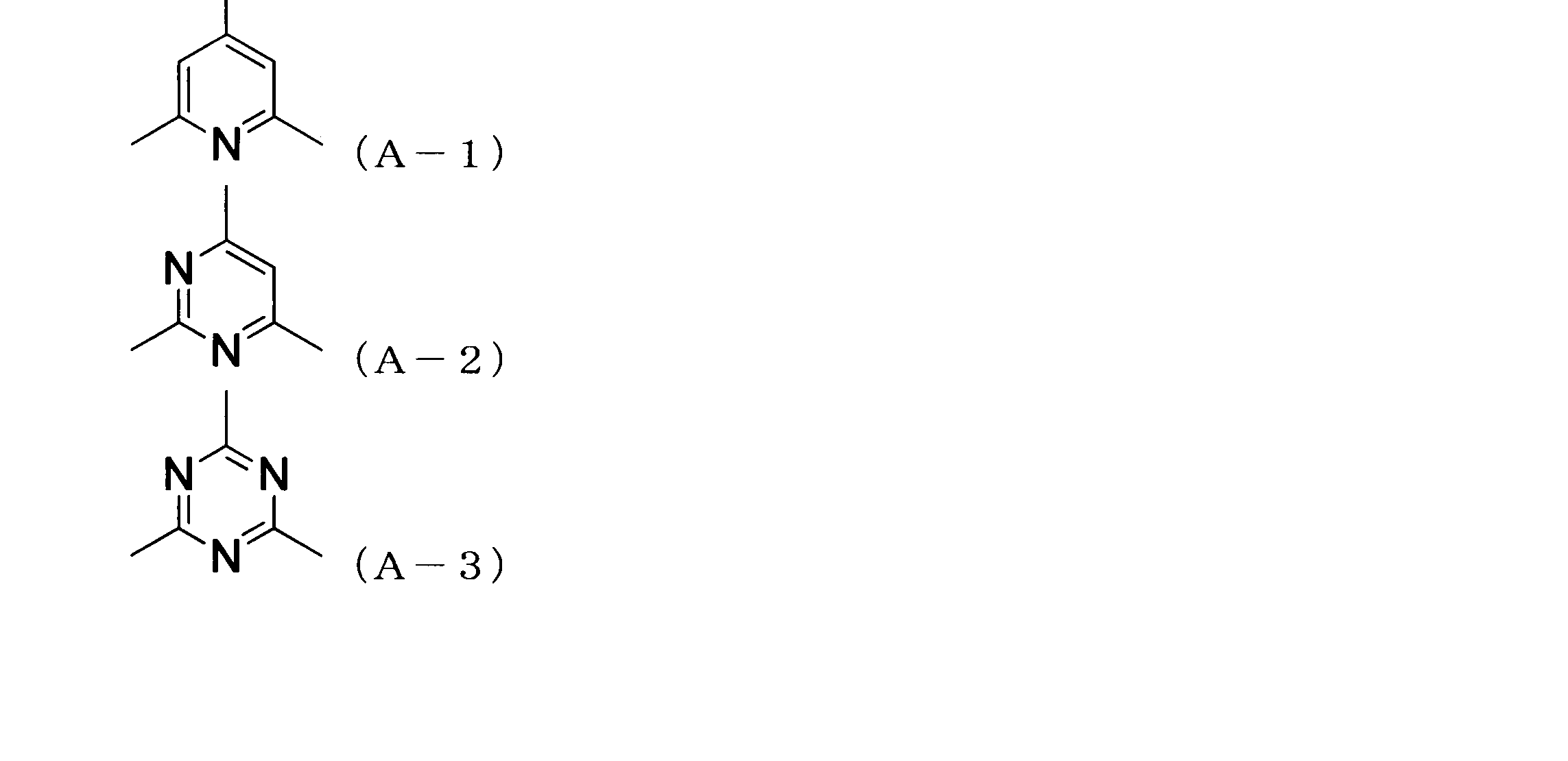

(7)前記一般式(A)で表される化合物が、前記一般式(A-4)、(A-5)及び(A-6)からなる群から選ばれるいずれか2種類のみで表される、上記(5)記載の有機電界発光素子用組成物。
(8)前記一般式(A)で表される化合物が、前記一般式(A-4)、(A-5)及び(A-6)からなる群から選ばれるいずれか1種類のみで表される、上記(5)記載の有機電界発光素子用組成物。
(9)前記化合物群αに含まれる化合物が、いずれも下記一般式(B)で表される化合物である、上記(1)~(4)のいずれか一項に記載の有機電界発光素子用組成物。
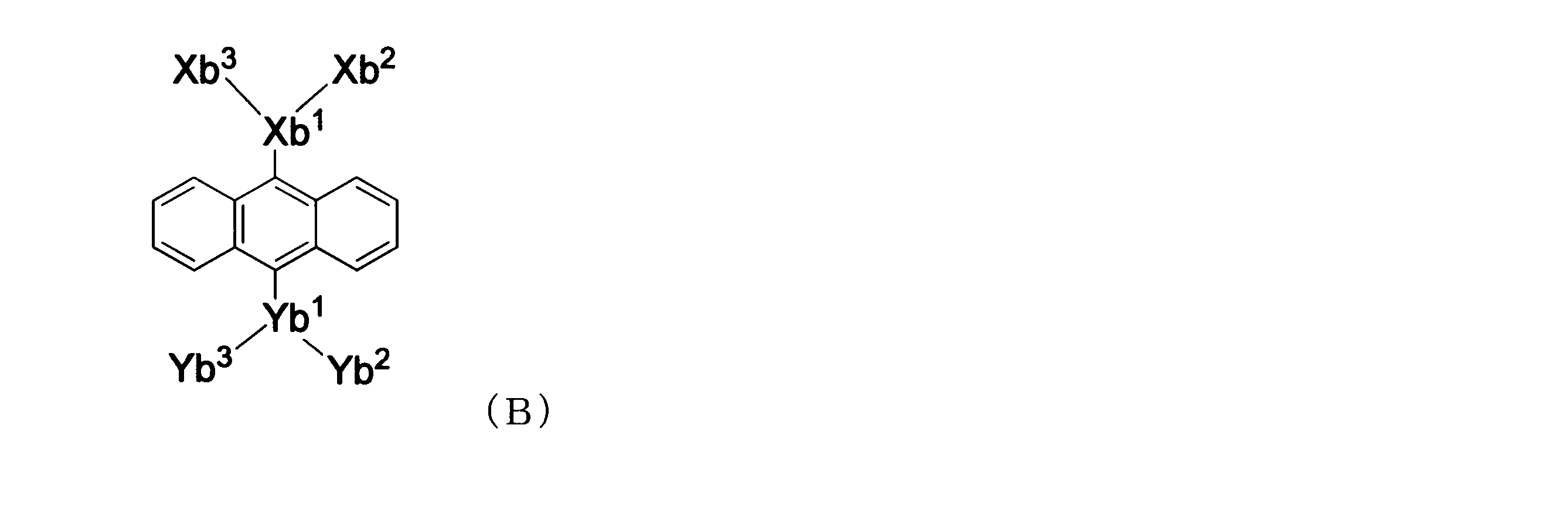
(10)前記化合物群αに含まれる材料が、いずれも下記一般式(C)で表される化合物である、上記(1)~(4)のいずれか一項に記載の有機電界発光素子用組成物。

(11)前記化合物群αに含まれる化合物が、いずれも下記一般式(D)で表される化合物である、上記(1)~(4)のいずれか一項に記載の有機電界発光素子用組成物。
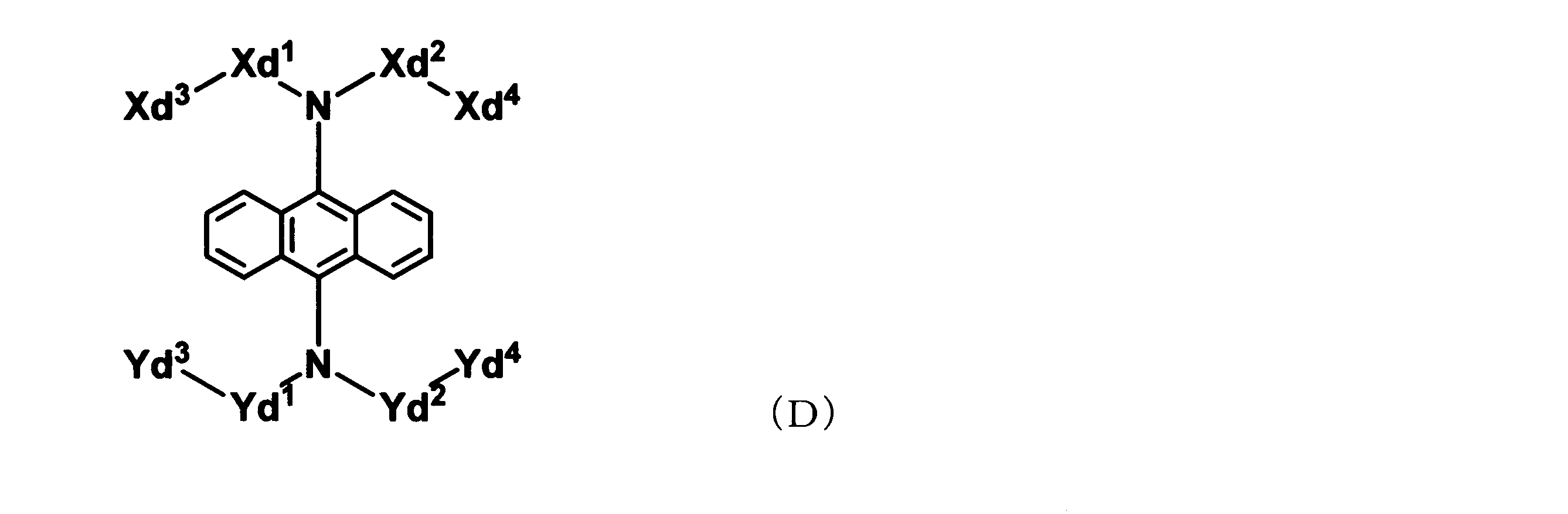
(12)前記化合物群αに含まれる化合物が、いずれも下記一般式(E)で表される化合物である、上記(1)~(4)のいずれか一項に記載の有機電界発光素子用組成物。
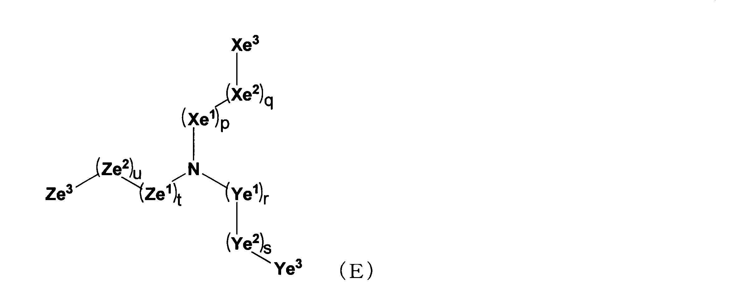
(13)前記一般式(E)で表される化合物が、下記一般式(E-1)で表わされる化合物である、上記(12)に記載の有機電界発光素子用組成物。
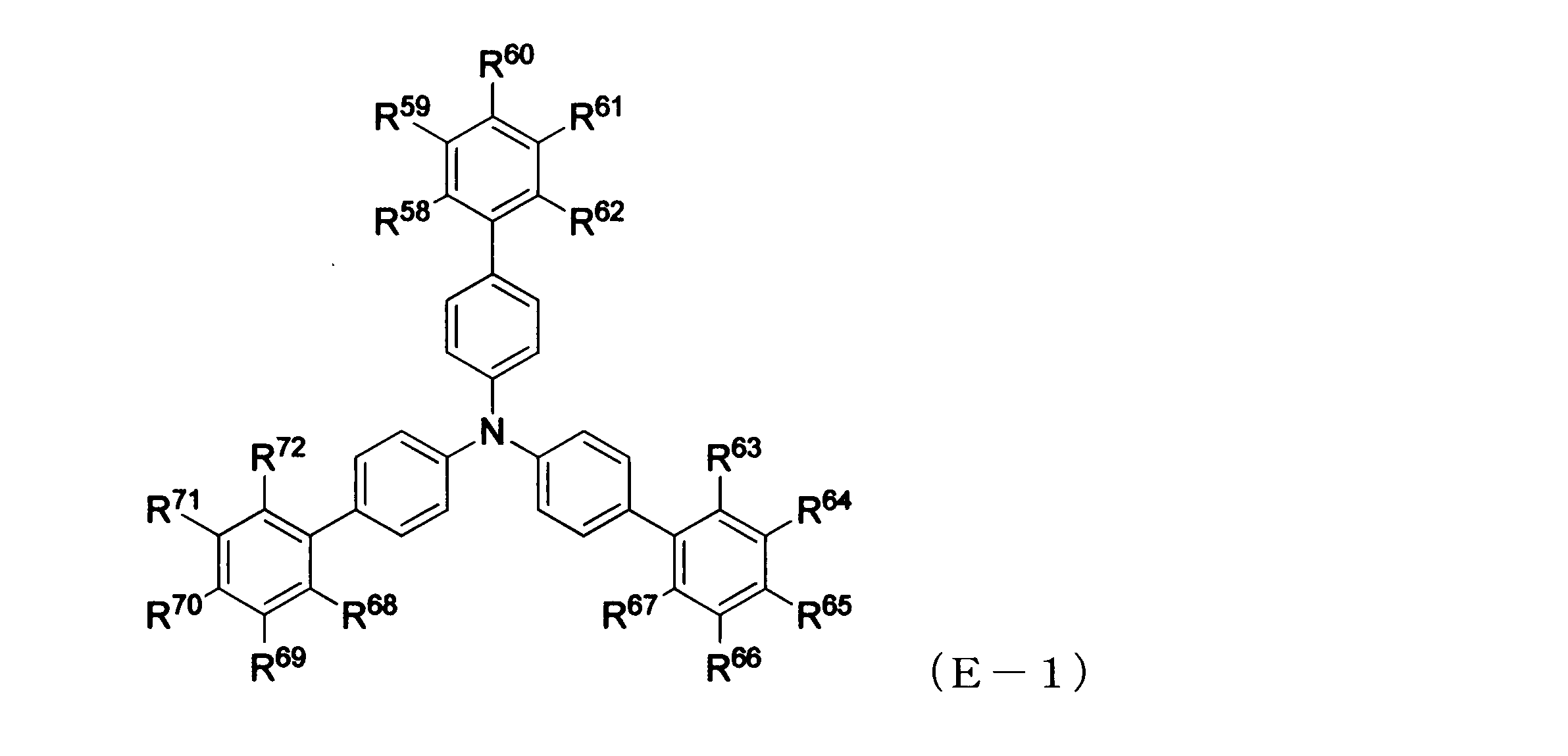
(14)陽極、陰極、及びこれらの間に少なくとも1層の有機層を有する有機電界発光素子であり、該有機層のうち少なくとも1層が、上記(1)~(13)のいずれか一項に記載の有機電界発光素子用組成物を用いて形成された層である、有機電界発光素子。
(15)上記(1)~(13)のいずれか一項に記載の有機電界発光素子用組成物を用いて形成された層が発光層である、上記(14)に記載の有機電界発光素子。
(16)上記(14)又は(15)に記載の有機電界発光素子を有する表示装置。
(17)上記(14)又は(15)に記載の有機電界発光素子を有する照明装置。
また、該組成物を用いることにより、均一な層を形成することができ、長寿命で、駆動電圧が低く、且つ発光効率の高い有機電界発光素子を提供することができる。
さらに本発明の有機電界発光素子は、面発光体としての特徴を生かした照明装置や白色光源(例えば、複写機の光源、液晶ディスプレイや計器類のバックライト光源、カラーフィルター表示装置)、表示板、及び標識灯への応用も考えられ、その技術的価値は極めて高い。
なお、本発明において「芳香環基」とは、炭化水素芳香環基及び複素芳香環基の双方を意味する。
本発明において、「(ヘテロ)アリール」とは、炭化水素芳香環及び複素芳香環のいずれも含むものとする。本発明において、「置換基を有していてもよい」とは、置換基を1又は2以上有していてもよいことを意味する。
本発明の有機電界発光素子用組成物は、有機電界発光素子用化合物群αおよび溶剤を含有する。前記化合物群αは、複数の芳香環基が連結した構造を有する、分子量3000以下である、少なくとも2種以上の化合物から構成される。この化合物群αのうち、最も芳香環基の数が少ない化合物をα1、他の化合物をαn(nは、2以上の任意の整数)とする。化合物α1と化合物αnの共通する部分構造のうち、最も芳香環基の数が多い構造を基本骨格とした場合、化合物α1の構造は、基本骨格と60%以上一致する。さらに、化合物群αを構成する各々の化合物はそれぞれ1重量%以上混合されていることを特徴とする。
下記(例1)の場合、まず、2つの化合物を構成する芳香環基の数を比較すると、芳香環基の数がより少ない化合物1が「化合物α1」に該当し、化合物2は「化合物α2」とすることができる。次に、化合物1と化合物2の構造式を比較すると、共通する部分構造のうち、最も芳香環基の数が多い構造は、化合物1そのものである(化合物1をなす環a~dが、化合物2の環e~hと一致)ため、基本骨格は化合物α1そのものとなる。したがって、化合物α1と化合物α2との基本骨格は、化合物α1と100%一致していることになる。
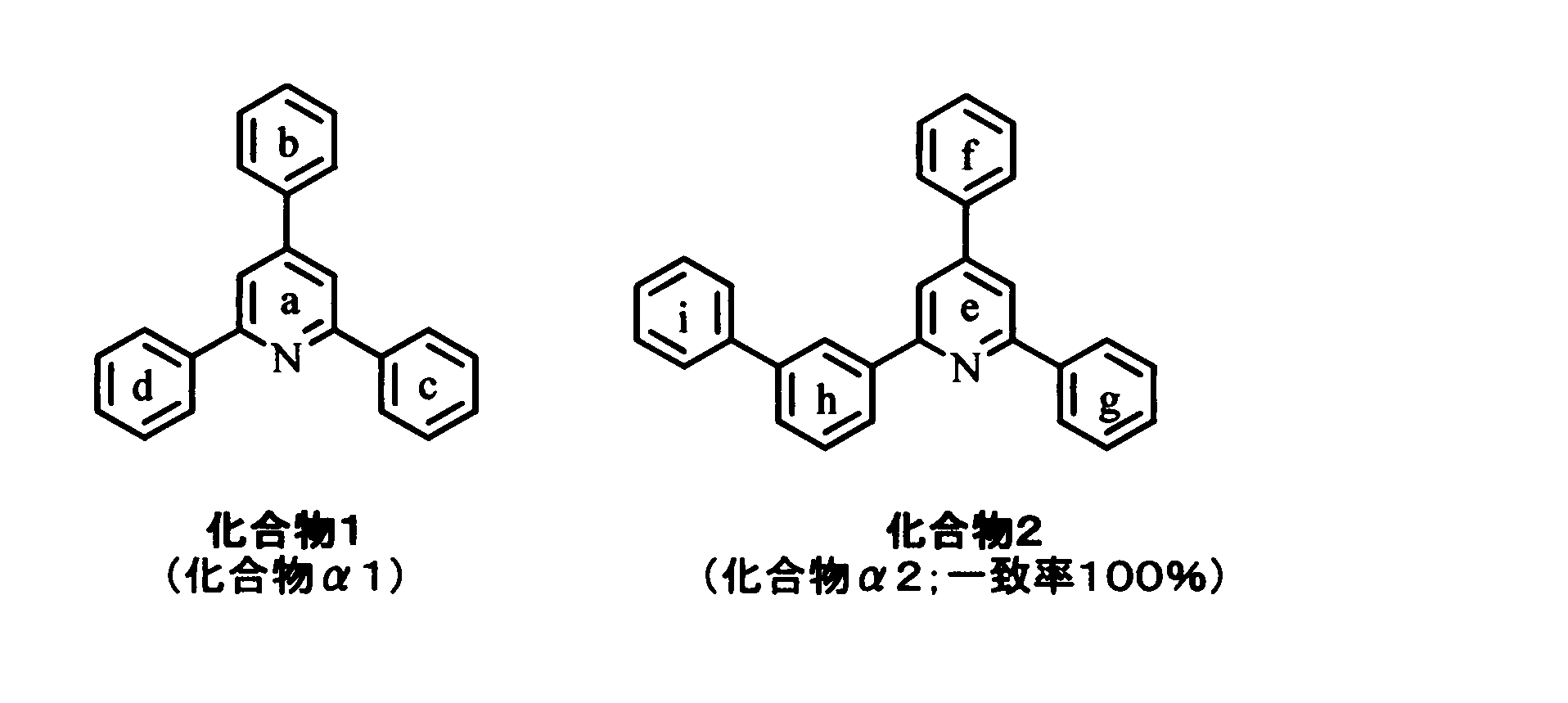
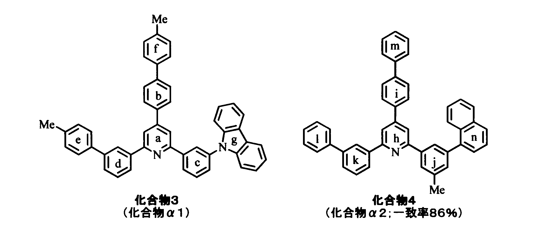
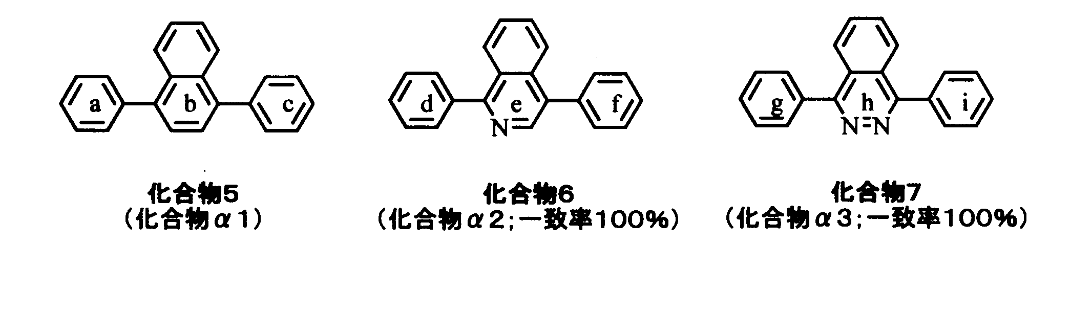
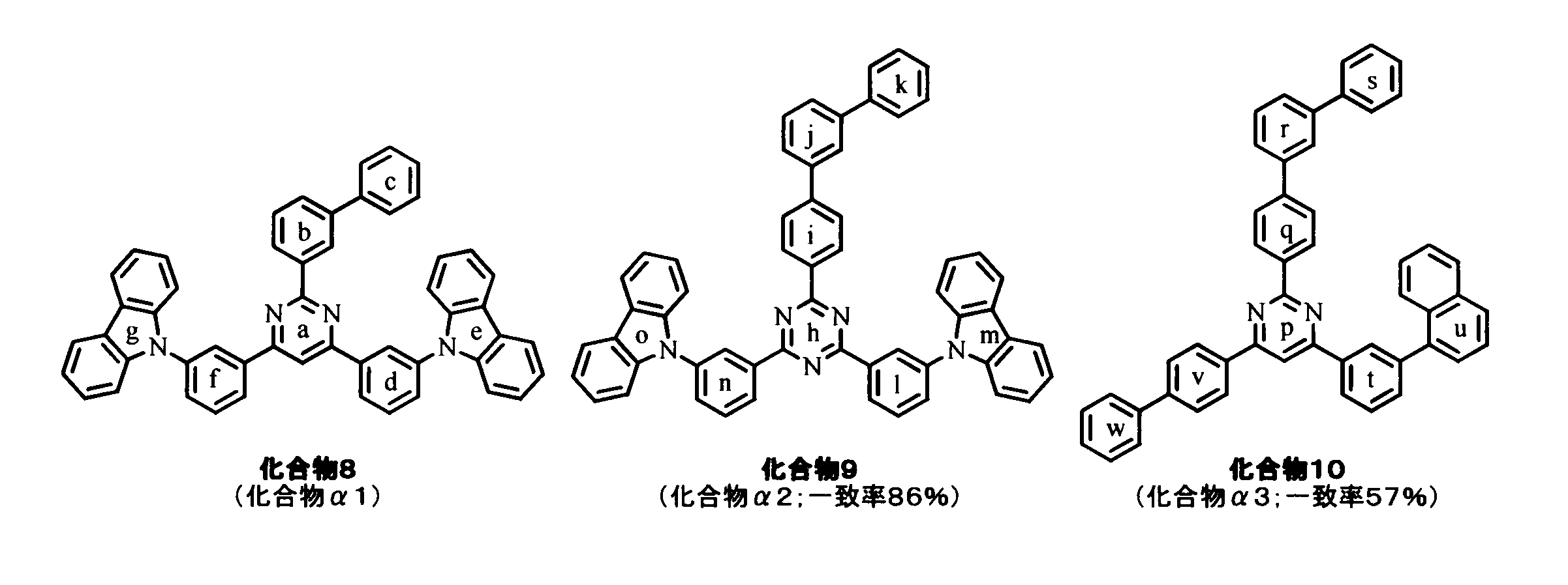
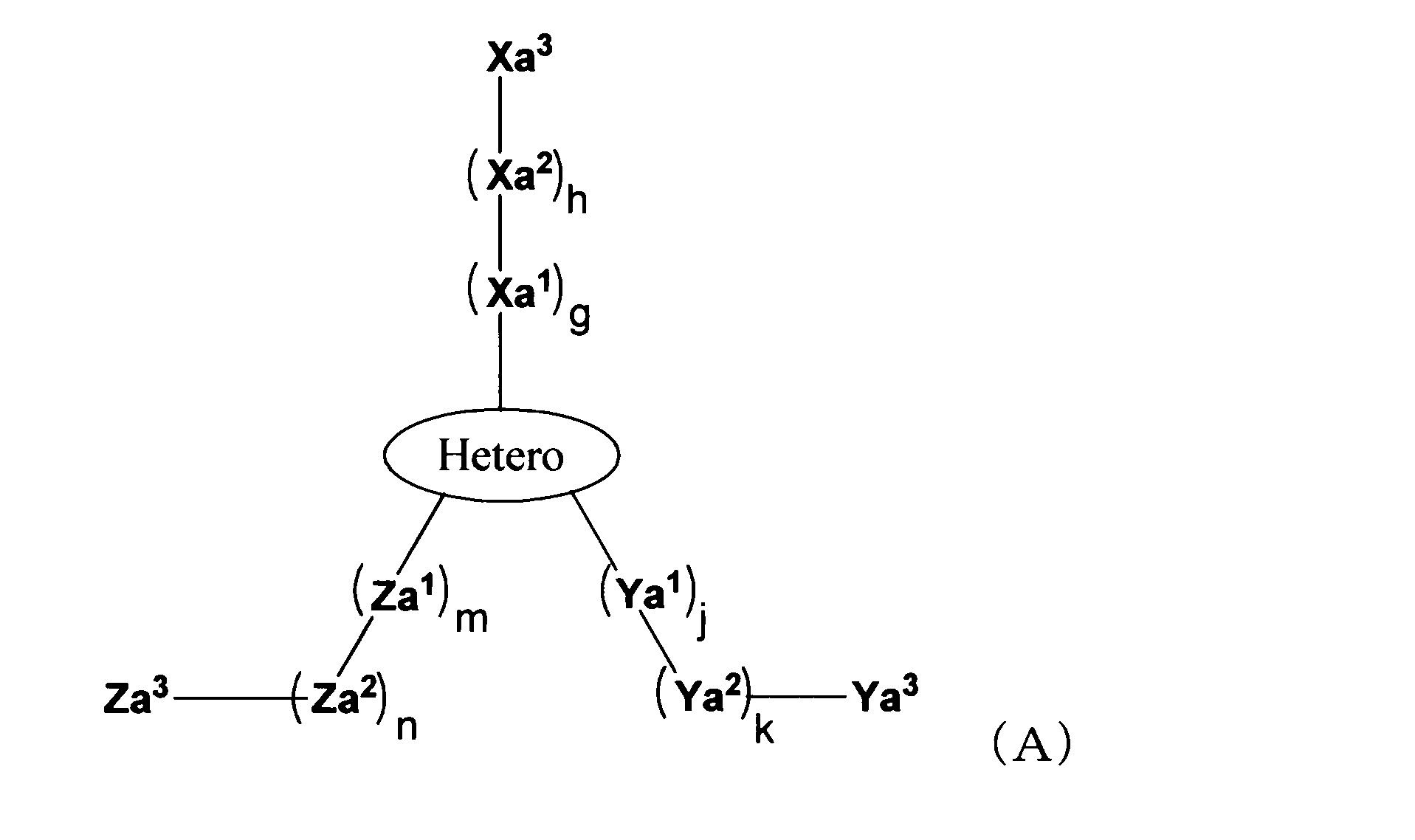


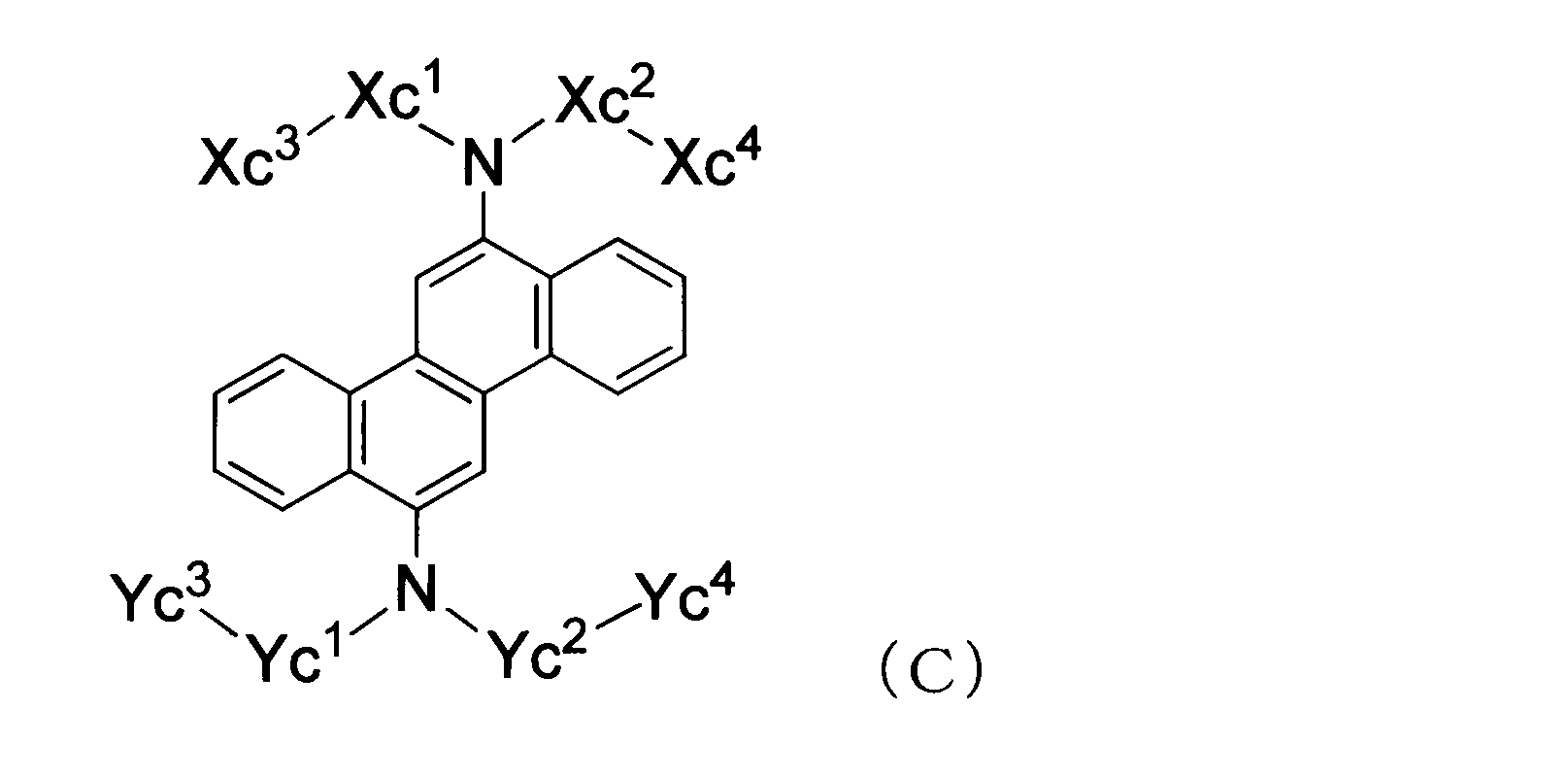


上記一般式(B)におけるXb1及びYb1、
上記一般式(C)におけるXc1、Xc2、Yc1及びYc2、
上記一般式(D)におけるXd1、Xd2、Yd1及びYd2、並びに
上記一般式(E)におけるXe1、Xe2、Ye1、Ye2、Ze1及びZe2
は、いずれも各々独立に、置換基を有していてもよい炭素数6~30の炭化水素芳香環基、又は置換基を有していてもよい炭素数3~30の複素芳香環基を表す。
ここで、本発明において、遊離原子価とは、有機化学・生化学命名法(上)(改定第2版、南江堂、1992年発行)に記載のとおり、他の遊離原子価と結合を形成できるものを言う。すなわち、例えば、「1個の遊離原子価を有するベンゼン環」はフェニル基のことを言い、「2個の遊離原子価を有するベンゼン環」はフェニレン基のことを言う。
上記一般式(B)におけるXb2、Xb3、Yb2及びYb3、
上記一般式(C)におけるXc3、Xc4、Yc3及びYc4、
上記一般式(D)におけるXd3、Xd4、Yd3及びYd4、並びに
上記一般式(E)におけるXe3、Ye3及びZe3
は、いずれも各々独立に、水素原子、置換基を有していてもよい炭素数6~30の炭化水素芳香環基、又は置換基を有していてもよい炭素数3~30の複素芳香環基を表す。
炭素数6~25の1価の芳香族炭化水素環基としては、フェニル基、1-ナフチル基、2-ナフチル基などのナフチル基;9-フェナンチル基、3-フェナンチル基などのフェナンチル基;1-アントリル基、2-アントリル基、9-アントリル基などのアントリル基;1-ナフタセニル基、2-ナフタセニル基などのナフタセニル基;1-クリセニル基、2-クリセニル基、3-クリセニル基、4-クリセニル基、5-クリセニル基、6-クリセニル基などのクリセニル基;1-ピレニル基などのピレニル基;1-トリフェニレニル基などのトリフェニレニル基;1-コロネニル基などのコロネニル基;4-ビフェニル基、3-ビフェニル基のビフェニル基;フルオランテン環を有する基;フルオレン環を有する基;アセナフテン環を有する基及びベンズピレン環等を有する置換基などが挙げられる。これらの内、有機電界発光素子の電荷輸送材料としての耐久性の点からフェニル基、2-ナフチル基及び3-ビフェニル基が好ましく、精製のし易さからフェニル基が特に好ましい。
炭素数3~20の芳香族複素環基としては、2-チエニル基などのチエニル基;2-フリル基などのフリル基;2-イミダゾリル基などのイミダゾリル基;9-カルバゾリル基などのカルバゾリル基;2-ピリジル基などのピリジル基及び1,3,5-トリアジン-2-イル基などのトリアジニル基等が挙げられる。これらの内、有機電界発光素子の電荷輸送材料としての耐久性の点から、カルバゾリル基が好ましい。
炭素数12~60のジアリールアミノ基としては、ジフェニルアミノ基、N-1-ナフチル-N-フェニルアミノ基、N-2-ナフチル-N-フェニルアミノ基、N-9-フェナントリル-N-フェニルアミノ基、N-(ビフェニル‐4‐イル)-N-フェニルアミノ基、ビス(ビフェニル-4-イル)アミノ基等が挙げられる。中でもジフェニルアミノ基、N-1-ナフチル-N-フェニルアミノ基、N-2-ナフチル-N-フェニルアミノ基が好ましく、特にジフェニルアミノ基が安定性の点で好ましい。ただし、一般式(B)においては、耐久性の観点からジアリールアミノ基の置換基は有していない方が好ましい。
炭素数1~20のアルキルオキシ基としては、メトキシ基、エトキシ基、イソプロピルオキシ基、シクロヘキシルオキシ基及びオクタデシルオキシ基等が挙げられる。
炭素数3~20の(ヘテロ)アリールオキシ基としては、フェノキシ基、1-ナフチルオキシ基、9-アントラニルオキシ基等のアリールオキシ基及び2-チエニルオキシ基等のヘテロアリールオキシ基を有する置換基等が挙げられる。
炭素数1~20のアルキルチオ基としては、メチルチオ基、エチルチオ基、イソプロピルチオ基及びシクロヘキシルチオ基等が挙げられる。
炭素数3~20の(ヘテロ)アリールチオ基としては、フェニルチオ基、1-ナフチルチオ基、9-アントラニルチオ基等のアリールチオ基及び2-チエニルチオ基等のヘテロアリールチオ基等が挙げられる。
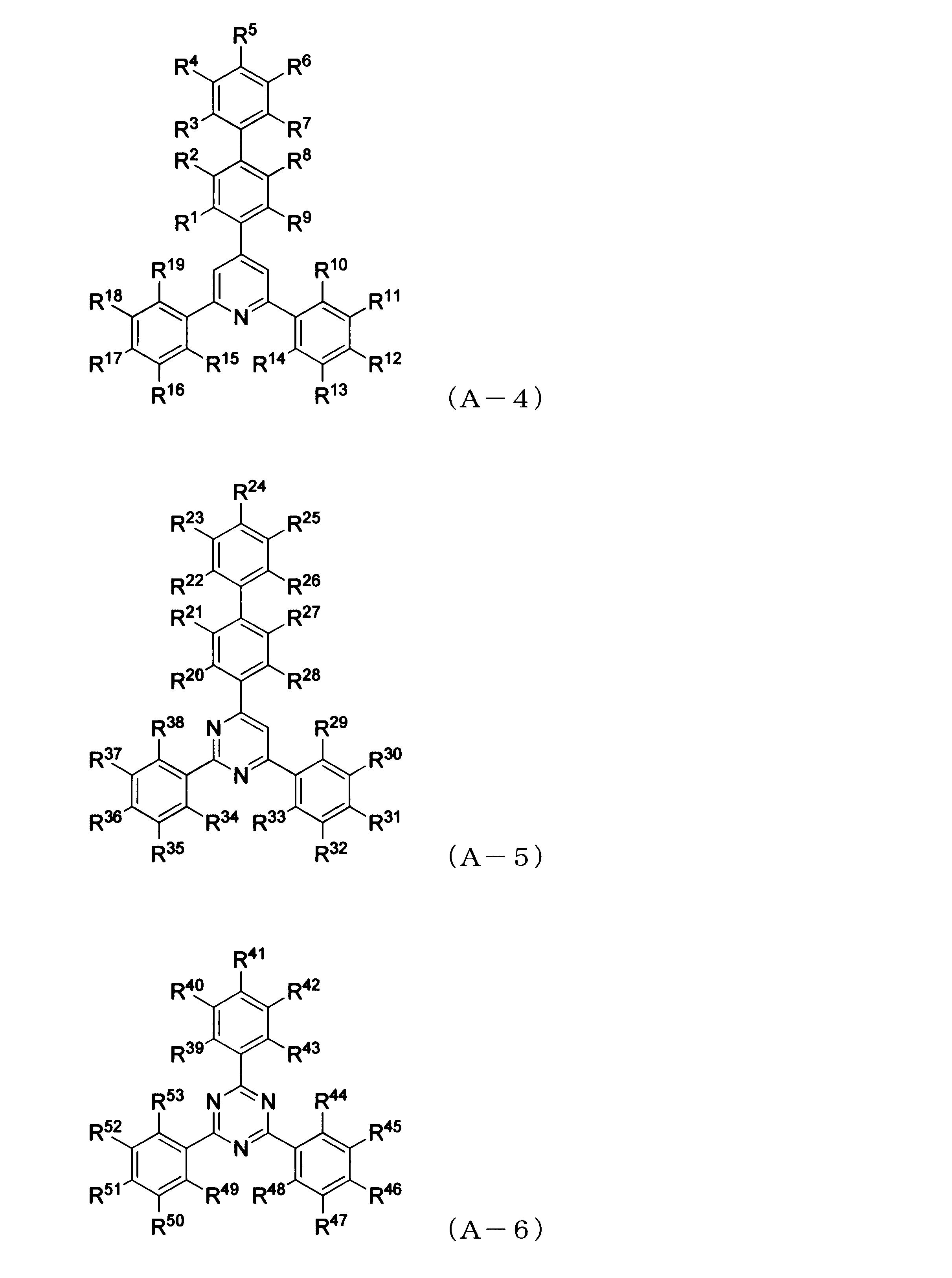
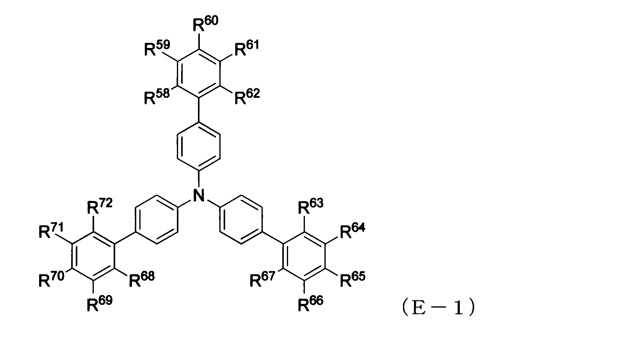
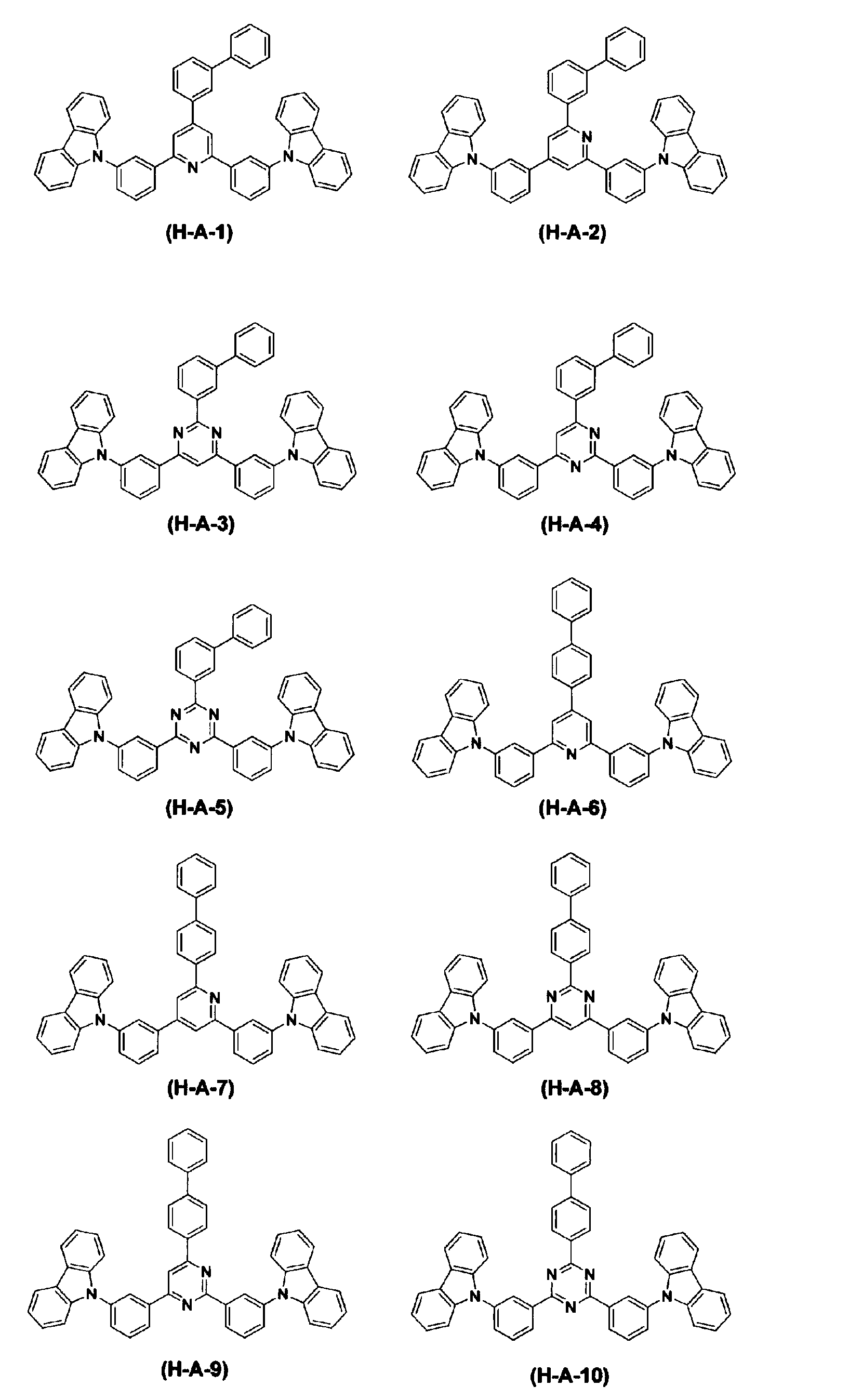
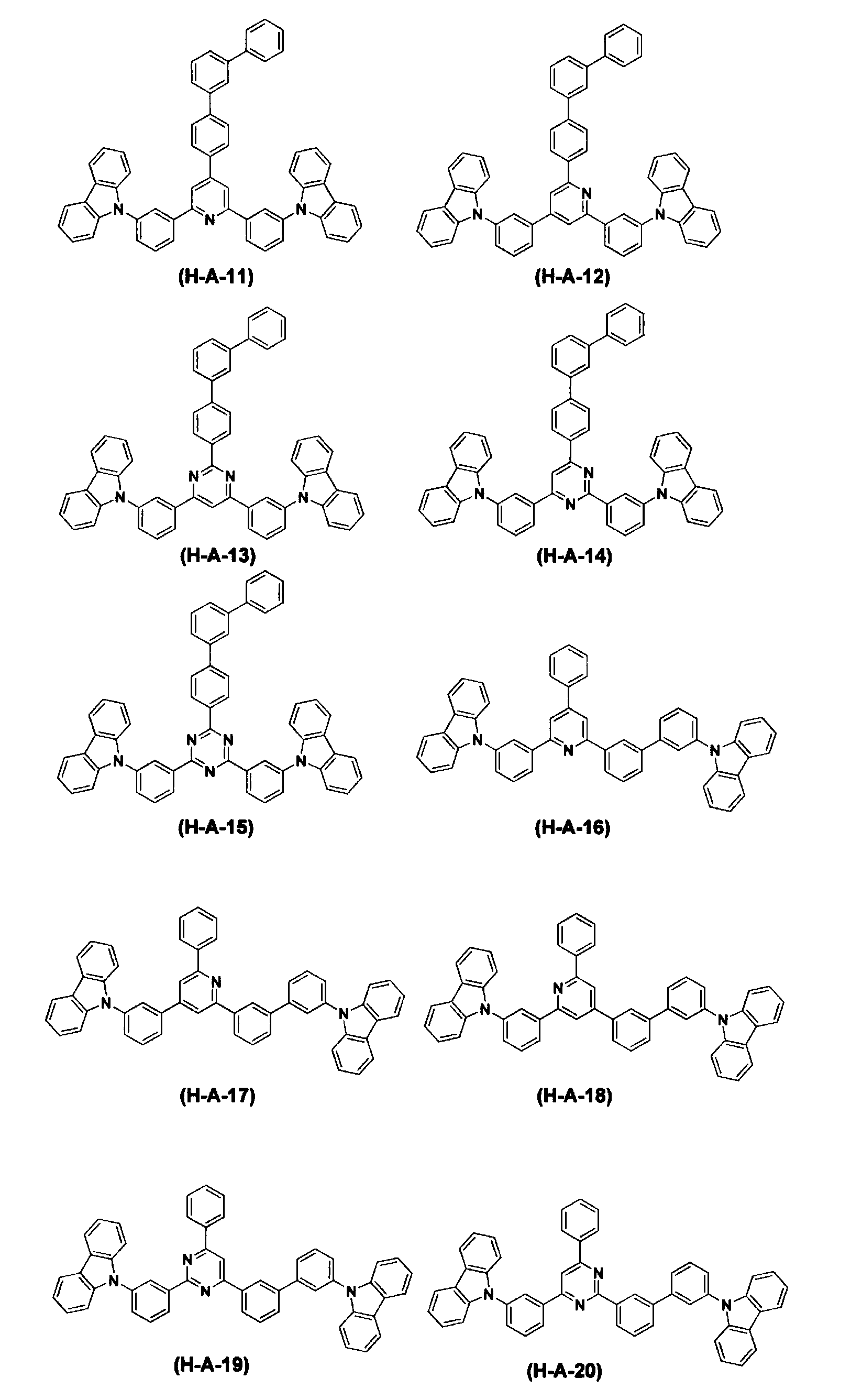
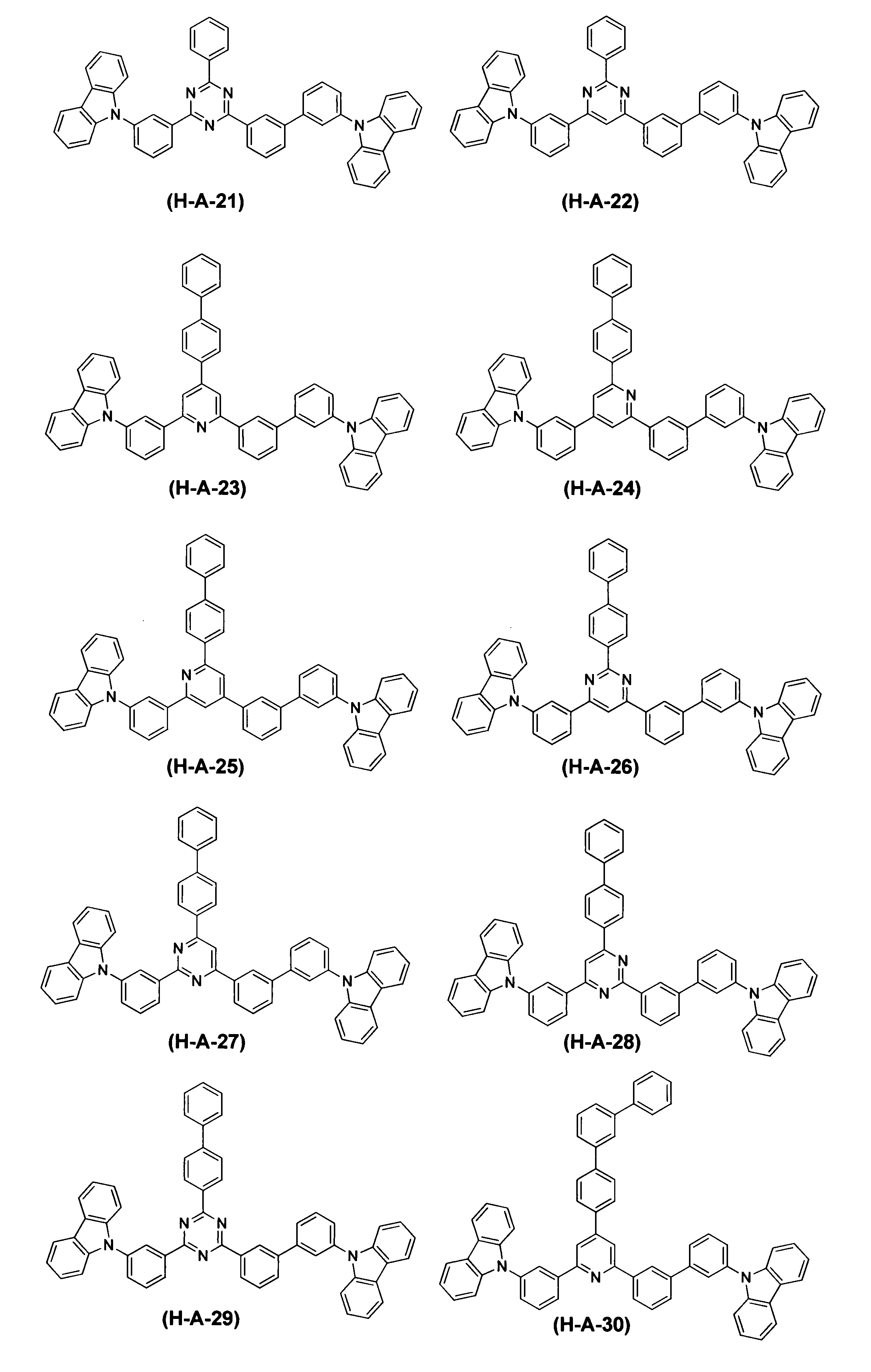
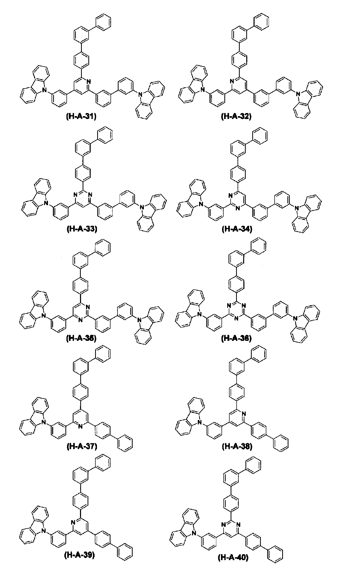
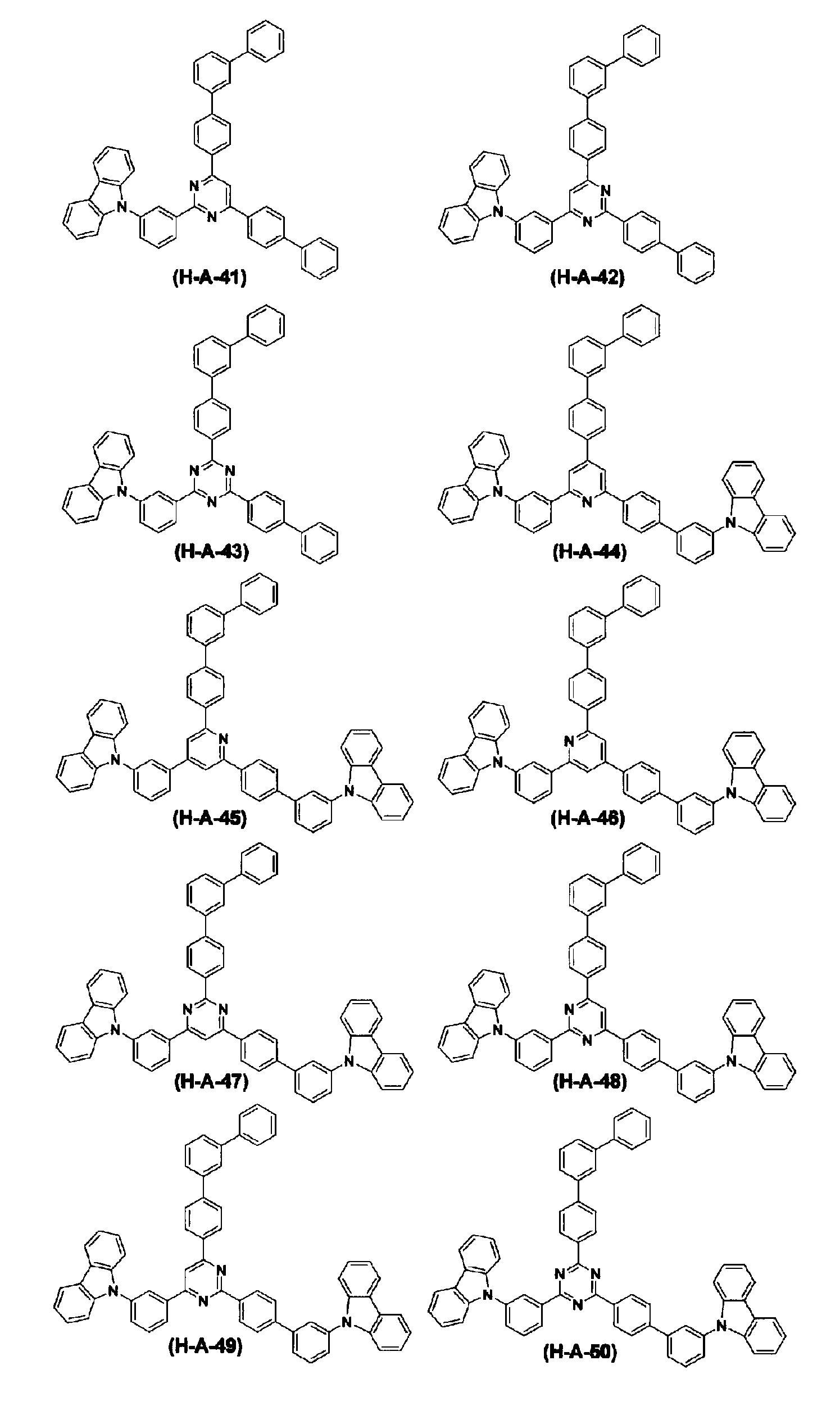

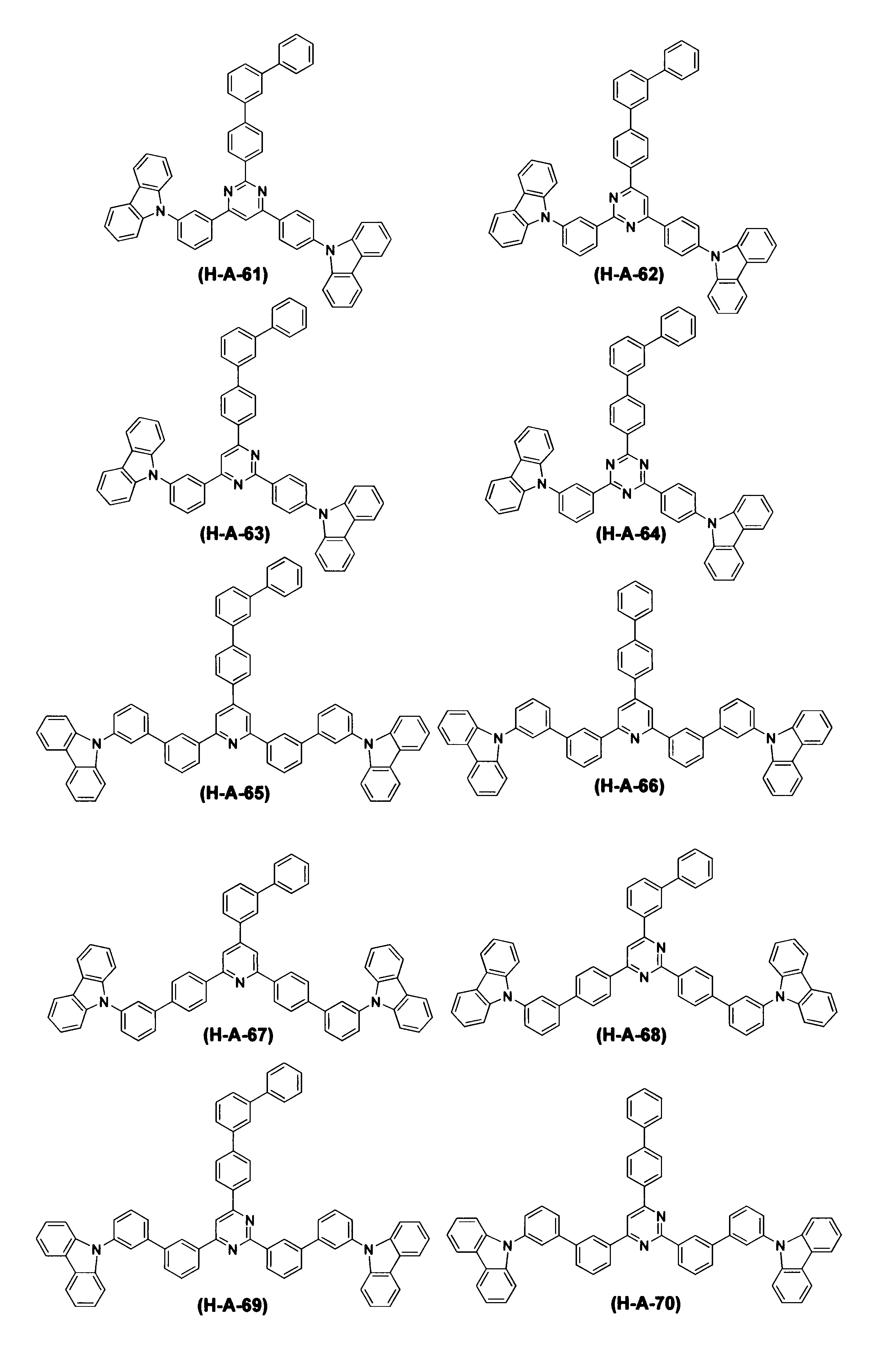
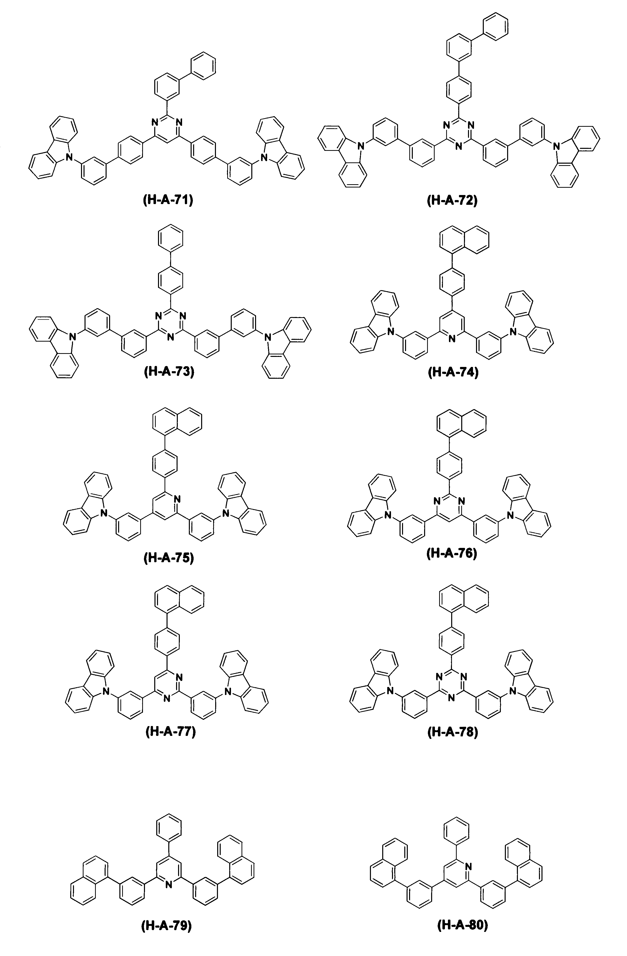
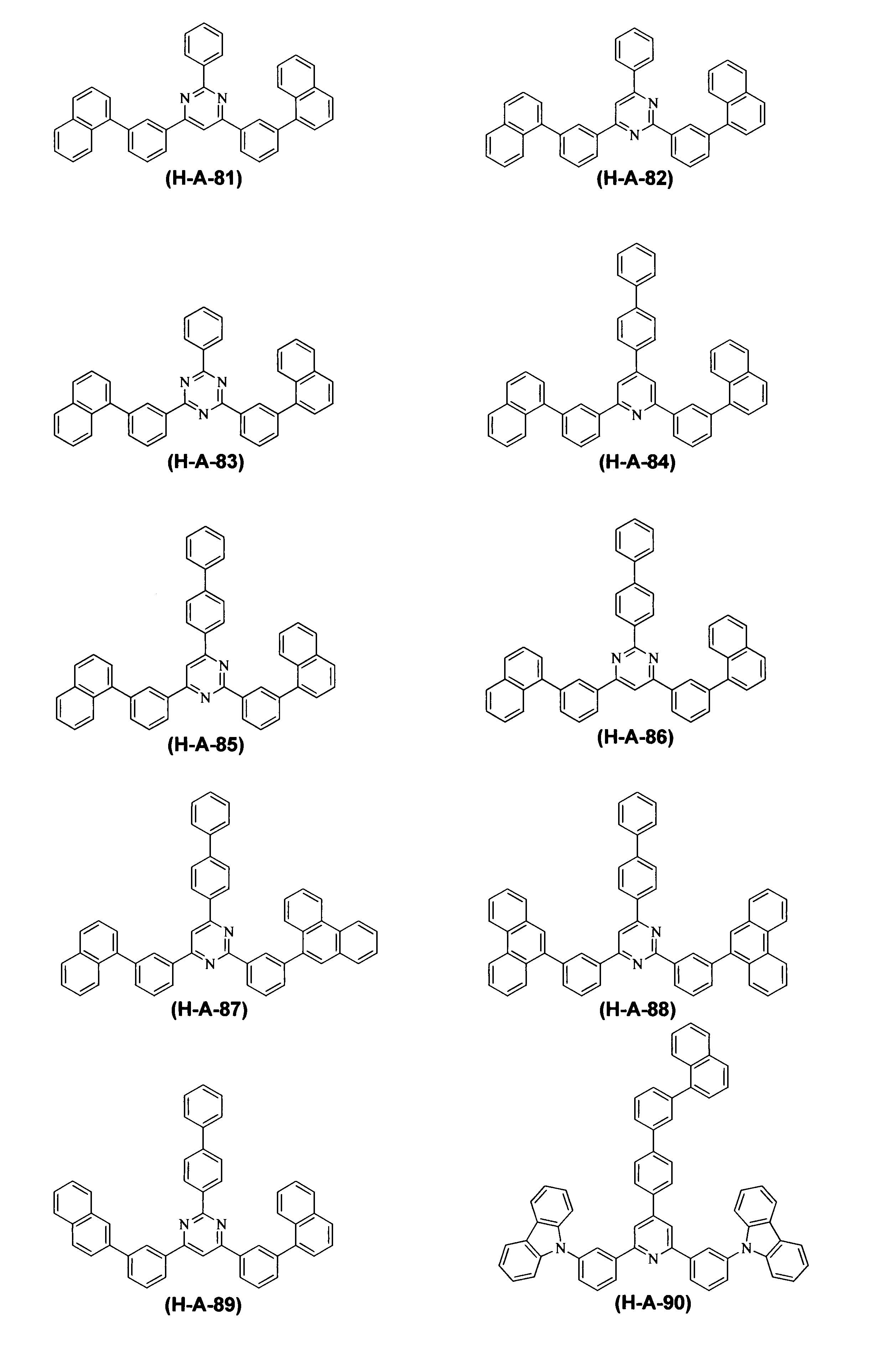

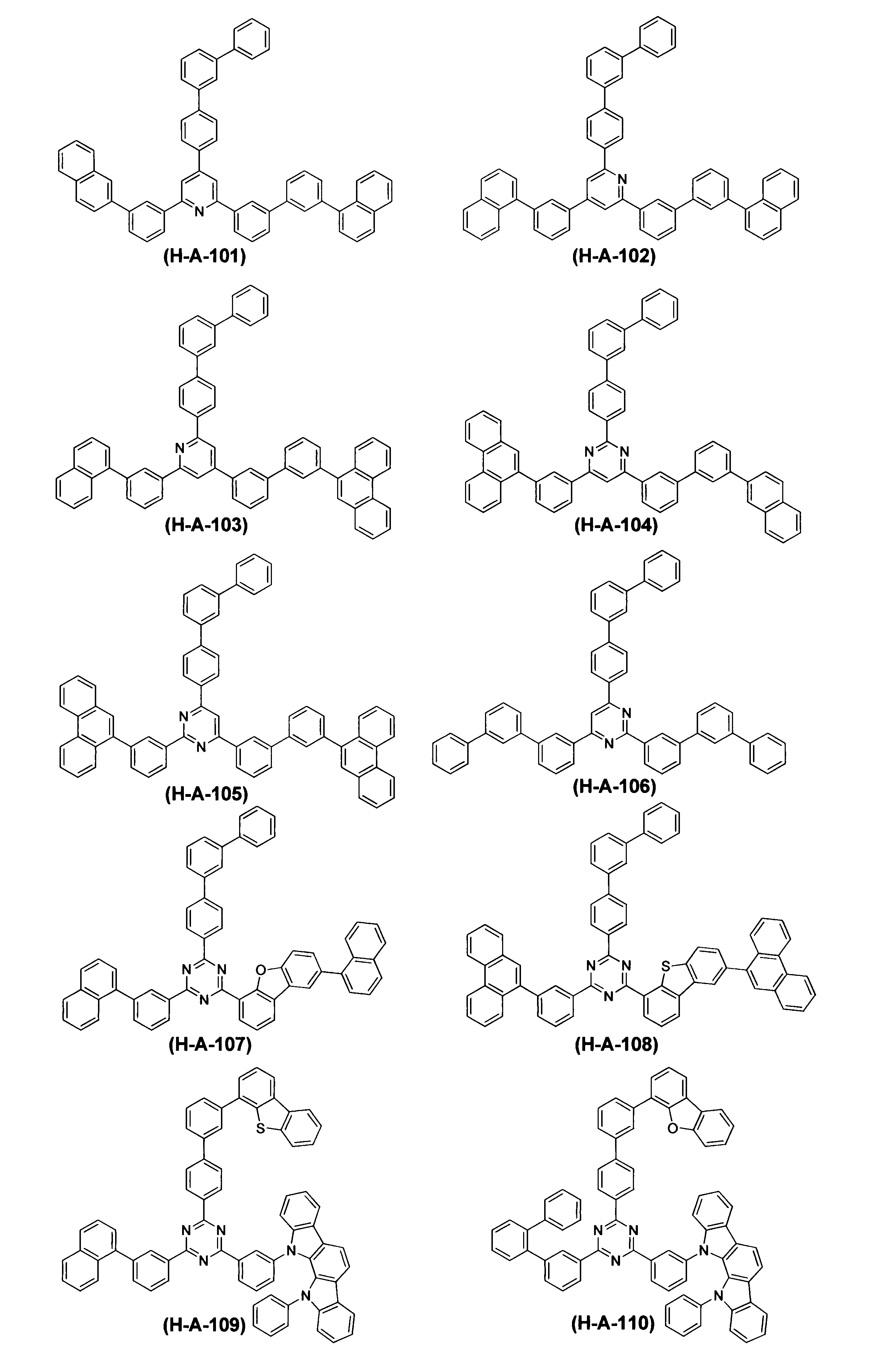

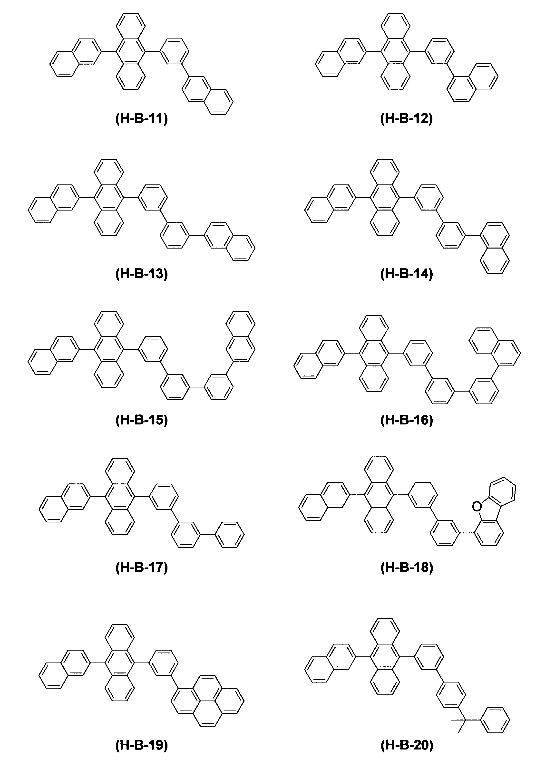
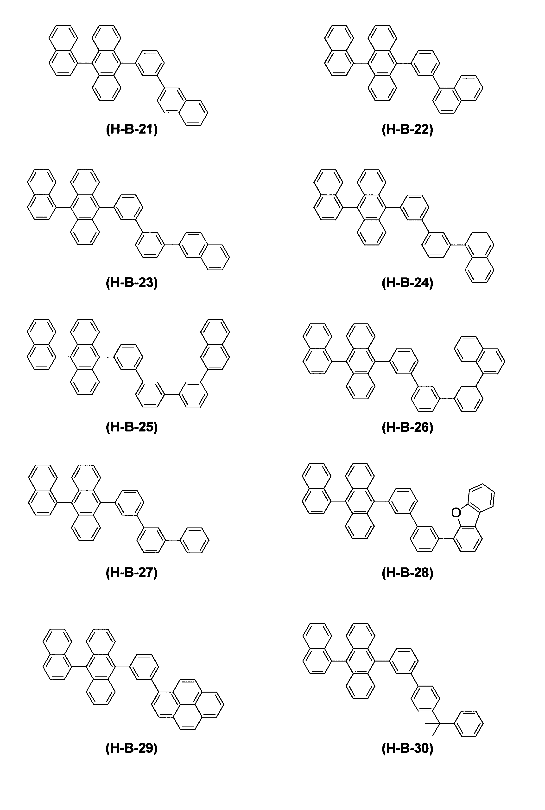


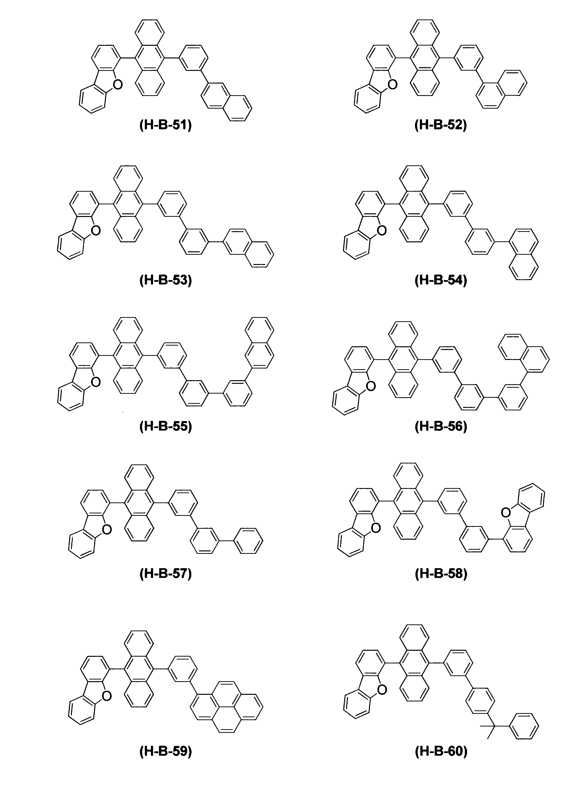
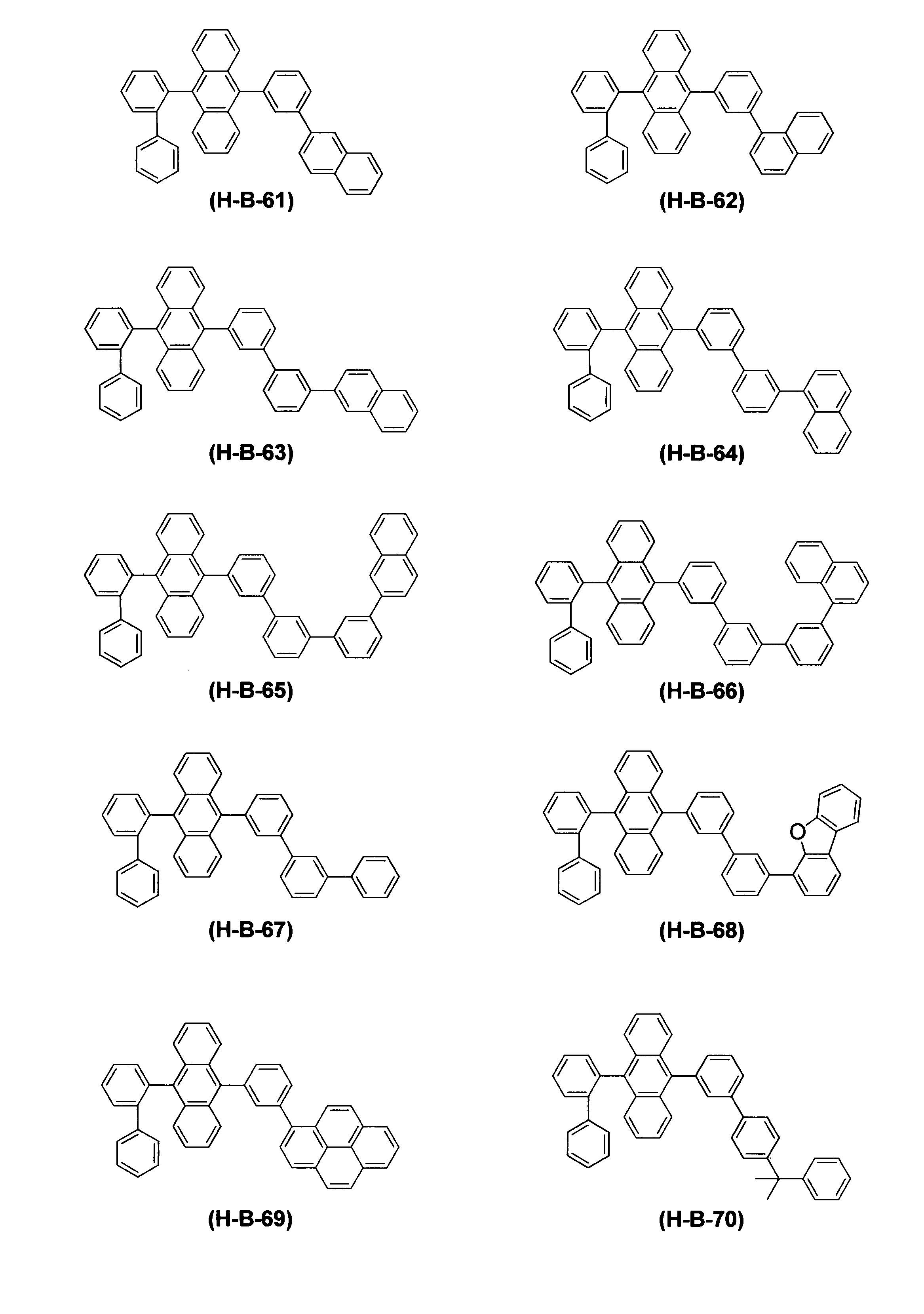


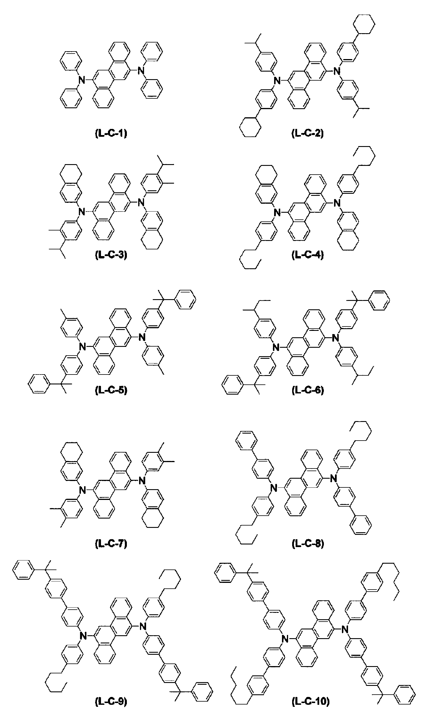

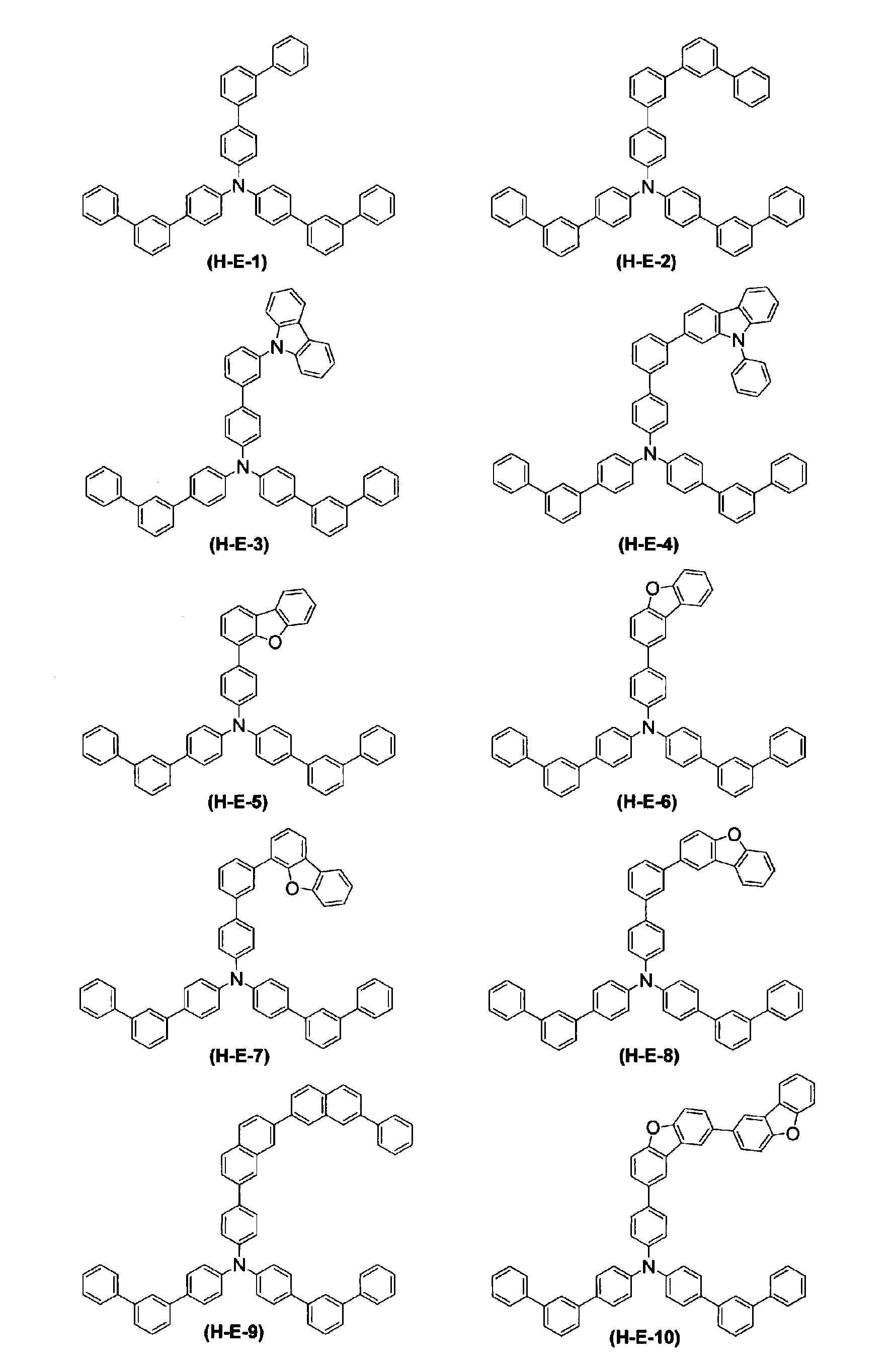
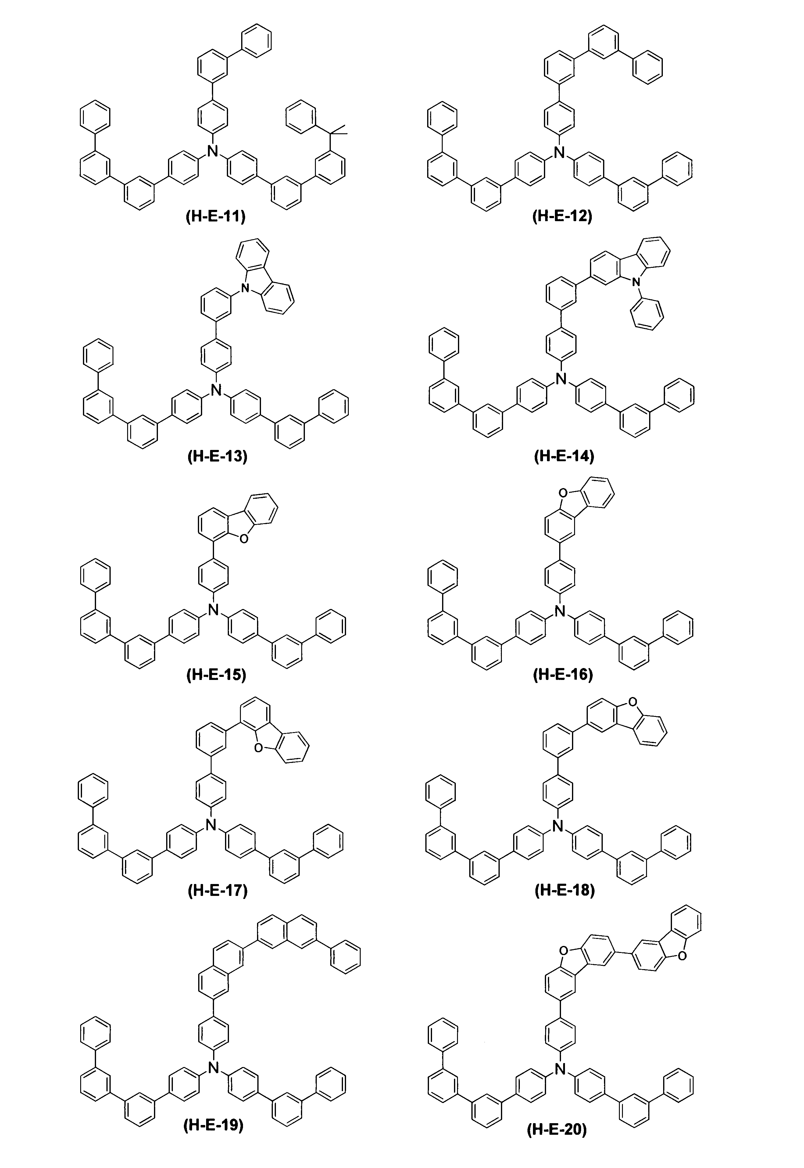
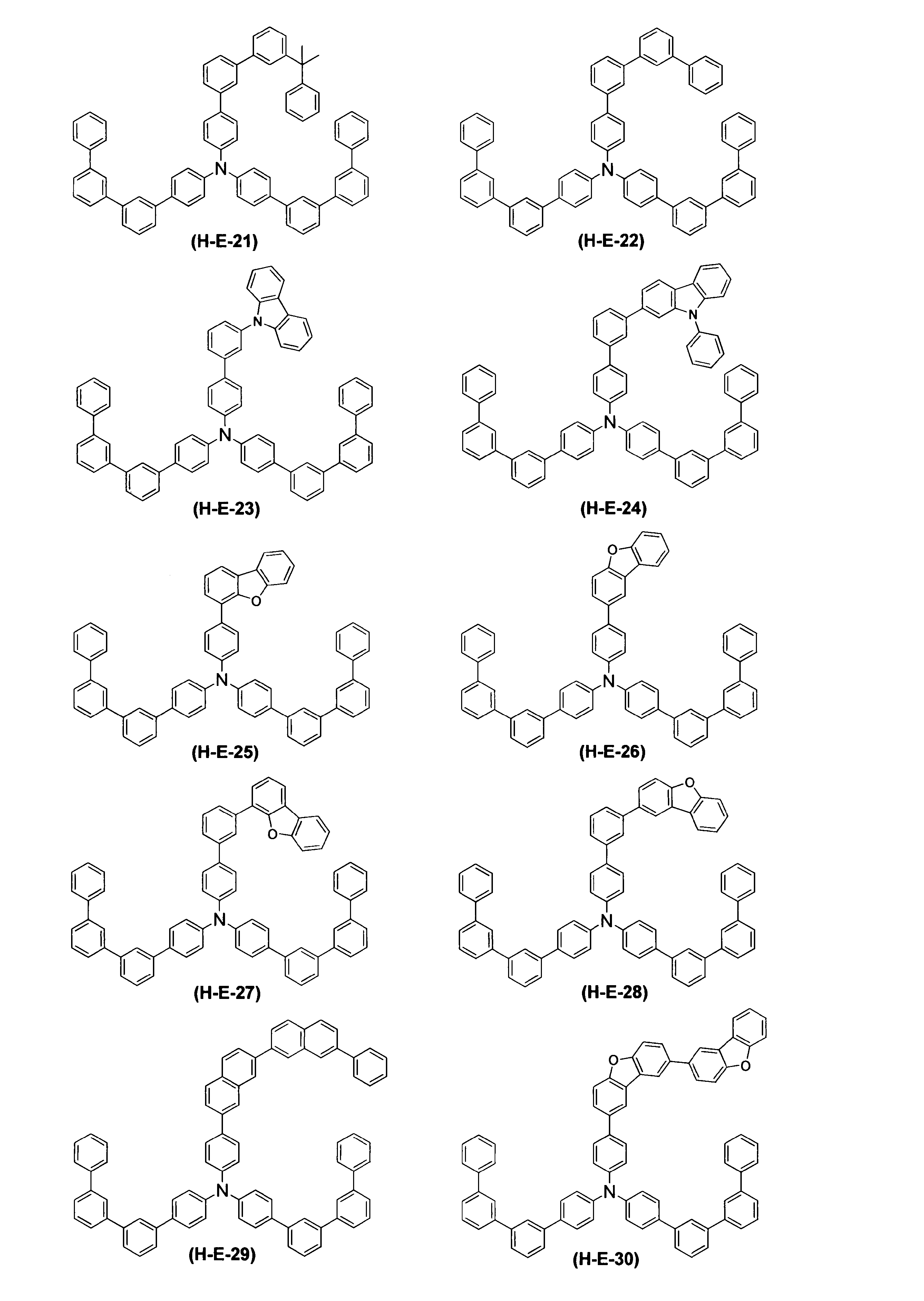
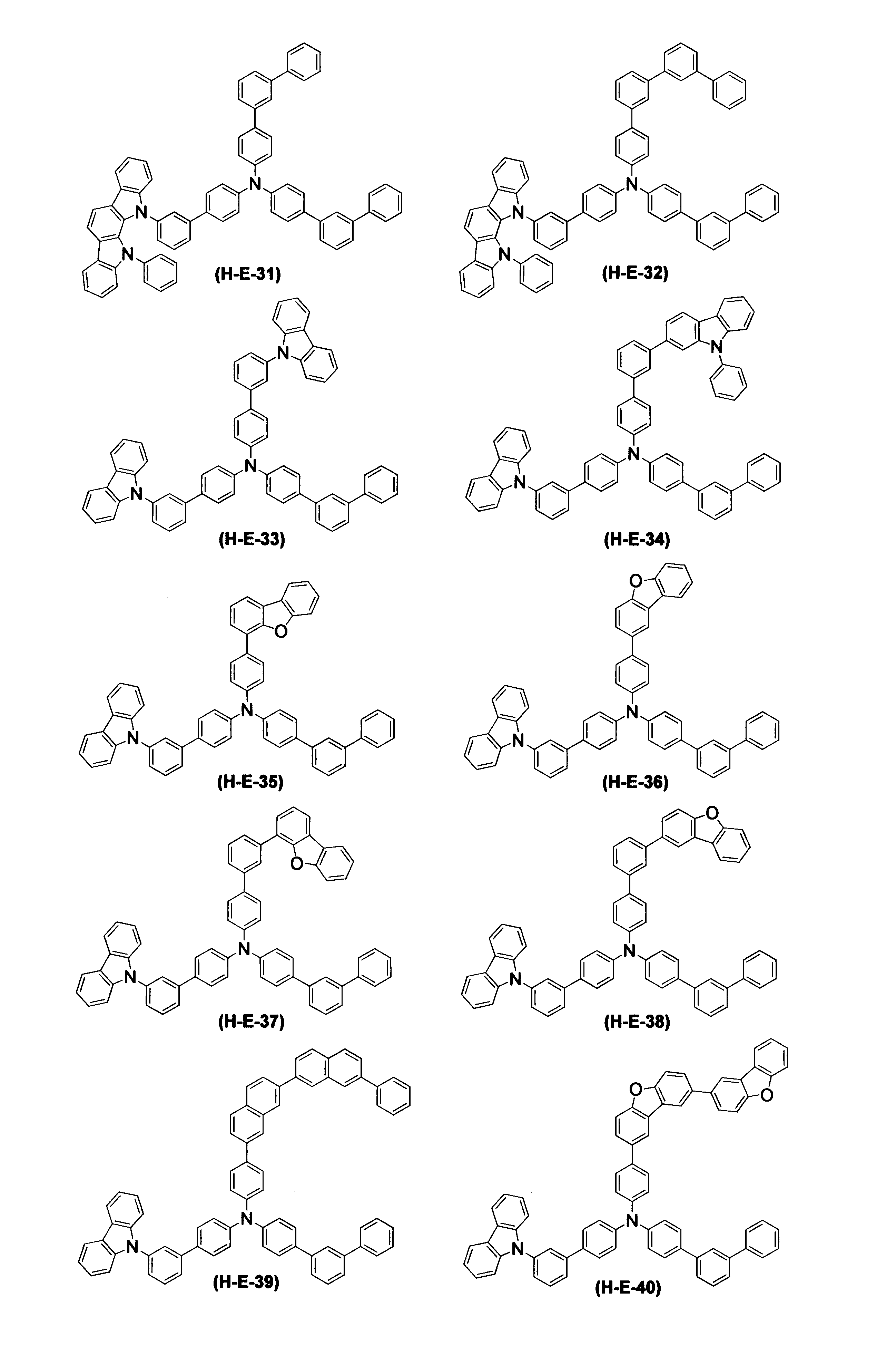

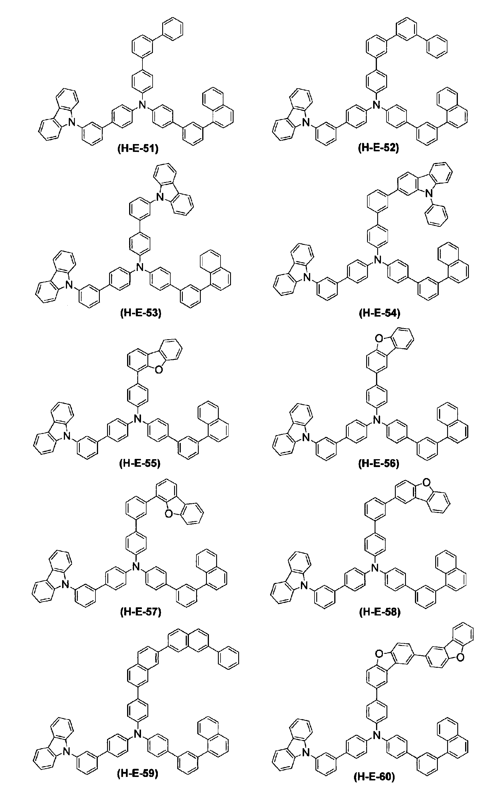
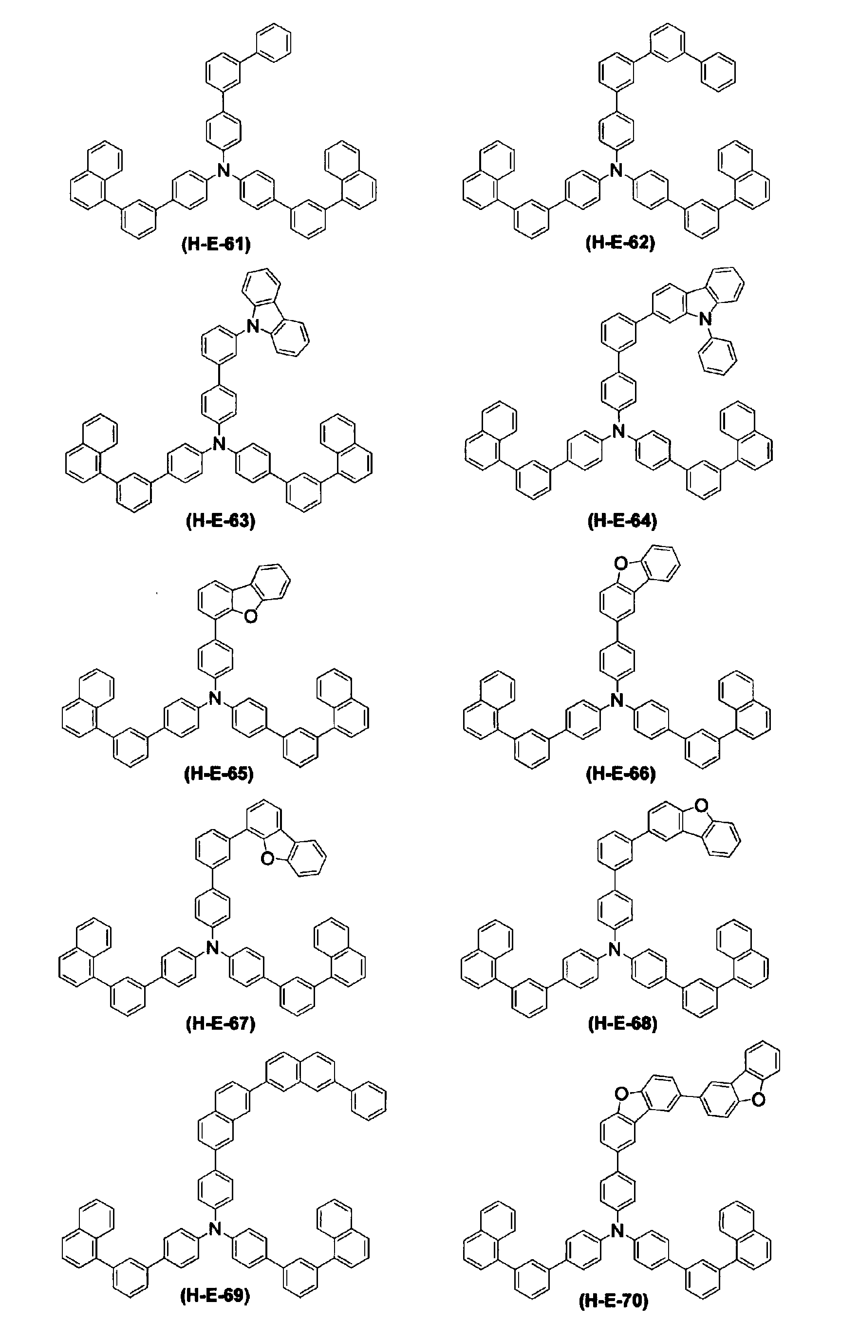
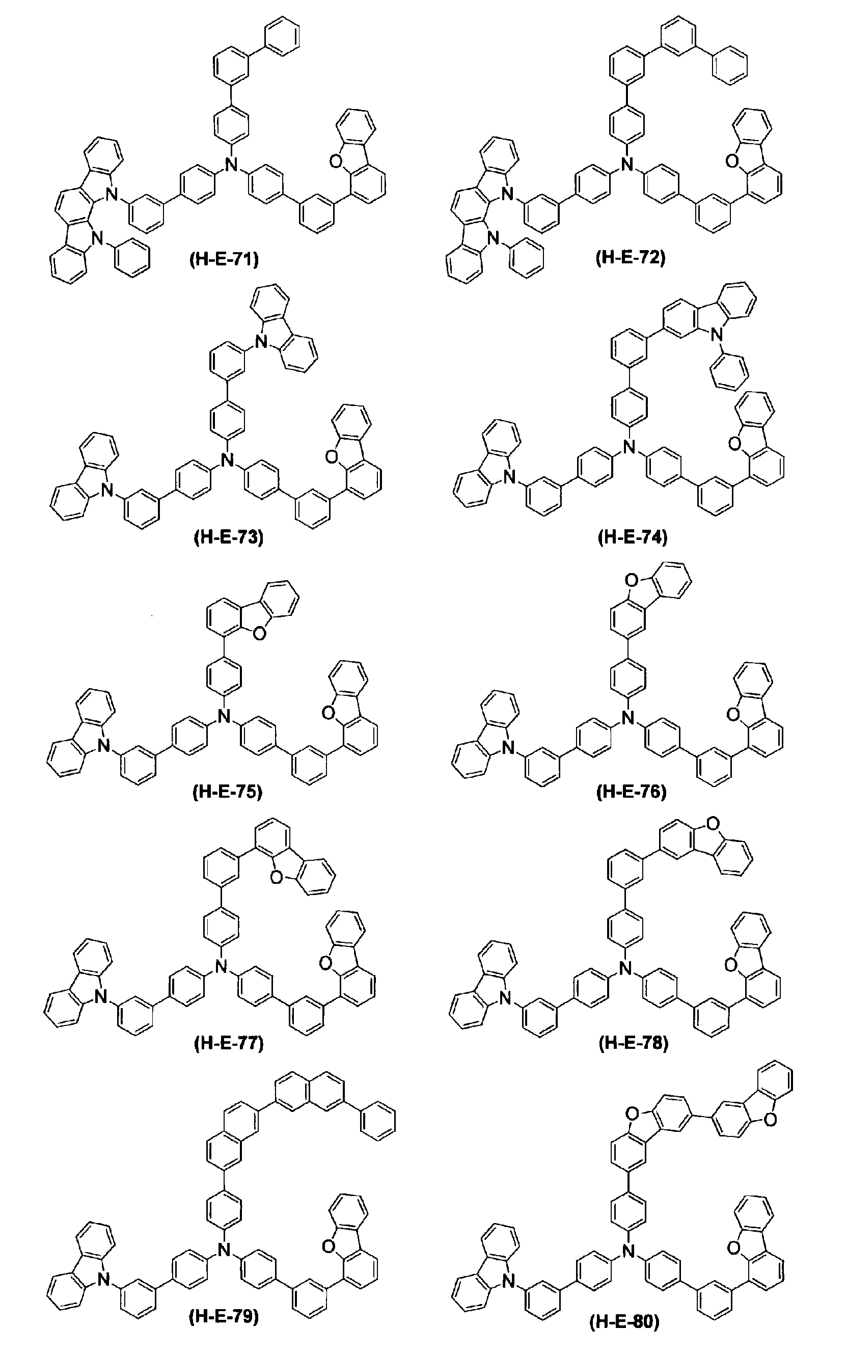
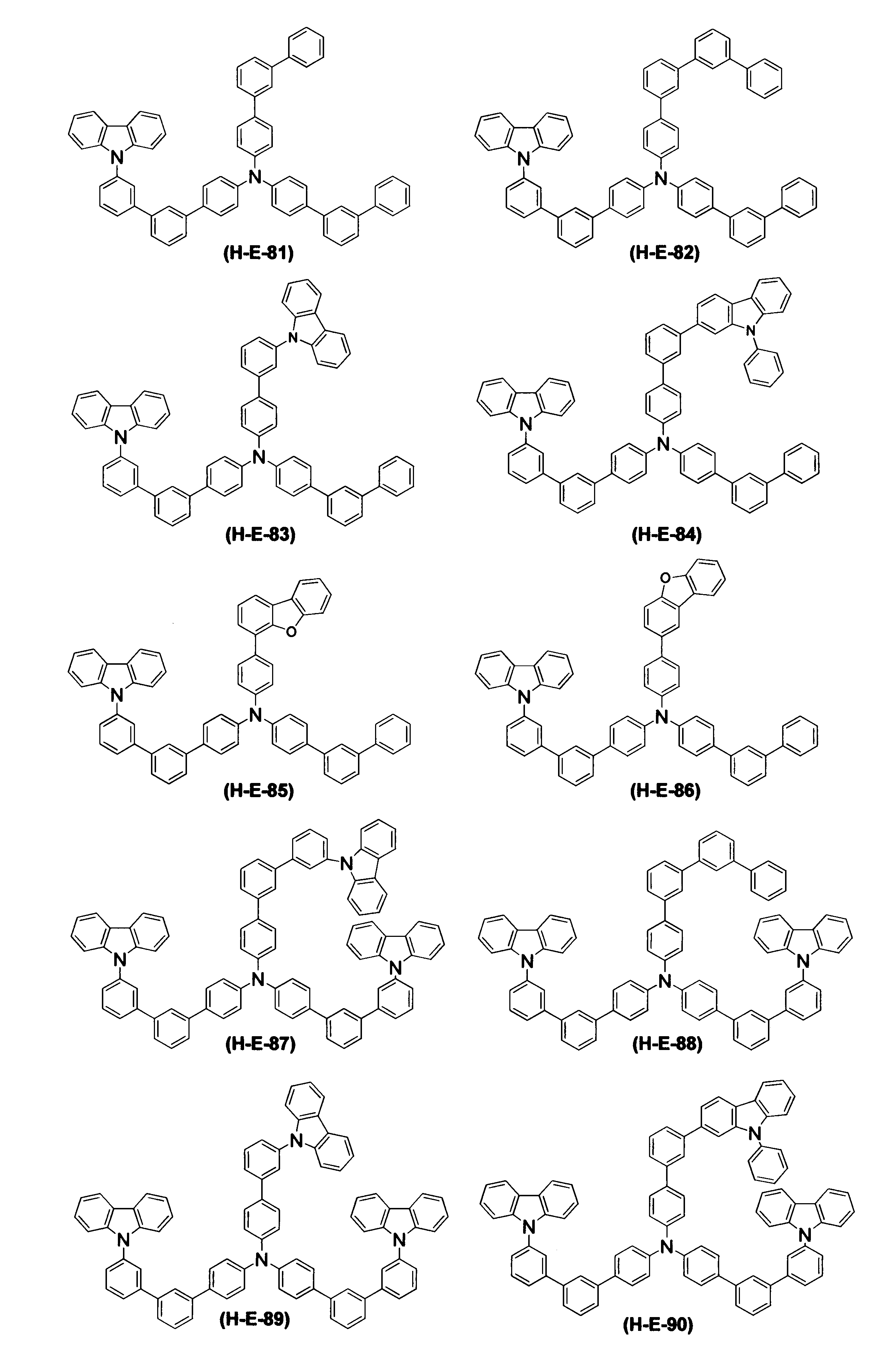
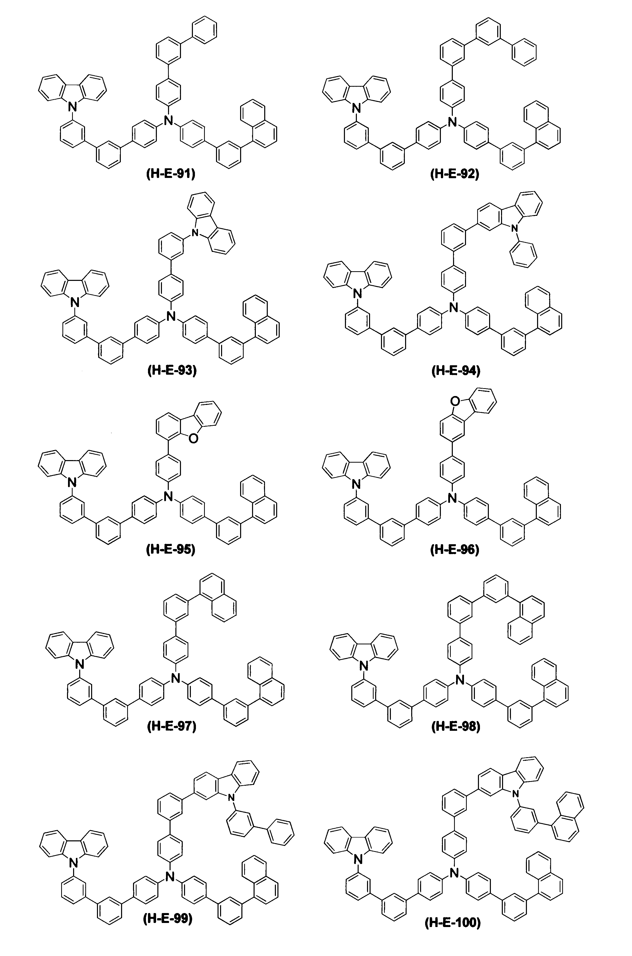


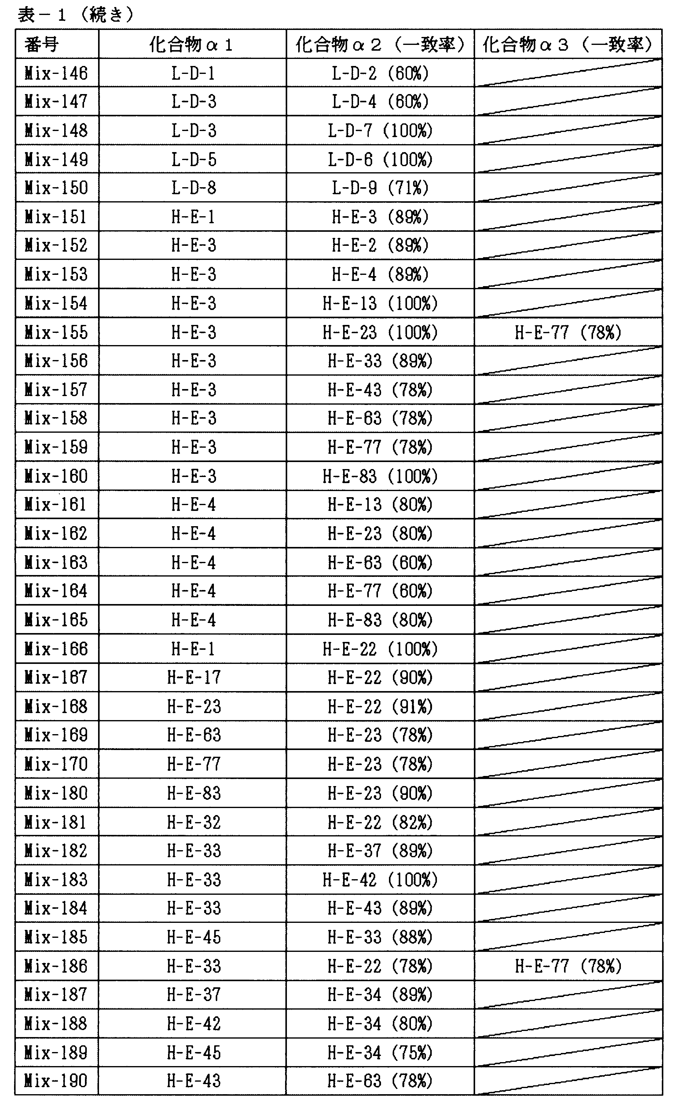
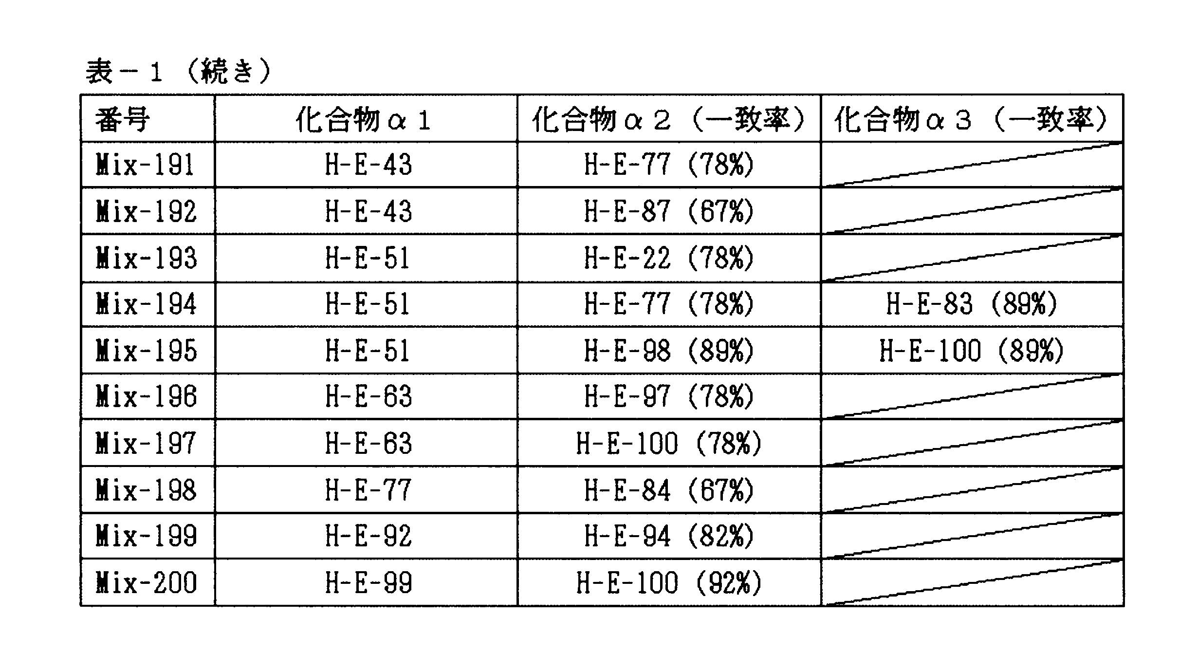

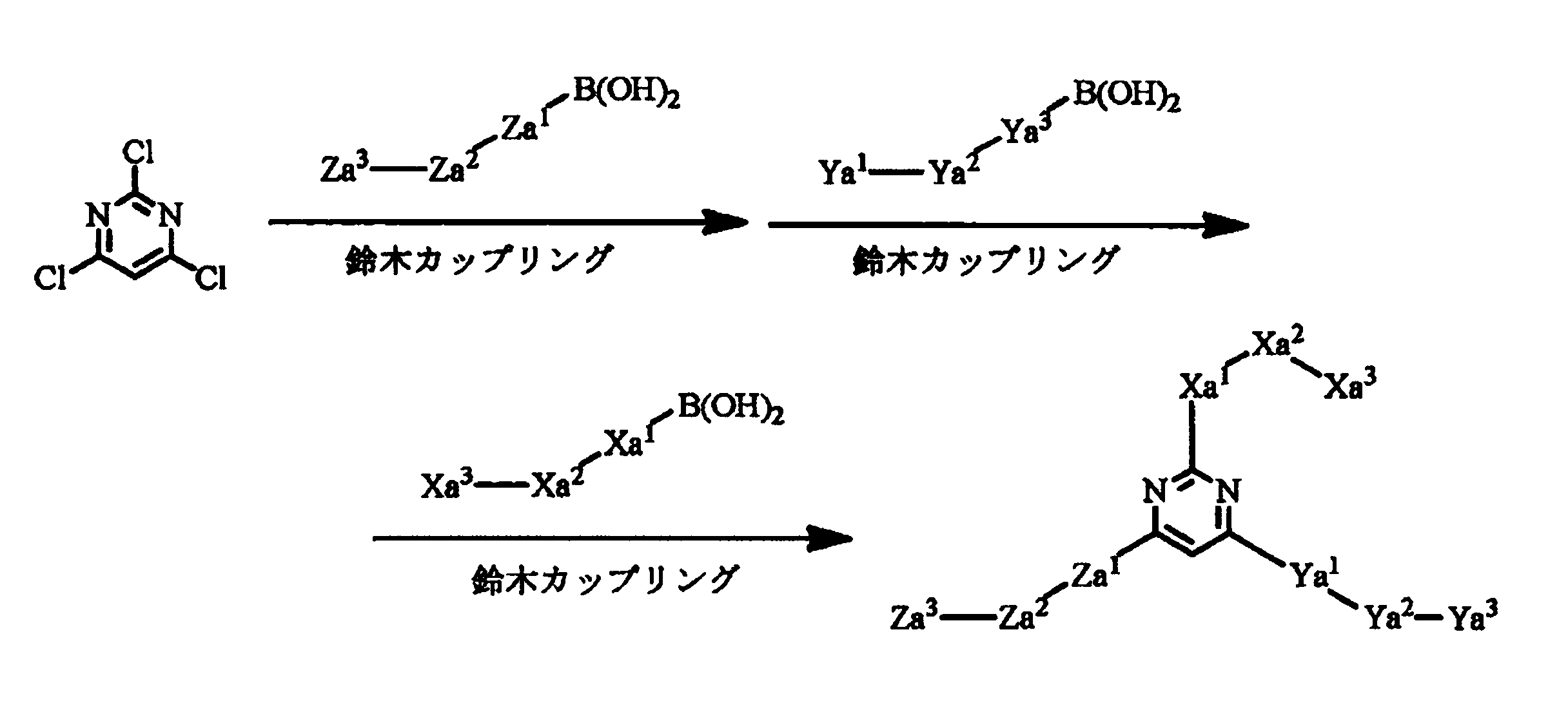


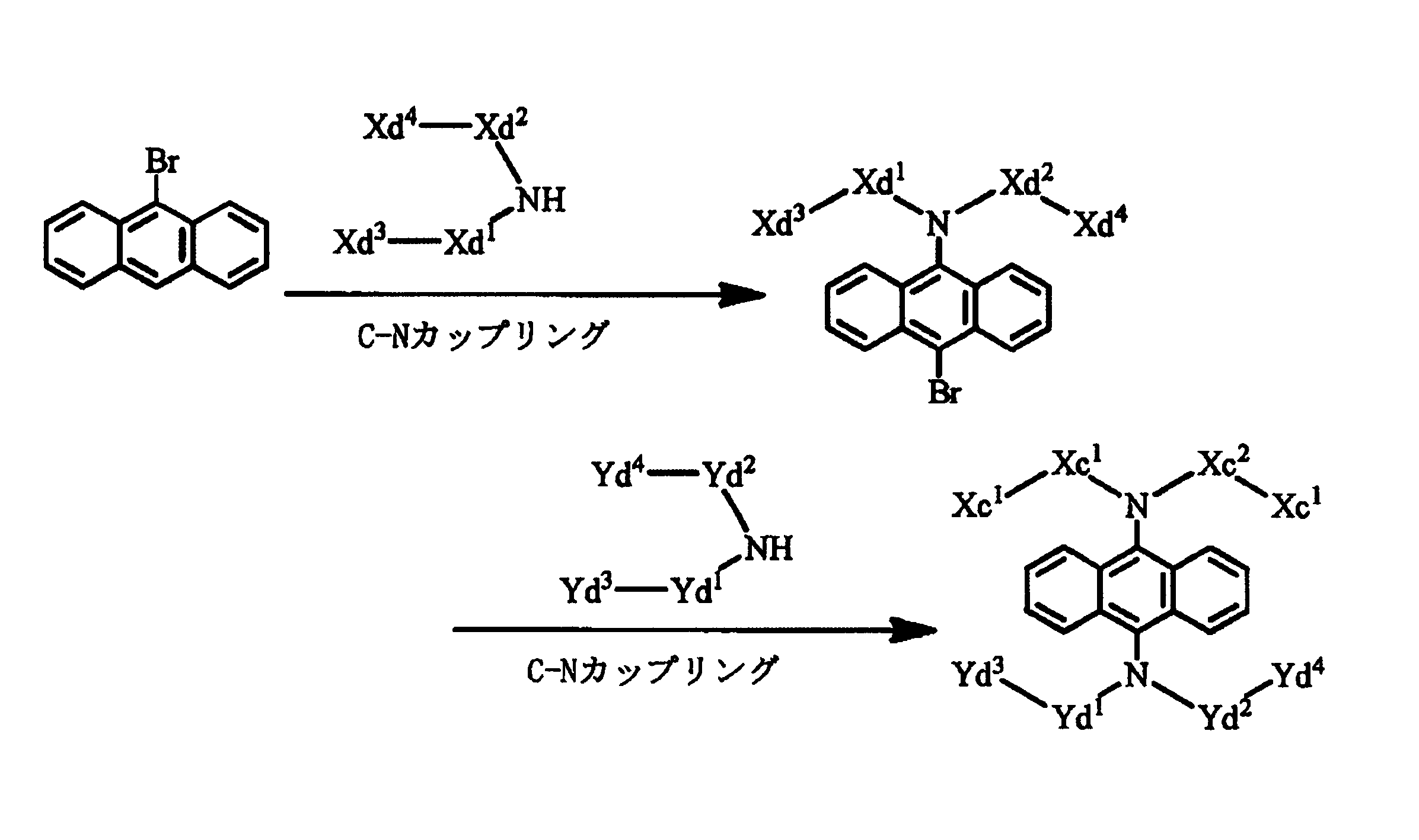

化合物群αを有機電界発光素子の発光層におけるホスト材料として使用する場合、該化合物群αの固形分中の含有量は下限は通常5重量%以上、好ましくは10重量以上であり、さらに好ましくは20重量%以上であり、上限はドーパント材料を含有するため通常99.9重量%以下である。上限値以下とすることにより高い輝度が得られ、下限値以上とすることにより素子の駆動電圧を低く抑えることができる。
一方、化合物群αを発光層におけるドーパント材料として用いる場合、該化合物群αの固形分中の含有量は、通常0.1重量%以上、好ましくは1重量%以上であり、通常50重量%以下、好ましくは30重量%以下、さらに好ましくは20重量%以下である。上限値以下とすることにより濃度消光を抑えて高い輝度を維持することができ、下限値以上とすることにより、高い発光効率を維持することができる。
本発明の有機電界発光素子用組成物は、溶剤を含有する。
溶剤としては、上述した化合物群αや、その他組成物中に含まれる各成分を溶解するものであれば特に制限は無いが、好ましい溶剤としては以下のものが挙げられる。
本発明の有機電界発光素子用組成物には、必要に応じて、上記の化合物群α及び溶剤の他に、更に他の成分を含有していてもよい。例えば、成膜性の向上を目的として、レベリング剤や消泡剤等の各種添加剤を含有していてもよい。また、化合物群αに含まれるもの以外の電荷輸送材料を含んでいてもよく、本発明の組成物を使用して、有機電界発光素子の発光層を形成する場合には、蛍光発光又は燐光発光を生じる発光材料を含有していてもよい。特に、本発明の有機電界発光素子用組成物が発光層形成用組成物であって、化合物群αが一般式(A)で表される複数の化合物からなる場合、または、化合物群αが一般式(E)で表される複数の化合物からなる場合は、燐光発光を生じる発光材料を含むことが好ましい。燐光発光を生じる材料としては、日本国特開2011-256129号公報にて開示されている遷移金属錯体が挙げられる。
本発明の有機電界発光素子は、基板上に少なくとも陽極、陰極及びこれらの両極間に設けられた発光層を有するものであって、本発明の組成物を用いて湿式成膜法により形成された層を有することを特徴とする。該湿式成膜法により形成された層は、該発光層であることが好ましい。
基板1は有機電界発光素子の支持体となるものであり、石英やガラスの板、金属板や金属箔、プラスチックフィルムやシートなどが用いられる。特にガラス板や、ポリエステル、ポリメタクリレート、ポリカーボネート、ポリスルホンなどの透明な合成樹脂の板が好ましい。合成樹脂基板を使用する場合にはガスバリア性に留意する必要がある。基板のガスバリア性が小さすぎると、基板を通過した外気により有機電界発光素子が劣化することがあるので好ましくない。このため、合成樹脂基板の少なくとも片面に緻密なシリコン酸化膜等を設けてガスバリア性を確保する方法も好ましい方法の一つである。
基板1上には陽極2が設けられる。陽極2は発光層側の層(正孔注入層3、正孔輸送層4又は発光層5など)への正孔注入の役割を果たすものである。
正孔注入層3は、陽極2から発光層5へ正孔を輸送する層であり、通常、陽極2上に形成される。本発明に係る正孔注入層3の形成方法は真空蒸着法でも、湿式成膜法でもよく、特に制限はないが、ダークスポット低減の観点から正孔注入層3を湿式成膜法により形成することが好ましい。正孔注入層3の膜厚は、通常5nm以上、好ましくは10nm以上、また、通常1000nm以下、好ましくは500nm以下の範囲である。
湿式成膜により正孔注入層3を形成する場合、通常は、正孔注入層3を構成する材料を適切な溶剤(正孔注入層用溶剤)と混合して成膜用の組成物(正孔注入層形成用組成物)を調製し、この正孔注入層形成用組成物を適切な手法により、正孔注入層3の下層に該当する層(通常は、陽極)上に塗布して成膜し、乾燥することにより正孔注入層3を形成する。
正孔注入層形成用組成物は通常、正孔注入層の構成材料として正孔輸送性化合物及び溶剤を含有する。正孔輸送性化合物は、通常、有機電界発光素子の正孔注入層に使用される、正孔輸送性を有する化合物であれば、重合体などの高分子化合物であっても、単量体などの低分子化合物であってもよいが、高分子化合物であることが好ましい。
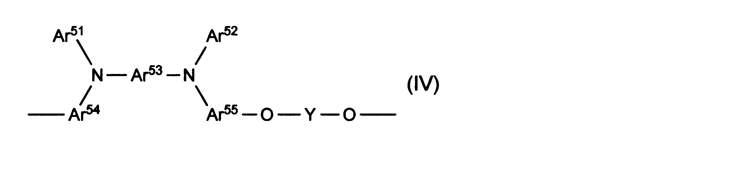
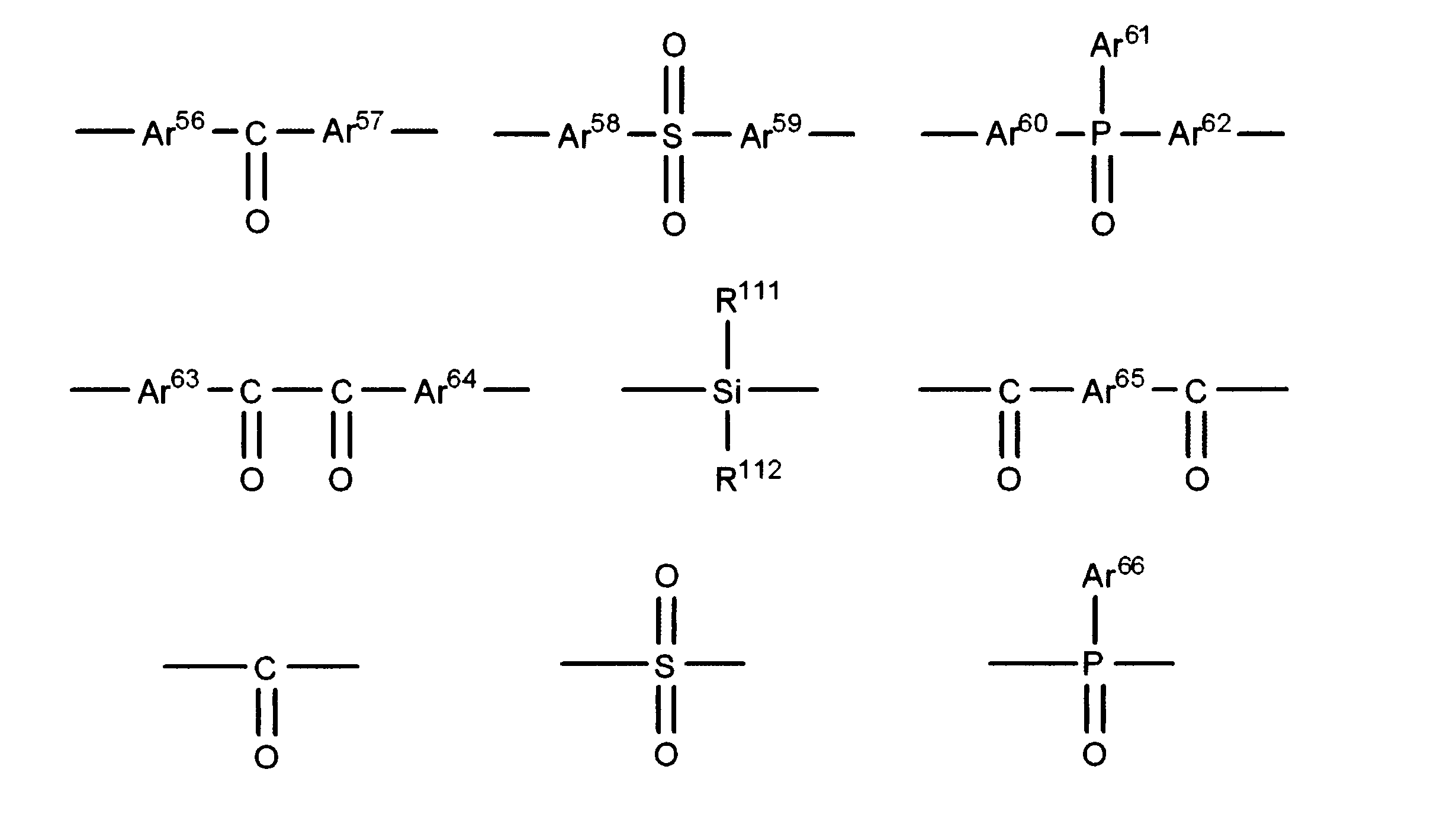
正孔注入層形成用組成物は正孔注入層の構成材料として、電子受容性化合物を含有していることが好ましい。
湿式成膜法に用いる正孔注入層形成用組成物の溶剤のうち少なくとも1種は、上述の正孔注入層の構成材料を溶解しうる化合物であることが好ましい。また、この溶剤の沸点は通常110℃以上、好ましくは140℃以上、中でも200℃以上、通常400℃以下、中でも300℃以下であることが好ましい。溶剤の沸点が低すぎると、乾燥速度が速すぎ、膜質が悪化する可能性がある。また、溶剤の沸点が高すぎると乾燥工程の温度を高くする必要があり、他の層や基板に悪影響を与える可能性がある。
正孔注入層形成用組成物を調製後、この組成物を湿式成膜により、正孔注入層3の下層に該当する層(通常は、陽極2)上に塗布成膜し、乾燥することにより正孔注入層3を形成する。
塗布工程における相対湿度は、本発明の効果を著しく損なわない限り限定されないが、通常0.01ppm以上、通常80%以下である。
真空蒸着により正孔注入層3を形成する場合には、正孔注入層3の構成材料(前述の正孔輸送性化合物、電子受容性化合物等)の1種又は2種以上を真空容器内に設置されたるつぼに入れ(2種以上の材料を用いる場合は各々のるつぼに入れ)、真空容器内を適当な真空ポンプで10-4Pa程度まで排気した後、るつぼを加熱して(2種以上の材料を用いる場合は各々のるつぼを加熱して)、蒸発量を制御して蒸発させ(2種以上の材料を用いる場合は各々独立に蒸発量を制御して蒸発させ)、るつぼと向き合って置かれた基板の陽極2上に正孔注入層3を形成させる。なお、2種以上の材料を用いる場合は、それらの混合物をるつぼに入れ、加熱、蒸発させて正孔注入層3を形成することもできる。
正孔輸送層4は、正孔注入層がある場合には正孔注入層3の上に、正孔注入層3が無い場合には陽極2の上に形成することができる。また、本発明の有機電界発光素子は、正孔輸送層を省いた構成であってもよい。
中でも、ポリアリールアミン誘導体やポリアリーレン誘導体が好ましい。

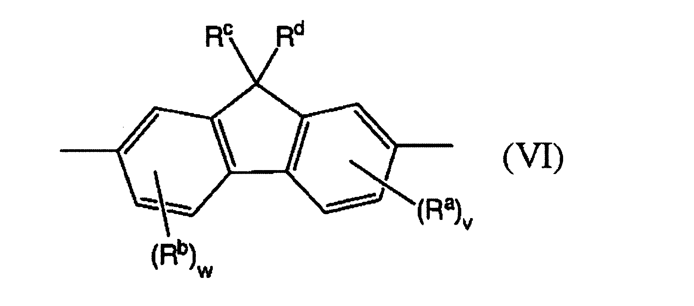
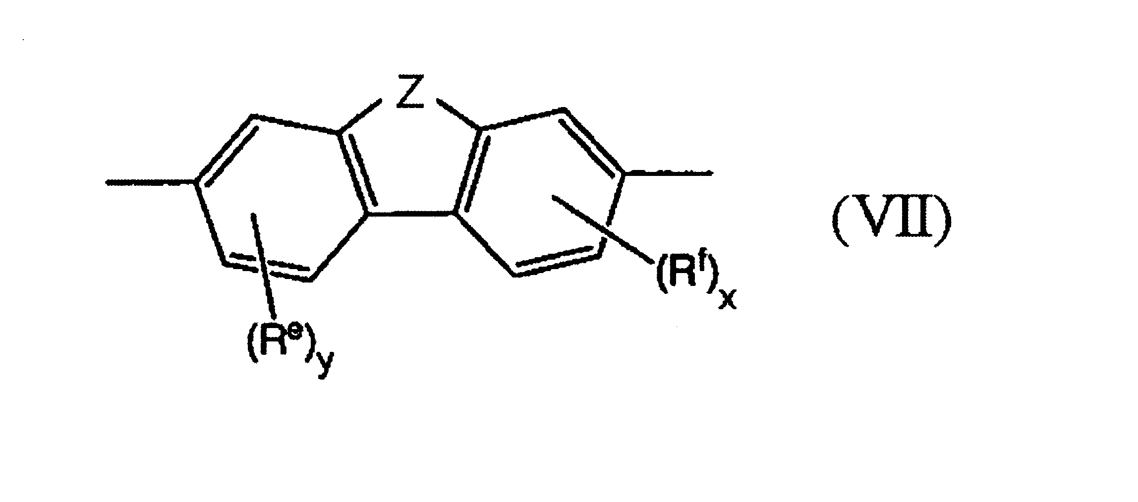
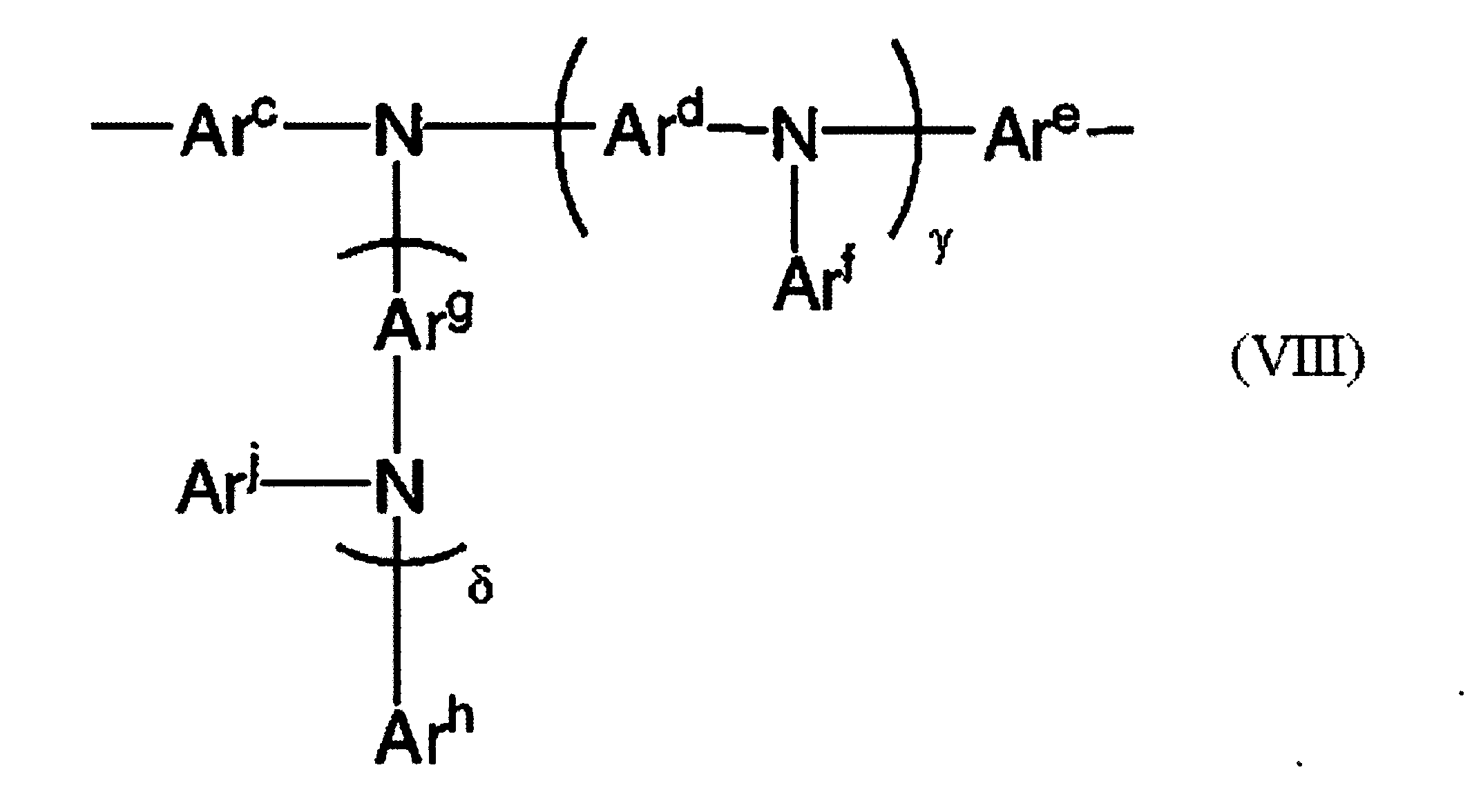
正孔輸送層4の上には通常、発光層5が設けられる。発光層5は、電界を与えられた電極間において、陽極2から正孔注入層3を通じて注入された正孔と、陰極9から電子輸送層7を通じて注入された電子との再結合により励起された、主たる発光源となる層である。発光層5は発光材料(ドーパント)と1種又は2種以上のホスト材料を含むことが好ましく、発光層5は本発明の化合物群αを含むことがさらに好ましい。発光層5は、真空蒸着法で形成してもよいが、本発明の有機電界発光素子用組成物を用い、湿式成膜法によって作製された層であることが特に好ましい。
正孔阻止層6は、発光層5の上に、発光層5の陰極側の界面に接するように積層形成される。特に、発光物質として燐光材料を用いたり、青色発光材料を用いたりする場合、正孔阻止層6を設けることは効果的である。正孔阻止層6は正孔と電子を発光層5内に閉じこめて、発光効率を向上させる機能を有する。即ち、正孔阻止層6は、発光層5から移動してくる正孔が電子輸送層7に到達するのを阻止することで、発光層5内で電子との再結合確率を増やし、生成した励起子を発光層5内に閉じこめる役割と、電子輸送層7から注入された電子を効率よく発光層5の方向に輸送する役割がある。
電子輸送層7は素子の発光効率をさらに向上させることを目的として、正孔注入層6と電子注入層8との間に設けられる。電子輸送層7は、電界を与えられた電極間において陰極9から注入された電子を効率よく発光層5の方向に輸送することができる化合物より形成される。電子輸送層7に用いられる電子輸送性化合物としては、陰極9又は電子注入層8からの電子注入効率が高く、かつ、高い電子移動度を有し注入された電子を効率よく輸送することができる化合物であることが必要である。
電子注入層8は陰極9から注入された電子を効率よく発光層5へ注入する役割を果たす。電子注入を効率よく行うには、電子注入層8を形成する材料は、仕事関数の低い金属が好ましく、ナトリウムやセシウム等のアルカリ金属、バリウムやカルシウムなどのアルカリ土類金属が用いられる。電子注入層8の膜厚は0.1~5nmが好ましい。
陰極9は、発光層側の層(電子注入層8又は発光層5など)に電子を注入する役割を果たす。陰極9として用いられる材料は、前記陽極2に使用される材料を用いることも可能であるが、効率よく電子注入を行うには、仕事関数の低い金属が好ましく、スズ、マグネシウム、インジウム、カルシウム、アルミニウム、銀等の適当な金属又はそれらの合金が用いられる。具体例としては、マグネシウム-銀合金、マグネシウム-インジウム合金、アルミニウム-リチウム合金等の低仕事関数合金電極が挙げられる。
以上、図1に示す層構成の素子を中心に説明してきたが、本発明の有機電界発光素子における陽極2及び陰極9と発光層5との間には、その性能を損なわない限り、上記説明にある層の他にも、任意の層を有していてもよく、また発光層5以外の任意の層を省略してもよい。
本発明の表示装置及び照明装置は、上述のような本発明の有機電界発光素子を用いたものである。本発明の表示装置及び照明装置の形式や構造については特に制限はなく、本発明の有機電界発光素子を用いて常法に従って組み立てることができる。
例えば、「有機ELディスプレイ」(オーム社、平成16年8月20日発光、時任静士、安達千波矢、村田英幸著)に記載されているような方法で、本発明の表示装置および照明装置を形成することができる。
(中間体1の合成)
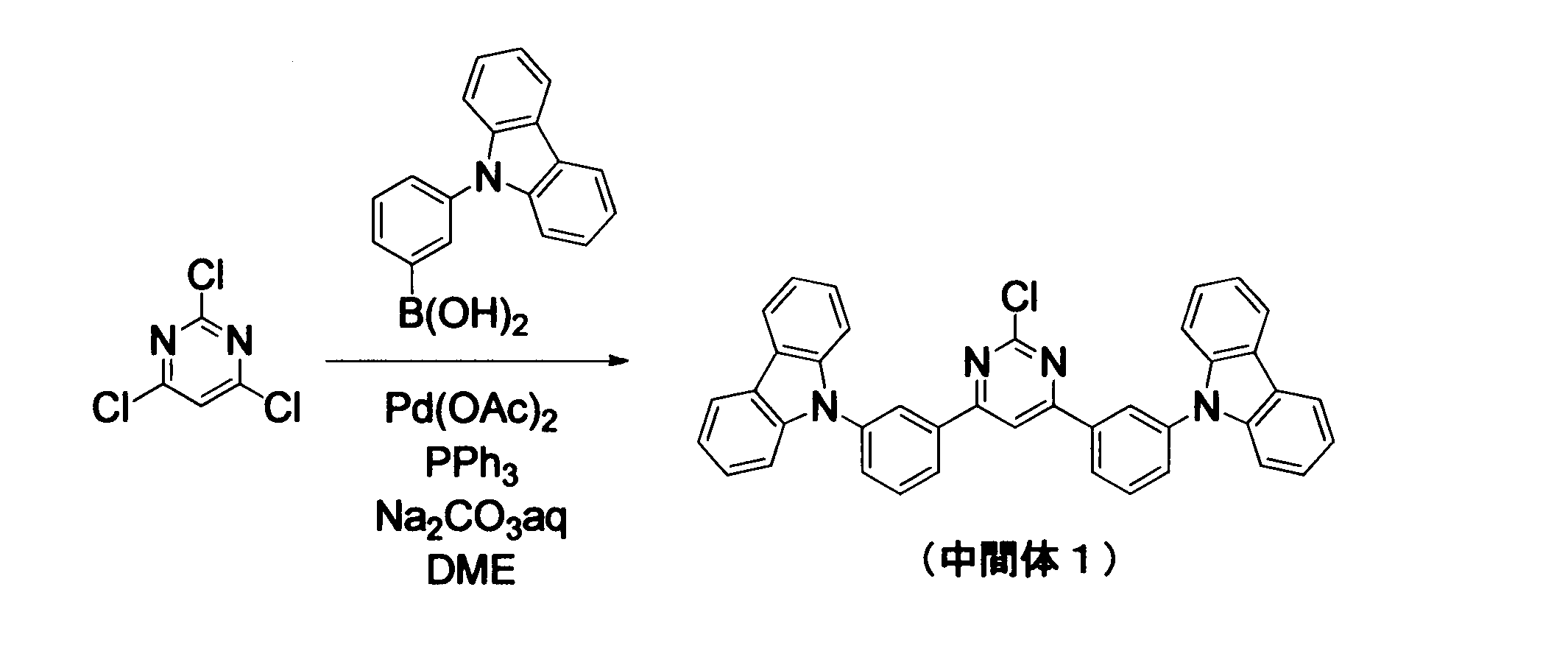

(中間体2の合成)

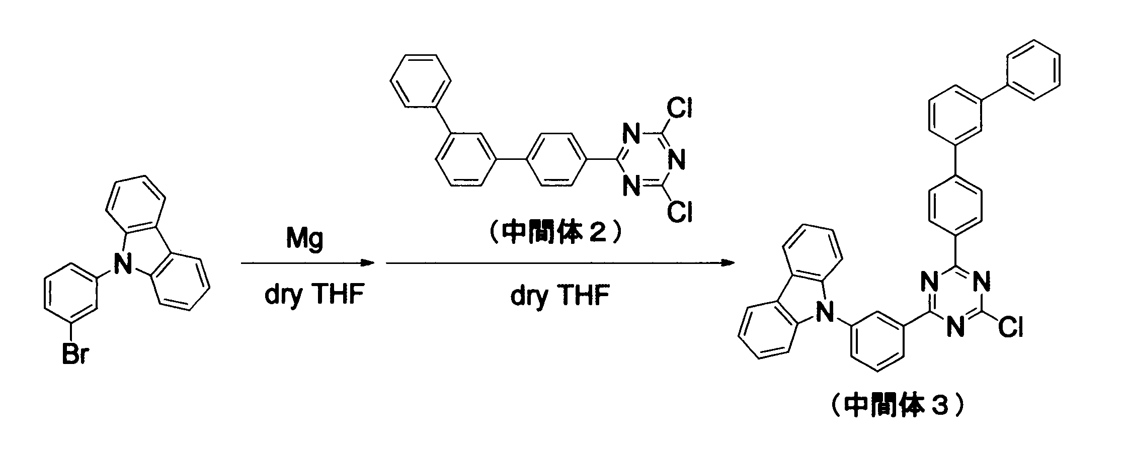
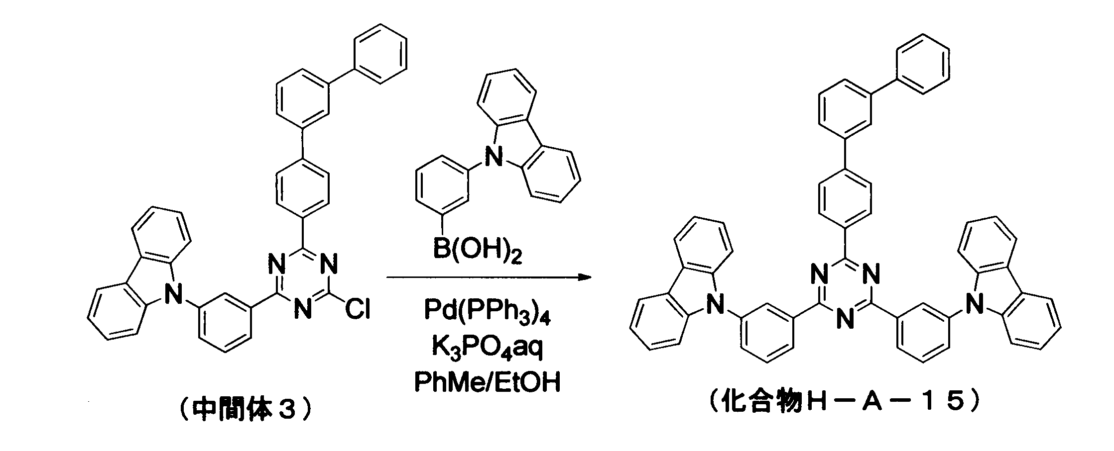
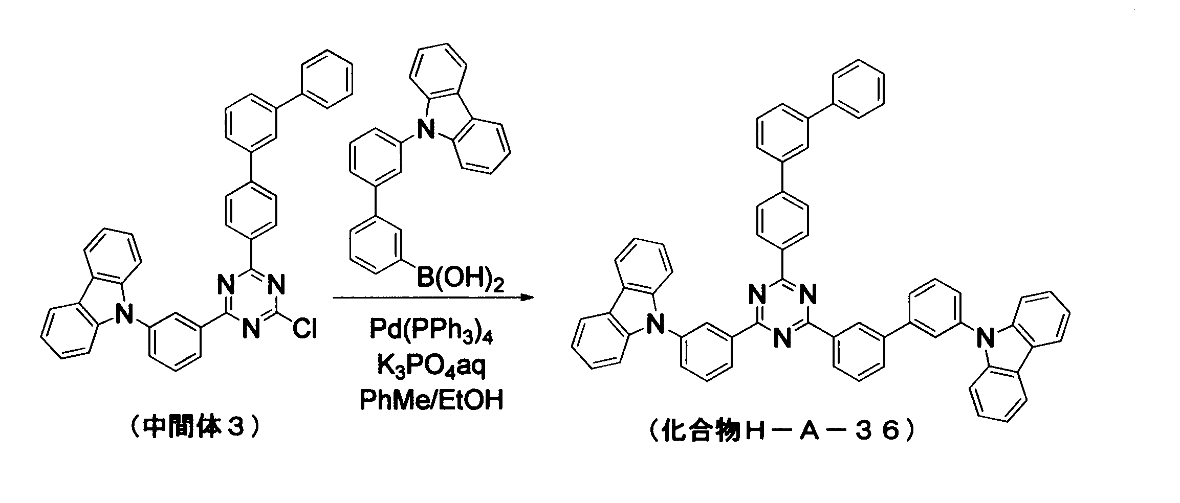
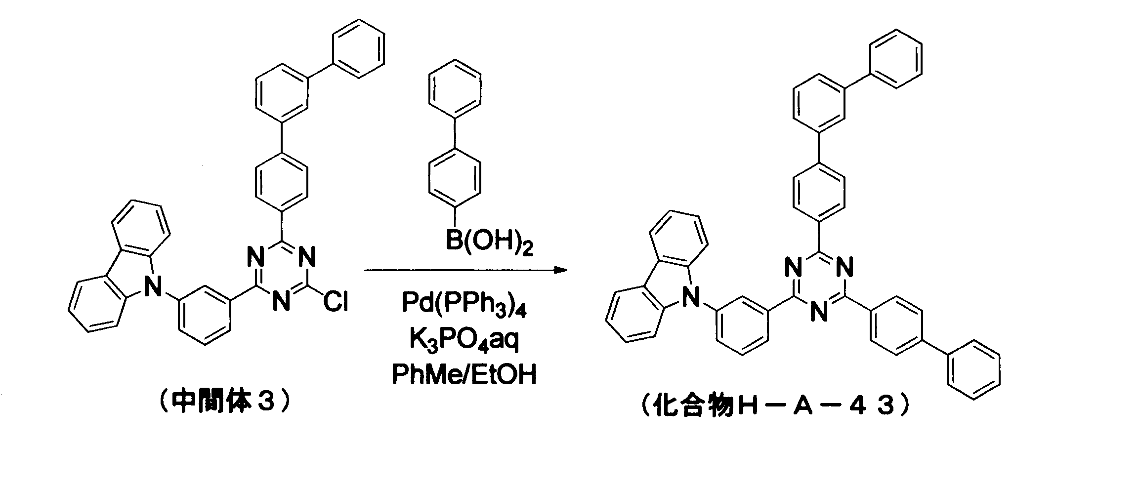
(中間体4の合成)
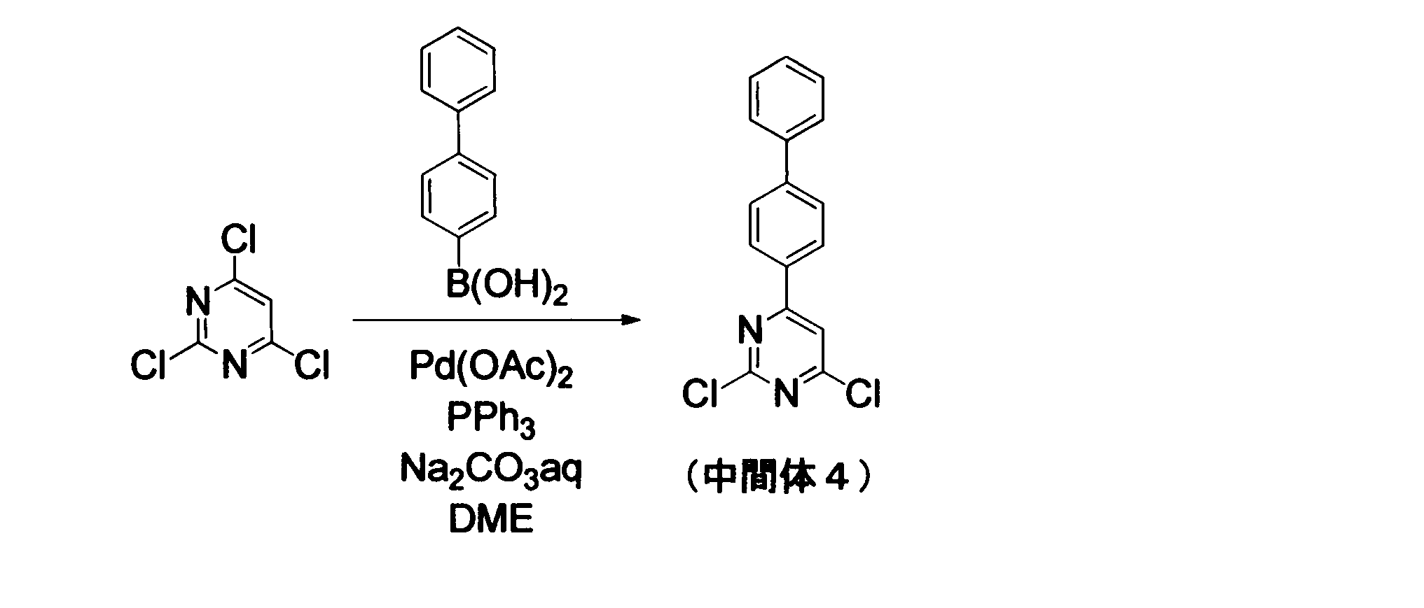

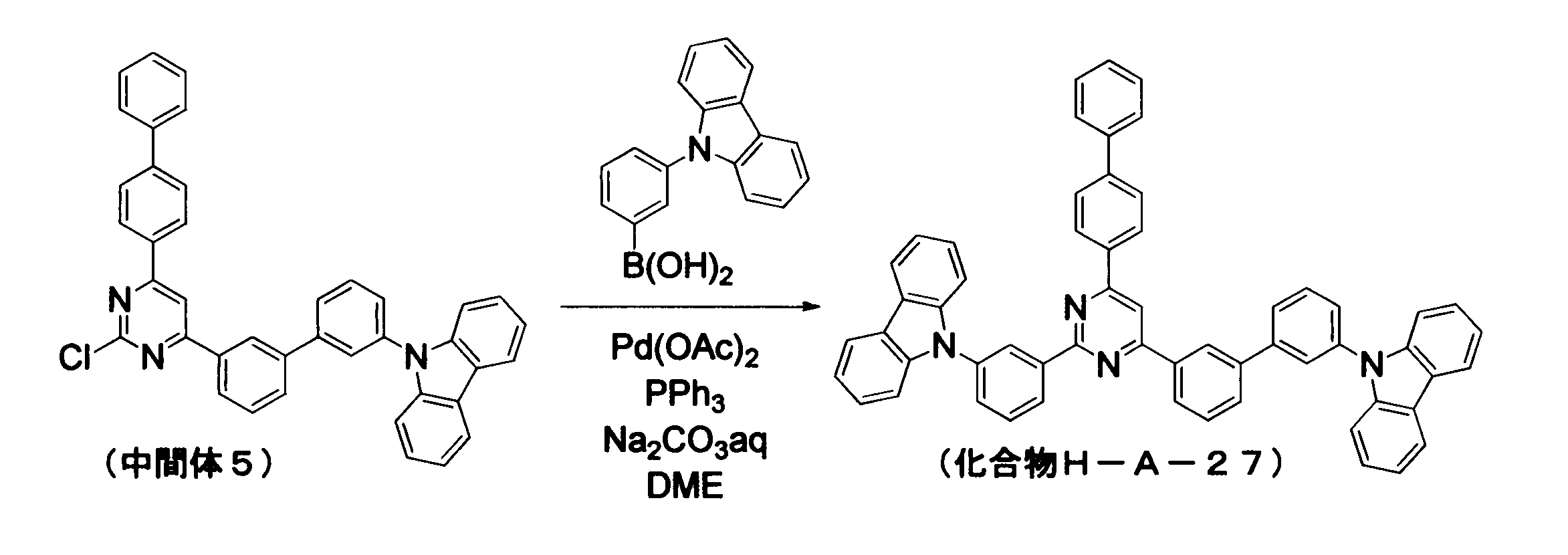
(中間体6の合成)

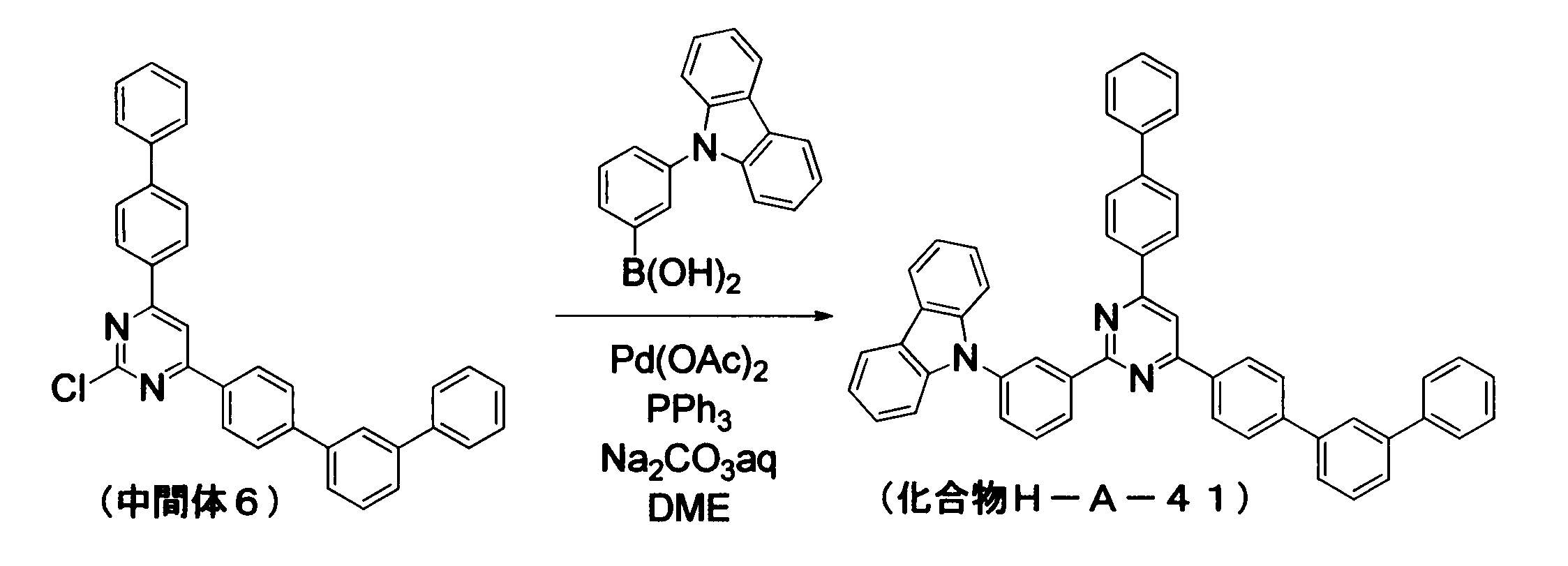
(中間体7の合成)
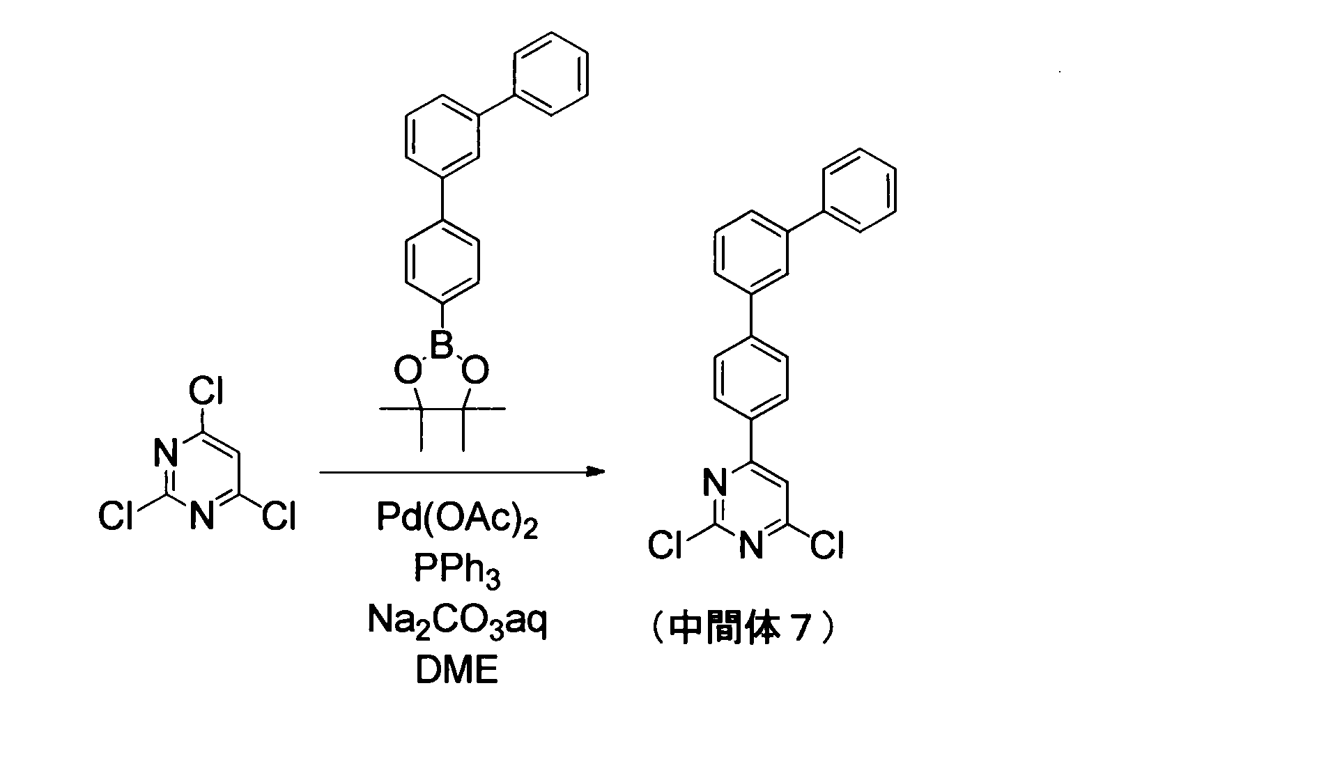
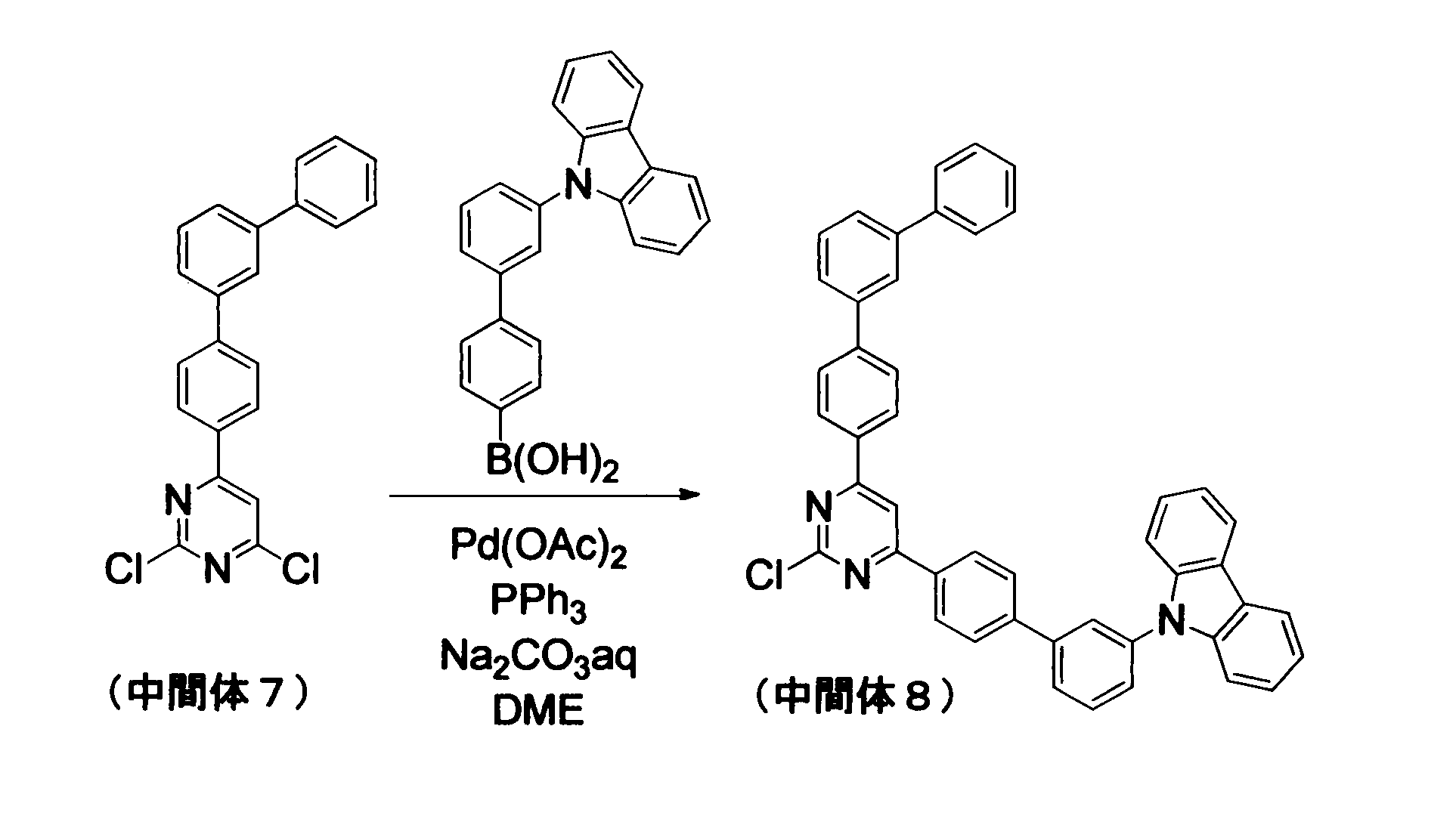
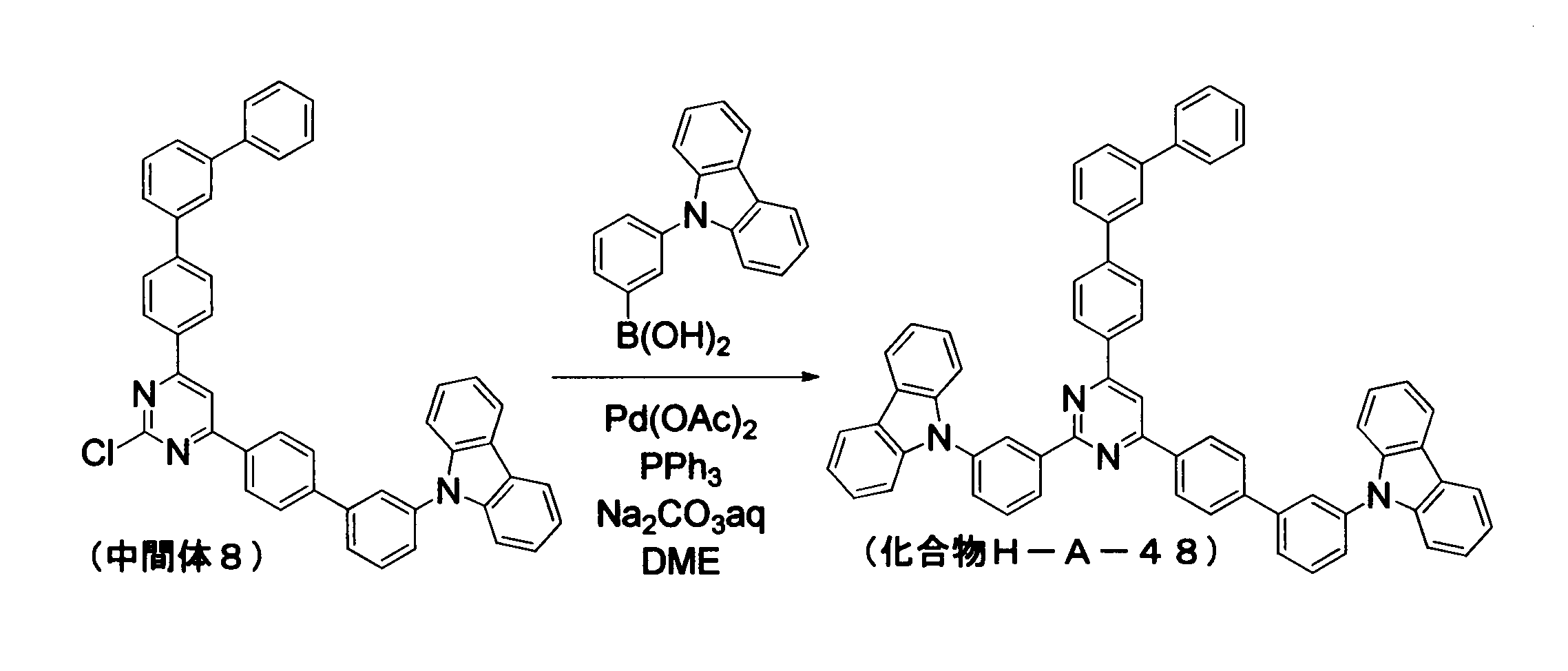
(中間体9の合成)
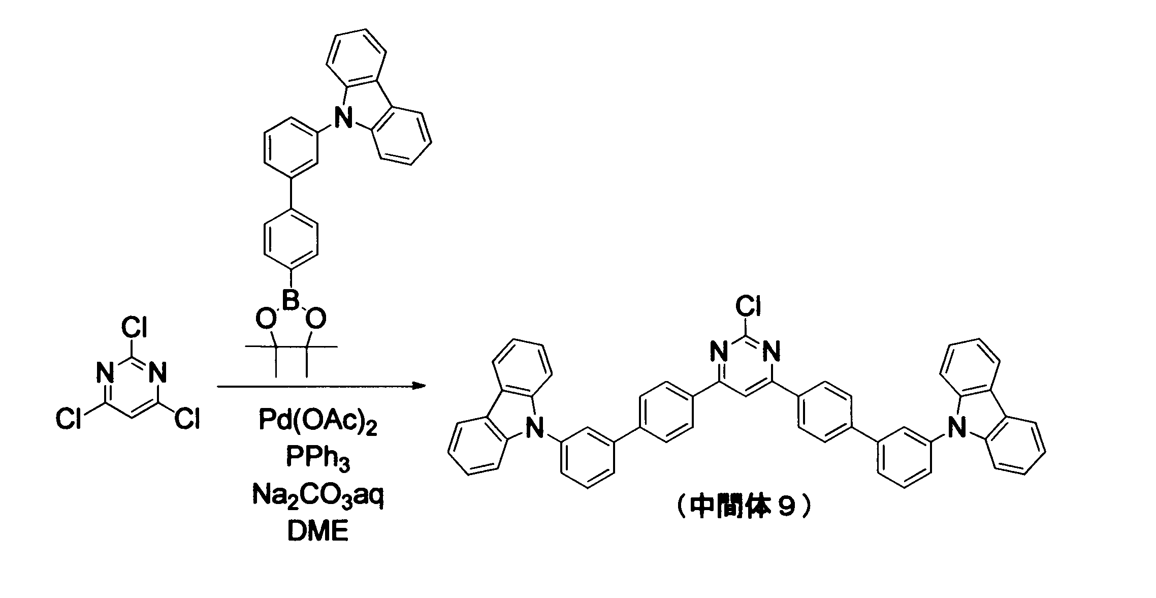
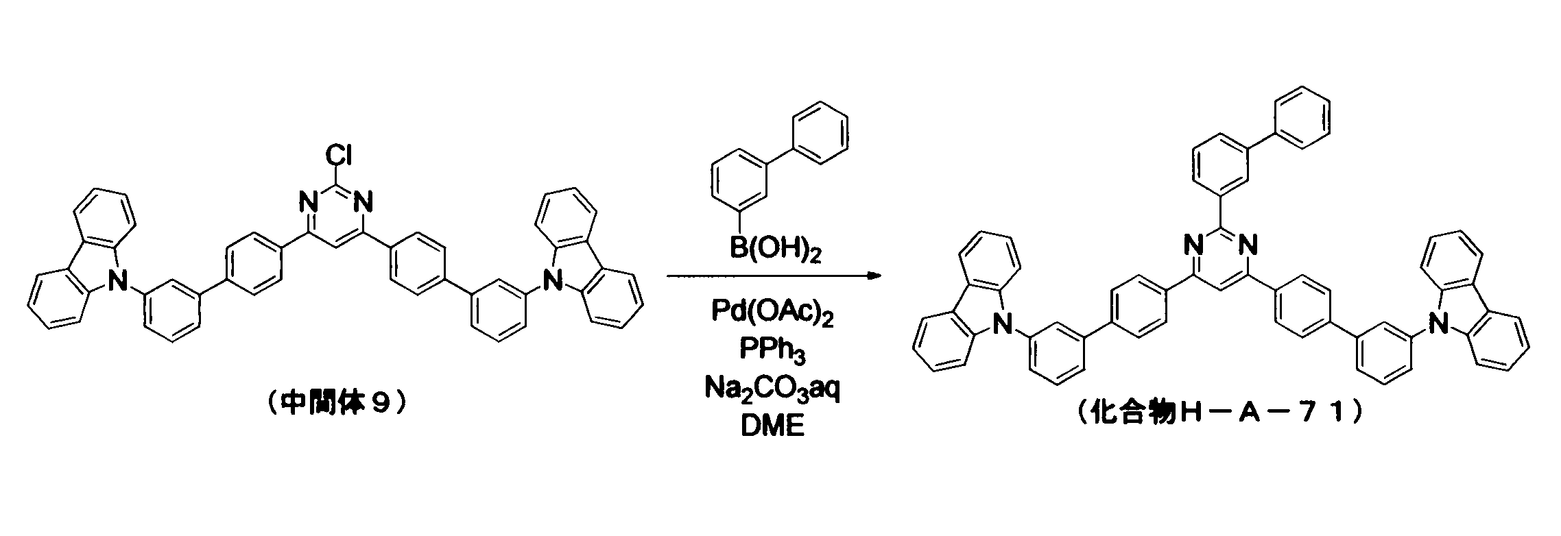
(中間体10の合成)
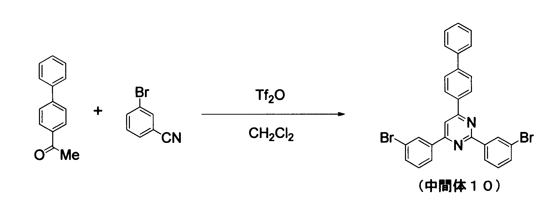
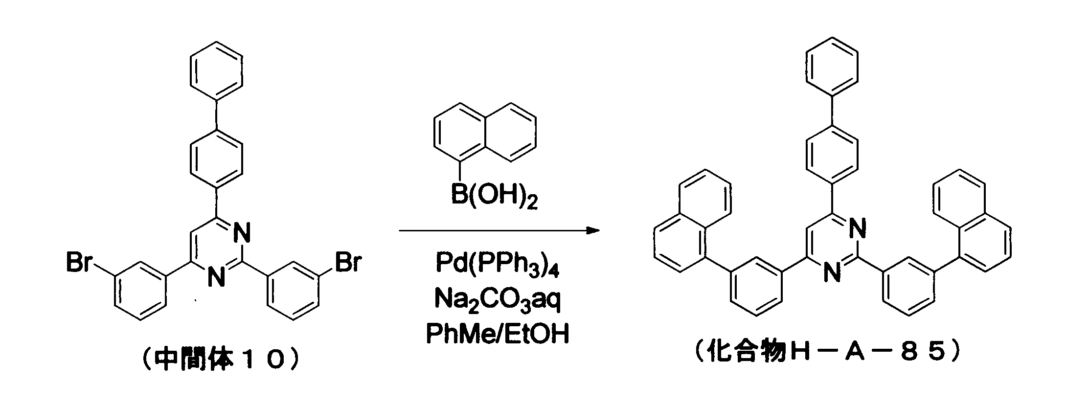
(化合物H-B-14の合成)

(中間体14の合成)

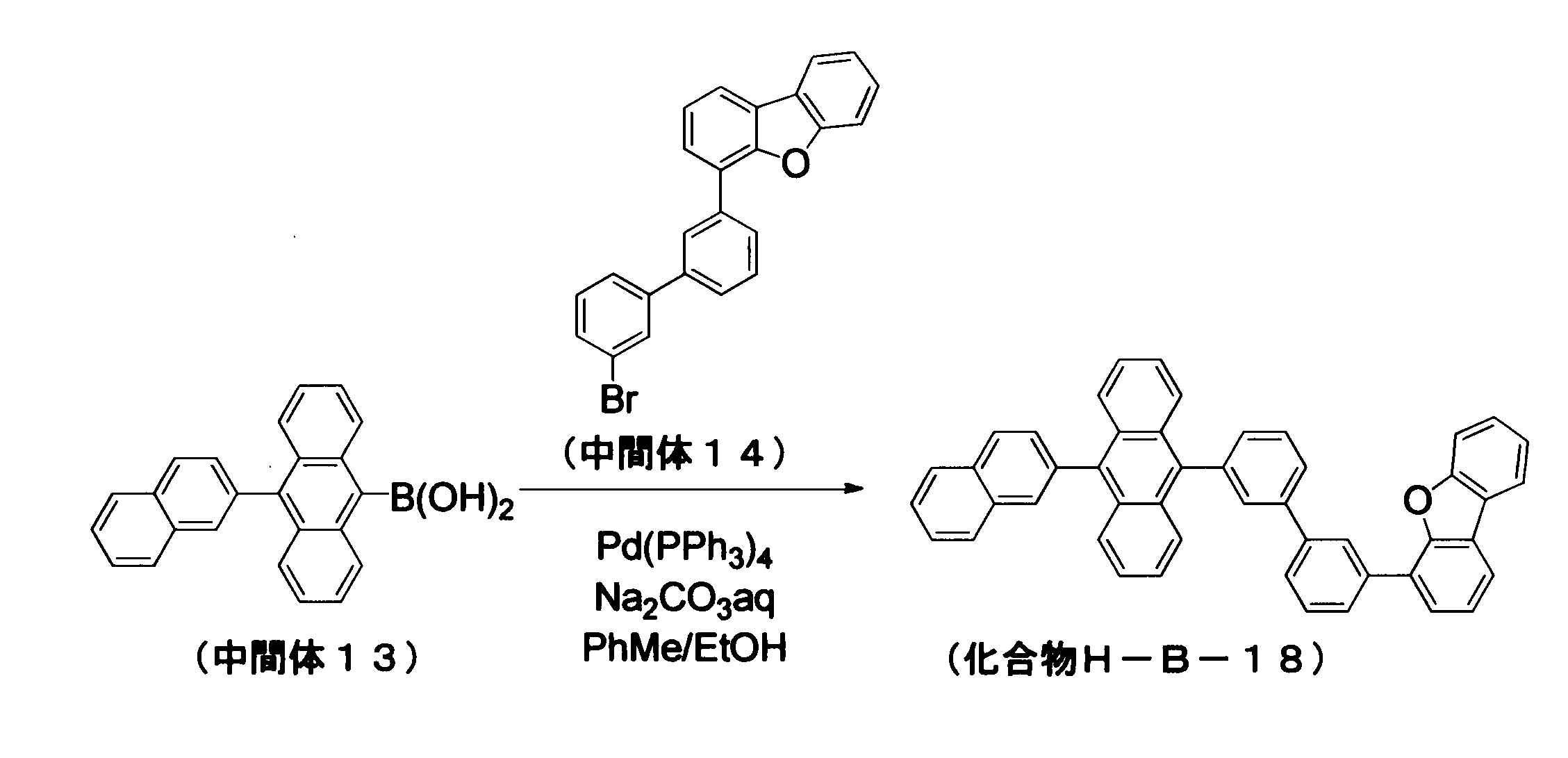
(中間体16の合成)
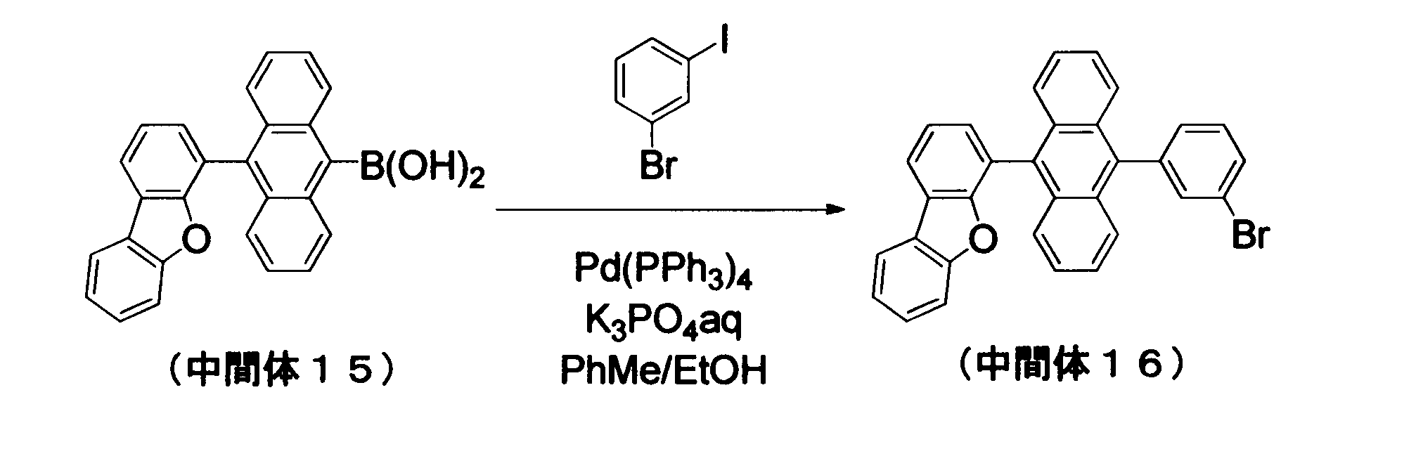
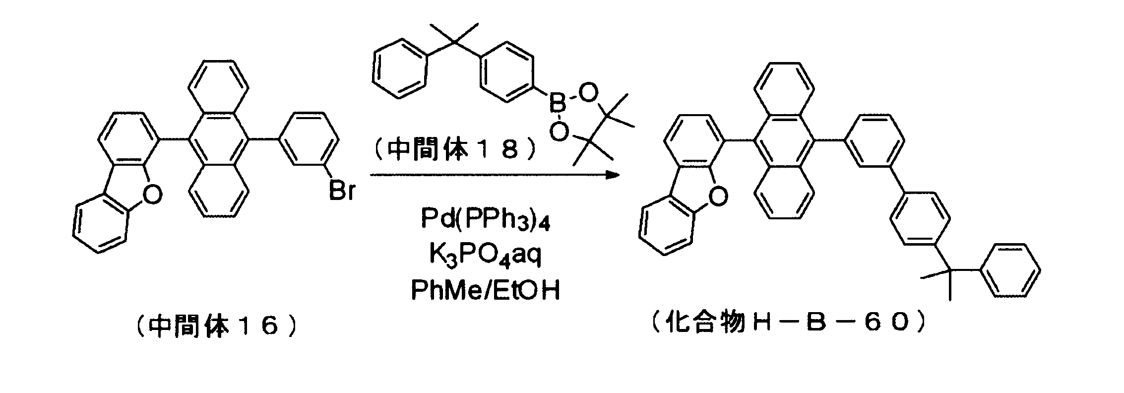
(中間体19の合成)

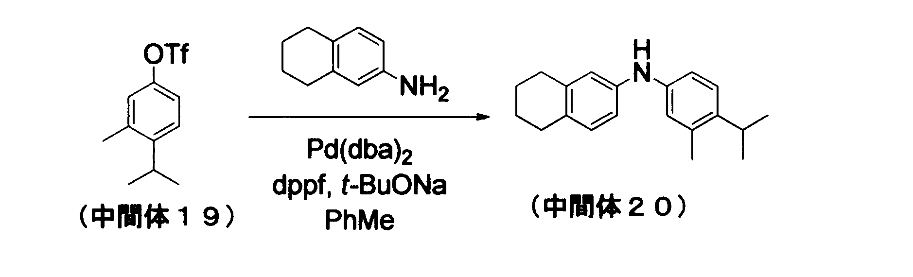
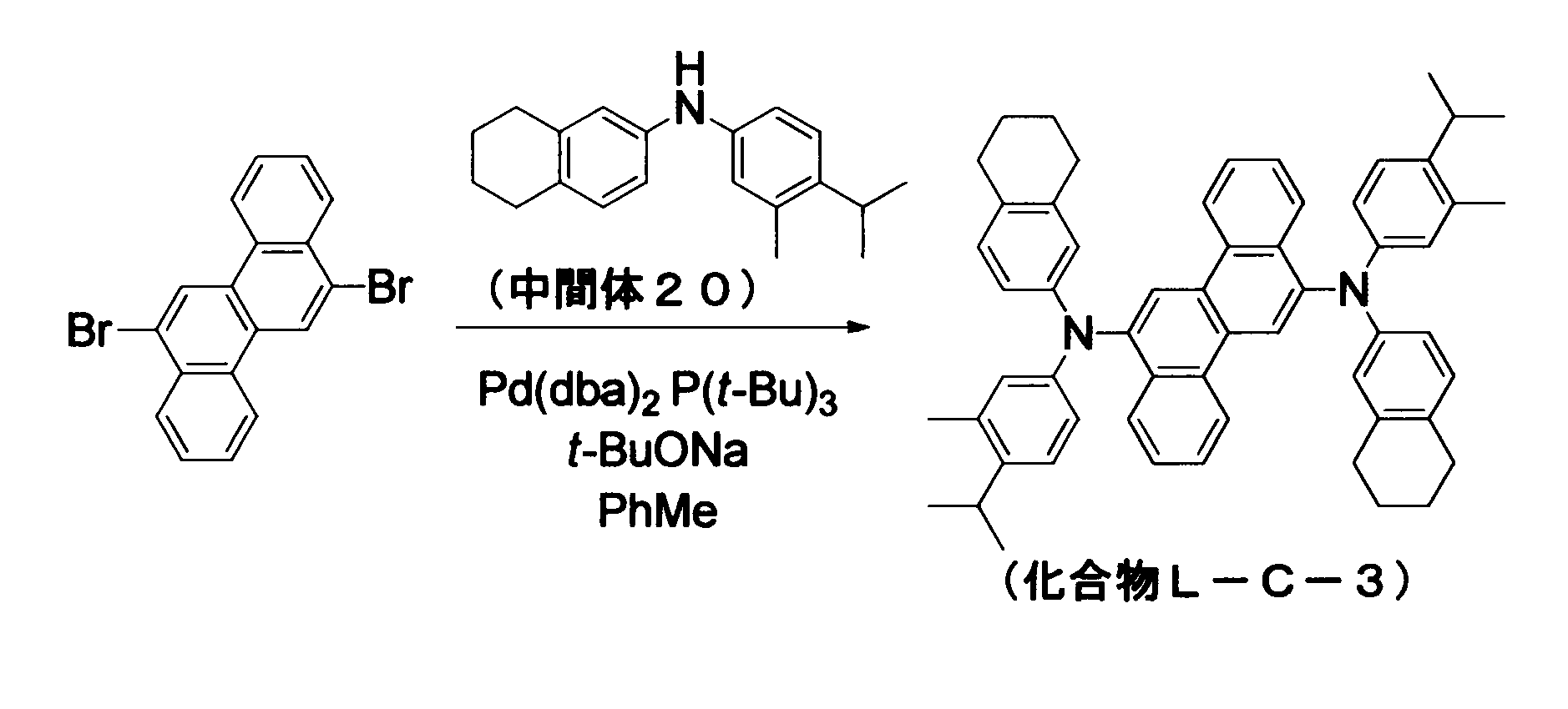
(中間体21の合成)
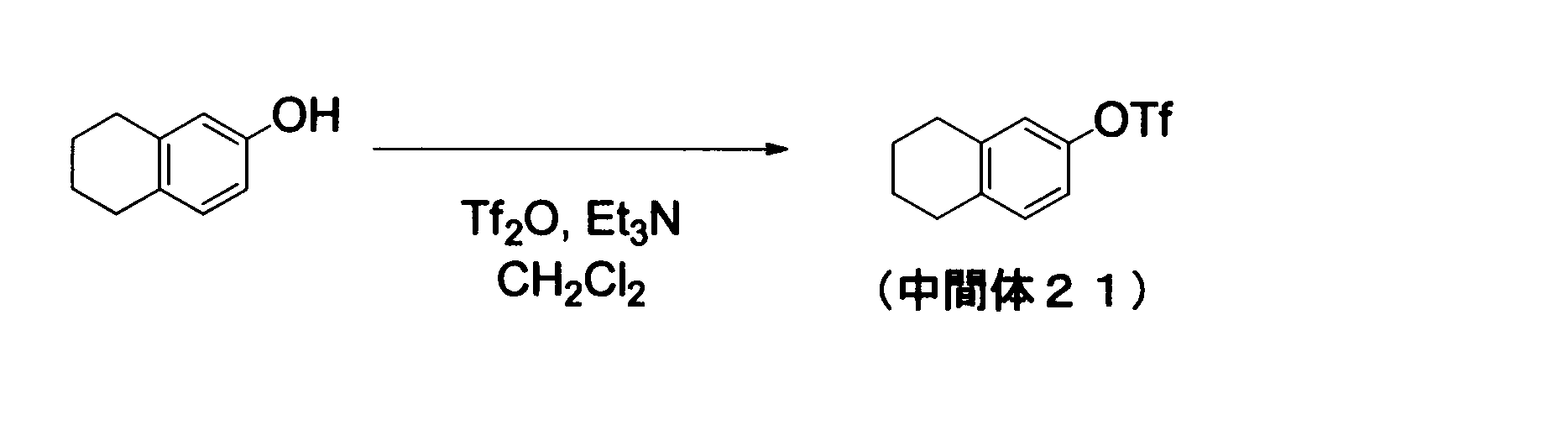
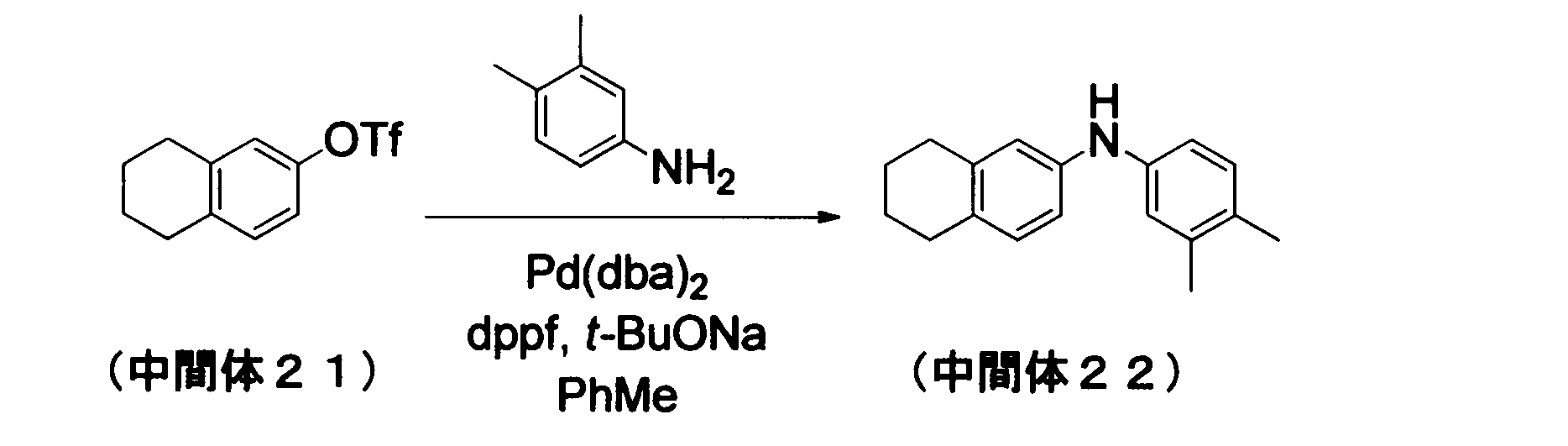
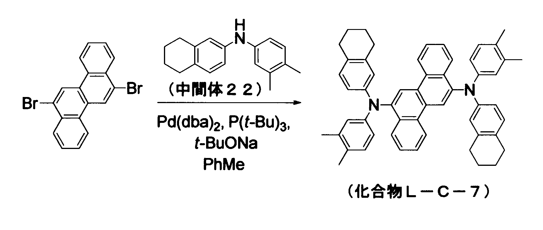
(中間体23の合成)

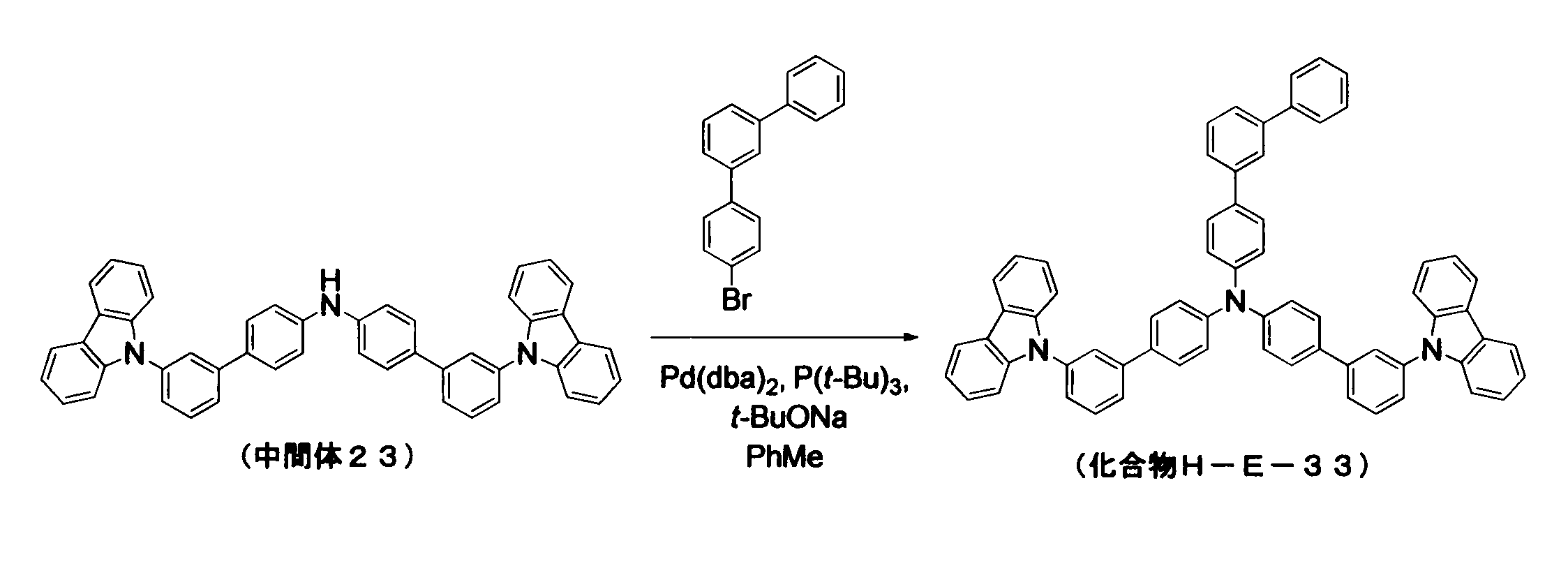

前記例示化合物に含まれる以下の材料について、下記に示す方法により有機溶剤に溶解し、組成物を調製した。
褐色サンプル瓶に、化合物(H-A-3)を2.5mg、化合物(H-A-41)を2.5mg量りとり、シクロへキシルベンゼンを加えて415mgとした後、ホットプレートを用いて120℃に加熱し、化合物(H-A-3)及び化合物(H-A-41)を完全に溶解させ、化合物(H-A-3)と化合物(H-A-41)の1:1混合物(化合物群α)を含有する組成物(固形分濃度:1.2重量%)を調製した。このとき、芳香環基の数の少ない化合物(H-A-3)が化合物α1に相当する。調製した組成物は、室温約15~20℃の暗所に置き、固体が析出するまでの時間を測定した。固体は10倍のルーペを用いて目視にて確認を行い、その結果を表2にまとめた。
実施例1において化合物(H-A-3)及び化合物(H-A-41)を表2に示した化合物および組成に置き換えたほかは、実施例1と同様の固形分濃度にて組成物を調製し、固体が析出するまでの時間を測定した。固体は10倍のルーペを用いて目視にて確認を行い、結果を表2にまとめた。なお、H-A-6ならびにH-A-11は、日本国特開2006-188493号公報にて開示された方法を参考にして得た。

褐色サンプル瓶に、化合物群α(化合物(H-A-3)及び化合物(H-A-41)の1:1混合物)、化合物(H-E-23)、下記化合物(L-1)を含有する組成物を調製した。該組成物は、有機電界発光素子において緑色発光層用塗布液として用いることができる。該組成物を一週間保存した組成物を用いて有機電界発光素子を作製した。なお、H-E-23、L-1は、それぞれ、日本国特開2010-206191号公報、日本国特開2010-202644号公報にて開示されている方法にて調製した。
溶媒 シクロヘキシルベンゼン
固形分濃度 化合物群α 1.2重量%
H-E-23 3.6重量%
L-1 0.48重量%
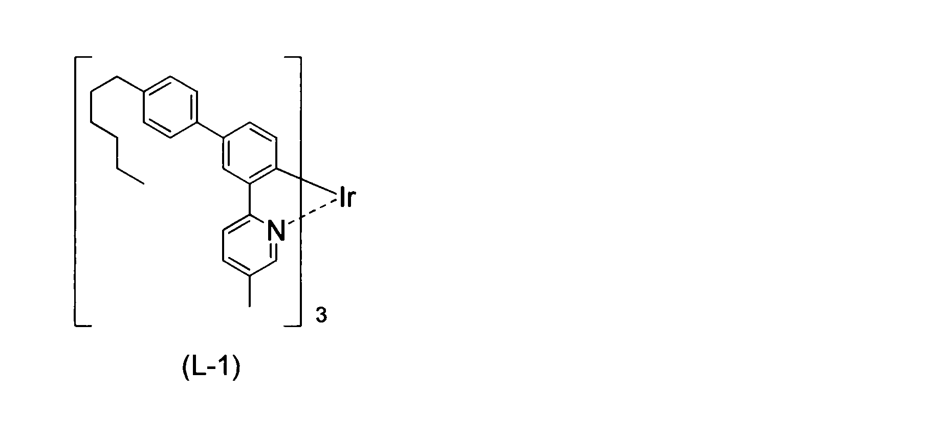
<有機電界発光素子の作製>
ガラス基板上1の上に、インジウム・スズ酸化物(ITO)透明導電膜を70nmの厚さに堆積したもの(ジオマテック社製、スパッタ成膜品)を、通常のフォトリソグラフィー技術と塩酸エッチングを用いて2mm幅のストライプにパターニングして陽極2を形成した。パターン形成したITO基板を、界面活性剤水溶液による超音波洗浄、超純水による水洗、超純水による超音波洗浄、超純水による水洗の順で洗浄後、圧縮空気で乾燥させ、最後に紫外線オゾン洗浄を行った。このITOは、透明電極2として機能する。

溶媒 安息香酸エチル
塗布液濃度 P-1 2.5重量%
A-10 0.5重量%
<正孔注入層3の成膜条件>
スピンコート雰囲気 大気中
加熱条件 大気中 230℃ 1時間

溶媒 シクロヘキシルベンゼン
塗布液濃度 1.0重量%
<成膜条件>
スピンコート雰囲気 窒素雰囲気下
加熱条件 230℃、1時間(窒素雰囲気下)
スピンコート雰囲気 窒素雰囲気下
加熱条件 120℃、20分、窒素雰囲気下
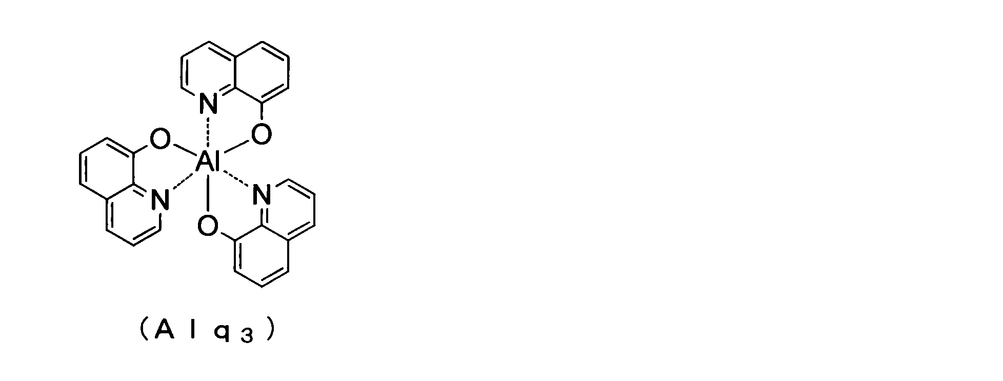
実施例14において、化合物群αを構成する化合物(H-A-3)及び化合物(H-A-41)を表3に示した化合物、組成に置き換えたほかは、実施例14と同様に組成物を調製し、一週間後、該組成物を用いて有機電界発光素子を作成した。この素子は電圧を印加することにより緑色に発光し、表3に示す特性を示した。
実施例14において、化合物群αを化合物(H-A-41)に置き換えたほかは、実施例14と同様に組成物を調製し、調液した当日に該組成物を用いて有機電界発光素子を作成した。この素子は電圧を印加することにより緑色に発光し、表3に示す特性を示した。

褐色サンプル瓶に、化合物群α(化合物(H-A-15)、化合物(H-A-48)の1:1混合物)、化合物(H-E-63)及び下記化合物(L-2)を含有する組成物を調製した。該組成物は、有機電界発光素子において赤色発光層用塗布液として用いることができる。該組成物を一週間保存した組成物を用い、実施例14にて示した方法にて有機電界発光素子を作製した。この素子は電圧を印加することにより赤色に発光し、表4に示す特性を示した。なお、H-E-63は、日本国特開2011-026237号公報にて開示されている方法にて調製し、L-2は以下の方法にて調製した。
溶媒 シクロヘキシルベンゼン
固形分濃度 化合物群α 1.2重量%
H-E-63 3.6重量%
L-2 0.48重量%

(中間体25の合成)


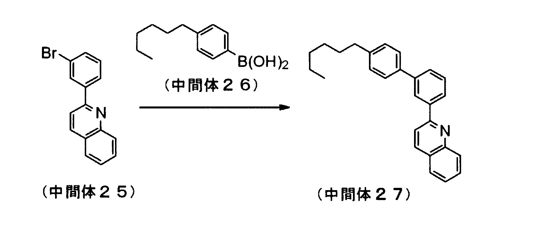


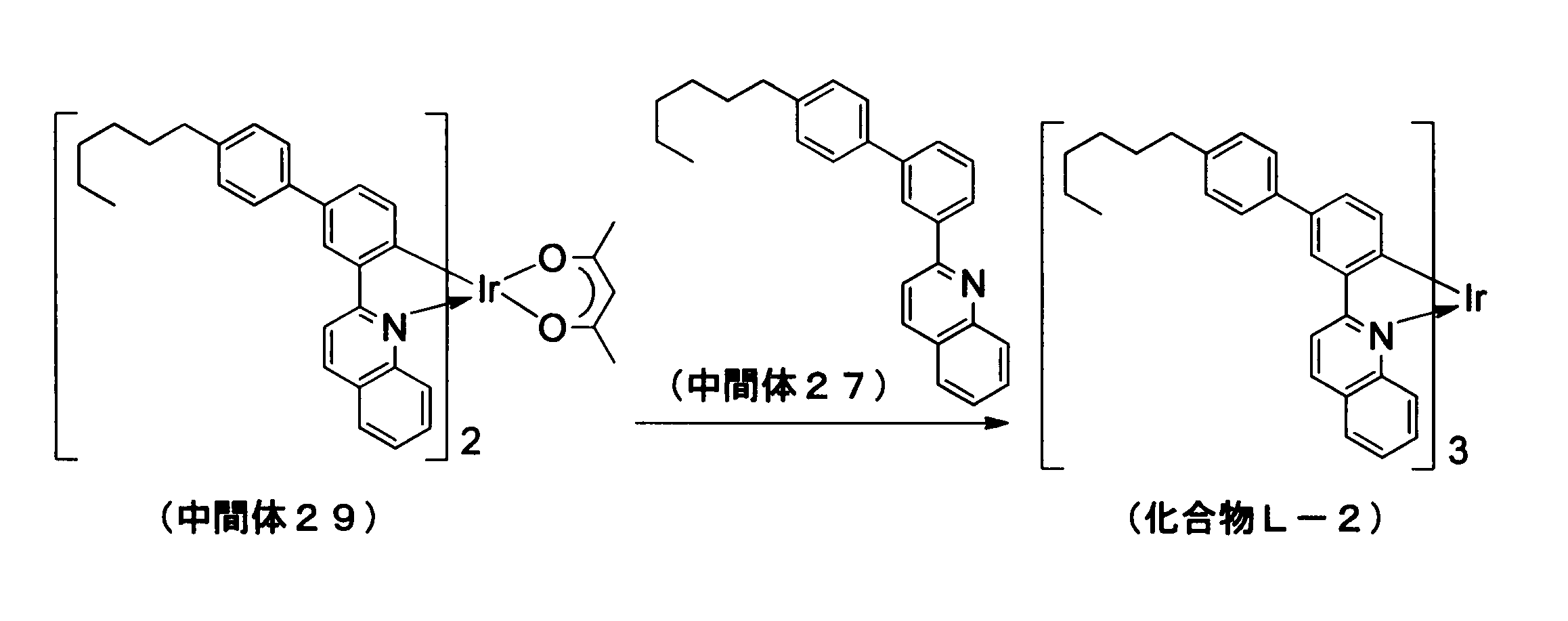
実施例17において、化合物群αを構成する化合物(H-A-15)及び化合物(H-A-48)を表4に示した化合物、組成に置き換えたほかは、実施例17と同様に組成物を調製し、一週間後、該組成物を用いて有機電界発光素子を作成した。この素子は電圧を印加することにより赤色に発光し、表4に示すような特性を示した。
実施例17において、化合物群αを化合物(H-A-15)に置き換えたほかは、実施例17と同様に組成物を調製し、調液した当日に該組成物を用いて有機電界発光素子を作成した。この素子は電圧を印加することにより赤色に発光し、表4に示す特性を示した。
実施例17において、化合物群αを化合物(H-A-15)と下記化合物(H-1)の1:1混合物としたほかは、実施例17と同様に組成物を調製し、一週間後、該組成物を用いて有機電界発光素子を作成した。この素子は電圧を印加することにより赤色に発光し、表4に示すような特性を示した。


褐色サンプル瓶に、化合物(H-B-14)を10.0mg、化合物(H-B-54)を20.0mg量りとり、ジエチルベンゼンを加えて860mgとした後、ホットプレートを用いて120℃に加熱し、化合物(H-B-14)及び化合物(H-B-54)を完全に溶解させ、化合物(H-B-14)と化合物(H-B-54)の1:2混合物(化合物群α)を含有する組成物(固形分濃度:3.5重量%)を調製した。このとき、両者の芳香環基の数は同じであるため、ここでは化合物(H-B-14)を化合物α1とした。調製した組成物は、室温約15~20℃の暗所に置き、固体が析出するまでの時間を測定した。固体は10倍のルーペを用いて目視にて確認を行い、その結果を表5にまとめた。
実施例19において化合物(H-B-14)及び化合物(H-B-54)を表5に示した化合物、組成、溶剤に置き換えたほかは、実施例19と同様に組成物を調製し、固体が析出するまでの時間を測定した。固体は10倍のルーペを用いて目視にて確認を行い、結果を表5にまとめた。
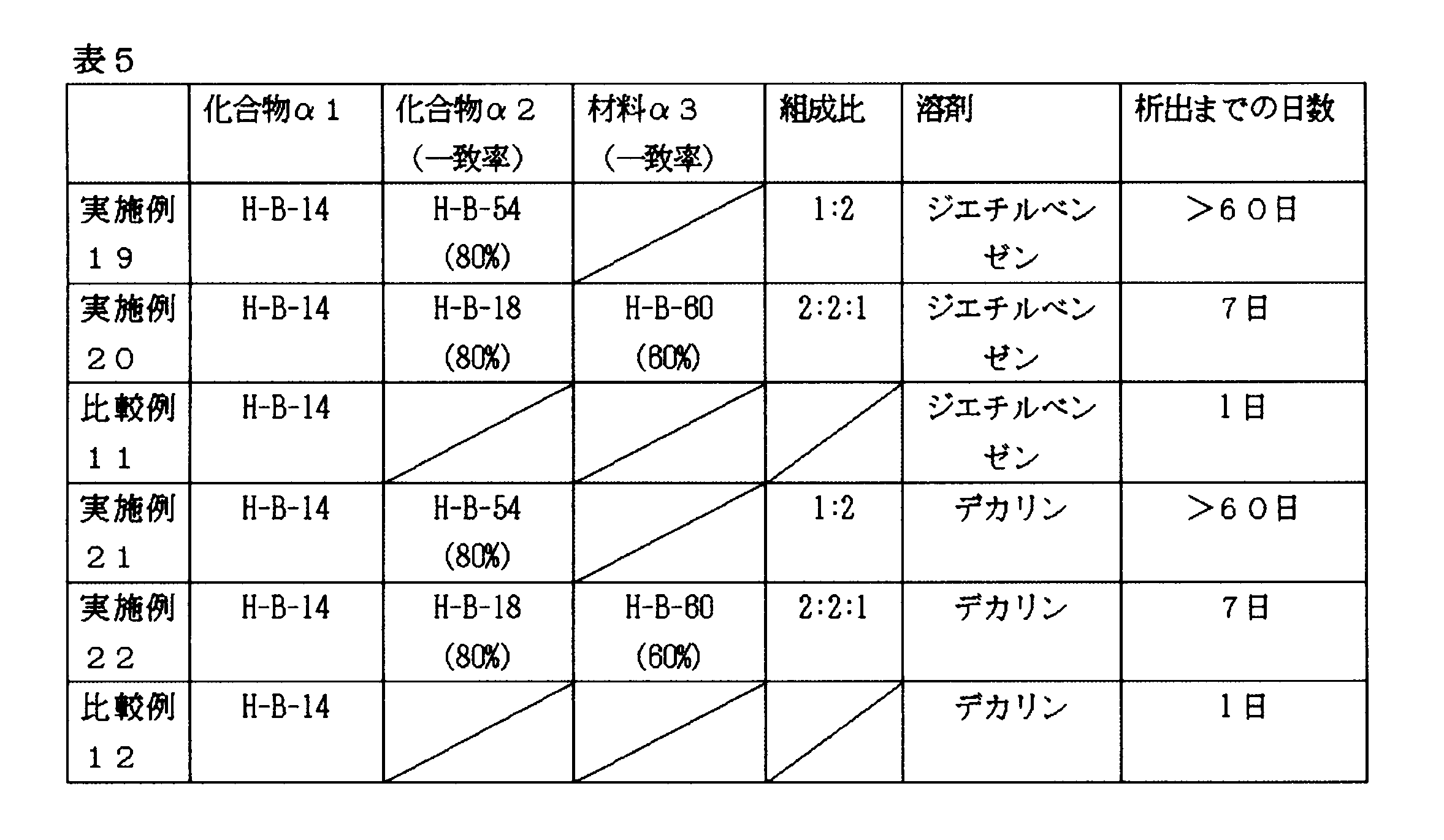
褐色サンプル瓶に、化合物群α(化合物(H-B-14)、化合物(H-B-54)の1:2混合物)及び化合物(L-C-2)を含有する組成物を調製した。該組成物は、有機電界発光素子において青色発光層用塗布液として用いることができる。該組成物を一週間保存した組成物を用い、実施例14にて示した方法にて有機電界発光素子を作製した。この際の発光層5の膜厚は45nmであった。この素子は電圧を印加することにより青色に発光し、表6に示す特性を示した。なお、L-C-2は、国際公開第2006/082705号にて開示されている方法にて調製した。
溶媒 シクロヘキシルベンゼン
固形分濃度 化合物群α 3.5重量%
L-C-2 0.35重量%
実施例23において、化合物群αを化合物(H-B-14)に置き換えたほかは、実施例23と同様に組成物を調製し、調液した当日に該組成物を用いて実施例23と同様に有機電界発光素子を作成した。この素子は電圧を印加することにより青色に発光し、表6に示す特性を示した。
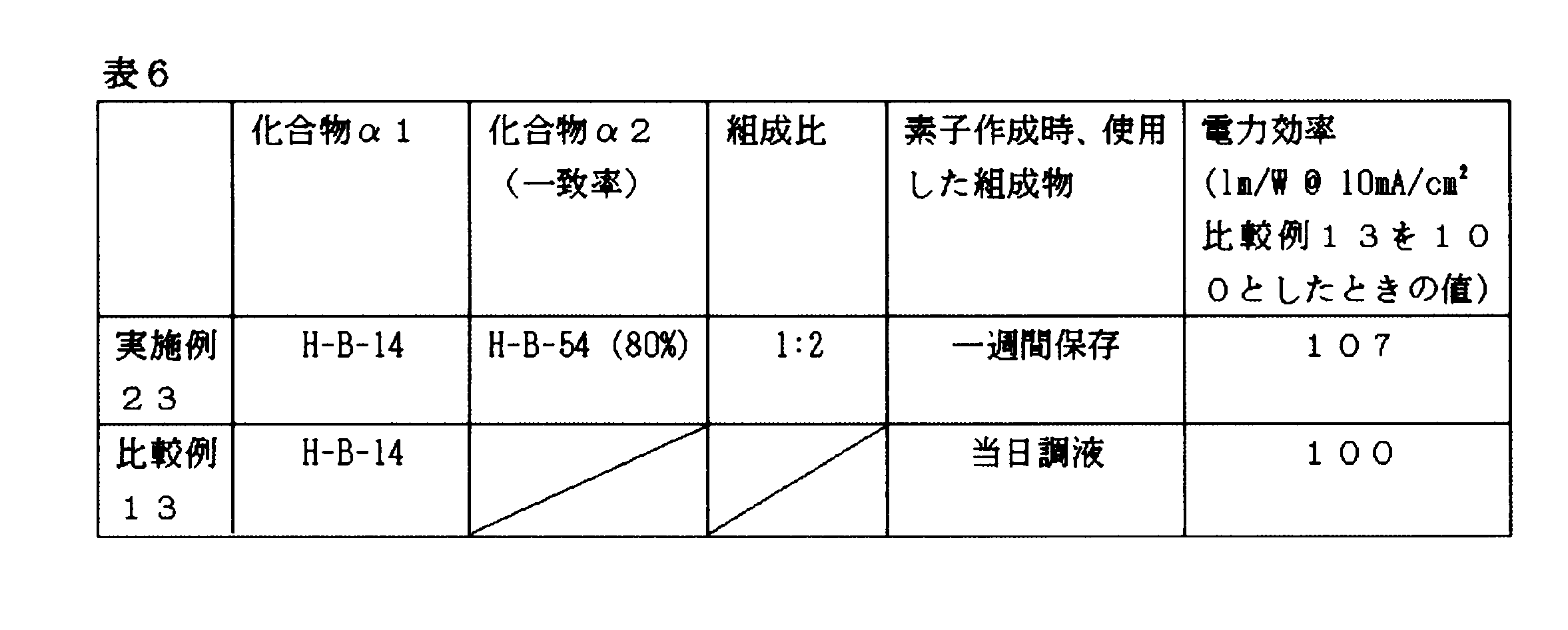
褐色サンプル瓶に、化合物(L-C-3)を1.5mg、化合物(L-C-7)を1.5mg量りとり、シクロへキシルベンゼンを加えて860mgとした後、ホットプレートを用いて120℃に加熱し、化合物(L-C-3)及び化合物(L-C-7)を完全に溶解させ、化合物(L-C-3)と化合物(L-C-7)の1:1混合物(化合物群α)を含有する組成物(固形分濃度:0.35重量%)を調製した。このとき、両者の芳香環基の数は同じであるため、ここでは化合物(L-C-3)を化合物α1とした。調製した組成物は、室温約15~20℃の暗所に置き、固体が析出するまでの時間を測定した。固体は10倍のルーペを用いて目視にて確認を行い、その結果を表7にまとめた。
実施例24において化合物群αを化合物(L-C-3)に置き換えたほかは、実施例24と同様に組成物を調製し、固体が析出するまでの時間を測定した。固体は10倍のルーペを用いて目視にて確認を行い、結果を表7にまとめた。
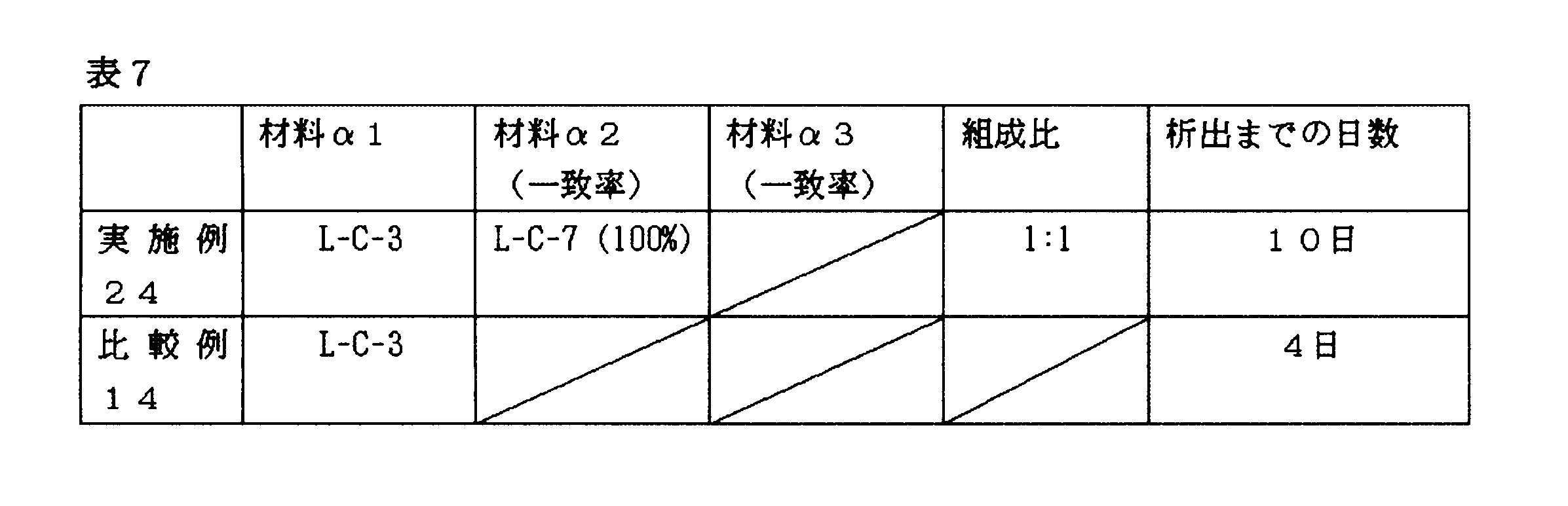
褐色サンプル瓶に、化合物群α(化合物(L-C-3)、化合物(L-C-7)の1:1混合物)及び化合物(H-B-52)を含有する組成物を調製した。該組成物は、有機電界発光素子において青色発光層用塗布液として用いることができる。該組成物を一週間保存した組成物を用い、実施例23にて示した方法にて有機電界発光素子を作製した。この素子は電圧を印加することにより青色に発光し、表8に示すような特性を示した。なお、H-B-52は、日本国特開2011-100942号公報にて開示されている方法にて調製した。
溶媒 シクロヘキシルベンゼン
固形分濃度 化合物群α 0.35重量%
H-B-52 3.5重量%
実施例25において、化合物群αを化合物(L-C-3)及び(L-C-10)に置き換えたほかは、実施例25と同様に組成物を調製し、一週間保存した後に、該組成物を用いて実施例25と同様に有機電界発光素子を作成した。この素子は電圧を印加することにより青色に発光し、表8に示すような特性を示した。
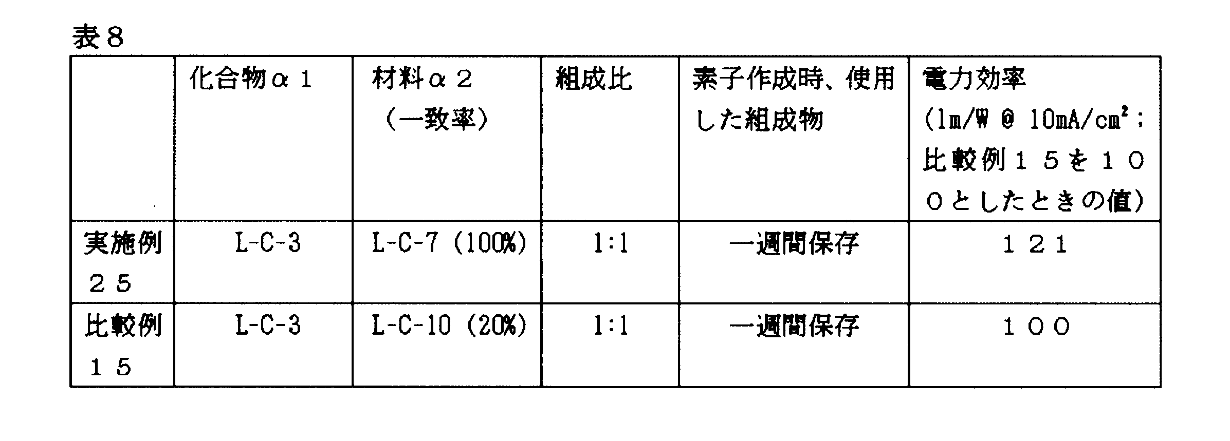
褐色サンプル瓶に、化合物(H-E-33)を15.0mg、化合物(H-E-42)を15.0mg量りとり、シクロへキシルベンゼンを加えて625mgとした後、ホットプレートを用いて120℃に加熱し、化合物(H-E-33)及び化合物(H-E-42)を完全に溶解させ、化合物(H-E-33)と化合物(H-E-42)の1:1混合物(化合物群α)を含有する組成物(固形分濃度:4.8重量%)を調製した。このとき、化合物(H-E-33)の芳香環基の数が少ないため、化合物(H-E-33)が化合物α1となる。調製した組成物は、室温約15~20℃の暗所に置き、固体が析出するまでの時間を測定した。固体は10倍のルーペを用いて目視にて確認を行い、その結果を表9にまとめた。
実施例26において化合物群αを表9に示す化合物及び組成に置き換えたほかは、実施例26と同様に組成物を調製し、固体が析出するまでの時間を測定した。固体は10倍のルーペを用いて目視にて確認を行い、結果を表9にまとめた。なお、この表に掲げた化合物は、以下のいずれかの文献にて開示されている方法にて調製した。;日本国特開2006-352088号公報,日本国特開2007-110093号公報,日本国特開2010-206191号公報,日本国特開2011-51936号公報,日本国特開2011-26237号公報

褐色サンプル瓶に、化合物群α(化合物(H-E-33)、化合物(H-E-22)、化合物(H-E-77)の1:1:2混合物)、化合物(H-E-23)及び化合物(L-1)を含有する組成物を調製した。該組成物は、有機電界発光素子において緑色発光層用塗布液として用いることができる。該組成物を一週間保存した組成物を用い、実施例14にて示した方法にて有機電界発光素子を作製した。この素子は電圧を印加することにより緑色に発光し、表10に示す特性を示した。
溶媒 シクロヘキシルベンゼン
固形分濃度 化合物群α 3.6重量%
H-A-11 1.2重量%
L-1 0.48重量%
実施例34において、化合物群αを、化合物(H-E-43)及び化合物(H-E-77)の1:1混合物に置き換えたほかは、実施例34と同様に組成物を調製し、一週間後、該組成物を用いて有機電界発光素子を作成した。この素子は電圧を印加することにより緑色に発光し、表10に示す特性を示した。
実施例34において、化合物群αを表10に示す化合物に置き換えたほかは、実施例34と同様に組成物を調製し、調液した当日に該組成物を用いて有機電界発光素子を作成した。この素子は電圧を印加することにより緑色に発光し、表10に示す特性を示した。
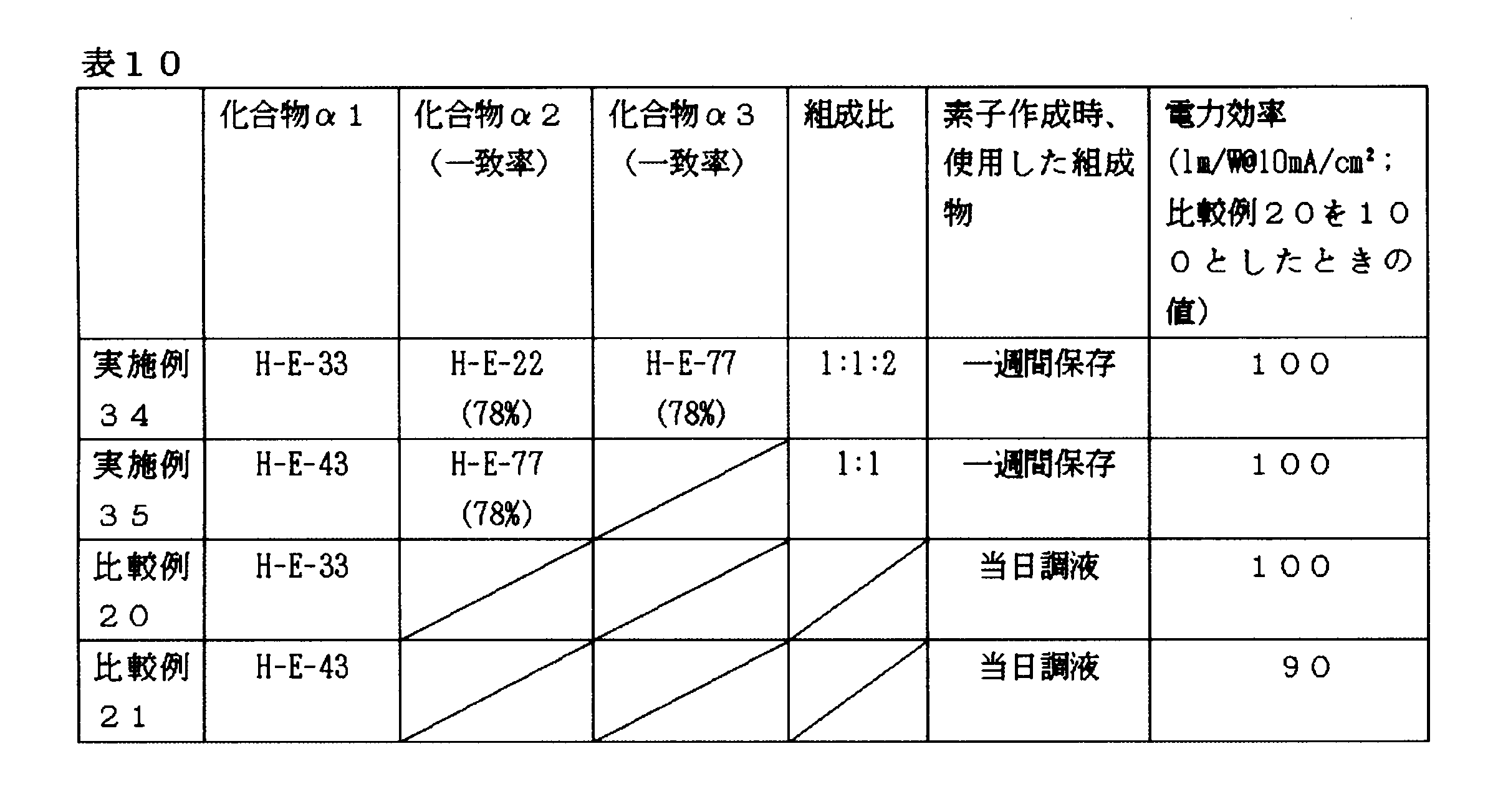
2 陽極
3 正孔注入層
4 正孔輸送層
5 発光層
6 正孔阻止層
7 電子輸送層
8 電子注入層
9 陰極
Claims (17)
- 有機電界発光素子用化合物群αおよび溶剤を含む、有機電界発光素子用組成物であって、
前記化合物群αは、複数の芳香環基が連結した構造を有する、分子量3000以下である、少なくとも2種以上の化合物から構成され、
前記化合物群αは、最も芳香環基の数が少ない化合物をα1、および他の化合物αn(nは、2以上の任意の整数)からなり、化合物α1と化合物αnの共通する部分構造のうち、最も芳香環基数が多い構造を基本骨格とした場合、
化合物α1の構造は、基本骨格と60%以上一致しており、
且つ化合物群αを構成する各々の化合物がそれぞれ1重量%以上混合されている、有機電界発光素子用組成物。 - 前記組成物中の全固形分に対する、前記化合物群αの割合が0.1~100重量%である、請求項1記載の有機電界発光素子用組成物。
- 前記組成物中の溶剤の割合が10重量%以上である、請求項1又は請求項2記載の有機電界発光素子用組成物。
- 前記化合物群αに含まれる化合物がいずれも電荷輸送材料である、請求項1~請求項3のいずれか一項に記載の有機電界発光素子用組成物。
- 前記化合物群αに含まれる化合物が、いずれも下記一般式(A)で表される化合物である、請求項1~請求項4のいずれか一項に記載の有機電界発光素子用組成物。

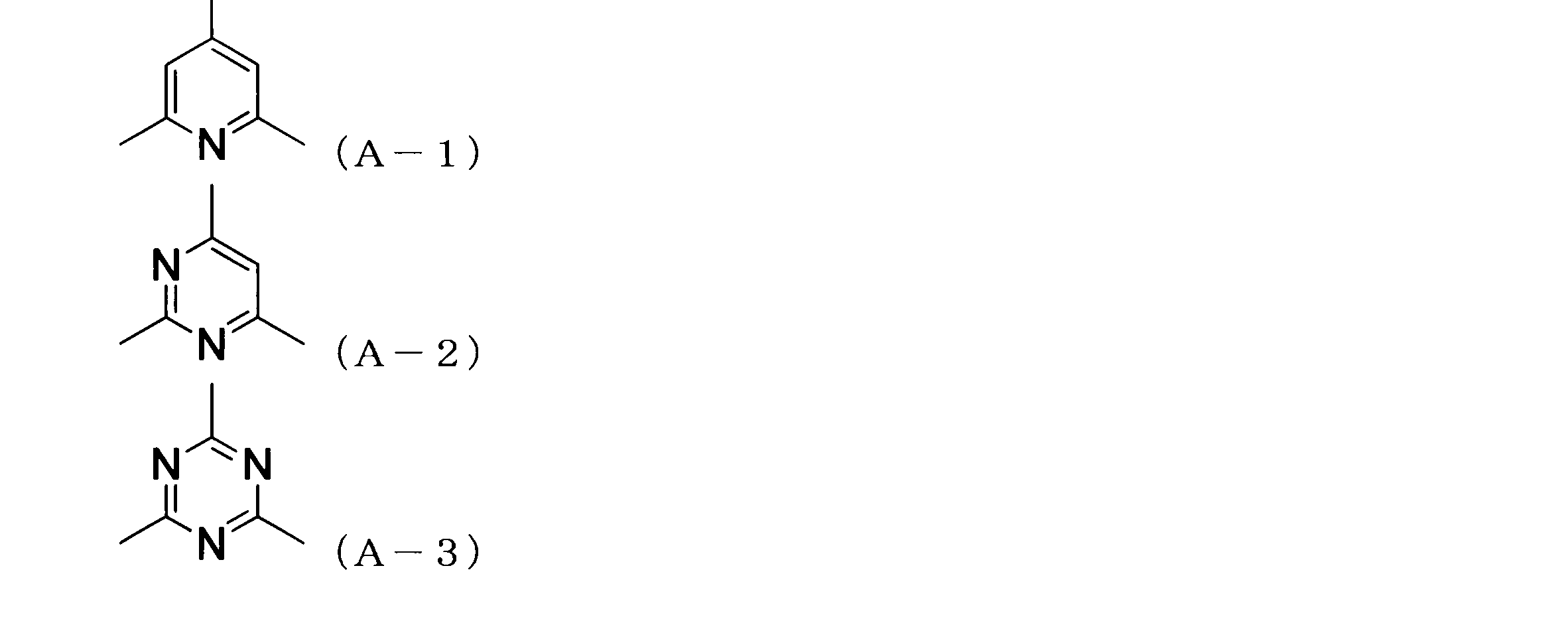
- 前記一般式(A)で表される化合物が、下記一般式(A-4)、(A-5)及び(A-6)で表される化合物のいずれかである、請求項5記載の有機電界発光素子用組成物。

- 前記一般式(A)で表される化合物が、前記一般式(A-4)、(A-5)及び(A-6)からなる群から選ばれるいずれか2種類のみで表される、請求項5記載の有機電界発光素子用組成物。
- 前記一般式(A)で表される化合物が、前記一般式(A-4)、(A-5)及び(A-6)からなる群から選ばれるいずれか1種類のみで表される、請求項5記載の有機電界発光素子用組成物。
- 前記化合物群αに含まれる化合物が、いずれも下記一般式(B)で表される化合物である、請求項1~請求項4のいずれか一項に記載の有機電界発光素子用組成物。

- 前記化合物群αに含まれる材料が、いずれも下記一般式(C)で表される化合物である、請求項1~請求項4のいずれか一項に記載の有機電界発光素子用組成物。

- 前記化合物群αに含まれる化合物が、いずれも下記一般式(D)で表される化合物である、請求項1~請求項4のいずれか一項に記載の有機電界発光素子用組成物。
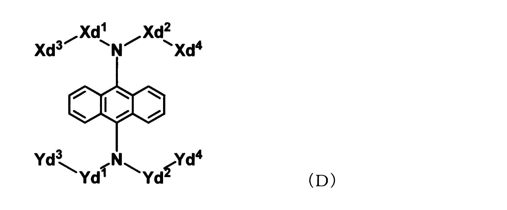
- 前記化合物群αに含まれる化合物が、いずれも下記一般式(E)で表される化合物である、請求項1~請求項4のいずれか一項に記載の有機電界発光素子用組成物。

- 前記一般式(E)で表される化合物が、下記一般式(E-1)で表わされる化合物である、請求項12に記載の有機電界発光素子用組成物。
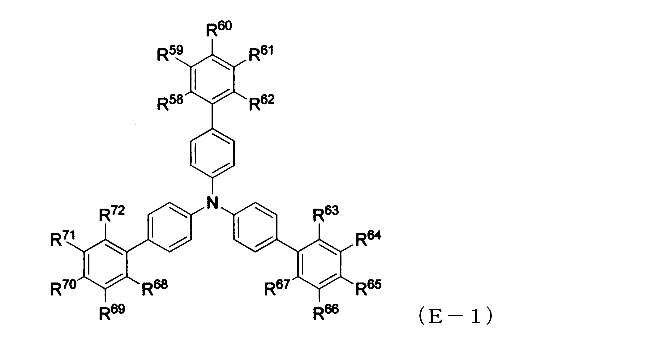
- 陽極、陰極、及びこれらの間に少なくとも1層の有機層を有する有機電界発光素子であり、該有機層のうち少なくとも1層が、請求項1~請求項13のいずれか一項に記載の有機電界発光素子用組成物を用いて形成された層である、有機電界発光素子。
- 請求項1~請求項13のいずれか一項に記載の有機電界発光素子用組成物を用いて形成された層が発光層である、請求項14に記載の有機電界発光素子。
- 請求項14又は請求項15に記載の有機電界発光素子を有する表示装置。
- 請求項14又は請求項15に記載の有機電界発光素子を有する照明装置。
Priority Applications (8)
| Application Number | Priority Date | Filing Date | Title |
|---|---|---|---|
| EP12734183.2A EP2665342B1 (en) | 2011-01-11 | 2012-01-10 | Composition for organic electroluminescent element, organic electroluminescent element, display device, and illuminator |
| JP2012537043A JP5163837B2 (ja) | 2011-01-11 | 2012-01-10 | 有機電界発光素子用組成物、有機電界発光素子、表示装置及び照明装置 |
| KR1020197014532A KR102042468B1 (ko) | 2011-01-11 | 2012-01-10 | 유기 전계 발광 소자용 조성물, 유기 전계 발광 소자, 표시 장치 및 조명 장치 |
| KR1020137018072A KR101983401B1 (ko) | 2011-01-11 | 2012-01-10 | 유기 전계 발광 소자용 조성물, 유기 전계 발광 소자, 표시 장치 및 조명 장치 |
| CN201280005151.5A CN103329619B (zh) | 2011-01-11 | 2012-01-10 | 有机电致发光器件用组合物、有机电致发光器件、显示装置及照明装置 |
| KR1020197032469A KR102101248B1 (ko) | 2011-01-11 | 2012-01-10 | 유기 전계 발광 소자용 조성물, 유기 전계 발광 소자, 표시 장치 및 조명 장치 |
| US13/939,881 US9899606B2 (en) | 2011-01-11 | 2013-07-11 | Composition for organic electroluminescent element, organic electroluminescent element, display and lighting |
| US15/856,708 US20180123054A1 (en) | 2011-01-11 | 2017-12-28 | Composition for organic electroluminescent element, organic electroluminescent element, display and lighting |
Applications Claiming Priority (2)
| Application Number | Priority Date | Filing Date | Title |
|---|---|---|---|
| JP2011-003081 | 2011-01-11 | ||
| JP2011003081 | 2011-01-11 |
Related Child Applications (1)
| Application Number | Title | Priority Date | Filing Date |
|---|---|---|---|
| US13/939,881 Continuation US9899606B2 (en) | 2011-01-11 | 2013-07-11 | Composition for organic electroluminescent element, organic electroluminescent element, display and lighting |
Publications (1)
| Publication Number | Publication Date |
|---|---|
| WO2012096263A1 true WO2012096263A1 (ja) | 2012-07-19 |
Family
ID=46507161
Family Applications (1)
| Application Number | Title | Priority Date | Filing Date |
|---|---|---|---|
| PCT/JP2012/050288 WO2012096263A1 (ja) | 2011-01-11 | 2012-01-10 | 有機電界発光素子用組成物、有機電界発光素子、表示装置及び照明装置 |
Country Status (7)
| Country | Link |
|---|---|
| US (2) | US9899606B2 (ja) |
| EP (1) | EP2665342B1 (ja) |
| JP (1) | JP5163837B2 (ja) |
| KR (3) | KR102101248B1 (ja) |
| CN (1) | CN103329619B (ja) |
| TW (1) | TWI484019B (ja) |
| WO (1) | WO2012096263A1 (ja) |
Cited By (25)
| Publication number | Priority date | Publication date | Assignee | Title |
|---|---|---|---|---|
| WO2013027846A1 (en) * | 2011-08-25 | 2013-02-28 | Semiconductor Energy Laboratory Co., Ltd. | Light-emitting element, light-emitting device, electronic device, lighting device, and novel organic compound |
| WO2013105615A1 (ja) | 2012-01-13 | 2013-07-18 | 三菱化学株式会社 | イリジウム錯体化合物並びに該化合物を含む溶液組成物、有機電界発光素子、表示装置及び照明装置 |
| WO2014021441A1 (en) * | 2012-08-03 | 2014-02-06 | Semiconductor Energy Laboratory Co., Ltd. | Light-emitting element, light-emitting device, electronic device, and lighting device |
| WO2014200260A1 (en) * | 2013-06-13 | 2014-12-18 | Sk Chemicals Co., Ltd. | Compound for organic electroluminescent device and organic electroluminescent device including the same |
| US9059411B2 (en) | 2012-02-29 | 2015-06-16 | Semiconductor Energy Laboratory Co., Ltd. | Fluorene compound, light-emitting element, light-emitting device, electronic device, and lighting device |
| WO2015087961A1 (ja) | 2013-12-12 | 2015-06-18 | 三菱化学株式会社 | イリジウム錯体化合物、該化合物の製造方法、該化合物を含む組成物、有機電界発光素子、表示装置及び照明装置 |
| US9412953B2 (en) | 2012-08-03 | 2016-08-09 | Semiconductor Energy Laboratory Co., Ltd. | Light-emitting element, light-emitting device, electronic device, lighting device, and heterocyclic compound |
| JP2016204366A (ja) * | 2015-04-14 | 2016-12-08 | 株式会社半導体エネルギー研究所 | 複素環化合物、発光素子、発光装置、電子機器、および照明装置 |
| WO2017154883A1 (ja) * | 2016-03-10 | 2017-09-14 | 住友化学株式会社 | 発光素子 |
| WO2017170313A1 (ja) | 2016-03-29 | 2017-10-05 | 住友化学株式会社 | 発光素子 |
| WO2017221822A1 (ja) | 2016-06-24 | 2017-12-28 | 住友化学株式会社 | 発光素子 |
| JPWO2017154882A1 (ja) * | 2016-03-10 | 2018-03-15 | 住友化学株式会社 | 発光素子 |
| US9923149B2 (en) | 2014-05-23 | 2018-03-20 | Semiconductor Energy Laboratory Co., Ltd. | Heterocyclic compound, light-emitting element, light-emitting device, electronic device, and lighting device |
| WO2018062277A1 (ja) * | 2016-09-29 | 2018-04-05 | 住友化学株式会社 | 発光素子 |
| WO2018062278A1 (ja) | 2016-09-29 | 2018-04-05 | 住友化学株式会社 | 発光素子及び該発光素子の製造に有用な組成物 |
| US10014477B2 (en) | 2012-08-31 | 2018-07-03 | Idemitsu Kosan Co., Ltd. | Aromatic amine derivative, and organic electroluminescent element using same |
| US10147886B2 (en) | 2014-10-06 | 2018-12-04 | Samsung Display Co., Ltd. | Organic electroluminescent material and organic electroluminescent device including the same |
| WO2019049225A1 (ja) | 2017-09-06 | 2019-03-14 | 住友化学株式会社 | 発光素子 |
| WO2019054341A1 (ja) | 2017-09-14 | 2019-03-21 | 住友化学株式会社 | 液状組成物の製造方法 |
| US10497885B2 (en) | 2015-04-24 | 2019-12-03 | Sumitomo Chemical Company, Limited | Light emitting device and composition used for this light emitting device |
| WO2019239998A1 (ja) | 2018-06-12 | 2019-12-19 | 住友化学株式会社 | 有機エレクトロルミネッセンス素子 |
| WO2021060239A1 (ja) * | 2019-09-26 | 2021-04-01 | 出光興産株式会社 | 化合物、有機エレクトロルミネッセンス素子用材料、有機エレクトロルミネッセンス素子及び電子機器 |
| WO2021161974A1 (ja) * | 2020-02-12 | 2021-08-19 | 三菱ケミカル株式会社 | イリジウム錯体化合物、イリジウム錯体化合物含有組成物、有機電界発光素子とその製造方法、有機el表示装置、及び有機el照明装置 |
| WO2022024664A1 (ja) | 2020-07-28 | 2022-02-03 | 住友化学株式会社 | 組成物及び発光素子 |
| KR20240016964A (ko) | 2021-06-04 | 2024-02-06 | 미쯔비시 케미컬 주식회사 | 화합물 및 유기 전계 발광 소자 |
Families Citing this family (17)
| Publication number | Priority date | Publication date | Assignee | Title |
|---|---|---|---|---|
| TWI593151B (zh) * | 2011-11-11 | 2017-07-21 | 三菱化學股份有限公司 | 有機電致發光元件及有機電致發光裝置 |
| CN107501244B (zh) | 2011-11-22 | 2022-05-03 | 出光兴产株式会社 | 芳香族杂环衍生物、有机电致发光元件用材料以及有机电致发光元件 |
| JP5594750B2 (ja) * | 2012-05-17 | 2014-09-24 | 国立大学法人九州大学 | 化合物、発光材料および有機発光素子 |
| US9312500B2 (en) | 2012-08-31 | 2016-04-12 | Idemitsu Kosan Co., Ltd. | Organic electroluminescence device |
| EP2924029B1 (en) | 2013-03-15 | 2018-12-12 | Idemitsu Kosan Co., Ltd | Anthracene derivative and organic electroluminescence element using same |
| JP6136890B2 (ja) * | 2013-11-26 | 2017-05-31 | ソニー株式会社 | 表示装置、表示装置の製造方法および電子機器 |
| JP6425395B2 (ja) * | 2014-03-14 | 2018-11-21 | 出光興産株式会社 | インク組成物、インク組成物を用いた有機エレクトロルミネッセンス素子、及び電子機器 |
| JP6468800B2 (ja) | 2014-10-29 | 2019-02-13 | 三星ディスプレイ株式會社Samsung Display Co.,Ltd. | アミン誘導体、有機エレクトロルミネッセンス素子用材料及びそれを用いた有機エレクトロルミネッセンス素子 |
| TWI697485B (zh) | 2015-07-21 | 2020-07-01 | 日商捷恩智股份有限公司 | 含唑啉環的化合物、含有其的電子輸送/注入層用材料、使用其的有機電致發光元件、顯示裝置及照明裝置 |
| JP6740560B2 (ja) | 2017-03-09 | 2020-08-19 | エルジー・ケム・リミテッド | 有機発光素子 |
| KR20230117645A (ko) | 2017-04-26 | 2023-08-08 | 오티아이 루미오닉스 인크. | 표면의 코팅을 패턴화하는 방법 및 패턴화된 코팅을포함하는 장치 |
| KR102064645B1 (ko) * | 2017-06-08 | 2020-01-09 | 주식회사 엘지화학 | 유기 발광 소자 |
| CN111655674B (zh) | 2018-01-29 | 2024-01-23 | 出光兴产株式会社 | 化合物和使用该化合物的有机电致发光元件 |
| US11751415B2 (en) | 2018-02-02 | 2023-09-05 | Oti Lumionics Inc. | Materials for forming a nucleation-inhibiting coating and devices incorporating same |
| KR20190140233A (ko) | 2018-06-11 | 2019-12-19 | 엘지디스플레이 주식회사 | 유기발광 화합물 및 이를 포함하는 유기발광소자 |
| CN113785411B (zh) | 2019-03-07 | 2023-04-11 | Oti照明公司 | 用于形成成核抑制涂层的材料和结合所述成核抑制涂层的装置 |
| CN111087387B (zh) | 2019-12-26 | 2022-04-29 | 厦门天马微电子有限公司 | 一种有机化合物、显示面板及显示装置 |
Citations (6)
| Publication number | Priority date | Publication date | Assignee | Title |
|---|---|---|---|---|
| JP2009141339A (ja) * | 2007-11-15 | 2009-06-25 | Mitsubishi Chemicals Corp | 有機電界発光素子用組成物および有機電界発光素子 |
| JP2010087488A (ja) * | 2008-09-04 | 2010-04-15 | Mitsubishi Chemicals Corp | 有機電界発光素子材料、有機電界発光素子用組成物、有機電界発光素子、有機elディスプレイ、有機el照明およびナフタレン系化合物 |
| JP2010183072A (ja) * | 2009-01-09 | 2010-08-19 | Mitsubishi Chemicals Corp | 有機el素子及び有機発光デバイス |
| JP2010206191A (ja) * | 2009-02-09 | 2010-09-16 | Mitsubishi Chemicals Corp | 有機電界発光素子材料、湿式成膜用有機電界発光素子用組成物および有機電界発光素子 |
| JP2011026237A (ja) * | 2009-07-24 | 2011-02-10 | Mitsubishi Chemicals Corp | 有機化合物、電荷輸送材料、有機電界発光素子用組成物、有機電界発光素子、有機elディスプレイ及び有機el照明 |
| JP2011051936A (ja) * | 2009-09-02 | 2011-03-17 | Mitsubishi Chemicals Corp | 有機化合物、電荷輸送材料、有機電界発光素子用組成物、有機電界発光素子、有機elディスプレイ及び有機el照明 |
Family Cites Families (14)
| Publication number | Priority date | Publication date | Assignee | Title |
|---|---|---|---|---|
| KR100577179B1 (ko) * | 2001-10-30 | 2006-05-10 | 엘지전자 주식회사 | 유기 전계 발광 소자 |
| JP4106974B2 (ja) * | 2002-06-17 | 2008-06-25 | コニカミノルタホールディングス株式会社 | 有機エレクトロルミネッセンス素子及び表示装置 |
| US7045952B2 (en) * | 2004-03-04 | 2006-05-16 | Universal Display Corporation | OLEDs with mixed host emissive layer |
| TWI373506B (en) * | 2004-05-21 | 2012-10-01 | Toray Industries | Light-emitting element material and light-emitting material |
| TWI290582B (en) * | 2004-07-06 | 2007-12-01 | Au Optronics Corp | Anthracene compound and organic electroluminescent device including the anthracene compound |
| WO2006008976A1 (ja) | 2004-07-16 | 2006-01-26 | Konica Minolta Holdings, Inc. | 白色発光有機エレクトロルミネッセンス素子、表示装置及び照明装置 |
| GB2438771B (en) | 2005-03-02 | 2011-01-26 | Konica Minolta Holdings Inc | Organic electroluminescence element, image display unit and lighting device |
| TWI418606B (zh) * | 2005-04-25 | 2013-12-11 | Udc Ireland Ltd | 有機電致發光裝置 |
| JP4967864B2 (ja) | 2007-07-06 | 2012-07-04 | 三菱化学株式会社 | 有機電界発光素子 |
| US8877350B2 (en) * | 2007-12-11 | 2014-11-04 | Global Oled Technology Llc | White OLED with two blue light-emitting layers |
| JP2010150425A (ja) * | 2008-12-25 | 2010-07-08 | Idemitsu Kosan Co Ltd | 新規重合性単量体とその重合体、それを用いた有機デバイス用材料、及び有機エレクトロルミネッセンス素子 |
| US20120267612A1 (en) * | 2009-01-14 | 2012-10-25 | Universal Display Corporation | Cross-linkable copper phthalocyanine complexes |
| KR101596906B1 (ko) * | 2009-02-27 | 2016-03-07 | 신닛테츠 수미킨 가가쿠 가부시키가이샤 | 유기 전계 발광 소자 |
| KR101120892B1 (ko) | 2009-06-19 | 2012-02-27 | 주식회사 두산 | 아크리딘 유도체 및 이를 포함하는 유기 전계 발광 소자 |
-
2012
- 2012-01-10 KR KR1020197032469A patent/KR102101248B1/ko active IP Right Grant
- 2012-01-10 CN CN201280005151.5A patent/CN103329619B/zh active Active
- 2012-01-10 WO PCT/JP2012/050288 patent/WO2012096263A1/ja active Application Filing
- 2012-01-10 EP EP12734183.2A patent/EP2665342B1/en active Active
- 2012-01-10 KR KR1020137018072A patent/KR101983401B1/ko active IP Right Grant
- 2012-01-10 JP JP2012537043A patent/JP5163837B2/ja active Active
- 2012-01-10 KR KR1020197014532A patent/KR102042468B1/ko active IP Right Grant
- 2012-01-11 TW TW101101110A patent/TWI484019B/zh active
-
2013
- 2013-07-11 US US13/939,881 patent/US9899606B2/en active Active
-
2017
- 2017-12-28 US US15/856,708 patent/US20180123054A1/en active Pending
Patent Citations (6)
| Publication number | Priority date | Publication date | Assignee | Title |
|---|---|---|---|---|
| JP2009141339A (ja) * | 2007-11-15 | 2009-06-25 | Mitsubishi Chemicals Corp | 有機電界発光素子用組成物および有機電界発光素子 |
| JP2010087488A (ja) * | 2008-09-04 | 2010-04-15 | Mitsubishi Chemicals Corp | 有機電界発光素子材料、有機電界発光素子用組成物、有機電界発光素子、有機elディスプレイ、有機el照明およびナフタレン系化合物 |
| JP2010183072A (ja) * | 2009-01-09 | 2010-08-19 | Mitsubishi Chemicals Corp | 有機el素子及び有機発光デバイス |
| JP2010206191A (ja) * | 2009-02-09 | 2010-09-16 | Mitsubishi Chemicals Corp | 有機電界発光素子材料、湿式成膜用有機電界発光素子用組成物および有機電界発光素子 |
| JP2011026237A (ja) * | 2009-07-24 | 2011-02-10 | Mitsubishi Chemicals Corp | 有機化合物、電荷輸送材料、有機電界発光素子用組成物、有機電界発光素子、有機elディスプレイ及び有機el照明 |
| JP2011051936A (ja) * | 2009-09-02 | 2011-03-17 | Mitsubishi Chemicals Corp | 有機化合物、電荷輸送材料、有機電界発光素子用組成物、有機電界発光素子、有機elディスプレイ及び有機el照明 |
Non-Patent Citations (1)
| Title |
|---|
| See also references of EP2665342A4 * |
Cited By (53)
| Publication number | Priority date | Publication date | Assignee | Title |
|---|---|---|---|---|
| JP2016106119A (ja) * | 2011-08-25 | 2016-06-16 | 株式会社半導体エネルギー研究所 | 有機化合物 |
| US11773321B2 (en) | 2011-08-25 | 2023-10-03 | Semiconductor Energy Laboratory Co., Ltd. | Light-emitting element, light-emitting device, electronic device, lighting device, and novel organic compound |
| US11008510B2 (en) | 2011-08-25 | 2021-05-18 | Semiconductor Energy Laboratory Co., Ltd. | Light-emitting element, light-emitting device, electronic device, lighting device, and novel organic compound |
| WO2013027846A1 (en) * | 2011-08-25 | 2013-02-28 | Semiconductor Energy Laboratory Co., Ltd. | Light-emitting element, light-emitting device, electronic device, lighting device, and novel organic compound |
| US9663711B2 (en) | 2011-08-25 | 2017-05-30 | Semiconductor Energy Laboratory Co., Ltd. | Light-emitting element, light-emitting device, electronic device, lighting device, and novel organic compound |
| JP2017041648A (ja) * | 2011-08-25 | 2017-02-23 | 株式会社半導体エネルギー研究所 | 発光素子、発光装置、電子機器、照明装置 |
| WO2013105615A1 (ja) | 2012-01-13 | 2013-07-18 | 三菱化学株式会社 | イリジウム錯体化合物並びに該化合物を含む溶液組成物、有機電界発光素子、表示装置及び照明装置 |
| US9059411B2 (en) | 2012-02-29 | 2015-06-16 | Semiconductor Energy Laboratory Co., Ltd. | Fluorene compound, light-emitting element, light-emitting device, electronic device, and lighting device |
| US10069076B2 (en) | 2012-08-03 | 2018-09-04 | Semiconductor Energy Laboratory Co., Ltd. | Light-emitting element, light-emitting device, electronic device, and lighting device |
| US10897012B2 (en) | 2012-08-03 | 2021-01-19 | Semiconductor Energy Laboratory Co., Ltd. | Light-emitting element, light-emitting device, electronic device, and lighting device |
| US9412953B2 (en) | 2012-08-03 | 2016-08-09 | Semiconductor Energy Laboratory Co., Ltd. | Light-emitting element, light-emitting device, electronic device, lighting device, and heterocyclic compound |
| US9412962B2 (en) | 2012-08-03 | 2016-08-09 | Semiconductor Energy Laboratory Co., Ltd. | Light-emitting element, light-emitting device, electronic device, and lighting device |
| US11968889B2 (en) | 2012-08-03 | 2024-04-23 | Semiconductor Energy Laboratory Co., Ltd. | Light-emitting element, light-emitting device, electronic device, and lighting device |
| WO2014021441A1 (en) * | 2012-08-03 | 2014-02-06 | Semiconductor Energy Laboratory Co., Ltd. | Light-emitting element, light-emitting device, electronic device, and lighting device |
| CN107068913A (zh) * | 2012-08-03 | 2017-08-18 | 株式会社半导体能源研究所 | 发光元件、发光装置、电子设备以及照明装置 |
| US10020451B2 (en) | 2012-08-03 | 2018-07-10 | Semiconductor Energy Laboratory Co., Ltd. | Light-emitting element, light-emitting device, electronic device, lighting device, and heterocyclic compound |
| US11043637B2 (en) | 2012-08-03 | 2021-06-22 | Semiconductor Energy Laboratory Co., Ltd. | Light-emitting element, light-emitting device, electronic device, and lighting device |
| JP2014197657A (ja) * | 2012-08-03 | 2014-10-16 | 株式会社半導体エネルギー研究所 | 発光素子、発光装置、電子機器、及び照明装置 |
| JP2018085524A (ja) * | 2012-08-03 | 2018-05-31 | 株式会社半導体エネルギー研究所 | 発光素子、発光装置、電子機器、および照明装置 |
| JP2020017751A (ja) * | 2012-08-03 | 2020-01-30 | 株式会社半導体エネルギー研究所 | 発光素子、発光装置、電子機器、及び照明装置 |
| US11444246B2 (en) | 2012-08-31 | 2022-09-13 | Idemitsu Kosan Co., Ltd. | Aromatic amine derivative, and organic electroluminescent element using same |
| US10014477B2 (en) | 2012-08-31 | 2018-07-03 | Idemitsu Kosan Co., Ltd. | Aromatic amine derivative, and organic electroluminescent element using same |
| US11362279B2 (en) | 2012-08-31 | 2022-06-14 | Idemitsu Kosan Co., Ltd. | Aromatic amine derivative, and organic electroluminescent element using same |
| WO2014200260A1 (en) * | 2013-06-13 | 2014-12-18 | Sk Chemicals Co., Ltd. | Compound for organic electroluminescent device and organic electroluminescent device including the same |
| CN105283525A (zh) * | 2013-06-13 | 2016-01-27 | Sk化学株式会社 | 用于有机电致发光器件的化合物以及含有该化合物的有机电致发光器件 |
| WO2015087961A1 (ja) | 2013-12-12 | 2015-06-18 | 三菱化学株式会社 | イリジウム錯体化合物、該化合物の製造方法、該化合物を含む組成物、有機電界発光素子、表示装置及び照明装置 |
| US9923149B2 (en) | 2014-05-23 | 2018-03-20 | Semiconductor Energy Laboratory Co., Ltd. | Heterocyclic compound, light-emitting element, light-emitting device, electronic device, and lighting device |
| US10770660B2 (en) | 2014-05-23 | 2020-09-08 | Semiconductor Energy Laboratory Co., Ltd. | Heterocyclic compound, light-emitting element, light-emitting device, electronic device, and lighting device |
| US10147886B2 (en) | 2014-10-06 | 2018-12-04 | Samsung Display Co., Ltd. | Organic electroluminescent material and organic electroluminescent device including the same |
| JP2016204366A (ja) * | 2015-04-14 | 2016-12-08 | 株式会社半導体エネルギー研究所 | 複素環化合物、発光素子、発光装置、電子機器、および照明装置 |
| US10497885B2 (en) | 2015-04-24 | 2019-12-03 | Sumitomo Chemical Company, Limited | Light emitting device and composition used for this light emitting device |
| JP2018157207A (ja) * | 2016-03-10 | 2018-10-04 | 住友化学株式会社 | 発光素子 |
| JPWO2017154882A1 (ja) * | 2016-03-10 | 2018-03-15 | 住友化学株式会社 | 発光素子 |
| JPWO2017154883A1 (ja) * | 2016-03-10 | 2018-03-15 | 住友化学株式会社 | 発光素子 |
| WO2017154883A1 (ja) * | 2016-03-10 | 2017-09-14 | 住友化学株式会社 | 発光素子 |
| WO2017170313A1 (ja) | 2016-03-29 | 2017-10-05 | 住友化学株式会社 | 発光素子 |
| WO2017221822A1 (ja) | 2016-06-24 | 2017-12-28 | 住友化学株式会社 | 発光素子 |
| JPWO2018062277A1 (ja) * | 2016-09-29 | 2018-10-04 | 住友化学株式会社 | 発光素子 |
| US11271166B2 (en) | 2016-09-29 | 2022-03-08 | Sumitomo Chemical Company, Limited | Light emitting device and composition useful for production of same light emitting device |
| JP6399248B2 (ja) * | 2016-09-29 | 2018-10-03 | 住友化学株式会社 | 発光素子 |
| WO2018062278A1 (ja) | 2016-09-29 | 2018-04-05 | 住友化学株式会社 | 発光素子及び該発光素子の製造に有用な組成物 |
| WO2018062277A1 (ja) * | 2016-09-29 | 2018-04-05 | 住友化学株式会社 | 発光素子 |
| WO2019049225A1 (ja) | 2017-09-06 | 2019-03-14 | 住友化学株式会社 | 発光素子 |
| US11515477B2 (en) | 2017-09-06 | 2022-11-29 | Sumitomo Chemical Company, Limited | Light emitting device having thermally activated delayed fluorescent (TADF) compound |
| US11046886B2 (en) | 2017-09-14 | 2021-06-29 | Sumitomo Chemical Company, Limited | Method for producing liquid composition |
| WO2019054341A1 (ja) | 2017-09-14 | 2019-03-21 | 住友化学株式会社 | 液状組成物の製造方法 |
| WO2019239998A1 (ja) | 2018-06-12 | 2019-12-19 | 住友化学株式会社 | 有機エレクトロルミネッセンス素子 |
| CN114423733A (zh) * | 2019-09-26 | 2022-04-29 | 出光兴产株式会社 | 化合物、有机电致发光元件用材料、有机电致发光元件和电子设备 |
| WO2021060239A1 (ja) * | 2019-09-26 | 2021-04-01 | 出光興産株式会社 | 化合物、有機エレクトロルミネッセンス素子用材料、有機エレクトロルミネッセンス素子及び電子機器 |
| WO2021161974A1 (ja) * | 2020-02-12 | 2021-08-19 | 三菱ケミカル株式会社 | イリジウム錯体化合物、イリジウム錯体化合物含有組成物、有機電界発光素子とその製造方法、有機el表示装置、及び有機el照明装置 |
| EP4105222A4 (en) * | 2020-02-12 | 2023-07-19 | Mitsubishi Chemical Corporation | COMPLEX IRIDIUM COMPOUND, COMPOSITION CONTAINING COMPLEX IRIDIUM COMPOUND, ORGANIC ELECTROLUMINESCENT ELEMENT AND METHOD FOR PRODUCTION THEREOF, ORGANIC ELECTROLUMINESCENT DISPLAY DEVICE AND ORGANIC ELECTROLUMINESCENT ILLUMINATION DEVICE |
| WO2022024664A1 (ja) | 2020-07-28 | 2022-02-03 | 住友化学株式会社 | 組成物及び発光素子 |
| KR20240016964A (ko) | 2021-06-04 | 2024-02-06 | 미쯔비시 케미컬 주식회사 | 화합물 및 유기 전계 발광 소자 |
Also Published As
| Publication number | Publication date |
|---|---|
| US20180123054A1 (en) | 2018-05-03 |
| CN103329619B (zh) | 2015-04-01 |
| EP2665342A4 (en) | 2017-09-13 |
| KR20190126454A (ko) | 2019-11-11 |
| KR101983401B1 (ko) | 2019-05-28 |
| CN103329619A (zh) | 2013-09-25 |
| KR102101248B1 (ko) | 2020-04-16 |
| US20160043325A1 (en) | 2016-02-11 |
| JPWO2012096263A1 (ja) | 2014-06-09 |
| EP2665342B1 (en) | 2021-03-03 |
| KR20190058699A (ko) | 2019-05-29 |
| KR20140043048A (ko) | 2014-04-08 |
| TWI484019B (zh) | 2015-05-11 |
| KR102042468B1 (ko) | 2019-11-08 |
| JP5163837B2 (ja) | 2013-03-13 |
| US9899606B2 (en) | 2018-02-20 |
| TW201233773A (en) | 2012-08-16 |
| EP2665342A1 (en) | 2013-11-20 |
Similar Documents
| Publication | Publication Date | Title |
|---|---|---|
| JP5163837B2 (ja) | 有機電界発光素子用組成物、有機電界発光素子、表示装置及び照明装置 | |
| JP5810417B2 (ja) | イリジウム錯体化合物、並びに該化合物を含む組成物、有機電界発光素子、表示装置及び照明装置 | |
| JP5206907B2 (ja) | 有機化合物、電荷輸送材料、該化合物を含有する組成物、有機電界発光素子、表示装置及び照明装置 | |
| KR102122188B1 (ko) | 유기 전계 발광 소자 및 유기 전계 발광 디바이스 | |
| WO2011024922A1 (ja) | モノアミン化合物、電荷輸送材料、電荷輸送膜用組成物、有機電界発光素子、有機el表示装置及び有機el照明 | |
| JP2011105676A (ja) | 有機金属錯体、発光材料、有機電界発光素子材料、有機電界発光素子用組成物、有機電界発光素子、有機el表示装置及び有機el照明 | |
| WO2014054596A1 (ja) | 有機電界発光素子、有機el照明および有機el表示装置 | |
| JP5321700B2 (ja) | 有機電界発光素子、有機el照明および有機el表示装置 | |
| JP5617202B2 (ja) | 有機化合物、電荷輸送材料、有機電界発光素子用組成物、有機電界発光素子、有機elディスプレイ及び有機el照明 | |
| JP6286872B2 (ja) | イリジウム錯体化合物、有機電界発光素子、表示装置および照明装置 | |
| JP5685882B2 (ja) | 電荷輸送材料、電荷輸送膜用組成物、有機電界発光素子、有機電界発光素子表示装置及び有機電界発光素子照明装置 | |
| JP5644196B2 (ja) | 化合物、電荷輸送材料、有機電界発光素子用組成物、有機電界発光素子、有機el表示装置及び有機el照明 | |
| JP5569630B2 (ja) | 有機電界発光素子、有機el照明および有機el表示装置 | |
| JP2014058457A (ja) | イリジウム錯体化合物、有機電界発光素子、表示装置ならびに照明装置 | |
| JP5644147B2 (ja) | 有機化合物、有機電界発光素子材料、有機電界発光素子用組成物、有機電界発光素子、有機el表示装置及び有機el照明 | |
| JP2010209143A (ja) | 有機電界発光素子用組成物、有機電界発光素子、有機elディスプレイおよび有機el照明 | |
| JP2014220248A (ja) | 有機電界発光素子の製造方法 | |
| JP2010126480A (ja) | ベンゾジチオフェン系化合物、該化合物を含有する組成物および有機電界発光素子 |
Legal Events
| Date | Code | Title | Description |
|---|---|---|---|
| WWE | Wipo information: entry into national phase |
Ref document number: 2012537043 Country of ref document: JP |
|
| 121 | Ep: the epo has been informed by wipo that ep was designated in this application |
Ref document number: 12734183 Country of ref document: EP Kind code of ref document: A1 |
|
| ENP | Entry into the national phase |
Ref document number: 20137018072 Country of ref document: KR Kind code of ref document: A |
|
| NENP | Non-entry into the national phase |
Ref country code: DE |
|
| WWE | Wipo information: entry into national phase |
Ref document number: 2012734183 Country of ref document: EP |