WO2012017730A1 - 時間検出回路、ad変換器、および固体撮像装置 - Google Patents
時間検出回路、ad変換器、および固体撮像装置 Download PDFInfo
- Publication number
- WO2012017730A1 WO2012017730A1 PCT/JP2011/062519 JP2011062519W WO2012017730A1 WO 2012017730 A1 WO2012017730 A1 WO 2012017730A1 JP 2011062519 W JP2011062519 W JP 2011062519W WO 2012017730 A1 WO2012017730 A1 WO 2012017730A1
- Authority
- WO
- WIPO (PCT)
- Prior art keywords
- unit
- latch
- timing
- signal
- delay
- Prior art date
- Legal status (The legal status is an assumption and is not a legal conclusion. Google has not performed a legal analysis and makes no representation as to the accuracy of the status listed.)
- Ceased
Links
Images



Classifications
-
- H—ELECTRICITY
- H03—ELECTRONIC CIRCUITRY
- H03K—PULSE TECHNIQUE
- H03K21/00—Details of pulse counters or frequency dividers
-
- G—PHYSICS
- G04—HOROLOGY
- G04F—TIME-INTERVAL MEASURING
- G04F10/00—Apparatus for measuring unknown time intervals by electric means
- G04F10/005—Time-to-digital converters [TDC]
-
- H—ELECTRICITY
- H03—ELECTRONIC CIRCUITRY
- H03M—CODING; DECODING; CODE CONVERSION IN GENERAL
- H03M1/00—Analogue/digital conversion; Digital/analogue conversion
- H03M1/12—Analogue/digital converters
- H03M1/34—Analogue value compared with reference values
-
- H—ELECTRICITY
- H03—ELECTRONIC CIRCUITRY
- H03M—CODING; DECODING; CODE CONVERSION IN GENERAL
- H03M1/00—Analogue/digital conversion; Digital/analogue conversion
- H03M1/12—Analogue/digital converters
- H03M1/50—Analogue/digital converters with intermediate conversion to time interval
- H03M1/56—Input signal compared with linear ramp
-
- H—ELECTRICITY
- H04—ELECTRIC COMMUNICATION TECHNIQUE
- H04N—PICTORIAL COMMUNICATION, e.g. TELEVISION
- H04N25/00—Circuitry of solid-state image sensors [SSIS]; Control thereof
- H04N25/70—SSIS architectures; Circuits associated therewith
- H04N25/76—Addressed sensors, e.g. MOS or CMOS sensors
- H04N25/767—Horizontal readout lines, multiplexers or registers
-
- H—ELECTRICITY
- H04—ELECTRIC COMMUNICATION TECHNIQUE
- H04N—PICTORIAL COMMUNICATION, e.g. TELEVISION
- H04N25/00—Circuitry of solid-state image sensors [SSIS]; Control thereof
- H04N25/70—SSIS architectures; Circuits associated therewith
- H04N25/76—Addressed sensors, e.g. MOS or CMOS sensors
- H04N25/78—Readout circuits for addressed sensors, e.g. output amplifiers or A/D converters
-
- H—ELECTRICITY
- H10—SEMICONDUCTOR DEVICES; ELECTRIC SOLID-STATE DEVICES NOT OTHERWISE PROVIDED FOR
- H10F—INORGANIC SEMICONDUCTOR DEVICES SENSITIVE TO INFRARED RADIATION, LIGHT, ELECTROMAGNETIC RADIATION OF SHORTER WAVELENGTH OR CORPUSCULAR RADIATION
- H10F39/00—Integrated devices, or assemblies of multiple devices, comprising at least one element covered by group H10F30/00, e.g. radiation detectors comprising photodiode arrays
- H10F39/80—Constructional details of image sensors
Definitions
- the present invention relates to a time detection circuit, an AD converter using the time detection circuit, and a solid-state imaging device.
- FIG. 8 As an example of a conventional time detection circuit, the configuration shown in FIG. 8 (see, for example, Patent Documents 1 and 2) is known. First, the configuration and operation of the time detection circuit in FIG. 8 will be described.
- FIG. 8 shows a configuration of a time detection circuit according to a conventional example.
- the time detection circuit shown in FIG. 8 includes a delay unit 30, a comparison unit 31, a latch unit 33, and a count unit.
- the delay unit 30 includes a plurality of delay units DU [0] to DU [7] that output an input signal with a delay.
- the comparison unit 31 receives the analog signal Signal to be time-detected and the ramp wave Ramp that decreases with the passage of time, and outputs a signal indicating the result of comparing the analog signal Signal and the ramp wave Ramp.
- the latch unit 33 includes latch circuits D_0 to D_7 that latch the logic states of the outputs CK0 to CK7 of the delay unit 30.
- the count unit 34 has a counter circuit that performs counting based on the output CK7 from the delay unit 30.
- the buffer circuit is an inverting buffer circuit that inverts and outputs an input signal.
- an inverting buffer circuit is used.
- the latch circuits D_0 to D_7 constituting the latch unit 33 are enabled (valid) when the output Hold of the buffer circuit is High, and the outputs CK0 to CK7 of the delay units DU [0] to DU [7] are output as they are. To do.
- the latch circuits D_0 to D_7 are disabled (invalid) when the output Hold of the buffer circuit transits from High to Low, and the outputs CK0 to CK7 of the delay units DU [0] to DU [7] at that time The logic state corresponding to is latched.
- the control signal RST is a signal for performing a reset operation of the counter circuit constituting the count unit 34.
- the count latch circuit for latching the logical state of the count result of the count unit 34 is not clearly shown, the counter circuit also serves as the count latch circuit by using a counter circuit having a latch function.
- FIG. 9 shows the operation of the time detection circuit according to the conventional example.
- StartP start pulse
- the delay units DU [1] to DU [7] constituting the delay unit 30 are The outputs of the preceding delay units are inverted and delayed, and output as outputs CK1 to CK7.
- Outputs CK0 to CK7 of the delay units DU [0] to DU [7] are input to the latch circuits D_0 to D_7 of the latch unit 33. Since the output Hold of the buffer circuit is High, the latch circuits D_0 to D_7 are enabled, and the outputs CK0 to CK7 of the delay units DU [0] to DU [7] are output as they are.
- the counting unit 34 performs a counting operation based on the output CK7 of the delay unit 30 output as the output Q7 of the latch circuit D_7 of the latch unit 33. In this count operation, the count value increases or decreases at the rise or fall of the output CK7.
- the output CO is inverted at the timing (second timing) at which the analog signal Signal and the ramp wave Ramp substantially coincide. After the output CO of the comparison unit 31 is buffered by the buffer circuit (third timing), the output Hold of the buffer circuit becomes Low.
- the latch circuits D_0 to D_7 are disabled.
- logic states corresponding to the outputs CK0 to CK7 of the delay units DU [0] to DU [7] are latched in the latch circuits D_0 to D_7.
- the count unit 34 latches the count value when the latch circuit D_7 stops its operation. Data corresponding to the analog signal Signal is obtained from the logic state latched by the latch unit 33 and the count value latched by the count unit 34.
- time detection circuit According to the time detection circuit according to the conventional example, data corresponding to the time interval can be obtained. That is, the time corresponding to the time interval can be detected.
- An AD converter that converts an analog signal into a digital signal can also be configured by using the time detection circuit.
- the latch circuits D_0 to D_6 constituting the latch unit 33 operate during the time interval, so that the current value consumed by the latch unit 33 increases, and the current consumption of the time detection circuit is reduced. Is difficult.
- the latch circuits D_0 to D_6 constituting the latch unit 33 are always operating during the period from the first timing to the third timing. Since the outputs CK0 to CK7 of the delay unit 30 generally have a high frequency, the current consumed by the latch circuits D_0 to D_6 constituting the latch unit 33 makes it difficult to reduce the current consumption of the time detection circuit itself. Yes.
- the read rate for one row is 240 KHz.
- 10-bit AD conversion is configured with the upper 7 bits (count value of the count unit 34) and the lower 3 bits (data of the latch circuits D_0 to D_7 that constitute the latch unit 33)
- the current consumption per latch circuit constituting the latch unit 33 is 1 uA / piece
- the output of the latch circuit D_7 is not included in the calculation because it is used as the count clock of the counter circuit constituting the count unit 34.
- the current consumption value in 5000 rows is 35 mA.
- This calculation does not take into account a period in which comparison operation as AD conversion cannot be performed, such as a standby period until the AD converter receives data from the pixel, and in addition to the above pixels, pixels from OB (Optical Black) pixels Since the signal reading period and the blanking period are excluded, it is considered that the frequency is actually higher than the estimated frequency of 30 MHz.
- the present invention provides a time detection circuit, an AD converter, and a solid-state imaging device that can reduce current consumption.
- the time detection circuit of the present invention has a plurality of delay units that output an input signal with a delay, a delay unit that starts operation at a first timing related to the input of the first pulse, and the plurality of delay units
- a latch unit that latches the logic state of the counter, a count unit that counts based on a clock output from any of the plurality of delay units, a count latch unit that latches the state of the count unit, and a second pulse
- a latch control unit that enables the latch unit at a second timing related to the input of the input signal, and causes the latch unit and the count latch unit to execute a latch at a third timing after a predetermined time has elapsed from the second timing; Have.
- the delay unit may be an annular delay circuit in which the plurality of delay units are connected in an annular shape.
- a comparison unit that inputs a predetermined analog signal and a reference signal that increases or decreases with time and outputs a comparison signal when the reference signal satisfies a predetermined condition with respect to the analog signal.
- the comparison signal is input to the latch control unit, the first timing is related to a timing at which the reference signal is input to the comparison unit, and the second timing is determined by the comparison signal being The timing may be input to the latch control unit.
- the AD converter according to the present invention includes the time detection circuit, the reference signal generation unit that generates the reference signal, the logic state latched by the latch unit, and the state latched by the count latch unit. And a calculation unit that generates a digital signal based on the above.
- the solid-state imaging device of the present invention has an imaging unit in which a plurality of pixels that output pixel signals according to the magnitude of incident electromagnetic waves are arranged in a matrix, and the analog signal corresponding to the pixel signals is input.
- the comparison unit, the latch unit, the count unit, the count latch unit, and the latch control unit are one or more columns of the pixels constituting the imaging unit. Provided for each column.
- the latch unit is enabled at the second timing related to the input of the second pulse, and the latch unit and the count latch unit are latched at the third timing after a predetermined time has elapsed from the second timing.
- the operation time of the latch unit is shortened, so that current consumption can be reduced.
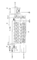
- FIG. 2 is a circuit diagram showing a configuration of a time detection circuit according to the first embodiment of the present invention.
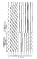
- 3 is a timing chart showing the operation of the time detection circuit according to the first embodiment of the present invention.
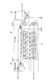
- FIG. 5 is a circuit diagram showing a configuration of a time detection circuit according to a second embodiment of the present invention.
- 6 is a timing chart showing the operation of the time detection circuit according to the second embodiment of the present invention.
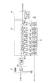
- FIG. 6 is a circuit diagram showing a configuration of a time detection circuit according to a third embodiment of the present invention. 6 is a timing chart showing the operation of the time detection circuit according to the third embodiment of the present invention.
- FIG. 6 is a block diagram showing a configuration of a solid-state imaging device according to a fourth embodiment of the present invention. It is a circuit diagram which shows the structure of the conventional time detection circuit. It is a timing chart which shows operation
- FIG. 1 shows an example of the configuration of the time detection circuit according to the present embodiment.
- the time detection circuit shown in FIG. 1 includes a delay unit 30, a signal generation unit 32, a latch unit 33, and a count unit.
- the delay unit 30 includes a plurality of delay units DU [0] to DU [7] that output an input signal with a delay.
- the signal generator 32 generates a control signal for controlling the operation of the latch unit 33 and the count unit 34.
- the control signal for causing the latch circuits D_0 to D_6 and the count unit 34 to execute the latch is generated at a third timing after a predetermined time has elapsed from the second timing.
- the latch unit 33 includes latch circuits D_0 to D_7 that latch the logic states of the outputs CK0 to CK7 of the delay unit 30.
- the latch unit 33 includes an AND circuit that outputs a signal Hold_C obtained by ANDing the output xLO_D of the inverting delay circuit DLY of the signal generation unit 32 and the control signal Enable to the latch circuit DU [7].
- the count unit 34 has a counter circuit that performs counting based on the output CK7 from the delay unit 30.
- the latch circuits D_0 to D_6 constituting the latch unit 33 are enabled (valid) when the output Hold_L of the AND circuit of the signal generation unit 32 is High, and the output CK0 of the delay units DU [0] to DU [6] Outputs CK6 as it is.
- the latch circuits D_0 to D_6 are disabled (invalid) when the output Hold_L of the AND circuit of the signal generation unit 32 transits from High to Low, and the delay units DU [0] to DU [6] at that time The logic state corresponding to the outputs CK0 to CK6 is latched.
- the latch circuit D_7 constituting the latch unit 33 is enabled (valid) when the output Hold_C of the AND circuit of the latch unit 33 is High, and outputs the output CK7 of the delay unit DU [7] as it is. Also, the latch circuit D_7 is disabled (invalid) when the output Hold_C of the AND circuit of the latch unit 33 transits from High to Low, and the logic state corresponding to the output CK7 of the delay unit DU [7] at that time Latch.
- the control signal Enable is a signal for controlling the AND circuit of the latch unit 33.
- the control signal RST is a signal for performing a reset operation of the counter circuit constituting the count unit 34.
- the count latch circuit that latches the logical state of the count result of the count unit 34 is not clearly shown, but the counter circuit also serves as the count latch circuit by using a counter circuit having a latch function.
- this structure is an example to the last, and is not restricted to this.
- FIG. 2 shows the operation of the time detection circuit according to the present embodiment.
- a clock having a period substantially matching the delay time of the delay unit 30 is input (first timing).
- the delay units DU [1] to DU [7] constituting the delay unit 30 are The outputs of the preceding delay units are inverted and delayed, and output as outputs CK1 to CK7.
- the latch circuit D_7 since the output Hold_C of the AND circuit of the latch unit 33 is High, the latch circuit D_7 is in an enabled state and outputs the output CK7 of the delay unit DU [7] as it is.
- the count unit 34 performs a count operation based on the output CK7 of the delay unit 30 output as the output Q7 of the latch circuit D_7. In this count operation, the count value increases or decreases at the rise or fall of the output CK7.
- the latch circuits D_0 to D_6 are enabled.
- the output xLO_D of the inverting delay circuit DLY of the signal generating unit 32 is inverted, and the signal The output Hold_L of the AND circuit of the generation unit 32 becomes Low.
- the latch circuits D_0 to D_6 are disabled.
- logic states corresponding to the outputs CK0 to CK6 of the delay units DU [0] to DU [6] are latched in the latch circuits D_0 to D_6 of the latch unit 33.
- the latch circuit D_7 is disabled, and the logic state corresponding to the output CK7 of the delay unit DU [7] is changed to the latch unit 33. Is latched by the latch circuit D_7.
- the count unit 34 latches the count value when the latch circuit D_7 stops its operation. Data corresponding to “detected time” is obtained from the logic state latched by the latch unit 33 and the count value latched by the count unit 34.
- the latched data is output to, for example, a subsequent arithmetic unit (not shown), and processing such as binarization is performed.
- the power consumption is reduced by controlling the operations of the latch circuits D_0 to D_6 constituting the latch unit 33.
- a configuration for controlling the latch circuits D_1 to D_5 may be used. .
- FIG. 3 shows an example of the configuration of the time detection circuit according to the present embodiment.
- the configuration diagram of this example will be described below.
- the configuration of the delay unit 30 is different from the configuration shown in FIG.
- an annular delay circuit is realized by connecting a plurality of delay units DU [*] (* is 0 to 7) constituting the delay unit 30 in a ring shape. Other than this, it is the same as FIG.
- FIG. 4 shows the operation of the time detection circuit according to this embodiment.
- the rest is the same as in FIG.
- FIG. 5 shows an example of the configuration of the time detection circuit according to the present embodiment.
- the configuration diagram of this example will be described below.
- the illustration of the delay unit 30 is omitted.
- the difference from the configuration shown in FIG. 3 is that a comparison unit 31 is added.
- the comparison unit 31 receives an analog signal Signal to be time-detected and a ramp wave Ramp that increases or decreases over time, and outputs a signal indicating a result of comparing the analog signal Signal and the ramp wave Ramp. Consists of a comparator. As a result, a time interval (corresponding to “detected time” in the description of FIG. 2) corresponding to the analog signal Signal is generated. The rest is the same as in FIG.
- the delay unit 30 starts operating.
- the delay units DU [1] to DU [7] constituting the delay unit 30 are The outputs of the preceding delay units are inverted and delayed, and output as outputs CK1 to CK7.
- Outputs CK0 to CK7 of the delay units DU [0] to DU [7] are input to the latch circuits D_0 to D_7 of the latch unit 33. Since the input CO of the inverting delay circuit DLY is Low and the output Hold_L of the AND circuit of the signal generation unit 32 is Low, the latch circuits D_0 to D_6 are in a disabled state and stop operating.
- the latch circuit D_7 since the output Hold_C of the AND circuit of the latch unit 33 is High, the latch circuit D_7 is in an enabled state and outputs the output CK7 of the delay unit DU [7] as it is.
- the count unit 34 performs a count operation based on the output CK7 of the delay unit 30 output as the output Q7 of the latch circuit D_7. In this count operation, the count value increases or decreases at the rise or fall of the output CK7.
- the output CO of the comparison unit 31 is inverted and becomes High at the timing (second timing) at which the analog signal Signal and the ramp wave Ramp substantially coincide.
- the latch circuits D_0 to D_6 are enabled.
- the output xCO_D of the inverting delay circuit DLY of the signal generating unit 32 is inverted, and the signal The output Hold_L of the AND circuit of the generation unit 32 becomes Low.
- the latch circuits D_0 to D_6 are disabled.
- logic states corresponding to the outputs CK0 to CK6 of the delay units DU [0] to DU [6] are latched in the latch circuits D_0 to D_6 of the latch unit 33.
- the latch circuit D_7 since the output Hold_C of the AND circuit of the latch unit 33 becomes Low at the third timing, the latch circuit D_7 is disabled, and the logic state corresponding to the output CK7 of the delay unit DU [7] is changed to the latch unit 33. Is latched by the latch circuit D_7.
- the count unit 34 latches the count value when the latch circuit D_7 stops its operation. Data corresponding to the time interval from the first timing to the second timing is obtained by the logic state latched by the latch unit 33 and the count value latched by the count unit 34.
- the latched data is output to, for example, a subsequent arithmetic unit (not shown), and processing such as binarization is performed.
- the power consumption is reduced by controlling the operations of the latch circuits D_0 to D_6 constituting the latch unit 33.
- a configuration for controlling the latch circuits D_1 to D_5 may be used. .
- FIG. 7 shows an example of the configuration of the solid-state imaging device according to the present embodiment.
- the configuration diagram of this example will be described below.
- 7 includes an imaging unit 2, a vertical selection unit 12, a read current source unit 5, an analog unit 6, a delay unit 18, a ramp unit 19, a column processing unit 15, a horizontal selection unit 14, and a calculation unit 17.
- the control unit 20 is configured.
- the imaging unit 2 includes a plurality of unit pixels 3 that generate and output a signal corresponding to the magnitude of an incident electromagnetic wave in a matrix.
- the vertical selection unit 12 selects each row of the imaging unit 2.
- the read current source unit 5 reads the signal from the imaging unit 2 as a voltage signal.
- the analog unit 6 performs analog processing on the signal read from the imaging unit 2.
- the delay unit 18 corresponds to the delay unit 30 described in the second and third embodiments, and includes an annular delay circuit 8.
- the ramp unit 19 generates a ramp wave as a reference signal that increases or decreases over time.
- the column processing unit 15 is connected to the lamp unit 19 via a reference signal line 119.
- the horizontal selection unit 14 reads the data generated by the column processing unit 15 to the horizontal signal line 117.
- the arithmetic unit 17 is connected to the horizontal signal line 117.
- the control unit 20 controls each unit.
- each row or each column of the imaging unit 2 has several tens of Tens of thousands of unit pixels 3 are arranged.
- the unit pixel 3 constituting the imaging unit 2 is configured by a photoelectric conversion element such as a photodiode / photogate / phototransistor and a transistor circuit.
- peripheral drive systems and signal processing systems that drive and control each unit pixel 3 of the imaging unit 2, that is, a vertical selection unit 12, a horizontal selection unit 14, a column processing unit 15, a calculation unit 17, a delay unit 18, Peripheral circuits such as the lamp unit 19 and the control unit 20 are integrally formed with the imaging unit 2 in a semiconductor region such as single crystal silicon using a technique similar to the semiconductor integrated circuit manufacturing technique.
- unit pixels 3 are arranged two-dimensionally by 4 rows and 6 columns, and row control lines 11 are wired for each row with respect to the pixel array of 4 rows and 6 columns.
- Each one end of the row control line 11 is connected to each output end corresponding to each row of the vertical selection unit 12.
- the vertical selection unit 12 includes a shift register or a decoder, and controls the row address and row scanning of the imaging unit 2 via the row control line 11 when driving each unit pixel 3 of the imaging unit 2.
- a vertical signal line 13 is wired for each column with respect to the pixel array of the imaging unit 2.
- the read current source unit 5 is configured using, for example, an NMOS transistor.
- a vertical signal line 13 from the imaging unit 2 is connected to the drain terminal, a desired voltage is appropriately applied to the control terminal, and a source terminal is connected to GND. As a result, a signal from the unit pixel 3 is output as a voltage mode.
- an NMOS transistor is used as the current source has been described, the present invention is not limited to this.
- the analog unit 6 is the difference between the signal level immediately after the pixel reset (reset level) and the true signal level with respect to the voltage mode pixel signal input via the vertical signal line 13.
- AGC Auto Gain Control circuit having a signal amplification function may be provided.
- the column processing unit 15 includes, for example, an ADC unit 16 provided for each pixel column of the imaging unit 2, that is, for each vertical signal line 13, and passes through the vertical signal line 13 from each unit pixel 3 of the imaging unit 2 for each pixel column.
- the read analog pixel signal is converted into digital data.
- the ADC unit 16 is arranged with a one-to-one correspondence with the pixel column of the imaging unit 2, but this is only an example and is limited to this arrangement relationship. is not.
- one ADC unit 16 may be arranged for a plurality of pixel columns, and the one ADC unit 16 may be used in a time-sharing manner between the plurality of pixel columns.
- VCO Voltage Controlled Oscillator
- a so-called asymmetric oscillation circuit whose output is equivalently even (especially a power of 2) may be used.
- the circuit or ring delay circuit itself is composed of an even number (especially a power of 2) delay units, and the output of the final stage of the fully differential inverting circuit constituting the delay unit is the inverse of the input of the first stage.
- a so-called fully differential oscillation circuit configured by being fed back to the side may be used.
- An annular delay circuit is suitable as the delay unit 18, but it is not necessary to be limited thereto.
- the ramp unit 19 is constituted by, for example, an integration circuit, generates a so-called ramp wave whose level changes in an inclined manner as time elapses according to the control by the control unit 20, and the voltage comparison unit 131 via the reference signal line 119. To one of the input terminals.
- the ramp unit 19 is not limited to the one using an integration circuit, and a DAC circuit may be used. However, in the case of adopting a configuration in which a ramp wave is generated digitally using a DAC circuit, it is necessary to make the step of the ramp wave fine or a configuration equivalent thereto.
- the horizontal selection unit 14 includes a shift register or a decoder, and controls the column address and column scanning of the ADC unit 16 of the column processing unit 15. Under the control of the horizontal selection unit 14, the digital data AD-converted by the ADC unit 16 is sequentially read out to the horizontal signal line 117.
- the calculation unit 17 performs code conversion such as binarization based on the digital data output to the horizontal signal line 117, and outputs binarized digital data. Further, the calculation unit 17 may incorporate signal processing functions such as black level adjustment, column variation correction, and color processing. Furthermore, n-bit parallel digital data may be converted into serial data and output.
- the control unit 20 may be provided as a separate semiconductor integrated circuit independent of other functional elements such as the imaging unit 2, the vertical selection unit 12, and the horizontal selection unit 14.
- an imaging device which is an example of a semiconductor system is constructed by the imaging device including the imaging unit 2, the vertical selection unit 12, the horizontal selection unit 14, and the like and the control unit 20.
- This imaging apparatus may be provided as an imaging module in which peripheral signal processing, a power supply circuit, and the like are also incorporated.
- Each of the ADC units 16 compares the analog pixel signal read from each unit pixel 3 of the imaging unit 2 through the vertical signal line 13 with a ramp wave supplied from the ramp unit 19 for AD conversion, thereby obtaining a pixel signal.
- a time interval having a size (pulse width) in the time axis direction corresponding to the size of is generated.
- AD conversion is performed by using data corresponding to the time interval as digital data corresponding to the magnitude of the pixel signal.
- the ADC unit 16 is provided for each column. In FIG. 7, six ADC units 16 are provided. The ADC units 16 in each column have the same configuration.
- the ADC unit 16 includes a voltage comparison unit 131, a latch control unit 132, a latch unit 133, and a column counter 134.
- the voltage comparison unit 131 which is an example of a comparison unit, generates a signal voltage corresponding to an analog pixel signal output from the unit pixel 3 of the imaging unit 2 through the vertical signal line 13, and a ramp wave supplied from the ramp unit 19. By comparing, the magnitude of the pixel signal is converted into a time interval (pulse width) which is information in the time axis direction.
- the comparison output of the voltage comparison unit 131 becomes, for example, a low level when the lamp voltage is larger than the signal voltage, and becomes a high level when the lamp voltage is less than or equal to the signal voltage.
- the latch control unit 132 Based on the comparison output of the voltage comparison unit 131, the latch control unit 132 generates a control signal for controlling the latch unit 133 and the column counter 134.
- the latch unit 133 includes latch circuits D_0 to D_6 and a latch circuit D_7.
- the latch circuits D_0 to D_6 constituting the latch unit 133 are enabled at a timing (second timing) when the comparison output of the voltage comparison unit 131 is received and the comparison output is inverted. After a predetermined time has elapsed from the second timing (third timing), each of the latch circuits D_0 to D_7 of the latch unit 133 is disabled, so that the logic state generated by the delay unit 18 is latched ( Hold / remember).
- the column counter 134 performs counting based on the output of the latch circuit D_7 of the latch unit 133.
- the column counter 134 is assumed to be a counter circuit having a latch function for holding the logical state of the column counter 134.
- the lower data signal indicated by the logic state of the latch unit 133 is, for example, 8-bit data.
- the upper data signal indicated by the count result of the column counter 134 is, for example, 10-bit data.
- the 10 bits are merely an example, and the number of bits may be less than 10 bits (for example, 8 bits) or the number of bits may be more than 10 bits (for example, 12 bits).
- the unit pixel 3 outputs a reset level and a signal level.
- the output reset level and signal level are output as a pixel output signal subjected to CDS processing in the analog unit 6.
- AD conversion is performed as follows. For example, a ramp wave that falls with a predetermined inclination is compared with a pixel output signal, and a point in time when the pixel output signal and the ramp voltage of the ramp wave coincide with each other from the time point (first timing) related to the start of this comparison process (The period from the second timing) to the end of the predetermined time (third timing) is the output from the annular delay circuit (for example, CK7, that is, the output of the latch circuit D_7 of the latch unit 33 shown in FIG. 5) And a logical state of a multi-phase clock (CK0 to CK7, that is, corresponding to the output Q of the latch circuit D_0 to D_7 of the latch unit 33 shown in FIG.
- the control unit 20 supplies the ramp unit 19 with control data for ramp wave generation.
- the ramp unit 19 outputs a ramp wave that changes in a ramp shape over time as a comparison voltage applied to one input terminal of the voltage comparison unit 131 as a whole.
- the voltage comparison unit 131 starts comparison between the ramp wave and the pixel output signal (first timing). Further, the control unit 20 changes the start pulse output to the annular delay circuit 8 from Low to High at the first timing.
- the voltage comparison unit 131 compares the ramp wave supplied from the ramp unit 19 with the pixel output signal, and outputs a comparison output when both voltages substantially coincide (second timing). The comparison output is further inverted or delayed (third timing). At the second timing, the latch circuits D_0 to D_6 of the latch unit 133 are enabled based on the comparison output of the voltage comparator 131, and at the third timing, the latch circuits D_0 to D_7 of the latch unit 133 are disabled. The logic state corresponding to the output from the delay unit 18 is latched. The column counter 134 latches the count value when the latch circuit D_7 of the latch unit 133 is stopped. Thereby, digital data (data signal) corresponding to the pixel output signal is obtained. The control unit 20 stops the supply of control data to the ramp unit 19 and the output from the delay unit 18 when a predetermined period has elapsed. As a result, the ramp unit 19 stops generating the ramp wave.
- the digital data is output by the horizontal selection unit 14 via the horizontal signal line 117 and transferred to the calculation unit 17.
- the arithmetic unit 17 binary data is obtained by performing binarization processing. Note that the calculation unit 17 may be built in the column processing unit 15.
- the power consumption is reduced by controlling the operations of the latch circuits D_0 to D_6 constituting the latch unit 133.
- a configuration for controlling the latch circuits D_1 to D_5 may be used. .
- the present invention it is possible to provide a time detection circuit, an AD converter, and a solid-state imaging device with reduced current consumption by shortening the operation time of the latch unit.
Landscapes
- Engineering & Computer Science (AREA)
- Multimedia (AREA)
- Signal Processing (AREA)
- Theoretical Computer Science (AREA)
- Physics & Mathematics (AREA)
- General Physics & Mathematics (AREA)
- Transforming Light Signals Into Electric Signals (AREA)
- Analogue/Digital Conversion (AREA)
Abstract
本発明は、入力信号(Start P)を遅延させて出力する複数の遅延ユニット(DU)を有し、第1のパルスの入力に係る第1のタイミングで動作を開始する遅延部(30)と、前記複数の遅延ユニット(DU)の論理状態をラッチするラッチ部(33)と、前記複数の遅延ユニットのいずれか(DU[7])から出力されるクロック(CK7)に基づいてカウントを行うカウント部(34)と、第2のパルスの入力に係る第2のタイミングで前記ラッチ部(33)を有効にし、前記第2のタイミングから所定の時間だけ経過した第3のタイミングで前記ラッチ部(33)にラッチを実行させるラッチ制御部(32)と、を有する時間検出回路である。ラッチ部(33)を構成するラッチ回路(D_0-D_6)が、第2のパルスの入力があるまで(被検出時間の間)ディスエーブル状態(保持状態)を維持するため、ラッチ部(33)の消費電流を低減することができる。
Description
本発明は、時間検出回路およびそれを用いたAD変換器、固体撮像装置に関する。
本願は、2010年8月6日に、日本に出願された特願2010-177756号に基づき優先権を主張し、その内容をここに援用する。
本願は、2010年8月6日に、日本に出願された特願2010-177756号に基づき優先権を主張し、その内容をここに援用する。
従来の時間検出回路の一例として、図8に示した構成(例えば、特許文献1,2参照)が知られている。初めに、図8の時間検出回路の構成および動作について説明する。
図8は、従来例に係る時間検出回路の構成を示している。図8に示す時間検出回路は、遅延部30、比較部31、ラッチ部33、およびカウント部34で構成される。遅延部30は、入力信号を遅延させて出力する複数の遅延ユニットDU[0]~DU[7]を有する。先頭の遅延ユニットDU[0]にスタートパルス(=StartP)が入力される。比較部31は、時間検出の対象となるアナログ信号Signalと、時間の経過と共に減少するランプ波Rampとが入力され、アナログ信号Signalとランプ波Rampを比較した結果を示す信号を出力する電圧比較器を有する。ラッチ部33は、遅延部30の出力CK0~CK7の論理状態をラッチするラッチ回路D_0~D_7を有する。カウント部34は、遅延部30からの出力CK7に基づいてカウントを行うカウンタ回路を有する。
比較部31において、アナログ信号Signalの振幅に応じたタイムインターバル(時間軸方向の大きさ)が生成される。バッファ回路は、入力信号を反転して出力する反転バッファ回路である。ここでは、本明細書中の説明を理解し易くするために反転バッファ回路の構成としている。
ラッチ部33を構成するラッチ回路D_0~D_7は、バッファ回路の出力HoldがHighのときにイネーブル(有効)状態であり、遅延ユニットDU[0]~DU[7]の出力CK0~CK7をそのまま出力する。また、ラッチ回路D_0~D_7は、バッファ回路の出力HoldがHighからLowに遷移するときにディスエーブル(無効)状態となり、そのときの遅延ユニットDU[0]~DU[7]の出力CK0~CK7に応じた論理状態をラッチする。
制御信号RSTは、カウント部34を構成するカウンタ回路のリセット動作を行うための信号である。尚、カウント部34のカウント結果の論理状態をラッチするカウントラッチ回路を明示していないが、ラッチ機能を有するカウンタ回路を用いることにより、カウンタ回路がカウントラッチ回路を兼ねている。
次に、従来例の動作について説明する。図9は、従来例に係る時間検出回路の動作を示している。
まず、比較部31での比較開始に係るタイミング(第1のタイミング)で、スタートパルス(=StartP)として、遅延部30の遅延時間に略一致する周期のクロックが遅延部30に入力される。これにより、遅延部30が動作を開始する。遅延部30を構成する遅延ユニットDU[0]は、スタートパルス(=StartP)を反転および遅延させて出力CK0として出力し、遅延部30を構成する遅延ユニットDU[1」~DU[7]はそれぞれ前段の遅延ユニットの出力を反転および遅延させて出力CK1~CK7として出力する。遅延ユニットDU[0]~DU[7]の出力CK0~CK7はラッチ部33のラッチ回路D_0~D_7に入力される。バッファ回路の出力HoldがHighであるため、ラッチ回路D_0~D_7はイネーブル状態であり、遅延ユニットDU[0]~DU[7]の出力CK0~CK7をそのまま出力する。
カウント部34は、ラッチ部33のラッチ回路D_7の出力Q7として出力される遅延部30の出力CK7に基づいてカウント動作を行う。このカウント動作では、出力CK7の立上りまたは立下りでカウント値が増加または減少する。アナログ信号Signalとランプ波Rampとが略一致したタイミング(第2のタイミング)で出力COが反転する。比較部31の出力COがバッファ回路でバッファリングされた後(第3のタイミング)、バッファ回路の出力HoldがLowとなる。
これにより、ラッチ回路D_0~D_7がディスエーブル状態となる。このとき、遅延ユニットDU[0]~DU[7]の出力CK0~CK7に応じた論理状態がラッチ回路D_0~D_7にラッチされる。
カウント部34は、ラッチ回路D_7が動作を停止することでカウント値をラッチする。ラッチ部33がラッチしている論理状態と、カウント部34がラッチしているカウント値とにより、アナログ信号Signalに対応したデータが得られる。
カウント部34は、ラッチ回路D_7が動作を停止することでカウント値をラッチする。ラッチ部33がラッチしている論理状態と、カウント部34がラッチしているカウント値とにより、アナログ信号Signalに対応したデータが得られる。
上記従来例に係る時間検出回路によれば、タイムインターバルに対応したデータを得ることができる。すなわち、タイムインターバルに対応した時間を検出することができる。
上記の時間検出回路を利用して、アナログ信号をデジタル信号に変換するAD変換器を構成することもできる。
上記の時間検出回路を利用して、アナログ信号をデジタル信号に変換するAD変換器を構成することもできる。
上記従来の時間検出回路では、ラッチ部33を構成するラッチ回路D_0~D_6がタイムインターバルの期間動作することにより、ラッチ部33で消費される電流値が大きくなり、時間検出回路の低消費電流化が困難である。
従来例の時間検出回路では、第1のタイミングから第3のタイミングまでの期間、ラッチ部33を構成するラッチ回路D_0~D_6が常に動作している。遅延部30の出力CK0~CK7は、一般的に周波数が高いため、ラッチ部33を構成するラッチ回路D_0~D_6で消費される電流により、時間検出回路自体の低消費電流化が困難となっている。
ここで、従来例の時間検出回路をAD変換器に用いた具体的デバイスの例として、デジタルスチルカメラ(DSC)等に使用されるイメージャを考えてみる。具体的には、画素数は2000万画素、フレームレートは60frame/secというスペックを仮定してみる。尚、AD変換器は画素列ごとに配置するものとする。説明を容易にするため、2000万画素の画素配列を縦横に4000行×5000列とし、更に単純化のためにブランキング期間がないものとすると、1秒当りに画素信号を読み出す行の数は、以下のようになる。
60frame/sec×4000行/frame=240Kline/sec
60frame/sec×4000行/frame=240Kline/sec
つまり、1行の読出しレートは240KHzとなる。例えば10ビットのAD変換を、上位7ビット(カウント部34のカウント値)と下位3ビット(ラッチ部33を構成するラッチ回路D_0~D_7のデータ)で構成したとすると、1行の読出しレートの128(=27)倍、すなわち30MHz程度で遅延部30からクロックCK0~CK7が出力される必要がある。ここで、ラッチ部33を構成するラッチ回路1個当りの消費電流値を1uA/個と仮定すると、1列当りのラッチ回路D_0~D_6での消費電流値は、
1uA/個×7個=7uA
となる。尚、ラッチ回路D_7の出力は、カウント部34を構成するカウンタ回路のカウントクロックとして用いるため計算には含めていない。
1uA/個×7個=7uA
となる。尚、ラッチ回路D_7の出力は、カウント部34を構成するカウンタ回路のカウントクロックとして用いるため計算には含めていない。
つまり、5000列での消費電流値は35mAとなる。この計算では、AD変換器が画素からデータを受け取るまでの待機期間等の、AD変換としての比較動作ができない期間を考慮しておらず、また、上記画素以外にOB(Optical Black)画素から画素信号を読み出す期間やブランキング期間を除いているため、実際には、上記のように見積もった周波数30MHzよりも高い周波数になると考えられる。
本発明は、消費電流を低減することができる時間検出回路、AD変換器、および固体撮像装置を提供する。
本発明の時間検出回路は、入力信号を遅延させて出力する複数の遅延ユニットを有し、第1のパルスの入力に係る第1のタイミングで動作を開始する遅延部と、前記複数の遅延ユニットの論理状態をラッチするラッチ部と、前記複数の遅延ユニットのいずれかから出力されるクロックに基づいてカウントを行うカウント部と、前記カウント部の状態をラッチするカウントラッチ部と、第2のパルスの入力に係る第2のタイミングで前記ラッチ部を有効にし、前記第2のタイミングから所定の時間だけ経過した第3のタイミングで前記ラッチ部および前記カウントラッチ部にラッチを実行させるラッチ制御部と、を有する。
好ましくは、前記遅延部は、前記複数の遅延ユニットが円環状に接続された円環遅延回路であってもよい。
好ましくは、所定のアナログ信号と、時間の経過とともに増加または減少する参照信号とが入力され、前記参照信号が前記アナログ信号に対して所定の条件をみたしたときに比較信号を出力する比較部を更に有し、前記ラッチ制御部に前記比較信号が入力され、前記第1のタイミングは、前記参照信号が前記比較部に入力されるタイミングに係り、前記第2のタイミングは、前記比較信号が前記ラッチ制御部に入力されるタイミングに係ってもよい。
また、本発明のAD変換器は、上記の時間検出回路と、前記参照信号を生成する参照信号生成部と、前記ラッチ部にラッチされた前記論理状態と、前記カウントラッチ部がラッチした前記状態とに基づいてデジタル信号を生成する演算部と、を有する。
また、本発明の固体撮像装置は、入射される電磁波の大きさに応じて画素信号を出力する画素が複数、行列状に配置された撮像部と、前記画素信号に応じた前記アナログ信号が入力される上記のAD変換器と、を有し、前記比較部、前記ラッチ部、前記カウント部、前記カウントラッチ部、および前記ラッチ制御部は、前記撮像部を構成する前記画素の1列または複数列ごとに設けられる。
本発明によれば、第2のパルスの入力に係る第2のタイミングでラッチ部を有効にし、第2のタイミングから所定の時間だけ経過した第3のタイミングでラッチ部およびカウントラッチ部にラッチを実行させることによって、ラッチ部の動作時間が短縮されるので、消費電流を低減することができる。
以下、図面を参照し、本発明の実施形態を説明する。
(第1の実施形態)
まず、本発明の第1の実施形態を説明する。図1は、本実施形態に係る時間検出回路の構成の一例を示している。以下、本例の構成について説明する。図1に示す時間検出回路は、遅延部30、信号生成部32、ラッチ部33、およびカウント部34で構成される。
まず、本発明の第1の実施形態を説明する。図1は、本実施形態に係る時間検出回路の構成の一例を示している。以下、本例の構成について説明する。図1に示す時間検出回路は、遅延部30、信号生成部32、ラッチ部33、およびカウント部34で構成される。
遅延部30は、入力信号を遅延させて出力する複数の遅延ユニットDU[0]~DU[7]を有する。先頭の遅延ユニットDU[0]にスタートパルス(=StartP)が入力される。
信号生成部32は、ラッチ部33およびカウント部34の動作を制御する制御信号を生成する。信号生成部32は、時間検出の対象となるアナログ信号Signalを反転および遅延させる反転遅延回路DLYと、反転遅延回路DLYの入力LO(=Signal)と反転遅延回路DLYの出力xLO_Dとの論理積(AND)をとった信号を出力するAND回路とを有する。詳細は後述するが、この構成により、信号生成部32は、第1のタイミングでスタートパルス(=StartP)が入力された後の第2のタイミングでラッチ部33のラッチ回路D_0~D_6をイネーブル(有効)状態にし、第2のタイミングから所定の時間だけ経過した第3のタイミングでラッチ回路D_0~D_6およびカウント部34にラッチを実行させるための制御信号を生成する。
ラッチ部33は、遅延部30の出力CK0~CK7の論理状態をラッチするラッチ回路D_0~D_7を有する。また、ラッチ部33は、信号生成部32の反転遅延回路DLYの出力xLO_Dと制御信号Enableとの論理積(AND)をとった信号Hold_Cをラッチ回路DU[7]へ出力するAND回路を有する。カウント部34は、遅延部30からの出力CK7に基づいてカウントを行うカウンタ回路を有する。
ラッチ部33を構成するラッチ回路D_0~D_6は、信号生成部32のAND回路の出力Hold_LがHighのときにイネーブル(有効)状態であり、遅延ユニットDU[0]~DU[6]の出力CK0~CK6をそのまま出力する。また、ラッチ回路D_0~D_6は、信号生成部32のAND回路の出力Hold_LがHighからLowに遷移するときにディスエーブル(無効)状態となり、そのときの遅延ユニットDU[0]~DU[6]の出力CK0~CK6に応じた論理状態をラッチする。
一方、ラッチ部33を構成するラッチ回路D_7は、ラッチ部33のAND回路の出力Hold_CがHighのときにイネーブル(有効)状態であり、遅延ユニットDU[7]の出力CK7をそのまま出力する。また、ラッチ回路D_7は、ラッチ部33のAND回路の出力Hold_CがHighからLowに遷移するときにディスエーブル(無効)状態となり、そのときの遅延ユニットDU[7]の出力CK7に応じた論理状態をラッチする。
制御信号Enableは、ラッチ部33のAND回路を制御するための信号である。制御信号RSTは、カウント部34を構成するカウンタ回路のリセット動作を行うための信号である。本図では、カウント部34のカウント結果の論理状態をラッチするカウントラッチ回路を明示していないが、ラッチ機能を有するカウンタ回路を用いることにより、カウンタ回路がカウントラッチ回路を兼ねている。尚、本構成はあくまで一例であり、これに限らない。
次に、本例の動作について説明する。図2は、本実施形態に係る時間検出回路の動作を示している。
まず、スタートパルス(=StartP)として、遅延部30の遅延時間に略一致する周期のクロックが入力される(第1のタイミング)。これにより、遅延部30が動作を開始する。遅延部30を構成する遅延ユニットDU[0]は、スタートパルス(=StartP)を反転および遅延させて出力CK0として出力し、遅延部30を構成する遅延ユニットDU[1」~DU[7]はそれぞれ前段の遅延ユニットの出力を反転および遅延させて出力CK1~CK7として出力する。遅延ユニットDU[0]~DU[7]の出力CK0~CK7はラッチ部33のラッチ回路D_0~D_7に入力される。反転遅延回路DLYの入力LO(=Signal)がLowであり、信号生成部32のAND回路の出力Hold_LがLowであるため、ラッチ回路D_0~D_6はディスエーブル状態であり、動作を停止している。
一方、ラッチ部33のAND回路の出力Hold_CがHighであるため、ラッチ回路D_7はイネーブル状態であり、遅延ユニットDU [7]の出力CK7をそのまま出力する。カウント部34は、ラッチ回路D_7の出力Q7として出力される遅延部30の出力CK7に基づいてカウント動作を行う。このカウント動作では、出力CK7の立上りまたは立下りでカウント値が増加または減少する。
第1のタイミングから、検出の対象となる『被検出時間』が経過した後、信号生成部32の反転遅延回路DLYの入力LO(=Signal)が反転することにより、信号生成部32のAND回路の出力Hold_LがHighとなる。これにより、ラッチ回路D_0~D_6はイネーブル状態となる。第2のタイミングから、信号生成部32の反転遅延回路DLYの遅延時間に一致する時間が経過した後(第3のタイミング)、信号生成部32の反転遅延回路DLYの出力xLO_Dが反転し、信号生成部32のAND回路の出力Hold_LがLowとなる。これにより、ラッチ回路D_0~D_6がディスエーブル状態となる。このとき、遅延ユニットDU[0]~DU[6]の出力CK0~CK6に応じた論理状態がラッチ部33のラッチ回路D_0~D_6にラッチされる。
また、上記第3のタイミングでラッチ部33のAND回路の出力Hold_CがLowとなるため、ラッチ回路D_7がディスエーブル状態となり、遅延ユニットDU[7]の出力CK7に応じた論理状態がラッチ部33のラッチ回路D_7にラッチされる。カウント部34は、ラッチ回路D_7が動作を停止することでカウント値をラッチする。ラッチ部33がラッチしている論理状態と、カウント部34がラッチしているカウント値とにより、『被検出時間』に対応したデータが得られる。ラッチされたデータは、例えば後段の演算部(図示せず)に出力され、2進化等の処理が行われる。
上記の動作では、第2のタイミングから第3のタイミングまでの期間のみ、ラッチ回路D_0~D_6が動作するため、ラッチ部33での消費電流を低減することができる。したがって、時間検出回路の消費電流を低減することができる。
尚、本例ではラッチ部33を構成するラッチ回路D_0~D_6の動作を制御することで低消費電力化を実現した構成としているが、例えばラッチ回路D_1~D_5を制御するような構成でも構わない。また、これに限る必要もない。
(第2の実施形態)
次に、本発明の第2の実施形態を説明する。図3は、本実施形態に係る時間検出回路の構成の一例を示している。以下、本例の構成図について説明する。図1に示した構成と異なるのは、遅延部30の構成である。本実施形態では、遅延部30を構成する複数の遅延ユニットDU[*](*は、0~7)をリング状に接続することで円環遅延回路を実現している。これ以外は、図1と同様であるので説明は省略する。
次に、本発明の第2の実施形態を説明する。図3は、本実施形態に係る時間検出回路の構成の一例を示している。以下、本例の構成図について説明する。図1に示した構成と異なるのは、遅延部30の構成である。本実施形態では、遅延部30を構成する複数の遅延ユニットDU[*](*は、0~7)をリング状に接続することで円環遅延回路を実現している。これ以外は、図1と同様であるので説明は省略する。
次に、本例の動作について説明する。図4は、本実施形態に係る時間検出回路の動作を示している。図2と異なるのは、スタートパルス(=StartP)であり、スタートパルス(=StartP)の論理状態がLowからHighに変化することで遅延部30が動作を開始し、遅延部30からの出力CK7に基づいてカウント部34のカウント動作が行われる。これ以外は、図2と同様であるので説明は省略する。
第1の実施形態では、スタートパルス(=StartP)を、遅延部30の遅延時間に略一致する周期のクロックとして生成する必要があったが、本実施形態では、スタートパルス(=StartP)の生成が容易となる。このため、遅延部30の制御すなわち時間検出回路の制御が容易となる。
(第3の実施形態)
次に、本発明の第3の実施形態を説明する。図5は、本実施形態に係る時間検出回路の構成の一例を示している。以下、本例の構成図について説明する。図5では遅延部30の図示を省略している。図3に示した構成と異なるのは、比較部31を追加している点である。比較部31は、時間検出の対象となるアナログ信号Signalと、時間の経過と共に増加あるいは減少するランプ波Rampとが入力され、アナログ信号Signalとランプ波Rampを比較した結果を示す信号を出力する電圧比較器で構成される。これにより、アナログ信号Signalに応じたタイムインターバル(図2の説明における『被検出時間』に相当)が生成されることになる。これ以外は、図3と同様であるので説明は省略する。
次に、本発明の第3の実施形態を説明する。図5は、本実施形態に係る時間検出回路の構成の一例を示している。以下、本例の構成図について説明する。図5では遅延部30の図示を省略している。図3に示した構成と異なるのは、比較部31を追加している点である。比較部31は、時間検出の対象となるアナログ信号Signalと、時間の経過と共に増加あるいは減少するランプ波Rampとが入力され、アナログ信号Signalとランプ波Rampを比較した結果を示す信号を出力する電圧比較器で構成される。これにより、アナログ信号Signalに応じたタイムインターバル(図2の説明における『被検出時間』に相当)が生成されることになる。これ以外は、図3と同様であるので説明は省略する。
次に、本例の動作について説明する。まず、比較部31での比較開始に係るタイミング(第1のタイミング)で、スタートパルス(=StartP)の論理状態がLowからHighに変化する。
これにより、遅延部30が動作を開始する。遅延部30を構成する遅延ユニットDU[0]は、スタートパルス(=StartP)を反転および遅延させて出力CK0として出力し、遅延部30を構成する遅延ユニットDU[1」~DU[7]はそれぞれ前段の遅延ユニットの出力を反転および遅延させて出力CK1~CK7として出力する。遅延ユニットDU[0]~DU[7]の出力CK0~CK7はラッチ部33のラッチ回路D_0~D_7に入力される。反転遅延回路DLYの入力COがLowであり、信号生成部32のAND回路の出力Hold_LがLowであるため、ラッチ回路D_0~D_6はディスエーブル状態であり、動作を停止している。
これにより、遅延部30が動作を開始する。遅延部30を構成する遅延ユニットDU[0]は、スタートパルス(=StartP)を反転および遅延させて出力CK0として出力し、遅延部30を構成する遅延ユニットDU[1」~DU[7]はそれぞれ前段の遅延ユニットの出力を反転および遅延させて出力CK1~CK7として出力する。遅延ユニットDU[0]~DU[7]の出力CK0~CK7はラッチ部33のラッチ回路D_0~D_7に入力される。反転遅延回路DLYの入力COがLowであり、信号生成部32のAND回路の出力Hold_LがLowであるため、ラッチ回路D_0~D_6はディスエーブル状態であり、動作を停止している。
一方、ラッチ部33のAND回路の出力Hold_CがHighであるため、ラッチ回路D_7はイネーブル状態であり、遅延ユニットDU [7]の出力CK7をそのまま出力する。カウント部34は、ラッチ回路D_7の出力Q7として出力される遅延部30の出力CK7に基づいてカウント動作を行う。このカウント動作では、出力CK7の立上りまたは立下りでカウント値が増加または減少する。
アナログ信号Signalとランプ波Rampとが略一致したタイミング(第2のタイミング)で比較部31の出力COが反転し、Highとなる。これにより、ラッチ回路D_0~D_6はイネーブル状態となる。第2のタイミングから、信号生成部32の反転遅延回路DLYの遅延時間に一致する時間が経過した後(第3のタイミング)、信号生成部32の反転遅延回路DLYの出力xCO_Dが反転し、信号生成部32のAND回路の出力Hold_LがLowとなる。これにより、ラッチ回路D_0~D_6がディスエーブル状態となる。このとき、遅延ユニットDU[0]~DU[6]の出力CK0~CK6に応じた論理状態がラッチ部33のラッチ回路D_0~D_6にラッチされる。
また、上記第3のタイミングでラッチ部33のAND回路の出力Hold_CがLowとなるため、ラッチ回路D_7がディスエーブル状態となり、遅延ユニットDU[7]の出力CK7に応じた論理状態がラッチ部33のラッチ回路D_7にラッチされる。カウント部34は、ラッチ回路D_7が動作を停止することでカウント値をラッチする。ラッチ部33がラッチしている論理状態と、カウント部34がラッチしているカウント値とにより、第1のタイミングから第2のタイミングまでのタイムインターバルに対応したデータが得られる。ラッチされたデータは、例えば後段の演算部(図示せず)に出力され、2進化等の処理が行われる。
上記の動作では、第2のタイミングから第3のタイミングまでの期間のみ、ラッチ回路D_0~D_6が動作するため、ラッチ部33での消費電流を低減することができる。したがって、時間検出回路の消費電流を低減することができる。
尚、本例ではラッチ部33を構成するラッチ回路D_0~D_6の動作を制御することで低消費電力化を実現した構成としているが、例えばラッチ回路D_1~D_5を制御するような構成でも構わない。また、これに限る必要もない。
(第4の実施形態)
次に、本発明の第4の実施形態を説明する。図7は、本実施形態に係る固体撮像装置の構成の一例を示している。以下、本例の構成図について説明する。図7に示す固体撮像装置1は、撮像部2、垂直選択部12、読出電流源部5、アナログ部6、遅延部18、ランプ部19、カラム処理部15、水平選択部14、演算部17、制御部20で構成されている。
次に、本発明の第4の実施形態を説明する。図7は、本実施形態に係る固体撮像装置の構成の一例を示している。以下、本例の構成図について説明する。図7に示す固体撮像装置1は、撮像部2、垂直選択部12、読出電流源部5、アナログ部6、遅延部18、ランプ部19、カラム処理部15、水平選択部14、演算部17、制御部20で構成されている。
撮像部2は、入射される電磁波の大きさに応じた信号を生成し出力する単位画素3が複数、行列状に配されている。垂直選択部12は、撮像部2の各行を選択する。読出電流源部5は、撮像部2からの信号を電圧信号として読み出す。アナログ部6は、撮像部2から読み出された信号にアナログ的な処理を施す。遅延部18は、第2、第3の実施形態で説明した遅延部30に対応し、円環遅延回路8を有する。ランプ部19は、時間の経過とともに増加または減少する参照信号としてランプ波を生成する。カラム処理部15は、ランプ部19と参照信号線119を介して接続される。水平選択部14は、カラム処理部15で生成されたデータを水平信号線117に読み出す。演算部17は、水平信号線117に接続されている。制御部20は各部を制御する。
図7では、簡単のため4行×6列の単位画素3から構成される撮像部2の場合について説明しているが、現実には、撮像部2の各行や各列には、数十から数万の単位画素3が配置されることになる。尚、図示を割愛するが、撮像部2を構成する単位画素3は、フォトダイオード/フォトゲート/フォトトランジスタなどの光電変換素子、およびトランジスタ回路によって構成されている。
このシステム構成において、撮像部2の各単位画素3を駆動制御する周辺の駆動系や信号処理系、即ち垂直選択部12、水平選択部14、カラム処理部15、演算部17、遅延部18、ランプ部19、および制御部20などの周辺回路は、撮像部2と共に、半導体集積回路製造技術と同様の技術を用いて単結晶シリコンなどの半導体領域に一体的に形成される。
以下では、各部のより詳細な説明を行う。撮像部2は、単位画素3が4行6列分だけ2次元に配置されるとともに、この4行6列の画素配列に対して行ごとに行制御線11が配線されている。行制御線11の各一端は、垂直選択部12の各行に対応した各出力端に接続されている。垂直選択部12は、シフトレジスタあるいはデコーダなどによって構成され、撮像部2の各単位画素3の駆動に際して、行制御線11を介して撮像部2の行アドレスや行走査の制御を行う。また、撮像部2の画素配列に対して列ごとに垂直信号線13が配線されている。
読出電流源部5は、例えばNMOSトランジスタを用いて構成される。ドレイン端子には撮像部2からの垂直信号線13が接続され、制御端子には適宜所望の電圧が印加され、ソース端子はGNDに接続される。これにより、単位画素3からの信号が電圧モードとして出力されることになる。尚、電流源としてNMOSトランジスタを用いた場合で説明しているがこれに限る必要はない。
アナログ部6は、詳細な説明は省略するが、垂直信号線13を介して入力された電圧モードの画素信号に対して、画素リセット直後の信号レベル(リセットレベル)と真の信号レベルとの差分処理を行うことで、画素ごとの固定なバラツキであるFPN(=Fixed Pattern Noise:固定パターンノイズ)やリセットノイズといわれるノイズ成分を取り除く。尚、必要に応じて信号増幅機能を持つAGC(=Auto Gain Control)回路などを設けても構わない。
カラム処理部15は、例えば撮像部2の画素列ごと、即ち垂直信号線13ごとに設けられたADC部16を有し、撮像部2の各単位画素3から画素列ごとに垂直信号線13を通して読み出されるアナログの画素信号をデジタルデータに変換する。尚、本例では、撮像部2の画素列に対して1対1の対応関係をもってADC部16を配置する構成をとっているが、これは一例に過ぎず、この配置関係に限定されるものではない。例えば、複数の画素列に対してADC部16を1つ配置し、この1つのADC部16を複数の画素列間で時分割にて使用する構成をとることも可能である。カラム処理部15は、後述するランプ部19、遅延部18、および演算部17と共に、撮像部2の選択画素行の単位画素3から読み出されるアナログの画素信号をデジタルの画素データに変換するAD変換器を構成している。
遅延部18は、円環遅延回路である対称発振回路であるVCO(=Voltage Controlled Oscillator)回路に限らず、対称発振回路と同様に円環遅延回路自体は奇数個の遅延ユニットで構成されるが、その出力は等価的に偶数(特に、2のべき乗)である所謂非対称発振回路を用いても構わない。更に、円環遅延回路自体が偶数個(特に、2のべき乗個)の遅延ユニットで構成され、下位論理状態の出力(端子)が偶数(特に、2のべき乗)となるRDL(=Ring Delay Line)回路や円環遅延回路自体が偶数個(特に、2のべき乗個)の遅延ユニットで構成され、更に遅延ユニットを構成する全差動型反転回路の最終段の出力がそれぞれ初段の入力の逆側に帰還されて構成される所謂全差動型発振回路を用いても構わない。尚、遅延部18として円環遅延回路が好適であるが、それに限る必要もない。
ランプ部19は、例えば積分回路によって構成され、制御部20による制御に従って、時間が経過するにつれてレベルが傾斜状に変化する、いわゆるランプ波を生成し、参照信号線119を介して電圧比較部131の入力端子の一方に供給する。尚、ランプ部19としては、積分回路を用いたものに限られるものではなく、DAC回路を用いても構わない。ただし、DAC回路を用いてデジタル的にランプ波を生成する構成をとる場合には、ランプ波のステップを細かくする、あるいはそれと同等な構成をとる必要がある。
水平選択部14は、シフトレジスタあるいはデコーダなどによって構成され、カラム処理部15のADC部16の列アドレスや列走査の制御を行う。この水平選択部14による制御に従って、ADC部16でAD変換されたデジタルデータは順に水平信号線117に読み出される。
演算部17は、水平信号線117に出力されたデジタルデータに基づいてバイナリ化等のコード変換を実施し、2進化したデジタルデータを出力する。また、演算部17は、例えば黒レベル調整、列バラツキ補正、色処理などの信号処理機能を内蔵しても構わない。更に、nビットパラレルのデジタルデータをシリアルデータに変換して出力するようにしても構わない。
制御部20は、ランプ部19、遅延部18、垂直選択部12、水平選択部14、演算部17などの各部の動作に必要なクロックや所定タイミングのパルス信号を供給するTG(=Timing Generator:タイミングジェネレータ)の機能ブロックと、このTGと通信を行うための機能ブロックとを備える。尚、制御部20は、撮像部2や垂直選択部12および水平選択部14など、他の機能要素とは独立して、別の半導体集積回路として提供されても構わない。その場合、撮像部2や垂直選択部12および水平選択部14などからなる撮像デバイスと制御部20とにより、半導体システムの一例である撮像装置が構築される。この撮像装置は、周辺の信号処理や電源回路なども組み込まれた撮像モジュールとして提供されても構わない。
次に、ADC部16の構成について説明する。ADC部16は各々、撮像部2の各単位画素3から垂直信号線13を通して読み出されるアナログの画素信号を、ランプ部19から与えられる、AD変換するためのランプ波と比較することにより、画素信号の大きさに対応した時間軸方向の大きさ(パルス幅)を持つタイムインターバルを生成する。そして、このタイムインターバルに対応したデータを画素信号の大きさに応じたデジタルデータとすることによってAD変換を行う。
以下では、ADC部16の構成の詳細について説明する。ADC部16は列ごとに設けられており、図7では6個のADC部16が設けられている。各列のADC部16は同一の構成となっている。ADC部16は、電圧比較部131、ラッチ制御部132、ラッチ部133、カラムカウンタ134で構成される。
比較部の一例である電圧比較部131は、撮像部2の単位画素3から垂直信号線13を通して出力されるアナログの画素信号に応じた信号電圧と、ランプ部19から供給されるランプ波とを比較することによって、画素信号の大きさを、時間軸方向の情報であるタイムインターバル(パルス幅)に変換する。電圧比較部131の比較出力は、例えばランプ電圧が信号電圧よりも大なるときにはLowレベルになり、ランプ電圧が信号電圧以下のときにはHighレベルになる。ラッチ制御部132は、電圧比較部131の比較出力に基づいて、ラッチ部133およびカラムカウンタ134を制御するための制御信号を生成する。
ラッチ部133は、ラッチ回路D_0~D_6およびラッチ回路D_7を有する。電圧比較部131の比較出力を受けて、この比較出力が反転するタイミング(第2のタイミング)で、ラッチ部133を構成するラッチ回路D_0~D_6がイネーブル状態となる。第2のタイミングから所定の時間が経過した後(第3のタイミング)、ラッチ部133の各ラッチ回路D_0~D_7がディスエーブル状態となることで、遅延部18で生成された論理状態をラッチ(保持/記憶)する。カラムカウンタ134は、ラッチ部133のラッチ回路D_7の出力に基づいてカウントを行う。ここで、カラムカウンタ134は、カラムカウンタ134の論理状態を保持するラッチ機能を合わせ持つカウンタ回路を想定している。
ここで、ラッチ部133の論理状態が示す下位データ信号は、例えば8ビットのデータである。また、カラムカウンタ134のカウント結果が示す上位データ信号は、例えば10ビットのデータである。尚、この10ビットは一例であって、10ビット未満のビット数(例えば、8ビット)や10ビットを超えるビット数(例えば、12ビット)などであっても構わない。
次に、本例の動作について説明する。ここでは、単位画素3の具体的な動作については説明を省略するが、周知のように単位画素3ではリセットレベルと信号レベルとが出力される。出力されたリセットレベルと信号レベルは、アナログ部6においてCDS処理された画素出力信号として出力される。
AD変換は、以下のようにして行われる。例えば所定の傾きで下降するランプ波と、画素出力信号とを比較し、この比較処理の開始に係る時点(第1のタイミング)から、画素出力信号とランプ波のランプ電圧とが一致した時点(第2のタイミング)から所定の時間が経過した後(第3のタイミング)までの期間を、円環遅延回路からの出力(例えばCK7、すなわち図5に記載のラッチ部33のラッチ回路D_7の出力Qに相当)に基づくカウントと、一定の位相差を有する多相クロック(CK0~CK7、すなわち図5に記載のラッチ部33のラッチ回路D_0~D_7の出力Qに相当)の論理状態と、を用いて計測することで、画素出力信号に対応したデジタルデータを得る。尚、撮像部2の選択行の各単位画素3から、1回目の読出し動作で画素信号の雑音を含むリセットレベルが読み出してAD変換し、次に、2回目の読出し動作で信号レベル読み出してAD変換し、その後デジタル的にCDS動作することにより、画素出力信号に応じたデジタルデータを得るようにしても構わない。また、これに限る必要もない。
任意の画素行の単位画素3から垂直信号線13へ出力された画素出力信号が安定した後、制御部20は、ランプ部19に対して、ランプ波生成の制御データを供給する。これを受けてランプ部19は、電圧比較部131の一方の入力端子に与える比較電圧として、全体として時間的にランプ状に変化するランプ波を出力する。電圧比較部131は、このランプ波と画素出力信号との比較を開始する(第1のタイミング)。また、制御部20は、この第1のタイミングで、円環遅延回路8へ出力するスタートパルスをLowからHighに変化させる。
電圧比較部131は、ランプ部19から与えられるランプ波と、画素出力信号とを比較し、双方の電圧が略一致したとき(第2のタイミング)に、比較出力を出力する。この比較出力は、更に反転または遅延して出力される(第3のタイミング)。第2のタイミングにおいて、電圧比較部131の比較出力に基づいてラッチ部133のラッチ回路D_0~D_6がイネーブル状態となり、第3のタイミングにおいて、ラッチ部133のラッチ回路D_0~D_7がディスエーブル状態となり、遅延部18からの出力に応じた論理状態をラッチする。カラムカウンタ134は、ラッチ部133のラッチ回路D_7が停止することでカウント値をラッチする。これにより、画素出力信号に応じたデジタルデータ(データ信号)が得られる。制御部20は、所定の期間が経過すると、ランプ部19への制御データの供給と、遅延部18からの出力とを停止する。これにより、ランプ部19は、ランプ波の生成を停止する。
その後、デジタルデータは、水平選択部14により水平信号線117を介して出力され、演算部17に転送される。演算部17において、バイナリ化処理を実施することで2進化データが得られる。尚、演算部17をカラム処理部15に内蔵する構成でも構わない。
上記の動作では、第2のタイミングから第3のタイミングまでの期間のみ、ラッチ回路D_0~D_6が動作するため、ラッチ部33での消費電流を低減することができる。したがって、AD変換器の消費電流、ひいては固体撮像装置の消費電流を低減することができる。
尚、本例ではラッチ部133を構成するラッチ回路D_0~D_6の動作を制御することで低消費電力化を実現した構成としているが、例えばラッチ回路D_1~D_5を制御するような構成でも構わない。また、これに限る必要もない。
以上、図面を参照して本発明の実施形態について詳述してきたが、具体的な構成は上記の実施形態に限られるものではなく、本発明の要旨を逸脱しない範囲の設計変更等も含まれる。
本発明によれば、ラッチ部の動作時間が短縮されることにより、消費電流が低減された時間検出回路、AD変換器、および固体撮像装置を提供することができる。
2 撮像部
5 読出電流源部
6 アナログ部
8 円環遅延回路
12 垂直選択部
14 水平選択部
15 カラム処理部
16 ADC部
17 演算部
18 遅延部
19 ランプ部(参照信号生成部)
20 制御部
30 遅延部
31 比較部
32 信号生成部(ラッチ制御部)
33 ラッチ部
34 カウント部(カウントラッチ部)
131 電圧比較部(比較部)
132 ラッチ制御部
133 ラッチ部
134 カラムカウンタ(カウントラッチ部)
5 読出電流源部
6 アナログ部
8 円環遅延回路
12 垂直選択部
14 水平選択部
15 カラム処理部
16 ADC部
17 演算部
18 遅延部
19 ランプ部(参照信号生成部)
20 制御部
30 遅延部
31 比較部
32 信号生成部(ラッチ制御部)
33 ラッチ部
34 カウント部(カウントラッチ部)
131 電圧比較部(比較部)
132 ラッチ制御部
133 ラッチ部
134 カラムカウンタ(カウントラッチ部)
Claims (8)
- 入力信号を遅延させて出力する複数の遅延ユニットを有し、第1のパルスの入力に係る第1のタイミングで動作を開始する遅延部と、
前記複数の遅延ユニットの論理状態をラッチするラッチ部と、
前記複数の遅延ユニットのいずれかから出力されるクロックに基づいてカウントを行うカウント部と、
前記カウント部の状態をラッチするカウントラッチ部と、
第2のパルスの入力に係る第2のタイミングで前記ラッチ部を有効にし、前記第2のタイミングから所定の時間だけ経過した第3のタイミングで前記ラッチ部および前記カウントラッチ部にラッチを実行させるラッチ制御部と、
を有する時間検出回路。 - 前記遅延部は、前記複数の遅延ユニットが円環状に接続された円環遅延回路である、請求項1に記載の時間検出回路。
- 所定のアナログ信号と、時間の経過とともに増加または減少する参照信号とが入力され、前記参照信号が前記アナログ信号に対して所定の条件をみたしたときに比較信号を出力する比較部を更に有し、
前記ラッチ制御部に前記比較信号が入力され、
前記第1のタイミングは、前記参照信号が前記比較部に入力されるタイミングに係り、
前記第2のタイミングは、前記比較信号が前記ラッチ制御部に入力されるタイミングに係る、請求項1に記載の時間検出回路。 - 前記遅延部は、前記複数の遅延ユニットが円環状に接続された円環遅延回路である、請求項3に記載の時間検出回路。
- 時間検出回路と、
前記参照信号を生成する参照信号生成部と、
前記ラッチ部にラッチされた前記論理状態と、前記カウントラッチ部がラッチした前記状態とに基づいてデジタル信号を生成する演算部と、
を有するAD変換器であって、
前記時間検出回路は、
入力信号を遅延させて出力する複数の遅延ユニットを有し、第1のパルスの入力に係る第1のタイミングで動作を開始する遅延部と、
前記複数の遅延ユニットの論理状態をラッチするラッチ部と、
前記複数の遅延ユニットのいずれかから出力されるクロックに基づいてカウントを行うカウント部と、
前記カウント部の状態をラッチするカウントラッチ部と、
第2のパルスの入力に係る第2のタイミングで前記ラッチ部を有効にし、前記第2のタイミングから所定の時間だけ経過した第3のタイミングで前記ラッチ部および前記カウントラッチ部にラッチを実行させるラッチ制御部と、
所定のアナログ信号と、時間の経過とともに増加または減少する参照信号とが入力され、前記参照信号が前記アナログ信号に対して所定の条件をみたしたときに比較信号を出力する比較部と、
を有し、
前記ラッチ制御部に前記比較信号が入力され、
前記第1のタイミングは、前記参照信号が前記比較部に入力されるタイミングに係り、
前記第2のタイミングは、前記比較信号が前記ラッチ制御部に入力されるタイミングに係る、AD変換器。 - 前記遅延部は、前記複数の遅延ユニットが円環状に接続された円環遅延回路である、請求項5に記載のAD変換器。
- 入射される電磁波の大きさに応じて画素信号を出力する画素が複数、行列状に配置された撮像部と、
前記画素信号に応じた前記アナログ信号が入力されるAD変換器と、
を有し、
前記AD変換器は、
時間検出回路と、
前記参照信号を生成する参照信号生成部と、
前記ラッチ部にラッチされた前記論理状態と、前記カウントラッチ部がラッチした前記状態とに基づいてデジタル信号を生成する演算部と、
を有するAD変換器であって、
前記時間検出回路は、
入力信号を遅延させて出力する複数の遅延ユニットを有し、第1のパルスの入力に係る第1のタイミングで動作を開始する遅延部と、
前記複数の遅延ユニットの論理状態をラッチするラッチ部と、
前記複数の遅延ユニットのいずれかから出力されるクロックに基づいてカウントを行うカウント部と、
前記カウント部の状態をラッチするカウントラッチ部と、
第2のパルスの入力に係る第2のタイミングで前記ラッチ部を有効にし、前記第2のタイミングから所定の時間だけ経過した第3のタイミングで前記ラッチ部および前記カウントラッチ部にラッチを実行させるラッチ制御部と、
所定のアナログ信号と、時間の経過とともに増加または減少する参照信号とが入力され、前記参照信号が前記アナログ信号に対して所定の条件をみたしたときに比較信号を出力する比較部と、
を有し、
前記ラッチ制御部に前記比較信号が入力され、
前記第1のタイミングは、前記参照信号が前記比較部に入力されるタイミングに係り、
前記第2のタイミングは、前記比較信号が前記ラッチ制御部に入力されるタイミングに係り、
前記比較部、前記ラッチ部、前記カウント部、前記カウントラッチ部、および前記ラッチ制御部は、前記撮像部を構成する前記画素の1列または複数列ごとに設けられる、固体撮像装置。 - 前記遅延部は、前記複数の遅延ユニットが円環状に接続された円環遅延回路である、請求項7に記載の固体撮像装置。
Priority Applications (2)
| Application Number | Priority Date | Filing Date | Title |
|---|---|---|---|
| CN201180037919.2A CN103053115B (zh) | 2010-08-06 | 2011-05-31 | 时间检测电路、ad转换器以及固体摄像装置 |
| US13/759,383 US8994575B2 (en) | 2010-08-06 | 2013-02-05 | Time detection circuit, ad converter, and solid state image pickup device |
Applications Claiming Priority (2)
| Application Number | Priority Date | Filing Date | Title |
|---|---|---|---|
| JP2010177756A JP5536584B2 (ja) | 2010-08-06 | 2010-08-06 | 時間検出回路、ad変換器、および固体撮像装置 |
| JP2010-177756 | 2010-08-06 |
Related Child Applications (1)
| Application Number | Title | Priority Date | Filing Date |
|---|---|---|---|
| US13/759,383 Continuation US8994575B2 (en) | 2010-08-06 | 2013-02-05 | Time detection circuit, ad converter, and solid state image pickup device |
Publications (1)
| Publication Number | Publication Date |
|---|---|
| WO2012017730A1 true WO2012017730A1 (ja) | 2012-02-09 |
Family
ID=45559243
Family Applications (1)
| Application Number | Title | Priority Date | Filing Date |
|---|---|---|---|
| PCT/JP2011/062519 Ceased WO2012017730A1 (ja) | 2010-08-06 | 2011-05-31 | 時間検出回路、ad変換器、および固体撮像装置 |
Country Status (4)
| Country | Link |
|---|---|
| US (1) | US8994575B2 (ja) |
| JP (1) | JP5536584B2 (ja) |
| CN (1) | CN103053115B (ja) |
| WO (1) | WO2012017730A1 (ja) |
Cited By (3)
| Publication number | Priority date | Publication date | Assignee | Title |
|---|---|---|---|---|
| US20140061437A1 (en) * | 2012-08-28 | 2014-03-06 | Olympus Corporation | Ad conversion circuit and solid-state image pickup device |
| WO2014038140A1 (ja) * | 2012-09-10 | 2014-03-13 | パナソニック株式会社 | 固体撮像装置及び撮像装置 |
| JP2014127927A (ja) * | 2012-12-27 | 2014-07-07 | Olympus Corp | Ad変換回路および固体撮像装置 |
Families Citing this family (22)
| Publication number | Priority date | Publication date | Assignee | Title |
|---|---|---|---|---|
| JP5372667B2 (ja) * | 2009-09-01 | 2013-12-18 | オリンパス株式会社 | Ad変換器および固体撮像装置 |
| JP5734121B2 (ja) * | 2011-07-15 | 2015-06-10 | ルネサスエレクトロニクス株式会社 | 固体撮像装置 |
| GB2515927B (en) * | 2012-02-28 | 2019-05-01 | Canon Kk | Imaging device, imaging system and method for driving imaging device |
| JP5722275B2 (ja) * | 2012-05-10 | 2015-05-20 | オリンパス株式会社 | A/d変換回路および固体撮像装置 |
| JP5687664B2 (ja) | 2012-08-03 | 2015-03-18 | オリンパス株式会社 | Ad変換回路および固体撮像装置 |
| JP5904899B2 (ja) | 2012-08-06 | 2016-04-20 | オリンパス株式会社 | 撮像装置 |
| JP5911408B2 (ja) * | 2012-09-19 | 2016-04-27 | オリンパス株式会社 | Ad変換回路および固体撮像装置 |
| JP5941816B2 (ja) | 2012-10-04 | 2016-06-29 | オリンパス株式会社 | Ad変換回路および固体撮像装置 |
| JP5753154B2 (ja) * | 2012-12-27 | 2015-07-22 | オリンパス株式会社 | 参照信号生成回路、ad変換回路、および撮像装置 |
| JP6108878B2 (ja) * | 2013-03-01 | 2017-04-05 | キヤノン株式会社 | 撮像装置、撮像装置の駆動方法、撮像システム、撮像システムの駆動方法 |
| JP2015130611A (ja) * | 2014-01-08 | 2015-07-16 | 株式会社東芝 | アナログデジタル変換器およびイメージセンサ |
| JP6466645B2 (ja) * | 2014-03-17 | 2019-02-06 | オリンパス株式会社 | 撮像装置 |
| JP6249881B2 (ja) | 2014-05-22 | 2017-12-20 | オリンパス株式会社 | 固体撮像装置および撮像装置 |
| JP6296932B2 (ja) * | 2014-07-18 | 2018-03-20 | 株式会社東芝 | 遅延回路 |
| JP6397033B2 (ja) | 2014-08-29 | 2018-09-26 | オリンパス株式会社 | 撮像装置および撮像システム |
| WO2016075772A1 (ja) * | 2014-11-12 | 2016-05-19 | オリンパス株式会社 | 時間検出回路、ad変換回路、および固体撮像装置 |
| WO2016113837A1 (ja) | 2015-01-13 | 2016-07-21 | オリンパス株式会社 | 撮像装置および撮像システム |
| WO2016151837A1 (ja) * | 2015-03-26 | 2016-09-29 | オリンパス株式会社 | 固体撮像装置 |
| CN105446863B (zh) * | 2015-11-23 | 2018-02-23 | 上海兆芯集成电路有限公司 | 具有记录能力的电子装置与电路状态记录方法 |
| CN107743025B (zh) * | 2017-11-27 | 2024-07-12 | 常州欣盛半导体技术股份有限公司 | 一种用于芯片电路的超低压两级环形压控振荡器 |
| CN109031926B (zh) * | 2018-09-20 | 2023-05-26 | 中国科学院西安光学精密机械研究所 | 一种摄像装置成像延时时间的测量装置及方法 |
| KR20220105496A (ko) | 2021-01-20 | 2022-07-27 | 삼성전자주식회사 | 펄스 생성기 및 이를 포함하는 이미지 센서 |
Citations (2)
| Publication number | Priority date | Publication date | Assignee | Title |
|---|---|---|---|---|
| JP2009038726A (ja) * | 2007-08-03 | 2009-02-19 | Panasonic Corp | 物理量検知装置およびその駆動方法 |
| JP2010050529A (ja) * | 2008-08-19 | 2010-03-04 | Nec Electronics Corp | パルス位相差検出回路及びこれを用いたa/d変換回路 |
Family Cites Families (9)
| Publication number | Priority date | Publication date | Assignee | Title |
|---|---|---|---|---|
| JP4396063B2 (ja) * | 2001-07-13 | 2010-01-13 | 株式会社デンソー | A/d変換方法及び装置 |
| US7095439B2 (en) * | 2002-04-04 | 2006-08-22 | Motorola, Inc. | Image sensor circuit and method |
| JP4289206B2 (ja) * | 2004-04-26 | 2009-07-01 | ソニー株式会社 | カウンタ回路 |
| FR2912572A1 (fr) * | 2007-02-08 | 2008-08-15 | St Microelectronics Sa | Procede d'ajout d'un bruit aleatoire dans un circuit convertisseur temps-numerique et circuits pour mettre en oeuvre le procede |
| JP4389981B2 (ja) | 2007-08-06 | 2009-12-24 | ソニー株式会社 | 固体撮像装置、固体撮像装置のアナログ−デジタル変換方法および撮像装置 |
| JP2010041460A (ja) * | 2008-08-06 | 2010-02-18 | Renesas Technology Corp | 固体撮像装置 |
| JP5340838B2 (ja) * | 2009-07-16 | 2013-11-13 | オリンパス株式会社 | 時間ad変換器及び固体撮像装置 |
| JP5461938B2 (ja) * | 2009-09-28 | 2014-04-02 | オリンパス株式会社 | アナログデジタル変換回路 |
| US8471736B1 (en) * | 2012-04-06 | 2013-06-25 | Panasonic Corporation | Automatic adjusting circuit and method for calibrating vernier time to digital converters |
-
2010
- 2010-08-06 JP JP2010177756A patent/JP5536584B2/ja active Active
-
2011
- 2011-05-31 WO PCT/JP2011/062519 patent/WO2012017730A1/ja not_active Ceased
- 2011-05-31 CN CN201180037919.2A patent/CN103053115B/zh active Active
-
2013
- 2013-02-05 US US13/759,383 patent/US8994575B2/en active Active
Patent Citations (2)
| Publication number | Priority date | Publication date | Assignee | Title |
|---|---|---|---|---|
| JP2009038726A (ja) * | 2007-08-03 | 2009-02-19 | Panasonic Corp | 物理量検知装置およびその駆動方法 |
| JP2010050529A (ja) * | 2008-08-19 | 2010-03-04 | Nec Electronics Corp | パルス位相差検出回路及びこれを用いたa/d変換回路 |
Cited By (6)
| Publication number | Priority date | Publication date | Assignee | Title |
|---|---|---|---|---|
| US20140061437A1 (en) * | 2012-08-28 | 2014-03-06 | Olympus Corporation | Ad conversion circuit and solid-state image pickup device |
| US9143152B2 (en) * | 2012-08-28 | 2015-09-22 | Olympus Corporation | AD conversion circuit and solid-state image pickup device |
| WO2014038140A1 (ja) * | 2012-09-10 | 2014-03-13 | パナソニック株式会社 | 固体撮像装置及び撮像装置 |
| JPWO2014038140A1 (ja) * | 2012-09-10 | 2016-08-08 | パナソニックIpマネジメント株式会社 | 固体撮像装置及び撮像装置 |
| US9635299B2 (en) | 2012-09-10 | 2017-04-25 | Panasonic Intellectual Property Management Co., Ltd. | Solid-state imaging device and imaging apparatus including an adjusting circuit that reduces an amplitude of a control signal from a control unit |
| JP2014127927A (ja) * | 2012-12-27 | 2014-07-07 | Olympus Corp | Ad変換回路および固体撮像装置 |
Also Published As
| Publication number | Publication date |
|---|---|
| CN103053115B (zh) | 2016-10-05 |
| JP2012039386A (ja) | 2012-02-23 |
| US20130146751A1 (en) | 2013-06-13 |
| US8994575B2 (en) | 2015-03-31 |
| JP5536584B2 (ja) | 2014-07-02 |
| CN103053115A (zh) | 2013-04-17 |
Similar Documents
| Publication | Publication Date | Title |
|---|---|---|
| JP5536584B2 (ja) | 時間検出回路、ad変換器、および固体撮像装置 | |
| JP5372667B2 (ja) | Ad変換器および固体撮像装置 | |
| US7859583B2 (en) | Solid-state image capture device, analog/digital conversion method for solid state image capture device, and image capture device | |
| US8593327B2 (en) | A/D conversion circuit to prevent an error of a count value and imaging device using the same | |
| JP5941816B2 (ja) | Ad変換回路および固体撮像装置 | |
| JP4978795B2 (ja) | 固体撮像装置、駆動制御方法、および撮像装置 | |
| JP2013005088A (ja) | Ad変換回路および撮像装置 | |
| WO2016075772A1 (ja) | 時間検出回路、ad変換回路、および固体撮像装置 | |
| JP5749579B2 (ja) | Ad変換回路および固体撮像装置 | |
| US9967491B2 (en) | Imaging device and imaging system | |
| JP5941793B2 (ja) | Ad変換回路および固体撮像装置 | |
| US9210349B2 (en) | A/D conversion circuit and solid-state imaging device | |
| JP5739040B2 (ja) | 時間検出回路、ad変換器、および固体撮像装置 | |
| JP5466874B2 (ja) | 固体撮像装置 | |
| JP2010010742A (ja) | 固体撮像装置 | |
| JP5904899B2 (ja) | 撮像装置 | |
| US8587689B2 (en) | Time AD converter and solid state image pickup device | |
| JP2013102381A (ja) | Ad変換回路および撮像装置 |
Legal Events
| Date | Code | Title | Description |
|---|---|---|---|
| WWE | Wipo information: entry into national phase |
Ref document number: 201180037919.2 Country of ref document: CN |
|
| 121 | Ep: the epo has been informed by wipo that ep was designated in this application |
Ref document number: 11814360 Country of ref document: EP Kind code of ref document: A1 |
|
| NENP | Non-entry into the national phase |
Ref country code: DE |
|
| 122 | Ep: pct application non-entry in european phase |
Ref document number: 11814360 Country of ref document: EP Kind code of ref document: A1 |