WO2012014899A1 - トレーユニットおよび半導体デバイスの検査装置 - Google Patents
トレーユニットおよび半導体デバイスの検査装置 Download PDFInfo
- Publication number
- WO2012014899A1 WO2012014899A1 PCT/JP2011/066981 JP2011066981W WO2012014899A1 WO 2012014899 A1 WO2012014899 A1 WO 2012014899A1 JP 2011066981 W JP2011066981 W JP 2011066981W WO 2012014899 A1 WO2012014899 A1 WO 2012014899A1
- Authority
- WO
- WIPO (PCT)
- Prior art keywords
- semiconductor device
- tray
- contact substrate
- contact
- mounting
- Prior art date
Links
Images

Classifications
-
- G—PHYSICS
- G01—MEASURING; TESTING
- G01R—MEASURING ELECTRIC VARIABLES; MEASURING MAGNETIC VARIABLES
- G01R31/00—Arrangements for testing electric properties; Arrangements for locating electric faults; Arrangements for electrical testing characterised by what is being tested not provided for elsewhere
- G01R31/28—Testing of electronic circuits, e.g. by signal tracer
- G01R31/2851—Testing of integrated circuits [IC]
- G01R31/2893—Handling, conveying or loading, e.g. belts, boats, vacuum fingers
Definitions
- the present invention relates to a tray unit and a semiconductor device inspection apparatus for performing various characteristic tests of semiconductor devices.
- a thermostatic chamber that applies high-temperature or low-temperature stress to a semiconductor device and a semiconductor device that is subjected to thermal stress in this thermostatic chamber are in electrical contact with a test head.
- a socket board having a plurality of sockets on which the semiconductor devices are mounted is used.
- Japanese Patent Laid-Open No. 2000-304808 discloses that the number of semiconductor devices that can be inspected at a time is increased, the cost of the inspecting device is reduced, and the inspection process can be performed stably.
- An inspection apparatus for a semiconductor device is disclosed.
- a heater, a multilayer wiring board, and an anisotropic conductive rubber sheet are sequentially provided on a printed board, and the anisotropic conductive rubber sheet is provided on the multilayer wiring board of the semiconductor package.
- a position restricting member for restricting the position is disposed, a press plate having a press member is provided above the position restricting member, and an annular seal member is provided at a peripheral portion of the press plate, the press plate, the seal member, When the sealed space is formed by the multilayer wiring board and the sealed space is decompressed, the sealing member is deformed, and the bumps of the semiconductor package and the electrodes of the multilayer wiring board are electrically and reliably connected via the anisotropic conductive rubber sheet. It is supposed to be.
- Japanese Patent Application Laid-Open No. 2007-309787 discloses a test tray structure in which all semiconductor devices mounted on an IC tray can be collectively transferred to a dedicated test tray.
- semiconductor devices in recent years tend to require a longer time to test one semiconductor device as the density and circuit complexity of the semiconductor device increase. Is desired.
- the terminal arrangement differs depending on the configuration of the semiconductor device, conventionally, it has been necessary to prepare a socket or socket board adapted to the terminal arrangement for each configuration of each semiconductor device, resulting in an increase in cost.
- an automatic machine called a handler is used to transfer from a tray to a socket on the burn-in board, or to a carrier socket on the tester carrier board. Inspection is performed at the test stage.
- a resin part constituting a mounting part of the semiconductor device and a base plate formed of a metal having a relatively high thermal conductivity on which the resin part is placed. was composed.
- the alignment between the semiconductor device and the contact substrate that electrically connects the test board is performed, for example, through positioning holes formed at the four corners of the tray.
- An object of the present invention is to provide a tray unit and a semiconductor device inspection apparatus that can test a semiconductor device more efficiently and at a low cost and can improve the alignment accuracy in the tray. .
- a tray unit according to the invention of claim 1 is a tray unit in which a plurality of semiconductor devices to be inspected can be mounted, and includes a bottom plate member that forms a bottom portion, and the bottom plate A semiconductor device mounting tray mounted on the member and divided into a plurality of parts in the horizontal direction, each of which mounts and holds a plurality of the semiconductor devices, and the terminals provided in the semiconductor devices face the upper surface side
- the semiconductor device mounting tray is detachably mounted on a semiconductor device inspection apparatus for testing the electrical characteristics of each semiconductor device in a state, and the respective semiconductor device mounting trays are placed on the bottom plate member until positioning by a separately provided positioning means is performed.
- an inspection apparatus for a semiconductor device wherein an electrical continuity is established between a mounting portion for mounting the tray unit according to the first aspect and an electrode terminal of the semiconductor device mounted on the tray unit.
- a test board connected to a device inspection means for testing electrical characteristics of the semiconductor device, and provided between the test board and the semiconductor device mounting tray, and mounted on a semiconductor device mounting tray included in the tray unit.
- a connection mechanism that electrically connects the inspection means, and the connection mechanism includes When the mounting unit is relatively moved to a predetermined position by the lifting and lowering means provided on the side, the terminals provided in the semiconductor device, the contact substrate, and the contact substrate and the test board are in close contact with each other.
- Pressure reducing means for sucking negative pressure and the pressure reducing means is provided around the contact substrate frame surrounding the contact substrate, or the seal member provided at the end of the mounting portion and the mounting In a decompression chamber formed by the seal member that contacts the contact substrate frame or the mounting portion when the portion is moved, and the contact substrate frame, the contact substrate, the mounting portion, and the sealing member And a vacuum pump for sucking the atmosphere.
- the test efficiency can be improved and the test cost can be reduced. An excellent effect can be achieved.
- the tray unit includes a bottom plate member that forms a bottom portion, and a semiconductor device mounting tray that is placed on the bottom plate member and divided into a plurality of portions in the horizontal direction, each holding a plurality of semiconductor devices. Therefore, it is possible to more reliably perform the electrical connection between the semiconductor device and the device inspection means by suppressing thermal deformation and the like.
- each semiconductor device mounting tray is held in a state in which horizontal movement with respect to the bottom plate member is allowed within a predetermined range until positioning by the positioning means is performed. Since it has a so-called floating structure, the positioning accuracy by the positioning means can be improved.
- the first aspect of the present invention it is possible to improve the alignment accuracy between the terminal and the contact substrate included in the semiconductor device with a simple configuration, and to perform electrical connection more reliably.
- the semiconductor device mounted tray can be returned to the original position with a simple configuration.
- the second aspect of the present invention it is possible to cope with semiconductor devices having different terminal arrangements and semiconductor devices having different configurations, and there is an effect that the test efficiency can be increased and the test cost can be reduced.
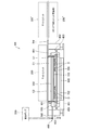
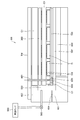
- FIG. 1 is a side view showing a schematic configuration of a semiconductor device inspection apparatus according to a first embodiment of the present invention, taken along line AA (b), and taken along line BB (c). It is explanatory drawing which shows schematic structure of the test
- 1 is a partially enlarged view of a semiconductor device inspection apparatus according to a first embodiment of the present invention; It is a disassembled perspective view which shows schematic structure of the test
- the semiconductor device inspection apparatus M1 has a tray unit (semiconductor device mounting) shown in FIGS. 8 and 9 on which a semiconductor device D as an inspection target is mounted.
- An example of a tray) U1 and a tester unit 200 (an example of a device inspection means) that tests electrical characteristics of the semiconductor device D by conducting electrical continuity with the electrode terminals 101 of the semiconductor device D mounted on the tray unit U1.
- a tester mother board TM (an example of a test board) and a contact pin 102 (an example of a conductive means) provided to face the tester mother board TM and corresponding to the arrangement of terminals provided in the tester mother board TM are provided.
- the first contact substrate C1 and the first contact substrate C1 are provided so as to be interchangeable and provided with the semiconductor device D
- a conversion board 300 having a terminal arrangement having an electrode and a wiring structure for electrically connecting both, a conversion board 300 and a tray unit U1
- the contact pins 103 (an example of the conductive means) corresponding to the arrangement of the electrode terminals 101 provided in the semiconductor device D are provided, and the second contact substrate C2 in which the contact pins 103 are directly connected to the semiconductor device D.
- a connection mechanism 400 (connection means) for electrically connecting the semiconductor device D and the tester unit 200 connected to the tester mother substrate TM via the first contact substrate C1, the conversion substrate 300, and the second contact substrate C2. Example).
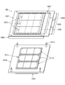
- the semiconductor device mounting tray mounts a plurality of semiconductor devices D as inspection objects, and mounts a plurality of frames 2002 on the tray unit U1.
- the tray unit U1 stores a memory, RFID (IC tag), barcode, etc. (not shown) for storing information (for example, including ID data for identifying the tray unit U1) related to the inspection result by the tester unit 200. You may make it prepare.
- RFID IC tag
- barcode etc.
- tray ID identification number
- processing such as replacing a defective product with a non-defective product or classifying a defective product, thereby improving convenience.
- the conductive means may be constituted by a membrane sheet, an anisotropic conductive sheet or the like instead of the contact pin.
- the tester unit 200 may be provided immediately above the tester mother substrate TM as shown in FIG. 2, or may be provided on the front surface side 200 'or the back surface side 200 "of the extension of the tester mother substrate TM.
- the tester unit 200 may be provided outside by connecting a coaxial cable or the like.
- the semiconductor device D is held by the tray unit U1 so that the electrode terminal 101 side included in the semiconductor device D is the upper surface.
- connection mechanism 400 is provided that electrically connects the semiconductor device D and the tester unit 200 connected to the tester mother substrate TM via the first contact substrate C1, the conversion substrate 300, and the second contact substrate C2. Yes.
- connection mechanism 400 includes a placement portion 401 on which the tray unit U1 is placed, and an actuator (for example, an air cylinder or the like) that raises and lowers the placement portion 401 with respect to the second contact substrate C2.
- an actuator for example, an air cylinder or the like
- connection mechanism 400 includes the lifting / lowering means 402 provided on both sides of the mounting portion 401 and the semiconductor device D when the mounting portion 401 is raised to a predetermined position by the lifting / lowering means 402.
- the electrode terminal 101 and the contact substrate C2 are configured by a vacuum pump 500 (an example of a decompression unit) that sucks negative pressure so that the contact substrate C2 is in close contact.
- the decompression means is provided in the contact substrate frame 403 surrounding the second contact substrate C2, or is provided at the end of the mounting portion 401, and when the mounting portion 401 is raised, the contact substrate frame 403 or A decompression chamber 550 is formed by the seal member 404 that is in contact with the placement unit 401, the contact substrate frame 403, the first contact substrate C 1, the placement unit 401, and the seal member 404, and the atmosphere in the decompression chamber 550 Is sucked by a vacuum pump 500.
- the vacuum pump 500 includes a pressure reducing valve 560 that adjusts the amount of pressure reduction.
- the surface of the semiconductor device D and the upper surface of the tray unit U 1 are pressed down to apply preload to the seal member 404, and then the pressure reducing valve 560 connected to the vacuum pump 500.
- the decompression chamber 550 is decompressed, the semiconductor device D and the tray unit U1 are further pressed by the hot plate 701, and the second contact substrate C2, the conversion substrate 300, and the second contact substrate C2 become the tester mother substrate. All contacts between the semiconductor device D and the tester mother substrate TM which are pressurized by TM and stored in the tray unit U1 are collectively connected with a predetermined force.
- the semiconductor device inspection apparatus M1 it is possible to flexibly cope with a semiconductor device D having a different terminal arrangement or a semiconductor device D having a different configuration, thereby improving the test efficiency and performing the test. Cost can be reduced.
- the decompression means is not limited to the above configuration, and the semiconductor device D and the tester mother substrate TM are brought into close contact with each other via the first contact substrate C1, the conversion substrate 300, and the second contact substrate C2. Any structure can be adopted as long as the structure can be connected to each other.
- alignment holes 600 are formed at a plurality of positions (four corners in the example shown in FIGS. 1 to 3) at the corners of the base plate 2001 of the tray and are extended downward from the tester mother substrate TM. Are engaged for alignment (see FIGS. 1A, 3 and 4).
- the semiconductor device inspection apparatus M1 further includes temperature adjusting means for adjusting the ambient temperature of the semiconductor device D mounted in each tray unit U1 to a predetermined test environment temperature.
- the temperature adjusting means is, for example, disposed below the tray base plate 2001 and includes a heat source 800 such as a Peltier module or a heater via a heat transfer plate 700 and a heat plate 702. .
- a heat source 800 such as a Peltier module or a heater via a heat transfer plate 700 and a heat plate 702. .
- the heat transfer plate 700 is formed of aluminum, copper, stainless steel, brass plate or the like having a thickness of about several millimeters.
- the heat source 800 may be a refrigerant or a heat medium supplied from a chiller, LN2, or the like, or may be a combination of cooling and heating by a Peltier module, a heater, a refrigerant (including LN2), and a heat medium.
- the temperature adjusting means having such a configuration, it is possible to easily adjust the test environment temperature without accommodating the tray unit U1 in a constant temperature bath or the like as in the prior art, improving convenience and increasing the speed of the test. And the test cost can be reduced.
- thermoelectric module As the heat source 800, a high temperature test and a low temperature test, or a cycle test between a high temperature and a low temperature can be easily realized.
- symbol 900 is a receiving part which supports tray unit U1 from the downward direction.
- the second contact substrate C2 and the conversion substrate 300 are exchanged so as to correspond to the characteristics (terminal arrangement, configuration, etc.) of the semiconductor device D to be inspected.
- the tray unit U1 on which the semiconductor device D to be inspected is mounted is set on the placement unit 401.
- the elevating means 402 is operated, and the tray unit U1 is raised together with the placement unit 401.
- the vacuum pump 500 When the predetermined height is reached, the vacuum pump 500 is driven, and the atmosphere in the decompression chamber 550 is sucked.
- the electrode terminal 101 provided in the semiconductor device D, the first contact substrate C1, the second contact substrate C2, the conversion substrate 300, and the tester mother substrate TM are brought into close contact and electrically connected.
- the inspection process of each semiconductor device D is executed by the operation of the tester mother substrate TM and the tester unit 200.
- the contact substrate C2 and the conversion substrate 300 are replaced with corresponding ones, and then the inspection is performed according to the above-described procedure.
- the semiconductor device inspection apparatus M1 it is possible to flexibly cope with a semiconductor device D having a different terminal arrangement or a semiconductor device D having a different configuration, thereby improving the test efficiency and performing the test. Costs can be reduced.
- tray units U1 on which a plurality of semiconductor devices D to be inspected are mounted in parallel are used, and terminals provided in the semiconductor device D are provided on each tray unit U1 on the upper surface side.
- a test board (one example of device inspection means: not shown in FIG. 8) for collectively testing the electrical characteristics of each semiconductor device D in a state of being mounted towards the tray, and the tray unit U1 is made of a metal such as aluminum.
- each frame 2002a, 2002b, 2002c is moved in the horizontal direction with respect to the base plate 2001 (for example, in the direction of arrow A) until positioning by a positioning device (see FIGS. 5 to 12) provided separately is performed. It is a so-called floating structure that is held in a state in which the movement is allowed within a predetermined range (for example, a range until contact with the corner of the alignment hole 2003 shown in FIG. 9C).
- the constituent material of the base plate 2001 is not limited to aluminum, but a material having a thermal conductivity of 100 W / (m ⁇ K) or more is preferable.
- the frame is divided into three.
- the present invention is not limited to this, and the frame may be divided into any number of two or more.
- Alignment holes 2003 are formed at the edges of the frames 2002a, 2002b, and 2002c for aligning the frames 2002a, 2002b, and 2002c with a contact substrate (not shown).
- Alignment holes 2005 are formed in the four corners of the base plate 2001 to align the entire tray unit U1.
- Alignment holes 2003 and alignment holes 2005 are engaged with corresponding alignment pins (see FIG. 7) in the apparatus to align the respective members.
- two frames 2002 are provided horizontally on one tray unit U1.
- a plurality of semiconductor devices D are mounted on each frame 2002 with the terminals facing upward.
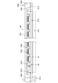
- each frame 2002 In the upper and lower peripheral portions of each frame 2002, three alignment holes 2003 and three floating holes 2004 are provided.
- Alignment hole 2003 and floating hole 2004 have an oval shape formed along the direction of arrow A as shown in FIGS.
- the contact substrate 1022 is provided with an alignment pin 1024 that is inserted into the alignment hole 2003.
- the shape of the alignment pin 1024 is not particularly limited.
- the alignment pin 1024 has a cross-sectional shape (radial cross-sectional shape) similar to the oval shape of the alignment hole 2003. .
- the alignment hole 2003 which is an alignment hole, has an oval shape along a predetermined direction (here, the direction of arrow A), and the alignment hole 2003
- An alignment pin 1024 that is an alignment pin inserted through the hole has a cross-sectional shape similar to that of the alignment hole 2003.
- the alignment hole 2003 may have various shapes other than an oval shape, for example, a circle, an ellipse, and a rectangle.
- the alignment pin 1024 inserted into the alignment hole 2003 is used for alignment. Even if it is a shape that is not similar to the hole 2003, any shape that fits into the alignment hole 2003 and restricts free movement may be used.
- two orthogonal projections 2006 for guiding the semiconductor device D are provided at predetermined positions where the semiconductor device D on the upper part of the base plate 2001 is accommodated. ing.
- each frame 2002 moves in the direction of the arrow A due to the engagement between the alignment pin 1024 and the alignment hole 2003 (FIG. 8 to FIG. 8).
- the semiconductor device mounted on the frame 2002 is also moved in the same direction and pressed against two orthogonal projections 2006 provided on the base plate 2001, so that a gap between the semiconductor device D and the frame 2002 is obtained. (See FIGS. 10 to 12), high-accuracy alignment is performed.
- each frame 2002 is returned in the direction opposite to the arrow A by the elastic force of the leaf spring 2009, and the semiconductor device D is also simultaneously returned to the original position.
- a fixing hole 2008 is formed in the base plate 2001, a floating pin 2007 is inserted through the hole for floating 2004, and a tip portion is press-fitted into the fixing hole 2008 to be fixed ((( see c)).
- the semiconductor device inspection apparatus M2 conducts electrical continuity with the tray unit U1 and the electrode terminal 2010 (see FIGS. 10 to 12) of the semiconductor device D mounted on the tray unit U1 to thereby determine the electrical characteristics of the semiconductor device D.
- a semiconductor device provided in the tray unit U1 provided between a test board 1021 connected to a test unit to be tested (an example of device inspection means: not shown) and a frame constituting the test board 1021 and the lower vacuum chamber 1010
- a contact substrate 1022 provided with a wiring structure (conductive means) for electrically connecting the electrode terminal 2010 of each semiconductor device D mounted on the mounting tray 2002 and the electrode terminal included in the test board 1021, and the contact substrate 1022 Connected to semiconductor device D and test board 1021 And a connection mechanism for electrically connecting (see FIGS. 5 to 7) was a test unit.
- test board 1021 can be replaced according to the type of the semiconductor device D or the arrangement of the electrode terminals 2010 provided in the semiconductor device D.
- the tray unit U1 is installed on the base plate 1010 of the lower vacuum chamber, and then alignment is performed by the alignment pins 1023 of the contact substrate 1022 and the alignment holes 2005 of the base plate 2001 of the tray. Thereby, the position of the tray unit U1 is determined.
- alignment is performed by the alignment holes 2003 on the divided frame 2002 and the alignment pins 1024 provided on the contact substrate 1022.
- a mechanism for pressing the frame 2002 itself in the direction of arrow A may be provided outside the frame 2002. Good.
- Numeral 1004 indicates a mounting area for various circuit members and connection connectors.
- an edge connector 1005 may be provided on one side of the test board 1021.
- a contact substrate frame (upper vacuum chamber frame) 1006 is provided below the test board 1021.
- a seal member 1012 such as an O-ring is provided around the contact substrate frame 1006.
- the tray unit U1 shown in FIG. 8 is placed on a metal (for example, aluminum) placement portion (lower vacuum chamber 1010).
- guide pins 1014 that are inserted into the guide holes 1007 on the test board 1021 side are erected.
- a vacuum valve mounting port 1013 is formed in a part of the lower mounting portion base plate 1010.
- a temperature control unit 1015 configured by a heat sink or a heat source is provided below the placement unit base plate.
- tray unit U1 has been described in the semiconductor device inspection apparatus M3 according to the third embodiment, and a description thereof will be omitted.
- a pressure reducing mechanism that sucks negative pressure so that the electrode terminal 2010 and the contact substrate 1022 provided in the semiconductor device D, and the contact substrate 1022 and the test board 1021 are in close contact with each other. (Pressure reduction means) 1000 is provided.
- the decompression mechanism 1000 includes a first decompression chamber 1001 formed by the test board 1021, the contact substrate 1022, and the seal member 1025, and a vacuum valve that sucks the atmosphere in the first decompression chamber 1002.
- a first vacuum pump (not shown) connected to the opening 1016, a contact substrate frame 1006 surrounding the contact substrate 1022, and an end portion of the placement portion 1010 are moved.
- a second decompression chamber 1002 formed by a seal member 1012 interposed between the contact substrate frame 1006 and a vacuum valve attachment port 1013 for sucking the atmosphere in the second decompression chamber 1002.
- a second vacuum pump (not shown).
- the first vacuum chamber 1001 is depressurized by the first vacuum pump, and then the second depressurization chamber 1002 is depressurized by the second vacuum pump.
- a reliable electrical connection between D and the test board 1021 can be made.
- first vacuum pump and the second vacuum pump instead of the first vacuum pump and the second vacuum pump, a single vacuum pump is provided, and the atmosphere in the first decompression chamber 1001 and the second decompression chamber 1002 is sucked by switching valves. May be.
- a bottom plate may be provided in the tray unit U1, and the bottom plate may be made of a material having a thermal conductivity of 100 W / (m ⁇ K) or more.
- the bottom plate is made of copper (thermal conductivity 385 W / (m ⁇ K), specific gravity 8.9 g / cm 3 ) or aluminum (thermal conductivity 200 W / (m ⁇ K), specific gravity 2.7 g / cm 3. ) Or brass (thermal conductivity 105 W / (m ⁇ K), specific gravity 8.7 g / cm 3 ).
- the thermal conductivity of the bottom plate of the tray unit U1 can be increased and the inspection efficiency of the semiconductor device can be improved.
- plate springs 2009 as shown in FIGS. 8 to 12 are provided at a plurality of locations on the base plate 2001 of the tray, and the frame 2002 is urged in the direction opposite to the arrow A direction to return the position. Good.
- protrusions are provided on two sides on the side where the semiconductor device D is to be pressed, but a square hole for restricting the position of the device on the base plate 2001 (not shown). ) May be used.
- a semiconductor device inspection system S1 applies a semiconductor device inspection apparatus M1 according to the present invention to collectively measure the electrical characteristics and the like of a semiconductor device D for each tray unit U1. It comprises a measuring apparatus M10, a semiconductor device tray transfer apparatus M11 that inverts and transfers the semiconductor device D, and a semiconductor device automatic sorter M12 that sorts the quality of the semiconductor device D.
- the semiconductor device measuring apparatus M10 includes a tester unit 200.
- the tray unit U1 transferred from the semiconductor device tray transfer apparatus M11 is preheated by the preheating unit 3001, and then the tray is detected by the semiconductor device inspection apparatus M1 having the configuration shown in FIGS.
- the semiconductor device D mounted on the unit U1 is collectively tested for electrical characteristics.
- the tray unit U1 is transferred to the heat removal unit 3002, removed heat, and then transferred to the semiconductor device tray transfer device M11.
- the tray unit U1 is transferred to the semiconductor device measurement apparatus M10 in the process of the pre-test shipping tray ⁇ the tray transfer of the semiconductor device D ⁇ the tray handling apparatus 3003, and the test tray is transferred to the semiconductor device measurement apparatus M10.
- the tray unit U1 returned from the tray handling device 3004 ⁇ inversion and transfer of the semiconductor device D ⁇ transfer to the semiconductor device automatic sorter M12 in the process of the shipping tray after the test, or the tray handling device 3004 ⁇ semiconductor device D tray transfer ⁇ Transfer in empty test tray flow.
- the semiconductor device D transferred through the post-test shipping tray is removed based on the inspection result, the defective product is removed, the non-defective product is filled, and the non-defective product shipping tray is followed. Sort D based on test results.
- the tray unit U1 when the tray unit U1 is provided with a memory for storing identification information, an RFID (IC tag), or a barcode, the defective products are classified based on the information. It may be.
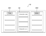
- the semiconductor device inspection system S2 may have a multi-stage structure in which test stages to which the semiconductor device inspection apparatus M1 is applied are stacked over 1 to N (N is an integer) stages.
- a semiconductor device inspection apparatus and a semiconductor device inspection system using the inspection apparatus according to the present invention can be applied to various semiconductor device inspection apparatuses that require a characteristic test.
- SDRAM Secure Digital RAM
- static RAM static RAM
- flash memory logic
- semiconductor devices such as devices and mixed logic / analog devices can be applied as test targets.
- Electrode terminal 102 Contact pin 103 Contact pin 200 Tester unit 300 Conversion board 400 Connection mechanism 401 Mounting part 402 Lifting means 403 Contact board frame 404 Seal member 500 Vacuum pump 550 Pressure reducing chamber 560 Pressure reducing valve 600 Positioning hole 601 Alignment pin 700 Heat transfer plate 701 Heat plate 702 Heat plate 800 Heat source 900 Receiving unit 1000 Pressure reducing mechanism 1001 First pressure reducing chamber 1002 Second pressure reducing chamber 1004 Circuit component and coaxial connector mounting area 1005 Edge connector 1006 Contact substrate frame 1007 Guide hole 1010 Base plate (Lower vacuum chamber) 1012 Seal member 1013 Vacuum valve mounting port 1014 Guide pin 1015 Temperature control unit 1016 Vacuum valve mounting port 1021 Test board (tester mother board) 1022 Contact substrate 1023 Alignment pin (between contact substrate and tray unit) 1024 Pin for alignment (between contact substrate and semiconductor mounting tray) 1025 Seal member 1026 Terminal 2001 Base plate 2002 Frame (divided semiconductor device mounting tray) 2003 Alignment hole (between contact substrate and semiconductor mounting tray) 2004 Floating hole 2005
Landscapes
- Engineering & Computer Science (AREA)
- Computer Hardware Design (AREA)
- Microelectronics & Electronic Packaging (AREA)
- General Engineering & Computer Science (AREA)
- Physics & Mathematics (AREA)
- General Physics & Mathematics (AREA)
- Testing Of Individual Semiconductor Devices (AREA)
- Container, Conveyance, Adherence, Positioning, Of Wafer (AREA)
Abstract
検査対象としての半導体デバイスを複数個にわたって搭載可能とされたトレーユニットであって、底部を形成する底板部材と、該底板部材の上に載置され、且つ水平方向に複数に分割され、それぞれが複数個の前記半導体デバイスを搭載保持する半導体デバイス搭載トレーとを有し、前記半導体デバイスが備える端子を上面側に向けた状態で各半導体デバイスの電気的特性を一括して試験する半導体デバイスの検査装置に着脱自在に載置される。
Description
本発明は半導体デバイスの各種特性試験を行うためのトレーユニットおよび半導体デバイスの検査装置に関するものである。
従来から、試験対象としての半導体デバイスに目的とする高温または低温の温度ストレスを与える半導体デバイスの検査装置が存在する。
半導体デバイスの検査装置としては、例えば、半導体デバイスに対して高温または低温の温度ストレスを与える恒温槽と、この恒温槽で熱ストレスが与えられた状態にある半導体デバイスをテストヘッドに電気的に接触させて電気的特性を試験するテストチャンバと、テストチャンバで試験された半導体デバイスから、与えられた熱ストレスを除去する除熱槽を備えるものがある。
このような半導体デバイスの検査装置では、複数個の半導体デバイスを同時に試験するために、半導体デバイスを搭載する複数個のソケットを取付けたソケットボードを用いている。
このようなソケットボードを用いた半導体デバイスの検査装置に関する技術は種々提案されている。
例えば、特開2000-304808号公報には、一度に検査を行なうことができる半導体装置の数を増加させると共に検査装置のコストを低減し、また、検査工程を安定して行なうことができるようにした半導体装置の検査装置が開示されている。
この半導体装置の検査装置では、プリント基板の上には、ヒータ、多層配線基板及び異方導電性ゴムシートが順次設けられ、異方導電性ゴムシートの上には、半導体パッケージの多層配線基板に対する位置を規制する位置規制部材が配置され、位置規制部材の上方には押圧部材を有する押圧板が設けられ、該押圧板の周縁部には環状のシール部材が設けられ、押圧板、シール部材及び多層配線基板によって密封空間が形成され、密封空間を減圧すると、シール部材が変形して、半導体パッケージのバンプと多層配線基板の電極とが異方導電性ゴムシートを介して電気的に確実に接続するようになっている。
また、特開2007-309787号公報には、ICトレーに搭載されている全ての半導体デバイスをテスト容易な専用トレーに一括に移し変える事が可能なテストトレー構造が開示されている。
ところで、近年の半導体デバイスはその高密度化及び回路の複雑化に伴って一つの半導体デバイスの試験に要する時間が長くなる傾向にあり、テストコストの低廉化のために半導体デバイス試験の一層の効率化が望まれている。
また、半導体デバイスについて多品種の少量生産の傾向が強くなっているため、半導体デバイスの種類に応じて温度条件等の試験環境を頻繁に変更する必要性が高まっている。
しかしながら、上記特開2000-304808号公報に係る従来技術では、配線基板(コンタクト基板)は固定されており、端子配列の異なる半導体デバイスに迅速に対応することができないという問題があった。
また、半導体デバイスの構成毎に端子配列が異なるため、従来は、各半導体デバイスの構成毎に端子配列に適合させたソケットやソケットボードを用意する必要がありコストが嵩むという不都合があった。
また、検査用ピンの数の増加に伴ってソケット自体が高価になり、検査装置のコストや検査コストが高騰化するという問題もある。特に、微細化、高集積化等によりテストに長時間を要するデバイスも増加しており、検査効率の低下および検査コストの上昇は大きな問題になる。
また、近年の半導体デバイスのバーンインテストおよびファイナルテストは、ハンドラーと呼ばれる自動機によりトレーからバーンインボード上のソケットに移し替え、或いはテスターのキャリアボード上のキャリアソケットに移し替え、バーンイン槽或いはテストハンドラーのテストステージで検査を実施している。
そのため、一度に検査を実可能な処理数量の限界および高価で多量に使用するソケットやボード等によるテストコストの増大が大きな課題になっている。
また、ロジックの一部では組立工程ラインでテストを実施されているが、メモリを含めた多くのデバイスの検査は検査専用工程が設けられ、且つ専用のテストハンドラーと一体のシステムが使用され、効率的な生産ラインが実現できていないという課題もある。
一方、比較対象としての半導体デバイスを載せるトレー(ICトレー)では、半導体デバイスの搭載部を構成する樹脂部と、この樹脂部を載せる比較的熱伝導性の高い金属で形成されるベース板とから構成されていた。
また、半導体デバイスとテストボードとの電気的接続を行うコンタクト基板とのアライメントは、例えばトレーの四隅に形成される位置決め用の孔を介して行われていた。
しかしながら、樹脂と金属の線膨張率の違い、比較的薄い樹脂板で成形される場合に樹脂部に熱変形が生じ易いという問題に加え、トレーのデバイスを収容する孔とデバイスの外形の隙間により、高精度の位置合わせが難しいという問題があった。
特に、基板及びトレーの長さが例えば300mm程度と比較的大きい場合、コンタクト基板の端子とトレー内の半導体デバイスの端子の位置合わせ(アライメント手段)が難しいという問題あり、且つトレーとトレー内の半導体デバイス間の隙間のばらつきの抑え手段が無く、高精度の位置合わせが難しいという問題もあった。
そこで、本発明は、半導体デバイスをより効率的且つ低コストで試験することができ、トレーにおける位置合わせの精度を向上させることのできるトレーユニットおよび半導体デバイスの検査装置を提供することを目的とする。
上記課題を解決するために、請求項1の発明に係るトレーユニットは、検査対象としての半導体デバイスを複数個にわたって搭載可能とされたトレーユニットであって、底部を形成する底板部材と、該底板部材の上に載置され、且つ水平方向に複数に分割され、それぞれが複数個の前記半導体デバイスを搭載保持する半導体デバイス搭載トレーとを有し、前記半導体デバイスが備える端子を上面側に向けた状態で各半導体デバイスの電気的特性を試験する半導体デバイスの検査装置に着脱自在に載置され、前記各半導体デバイス搭載トレーは、別途設けられる位置決め手段による位置決めが行われるまでは、前記底板部材に対して水平方向の移動を所定範囲で許容した状態で保持され、前記底板部材の上面には、半導体デバイスの直交する2辺の位置を規制する突起部、或いは半導体デバイスの移動を規制する角穴を持ち、前記半導体デバイストレーを所定の方向に押圧すると同時に半導体デバイスも同方向に移動され、前記底板部材に設けられる直交する2辺の突起に押し付けられることで前記半導体デバイスと前記半導体デバイス搭載トレーとの隙間を無くす手段を備え、前記位置決め手段は、前記半導体デバイス搭載トレーに設けられた位置合わせ用の孔と、前記半導体デバイス搭載トレーと対向して設けられるコンタクト基板側に設けられ、前記位置合わせ用の孔に嵌り込んで前記半導体デバイス搭載トレーと前記コンタクト基板との位置決めを行う位置合わせ用のピンと、前記位置合わせ用のピンを前記位置合わせ用の孔から抜いた際に、弾発力によって前記半導体デバイス搭載トレーを前記所定の方向と反対方向の元の位置に復帰させる押圧手段とを備えることを特徴とする。
請求項2の発明に係る半導体デバイスの検査装置は、請求項1に記載のトレーユニットを載置する載置部と、前記トレーユニットに搭載された半導体デバイスの電極端子と電気的導通を行って前記半導体デバイスの電気的特性を試験するデバイス検査手段に接続されたテストボードと、前記テストボードと前記半導体デバイス搭載トレーとの間に設けられ、前記トレーユニットが備える半導体デバイス搭載トレーに搭載された各半導体デバイスの電極端子と前記テストボードが備える電極端子とを電気的に接続させる導電手段が設けられたコンタクト基板と、前記コンタクト基板を介して前記半導体デバイスと前記テストボードに接続された前記デバイス検査手段とを電気的に接続させる接続機構とを備え、前記接続機構は、前記載置部の両側に設けられる昇降手段と、該昇降手段により前記載置部が所定位置まで相対移動された際に、前記半導体デバイスが備える端子と前記コンタクト基板、当該コンタクト基板と前記テストボードとがそれぞれ密着するように負圧吸引する減圧手段とから構成され、前記減圧手段は、前記コンタクト基板を囲むコンタクト基板枠上の周囲に設けられる、或いは前記載置部の端部に設けられるシール部材と当該載置部が移動された際に前記コンタクト基板枠或いは前記載置部に当接されるシール部材と、前記コンタクト基板枠、前記コンタクト基板、前記載置部および前記シール部材とによって形成される減圧チャンバ内の雰囲気を吸引する真空ポンプと、から構成されることを特徴とする。
本発明によれば以下の効果を奏することができる。
すなわち、請求項1に記載の発明によれば、半導体デバイス搭載トレーを用いて搭載した各半導体デバイスの電気的特性を試験するので、試験効率を向上させることができ、試験コストを低廉化させるという優れた効果を奏することができる。
また、トレーユニットは、底部を形成する底板部材と、該底板部材の上に載置され、且つ水平方向に複数に分割され、それぞれが半導体デバイスを複数個にわたって保持する半導体デバイス搭載トレーとから構成されるので、熱変形等を抑制して半導体デバイスとデバイス検査手段との電気的接続をより確実に行うことができる。
また、請求項1に記載の発明によれば、各半導体デバイス搭載トレーは、位置決め手段による位置決めが行われるまでは、底板部材に対して水平方向の移動を所定範囲で許容した状態で保持される所謂フローティング構造となっているので、位置決め手段による位置決めの精度を向上させることができる。
さらに、請求項1に記載の発明によれば、トレーと半導体デバイス間の隙間が無くなる状態で位置合わせが出来るため、より一層の位置合わせ精度を向上させて、電気的な接続をより確実に行うことができる。
請求項1に記載の発明によれば、簡易な構成で半導体デバイスが備える端子とコンタクト基板と位置合わせ精度を向上させて、電気的な接続をより確実に行うことができる。
請求項1に記載の発明によれば、簡易な構成で半導体デバイス搭載トレーを元の位置に復帰させることができる。
請求項2に記載の発明によれば、端子配列が異なる半導体デバイスや構成の異なる半導体デバイスに対応することができ、試験効率を高めると共に試験コストを低廉化することができるという効果がある。
また、請求項2に記載の発明によれば、半導体デバイスが備える端子とコンタクト基板との電気的な接続を確実に行うことができる。
以下、本発明を実施するための最良の形態を、図面を参照しつつさらに具体的に説明する。ここで、添付図面において同一の部材には同一の符号を付しており、また、重複した説明は省略されている。なお、ここでの説明は本発明が実施される最良の形態であることから、本発明は当該形態に限定されるものではない。
図1から図3等に示される第1の実施の形態に係る半導体デバイスの検査装置M1は、検査対象としての半導体デバイスDが搭載される図8,図9で示されるトレーユニット(半導体デバイス搭載トレーの一例)U1と、トレーユニットU1に搭載された半導体デバイスDの電極端子101と電気的導通を行って半導体デバイスDの電気的特性を試験するテスタユニット200(デバイス検査手段の一例)が搭載されたテスタマザー基板TM(テストボードの一例)と、テスタマザー基板TMに対向して設けられ、テスタマザー基板TMが備える端子の配列に対応したコンタクトピン102(導電手段の一例)が設けられた第1のコンタクト基板C1と、第1のコンタクト基板C1に対向して交換可能に設けられ、半導体デバイスDが備える電極端子101の配列とテスタマザー基板TMが備える端子の配列の相違に対応させて双方を電気的に接続させる電極および配線構造を有する端子配列の変換基板300と、変換基板300とトレーユニットU1との間に設けられ、半導体デバイスDが備える電極端子101の配列に対応したコンタクトピン103(導電手段の一例)が設けられ、当該コンタクトピン103が直接半導体デバイスDと導通する第2のコンタクト基板C2と、第1のコンタクト基板C1、変換基板300および第2のコンタクト基板C2を介して半導体デバイスDとテスタマザー基板TMに接続されたテスタユニット200とを電気的に接続させる接続機構400(接続手段の一例)とを備える。
半導体デバイス搭載トレー(フレーム2002)は、検査対象としての半導体デバイスDを複数個にわたって搭載し、トレーユニットU1に複数個のフレーム2002を搭載するようになっている。
なお、トレーユニットU1は、テスタユニット200による検査結果に関する情報(例えば、トレーユニットU1を識別するIDデータ等を含む)を格納するメモリ、RFID(ICタグ)或いはバーコードなど(図示せず)を備えるようにしてもよい。
これにより、例えばトレーのID(識別番号)に基づいて、不良品を良品に入れ替えたり、不良品を分類するなどの処理を行うことができ、利便性を向上させることができる。
また、コンタクトピンに代えて、メンブレンシート、異方性導電シート等で前記導電手段を構成するようにしてもよい。
テスタユニット200は、図2に示すようにテスタマザー基板TMの直上に設けてもよいし、テスタマザー基板TMの延長部の表面側200’または裏面側200’’に設けるようにしてもよい。
また、テスタユニット200は、同軸ケーブル等の接続で外部に設けるようにしてもよい。
また、本実施の形態において、半導体デバイスDは、当該半導体デバイスDが備える電極端子101側が上面となるようにトレーユニットU1に保持されている。
また、第1のコンタクト基板C1、変換基板300および第2のコンタクト基板C2を介して半導体デバイスDとテスタマザー基板TMに接続されたテスタユニット200とを電気的に接続させる接続機構400を備えている。
本実施の形態において、接続機構400は、トレーユニットU1を載置する載置部401と、当該載置部401を第2のコンタクト基板C2に対して昇降させるアクチュエータ(例えば、エアシリンダ等で構成される昇降手段402)とを備える。
さらに、本実施の形態において接続機構400は、載置部401の両側に設けられる昇降手段402と、この昇降手段402により載置部401が所定位置まで上昇された際に、半導体デバイスDが備える電極端子101とコンタクト基板C2とが密着するように負圧吸引する真空ポンプ500(減圧手段の一例)とから構成されている。
また、減圧手段は、第2のコンタクト基板C2を囲むコンタクト基板枠403に設けられ、或いは載置部401の端部に設けられて当該載置部401が上昇された際にコンタクト基板枠403或いは載置部401に当接されるシール部材404と、コンタクト基板枠403、第1のコンタクト基板C1、載置部401およびシール部材404とによって減圧チャンバ550が形成され、この減圧チャンバ550内の雰囲気を真空ポンプ500で吸引するようになっている。
なお、真空ポンプ500は、減圧量を調整する減圧弁560を備えている。
即ち、コンタクト基板枠403を昇降手段402で加圧することにより、半導体デバイスDの表面およびトレーユニットU1の上面を押し下げ、シール部材404に予圧を加えた後、真空ポンプ500に接続された減圧弁560をオンすることにより、減圧チャンバ550が減圧され、半導体デバイスDとトレーユニットU1がさらに熱板701により押圧され、第2のコンタクト基板C2、変換基板300及び第2のコンタクト基板C2がテスタマザー基板TMに加圧され、トレーユニットU1に収納された半導体デバイスDとテスタマザー基板TM間の全コンタクトが所定の力で一括接続される。
このように、本実施の形態に係る半導体デバイスの検査装置M1によれば、端子配列が異なる半導体デバイスDや構成の異なる半導体デバイスDに機動的に対応することができ、試験効率を高めると共に試験コストを低廉化することができる。
なお、減圧手段は、上記構成に限定されるものではなく、第1のコンタクト基板C1、変換基板300および第2のコンタクト基板C2を介して半導体デバイスDとテスタマザー基板TMとを密着させて電気的に接続させることのできる構造であれば採用できる。
また、トレーのベース板2001のコーナーには、位置決め用の孔600が複数箇所(図1から図3に示す例では4隅)に形成され、テスタマザー基板TMから下方に延伸されるアライメントピン601が係合されて位置合わせを行うようになっている(図1(a)、図3、図4等参照)。
また、半導体デバイスの検査装置M1は、各トレーユニットU1に搭載された半導体デバイスDの周囲温度を所定の試験環境温度に調整する温度調整手段をさらに備えている。
本実施の形態において、温度調整手段は、例えば、トレーのベース板2001の下方に配設され、伝熱プレート700、熱板702を介してペルチェモジュールやヒータ等の熱源800等で構成されている。
なお、特には限定されないが、伝熱プレート700は厚さ数ミリメートル程度のアルミニウム、銅、ステンレス、黄銅板等で形成される。
また、熱源800は、チラーから供給される冷媒又は熱媒、或いはLN2などとしてもよいし、あるいはペルチェモジュール、ヒータ、冷媒(LN2含む)及び熱媒による冷却と加熱を組み合わせてもよい。
このような構成の温度調整手段により、従来のように恒温槽等にトレーユニットU1を収容することなく、簡便に試験環境温度を調整することができ、利便性が向上され試験の高速化が図られると共に、試験コストを低廉化することができる。
また、熱源800としてペルチェモジュールを実装することにより、高温テスト及び低温テスト、或いは高温と低温との間のサイクルテストを容易に実現することができる。
なお、符号900は、トレーユニットU1を下方から支持する受部である。
次に、本実施の形態に係る半導体デバイスの検査装置M1の動作について説明する。
まず、半導体デバイスの検査装置M1において、検査対象としての半導体デバイスDの特性(端子配列、構成等)に対応するように、第2のコンタクト基板C2および変換基板300を交換する。
次いで、検査対象としての半導体デバイスDを搭載したトレーユニットU1を載置部401にセットする。
続いて、昇降手段402が作動され、トレーユニットU1が載置部401ごと上昇される。
そして、所定の高さに達すると、真空ポンプ500が駆動され、上述の減圧チャンバ550内の雰囲気が吸引される。
これにより、半導体デバイスDが備える電極端子101と、第1コンタクト基板C1、第2のコンタクト基板C2、変換基板300、テスタマザー基板TMとが密着され、電気的に接続される。
次いで、温度調整手段により半導体デバイスDが所定の温度まで加熱または冷却された後、テスタマザー基板TMおよびテスタユニット200の動作によって各半導体デバイスDの検査処理が実行されることとなる。
また、他の構成の半導体デバイスを検査する場合には、コンタクト基板C2および変換基板300を対応するものに交換した後、上述の手順で検査を行う。
このように、本実施の形態に係る半導体デバイスの検査装置M1によれば、端子配列が異なる半導体デバイスDや構成の異なる半導体デバイスDに機動的に対応することができ、試験効率を高めると共に試験コストを低廉化することが可能となる。
なお、本実施の形態では、半導体デバイスDの端子を上向きにした場合を示したが、半導体デバイスDの端子を下向きにした場合にも本発明を適用することが可能である。
次に、図8から図12を参照して、第3の実施の形態に係る半導体デバイスの検査装置M3について説明する。
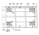
半導体デバイスの検査装置M3では、検査対象としての半導体デバイスDを複数個にわたって並列状態で搭載する1または2以上のトレーユニットU1を用い、各トレーユニットU1に、半導体デバイスDが備える端子を上面側に向けて搭載した状態で各半導体デバイスDの電気的特性を一括して試験するテストボード(デバイス検査手段の一例:図8には現れない)を備え、トレーユニットU1は、アルミニウム等の金属で形成される底板部材(ベース板)2001と、このベース板2001の上に載置され、且つ水平方向に複数に分割され、それぞれが半導体デバイスDを複数個にわたって保持する半導体デバイス搭載トレー(例えば樹脂あるいは金属で形成されるフレーム)2002a、2002b、2002cとから構成される。
また、各フレーム2002a、2002b、2002cは、別途設けられる位置決め装置(図5~図12参照)による位置決めが行われるまでは、ベース板2001に対して水平方向の移動(例えば、矢印A方向への移動)を所定範囲(例えば、図9の(c)で示すアライメント用の孔2003の隅部に接触するまでの範囲)で許容した状態で保持される所謂フローティング構造とされている。
また、ベース板2001の構成材料は、アルミニウムに限らないが、熱伝導率が100W/(m・K)以上の材料が好ましい。
なお、本実施の形態では、フレームを3つに分割しているが、これに限定されず、2以上であれば幾つに分割してもよい。
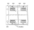
各フレーム2002a、2002b、2002cの縁部には、図示しないコンタクト基板との間で各フレーム2002a、2002b、2002cの位置合わせを行うためのアライメント用の孔2003が穿設されている。
また、ベース板2001の四隅には、トレーユニットU1全体の位置合わせを行うためのアライメント用の孔2005が穿設されている。
アライメント用の孔2003およびアライメント用の孔2005には、装置内において対応するアライメント用のピン(図7参照)が係合して、それぞれの部材の位置合わせを行うようになっている。
これにより、アライメント用のピンにより位置補正を行うことができる。
また、トレーユニットU1における熱変形の抑制を図ることもできる。
また、本実施の形態では、図5~図9に示すように、一つのトレーユニットU1にフレーム2002が横に2個(2002a、2002b、2002c)設けられるようになっている。
また、本実施の形態では、各フレーム2002に、複数個の半導体デバイスD(例えば、DDR3、BGAパッケージ)が、端子を上側に向けた状態で搭載されるようになっている。
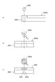
各フレーム2002の上下周辺部には、3つのアライメント用の孔2003と、3つのフローティング用の孔2004が設けられている。
アライメント用の孔2003およびフローティング用の孔2004は、図12の(a)、(b)に示すように矢印A方向に沿って形成される長円形状とされている。
図5~図7に示すように、コンタクト基板1022には、アライメント用の孔2003に挿通されるアライメント用のピン1024が設けられている。
アライメント用のピン1024の形状は、特には限定されないが、例えば図7に示すように、アライメント用の孔2003の長円形状と相似の断面形状(径方向の断面形状)を有するようにされる。
このように本実施の形態では、位置合わせ用の孔であるアライメント用の孔2003は所定の方向(ここでは、矢印A方向)に沿った長円形状を有しており、アライメント用の孔2003に挿通される位置合わせ用のピンであるアライメント用のピン1024はアライメント用の孔2003と相似の断面形状となっている。しかしながら、アライメント用のピン1024がアライメント用の孔2003に嵌り込んで半導体デバイス搭載トレー2002とコンタクト基板1022との位置決めが行えるようになっていれば足りる。したがって、アライメント用の孔2003は長円形状以外の形状、例えば円形、楕円形、矩形など様々な形状であってもよく、このアライメント用の孔2003に挿通されるアライメント用のピン1024はアライメント用の孔2003と相似ではない形状であっても、アライメント用の孔2003に嵌り込んで自由な動きが規制されるような形状であればよい。
図9の(a)、(b)に示すようにベース板2001の上部の半導体デバイスDが収納される所定の位置には半導体デバイスDをガイドするための直交する2辺の突起2006が設けられている。
そして、アライメント用の孔2003にアライメント用のピン1024が挿通されると、アライメント用のピン1024とアライメント用の孔2003との係合により、各フレーム2002が、矢印A方向に移動(図8~図12参照)すると同時にフレーム2002に搭載されている半導体デバイスも同方向に移動され、ベース板2001に設けられた直交する2辺の突起2006に押しつけられることで半導体デバイスDとフレーム2002間の隙間が無くなり(図10~図12参照)精度の高い位置合わせが行われる。
なお、本実施の形態においては、図8および図9に示すように、ベース板2001の所定の位置に、板バネ2009が設けられ、アライメント用のピン1024をアライメント用の孔2003から抜いた際に、板バネ2009の弾発力により各フレーム2002が矢印Aと逆方向に戻って、半導体デバイスDも同時に元の位置に復帰させるようになっている。
一方、ベース板2001には固定孔2008が形成され、フローティングピン2007がフローティング用の孔2004から挿通され、先端部が固定孔2008に圧入されて固定されるようになっている(図12の(c)を参照)。
次に、図4~図12を参照して、第2の実施の形態に係る半導体デバイスの検査装置M2について説明する。
半導体デバイスの検査装置M2は、トレーユニットU1と、トレーユニットU1に搭載された半導体デバイスDの電極端子2010(図10~図12参照)と電気的導通を行って半導体デバイスDの電気的特性を試験するテストユニット(デバイス検査手段の一例:図示せず)に接続されたテストボード1021と、テストボード1021と下部真空チャンバ1010を構成するフレームとの間に設けられ、トレーユニットU1が備える半導体デバイス搭載トレー2002に搭載された各半導体デバイスDの電極端子2010とテストボード1021が備える電極端子とを電気的に接続させる配線構造(導電手段)が設けられたコンタクト基板1022と、コンタクト基板1022を介して半導体デバイスDとテストボード1021に接続されたテストユニットとを電気的に接続させる接続機構(図5~図7参照)とを備えている。
また、テストボード1021は、半導体デバイスDの種類または半導体デバイスDが備える電極端子2010の配列に応じて、交換可能とされている。
次に、本実施の形態に係る半導体デバイスの検査装置M2におけるアライメント動作の概要について説明する。
まず、トレーユニットU1を下部真空チャンバのベース板1010に設置し、次いで、コンタクト基板1022のアライメントピン1023とトレーのベース板2001のアライメント用の孔2005によりアライメントを行う。これにより、トレーユニットU1の位置が決められる。
次に、分割されたフレーム2002上のアライメント用の孔2003とコンタクト基板1022に設けられたアライメント用のピン1024によりアライメントを行う。
そして、最後にコンタクト基板1022の端子1026の先端と半導体デバイスDの電極端子2010との間のアライメントを行う。
これにより、フレーム2002の熱変形等を抑制して半導体デバイスDとテストボードとの電気的接続をより確実に行うことができる。
また、アライメント用のピン1024とアライメント用の孔2003との係合によりフレーム2002を移動させる機構に代えて、フレーム2002の外部にフレーム2002自体を矢印A方向に押圧する機構を設けるようにしてもよい。
次に、図4~図6を参照して、第2の実施の形態に係る半導体デバイスの検査装置M2について説明する。
図4~図6に示すように、上部構成は、テストボード1021の下側には分割された3つのコンタクト基板1022が配置されている。
テストボード1021の四隅には、後述するガイドピン1014が挿通されるガイド孔1007が設けられている。
符号1004は、各種回路部材や接続コネクタの実装領域を示す。
また、テストボード1021の一側方にはエッジコネクタ1005を設けるようにしてもよい。
テストボード1021の下方には、コンタクト基板枠(上部真空チャンバ枠)1006が設けられている。
また、図4~図6に示すように、コンタクト基板枠1006の周囲には、Oリング等のシール部材1012が設けられている。
一方、下部構成は、金属製(例えばアルミ製)の載置部(下部真空チャンバ1010)の上に、前出の図8で示したトレーユニットU1が載置されている。
ベース板1010の四隅には、テストボード1021側のガイド孔1007に挿通されるガイドピン1014が立設されている。
また、下部の載置部ベース板1010の一部には、真空バルブの取付口1013が形成されている。
また、載置部ベース板の下方には、ヒートシンク或いは熱源等で構成される温調部1015が設けられている。
なお、トレーユニットU1の詳細については、第3の実施の形態に係る半導体デバイスの検査装置M3で説明したので省略する。
また、図5~図9に示すように、接続機構として、半導体デバイスDが備える電極端子2010とコンタクト基板1022と、コンタクト基板1022とテストボード1021とがそれぞれ密着するように負圧吸引する減圧機構(減圧手段)1000を備えている。
本実施の形態において、減圧機構1000は、テストボード1021、コンタクト基板1022およびシール部材1025によって形成される第1の減圧チャンバ1001と、第1の減圧チャンバ1002内の雰囲気を吸引する真空バルブの取付口1016に接続される第1の真空ポンプ(図示せず)と、コンタクト基板1022を囲むコンタクト基板枠1006と、載置部1010の端部に設けられて当該載置部1010が移動された際にコンタクト基板枠1006との間に介在されるシール部材1012とによって形成される第2の減圧チャンバ1002と、該第2の減圧チャンバ1002内の雰囲気を吸引する真空バルブの取付口1013に接続される第2の真空ポンプ(図示せず)とから構成される。
そして、特には限定されないが、例えば、まず最初に第1の真空ポンプにより第1の減圧チャンバ1001を減圧し、次いで第2の真空ポンプにより第2の減圧チャンバ1002を減圧することにより、半導体デバイスDとテストボード1021との確実な電気的接続を行うことができる。
また、第1の真空ポンプ、第2の真空ポンプに代えて、一つの真空ポンプを設け、バルブの切り換えによって、第1の減圧チャンバ1001と第2の減圧チャンバ1002内の雰囲気を吸引するようにしてもよい。
また、例えば、トレーユニットU1に底板を設け、この底板を熱伝導率が100W/(m・K)以上の材料で構成するようにしてもよい。
より具体的には、底板を銅(熱伝導率385W/(m・K)、比重8.9g/cm3)またはアルミニウム(熱伝導率200W/(m・K)、比重2.7g/cm3)或いは黄銅(熱伝導率105W/(m・K)、比重8.7g/cm3)で構成するとよい。
これにより、トレーユニットU1の底板の熱伝導率を高めて半導体デバイスの検査効率を向上させることができる。
また、トレーのベース板2001の複数箇所に図8~図12で示すような板バネ2009を設けて、フレーム2002を矢印A方向と反対方向に付勢して、位置を復帰させるようにしてもよい。
また、図9の(a)、(b)では1例として、半導体デバイスDを押し付けたい側の2辺に突起を設けているがベース板2001にデバイスの位置を規制する角穴(図示は省略)を設けるなど他の手段でも良い。
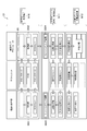
次に、図13、図14を参照して、半導体デバイスの検査システムS1について簡単に説明する。
図13に示すように、半導体デバイスの検査システムS1は、本発明に係る半導体デバイスの検査装置M1を適用してトレーユニットU1ごと一括して半導体デバイスDの電気的特性等の測定を行う半導体デバイス測定装置M10と、半導体デバイスDの反転および移し替えを行う半導体デバイストレー移替装置M11と、半導体デバイスDの良否を選別する半導体デバイス自動選別機M12とから構成されている。
半導体デバイス測定装置M10は、テスタユニット200を備えている。
そして、半導体デバイス測定装置M10では、半導体デバイストレー移替装置M11から移送されたトレーユニットU1を予熱部3001で予熱した後、図1~図3等に示す構成の半導体デバイスの検査装置M1によってトレーユニットU1に搭載された半導体デバイスDについて一括して電気的特性の試験が行われる。
次いで、トレーユニットU1は除熱部3002に移送され、除熱された後に、半導体デバイストレー移替装置M11へ移送される。
半導体デバイストレー移替装置M11において、テスト前出荷トレー → 半導体デバイスDのトレー移替 → トレーハンドリング装置3003の過程で半導体デバイス測定装置M10にトレーユニットU1を移送し、半導体デバイス測定装置M10にテストトレーから戻って来たトレーユニットU1について、トレーハンドリング装置3004 → 半導体デバイスDの反転と移替 → テスト後出荷トレーの過程で半導体デバイス自動選別機M12に移送したり、あるいはトレーハンドリング装置3004 → 半導体デバイスDのトレー移替 → 空テストトレーの流れで移送する。
また、半導体デバイス自動選別機M12では、テスト後出荷トレーを介して移送されて来た半導体デバイスDについて、検査結果に基づいて、不良品の取除き → 良品充填 → 良品出荷トレーの流れで半導体デバイスDをテスト結果に基づき選別する。
なお、取り除いた不良品については、トレーユニットU1に、識別情報等を格納するメモリ、RFID(ICタグ)或いはバーコードを備えるようにした場合に、それらの情報に基づいて不良品を分類するようにしてもよい。
また、半導体デバイスの検査装置M1を適用したテストステージを1~N(Nは整数)段にわたって積み重ねた多段構造を有する半導体デバイスの検査システムS2として構成してもよい。
以上本発明者によってなされた発明を実施の形態に基づき具体的に説明したが、本明細書で開示された実施の形態はすべての点で例示であって開示された技術に限定されるものではないと考えるべきである。即ち、本発明の技術的な範囲は、上記の実施の形態における説明に基づいて制限的に解釈されるものでなく、あくまでも特許請求の範囲の記載に従って解釈すべきであり、特許請求の範囲の記載技術と均等な技術および特許請求の範囲内でのすべての変更が含まれる。
本発明による半導体デバイスの検査装置および当該検査装置を用いた半導体デバイスの検査システムは、特性テストが必要な様々な半導体デバイスの検査装置に適用できるものであり、SDRAM、スタティックRAM、フラッシュメモリ、ロジックデバイス、ロジック・アナログ混載デバイスなど、様々な半導体デバイスをテスト対象として適用することができる。
101 電極端子
102 コンタクトピン
103 コンタクトピン
200 テスタユニット
300 変換基板
400 接続機構
401 載置部
402 昇降手段
403 コンタクト基板枠
404 シール部材
500 真空ポンプ
550 減圧チャンバ
560 減圧弁
600 位置決め用の孔
601 アライメントピン
700 伝熱プレート
701 熱板
702 熱板
800 熱源
900 受部
1000 減圧機構
1001 第1の減圧チャンバ
1002 第2の減圧チャンバ
1004 回路部品及び同軸コネクタ実装域
1005 エッジコネクタ
1006 コンタクト基板枠
1007 ガイド孔
1010 ベース板(下部真空チャンバ)
1012 シール部材
1013 真空バルブの取付口
1014 ガイドピン
1015 温調部
1016 真空バルブの取付口
1021 テストボード(テスタマザー基板)
1022 コンタクト基板
1023 アライメントピン(コンタクト基板とトレーユニット間)
1024 アライメント用のピン(コンタクト基板と半導体搭載トレー間)
1025 シール部材
1026 端子
2001 ベース板
2002 フレーム(分割された半導体デバイス搭載トレー)
2003 アライメント用の孔(コンタクト基板と半導体搭載トレー間)
2004 フローティング用の孔
2005 アライメント用の孔(コンタクト基板とトレーユニット間)
2006 突起
2007 フローティングピン
2008 固定孔
2009 板バネ
2010 半導体デバイスの電極端子
3001 予熱部
3002 除熱部
3003 トレーハンドリング装置
3004 トレーハンドリング装置
C1 第1のコンタクト基板
C2 第2のコンタクト基板
D 半導体デバイス
M1~M3 半導体デバイスの検査装置
M10 半導体デバイス測定装置
M11 半導体デバイストレー移替装置
M12 半導体デバイス自動選別機
S1,S2 検査システム
U1 トレーユニット
Claims (2)
- 検査対象としての半導体デバイスを複数個にわたって搭載可能とされたトレーユニットであって、底部を形成する底板部材と、該底板部材の上に載置され、且つ水平方向に複数に分割され、それぞれが複数個の前記半導体デバイスを搭載保持する半導体デバイス搭載トレーとを有し、前記半導体デバイスが備える端子を上面側に向けた状態で各半導体デバイスの電気的特性を試験する半導体デバイスの検査装置に着脱自在に載置され、
前記各半導体デバイス搭載トレーは、別途設けられる位置決め手段による位置決めが行われるまでは、前記底板部材に対して水平方向の移動を所定範囲で許容した状態で保持され、
前記底板部材の上面には、半導体デバイスの直交する2辺の位置を規制する突起部、或いは半導体デバイスの移動を規制する角穴を持ち、前記半導体デバイストレーを所定の方向に押圧すると同時に半導体デバイスも同方向に移動され、前記底板部材に設けられる直交する2辺の突起に押し付けられることで前記半導体デバイスと前記半導体デバイス搭載トレーとの隙間を無くす手段を備え、
前記位置決め手段は、
前記半導体デバイス搭載トレーに設けられた位置合わせ用の孔と、
前記半導体デバイス搭載トレーと対向して設けられるコンタクト基板側に設けられ、前記位置合わせ用の孔に嵌り込んで前記半導体デバイス搭載トレーと前記コンタクト基板との位置決めを行う位置合わせ用のピンと、
前記位置合わせ用のピンを前記位置合わせ用の孔から抜いた際に、弾発力によって前記半導体デバイス搭載トレーを前記所定の方向と反対方向の元の位置に復帰させる押圧手段とを備える、
ことを特徴とするトレーユニット。 - 請求項1に記載のトレーユニットを載置する載置部と、
前記トレーユニットに搭載された半導体デバイスの電極端子と電気的導通を行って前記半導体デバイスの電気的特性を試験するデバイス検査手段に接続されたテストボードと、前記テストボードと前記半導体デバイス搭載トレーとの間に設けられ、前記トレーユニットが備える半導体デバイス搭載トレーに搭載された各半導体デバイスの電極端子と前記テストボードが備える電極端子とを電気的に接続させる導電手段が設けられたコンタクト基板と、前記コンタクト基板を介して前記半導体デバイスと前記テストボードに接続された前記デバイス検査手段とを電気的に接続させる接続機構とを備え、
前記接続機構は、前記載置部の両側に設けられる昇降手段と、該昇降手段により前記載置部が所定位置まで相対移動された際に、前記半導体デバイスが備える端子と前記コンタクト基板、当該コンタクト基板と前記テストボードとがそれぞれ密着するように負圧吸引する減圧手段とから構成され、
前記減圧手段は、前記コンタクト基板を囲むコンタクト基板枠上の周囲に設けられる、或いは前記載置部の端部に設けられるシール部材と当該載置部が移動された際に前記コンタクト基板枠或いは前記載置部に当接されるシール部材と、前記コンタクト基板枠、前記コンタクト基板、前記載置部および前記シール部材とによって形成される減圧チャンバ内の雰囲気を吸引する真空ポンプと、から構成されることを特徴とする半導体デバイスの検査装置。
Applications Claiming Priority (4)
| Application Number | Priority Date | Filing Date | Title |
|---|---|---|---|
| JP2010-171857 | 2010-07-30 | ||
| JP2010171857 | 2010-07-30 | ||
| JP2010-292784 | 2010-12-28 | ||
| JP2010292784A JP4765127B1 (ja) | 2010-07-30 | 2010-12-28 | トレーユニットおよび半導体デバイスの検査装置 |
Publications (1)
| Publication Number | Publication Date |
|---|---|
| WO2012014899A1 true WO2012014899A1 (ja) | 2012-02-02 |
Family
ID=44693557
Family Applications (1)
| Application Number | Title | Priority Date | Filing Date |
|---|---|---|---|
| PCT/JP2011/066981 WO2012014899A1 (ja) | 2010-07-30 | 2011-07-26 | トレーユニットおよび半導体デバイスの検査装置 |
Country Status (3)
| Country | Link |
|---|---|
| JP (1) | JP4765127B1 (ja) |
| TW (1) | TW201205099A (ja) |
| WO (1) | WO2012014899A1 (ja) |
Cited By (9)
| Publication number | Priority date | Publication date | Assignee | Title |
|---|---|---|---|---|
| EP2871059A1 (en) * | 2013-11-07 | 2015-05-13 | Vistaprint Schweiz GmbH | Conveyance printing system and method for printing on multiple different types of articles of manufacture |
| US9114645B2 (en) | 2012-06-18 | 2015-08-25 | Cimpress Schweiz Gmbh | System and method for printing on multiple different articles of manufacture by the same printing system in a conveyor system |
| US9156293B2 (en) | 2012-06-18 | 2015-10-13 | Cimpress Schweiz Gmbh | Manufacturing tray with customized inlays for processing different types of articles of manufacture |
| GB2539086A (en) * | 2015-04-21 | 2016-12-07 | Keysight Technologies Inc | Portable vacuum chamber and an associated automated test system and method for the testing of electronic devices |
| US9656481B2 (en) | 2012-06-18 | 2017-05-23 | Cimpress Schweiz Gmbh | Integrated imprinting system and trays for selectively processing items on tray |
| JP6178969B1 (ja) * | 2016-08-19 | 2017-08-16 | 合同会社Pleson | トレー交換式バーンイン試験ユニット |
| TWI694263B (zh) * | 2019-03-07 | 2020-05-21 | 雍智科技股份有限公司 | 老化測試電路板模組 |
| CN116679183A (zh) * | 2023-08-03 | 2023-09-01 | 深圳市诺泰芯装备有限公司 | 一种igbt产品的测试方法及装置 |
| TWI825738B (zh) * | 2021-07-22 | 2023-12-11 | 韓商细美事有限公司 | 測試分類機的托盤升降裝置以及測試分類機 |
Families Citing this family (4)
| Publication number | Priority date | Publication date | Assignee | Title |
|---|---|---|---|---|
| KR101611922B1 (ko) * | 2014-05-12 | 2016-04-14 | 참엔지니어링(주) | 기판 검사 장치 및 기판 검사 방법 |
| KR102393040B1 (ko) * | 2015-11-27 | 2022-05-03 | (주)테크윙 | 전자부품 테스트용 결합장치 |
| JP6842355B2 (ja) * | 2017-04-28 | 2021-03-17 | 株式会社アドバンテスト | 電子部品試験装置用のキャリア |
| JP6471401B1 (ja) * | 2017-10-31 | 2019-02-20 | 合同会社Pleson | 半導体ウエハーの試験ユニット |
Citations (4)
| Publication number | Priority date | Publication date | Assignee | Title |
|---|---|---|---|---|
| JPH0572269A (ja) * | 1991-09-10 | 1993-03-23 | Hitachi Electron Eng Co Ltd | Icテスターの測定治具 |
| JPH07260879A (ja) * | 1994-03-25 | 1995-10-13 | Advantest Corp | Ic試験装置のテストヘッド用インターフェイス |
| JP2008039666A (ja) * | 2006-08-09 | 2008-02-21 | Fujitsu Ltd | プローバ装置用搬送トレイ |
| WO2008050443A1 (fr) * | 2006-10-27 | 2008-05-02 | Advantest Corporation | Plateau client et appareil de test de composant électronique |
Family Cites Families (5)
| Publication number | Priority date | Publication date | Assignee | Title |
|---|---|---|---|---|
| JP3825504B2 (ja) * | 1996-07-12 | 2006-09-27 | 株式会社日本マイクロニクス | 集積回路チップ用トレー |
| JP2000304808A (ja) * | 1999-04-23 | 2000-11-02 | Matsushita Electric Ind Co Ltd | 半導体装置の検査装置 |
| JP2005345262A (ja) * | 2004-06-03 | 2005-12-15 | Niigata Seimitsu Kk | 半導体検査装置およびこれに用いる被検査部品トレー |
| JP4715601B2 (ja) * | 2006-04-07 | 2011-07-06 | 住友電気工業株式会社 | 電気接続部品 |
| WO2010021038A1 (ja) * | 2008-08-20 | 2010-02-25 | 株式会社アドバンテスト | 電子部品ハンドリング装置および電子部品試験システム |
-
2010
- 2010-12-28 JP JP2010292784A patent/JP4765127B1/ja not_active Expired - Fee Related
-
2011
- 2011-07-26 WO PCT/JP2011/066981 patent/WO2012014899A1/ja active Application Filing
- 2011-07-29 TW TW100126932A patent/TW201205099A/zh not_active IP Right Cessation
Patent Citations (4)
| Publication number | Priority date | Publication date | Assignee | Title |
|---|---|---|---|---|
| JPH0572269A (ja) * | 1991-09-10 | 1993-03-23 | Hitachi Electron Eng Co Ltd | Icテスターの測定治具 |
| JPH07260879A (ja) * | 1994-03-25 | 1995-10-13 | Advantest Corp | Ic試験装置のテストヘッド用インターフェイス |
| JP2008039666A (ja) * | 2006-08-09 | 2008-02-21 | Fujitsu Ltd | プローバ装置用搬送トレイ |
| WO2008050443A1 (fr) * | 2006-10-27 | 2008-05-02 | Advantest Corporation | Plateau client et appareil de test de composant électronique |
Cited By (12)
| Publication number | Priority date | Publication date | Assignee | Title |
|---|---|---|---|---|
| US9114645B2 (en) | 2012-06-18 | 2015-08-25 | Cimpress Schweiz Gmbh | System and method for printing on multiple different articles of manufacture by the same printing system in a conveyor system |
| US9156293B2 (en) | 2012-06-18 | 2015-10-13 | Cimpress Schweiz Gmbh | Manufacturing tray with customized inlays for processing different types of articles of manufacture |
| US9656481B2 (en) | 2012-06-18 | 2017-05-23 | Cimpress Schweiz Gmbh | Integrated imprinting system and trays for selectively processing items on tray |
| EP2871059A1 (en) * | 2013-11-07 | 2015-05-13 | Vistaprint Schweiz GmbH | Conveyance printing system and method for printing on multiple different types of articles of manufacture |
| GB2539086A (en) * | 2015-04-21 | 2016-12-07 | Keysight Technologies Inc | Portable vacuum chamber and an associated automated test system and method for the testing of electronic devices |
| GB2539086B (en) * | 2015-04-21 | 2018-05-16 | Keysight Technologies Inc | Portable vacuum chamber and an associated automated test system and method for the testing of electronic devices |
| US10031178B2 (en) | 2015-04-21 | 2018-07-24 | Keysight Technologies, Inc. | Portable vacuum chamber and an associated automated test system and method for the testing of electronic devices |
| JP6178969B1 (ja) * | 2016-08-19 | 2017-08-16 | 合同会社Pleson | トレー交換式バーンイン試験ユニット |
| JP2018028524A (ja) * | 2016-08-19 | 2018-02-22 | 合同会社Pleson | トレー交換式バーンイン試験ユニット |
| TWI694263B (zh) * | 2019-03-07 | 2020-05-21 | 雍智科技股份有限公司 | 老化測試電路板模組 |
| TWI825738B (zh) * | 2021-07-22 | 2023-12-11 | 韓商细美事有限公司 | 測試分類機的托盤升降裝置以及測試分類機 |
| CN116679183A (zh) * | 2023-08-03 | 2023-09-01 | 深圳市诺泰芯装备有限公司 | 一种igbt产品的测试方法及装置 |
Also Published As
| Publication number | Publication date |
|---|---|
| JP2012047717A (ja) | 2012-03-08 |
| TW201205099A (en) | 2012-02-01 |
| JP4765127B1 (ja) | 2011-09-07 |
| TWI414802B (ja) | 2013-11-11 |
Similar Documents
| Publication | Publication Date | Title |
|---|---|---|
| JP4765127B1 (ja) | トレーユニットおよび半導体デバイスの検査装置 | |
| JP5690321B2 (ja) | プローブ装置および試験装置 | |
| TWI388841B (zh) | 測試系統以及探針裝置 | |
| JP2016095141A (ja) | 半導体デバイスの検査ユニット | |
| US8212579B2 (en) | Fixing apparatus for a probe card | |
| TWI578001B (zh) | 半導體元件對準插座單元以及含其之半導體元件測試裝置 | |
| JP2011220924A (ja) | 試験装置および接続装置 | |
| KR100383009B1 (ko) | 반도체 집적 회로의 검사 방법, 검사 장치 및 진공 컨택터 기구 | |
| KR102411561B1 (ko) | 온도 측정 부재, 검사 장치 및 온도 측정 방법 | |
| JP2011091262A (ja) | プローバおよびプローブ検査方法 | |
| JP2021009146A (ja) | 半導体パッケージテスト装置 | |
| KR100690514B1 (ko) | 반도체 기판 시험 장치 및 반도체 기판 시험 방법 | |
| TW201842345A (zh) | 電子元件測試裝置用之載具 | |
| JP2010169526A (ja) | 電気的試験用装置及び電子装置の電気的試験方法 | |
| TW522438B (en) | Method for producing semiconductor device | |
| JP7060661B2 (ja) | プレスヘッドロック機構及びプレスヘッドロック機構を有する電子部品検査装置 | |
| KR101025265B1 (ko) | 통전 부재, 접속 부재, 시험 장치 및 접속 부재를 수선하는 방법 | |
| JP2015055511A (ja) | 半導体デバイスの検査ユニット | |
| WO2009130793A1 (ja) | 試験システムおよびプローブ装置 | |
| JP2011237446A (ja) | Ic一括移動方法 | |
| JP6842355B2 (ja) | 電子部品試験装置用のキャリア | |
| KR102198300B1 (ko) | 반도체 소자 테스트 장치 | |
| JP2014107509A (ja) | プローブ装置、試験装置、及び、プローブ方法 | |
| JP2018189391A (ja) | 電子部品試験装置用のキャリア | |
| WO2018035515A1 (en) | Test stack having wafer translator and stiffening interface, and associated systems and methods |
Legal Events
| Date | Code | Title | Description |
|---|---|---|---|
| 121 | Ep: the epo has been informed by wipo that ep was designated in this application |
Ref document number: 11812488 Country of ref document: EP Kind code of ref document: A1 |
|
| NENP | Non-entry into the national phase |
Ref country code: DE |
|
| 122 | Ep: pct application non-entry in european phase |
Ref document number: 11812488 Country of ref document: EP Kind code of ref document: A1 |