WO2011152352A1 - 半導体装置の製造方法及び基板処理装置 - Google Patents
半導体装置の製造方法及び基板処理装置 Download PDFInfo
- Publication number
- WO2011152352A1 WO2011152352A1 PCT/JP2011/062381 JP2011062381W WO2011152352A1 WO 2011152352 A1 WO2011152352 A1 WO 2011152352A1 JP 2011062381 W JP2011062381 W JP 2011062381W WO 2011152352 A1 WO2011152352 A1 WO 2011152352A1
- Authority
- WO
- WIPO (PCT)
- Prior art keywords
- substrate
- processing chamber
- raw material
- gas supply
- gas
- Prior art date
- Legal status (The legal status is an assumption and is not a legal conclusion. Google has not performed a legal analysis and makes no representation as to the accuracy of the status listed.)
- Ceased
Links
Images




Classifications
-
- C—CHEMISTRY; METALLURGY
- C23—COATING METALLIC MATERIAL; COATING MATERIAL WITH METALLIC MATERIAL; CHEMICAL SURFACE TREATMENT; DIFFUSION TREATMENT OF METALLIC MATERIAL; COATING BY VACUUM EVAPORATION, BY SPUTTERING, BY ION IMPLANTATION OR BY CHEMICAL VAPOUR DEPOSITION, IN GENERAL; INHIBITING CORROSION OF METALLIC MATERIAL OR INCRUSTATION IN GENERAL
- C23C—COATING METALLIC MATERIAL; COATING MATERIAL WITH METALLIC MATERIAL; SURFACE TREATMENT OF METALLIC MATERIAL BY DIFFUSION INTO THE SURFACE, BY CHEMICAL CONVERSION OR SUBSTITUTION; COATING BY VACUUM EVAPORATION, BY SPUTTERING, BY ION IMPLANTATION OR BY CHEMICAL VAPOUR DEPOSITION, IN GENERAL
- C23C16/00—Chemical coating by decomposition of gaseous compounds, without leaving reaction products of surface material in the coating, i.e. chemical vapour deposition [CVD] processes
- C23C16/44—Chemical coating by decomposition of gaseous compounds, without leaving reaction products of surface material in the coating, i.e. chemical vapour deposition [CVD] processes characterised by the method of coating
- C23C16/4401—Means for minimising impurities, e.g. dust, moisture or residual gas, in the reaction chamber
- C23C16/4408—Means for minimising impurities, e.g. dust, moisture or residual gas, in the reaction chamber by purging residual gases from the reaction chamber or gas lines
-
- C—CHEMISTRY; METALLURGY
- C23—COATING METALLIC MATERIAL; COATING MATERIAL WITH METALLIC MATERIAL; CHEMICAL SURFACE TREATMENT; DIFFUSION TREATMENT OF METALLIC MATERIAL; COATING BY VACUUM EVAPORATION, BY SPUTTERING, BY ION IMPLANTATION OR BY CHEMICAL VAPOUR DEPOSITION, IN GENERAL; INHIBITING CORROSION OF METALLIC MATERIAL OR INCRUSTATION IN GENERAL
- C23C—COATING METALLIC MATERIAL; COATING MATERIAL WITH METALLIC MATERIAL; SURFACE TREATMENT OF METALLIC MATERIAL BY DIFFUSION INTO THE SURFACE, BY CHEMICAL CONVERSION OR SUBSTITUTION; COATING BY VACUUM EVAPORATION, BY SPUTTERING, BY ION IMPLANTATION OR BY CHEMICAL VAPOUR DEPOSITION, IN GENERAL
- C23C16/00—Chemical coating by decomposition of gaseous compounds, without leaving reaction products of surface material in the coating, i.e. chemical vapour deposition [CVD] processes
- C23C16/22—Chemical coating by decomposition of gaseous compounds, without leaving reaction products of surface material in the coating, i.e. chemical vapour deposition [CVD] processes characterised by the deposition of inorganic material, other than metallic material
- C23C16/30—Deposition of compounds, mixtures or solid solutions, e.g. borides, carbides, nitrides
- C23C16/34—Nitrides
-
- C—CHEMISTRY; METALLURGY
- C23—COATING METALLIC MATERIAL; COATING MATERIAL WITH METALLIC MATERIAL; CHEMICAL SURFACE TREATMENT; DIFFUSION TREATMENT OF METALLIC MATERIAL; COATING BY VACUUM EVAPORATION, BY SPUTTERING, BY ION IMPLANTATION OR BY CHEMICAL VAPOUR DEPOSITION, IN GENERAL; INHIBITING CORROSION OF METALLIC MATERIAL OR INCRUSTATION IN GENERAL
- C23C—COATING METALLIC MATERIAL; COATING MATERIAL WITH METALLIC MATERIAL; SURFACE TREATMENT OF METALLIC MATERIAL BY DIFFUSION INTO THE SURFACE, BY CHEMICAL CONVERSION OR SUBSTITUTION; COATING BY VACUUM EVAPORATION, BY SPUTTERING, BY ION IMPLANTATION OR BY CHEMICAL VAPOUR DEPOSITION, IN GENERAL
- C23C16/00—Chemical coating by decomposition of gaseous compounds, without leaving reaction products of surface material in the coating, i.e. chemical vapour deposition [CVD] processes
- C23C16/44—Chemical coating by decomposition of gaseous compounds, without leaving reaction products of surface material in the coating, i.e. chemical vapour deposition [CVD] processes characterised by the method of coating
- C23C16/4412—Details relating to the exhausts, e.g. pumps, filters, scrubbers, particle traps
-
- C—CHEMISTRY; METALLURGY
- C23—COATING METALLIC MATERIAL; COATING MATERIAL WITH METALLIC MATERIAL; CHEMICAL SURFACE TREATMENT; DIFFUSION TREATMENT OF METALLIC MATERIAL; COATING BY VACUUM EVAPORATION, BY SPUTTERING, BY ION IMPLANTATION OR BY CHEMICAL VAPOUR DEPOSITION, IN GENERAL; INHIBITING CORROSION OF METALLIC MATERIAL OR INCRUSTATION IN GENERAL
- C23C—COATING METALLIC MATERIAL; COATING MATERIAL WITH METALLIC MATERIAL; SURFACE TREATMENT OF METALLIC MATERIAL BY DIFFUSION INTO THE SURFACE, BY CHEMICAL CONVERSION OR SUBSTITUTION; COATING BY VACUUM EVAPORATION, BY SPUTTERING, BY ION IMPLANTATION OR BY CHEMICAL VAPOUR DEPOSITION, IN GENERAL
- C23C16/00—Chemical coating by decomposition of gaseous compounds, without leaving reaction products of surface material in the coating, i.e. chemical vapour deposition [CVD] processes
- C23C16/44—Chemical coating by decomposition of gaseous compounds, without leaving reaction products of surface material in the coating, i.e. chemical vapour deposition [CVD] processes characterised by the method of coating
- C23C16/455—Chemical coating by decomposition of gaseous compounds, without leaving reaction products of surface material in the coating, i.e. chemical vapour deposition [CVD] processes characterised by the method of coating characterised by the method used for introducing gases into reaction chamber or for modifying gas flows in reaction chamber
- C23C16/45523—Pulsed gas flow or change of composition over time
- C23C16/45525—Atomic layer deposition [ALD]
- C23C16/45527—Atomic layer deposition [ALD] characterized by the ALD cycle, e.g. different flows or temperatures during half-reactions, unusual pulsing sequence, use of precursor mixtures or auxiliary reactants or activations
- C23C16/45534—Use of auxiliary reactants other than used for contributing to the composition of the main film, e.g. catalysts, activators or scavengers
-
- C—CHEMISTRY; METALLURGY
- C23—COATING METALLIC MATERIAL; COATING MATERIAL WITH METALLIC MATERIAL; CHEMICAL SURFACE TREATMENT; DIFFUSION TREATMENT OF METALLIC MATERIAL; COATING BY VACUUM EVAPORATION, BY SPUTTERING, BY ION IMPLANTATION OR BY CHEMICAL VAPOUR DEPOSITION, IN GENERAL; INHIBITING CORROSION OF METALLIC MATERIAL OR INCRUSTATION IN GENERAL
- C23C—COATING METALLIC MATERIAL; COATING MATERIAL WITH METALLIC MATERIAL; SURFACE TREATMENT OF METALLIC MATERIAL BY DIFFUSION INTO THE SURFACE, BY CHEMICAL CONVERSION OR SUBSTITUTION; COATING BY VACUUM EVAPORATION, BY SPUTTERING, BY ION IMPLANTATION OR BY CHEMICAL VAPOUR DEPOSITION, IN GENERAL
- C23C16/00—Chemical coating by decomposition of gaseous compounds, without leaving reaction products of surface material in the coating, i.e. chemical vapour deposition [CVD] processes
- C23C16/44—Chemical coating by decomposition of gaseous compounds, without leaving reaction products of surface material in the coating, i.e. chemical vapour deposition [CVD] processes characterised by the method of coating
- C23C16/455—Chemical coating by decomposition of gaseous compounds, without leaving reaction products of surface material in the coating, i.e. chemical vapour deposition [CVD] processes characterised by the method of coating characterised by the method used for introducing gases into reaction chamber or for modifying gas flows in reaction chamber
- C23C16/45523—Pulsed gas flow or change of composition over time
- C23C16/45525—Atomic layer deposition [ALD]
- C23C16/45544—Atomic layer deposition [ALD] characterized by the apparatus
-
- C—CHEMISTRY; METALLURGY
- C23—COATING METALLIC MATERIAL; COATING MATERIAL WITH METALLIC MATERIAL; CHEMICAL SURFACE TREATMENT; DIFFUSION TREATMENT OF METALLIC MATERIAL; COATING BY VACUUM EVAPORATION, BY SPUTTERING, BY ION IMPLANTATION OR BY CHEMICAL VAPOUR DEPOSITION, IN GENERAL; INHIBITING CORROSION OF METALLIC MATERIAL OR INCRUSTATION IN GENERAL
- C23C—COATING METALLIC MATERIAL; COATING MATERIAL WITH METALLIC MATERIAL; SURFACE TREATMENT OF METALLIC MATERIAL BY DIFFUSION INTO THE SURFACE, BY CHEMICAL CONVERSION OR SUBSTITUTION; COATING BY VACUUM EVAPORATION, BY SPUTTERING, BY ION IMPLANTATION OR BY CHEMICAL VAPOUR DEPOSITION, IN GENERAL
- C23C16/00—Chemical coating by decomposition of gaseous compounds, without leaving reaction products of surface material in the coating, i.e. chemical vapour deposition [CVD] processes
- C23C16/44—Chemical coating by decomposition of gaseous compounds, without leaving reaction products of surface material in the coating, i.e. chemical vapour deposition [CVD] processes characterised by the method of coating
- C23C16/52—Controlling or regulating the coating process
-
- H—ELECTRICITY
- H10—SEMICONDUCTOR DEVICES; ELECTRIC SOLID-STATE DEVICES NOT OTHERWISE PROVIDED FOR
- H10P—GENERIC PROCESSES OR APPARATUS FOR THE MANUFACTURE OR TREATMENT OF DEVICES COVERED BY CLASS H10
- H10P14/00—Formation of materials, e.g. in the shape of layers or pillars
- H10P14/40—Formation of materials, e.g. in the shape of layers or pillars of conductive or resistive materials
- H10P14/42—Formation of materials, e.g. in the shape of layers or pillars of conductive or resistive materials using a gas or vapour
- H10P14/43—Chemical deposition, e.g. chemical vapour deposition [CVD]
- H10P14/432—Chemical deposition, e.g. chemical vapour deposition [CVD] using selective deposition
-
- H—ELECTRICITY
- H10—SEMICONDUCTOR DEVICES; ELECTRIC SOLID-STATE DEVICES NOT OTHERWISE PROVIDED FOR
- H10P—GENERIC PROCESSES OR APPARATUS FOR THE MANUFACTURE OR TREATMENT OF DEVICES COVERED BY CLASS H10
- H10P14/00—Formation of materials, e.g. in the shape of layers or pillars
- H10P14/60—Formation of materials, e.g. in the shape of layers or pillars of insulating materials
- H10P14/63—Formation of materials, e.g. in the shape of layers or pillars of insulating materials characterised by the formation processes
- H10P14/6326—Deposition processes
- H10P14/6328—Deposition from the gas or vapour phase
- H10P14/6334—Deposition from the gas or vapour phase using decomposition or reaction of gaseous or vapour phase compounds, i.e. chemical vapour deposition
- H10P14/6336—Deposition from the gas or vapour phase using decomposition or reaction of gaseous or vapour phase compounds, i.e. chemical vapour deposition in the presence of a plasma [PECVD]
-
- H—ELECTRICITY
- H10—SEMICONDUCTOR DEVICES; ELECTRIC SOLID-STATE DEVICES NOT OTHERWISE PROVIDED FOR
- H10P—GENERIC PROCESSES OR APPARATUS FOR THE MANUFACTURE OR TREATMENT OF DEVICES COVERED BY CLASS H10
- H10P14/00—Formation of materials, e.g. in the shape of layers or pillars
- H10P14/60—Formation of materials, e.g. in the shape of layers or pillars of insulating materials
- H10P14/69—Inorganic materials
- H10P14/692—Inorganic materials composed of oxides, glassy oxides or oxide-based glasses
- H10P14/6938—Inorganic materials composed of oxides, glassy oxides or oxide-based glasses the material containing at least one metal element, e.g. metal oxides, metal oxynitrides or metal oxycarbides
- H10P14/6939—Inorganic materials composed of oxides, glassy oxides or oxide-based glasses the material containing at least one metal element, e.g. metal oxides, metal oxynitrides or metal oxycarbides characterised by the metal
- H10P14/69394—Inorganic materials composed of oxides, glassy oxides or oxide-based glasses the material containing at least one metal element, e.g. metal oxides, metal oxynitrides or metal oxycarbides characterised by the metal the material containing titanium, e.g. TiO2
-
- H—ELECTRICITY
- H10—SEMICONDUCTOR DEVICES; ELECTRIC SOLID-STATE DEVICES NOT OTHERWISE PROVIDED FOR
- H10P—GENERIC PROCESSES OR APPARATUS FOR THE MANUFACTURE OR TREATMENT OF DEVICES COVERED BY CLASS H10
- H10P14/00—Formation of materials, e.g. in the shape of layers or pillars
- H10P14/60—Formation of materials, e.g. in the shape of layers or pillars of insulating materials
- H10P14/63—Formation of materials, e.g. in the shape of layers or pillars of insulating materials characterised by the formation processes
- H10P14/6326—Deposition processes
- H10P14/6328—Deposition from the gas or vapour phase
- H10P14/6334—Deposition from the gas or vapour phase using decomposition or reaction of gaseous or vapour phase compounds, i.e. chemical vapour deposition
- H10P14/6339—Deposition from the gas or vapour phase using decomposition or reaction of gaseous or vapour phase compounds, i.e. chemical vapour deposition deposition by cyclic CVD, e.g. ALD, ALE or pulsed CVD
-
- H—ELECTRICITY
- H10—SEMICONDUCTOR DEVICES; ELECTRIC SOLID-STATE DEVICES NOT OTHERWISE PROVIDED FOR
- H10W—GENERIC PACKAGES, INTERCONNECTIONS, CONNECTORS OR OTHER CONSTRUCTIONAL DETAILS OF DEVICES COVERED BY CLASS H10
- H10W20/00—Interconnections in chips, wafers or substrates
- H10W20/01—Manufacture or treatment
- H10W20/031—Manufacture or treatment of conductive parts of the interconnections
- H10W20/032—Manufacture or treatment of conductive parts of the interconnections of conductive barrier, adhesion or liner layers
Definitions
- the present invention relates to a semiconductor device manufacturing method and a substrate processing apparatus, and more particularly to a semiconductor device manufacturing method and a substrate processing apparatus including a step of forming a metal film on a substrate (wafer).
- One of the methods for forming a predetermined film on a substrate is a CVD (Chemical Vapor Deposition) method.
- the CVD method is a method in which a film containing an element contained in a raw material molecule as a constituent element is formed on a substrate by utilizing a reaction of two or more raw materials in a gas phase or on the substrate surface.
- ALD Atomic Layer Deposition
- the ALD method is a method in which two or more kinds of raw materials used for film formation are alternately supplied onto a substrate under a certain film formation condition (temperature, time, etc.) and adsorbed in units of atomic layers. This is a technique for performing film formation controlled at the atomic layer level using surface reaction.
- processing can be performed at a lower substrate temperature (processing temperature), and film formation can be repeated for each atomic layer by alternately supplying source gases and adsorbing source gases on the substrate.
- processing temperature processing temperature
- film formation can be repeated for each atomic layer by alternately supplying source gases and adsorbing source gases on the substrate.
- the film thickness can be controlled by the number of film formation cycles.
- substrate a titanium nitride (TiN) film
- titanium tetrachloride TiCl 4
- NH 3 ammonia
- a continuous film of a titanium nitride film formed by the ALD method has a smooth surface and a titanium nitride film having a low chlorine concentration and a relatively low resistance value as compared with the case of forming by the CVD method. Can be obtained.
- higher quality such as further reduction of impurities and lower resistance is required.
- Such an example is not limited to the titanium nitride film, but is a general problem in the formation of metal compounds. For example, when a metal oxide film having a high dielectric constant is formed using an organometallic material, problems such as deterioration of insulation resistance due to carbon (C) remaining in the film have become apparent. .
- a main object of the present invention is to provide a semiconductor device manufacturing method and a substrate processing apparatus for solving the above-mentioned problems and forming a dense metal film having a low impurity concentration due to raw materials and a low resistivity.
- a first process of supplying a first raw material to a processing chamber in which a substrate is accommodated and adsorbing the first raw material on the surface of the substrate is supplied to the processing chamber to react with the first raw material adsorbed on the substrate.
- a second step a third step of removing an atmosphere in the processing chamber; and supply of a reforming gas for reforming the first raw material to the processing chamber, so that the first adsorbed on the substrate
- a fourth step of modifying the raw material thereby providing a method of manufacturing a semiconductor device that forms a film of less than one atomic layer on the surface of the substrate.
- a third step of removing the atmosphere in the processing chamber; and a reforming gas for reforming the first raw material is supplied to the processing chamber to reform the first raw material adsorbed on the substrate.
- a fifth step of removing the atmosphere in the processing chamber, and a step of reforming the first raw material adsorbed on the substrate by supplying the reformed gas to the processing chamber while activating the reformed gas. 6 is sequentially performed to manufacture a semiconductor device that forms a film of less than one atomic layer on the surface of the substrate. A method is provided.
- the first raw material is supplied to the surface of the substrate by supplying the first raw material to the processing chamber containing the substrate while heating the substrate at a first temperature.
- a method of manufacturing a semiconductor device for forming a film is provided.
- a processing chamber that accommodates a substrate, a source gas supply system that supplies a source gas containing a first element to the processing chamber, and a reaction between the first element and the processing chamber.
- a reaction gas supply system for supplying a reaction gas to be supplied, a Cl-containing gas supply system for supplying a Cl-containing gas to the processing chamber, an exhaust system for exhausting the processing chamber, the source gas supply system, and the reaction gas supply system
- a control unit that controls the Cl-containing gas supply system and the exhaust system, and the control unit controls the source gas supply system, the reaction gas supply system, the Cl-containing gas supply system, and the exhaust system.
- a substrate processing apparatus for forming a film of less than one atomic layer on the surface of the substrate.
- the present invention it is possible to provide a method for manufacturing a semiconductor device and a substrate processing apparatus for forming a dense metal film having a low impurity concentration due to a raw material and a low resistivity.
- FIG. 1 is a perspective view showing a schematic configuration of a substrate processing apparatus suitably used in an embodiment of the present invention. It is a schematic block diagram of an example of the processing furnace suitably used in one embodiment of the present invention and the members accompanying it, and is a view showing the processing furnace part in particular in a longitudinal section.
- FIG. 3 is a cross-sectional view taken along line AA of the processing furnace shown in FIG. 2 that is preferably used in an embodiment of the present invention.
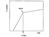
- It is a figure which shows the film-forming sequence which concerns on the 1st Embodiment of this invention. The state of the adsorption rate of TiCl 4 before and after the introduction of HCl is shown. It is a figure for demonstrating the 2nd Embodiment of this invention. It is a figure which shows the film-forming sequence which concerns on the 3rd Embodiment of this invention. It is a figure which shows the film-forming sequence which concerns on the 4th Embodiment of this invention.
- the substrate processing apparatus is configured as an example of a semiconductor manufacturing apparatus used for manufacturing a semiconductor device (IC Integrated Circuits).
- IC Integrated Circuits Integrated Circuits
- the substrate processing apparatus a case will be described in which a vertical apparatus that performs a film forming process or the like on a substrate is used.
- the present invention is not based on the use of a vertical apparatus, and for example, a single wafer apparatus may be used.
- the substrate processing apparatus 1 uses a cassette 100 that stores a wafer 200 as an example of a substrate, and the wafer 200 is made of a material such as silicon.
- the substrate processing apparatus 1 includes a housing 101, and a cassette stage 105 is installed inside the housing 101.
- the cassette 100 is carried on the cassette stage 105 by an in-process transfer device (not shown) or unloaded from the cassette stage 105.
- the cassette stage 105 is placed by the in-process transfer apparatus so that the wafer 200 in the cassette 100 maintains a vertical posture and the wafer loading / unloading port of the cassette 100 faces upward.
- the cassette stage 105 rotates the cassette 100 clockwise 90 ° to the rear of the casing 101 so that the wafer 200 in the cassette 100 is in a horizontal posture, and the wafer loading / unloading port of the cassette 100 faces the rear of the casing 101. It is configured to be operable.
- a cassette shelf 109 is installed at a substantially central portion in the front-rear direction in the housing 101, and the cassette shelf 109 is configured to store a plurality of cassettes 100 in a plurality of rows and a plurality of rows.
- the cassette shelf 109 is provided with a transfer shelf 123 in which the cassette 100 to be transferred by the wafer transfer mechanism 125 is stored.
- a reserve cassette shelf 110 is provided above the cassette stage 105, and is configured to store the cassette 100 preliminarily.
- a cassette transfer device 115 is installed between the cassette stage 105 and the cassette shelf 109.
- the cassette carrying device 115 includes a cassette elevator 115a that can move up and down while holding the cassette 100, and a cassette carrying mechanism 115b as a carrying mechanism.
- the cassette transport device 115 is configured to transport the cassette 100 among the cassette stage 105, the cassette shelf 109, and the spare cassette shelf 110 by continuous operation of the cassette elevator 115a and the cassette transport mechanism 115b.
- a wafer transfer mechanism 125 is installed behind the cassette shelf 109.
- the wafer transfer mechanism 125 includes a wafer transfer device 125a that can rotate or linearly move the wafer 200 in the horizontal direction, and a wafer transfer device elevator 125b that moves the wafer transfer device 125a up and down.
- the wafer transfer device 125 a is provided with a tweezer 125 c for picking up the wafer 200.
- the wafer transfer mechanism 125 loads (charges) the wafer 200 to the boat 217 by using the tweezers 125c as a placement portion of the wafer 200 by continuous operation of the wafer transfer device 125a and the wafer transfer device elevator 125b.
- the boat 217 is configured to be detached (discharged).
- a processing furnace 202 for heat-treating the wafer 200 is provided above the rear portion of the housing 101, and a lower end portion of the processing furnace 202 is configured to be opened and closed by a furnace port shutter 116.
- a boat elevator 121 that raises and lowers the boat 217 with respect to the processing furnace 202 is provided below the processing furnace 202.
- An arm 122 is connected to the lifting platform of the boat elevator 121, and a seal cap 219 is horizontally installed on the arm 122.
- the seal cap 219 is configured to support the boat 217 vertically and to close the lower end portion of the processing furnace 202.
- the boat 217 includes a plurality of holding members, and is configured to hold a plurality of (for example, about 50 to 150) wafers 200 horizontally with the centers thereof aligned in the vertical direction. Yes.
- the clean unit 134a for supplying clean air, which is a cleaned atmosphere, is installed.
- the clean unit 134 a includes a supply fan and a dustproof filter, and is configured to distribute clean air inside the housing 101.
- a clean unit 134 b for supplying clean air is installed at the left end of the housing 101.
- the clean unit 134b also includes a supply fan and a dustproof filter, and is configured to distribute clean air in the vicinity of the wafer transfer device 125a, the boat 217, and the like.
- the clean air is exhausted to the outside of the housing 101 after circulating in the vicinity of the wafer transfer device 125a, the boat 217, and the like.
- the cassette 100 When the cassette 100 is loaded onto the cassette stage 105 by an in-process transfer device (not shown), the cassette 100 holds the wafer 200 in a vertical position on the cassette stage 105 and the wafer loading / unloading port of the cassette 100 is directed upward. It is placed so that it faces. Thereafter, the cassette 100 is placed in a clockwise direction 90 in the clockwise direction behind the housing 101 so that the wafer 200 in the cassette 100 is placed in a horizontal posture by the cassette stage 105 and the wafer loading / unloading port of the cassette 100 faces the rear of the housing 101. ° Rotated.
- the cassette 100 is automatically transported and delivered to the designated shelf position of the cassette shelf 109 through the spare cassette shelf 110 by the cassette transport device 115, temporarily stored, and then stored in the cassette shelf 100 through the spare cassette shelf. It is transferred from 110 to the transfer shelf 123 by the cassette transfer device 115 or directly transferred to the transfer shelf 123.
- the wafer 200 is picked up from the cassette 100 through the wafer loading / unloading port by the tweezer 125c of the wafer transfer device 125a and loaded (charged) into the boat 217.
- the wafer transfer device 125 a that has delivered the wafer 200 to the boat 217 returns to the cassette 100 and loads the subsequent wafer 200 into the boat 217.
- the furnace port shutter 116 that has closed the lower end of the processing furnace 202 is opened, and the lower end of the processing furnace 202 is opened. Thereafter, the boat 217 holding the wafer group 200 is loaded into the processing furnace 202 by the ascending operation of the boat elevator 121, and the lower portion of the processing furnace 202 is closed by the seal cap 219.
- the processing furnace 202 is provided with a heater 207 which is a heating device (heating means) for heating the wafer 200.
- the heater 207 includes a cylindrical heat insulating member whose upper portion is closed and a plurality of heater wires, and has a unit configuration in which the heater wires are provided on the heat insulating member.
- a quartz reaction tube 203 for processing the wafer 200 is provided inside the heater 207.
- a manifold 209 made of stainless steel or the like is provided via an O-ring 220 that is an airtight member.
- the lower end opening of the manifold 209 is airtightly closed by a seal cap 219 as a lid through an O-ring 220.
- a processing chamber 201 is formed by at least the reaction tube 203, the manifold 209, and the seal cap 219.
- the seal cap 219 is provided with a boat support 218 that supports the boat 217.
- the boat 217 includes a bottom plate 210 fixed to the boat support base 218 and a top plate 211 disposed above the bottom plate 210, and a plurality of support columns are disposed between the bottom plate 210 and the top plate 211.
- 221 has a construction in which it is installed.
- a plurality of wafers 200 are held on the boat 217.
- the plurality of wafers 200 are supported by the column 221 of the boat 217 in a state where the wafer 200 is maintained in a horizontal posture while being spaced apart from each other.
- the boat 217 in a state where a plurality of batch-processed wafers 200 are stacked on the boat 217, the boat 217 is inserted into the processing chamber 201 while being supported by the boat support 218, and the heater 207 is The wafer 200 inserted into the processing chamber 201 is heated to a predetermined temperature.
- two gas supply pipes 310 and 320 (first gas supply pipe 310 and second gas supply pipe 320) for supplying source gas are connected to the processing chamber 201. Has been.
- the gas supply pipe 310 is provided with a mass flow controller 312 that is a flow rate control device (flow rate control means), a vaporizer 700 that is a vaporization unit (vaporization means), and a valve 314 that is an on-off valve in order from the upstream side.
- a nozzle 410 (first nozzle 410) is connected to the tip of the gas supply pipe 310.
- the first nozzle 410 is an arc-shaped space between the inner wall of the reaction tube 203 constituting the processing chamber 201 and the wafer 200, and the vertical direction along the inner wall of the reaction tube 203 (the loading direction of the wafer 200). It extends to.
- On the side surface of the first nozzle 410 a large number of gas supply holes 410a for supplying a source gas are provided.
- the gas supply holes 410a have the same or inclined opening areas from the lower part to the upper part, and are provided at the same opening pitch.
- the gas supply pipe 310 is provided with a vent line 610 and a valve 614 connected to an exhaust pipe 231 described later between the vaporizer 700 and the valve 314, and the source gas is not supplied to the processing chamber 201. Supplies the source gas to the vent line 610 via the valve 614.
- a gas supply pipe 310, a mass flow controller 312, a vaporizer 700, a valve 314, a first nozzle 410, a vent line 610, and a valve 614 constitute a first gas supply system (first source gas supply system).
- a carrier gas supply pipe 510 for supplying a carrier gas is connected to the gas supply pipe 310.
- the carrier gas supply pipe 510 is provided with a mass flow controller 512 and a valve 514.
- the carrier gas supply pipe 510, the mass flow controller 512, and the valve 514 mainly constitute a first carrier gas supply system (first inert gas supply system).
- the gas supply pipe 320 is provided with a mass flow controller 322 and a valve 324 which are flow rate control devices (flow rate control means) in order from the upstream side.
- a nozzle 420 (second nozzle 420) is connected to the distal end portion of the gas supply pipe 320.
- the second nozzle 420 is an arc-shaped space between the inner wall of the reaction tube 203 constituting the processing chamber 201 and the wafer 200, along the inner wall of the reaction tube 203. It extends in the vertical direction (the loading direction of the wafer 200).
- the gas supply holes 420a have the same or inclined opening areas from the lower part to the upper part, and are provided at the same opening pitch.
- the gas supply pipe 320, the mass flow controller 322, the valve 324, and the second nozzle 420 mainly constitute a second gas supply system (reformed gas supply system, reaction gas supply system).
- a carrier gas supply pipe 520 for supplying a carrier gas is connected to the gas supply pipe 320.
- the carrier gas supply pipe 520 is provided with a mass flow controller 522 and a valve 524.
- the carrier gas supply pipe 520, the mass flow controller 522, and the valve 524 mainly constitute a second carrier gas supply system (second inert gas supply system).
- a gas supply pipe 710 is connected to the gas supply pipe 310 on the downstream side of the junction between the gas supply pipe 310 and the carrier gas supply pipe 510.
- the gas supply pipe 710 is provided with a mass flow controller 712 and a valve 714.
- the gas supply pipe 710, the mass flow controller 712, and the valve 714 mainly constitute a third gas supply system (first Cl-containing gas supply system).
- a gas supply pipe 720 is connected to the gas supply pipe 320 on the downstream side of the junction of the gas supply pipe 320 and the carrier gas supply pipe 520.
- the gas supply pipe 720 is provided with a mass flow controller 722 and a valve 724.
- a gas supply pipe 720, a mass flow controller 722, and a valve 724 mainly constitute a fourth gas supply system (second Cl-containing gas supply system). In some cases, the fourth gas supply system may not be provided.
- the gas supply pipe 310 merges with the carrier gas supply pipe 510 via the mass flow controller 312, the vaporizer 700, and the valve 314, and further the gas supply pipe 710. Then, the reaction gas is supplied into the processing chamber 201 through the first nozzle 410.
- the mass flow controller 312 is replaced with a gas mass flow controller, and the vaporizer 700 becomes unnecessary.
- the gas supply pipe 320 merges with the carrier gas supply pipe 520 via the mass flow controller 322 and the valve 324, and further merges with the gas supply pipe 720, and then enters the processing chamber 201 via the second nozzle 420. Is supplied.
- the gas supply pipe 310 includes, for example, a titanium (Ti) -containing raw material (titanium tetrachloride (TiCl 4 ) or tetrakisdimethylaminotitanium (TDMAT), which is a metal raw material, as the first raw material gas.
- Ti titanium tetrachloride
- TDMAT tetrakisdimethylaminotitanium
- the gas supply pipe 320 includes an O-containing gas or an N-containing gas such as ammonia (NH 3 ), nitrogen (N 2 ), nitrogen, or the like, which is an O-containing gas or an N-containing gas as a reformed gas for reforming the raw material gas that is the first raw material.
- Nitrogen oxide (N 2 O), monomethylhydrazine (CH 6 N 2 ) or the like is introduced.
- hydrogen chloride (HCl), chlorine (Cl 2 ) or the like which is a Cl-containing gas, is introduced into the gas supply pipes 710 and 720 as a reaction gas to be reacted with the first raw material.
- the reaction tube 203 is provided with an exhaust pipe 231 for exhausting the atmosphere in the processing chamber 201.
- the exhaust pipe 231 is evacuated through a pressure detector (a pressure sensor 245 as a pressure detector and an APC (Auto Pressure Controller) valve 243 as a pressure regulator) for detecting the pressure in the processing chamber 201.
- a vacuum pump 246 as an apparatus (exhaust means) is connected, and is configured to be evacuated so that the pressure in the processing chamber 201 becomes a predetermined pressure (degree of vacuum).
- a temperature sensor 263 as a temperature detector is installed in the reaction tube 203, and the temperature in the processing chamber 201 is adjusted by adjusting the power supply to the heater 207 based on the temperature information detected by the temperature sensor 263. It is configured to have a desired temperature distribution.
- the temperature sensor 263 is configured in an L shape similarly to the nozzles 410 and 420, and is provided along the inner wall of the reaction tube 203.
- a boat 217 is provided in the center of the reaction tube 203.
- a boat rotation mechanism 267 that rotates the boat 217 is provided at the lower end of the boat support 218 that supports the boat 217 in order to improve processing uniformity.
- a rotation shaft 255 of the rotation mechanism 267 passes through the seal cap 219 and is connected to the boat 217, and is configured to rotate the wafer 200 by rotating the boat 217.
- the seal cap 219 is configured to be moved up and down in the vertical direction by a boat elevator 121 provided outside the reaction tube 203, so that the boat 217 can be carried into and out of the processing chamber 201. Yes.
- the controller 280 is an example of a control unit (control means) that controls the overall operation of the substrate processing apparatus 1.
- the controller 280 adjusts the flow rate of the mass flow controllers 312, 322, 512, 522, 712, 722, valves 314, 324, 514.
- TiCl 4 is used as a raw material gas containing titanium (Ti)
- NH 3 is used as a nitriding raw material that is a reformed gas
- HCl is used as a Cl-containing gas that is a reactive gas.
- FIG. 4 shows a film forming sequence of the titanium nitride film according to this embodiment.
- the controller 280 controls the substrate processing apparatus 1 as follows.
- the heater 207 is controlled to set the inside of the processing chamber 201 to a temperature in the range of 200 ° C. to 650 ° C., for example, and preferably 300 ° C. to 500 ° C.
- a plurality of wafers 200 are loaded into the boat 217, and the boat 217 is loaded into the processing chamber 201.
- the boat 217 is rotated by the boat driving mechanism 267 to rotate the wafer 200.
- the vacuum pump 246 is operated and the valve 243 is opened to evacuate the inside of the processing chamber 201.
- the temperature of the wafer 200 is, for example, in the range of 200 ° C. to 650 ° C., preferably 300 ° C. to 500 ° C.
- the sequence described later is performed in the state held in the above.
- Step 11 TiCl 4 is flowed.
- TiCl 4 is a liquid at room temperature, and is supplied to the processing chamber 201 by heating and vaporizing and supplying, He (helium), Ne (neon), called carrier gas using the vaporizer 700,
- He helium
- Ne neon
- carrier gas a gas such as He (helium), Ne (neon), called carrier gas using the vaporizer 700.
- an inert gas such as Ar (argon) or N 2 (nitrogen) is passed through a TiCl 4 container and the vaporized portion is supplied to the processing chamber 201 together with the carrier gas. The case will be described.
- TiCl 4 is passed through the gas supply pipe 310 and carrier gas (N 2 ) is passed through the carrier gas supply pipe 510.
- carrier gas N 2
- the valve 314 of the gas supply pipe 310, the valve 514 of the carrier gas supply pipe 510, and the APC valve 243 of the exhaust pipe 231 are all opened.
- the carrier gas flows from the carrier gas supply pipe 510 and the flow rate is adjusted by the mass flow controller 512.
- TiCl 4 flows from the gas supply pipe 310, the flow rate of which is adjusted by the mass flow controller 312, the vaporized gas of the vaporizer 700, and the carrier gas of which the flow rate is adjusted are mixed and supplied into the processing chamber 201 from the gas supply hole 410 a of the nozzle 410.
- the exhaust pipe 231 is exhausted while being exhausted.
- the APC valve 243 is appropriately adjusted to maintain the pressure in the processing chamber 201 within a range of 20 to 100 Pa, for example, 30 Pa.
- the supply amount of TiCl 4 controlled by the mass flow controller 312 is 1.0 to 2.0 g / min.
- the time for exposing the wafer 200 to TiCl 4 is 3 to 10 seconds.
- the temperature of the heater 207 is set so that the wafer temperature is in the range of 200 ° C. to 650 ° C., preferably 300 ° C. to 500 ° C., for example, 380 ° C.
- the gases flowing into the processing chamber 201 are only inert gases such as TiCl 4 , N 2 , and Ar, and NH 3 and HCl do not exist. Therefore, TiCl 4 does not cause a gas phase reaction, and reacts with the surface of the wafer 200 and the underlying film (chemical adsorption) to form an adsorption layer or a Ti layer (hereinafter referred to as a Ti-containing layer) of the raw material (TiCl 4 ).
- the adsorption layer of TiCl 4 includes a continuous adsorption layer of raw material molecules and a discontinuous adsorption layer.
- the Ti layer includes not only a continuous layer composed of Ti but also a Ti thin film formed by overlapping these layers.
- the continuous layer comprised by Ti may be called Ti thin film.
- the inert gas is flowed from the carrier gas supply pipe 520 connected to the middle of the gas supply pipe 320 by opening the valve 524.
- TiCl 4 can be prevented from entering the NH 3 side.
- Step 12 HCl is flowed. HCl serves to suppress the growth of TiN. HCl is passed through the gas supply pipe 710. The valve 714 of the gas supply pipe 710 is opened. The TiCl 4 that has been mixed and supplied from the gas supply pipe 310 with the carrier gas is mixed with HCl whose flow rate has been adjusted by the mass flow controller 712, and is supplied into the processing chamber 201 from the gas supply hole 410a of the nozzle 410 while being exhausted. 231 is exhausted.
- an inert gas such as N 2 is continuously supplied into the processing chamber 201 from the gas supply hole 420 a of the nozzle 420.
- Step 13 The valve 314 of the gas supply pipe 310 is closed to stop the supply of TiCl 4 to the processing chamber, and the valve 614 is opened to flow TiCl 4 to the vent line 610. Accordingly, only HCl mixed with the carrier gas is supplied from the gas supply hole 410a of the nozzle 410.
- the APC valve 243 is appropriately adjusted to maintain the pressure in the processing chamber 201 within a range of 10 to 50 Pa, for example, 20 Pa.
- the supply flow rate of HCl controlled by the mass flow controller 712 is 0.5 to 5 slm.
- the time for exposing the wafer 200 to HCl is 1 to 5 seconds.
- the temperature of the heater 207 at this time is set so that the wafer temperature is in the range of 200 ° C. to 650 ° C., preferably 300 ° C. to 500 ° C., for example, 380 ° C.
- Step 14 The valve 714 of the gas supply pipe 710 is closed, and supply of HCl into the processing chamber 201 is stopped. At this time, the APC valve 243 of the gas exhaust pipe 231 is kept open, and the inside of the processing chamber 201 is exhausted to 10 Pa or less by the vacuum pump 246 to remove the residual TiCl 4 from the processing chamber 201. At this time, an inert gas such as N 2 is continuously supplied into the processing chamber 201 from the gas supply hole 420 a of the nozzle 420. This further increases the effect of eliminating residual TiCl 4 .
- Step 15 NH 3 is flowed.
- NH 3 flows through the gas supply pipe 320 and carrier gas (N 2 ) flows through the carrier gas supply pipe 520.
- the valve 324 of the gas supply pipe 320, the valve 522 of the carrier gas supply pipe 520, and the APC valve 243 of the exhaust pipe 231 are all opened.
- the carrier gas flows from the carrier gas supply pipe 520 and the flow rate is adjusted by the mass flow controller 522.
- NH 3 flows from the gas supply pipe 320, is adjusted in flow rate by the mass flow controller 322, mixes the adjusted carrier gas, and is exhausted from the exhaust pipe 231 while being supplied from the gas supply hole 420 a of the nozzle 420 into the processing chamber 201. Is done.
- the APC valve 243 When flowing NH 3 , the APC valve 243 is appropriately adjusted to maintain the pressure in the processing chamber 201 within a range of 50 to 1000 Pa, for example, 60 Pa.
- the supply flow rate of NH 3 controlled by the mass flow controller 324 is 1 to 10 slm.
- the time for exposing the wafer 200 to NH 3 is 10 to 45 seconds.
- the temperature of the heater 207 at this time is set so that the wafer temperature is in the range of 200 ° C. to 650 ° C., preferably 300 ° C. to 500 ° C., for example, 380 ° C.
- the Ti-containing layer chemically adsorbed on the wafer 200 and NH 3 undergo a surface reaction (chemical adsorption), and a titanium nitride film is formed on the wafer 200.
- Step 16 the APC valve 324 of the gas supply pipe 320 is closed to stop the supply of NH 3 . Further, the APC valve 243 of the gas exhaust pipe 231 is kept open, the processing chamber 201 is exhausted to 10 Pa or less by the vacuum pump 246, and residual NH 3 is removed from the processing chamber 201. At this time, if inert gas such as N 2 is supplied to the processing chamber 201 from the gas supply pipe 320 that is an NH 3 supply line and the gas supply pipe 310 that is a TiCl 4 supply line and is purged, residual NH 3 The effect of eliminating is further enhanced.
- inert gas such as N 2
- the above steps 11 to 16 are defined as one cycle, and a titanium nitride film having a predetermined thickness is formed on the wafer 200 by performing at least once.
- TiCl 4 As described above, by introducing TiCl 4 into the processing chamber 201, TiCl 4 is adsorbed on the adsorption sites on the wafer 200, and the surface of the wafer 200 is gradually covered with TiClx.
- the required time varies depending on the environmental temperature, the introduction flow rate, the pressure, etc., but is approximately several seconds to several tens of seconds.
- HCl that is a reaction suppressing substance is introduced in a state where TiCl 4 is introduced at a timing (before saturation) before TiCl 4 is adsorbed on all adsorption sites.
- the introduced HCl fills a part of the adsorption site, and the adsorption of TiCl 4 is inhibited.
- NH 3 is introduced. This NH 3 reacts with TiClx on the surface of the substrate to be processed to grow TiN and at the same time has a function of desorbing HCl from the surface. Further, after removing excess NH 3 in the processing chamber 201, a high-quality TiN film can be obtained by repeating the above processing until a desired film thickness is obtained.
- the amount of Ti adsorbed on the substrate is reduced by supplying HCl as a reaction inhibitor, and then NH 3 is supplied to react with a sufficient amount of nitrogen. As a result, a more nitrogen-rich film is formed, and the resistivity of the film is considered to be low.
- the reaction-inhibiting substance is introduced into the processing chamber 201 to realize the continuous film formation of less than one atomic layer.
- the reaction-inhibiting substance is not introduced, and the reaction gas and the reaction conditions are optimized.
- the by-product is used for reaction suppression.
- the amount of film formation at the inflection point can be controlled by controlling the film formation temperature or pressure.
- TiCl 4 is used as a raw material gas containing titanium (Ti) and NH 3 is used as a nitriding raw material that is a reformed gas.
- the controller 280 controls the substrate processing apparatus 1 as follows, as in the first embodiment. That is, by controlling the heater 207, the inside of the processing chamber 201 is set to a temperature in the range of 250 ° C. to 450 ° C., and the pressure in the processing chamber 201 is maintained at 10 Pa to 100 Pa.
- FIG. 6 shows an example in which a TiN film is formed using the above-described conditions. As shown in FIG. 6, the amount of film formation per time obtained by dividing the final film thickness by the number of times of sequential film formation using the introduction time of TiCl 4 per time of sequential film formation as a parameter is 1 atom.
- the atomic layer of TiN crystal in the low-order plane orientation is about 1 to 3 mm, and in this example, about 1/10 to 1/4 atomic layer was formed per one sequential film formation. I understand.
- FIG. 7 shows a film forming sequence of the titanium nitride film according to the third embodiment. In the third embodiment, only portions different from the first embodiment will be described.
- Step 21 TiCl 4 is supplied to the processing chamber via the nozzle 410 under the same conditions as in step 11. At this time, an inert gas such as N 2 is supplied from the nozzle 420 to the processing chamber.
- Step 22 As in Step 12, with TiCl 4 supplied to the processing chamber, HCl is supplied from the gas supply pipe 710 to the processing chamber via the nozzle 410. At this time, an inert gas such as N 2 is continuously supplied from the nozzle 420 to the processing chamber.
- Step 23 As in step 13, with HCl supplied to the processing chamber, the valve 314 of the gas supply pipe 310 is closed to stop the supply of TiCl 4 to the processing chamber, and the valve 614 is opened to allow TiCl 4 to flow into the vent line 610.
- Step 24 As in step 14, the valve 714 of the gas supply pipe 710 is closed to stop the supply of HCl to the processing chamber. At this time, the APC valve 243 of the gas exhaust pipe 231 is kept open, and the inside of the processing chamber 201 is evacuated to 20 Pa or less by the vacuum pump 246 to remove residual TiCl 4 from the processing chamber 201. At this time, if an inert gas such as N 2 is supplied from the nozzle 420 into the processing chamber 201, the effect of removing residual TiCl 4 is further enhanced.
- an inert gas such as N 2
- Step 25 NH 3 is supplied to the processing chamber under the same conditions as in step 15. NH 3 flows through the gas supply pipe 320 and carrier gas (N 2 ) flows through the carrier gas supply pipe 520.
- Step 26 the valve 324 of the gas supply pipe 320 is closed to stop the supply of NH 3 . Further, the APC valve 243 of the gas exhaust pipe 231 is kept open, the processing chamber 201 is exhausted to 20 Pa or less by the vacuum pump 246, and residual NH 3 is removed from the processing chamber 201.
- Step 27 NH 3 is again supplied to the processing chamber and light or plasma is irradiated. NH 3 is allowed to flow under the same conditions as in step 15 and step 25, for example.
- Step 28 the valve 324 of the gas supply pipe 320 is closed to stop the supply of NH 3 . Further, the APC valve 243 of the gas exhaust pipe 231 is kept open, the processing chamber 201 is exhausted to 20 Pa or less by the vacuum pump 246, and residual NH 3 is removed from the processing chamber 201.
- Steps 21 to 28 are defined as one cycle, and a predetermined number of times is performed at least once to form a titanium nitride film having a predetermined thickness on the wafer 200.
- a predetermined number of times is performed at least once to form a titanium nitride film having a predetermined thickness on the wafer 200.
- FIG. 8 shows a film forming sequence of the titanium nitride film according to the fourth embodiment. In the fourth embodiment, only portions different from the first embodiment will be described.
- Step 31 TiCl 4 is supplied to the processing chamber under the same conditions as in step 11. At this time, the temperature of the heater 207 is set so that the wafer temperature is in the range of 200 ° C. to 550 ° C., preferably 350 ° C. to 450 ° C., for example, 380 ° C.
- Step 32 As in Step 12, with TiCl 4 supplied to the processing chamber, HCl is supplied from the gas supply pipe 710 to the processing chamber via the nozzle 410. At this time, an inert gas such as N 2 is continuously supplied from the nozzle 420 to the processing chamber.
- Step 33 As in step 13, with HCl supplied to the processing chamber, the valve 314 of the gas supply pipe 310 is closed to stop the supply of TiCl 4 to the processing chamber, and the valve 614 is opened to allow TiCl 4 to flow into the vent line 610.
- Step 34 As in step 14, the valve 714 of the gas supply pipe 710 is closed to stop the supply of HCl to the processing chamber. At this time, the APC valve 243 of the gas exhaust pipe 231 is kept open, and the inside of the processing chamber 201 is evacuated to 10 Pa or less by the vacuum pump 246 to remove residual TiCl 4 from the processing chamber 201. At this time, if an inert gas such as N 2 is supplied into the processing chamber 201, the effect of removing residual TiCl 4 is further enhanced.
- an inert gas such as N 2
- Step 35 NH 3 is supplied under the same conditions as in step 15. NH 3 flows through the gas supply pipe 320 and carrier gas (N 2 ) flows through the carrier gas supply pipe 520.
- Step 36 the valve 324 of the gas supply pipe 320 is closed to stop the supply of NH 3 . Further, the APC valve 243 of the gas exhaust pipe 231 is kept open, the processing chamber 201 is exhausted to 20 Pa or less by the vacuum pump 246, and residual NH 3 is removed from the processing chamber 201.
- step 37 temperature increase in the processing chamber is started.
- Step 38 In step 38, NH 3 is supplied again. NH 3 is allowed to flow under the same conditions as in steps 15 and 25. At this time, the temperature of the heater 207 is set so that the wafer temperature is in the range of 300 ° C. to 650 ° C., preferably 400 ° C. to 650 ° C., for example, 650 ° C.
- Step 39 In step 39, the valve 324 of the gas supply pipe 320 is closed, the supply of NH 3 is stopped, and the temperature in the processing chamber is lowered.
- Step 40 The temperature in the treatment chamber is in the range of 200 ° C. to 550 ° C., preferably 350 ° C. to 450 ° C.
- the APC valve 243 of the gas exhaust pipe 231 is kept open, the processing chamber 201 is exhausted to 10 Pa or less by the vacuum pump 246, and residual NH 3 is removed from the processing chamber 201.
- the above steps 31 to 40 are defined as one cycle, and a titanium nitride film having a predetermined thickness is formed on the wafer 200 by performing at least once and a predetermined number of times.
- a titanium nitride film having a predetermined thickness is formed on the wafer 200 by performing at least once and a predetermined number of times.
- separation of the reaction inhibitor is promoted, and NH 3 is introduced so that nitriding proceeds even when unreacted Ti is scattered.
- the temperature increase and the NH 3 introduction are performed at the same time.
- HCl which is a reaction inhibitor
- HCl is not supplied from outside the processing chamber, and reaction by-products are generated in the processing chamber. This process is effective even when HCl generated as a product is supplied to the surface of the wafer 200.
- reaction-suppressing substance may be supplied from all nozzles (for example, nozzle 410 and nozzle 420).
- the present invention it is possible to suppress the residue of impurities in the film by performing the further sequential film formation as compared with the ALD method. Furthermore, since the surface layer of the thin film that is the target for modification can be made thinner, more effective film quality improvement can be performed.
- a portion where growth of less than one atomic layer has occurred is described as a thin film or layer for the sake of convenience, and the growth of less than one atomic layer here is a thin film having an originally assumed plane orientation.
- the number of atoms per unit area contained in a thin film grown by one sequential film formation is smaller than the number of atoms per unit area for constituting one atomic layer.
- the vertical apparatus has been mainly described.
- the formation of the titanium nitride film using at least two or more different CVD methods in the present invention is not limited to the vertical apparatus, but other devices such as a single wafer apparatus. It is also applicable to the device.
- the vertical thermal CVD apparatus has been mainly described.
- the formation of the titanium nitride film using at least two or more different CVD methods in the present invention is not limited to the thermal CVD apparatus, but a plasma CVD apparatus.
- the present invention can also be applied to other apparatuses such as a photo-CVD apparatus.
- titanium nitride film is formed on a substrate by reacting titanium tetrachloride (TiCl 4 ) with ammonia (NH 3 )
- TiCl 4 titanium tetrachloride
- NH 3 ammonia
- the present invention is not limited to this, and other film types are used. Is also applicable.
- the present invention is applicable to nitrides such as titanium nitride (TiN) and tantalum nitride (TaN) and metal compounds to which elements are mainly added.
- the method of manufacturing a semiconductor device that forms a film of less than one atomic layer on the surface of the substrate is provided.
- the reaction gas is a Cl-containing gas.
- the first raw material is a metal raw material
- the reformed gas is an O-containing gas or an N-containing gas.
- the reformed gas is activated by using heat, light, or plasma.
- the temperature of the substrate is set to 200 to 550 ° C.
- the temperature of the substrate is set to 300 to 450 ° C.
- the temperature of the substrate is set to be equal to or lower than the self-decomposition temperature of the first raw material.
- the first raw material is supplied to the processing chamber in which the substrate is accommodated to adsorb the first raw material less than one atomic layer on the surface of the substrate. And a second step of supplying a reforming gas for reforming the first raw material adsorbed on the surface of the substrate to the processing chamber, thereby forming a single atomic layer on the surface of the substrate.
- a third step of removing the atmosphere in the processing chamber, and a reforming gas for reforming the first raw material is supplied to the processing chamber to reform the first raw material adsorbed on the substrate.
- a fourth step of removing the atmosphere in the processing chamber; a reforming gas supplied to the processing chamber while activating the reformed gas; and reforming the first raw material adsorbed on the substrate A semiconductor device that forms a film of less than one atomic layer on the surface of the substrate by sequentially performing the sixth step Manufacturing method is provided. (Appendix 10) According to another aspect of the present invention, the first raw material is supplied to the surface of the substrate while supplying the first raw material to the processing chamber in which the substrate is accommodated at the first temperature.
- Appendix 11 Preferably, a film having less than one atomic layer is formed on the surface of the substrate by providing an inflection point in the growth rate of the film.
- Appendix 12 a semiconductor device manufactured using any one of the manufacturing methods of the semiconductor device described in Appendix 1 to Appendix 11 is provided.
- a processing chamber that accommodates a substrate, a source gas supply system that supplies a source gas containing a first element to the processing chamber, and the first element in the processing chamber
- a reaction gas supply system that supplies a reaction gas that reacts with the gas
- a Cl-containing gas supply system that supplies a Cl-containing gas to the processing chamber
- an exhaust system that exhausts the processing chamber, the source gas supply system, and the reaction gas
- a control unit that controls a supply system, the Cl-containing gas supply system, and the exhaust system, wherein the control unit includes the source gas supply system, the reaction gas supply system, the Cl-containing gas supply system, and the exhaust gas.
- the system is controlled to supply the first source gas to adsorb at least the first element on the surface of the substrate, and the reactive gas before the first source is saturated and adsorbed on the surface of the substrate.
- a substrate processing apparatus is provided for forming a film of less than one atomic layer on the surface of the substrate.
- Substrate processing apparatus 200 Wafer 201 Processing chamber 202 Processing furnace 203 Reaction tube 207 Heater 217 Boat 218 Boat support 231 Exhaust pipe 243 APC valve 246 Vacuum pump 267 Boat rotation mechanism 280 Controller 410, 420 Nozzle 410a, 420a Gas supply hole
Landscapes
- Chemical & Material Sciences (AREA)
- Engineering & Computer Science (AREA)
- Mechanical Engineering (AREA)
- Chemical Kinetics & Catalysis (AREA)
- General Chemical & Material Sciences (AREA)
- Materials Engineering (AREA)
- Metallurgy (AREA)
- Organic Chemistry (AREA)
- Inorganic Chemistry (AREA)
- Chemical Vapour Deposition (AREA)
- Physics & Mathematics (AREA)
- Plasma & Fusion (AREA)
- Electrodes Of Semiconductors (AREA)
Priority Applications (3)
| Application Number | Priority Date | Filing Date | Title |
|---|---|---|---|
| US13/693,647 US20130095668A1 (en) | 2010-06-04 | 2012-12-04 | Semiconductor device manufacturing method and substrate processing apparatus |
| US14/680,841 US9340873B2 (en) | 2010-06-04 | 2015-04-07 | Semiconductor device manufacturing method and substrate processing apparatus |
| US14/874,967 US9416446B2 (en) | 2010-06-04 | 2015-10-05 | Semiconductor device manufacturing method and substrate processing apparatus |
Applications Claiming Priority (2)
| Application Number | Priority Date | Filing Date | Title |
|---|---|---|---|
| JP2010128417A JP5692842B2 (ja) | 2010-06-04 | 2010-06-04 | 半導体装置の製造方法及び基板処理装置 |
| JP2010-128417 | 2010-06-04 |
Related Child Applications (1)
| Application Number | Title | Priority Date | Filing Date |
|---|---|---|---|
| US13/693,647 Continuation US20130095668A1 (en) | 2010-06-04 | 2012-12-04 | Semiconductor device manufacturing method and substrate processing apparatus |
Publications (1)
| Publication Number | Publication Date |
|---|---|
| WO2011152352A1 true WO2011152352A1 (ja) | 2011-12-08 |
Family
ID=45066719
Family Applications (1)
| Application Number | Title | Priority Date | Filing Date |
|---|---|---|---|
| PCT/JP2011/062381 Ceased WO2011152352A1 (ja) | 2010-06-04 | 2011-05-30 | 半導体装置の製造方法及び基板処理装置 |
Country Status (3)
| Country | Link |
|---|---|
| US (3) | US20130095668A1 (https=) |
| JP (1) | JP5692842B2 (https=) |
| WO (1) | WO2011152352A1 (https=) |
Families Citing this family (19)
| Publication number | Priority date | Publication date | Assignee | Title |
|---|---|---|---|---|
| JP6164775B2 (ja) * | 2014-08-21 | 2017-07-19 | 株式会社日立国際電気 | 半導体デバイスの製造方法、基板処理装置およびプログラム |
| JP6436887B2 (ja) * | 2015-09-30 | 2018-12-12 | 株式会社Kokusai Electric | 半導体装置の製造方法、基板処理装置、ガス供給システムおよびプログラム |
| KR102466140B1 (ko) * | 2016-01-29 | 2022-11-11 | 삼성전자주식회사 | 가열 장치 및 이를 갖는 기판 처리 시스템 |
| KR102474303B1 (ko) * | 2016-02-02 | 2022-12-06 | 에스케이하이닉스 주식회사 | 스위칭 소자, 저항 변화 메모리 장치, 스위칭 소자의 제조 방법, 및 저항 변화 메모리 장치의 제조 방법 |
| US10468264B2 (en) * | 2016-07-04 | 2019-11-05 | Samsung Electronics Co., Ltd. | Method of fabricating semiconductor device |
| KR102375981B1 (ko) * | 2016-07-04 | 2022-03-18 | 삼성전자주식회사 | 반도체 장치 제조 방법 및 반도체 장치 제조 설비 |
| JP6602332B2 (ja) * | 2017-03-28 | 2019-11-06 | 株式会社Kokusai Electric | 半導体装置の製造方法、基板処理装置およびプログラム |
| TWI709163B (zh) * | 2017-09-26 | 2020-11-01 | 日商國際電氣股份有限公司 | 基板處理裝置、半導體裝置之製造方法及程式 |
| TWI699907B (zh) * | 2018-01-25 | 2020-07-21 | 致伸科技股份有限公司 | 光源模組 |
| JP7113670B2 (ja) * | 2018-06-08 | 2022-08-05 | 東京エレクトロン株式会社 | Ald成膜方法およびald成膜装置 |
| KR102141547B1 (ko) * | 2019-09-25 | 2020-09-14 | 솔브레인 주식회사 | 박막 제조 방법 |
| JP6857760B2 (ja) * | 2020-02-18 | 2021-04-14 | 株式会社Kokusai Electric | 半導体装置の製造方法、基板処理装置、およびプログラム |
| JP7273079B2 (ja) | 2021-02-15 | 2023-05-12 | 株式会社Kokusai Electric | 基板処理装置、半導体装置の製造方法、プログラムおよび基板処理方法 |
| JP7248722B2 (ja) | 2021-02-19 | 2023-03-29 | 株式会社Kokusai Electric | 基板処理方法、基板処理装置、プログラムおよび半導体装置の製造方法 |
| CN113430501A (zh) * | 2021-06-18 | 2021-09-24 | 长江先进存储产业创新中心有限责任公司 | 薄膜沉积设备和薄膜沉积方法 |
| JP7575358B2 (ja) | 2021-08-05 | 2024-10-29 | 株式会社Kokusai Electric | 半導体装置の製造方法、基板処理装置、プログラム及び基板処理方法 |
| JP2023137871A (ja) | 2022-03-18 | 2023-09-29 | 株式会社Kokusai Electric | 基板処理方法、半導体装置の製造方法、プログラム及び基板処理装置 |
| JP2025131950A (ja) | 2022-08-09 | 2025-09-10 | 株式会社Kokusai Electric | 基板処理装置、基板支持具、基板処理方法及びプログラム |
| JP2025007482A (ja) * | 2023-06-30 | 2025-01-17 | 株式会社Kokusai Electric | 基板処理方法、半導体装置の製造方法、プログラム、基板処理装置 |
Citations (4)
| Publication number | Priority date | Publication date | Assignee | Title |
|---|---|---|---|---|
| JP2008199052A (ja) * | 2001-05-07 | 2008-08-28 | Samsung Electronics Co Ltd | 多成分系薄膜及びその形成方法 |
| JP2008277777A (ja) * | 2007-04-02 | 2008-11-13 | Hitachi Kokusai Electric Inc | 半導体装置の製造方法 |
| JP2009263764A (ja) * | 2008-04-01 | 2009-11-12 | Hitachi Kokusai Electric Inc | 半導体製造装置及び半導体装置の製造方法 |
| JP2011132589A (ja) * | 2009-12-25 | 2011-07-07 | Tokyo Electron Ltd | 成膜装置、成膜方法及び記憶媒体 |
Family Cites Families (14)
| Publication number | Priority date | Publication date | Assignee | Title |
|---|---|---|---|---|
| JPH07226380A (ja) | 1994-02-10 | 1995-08-22 | Nippon Telegr & Teleph Corp <Ntt> | 原子層結晶成長法 |
| EP1256638B1 (en) * | 2001-05-07 | 2008-03-26 | Samsung Electronics Co., Ltd. | Method of forming a multi-components thin film |
| JP4024624B2 (ja) * | 2002-08-26 | 2007-12-19 | 富士通株式会社 | 半導体装置の製造方法及び製造装置 |
| US6863725B2 (en) * | 2003-02-04 | 2005-03-08 | Micron Technology, Inc. | Method of forming a Ta2O5 comprising layer |
| US7981473B2 (en) * | 2003-04-23 | 2011-07-19 | Aixtron, Inc. | Transient enhanced atomic layer deposition |
| US7258895B2 (en) * | 2003-08-06 | 2007-08-21 | Micron Technology, Inc. | Methods of forming material on a substrate, and a method of forming a field effect transistor gate oxide on a substrate |
| US7572731B2 (en) * | 2005-06-28 | 2009-08-11 | Micron Technology, Inc. | Unsymmetrical ligand sources, reduced symmetry metal-containing compounds, and systems and methods including same |
| JP4727667B2 (ja) | 2005-08-16 | 2011-07-20 | 株式会社日立国際電気 | 薄膜形成方法および半導体デバイスの製造方法 |
| US8282733B2 (en) | 2007-04-02 | 2012-10-09 | Hitachi Kokusai Electric Inc. | Manufacturing method of semiconductor apparatus |
| EP2166562B1 (en) * | 2008-09-22 | 2019-03-20 | IMEC vzw | Method for forming a capacitor having a strontium titanium oxide dielectric layer by means of ALD |
| JP5384291B2 (ja) * | 2008-11-26 | 2014-01-08 | 株式会社日立国際電気 | 半導体装置の製造方法、基板処理方法及び基板処理装置 |
| ES2923774T3 (es) * | 2010-05-21 | 2022-09-30 | Asm Int Nv | Método de fabricación de una celda solar |
| US20140175367A1 (en) * | 2012-12-20 | 2014-06-26 | Intermolecular Inc. | Materials for Thin Resisive Switching Layers of Re-RAM Cells |
| US8852996B2 (en) * | 2012-12-20 | 2014-10-07 | Intermolecular, Inc. | Carbon doped resistive switching layers |
-
2010
- 2010-06-04 JP JP2010128417A patent/JP5692842B2/ja active Active
-
2011
- 2011-05-30 WO PCT/JP2011/062381 patent/WO2011152352A1/ja not_active Ceased
-
2012
- 2012-12-04 US US13/693,647 patent/US20130095668A1/en not_active Abandoned
-
2015
- 2015-04-07 US US14/680,841 patent/US9340873B2/en active Active
- 2015-10-05 US US14/874,967 patent/US9416446B2/en active Active
Patent Citations (4)
| Publication number | Priority date | Publication date | Assignee | Title |
|---|---|---|---|---|
| JP2008199052A (ja) * | 2001-05-07 | 2008-08-28 | Samsung Electronics Co Ltd | 多成分系薄膜及びその形成方法 |
| JP2008277777A (ja) * | 2007-04-02 | 2008-11-13 | Hitachi Kokusai Electric Inc | 半導体装置の製造方法 |
| JP2009263764A (ja) * | 2008-04-01 | 2009-11-12 | Hitachi Kokusai Electric Inc | 半導体製造装置及び半導体装置の製造方法 |
| JP2011132589A (ja) * | 2009-12-25 | 2011-07-07 | Tokyo Electron Ltd | 成膜装置、成膜方法及び記憶媒体 |
Also Published As
| Publication number | Publication date |
|---|---|
| JP5692842B2 (ja) | 2015-04-01 |
| US9340873B2 (en) | 2016-05-17 |
| US20160024649A1 (en) | 2016-01-28 |
| US9416446B2 (en) | 2016-08-16 |
| JP2011252221A (ja) | 2011-12-15 |
| US20130095668A1 (en) | 2013-04-18 |
| US20150214045A1 (en) | 2015-07-30 |
Similar Documents
| Publication | Publication Date | Title |
|---|---|---|
| JP5692842B2 (ja) | 半導体装置の製造方法及び基板処理装置 | |
| JP5774822B2 (ja) | 半導体デバイスの製造方法及び基板処理装置 | |
| JP5787488B2 (ja) | 半導体装置の製造方法及び基板処理装置 | |
| JP5963456B2 (ja) | 半導体装置の製造方法、基板処理装置、及び基板処理方法 | |
| US9238257B2 (en) | Method of manufacturing semiconductor device, cleaning method, and substrate processing apparatus | |
| JP5610438B2 (ja) | 基板処理装置及び半導体装置の製造方法 | |
| JP5087657B2 (ja) | 半導体装置の製造方法及び基板処理装置 | |
| TWI483313B (zh) | 半導體裝置之製造方法及基板處理裝置 | |
| JP5518499B2 (ja) | 半導体デバイスの製造方法および基板処理装置 | |
| KR101737215B1 (ko) | 반도체 장치의 제조 방법, 기판 처리 장치 및 프로그램 | |
| JP5718031B2 (ja) | 基板処理装置および半導体装置の製造方法 | |
| JP2012172171A (ja) | 基板処理装置及び薄膜成膜方法 | |
| JP5306691B2 (ja) | 半導体装置の製造方法、基板処理方法および基板処理装置 | |
| JP2012015344A (ja) | 半導体装置の製造方法 | |
| JP5421812B2 (ja) | 半導体基板の成膜装置及び方法 | |
| JP2011151294A (ja) | 半導体装置の製造方法 | |
| JP5557896B2 (ja) | 半導体装置の製造方法、基板処理方法および基板処理装置 | |
| JP2007049046A (ja) | 半導体装置の製造方法 | |
| JP2012233265A (ja) | 半導体装置の製造方法及び基板処理装置 |
Legal Events
| Date | Code | Title | Description |
|---|---|---|---|
| 121 | Ep: the epo has been informed by wipo that ep was designated in this application |
Ref document number: 11789755 Country of ref document: EP Kind code of ref document: A1 |
|
| NENP | Non-entry into the national phase |
Ref country code: DE |
|
| 122 | Ep: pct application non-entry in european phase |
Ref document number: 11789755 Country of ref document: EP Kind code of ref document: A1 |