WO2011152352A1 - Method for manufacturing semiconductor device and substrate processing apparatus - Google Patents
Method for manufacturing semiconductor device and substrate processing apparatus Download PDFInfo
- Publication number
- WO2011152352A1 WO2011152352A1 PCT/JP2011/062381 JP2011062381W WO2011152352A1 WO 2011152352 A1 WO2011152352 A1 WO 2011152352A1 JP 2011062381 W JP2011062381 W JP 2011062381W WO 2011152352 A1 WO2011152352 A1 WO 2011152352A1
- Authority
- WO
- WIPO (PCT)
- Prior art keywords
- substrate
- processing chamber
- raw material
- gas supply
- gas
- Prior art date
Links
Images


Classifications
-
- C—CHEMISTRY; METALLURGY
- C23—COATING METALLIC MATERIAL; COATING MATERIAL WITH METALLIC MATERIAL; CHEMICAL SURFACE TREATMENT; DIFFUSION TREATMENT OF METALLIC MATERIAL; COATING BY VACUUM EVAPORATION, BY SPUTTERING, BY ION IMPLANTATION OR BY CHEMICAL VAPOUR DEPOSITION, IN GENERAL; INHIBITING CORROSION OF METALLIC MATERIAL OR INCRUSTATION IN GENERAL
- C23C—COATING METALLIC MATERIAL; COATING MATERIAL WITH METALLIC MATERIAL; SURFACE TREATMENT OF METALLIC MATERIAL BY DIFFUSION INTO THE SURFACE, BY CHEMICAL CONVERSION OR SUBSTITUTION; COATING BY VACUUM EVAPORATION, BY SPUTTERING, BY ION IMPLANTATION OR BY CHEMICAL VAPOUR DEPOSITION, IN GENERAL
- C23C16/00—Chemical coating by decomposition of gaseous compounds, without leaving reaction products of surface material in the coating, i.e. chemical vapour deposition [CVD] processes
- C23C16/44—Chemical coating by decomposition of gaseous compounds, without leaving reaction products of surface material in the coating, i.e. chemical vapour deposition [CVD] processes characterised by the method of coating
- C23C16/4401—Means for minimising impurities, e.g. dust, moisture or residual gas, in the reaction chamber
- C23C16/4408—Means for minimising impurities, e.g. dust, moisture or residual gas, in the reaction chamber by purging residual gases from the reaction chamber or gas lines
-
- C—CHEMISTRY; METALLURGY
- C23—COATING METALLIC MATERIAL; COATING MATERIAL WITH METALLIC MATERIAL; CHEMICAL SURFACE TREATMENT; DIFFUSION TREATMENT OF METALLIC MATERIAL; COATING BY VACUUM EVAPORATION, BY SPUTTERING, BY ION IMPLANTATION OR BY CHEMICAL VAPOUR DEPOSITION, IN GENERAL; INHIBITING CORROSION OF METALLIC MATERIAL OR INCRUSTATION IN GENERAL
- C23C—COATING METALLIC MATERIAL; COATING MATERIAL WITH METALLIC MATERIAL; SURFACE TREATMENT OF METALLIC MATERIAL BY DIFFUSION INTO THE SURFACE, BY CHEMICAL CONVERSION OR SUBSTITUTION; COATING BY VACUUM EVAPORATION, BY SPUTTERING, BY ION IMPLANTATION OR BY CHEMICAL VAPOUR DEPOSITION, IN GENERAL
- C23C16/00—Chemical coating by decomposition of gaseous compounds, without leaving reaction products of surface material in the coating, i.e. chemical vapour deposition [CVD] processes
- C23C16/22—Chemical coating by decomposition of gaseous compounds, without leaving reaction products of surface material in the coating, i.e. chemical vapour deposition [CVD] processes characterised by the deposition of inorganic material, other than metallic material
- C23C16/30—Deposition of compounds, mixtures or solid solutions, e.g. borides, carbides, nitrides
- C23C16/34—Nitrides
-
- C—CHEMISTRY; METALLURGY
- C23—COATING METALLIC MATERIAL; COATING MATERIAL WITH METALLIC MATERIAL; CHEMICAL SURFACE TREATMENT; DIFFUSION TREATMENT OF METALLIC MATERIAL; COATING BY VACUUM EVAPORATION, BY SPUTTERING, BY ION IMPLANTATION OR BY CHEMICAL VAPOUR DEPOSITION, IN GENERAL; INHIBITING CORROSION OF METALLIC MATERIAL OR INCRUSTATION IN GENERAL
- C23C—COATING METALLIC MATERIAL; COATING MATERIAL WITH METALLIC MATERIAL; SURFACE TREATMENT OF METALLIC MATERIAL BY DIFFUSION INTO THE SURFACE, BY CHEMICAL CONVERSION OR SUBSTITUTION; COATING BY VACUUM EVAPORATION, BY SPUTTERING, BY ION IMPLANTATION OR BY CHEMICAL VAPOUR DEPOSITION, IN GENERAL
- C23C16/00—Chemical coating by decomposition of gaseous compounds, without leaving reaction products of surface material in the coating, i.e. chemical vapour deposition [CVD] processes
- C23C16/44—Chemical coating by decomposition of gaseous compounds, without leaving reaction products of surface material in the coating, i.e. chemical vapour deposition [CVD] processes characterised by the method of coating
- C23C16/4412—Details relating to the exhausts, e.g. pumps, filters, scrubbers, particle traps
-
- C—CHEMISTRY; METALLURGY
- C23—COATING METALLIC MATERIAL; COATING MATERIAL WITH METALLIC MATERIAL; CHEMICAL SURFACE TREATMENT; DIFFUSION TREATMENT OF METALLIC MATERIAL; COATING BY VACUUM EVAPORATION, BY SPUTTERING, BY ION IMPLANTATION OR BY CHEMICAL VAPOUR DEPOSITION, IN GENERAL; INHIBITING CORROSION OF METALLIC MATERIAL OR INCRUSTATION IN GENERAL
- C23C—COATING METALLIC MATERIAL; COATING MATERIAL WITH METALLIC MATERIAL; SURFACE TREATMENT OF METALLIC MATERIAL BY DIFFUSION INTO THE SURFACE, BY CHEMICAL CONVERSION OR SUBSTITUTION; COATING BY VACUUM EVAPORATION, BY SPUTTERING, BY ION IMPLANTATION OR BY CHEMICAL VAPOUR DEPOSITION, IN GENERAL
- C23C16/00—Chemical coating by decomposition of gaseous compounds, without leaving reaction products of surface material in the coating, i.e. chemical vapour deposition [CVD] processes
- C23C16/44—Chemical coating by decomposition of gaseous compounds, without leaving reaction products of surface material in the coating, i.e. chemical vapour deposition [CVD] processes characterised by the method of coating
- C23C16/455—Chemical coating by decomposition of gaseous compounds, without leaving reaction products of surface material in the coating, i.e. chemical vapour deposition [CVD] processes characterised by the method of coating characterised by the method used for introducing gases into reaction chamber or for modifying gas flows in reaction chamber
- C23C16/45523—Pulsed gas flow or change of composition over time
- C23C16/45525—Atomic layer deposition [ALD]
- C23C16/45527—Atomic layer deposition [ALD] characterized by the ALD cycle, e.g. different flows or temperatures during half-reactions, unusual pulsing sequence, use of precursor mixtures or auxiliary reactants or activations
- C23C16/45534—Use of auxiliary reactants other than used for contributing to the composition of the main film, e.g. catalysts, activators or scavengers
-
- C—CHEMISTRY; METALLURGY
- C23—COATING METALLIC MATERIAL; COATING MATERIAL WITH METALLIC MATERIAL; CHEMICAL SURFACE TREATMENT; DIFFUSION TREATMENT OF METALLIC MATERIAL; COATING BY VACUUM EVAPORATION, BY SPUTTERING, BY ION IMPLANTATION OR BY CHEMICAL VAPOUR DEPOSITION, IN GENERAL; INHIBITING CORROSION OF METALLIC MATERIAL OR INCRUSTATION IN GENERAL
- C23C—COATING METALLIC MATERIAL; COATING MATERIAL WITH METALLIC MATERIAL; SURFACE TREATMENT OF METALLIC MATERIAL BY DIFFUSION INTO THE SURFACE, BY CHEMICAL CONVERSION OR SUBSTITUTION; COATING BY VACUUM EVAPORATION, BY SPUTTERING, BY ION IMPLANTATION OR BY CHEMICAL VAPOUR DEPOSITION, IN GENERAL
- C23C16/00—Chemical coating by decomposition of gaseous compounds, without leaving reaction products of surface material in the coating, i.e. chemical vapour deposition [CVD] processes
- C23C16/44—Chemical coating by decomposition of gaseous compounds, without leaving reaction products of surface material in the coating, i.e. chemical vapour deposition [CVD] processes characterised by the method of coating
- C23C16/455—Chemical coating by decomposition of gaseous compounds, without leaving reaction products of surface material in the coating, i.e. chemical vapour deposition [CVD] processes characterised by the method of coating characterised by the method used for introducing gases into reaction chamber or for modifying gas flows in reaction chamber
- C23C16/45523—Pulsed gas flow or change of composition over time
- C23C16/45525—Atomic layer deposition [ALD]
- C23C16/45544—Atomic layer deposition [ALD] characterized by the apparatus
-
- C—CHEMISTRY; METALLURGY
- C23—COATING METALLIC MATERIAL; COATING MATERIAL WITH METALLIC MATERIAL; CHEMICAL SURFACE TREATMENT; DIFFUSION TREATMENT OF METALLIC MATERIAL; COATING BY VACUUM EVAPORATION, BY SPUTTERING, BY ION IMPLANTATION OR BY CHEMICAL VAPOUR DEPOSITION, IN GENERAL; INHIBITING CORROSION OF METALLIC MATERIAL OR INCRUSTATION IN GENERAL
- C23C—COATING METALLIC MATERIAL; COATING MATERIAL WITH METALLIC MATERIAL; SURFACE TREATMENT OF METALLIC MATERIAL BY DIFFUSION INTO THE SURFACE, BY CHEMICAL CONVERSION OR SUBSTITUTION; COATING BY VACUUM EVAPORATION, BY SPUTTERING, BY ION IMPLANTATION OR BY CHEMICAL VAPOUR DEPOSITION, IN GENERAL
- C23C16/00—Chemical coating by decomposition of gaseous compounds, without leaving reaction products of surface material in the coating, i.e. chemical vapour deposition [CVD] processes
- C23C16/44—Chemical coating by decomposition of gaseous compounds, without leaving reaction products of surface material in the coating, i.e. chemical vapour deposition [CVD] processes characterised by the method of coating
- C23C16/52—Controlling or regulating the coating process
-
- H—ELECTRICITY
- H01—ELECTRIC ELEMENTS
- H01L—SEMICONDUCTOR DEVICES NOT COVERED BY CLASS H10
- H01L21/00—Processes or apparatus adapted for the manufacture or treatment of semiconductor or solid state devices or of parts thereof
- H01L21/02—Manufacture or treatment of semiconductor devices or of parts thereof
- H01L21/02104—Forming layers
- H01L21/02107—Forming insulating materials on a substrate
- H01L21/02109—Forming insulating materials on a substrate characterised by the type of layer, e.g. type of material, porous/non-porous, pre-cursors, mixtures or laminates
- H01L21/02112—Forming insulating materials on a substrate characterised by the type of layer, e.g. type of material, porous/non-porous, pre-cursors, mixtures or laminates characterised by the material of the layer
- H01L21/02172—Forming insulating materials on a substrate characterised by the type of layer, e.g. type of material, porous/non-porous, pre-cursors, mixtures or laminates characterised by the material of the layer the material containing at least one metal element, e.g. metal oxides, metal nitrides, metal oxynitrides or metal carbides
- H01L21/02175—Forming insulating materials on a substrate characterised by the type of layer, e.g. type of material, porous/non-porous, pre-cursors, mixtures or laminates characterised by the material of the layer the material containing at least one metal element, e.g. metal oxides, metal nitrides, metal oxynitrides or metal carbides characterised by the metal
- H01L21/02186—Forming insulating materials on a substrate characterised by the type of layer, e.g. type of material, porous/non-porous, pre-cursors, mixtures or laminates characterised by the material of the layer the material containing at least one metal element, e.g. metal oxides, metal nitrides, metal oxynitrides or metal carbides characterised by the metal the material containing titanium, e.g. TiO2
-
- H—ELECTRICITY
- H01—ELECTRIC ELEMENTS
- H01L—SEMICONDUCTOR DEVICES NOT COVERED BY CLASS H10
- H01L21/00—Processes or apparatus adapted for the manufacture or treatment of semiconductor or solid state devices or of parts thereof
- H01L21/02—Manufacture or treatment of semiconductor devices or of parts thereof
- H01L21/02104—Forming layers
- H01L21/02107—Forming insulating materials on a substrate
- H01L21/02225—Forming insulating materials on a substrate characterised by the process for the formation of the insulating layer
- H01L21/0226—Forming insulating materials on a substrate characterised by the process for the formation of the insulating layer formation by a deposition process
- H01L21/02263—Forming insulating materials on a substrate characterised by the process for the formation of the insulating layer formation by a deposition process deposition from the gas or vapour phase
- H01L21/02271—Forming insulating materials on a substrate characterised by the process for the formation of the insulating layer formation by a deposition process deposition from the gas or vapour phase deposition by decomposition or reaction of gaseous or vapour phase compounds, i.e. chemical vapour deposition
- H01L21/02274—Forming insulating materials on a substrate characterised by the process for the formation of the insulating layer formation by a deposition process deposition from the gas or vapour phase deposition by decomposition or reaction of gaseous or vapour phase compounds, i.e. chemical vapour deposition in the presence of a plasma [PECVD]
-
- H—ELECTRICITY
- H01—ELECTRIC ELEMENTS
- H01L—SEMICONDUCTOR DEVICES NOT COVERED BY CLASS H10
- H01L21/00—Processes or apparatus adapted for the manufacture or treatment of semiconductor or solid state devices or of parts thereof
- H01L21/02—Manufacture or treatment of semiconductor devices or of parts thereof
- H01L21/02104—Forming layers
- H01L21/02107—Forming insulating materials on a substrate
- H01L21/02225—Forming insulating materials on a substrate characterised by the process for the formation of the insulating layer
- H01L21/0226—Forming insulating materials on a substrate characterised by the process for the formation of the insulating layer formation by a deposition process
- H01L21/02263—Forming insulating materials on a substrate characterised by the process for the formation of the insulating layer formation by a deposition process deposition from the gas or vapour phase
- H01L21/02271—Forming insulating materials on a substrate characterised by the process for the formation of the insulating layer formation by a deposition process deposition from the gas or vapour phase deposition by decomposition or reaction of gaseous or vapour phase compounds, i.e. chemical vapour deposition
- H01L21/0228—Forming insulating materials on a substrate characterised by the process for the formation of the insulating layer formation by a deposition process deposition from the gas or vapour phase deposition by decomposition or reaction of gaseous or vapour phase compounds, i.e. chemical vapour deposition deposition by cyclic CVD, e.g. ALD, ALE, pulsed CVD
-
- H—ELECTRICITY
- H01—ELECTRIC ELEMENTS
- H01L—SEMICONDUCTOR DEVICES NOT COVERED BY CLASS H10
- H01L21/00—Processes or apparatus adapted for the manufacture or treatment of semiconductor or solid state devices or of parts thereof
- H01L21/02—Manufacture or treatment of semiconductor devices or of parts thereof
- H01L21/04—Manufacture or treatment of semiconductor devices or of parts thereof the devices having at least one potential-jump barrier or surface barrier, e.g. PN junction, depletion layer or carrier concentration layer
- H01L21/18—Manufacture or treatment of semiconductor devices or of parts thereof the devices having at least one potential-jump barrier or surface barrier, e.g. PN junction, depletion layer or carrier concentration layer the devices having semiconductor bodies comprising elements of Group IV of the Periodic System or AIIIBV compounds with or without impurities, e.g. doping materials
- H01L21/28—Manufacture of electrodes on semiconductor bodies using processes or apparatus not provided for in groups H01L21/20 - H01L21/268
- H01L21/283—Deposition of conductive or insulating materials for electrodes conducting electric current
- H01L21/285—Deposition of conductive or insulating materials for electrodes conducting electric current from a gas or vapour, e.g. condensation
- H01L21/28506—Deposition of conductive or insulating materials for electrodes conducting electric current from a gas or vapour, e.g. condensation of conductive layers
- H01L21/28512—Deposition of conductive or insulating materials for electrodes conducting electric current from a gas or vapour, e.g. condensation of conductive layers on semiconductor bodies comprising elements of Group IV of the Periodic System
- H01L21/28556—Deposition of conductive or insulating materials for electrodes conducting electric current from a gas or vapour, e.g. condensation of conductive layers on semiconductor bodies comprising elements of Group IV of the Periodic System by chemical means, e.g. CVD, LPCVD, PECVD, laser CVD
- H01L21/28562—Selective deposition
-
- H—ELECTRICITY
- H01—ELECTRIC ELEMENTS
- H01L—SEMICONDUCTOR DEVICES NOT COVERED BY CLASS H10
- H01L21/00—Processes or apparatus adapted for the manufacture or treatment of semiconductor or solid state devices or of parts thereof
- H01L21/02—Manufacture or treatment of semiconductor devices or of parts thereof
- H01L21/04—Manufacture or treatment of semiconductor devices or of parts thereof the devices having at least one potential-jump barrier or surface barrier, e.g. PN junction, depletion layer or carrier concentration layer
- H01L21/18—Manufacture or treatment of semiconductor devices or of parts thereof the devices having at least one potential-jump barrier or surface barrier, e.g. PN junction, depletion layer or carrier concentration layer the devices having semiconductor bodies comprising elements of Group IV of the Periodic System or AIIIBV compounds with or without impurities, e.g. doping materials
- H01L21/30—Treatment of semiconductor bodies using processes or apparatus not provided for in groups H01L21/20 - H01L21/26
- H01L21/31—Treatment of semiconductor bodies using processes or apparatus not provided for in groups H01L21/20 - H01L21/26 to form insulating layers thereon, e.g. for masking or by using photolithographic techniques; After treatment of these layers; Selection of materials for these layers
- H01L21/314—Inorganic layers
- H01L21/3141—Deposition using atomic layer deposition techniques [ALD]
-
- H—ELECTRICITY
- H01—ELECTRIC ELEMENTS
- H01L—SEMICONDUCTOR DEVICES NOT COVERED BY CLASS H10
- H01L21/00—Processes or apparatus adapted for the manufacture or treatment of semiconductor or solid state devices or of parts thereof
- H01L21/70—Manufacture or treatment of devices consisting of a plurality of solid state components formed in or on a common substrate or of parts thereof; Manufacture of integrated circuit devices or of parts thereof
- H01L21/71—Manufacture of specific parts of devices defined in group H01L21/70
- H01L21/768—Applying interconnections to be used for carrying current between separate components within a device comprising conductors and dielectrics
- H01L21/76838—Applying interconnections to be used for carrying current between separate components within a device comprising conductors and dielectrics characterised by the formation and the after-treatment of the conductors
- H01L21/76841—Barrier, adhesion or liner layers
Definitions
- the present invention relates to a semiconductor device manufacturing method and a substrate processing apparatus, and more particularly to a semiconductor device manufacturing method and a substrate processing apparatus including a step of forming a metal film on a substrate (wafer).
- One of the methods for forming a predetermined film on a substrate is a CVD (Chemical Vapor Deposition) method.
- the CVD method is a method in which a film containing an element contained in a raw material molecule as a constituent element is formed on a substrate by utilizing a reaction of two or more raw materials in a gas phase or on the substrate surface.
- ALD Atomic Layer Deposition
- the ALD method is a method in which two or more kinds of raw materials used for film formation are alternately supplied onto a substrate under a certain film formation condition (temperature, time, etc.) and adsorbed in units of atomic layers. This is a technique for performing film formation controlled at the atomic layer level using surface reaction.
- processing can be performed at a lower substrate temperature (processing temperature), and film formation can be repeated for each atomic layer by alternately supplying source gases and adsorbing source gases on the substrate.
- processing temperature processing temperature
- film formation can be repeated for each atomic layer by alternately supplying source gases and adsorbing source gases on the substrate.
- the film thickness can be controlled by the number of film formation cycles.
- substrate a titanium nitride (TiN) film
- titanium tetrachloride TiCl 4
- NH 3 ammonia
- a continuous film of a titanium nitride film formed by the ALD method has a smooth surface and a titanium nitride film having a low chlorine concentration and a relatively low resistance value as compared with the case of forming by the CVD method. Can be obtained.
- higher quality such as further reduction of impurities and lower resistance is required.
- Such an example is not limited to the titanium nitride film, but is a general problem in the formation of metal compounds. For example, when a metal oxide film having a high dielectric constant is formed using an organometallic material, problems such as deterioration of insulation resistance due to carbon (C) remaining in the film have become apparent. .
- a main object of the present invention is to provide a semiconductor device manufacturing method and a substrate processing apparatus for solving the above-mentioned problems and forming a dense metal film having a low impurity concentration due to raw materials and a low resistivity.
- a first process of supplying a first raw material to a processing chamber in which a substrate is accommodated and adsorbing the first raw material on the surface of the substrate is supplied to the processing chamber to react with the first raw material adsorbed on the substrate.
- a second step a third step of removing an atmosphere in the processing chamber; and supply of a reforming gas for reforming the first raw material to the processing chamber, so that the first adsorbed on the substrate
- a fourth step of modifying the raw material thereby providing a method of manufacturing a semiconductor device that forms a film of less than one atomic layer on the surface of the substrate.
- a third step of removing the atmosphere in the processing chamber; and a reforming gas for reforming the first raw material is supplied to the processing chamber to reform the first raw material adsorbed on the substrate.
- a fifth step of removing the atmosphere in the processing chamber, and a step of reforming the first raw material adsorbed on the substrate by supplying the reformed gas to the processing chamber while activating the reformed gas. 6 is sequentially performed to manufacture a semiconductor device that forms a film of less than one atomic layer on the surface of the substrate. A method is provided.
- the first raw material is supplied to the surface of the substrate by supplying the first raw material to the processing chamber containing the substrate while heating the substrate at a first temperature.
- a method of manufacturing a semiconductor device for forming a film is provided.
- a processing chamber that accommodates a substrate, a source gas supply system that supplies a source gas containing a first element to the processing chamber, and a reaction between the first element and the processing chamber.
- a reaction gas supply system for supplying a reaction gas to be supplied, a Cl-containing gas supply system for supplying a Cl-containing gas to the processing chamber, an exhaust system for exhausting the processing chamber, the source gas supply system, and the reaction gas supply system
- a control unit that controls the Cl-containing gas supply system and the exhaust system, and the control unit controls the source gas supply system, the reaction gas supply system, the Cl-containing gas supply system, and the exhaust system.
- a substrate processing apparatus for forming a film of less than one atomic layer on the surface of the substrate.
- the present invention it is possible to provide a method for manufacturing a semiconductor device and a substrate processing apparatus for forming a dense metal film having a low impurity concentration due to a raw material and a low resistivity.
- FIG. 1 is a perspective view showing a schematic configuration of a substrate processing apparatus suitably used in an embodiment of the present invention. It is a schematic block diagram of an example of the processing furnace suitably used in one embodiment of the present invention and the members accompanying it, and is a view showing the processing furnace part in particular in a longitudinal section.
- FIG. 3 is a cross-sectional view taken along line AA of the processing furnace shown in FIG. 2 that is preferably used in an embodiment of the present invention.
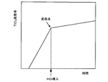
- It is a figure which shows the film-forming sequence which concerns on the 1st Embodiment of this invention. The state of the adsorption rate of TiCl 4 before and after the introduction of HCl is shown. It is a figure for demonstrating the 2nd Embodiment of this invention. It is a figure which shows the film-forming sequence which concerns on the 3rd Embodiment of this invention. It is a figure which shows the film-forming sequence which concerns on the 4th Embodiment of this invention.
- the substrate processing apparatus is configured as an example of a semiconductor manufacturing apparatus used for manufacturing a semiconductor device (IC Integrated Circuits).
- IC Integrated Circuits Integrated Circuits
- the substrate processing apparatus a case will be described in which a vertical apparatus that performs a film forming process or the like on a substrate is used.
- the present invention is not based on the use of a vertical apparatus, and for example, a single wafer apparatus may be used.
- the substrate processing apparatus 1 uses a cassette 100 that stores a wafer 200 as an example of a substrate, and the wafer 200 is made of a material such as silicon.
- the substrate processing apparatus 1 includes a housing 101, and a cassette stage 105 is installed inside the housing 101.
- the cassette 100 is carried on the cassette stage 105 by an in-process transfer device (not shown) or unloaded from the cassette stage 105.
- the cassette stage 105 is placed by the in-process transfer apparatus so that the wafer 200 in the cassette 100 maintains a vertical posture and the wafer loading / unloading port of the cassette 100 faces upward.
- the cassette stage 105 rotates the cassette 100 clockwise 90 ° to the rear of the casing 101 so that the wafer 200 in the cassette 100 is in a horizontal posture, and the wafer loading / unloading port of the cassette 100 faces the rear of the casing 101. It is configured to be operable.
- a cassette shelf 109 is installed at a substantially central portion in the front-rear direction in the housing 101, and the cassette shelf 109 is configured to store a plurality of cassettes 100 in a plurality of rows and a plurality of rows.
- the cassette shelf 109 is provided with a transfer shelf 123 in which the cassette 100 to be transferred by the wafer transfer mechanism 125 is stored.
- a reserve cassette shelf 110 is provided above the cassette stage 105, and is configured to store the cassette 100 preliminarily.
- a cassette transfer device 115 is installed between the cassette stage 105 and the cassette shelf 109.
- the cassette carrying device 115 includes a cassette elevator 115a that can move up and down while holding the cassette 100, and a cassette carrying mechanism 115b as a carrying mechanism.
- the cassette transport device 115 is configured to transport the cassette 100 among the cassette stage 105, the cassette shelf 109, and the spare cassette shelf 110 by continuous operation of the cassette elevator 115a and the cassette transport mechanism 115b.
- a wafer transfer mechanism 125 is installed behind the cassette shelf 109.
- the wafer transfer mechanism 125 includes a wafer transfer device 125a that can rotate or linearly move the wafer 200 in the horizontal direction, and a wafer transfer device elevator 125b that moves the wafer transfer device 125a up and down.
- the wafer transfer device 125 a is provided with a tweezer 125 c for picking up the wafer 200.
- the wafer transfer mechanism 125 loads (charges) the wafer 200 to the boat 217 by using the tweezers 125c as a placement portion of the wafer 200 by continuous operation of the wafer transfer device 125a and the wafer transfer device elevator 125b.
- the boat 217 is configured to be detached (discharged).
- a processing furnace 202 for heat-treating the wafer 200 is provided above the rear portion of the housing 101, and a lower end portion of the processing furnace 202 is configured to be opened and closed by a furnace port shutter 116.
- a boat elevator 121 that raises and lowers the boat 217 with respect to the processing furnace 202 is provided below the processing furnace 202.
- An arm 122 is connected to the lifting platform of the boat elevator 121, and a seal cap 219 is horizontally installed on the arm 122.
- the seal cap 219 is configured to support the boat 217 vertically and to close the lower end portion of the processing furnace 202.
- the boat 217 includes a plurality of holding members, and is configured to hold a plurality of (for example, about 50 to 150) wafers 200 horizontally with the centers thereof aligned in the vertical direction. Yes.
- the clean unit 134a for supplying clean air, which is a cleaned atmosphere, is installed.
- the clean unit 134 a includes a supply fan and a dustproof filter, and is configured to distribute clean air inside the housing 101.
- a clean unit 134 b for supplying clean air is installed at the left end of the housing 101.
- the clean unit 134b also includes a supply fan and a dustproof filter, and is configured to distribute clean air in the vicinity of the wafer transfer device 125a, the boat 217, and the like.
- the clean air is exhausted to the outside of the housing 101 after circulating in the vicinity of the wafer transfer device 125a, the boat 217, and the like.
- the cassette 100 When the cassette 100 is loaded onto the cassette stage 105 by an in-process transfer device (not shown), the cassette 100 holds the wafer 200 in a vertical position on the cassette stage 105 and the wafer loading / unloading port of the cassette 100 is directed upward. It is placed so that it faces. Thereafter, the cassette 100 is placed in a clockwise direction 90 in the clockwise direction behind the housing 101 so that the wafer 200 in the cassette 100 is placed in a horizontal posture by the cassette stage 105 and the wafer loading / unloading port of the cassette 100 faces the rear of the housing 101. ° Rotated.
- the cassette 100 is automatically transported and delivered to the designated shelf position of the cassette shelf 109 through the spare cassette shelf 110 by the cassette transport device 115, temporarily stored, and then stored in the cassette shelf 100 through the spare cassette shelf. It is transferred from 110 to the transfer shelf 123 by the cassette transfer device 115 or directly transferred to the transfer shelf 123.
- the wafer 200 is picked up from the cassette 100 through the wafer loading / unloading port by the tweezer 125c of the wafer transfer device 125a and loaded (charged) into the boat 217.
- the wafer transfer device 125 a that has delivered the wafer 200 to the boat 217 returns to the cassette 100 and loads the subsequent wafer 200 into the boat 217.
- the furnace port shutter 116 that has closed the lower end of the processing furnace 202 is opened, and the lower end of the processing furnace 202 is opened. Thereafter, the boat 217 holding the wafer group 200 is loaded into the processing furnace 202 by the ascending operation of the boat elevator 121, and the lower portion of the processing furnace 202 is closed by the seal cap 219.
- the processing furnace 202 is provided with a heater 207 which is a heating device (heating means) for heating the wafer 200.
- the heater 207 includes a cylindrical heat insulating member whose upper portion is closed and a plurality of heater wires, and has a unit configuration in which the heater wires are provided on the heat insulating member.
- a quartz reaction tube 203 for processing the wafer 200 is provided inside the heater 207.
- a manifold 209 made of stainless steel or the like is provided via an O-ring 220 that is an airtight member.
- the lower end opening of the manifold 209 is airtightly closed by a seal cap 219 as a lid through an O-ring 220.
- a processing chamber 201 is formed by at least the reaction tube 203, the manifold 209, and the seal cap 219.
- the seal cap 219 is provided with a boat support 218 that supports the boat 217.
- the boat 217 includes a bottom plate 210 fixed to the boat support base 218 and a top plate 211 disposed above the bottom plate 210, and a plurality of support columns are disposed between the bottom plate 210 and the top plate 211.
- 221 has a construction in which it is installed.
- a plurality of wafers 200 are held on the boat 217.
- the plurality of wafers 200 are supported by the column 221 of the boat 217 in a state where the wafer 200 is maintained in a horizontal posture while being spaced apart from each other.
- the boat 217 in a state where a plurality of batch-processed wafers 200 are stacked on the boat 217, the boat 217 is inserted into the processing chamber 201 while being supported by the boat support 218, and the heater 207 is The wafer 200 inserted into the processing chamber 201 is heated to a predetermined temperature.
- two gas supply pipes 310 and 320 (first gas supply pipe 310 and second gas supply pipe 320) for supplying source gas are connected to the processing chamber 201. Has been.
- the gas supply pipe 310 is provided with a mass flow controller 312 that is a flow rate control device (flow rate control means), a vaporizer 700 that is a vaporization unit (vaporization means), and a valve 314 that is an on-off valve in order from the upstream side.
- a nozzle 410 (first nozzle 410) is connected to the tip of the gas supply pipe 310.
- the first nozzle 410 is an arc-shaped space between the inner wall of the reaction tube 203 constituting the processing chamber 201 and the wafer 200, and the vertical direction along the inner wall of the reaction tube 203 (the loading direction of the wafer 200). It extends to.
- On the side surface of the first nozzle 410 a large number of gas supply holes 410a for supplying a source gas are provided.
- the gas supply holes 410a have the same or inclined opening areas from the lower part to the upper part, and are provided at the same opening pitch.
- the gas supply pipe 310 is provided with a vent line 610 and a valve 614 connected to an exhaust pipe 231 described later between the vaporizer 700 and the valve 314, and the source gas is not supplied to the processing chamber 201. Supplies the source gas to the vent line 610 via the valve 614.
- a gas supply pipe 310, a mass flow controller 312, a vaporizer 700, a valve 314, a first nozzle 410, a vent line 610, and a valve 614 constitute a first gas supply system (first source gas supply system).
- a carrier gas supply pipe 510 for supplying a carrier gas is connected to the gas supply pipe 310.
- the carrier gas supply pipe 510 is provided with a mass flow controller 512 and a valve 514.
- the carrier gas supply pipe 510, the mass flow controller 512, and the valve 514 mainly constitute a first carrier gas supply system (first inert gas supply system).
- the gas supply pipe 320 is provided with a mass flow controller 322 and a valve 324 which are flow rate control devices (flow rate control means) in order from the upstream side.
- a nozzle 420 (second nozzle 420) is connected to the distal end portion of the gas supply pipe 320.
- the second nozzle 420 is an arc-shaped space between the inner wall of the reaction tube 203 constituting the processing chamber 201 and the wafer 200, along the inner wall of the reaction tube 203. It extends in the vertical direction (the loading direction of the wafer 200).
- the gas supply holes 420a have the same or inclined opening areas from the lower part to the upper part, and are provided at the same opening pitch.
- the gas supply pipe 320, the mass flow controller 322, the valve 324, and the second nozzle 420 mainly constitute a second gas supply system (reformed gas supply system, reaction gas supply system).
- a carrier gas supply pipe 520 for supplying a carrier gas is connected to the gas supply pipe 320.
- the carrier gas supply pipe 520 is provided with a mass flow controller 522 and a valve 524.
- the carrier gas supply pipe 520, the mass flow controller 522, and the valve 524 mainly constitute a second carrier gas supply system (second inert gas supply system).
- a gas supply pipe 710 is connected to the gas supply pipe 310 on the downstream side of the junction between the gas supply pipe 310 and the carrier gas supply pipe 510.
- the gas supply pipe 710 is provided with a mass flow controller 712 and a valve 714.
- the gas supply pipe 710, the mass flow controller 712, and the valve 714 mainly constitute a third gas supply system (first Cl-containing gas supply system).
- a gas supply pipe 720 is connected to the gas supply pipe 320 on the downstream side of the junction of the gas supply pipe 320 and the carrier gas supply pipe 520.
- the gas supply pipe 720 is provided with a mass flow controller 722 and a valve 724.
- a gas supply pipe 720, a mass flow controller 722, and a valve 724 mainly constitute a fourth gas supply system (second Cl-containing gas supply system). In some cases, the fourth gas supply system may not be provided.
- the gas supply pipe 310 merges with the carrier gas supply pipe 510 via the mass flow controller 312, the vaporizer 700, and the valve 314, and further the gas supply pipe 710. Then, the reaction gas is supplied into the processing chamber 201 through the first nozzle 410.
- the mass flow controller 312 is replaced with a gas mass flow controller, and the vaporizer 700 becomes unnecessary.
- the gas supply pipe 320 merges with the carrier gas supply pipe 520 via the mass flow controller 322 and the valve 324, and further merges with the gas supply pipe 720, and then enters the processing chamber 201 via the second nozzle 420. Is supplied.
- the gas supply pipe 310 includes, for example, a titanium (Ti) -containing raw material (titanium tetrachloride (TiCl 4 ) or tetrakisdimethylaminotitanium (TDMAT), which is a metal raw material, as the first raw material gas.
- Ti titanium tetrachloride
- TDMAT tetrakisdimethylaminotitanium
- the gas supply pipe 320 includes an O-containing gas or an N-containing gas such as ammonia (NH 3 ), nitrogen (N 2 ), nitrogen, or the like, which is an O-containing gas or an N-containing gas as a reformed gas for reforming the raw material gas that is the first raw material.
- Nitrogen oxide (N 2 O), monomethylhydrazine (CH 6 N 2 ) or the like is introduced.
- hydrogen chloride (HCl), chlorine (Cl 2 ) or the like which is a Cl-containing gas, is introduced into the gas supply pipes 710 and 720 as a reaction gas to be reacted with the first raw material.
- the reaction tube 203 is provided with an exhaust pipe 231 for exhausting the atmosphere in the processing chamber 201.
- the exhaust pipe 231 is evacuated through a pressure detector (a pressure sensor 245 as a pressure detector and an APC (Auto Pressure Controller) valve 243 as a pressure regulator) for detecting the pressure in the processing chamber 201.
- a vacuum pump 246 as an apparatus (exhaust means) is connected, and is configured to be evacuated so that the pressure in the processing chamber 201 becomes a predetermined pressure (degree of vacuum).
- a temperature sensor 263 as a temperature detector is installed in the reaction tube 203, and the temperature in the processing chamber 201 is adjusted by adjusting the power supply to the heater 207 based on the temperature information detected by the temperature sensor 263. It is configured to have a desired temperature distribution.
- the temperature sensor 263 is configured in an L shape similarly to the nozzles 410 and 420, and is provided along the inner wall of the reaction tube 203.
- a boat 217 is provided in the center of the reaction tube 203.
- a boat rotation mechanism 267 that rotates the boat 217 is provided at the lower end of the boat support 218 that supports the boat 217 in order to improve processing uniformity.
- a rotation shaft 255 of the rotation mechanism 267 passes through the seal cap 219 and is connected to the boat 217, and is configured to rotate the wafer 200 by rotating the boat 217.
- the seal cap 219 is configured to be moved up and down in the vertical direction by a boat elevator 121 provided outside the reaction tube 203, so that the boat 217 can be carried into and out of the processing chamber 201. Yes.
- the controller 280 is an example of a control unit (control means) that controls the overall operation of the substrate processing apparatus 1.
- the controller 280 adjusts the flow rate of the mass flow controllers 312, 322, 512, 522, 712, 722, valves 314, 324, 514.
- TiCl 4 is used as a raw material gas containing titanium (Ti)
- NH 3 is used as a nitriding raw material that is a reformed gas
- HCl is used as a Cl-containing gas that is a reactive gas.
- FIG. 4 shows a film forming sequence of the titanium nitride film according to this embodiment.
- the controller 280 controls the substrate processing apparatus 1 as follows.
- the heater 207 is controlled to set the inside of the processing chamber 201 to a temperature in the range of 200 ° C. to 650 ° C., for example, and preferably 300 ° C. to 500 ° C.
- a plurality of wafers 200 are loaded into the boat 217, and the boat 217 is loaded into the processing chamber 201.
- the boat 217 is rotated by the boat driving mechanism 267 to rotate the wafer 200.
- the vacuum pump 246 is operated and the valve 243 is opened to evacuate the inside of the processing chamber 201.
- the temperature of the wafer 200 is, for example, in the range of 200 ° C. to 650 ° C., preferably 300 ° C. to 500 ° C.
- the sequence described later is performed in the state held in the above.
- Step 11 TiCl 4 is flowed.
- TiCl 4 is a liquid at room temperature, and is supplied to the processing chamber 201 by heating and vaporizing and supplying, He (helium), Ne (neon), called carrier gas using the vaporizer 700,
- He helium
- Ne neon
- carrier gas a gas such as He (helium), Ne (neon), called carrier gas using the vaporizer 700.
- an inert gas such as Ar (argon) or N 2 (nitrogen) is passed through a TiCl 4 container and the vaporized portion is supplied to the processing chamber 201 together with the carrier gas. The case will be described.
- TiCl 4 is passed through the gas supply pipe 310 and carrier gas (N 2 ) is passed through the carrier gas supply pipe 510.
- carrier gas N 2
- the valve 314 of the gas supply pipe 310, the valve 514 of the carrier gas supply pipe 510, and the APC valve 243 of the exhaust pipe 231 are all opened.
- the carrier gas flows from the carrier gas supply pipe 510 and the flow rate is adjusted by the mass flow controller 512.
- TiCl 4 flows from the gas supply pipe 310, the flow rate of which is adjusted by the mass flow controller 312, the vaporized gas of the vaporizer 700, and the carrier gas of which the flow rate is adjusted are mixed and supplied into the processing chamber 201 from the gas supply hole 410 a of the nozzle 410.
- the exhaust pipe 231 is exhausted while being exhausted.
- the APC valve 243 is appropriately adjusted to maintain the pressure in the processing chamber 201 within a range of 20 to 100 Pa, for example, 30 Pa.
- the supply amount of TiCl 4 controlled by the mass flow controller 312 is 1.0 to 2.0 g / min.
- the time for exposing the wafer 200 to TiCl 4 is 3 to 10 seconds.
- the temperature of the heater 207 is set so that the wafer temperature is in the range of 200 ° C. to 650 ° C., preferably 300 ° C. to 500 ° C., for example, 380 ° C.
- the gases flowing into the processing chamber 201 are only inert gases such as TiCl 4 , N 2 , and Ar, and NH 3 and HCl do not exist. Therefore, TiCl 4 does not cause a gas phase reaction, and reacts with the surface of the wafer 200 and the underlying film (chemical adsorption) to form an adsorption layer or a Ti layer (hereinafter referred to as a Ti-containing layer) of the raw material (TiCl 4 ).
- the adsorption layer of TiCl 4 includes a continuous adsorption layer of raw material molecules and a discontinuous adsorption layer.
- the Ti layer includes not only a continuous layer composed of Ti but also a Ti thin film formed by overlapping these layers.
- the continuous layer comprised by Ti may be called Ti thin film.
- the inert gas is flowed from the carrier gas supply pipe 520 connected to the middle of the gas supply pipe 320 by opening the valve 524.
- TiCl 4 can be prevented from entering the NH 3 side.
- Step 12 HCl is flowed. HCl serves to suppress the growth of TiN. HCl is passed through the gas supply pipe 710. The valve 714 of the gas supply pipe 710 is opened. The TiCl 4 that has been mixed and supplied from the gas supply pipe 310 with the carrier gas is mixed with HCl whose flow rate has been adjusted by the mass flow controller 712, and is supplied into the processing chamber 201 from the gas supply hole 410a of the nozzle 410 while being exhausted. 231 is exhausted.
- an inert gas such as N 2 is continuously supplied into the processing chamber 201 from the gas supply hole 420 a of the nozzle 420.
- Step 13 The valve 314 of the gas supply pipe 310 is closed to stop the supply of TiCl 4 to the processing chamber, and the valve 614 is opened to flow TiCl 4 to the vent line 610. Accordingly, only HCl mixed with the carrier gas is supplied from the gas supply hole 410a of the nozzle 410.
- the APC valve 243 is appropriately adjusted to maintain the pressure in the processing chamber 201 within a range of 10 to 50 Pa, for example, 20 Pa.
- the supply flow rate of HCl controlled by the mass flow controller 712 is 0.5 to 5 slm.
- the time for exposing the wafer 200 to HCl is 1 to 5 seconds.
- the temperature of the heater 207 at this time is set so that the wafer temperature is in the range of 200 ° C. to 650 ° C., preferably 300 ° C. to 500 ° C., for example, 380 ° C.
- Step 14 The valve 714 of the gas supply pipe 710 is closed, and supply of HCl into the processing chamber 201 is stopped. At this time, the APC valve 243 of the gas exhaust pipe 231 is kept open, and the inside of the processing chamber 201 is exhausted to 10 Pa or less by the vacuum pump 246 to remove the residual TiCl 4 from the processing chamber 201. At this time, an inert gas such as N 2 is continuously supplied into the processing chamber 201 from the gas supply hole 420 a of the nozzle 420. This further increases the effect of eliminating residual TiCl 4 .
- Step 15 NH 3 is flowed.
- NH 3 flows through the gas supply pipe 320 and carrier gas (N 2 ) flows through the carrier gas supply pipe 520.
- the valve 324 of the gas supply pipe 320, the valve 522 of the carrier gas supply pipe 520, and the APC valve 243 of the exhaust pipe 231 are all opened.
- the carrier gas flows from the carrier gas supply pipe 520 and the flow rate is adjusted by the mass flow controller 522.
- NH 3 flows from the gas supply pipe 320, is adjusted in flow rate by the mass flow controller 322, mixes the adjusted carrier gas, and is exhausted from the exhaust pipe 231 while being supplied from the gas supply hole 420 a of the nozzle 420 into the processing chamber 201. Is done.
- the APC valve 243 When flowing NH 3 , the APC valve 243 is appropriately adjusted to maintain the pressure in the processing chamber 201 within a range of 50 to 1000 Pa, for example, 60 Pa.
- the supply flow rate of NH 3 controlled by the mass flow controller 324 is 1 to 10 slm.
- the time for exposing the wafer 200 to NH 3 is 10 to 45 seconds.
- the temperature of the heater 207 at this time is set so that the wafer temperature is in the range of 200 ° C. to 650 ° C., preferably 300 ° C. to 500 ° C., for example, 380 ° C.
- the Ti-containing layer chemically adsorbed on the wafer 200 and NH 3 undergo a surface reaction (chemical adsorption), and a titanium nitride film is formed on the wafer 200.
- Step 16 the APC valve 324 of the gas supply pipe 320 is closed to stop the supply of NH 3 . Further, the APC valve 243 of the gas exhaust pipe 231 is kept open, the processing chamber 201 is exhausted to 10 Pa or less by the vacuum pump 246, and residual NH 3 is removed from the processing chamber 201. At this time, if inert gas such as N 2 is supplied to the processing chamber 201 from the gas supply pipe 320 that is an NH 3 supply line and the gas supply pipe 310 that is a TiCl 4 supply line and is purged, residual NH 3 The effect of eliminating is further enhanced.
- inert gas such as N 2
- the above steps 11 to 16 are defined as one cycle, and a titanium nitride film having a predetermined thickness is formed on the wafer 200 by performing at least once.
- TiCl 4 As described above, by introducing TiCl 4 into the processing chamber 201, TiCl 4 is adsorbed on the adsorption sites on the wafer 200, and the surface of the wafer 200 is gradually covered with TiClx.
- the required time varies depending on the environmental temperature, the introduction flow rate, the pressure, etc., but is approximately several seconds to several tens of seconds.
- HCl that is a reaction suppressing substance is introduced in a state where TiCl 4 is introduced at a timing (before saturation) before TiCl 4 is adsorbed on all adsorption sites.
- the introduced HCl fills a part of the adsorption site, and the adsorption of TiCl 4 is inhibited.
- NH 3 is introduced. This NH 3 reacts with TiClx on the surface of the substrate to be processed to grow TiN and at the same time has a function of desorbing HCl from the surface. Further, after removing excess NH 3 in the processing chamber 201, a high-quality TiN film can be obtained by repeating the above processing until a desired film thickness is obtained.
- the amount of Ti adsorbed on the substrate is reduced by supplying HCl as a reaction inhibitor, and then NH 3 is supplied to react with a sufficient amount of nitrogen. As a result, a more nitrogen-rich film is formed, and the resistivity of the film is considered to be low.
- the reaction-inhibiting substance is introduced into the processing chamber 201 to realize the continuous film formation of less than one atomic layer.
- the reaction-inhibiting substance is not introduced, and the reaction gas and the reaction conditions are optimized.
- the by-product is used for reaction suppression.
- the amount of film formation at the inflection point can be controlled by controlling the film formation temperature or pressure.
- TiCl 4 is used as a raw material gas containing titanium (Ti) and NH 3 is used as a nitriding raw material that is a reformed gas.
- the controller 280 controls the substrate processing apparatus 1 as follows, as in the first embodiment. That is, by controlling the heater 207, the inside of the processing chamber 201 is set to a temperature in the range of 250 ° C. to 450 ° C., and the pressure in the processing chamber 201 is maintained at 10 Pa to 100 Pa.
- FIG. 6 shows an example in which a TiN film is formed using the above-described conditions. As shown in FIG. 6, the amount of film formation per time obtained by dividing the final film thickness by the number of times of sequential film formation using the introduction time of TiCl 4 per time of sequential film formation as a parameter is 1 atom.
- the atomic layer of TiN crystal in the low-order plane orientation is about 1 to 3 mm, and in this example, about 1/10 to 1/4 atomic layer was formed per one sequential film formation. I understand.
- FIG. 7 shows a film forming sequence of the titanium nitride film according to the third embodiment. In the third embodiment, only portions different from the first embodiment will be described.
- Step 21 TiCl 4 is supplied to the processing chamber via the nozzle 410 under the same conditions as in step 11. At this time, an inert gas such as N 2 is supplied from the nozzle 420 to the processing chamber.
- Step 22 As in Step 12, with TiCl 4 supplied to the processing chamber, HCl is supplied from the gas supply pipe 710 to the processing chamber via the nozzle 410. At this time, an inert gas such as N 2 is continuously supplied from the nozzle 420 to the processing chamber.
- Step 23 As in step 13, with HCl supplied to the processing chamber, the valve 314 of the gas supply pipe 310 is closed to stop the supply of TiCl 4 to the processing chamber, and the valve 614 is opened to allow TiCl 4 to flow into the vent line 610.
- Step 24 As in step 14, the valve 714 of the gas supply pipe 710 is closed to stop the supply of HCl to the processing chamber. At this time, the APC valve 243 of the gas exhaust pipe 231 is kept open, and the inside of the processing chamber 201 is evacuated to 20 Pa or less by the vacuum pump 246 to remove residual TiCl 4 from the processing chamber 201. At this time, if an inert gas such as N 2 is supplied from the nozzle 420 into the processing chamber 201, the effect of removing residual TiCl 4 is further enhanced.
- an inert gas such as N 2
- Step 25 NH 3 is supplied to the processing chamber under the same conditions as in step 15. NH 3 flows through the gas supply pipe 320 and carrier gas (N 2 ) flows through the carrier gas supply pipe 520.
- Step 26 the valve 324 of the gas supply pipe 320 is closed to stop the supply of NH 3 . Further, the APC valve 243 of the gas exhaust pipe 231 is kept open, the processing chamber 201 is exhausted to 20 Pa or less by the vacuum pump 246, and residual NH 3 is removed from the processing chamber 201.
- Step 27 NH 3 is again supplied to the processing chamber and light or plasma is irradiated. NH 3 is allowed to flow under the same conditions as in step 15 and step 25, for example.
- Step 28 the valve 324 of the gas supply pipe 320 is closed to stop the supply of NH 3 . Further, the APC valve 243 of the gas exhaust pipe 231 is kept open, the processing chamber 201 is exhausted to 20 Pa or less by the vacuum pump 246, and residual NH 3 is removed from the processing chamber 201.
- Steps 21 to 28 are defined as one cycle, and a predetermined number of times is performed at least once to form a titanium nitride film having a predetermined thickness on the wafer 200.
- a predetermined number of times is performed at least once to form a titanium nitride film having a predetermined thickness on the wafer 200.
- FIG. 8 shows a film forming sequence of the titanium nitride film according to the fourth embodiment. In the fourth embodiment, only portions different from the first embodiment will be described.
- Step 31 TiCl 4 is supplied to the processing chamber under the same conditions as in step 11. At this time, the temperature of the heater 207 is set so that the wafer temperature is in the range of 200 ° C. to 550 ° C., preferably 350 ° C. to 450 ° C., for example, 380 ° C.
- Step 32 As in Step 12, with TiCl 4 supplied to the processing chamber, HCl is supplied from the gas supply pipe 710 to the processing chamber via the nozzle 410. At this time, an inert gas such as N 2 is continuously supplied from the nozzle 420 to the processing chamber.
- Step 33 As in step 13, with HCl supplied to the processing chamber, the valve 314 of the gas supply pipe 310 is closed to stop the supply of TiCl 4 to the processing chamber, and the valve 614 is opened to allow TiCl 4 to flow into the vent line 610.
- Step 34 As in step 14, the valve 714 of the gas supply pipe 710 is closed to stop the supply of HCl to the processing chamber. At this time, the APC valve 243 of the gas exhaust pipe 231 is kept open, and the inside of the processing chamber 201 is evacuated to 10 Pa or less by the vacuum pump 246 to remove residual TiCl 4 from the processing chamber 201. At this time, if an inert gas such as N 2 is supplied into the processing chamber 201, the effect of removing residual TiCl 4 is further enhanced.
- an inert gas such as N 2
- Step 35 NH 3 is supplied under the same conditions as in step 15. NH 3 flows through the gas supply pipe 320 and carrier gas (N 2 ) flows through the carrier gas supply pipe 520.
- Step 36 the valve 324 of the gas supply pipe 320 is closed to stop the supply of NH 3 . Further, the APC valve 243 of the gas exhaust pipe 231 is kept open, the processing chamber 201 is exhausted to 20 Pa or less by the vacuum pump 246, and residual NH 3 is removed from the processing chamber 201.
- step 37 temperature increase in the processing chamber is started.
- Step 38 In step 38, NH 3 is supplied again. NH 3 is allowed to flow under the same conditions as in steps 15 and 25. At this time, the temperature of the heater 207 is set so that the wafer temperature is in the range of 300 ° C. to 650 ° C., preferably 400 ° C. to 650 ° C., for example, 650 ° C.
- Step 39 In step 39, the valve 324 of the gas supply pipe 320 is closed, the supply of NH 3 is stopped, and the temperature in the processing chamber is lowered.
- Step 40 The temperature in the treatment chamber is in the range of 200 ° C. to 550 ° C., preferably 350 ° C. to 450 ° C.
- the APC valve 243 of the gas exhaust pipe 231 is kept open, the processing chamber 201 is exhausted to 10 Pa or less by the vacuum pump 246, and residual NH 3 is removed from the processing chamber 201.
- the above steps 31 to 40 are defined as one cycle, and a titanium nitride film having a predetermined thickness is formed on the wafer 200 by performing at least once and a predetermined number of times.
- a titanium nitride film having a predetermined thickness is formed on the wafer 200 by performing at least once and a predetermined number of times.
- separation of the reaction inhibitor is promoted, and NH 3 is introduced so that nitriding proceeds even when unreacted Ti is scattered.
- the temperature increase and the NH 3 introduction are performed at the same time.
- HCl which is a reaction inhibitor
- HCl is not supplied from outside the processing chamber, and reaction by-products are generated in the processing chamber. This process is effective even when HCl generated as a product is supplied to the surface of the wafer 200.
- reaction-suppressing substance may be supplied from all nozzles (for example, nozzle 410 and nozzle 420).
- the present invention it is possible to suppress the residue of impurities in the film by performing the further sequential film formation as compared with the ALD method. Furthermore, since the surface layer of the thin film that is the target for modification can be made thinner, more effective film quality improvement can be performed.
- a portion where growth of less than one atomic layer has occurred is described as a thin film or layer for the sake of convenience, and the growth of less than one atomic layer here is a thin film having an originally assumed plane orientation.
- the number of atoms per unit area contained in a thin film grown by one sequential film formation is smaller than the number of atoms per unit area for constituting one atomic layer.
- the vertical apparatus has been mainly described.
- the formation of the titanium nitride film using at least two or more different CVD methods in the present invention is not limited to the vertical apparatus, but other devices such as a single wafer apparatus. It is also applicable to the device.
- the vertical thermal CVD apparatus has been mainly described.
- the formation of the titanium nitride film using at least two or more different CVD methods in the present invention is not limited to the thermal CVD apparatus, but a plasma CVD apparatus.
- the present invention can also be applied to other apparatuses such as a photo-CVD apparatus.
- titanium nitride film is formed on a substrate by reacting titanium tetrachloride (TiCl 4 ) with ammonia (NH 3 )
- TiCl 4 titanium tetrachloride
- NH 3 ammonia
- the present invention is not limited to this, and other film types are used. Is also applicable.
- the present invention is applicable to nitrides such as titanium nitride (TiN) and tantalum nitride (TaN) and metal compounds to which elements are mainly added.
- the method of manufacturing a semiconductor device that forms a film of less than one atomic layer on the surface of the substrate is provided.
- the reaction gas is a Cl-containing gas.
- the first raw material is a metal raw material
- the reformed gas is an O-containing gas or an N-containing gas.
- the reformed gas is activated by using heat, light, or plasma.
- the temperature of the substrate is set to 200 to 550 ° C.
- the temperature of the substrate is set to 300 to 450 ° C.
- the temperature of the substrate is set to be equal to or lower than the self-decomposition temperature of the first raw material.
- the first raw material is supplied to the processing chamber in which the substrate is accommodated to adsorb the first raw material less than one atomic layer on the surface of the substrate. And a second step of supplying a reforming gas for reforming the first raw material adsorbed on the surface of the substrate to the processing chamber, thereby forming a single atomic layer on the surface of the substrate.
- a third step of removing the atmosphere in the processing chamber, and a reforming gas for reforming the first raw material is supplied to the processing chamber to reform the first raw material adsorbed on the substrate.
- a fourth step of removing the atmosphere in the processing chamber; a reforming gas supplied to the processing chamber while activating the reformed gas; and reforming the first raw material adsorbed on the substrate A semiconductor device that forms a film of less than one atomic layer on the surface of the substrate by sequentially performing the sixth step Manufacturing method is provided. (Appendix 10) According to another aspect of the present invention, the first raw material is supplied to the surface of the substrate while supplying the first raw material to the processing chamber in which the substrate is accommodated at the first temperature.
- Appendix 11 Preferably, a film having less than one atomic layer is formed on the surface of the substrate by providing an inflection point in the growth rate of the film.
- Appendix 12 a semiconductor device manufactured using any one of the manufacturing methods of the semiconductor device described in Appendix 1 to Appendix 11 is provided.
- a processing chamber that accommodates a substrate, a source gas supply system that supplies a source gas containing a first element to the processing chamber, and the first element in the processing chamber
- a reaction gas supply system that supplies a reaction gas that reacts with the gas
- a Cl-containing gas supply system that supplies a Cl-containing gas to the processing chamber
- an exhaust system that exhausts the processing chamber, the source gas supply system, and the reaction gas
- a control unit that controls a supply system, the Cl-containing gas supply system, and the exhaust system, wherein the control unit includes the source gas supply system, the reaction gas supply system, the Cl-containing gas supply system, and the exhaust gas.
- the system is controlled to supply the first source gas to adsorb at least the first element on the surface of the substrate, and the reactive gas before the first source is saturated and adsorbed on the surface of the substrate.
- a substrate processing apparatus is provided for forming a film of less than one atomic layer on the surface of the substrate.
- Substrate processing apparatus 200 Wafer 201 Processing chamber 202 Processing furnace 203 Reaction tube 207 Heater 217 Boat 218 Boat support 231 Exhaust pipe 243 APC valve 246 Vacuum pump 267 Boat rotation mechanism 280 Controller 410, 420 Nozzle 410a, 420a Gas supply hole
Abstract
Disclosed is a technique for forming a dense metal film which has low resistivity and low concentrations of impurities that are derived from starting materials.
Specifically disclosed is a method for manufacturing a semiconductor device, wherein a film less than one atomic layer is formed on the surface of a substrate by carrying out: a first step wherein a first starting material is supplied into a process chamber, in which the substrate is contained, and the surface of the substrate is caused to adsorb the first starting material; a second step wherein a reaction gas, which is different from the first starting material, is supplied into the process chamber before the adsorption of the first starting material on the substrate surface is saturated, and is caused to react with the first starting material adsorbed on the substrate; a third step wherein the atmosphere within the process chamber is removed; and a fourth step wherein a modifying gas for modifying the first starting material is supplied into the process chamber and the first starting material adsorbed on the substrate is modified.
Description
本発明は、半導体装置の製造方法及び基板処理装置に関し、特に、基板(ウエハ)上に金属膜を形成する工程を備える半導体装置の製造方法及び基板処理装置に関する。
The present invention relates to a semiconductor device manufacturing method and a substrate processing apparatus, and more particularly to a semiconductor device manufacturing method and a substrate processing apparatus including a step of forming a metal film on a substrate (wafer).
基板上に所定の膜を形成する手法の1つとして、CVD(Chemical Vapor Deposition)法がある。CVD法とは、気相中もしくは基板表面における2種以上の原料の反応を利用して、原料分子に含まれる元素を構成要素とする膜を基板上に成膜する方法である。また、他の手法として、ALD(Atomic Layer Deposition)法がある。ALD法とは、ある成膜条件(温度、時間等)の下で、成膜に用いる2種以上の原料となる原料を1種類ずつ交互に基板上に供給し、原子層単位で吸着させ、表面反応を利用して原子層レベルで制御される成膜を行う手法である。ALD法では、より低い基板温度(処理温度)で処理が可能であり、原料ガスを交互に供給し、基板上に原料ガスを吸着させることにより原子層1層毎に成膜を繰り返すことができて、成膜サイクル回数によって成膜される膜厚の制御が可能である。
また、基板上に形成される金属膜としては、例えば、特許文献1のように窒化チタン(TiN)膜が挙げられる。 One of the methods for forming a predetermined film on a substrate is a CVD (Chemical Vapor Deposition) method. The CVD method is a method in which a film containing an element contained in a raw material molecule as a constituent element is formed on a substrate by utilizing a reaction of two or more raw materials in a gas phase or on the substrate surface. As another method, there is an ALD (Atomic Layer Deposition) method. The ALD method is a method in which two or more kinds of raw materials used for film formation are alternately supplied onto a substrate under a certain film formation condition (temperature, time, etc.) and adsorbed in units of atomic layers. This is a technique for performing film formation controlled at the atomic layer level using surface reaction. In the ALD method, processing can be performed at a lower substrate temperature (processing temperature), and film formation can be repeated for each atomic layer by alternately supplying source gases and adsorbing source gases on the substrate. Thus, the film thickness can be controlled by the number of film formation cycles.
Moreover, as a metal film formed on a board | substrate, a titanium nitride (TiN) film | membrane is mentioned like patent document 1, for example.
金属膜として被処理基板上に窒化チタン膜を成膜するとき、例えばチタン(Ti)含有原料として四塩化チタン(TiCl4)を用い、窒化ガスとしてアンモニア(NH3)を用いる場合があるが、CVD法により成膜するとALD法で成膜した場合と比較して、膜中に塩素(Cl)が取り込まれやすいなどの理由により、抵抗率の上昇を招いてしまうなどの問題がある。
When a titanium nitride film is formed on a substrate to be processed as a metal film, for example, titanium tetrachloride (TiCl 4 ) is used as a raw material containing titanium (Ti) and ammonia (NH 3 ) is used as a nitriding gas. When the film is formed by the CVD method, there is a problem that the resistivity is increased due to the fact that chlorine (Cl) is easily taken into the film as compared with the case where the film is formed by the ALD method.
一方、ALD法にて成膜した窒化チタン膜の連続膜は、CVD法で成膜した場合と比較し、滑らかな表面が得られ、且つ塩素濃度が低く比較的抵抗値の低い窒化チタン膜を得ることが出来る。
しかし、窒化チタン膜に対する要求性能の向上に従って、更なる不純物の低減や低抵抗化などの高品質化が求められている。
このような例は窒化チタン膜に留まらず、金属化合物の形成において一般的な課題となっている。例えば、有機金属材料を用いて高誘電率の金属酸化膜を成膜する場合、材料中の炭素(C)が膜中に残留することにより、絶縁耐性を劣化させる等の問題も顕在化している。 On the other hand, a continuous film of a titanium nitride film formed by the ALD method has a smooth surface and a titanium nitride film having a low chlorine concentration and a relatively low resistance value as compared with the case of forming by the CVD method. Can be obtained.
However, as the required performance of the titanium nitride film is improved, higher quality such as further reduction of impurities and lower resistance is required.
Such an example is not limited to the titanium nitride film, but is a general problem in the formation of metal compounds. For example, when a metal oxide film having a high dielectric constant is formed using an organometallic material, problems such as deterioration of insulation resistance due to carbon (C) remaining in the film have become apparent. .
従って、本発明の主な目的は、上記問題を解決し、緻密で原料起因の不純物濃度が低く抵抗率の低い金属膜を形成する半導体装置の製造方法及び基板処理装置を提供することである。
Therefore, a main object of the present invention is to provide a semiconductor device manufacturing method and a substrate processing apparatus for solving the above-mentioned problems and forming a dense metal film having a low impurity concentration due to raw materials and a low resistivity.
上記課題を解決するため、本発明の一態様によれば、基板が収容された処理室に、第1の原料を供給して前記基板の表面に前記第1の原料を吸着させる第1の工程と、前記第1の原料が前記基板の表面で飽和吸着する前に、前記処理室に前記第1の原料とは異なる反応ガスを供給して、前記基板に吸着した第1の原料と反応させる第2の工程と、前記処理室内の雰囲気を除去する第3の工程と、前記処理室に前記第1の原料を改質する改質ガスを供給して、前記基板に吸着した前記第1の原料を改質する第4の工程と、を行うことで前記基板の表面に1原子層未満の膜を形成する半導体装置の製造方法が提供される。
In order to solve the above-described problem, according to one aspect of the present invention, a first process of supplying a first raw material to a processing chamber in which a substrate is accommodated and adsorbing the first raw material on the surface of the substrate. In addition, before the first raw material is saturated and adsorbed on the surface of the substrate, a reactive gas different from the first raw material is supplied to the processing chamber to react with the first raw material adsorbed on the substrate. A second step; a third step of removing an atmosphere in the processing chamber; and supply of a reforming gas for reforming the first raw material to the processing chamber, so that the first adsorbed on the substrate And a fourth step of modifying the raw material, thereby providing a method of manufacturing a semiconductor device that forms a film of less than one atomic layer on the surface of the substrate.
本発明の他の態様によれば、基板が収容された処理室に、第1の原料を供給して前記基板の表面に前記第1の原料を吸着させる第1の工程と、前記第1の原料が前記基板の表面で飽和吸着する前に、前記処理室に前記第1の原料とは異なる反応ガスを供給して、前記基板に吸着した第1の原料と反応させる第2の工程と、前記処理室内の雰囲気を除去する第3の工程と、前記処理室に前記第1の原料を改質する改質ガスを供給して、前記基板に吸着した前記第1の原料を改質する第4の工程と、前記処理室内の雰囲気を除去する第5の工程と、前記改質ガスを活性化しつつ前記処理室に供給して、前記基板に吸着した前記第1の原料を改質する第6の工程と、を順に行うことで前記基板の表面に1原子層未満の膜を形成する半導体装置の製造方法が提供される。
According to another aspect of the present invention, a first step of supplying a first raw material to a processing chamber in which a substrate is accommodated to adsorb the first raw material on the surface of the substrate; A second step of supplying a reactive gas different from the first raw material to the processing chamber and reacting with the first raw material adsorbed on the substrate before the raw material is saturated and adsorbed on the surface of the substrate; A third step of removing the atmosphere in the processing chamber; and a reforming gas for reforming the first raw material is supplied to the processing chamber to reform the first raw material adsorbed on the substrate. And a fifth step of removing the atmosphere in the processing chamber, and a step of reforming the first raw material adsorbed on the substrate by supplying the reformed gas to the processing chamber while activating the reformed gas. 6 is sequentially performed to manufacture a semiconductor device that forms a film of less than one atomic layer on the surface of the substrate. A method is provided.
本発明の他の態様によれば、基板が収容された処理室に、第1の温度で前記基板を加熱しつつ、第1の原料を供給して前記基板の表面に前記第1の原料を吸着させる第1の工程と、前記第1の原料が前記基板の表面で飽和吸着する前に、前記処理室に前記第1の原料とは異なる反応ガスを供給して、前記基板に吸着した第1の原料と反応させる第2の工程と、前記処理室内の雰囲気を除去する第3の工程と、前記第1の温度より高い第2の温度で前記基板を加熱しつつ、前記処理室に前記第1の原料を改質する改質ガスを供給して、前記基板に吸着した前記第1の原料を改質する第4の工程と、を行うことで前記基板の表面に1原子層未満の膜を形成する半導体装置の製造方法が提供される。
According to another aspect of the present invention, the first raw material is supplied to the surface of the substrate by supplying the first raw material to the processing chamber containing the substrate while heating the substrate at a first temperature. A first step of adsorbing and supplying a reactive gas different from the first raw material to the processing chamber before the first raw material is saturated and adsorbed on the surface of the substrate, A second step of reacting with one raw material, a third step of removing the atmosphere in the processing chamber, and heating the substrate at a second temperature higher than the first temperature, A reforming gas for reforming the first material and a fourth step for reforming the first material adsorbed on the substrate, so that the surface of the substrate is less than one atomic layer. A method of manufacturing a semiconductor device for forming a film is provided.
本発明の他の態様によれば、基板を収容する処理室と、前記処理室に第1の元素を含む原料ガスを供給する原料ガス供給系と、前記処理室に前記第1の元素と反応する反応ガスを供給する反応ガス供給系と、前記処理室にCl含有ガスを供給するCl含有ガス供給系と、前記処理室を排気する排気系と、前記原料ガス供給系、前記反応ガス供給系、前記Cl含有ガス供給系及び前記排気系を制御する制御部と、を有し、前記制御部は、前記原料ガス供給系、前記反応ガス供給系、前記Cl含有ガス供給系及び前記排気系を制御して、前記第1の原料ガスを供給して前記基板の表面に少なくとも前記第1の元素を吸着させ、前記第1の原料が前記基板の表面で飽和吸着する前に前記反応ガスを供給して前記第1の元素と反応させ、前記処理室を排気した後、前記処理室に前記Cl含有ガスを供給することにより、前記基板の表面に1原子層未満の膜を形成する基板処理装置が提供される。
According to another aspect of the present invention, a processing chamber that accommodates a substrate, a source gas supply system that supplies a source gas containing a first element to the processing chamber, and a reaction between the first element and the processing chamber. A reaction gas supply system for supplying a reaction gas to be supplied, a Cl-containing gas supply system for supplying a Cl-containing gas to the processing chamber, an exhaust system for exhausting the processing chamber, the source gas supply system, and the reaction gas supply system A control unit that controls the Cl-containing gas supply system and the exhaust system, and the control unit controls the source gas supply system, the reaction gas supply system, the Cl-containing gas supply system, and the exhaust system. Controlling, supplying the first source gas to adsorb at least the first element on the surface of the substrate, and supplying the reaction gas before the first source material is saturated and adsorbed on the surface of the substrate And reacting with the first element, the processing chamber After evacuating, by supplying the Cl-containing gas into the processing chamber, a substrate processing apparatus is provided for forming a film of less than one atomic layer on the surface of the substrate.
本発明によれば、緻密で原料起因の不純物濃度が低く抵抗率の低い金属膜を形成する半導体装置の製造方法及び基板処理装置を提供することができる。
According to the present invention, it is possible to provide a method for manufacturing a semiconductor device and a substrate processing apparatus for forming a dense metal film having a low impurity concentration due to a raw material and a low resistivity.
以下、図面を参照しながら本発明の好ましい実施例について説明する。
本実施例に係る基板処理装置は、半導体装置(IC Integrated Circuits)の製造に使用される半導体製造装置の一例として構成されているものである。下記の説明では、基板処理装置の一例として、基板に対し成膜処理等をおこなう縦型の装置を使用した場合について述べる。しかし、本発明は、縦型装置の使用を前提としたものでなく、例えば、枚葉装置を使用しても良い。 Hereinafter, preferred embodiments of the present invention will be described with reference to the drawings.
The substrate processing apparatus according to the present embodiment is configured as an example of a semiconductor manufacturing apparatus used for manufacturing a semiconductor device (IC Integrated Circuits). In the following description, as an example of the substrate processing apparatus, a case will be described in which a vertical apparatus that performs a film forming process or the like on a substrate is used. However, the present invention is not based on the use of a vertical apparatus, and for example, a single wafer apparatus may be used.
<装置全体構成>
図1に示す通り、基板処理装置1では、基板の一例となるウエハ200を収納したカセット100が使用されており、ウエハ200はシリコン等の材料から構成されている。基板処理装置1は筐体101を備えており、筐体101の内部にはカセットステージ105が設置されている。カセット100はカセットステージ105上に工程内搬送装置(図示略)によって搬入されたり、カセットステージ105上から搬出されたりされる。 <Overall configuration of device>
As shown in FIG. 1, the substrate processing apparatus 1 uses acassette 100 that stores a wafer 200 as an example of a substrate, and the wafer 200 is made of a material such as silicon. The substrate processing apparatus 1 includes a housing 101, and a cassette stage 105 is installed inside the housing 101. The cassette 100 is carried on the cassette stage 105 by an in-process transfer device (not shown) or unloaded from the cassette stage 105.
図1に示す通り、基板処理装置1では、基板の一例となるウエハ200を収納したカセット100が使用されており、ウエハ200はシリコン等の材料から構成されている。基板処理装置1は筐体101を備えており、筐体101の内部にはカセットステージ105が設置されている。カセット100はカセットステージ105上に工程内搬送装置(図示略)によって搬入されたり、カセットステージ105上から搬出されたりされる。 <Overall configuration of device>
As shown in FIG. 1, the substrate processing apparatus 1 uses a
カセットステージ105は、工程内搬送装置によって、カセット100内のウエハ200が垂直姿勢を保持しかつカセット100のウエハ出し入れ口が上方向を向くように載置される。カセットステージ105は、カセット100を筐体101の後方に右回り縦方向90°回転し、カセット100内のウエハ200が水平姿勢となり、カセット100のウエハ出し入れ口が筐体101の後方を向くように動作可能となるよう構成されている。
The cassette stage 105 is placed by the in-process transfer apparatus so that the wafer 200 in the cassette 100 maintains a vertical posture and the wafer loading / unloading port of the cassette 100 faces upward. The cassette stage 105 rotates the cassette 100 clockwise 90 ° to the rear of the casing 101 so that the wafer 200 in the cassette 100 is in a horizontal posture, and the wafer loading / unloading port of the cassette 100 faces the rear of the casing 101. It is configured to be operable.
筐体101内の前後方向の略中央部にはカセット棚109が設置されており、カセット棚109は複数段複数列にて複数個のカセット100を保管するように構成されている。カセット棚109にはウエハ移載機構125の搬送対象となるカセット100が収納される移載棚123が設けられている。
A cassette shelf 109 is installed at a substantially central portion in the front-rear direction in the housing 101, and the cassette shelf 109 is configured to store a plurality of cassettes 100 in a plurality of rows and a plurality of rows. The cassette shelf 109 is provided with a transfer shelf 123 in which the cassette 100 to be transferred by the wafer transfer mechanism 125 is stored.
カセットステージ105の上方には予備カセット棚110が設けられ、予備的にカセット100を保管するように構成されている。
A reserve cassette shelf 110 is provided above the cassette stage 105, and is configured to store the cassette 100 preliminarily.
カセットステージ105とカセット棚109との間には、カセット搬送装置115が設置されている。カセット搬送装置115は、カセット100を保持したまま昇降可能なカセットエレベータ115aと、搬送機構としてのカセット搬送機構115bとで構成されている。カセット搬送装置115はカセットエレベータ115aとカセット搬送機構115bとの連続動作により、カセットステージ105とカセット棚109と予備カセット棚110との間で、カセット100を搬送するように構成されている。
A cassette transfer device 115 is installed between the cassette stage 105 and the cassette shelf 109. The cassette carrying device 115 includes a cassette elevator 115a that can move up and down while holding the cassette 100, and a cassette carrying mechanism 115b as a carrying mechanism. The cassette transport device 115 is configured to transport the cassette 100 among the cassette stage 105, the cassette shelf 109, and the spare cassette shelf 110 by continuous operation of the cassette elevator 115a and the cassette transport mechanism 115b.
カセット棚109の後方には、ウエハ移載機構125が設置されている。ウエハ移載機構125は、ウエハ200を水平方向に回転ないし直動可能なウエハ移載装置125aと、ウエハ移載装置125aを昇降させるためのウエハ移載装置エレベータ125bとで構成されている。ウエハ移載装置125aにはウエハ200をピックアップするためのツイーザ125cが設けられている。ウエハ移載機構125はウエハ移載装置125aとウエハ移載装置エレベータ125bとの連続動作により、ツイーザ125cをウエハ200の載置部として、ウエハ200をボート217に対して装填(チャージング)したり、ボート217から脱装(ディスチャージング)したりするように構成されている。
A wafer transfer mechanism 125 is installed behind the cassette shelf 109. The wafer transfer mechanism 125 includes a wafer transfer device 125a that can rotate or linearly move the wafer 200 in the horizontal direction, and a wafer transfer device elevator 125b that moves the wafer transfer device 125a up and down. The wafer transfer device 125 a is provided with a tweezer 125 c for picking up the wafer 200. The wafer transfer mechanism 125 loads (charges) the wafer 200 to the boat 217 by using the tweezers 125c as a placement portion of the wafer 200 by continuous operation of the wafer transfer device 125a and the wafer transfer device elevator 125b. The boat 217 is configured to be detached (discharged).
筐体101の後部上方には、ウエハ200を熱処理する処理炉202が設けられており、処理炉202の下端部が炉口シャッタ116により開閉されるように構成されている。
A processing furnace 202 for heat-treating the wafer 200 is provided above the rear portion of the housing 101, and a lower end portion of the processing furnace 202 is configured to be opened and closed by a furnace port shutter 116.
処理炉202の下方には処理炉202に対しボート217を昇降させるボートエレベータ121が設けられている。ボートエレベータ121の昇降台にはアーム122が連結されており、アーム122にはシールキャップ219が水平に据え付けられている。シールキャップ219はボート217を垂直に支持するとともに、処理炉202の下端部を閉塞可能なように構成されている。
Below the processing furnace 202, a boat elevator 121 that raises and lowers the boat 217 with respect to the processing furnace 202 is provided. An arm 122 is connected to the lifting platform of the boat elevator 121, and a seal cap 219 is horizontally installed on the arm 122. The seal cap 219 is configured to support the boat 217 vertically and to close the lower end portion of the processing furnace 202.
ボート217は複数の保持部材を備えており、複数枚(例えば50~150枚程度)のウエハ200をその中心を揃えて垂直方向に整列させた状態で、それぞれ水平に保持するように構成されている。
The boat 217 includes a plurality of holding members, and is configured to hold a plurality of (for example, about 50 to 150) wafers 200 horizontally with the centers thereof aligned in the vertical direction. Yes.
カセット棚109の上方には、清浄化した雰囲気であるクリーンエアを供給するクリーンユニット134aが設置されている。クリーンユニット134aは供給ファン及び防塵フィルタで構成されており、クリーンエアを筐体101の内部に流通させるように構成されている。
Above the cassette shelf 109, a clean unit 134a for supplying clean air, which is a cleaned atmosphere, is installed. The clean unit 134 a includes a supply fan and a dustproof filter, and is configured to distribute clean air inside the housing 101.
筐体101の左側端部には、クリーンエアを供給するクリーンユニット134bが設置されている。クリーンユニット134bも供給ファン及び防塵フィルタで構成されており、クリーンエアをウエハ移載装置125aやボート217等の近傍を流通させるように構成されている。当該クリーンエアは、ウエハ移載装置125aやボート217等の近傍を流通した後に、筐体101の外部に排気されるようになっている。
A clean unit 134 b for supplying clean air is installed at the left end of the housing 101. The clean unit 134b also includes a supply fan and a dustproof filter, and is configured to distribute clean air in the vicinity of the wafer transfer device 125a, the boat 217, and the like. The clean air is exhausted to the outside of the housing 101 after circulating in the vicinity of the wafer transfer device 125a, the boat 217, and the like.
<処理装置の動作>
続いて、基板処理装置1の主な動作について説明する。 <Operation of processing device>
Next, main operations of the substrate processing apparatus 1 will be described.
続いて、基板処理装置1の主な動作について説明する。 <Operation of processing device>
Next, main operations of the substrate processing apparatus 1 will be described.
工程内搬送装置(図示略)によってカセット100がカセットステージ105上に搬入されると、カセット100は、ウエハ200がカセットステージ105の上で垂直姿勢を保持し、カセット100のウエハ出し入れ口が上方向を向くように載置される。その後、カセット100は、カセットステージ105によって、カセット100内のウエハ200が水平姿勢となり、カセット100のウエハ出し入れ口が筐体101の後方を向くように、筐体101の後方に右周り縦方向90°回転させられる。
When the cassette 100 is loaded onto the cassette stage 105 by an in-process transfer device (not shown), the cassette 100 holds the wafer 200 in a vertical position on the cassette stage 105 and the wafer loading / unloading port of the cassette 100 is directed upward. It is placed so that it faces. Thereafter, the cassette 100 is placed in a clockwise direction 90 in the clockwise direction behind the housing 101 so that the wafer 200 in the cassette 100 is placed in a horizontal posture by the cassette stage 105 and the wafer loading / unloading port of the cassette 100 faces the rear of the housing 101. ° Rotated.
その後、カセット100は、カセット棚109ないし予備カセット棚110の指定された棚位置へカセット搬送装置115によって自動的に搬送され受け渡され、一時的に保管された後、カセット棚100ないし予備カセット棚110からカセット搬送装置115によって移載棚123に移載されるか、もしくは直接移載棚123に搬送される。
Thereafter, the cassette 100 is automatically transported and delivered to the designated shelf position of the cassette shelf 109 through the spare cassette shelf 110 by the cassette transport device 115, temporarily stored, and then stored in the cassette shelf 100 through the spare cassette shelf. It is transferred from 110 to the transfer shelf 123 by the cassette transfer device 115 or directly transferred to the transfer shelf 123.
カセット100が移載棚123に移載されると、ウエハ200はカセット100からウエハ移載装置125aのツイーザ125cによってウエハ出し入れ口を通じてピックアップされ、ボート217に装填(チャージング)される。ボート217にウエハ200を受け渡したウエハ移載装置125aはカセット100に戻り、後続のウエハ200をボート217に装填する。
When the cassette 100 is transferred to the transfer shelf 123, the wafer 200 is picked up from the cassette 100 through the wafer loading / unloading port by the tweezer 125c of the wafer transfer device 125a and loaded (charged) into the boat 217. The wafer transfer device 125 a that has delivered the wafer 200 to the boat 217 returns to the cassette 100 and loads the subsequent wafer 200 into the boat 217.
予め指定された枚数のウエハ200がボート217に装填されると、処理炉202の下端部を閉じていた炉口シャッタ116が開き、処理炉202の下端部が開放される。その後、ウエハ200群を保持したボート217がボートエレベータ121の上昇動作により処理炉202内に搬入(ローディング)され、処理炉202の下部がシールキャップ219により閉塞される。
When a predetermined number of wafers 200 are loaded into the boat 217, the furnace port shutter 116 that has closed the lower end of the processing furnace 202 is opened, and the lower end of the processing furnace 202 is opened. Thereafter, the boat 217 holding the wafer group 200 is loaded into the processing furnace 202 by the ascending operation of the boat elevator 121, and the lower portion of the processing furnace 202 is closed by the seal cap 219.
ローディング後は、処理炉202にてウエハ200に対し任意の処理が実施される。その処理後は、上述の逆の手順で、ウエハ200およびカセット100が筐体101の外部に搬出される。
After loading, arbitrary processing is performed on the wafer 200 in the processing furnace 202. After the processing, the wafer 200 and the cassette 100 are carried out of the housing 101 in the reverse procedure described above.
<処理炉の構成>
次に図2及び図3を用いて前述した基板処理装置に適用される処理炉202について説明する。 <Processing furnace configuration>
Next, theprocessing furnace 202 applied to the substrate processing apparatus described above will be described with reference to FIGS.
次に図2及び図3を用いて前述した基板処理装置に適用される処理炉202について説明する。 <Processing furnace configuration>
Next, the
図2及び図3に示す通り、処理炉202にはウエハ200を加熱するための加熱装置(加熱手段)であるヒータ207が設けられている。ヒータ207は上方が閉塞された円筒形状の断熱部材と複数本のヒータ素線とを備えており、断熱部材に対しヒータ素線が設けられたユニット構成を有している。ヒータ207の内側には、ウエハ200を処理するための石英製の反応管203が設けられている。
As shown in FIGS. 2 and 3, the processing furnace 202 is provided with a heater 207 which is a heating device (heating means) for heating the wafer 200. The heater 207 includes a cylindrical heat insulating member whose upper portion is closed and a plurality of heater wires, and has a unit configuration in which the heater wires are provided on the heat insulating member. A quartz reaction tube 203 for processing the wafer 200 is provided inside the heater 207.
反応管203の下端には、気密部材であるOリング220を介してステンレス等で構成されたマニホールド209が設けられている。マニホールド209の下端開口は、Oリング220を介して蓋体としてのシールキャップ219により気密に閉塞されている。処理炉202では、少なくとも、反応管203、マニホールド209及びシールキャップ219により処理室201が形成されている。
At the lower end of the reaction tube 203, a manifold 209 made of stainless steel or the like is provided via an O-ring 220 that is an airtight member. The lower end opening of the manifold 209 is airtightly closed by a seal cap 219 as a lid through an O-ring 220. In the processing furnace 202, a processing chamber 201 is formed by at least the reaction tube 203, the manifold 209, and the seal cap 219.
シールキャップ219にはボート217を支持するボート支持台218が設けられている。図1に示す通り、ボート217はボート支持台218に固定された底板210とその上方に配置された天板211とを有しており、底板210と天板211との間に複数本の支柱221が架設された構成を有している。ボート217には複数枚のウエハ200が保持されている。複数枚のウエハ200は、互いに一定の間隔をあけながら水平姿勢を保持した状態でボート217の支柱221に支持されている。
The seal cap 219 is provided with a boat support 218 that supports the boat 217. As shown in FIG. 1, the boat 217 includes a bottom plate 210 fixed to the boat support base 218 and a top plate 211 disposed above the bottom plate 210, and a plurality of support columns are disposed between the bottom plate 210 and the top plate 211. 221 has a construction in which it is installed. A plurality of wafers 200 are held on the boat 217. The plurality of wafers 200 are supported by the column 221 of the boat 217 in a state where the wafer 200 is maintained in a horizontal posture while being spaced apart from each other.
以上の処理炉202では、バッチ処理される複数枚のウエハ200がボート217に対し多段に積層された状態において、ボート217がボート支持体218で支持されながら処理室201に挿入され、ヒータ207が処理室201に挿入されたウエハ200を所定の温度に加熱するようになっている。
In the processing furnace 202 described above, in a state where a plurality of batch-processed wafers 200 are stacked on the boat 217, the boat 217 is inserted into the processing chamber 201 while being supported by the boat support 218, and the heater 207 is The wafer 200 inserted into the processing chamber 201 is heated to a predetermined temperature.
図2及び図3に示す通り、処理室201には、原料ガスを供給するための2本のガス供給管310、320(第1のガス供給管310、第2のガス供給管320)が接続されている。
As shown in FIGS. 2 and 3, two gas supply pipes 310 and 320 (first gas supply pipe 310 and second gas supply pipe 320) for supplying source gas are connected to the processing chamber 201. Has been.
ガス供給管310には上流側から順に流量制御装置(流量制御手段)であるマスフローコントローラ312、気化ユニット(気化手段)である気化器700及び開閉弁であるバルブ314が設けられている。ガス供給管310の先端部にはノズル410(第1のノズル410)が連結されている。第1のノズル410は、処理室201を構成している反応管203の内壁とウエハ200との間における円弧状の空間で、反応管203の内壁に沿った上下方向(ウエハ200の積載方向)に延在している。第1のノズル410の側面には原料ガスを供給する多数のガス供給孔410aが設けられている。ガス供給孔410aは、下部から上部にわたってそれぞれ同一または、大きさに傾斜をつけた開口面積を有し、更に同じ開口ピッチで設けられている。
The gas supply pipe 310 is provided with a mass flow controller 312 that is a flow rate control device (flow rate control means), a vaporizer 700 that is a vaporization unit (vaporization means), and a valve 314 that is an on-off valve in order from the upstream side. A nozzle 410 (first nozzle 410) is connected to the tip of the gas supply pipe 310. The first nozzle 410 is an arc-shaped space between the inner wall of the reaction tube 203 constituting the processing chamber 201 and the wafer 200, and the vertical direction along the inner wall of the reaction tube 203 (the loading direction of the wafer 200). It extends to. On the side surface of the first nozzle 410, a large number of gas supply holes 410a for supplying a source gas are provided. The gas supply holes 410a have the same or inclined opening areas from the lower part to the upper part, and are provided at the same opening pitch.
さらに、ガス供給管310には気化器700とバルブ314との間に、後述の排気管231に接続されたベントライン610及びバルブ614が設けられており、原料ガスを処理室201に供給しない場合は、バルブ614を介して原料ガスをベントライン610へ供給する。主に、ガス供給管310、マスフローコントローラ312、気化器700、バルブ314、第1のノズル410、ベントライン610、バルブ614により第1のガス供給系(第1の原料ガス供給系)が構成される。
Further, the gas supply pipe 310 is provided with a vent line 610 and a valve 614 connected to an exhaust pipe 231 described later between the vaporizer 700 and the valve 314, and the source gas is not supplied to the processing chamber 201. Supplies the source gas to the vent line 610 via the valve 614. A gas supply pipe 310, a mass flow controller 312, a vaporizer 700, a valve 314, a first nozzle 410, a vent line 610, and a valve 614 constitute a first gas supply system (first source gas supply system). The
また、ガス供給管310にはキャリアガスを供給するためのキャリアガス供給管510が接続されている。キャリアガス供給管510にはマスフローコントローラ512及びバルブ514が設けられている。主に、キャリアガス供給管510、マスフローコントローラ512、バルブ514により、第1のキャリアガス供給系(第1の不活性ガス供給系)が構成される。
Further, a carrier gas supply pipe 510 for supplying a carrier gas is connected to the gas supply pipe 310. The carrier gas supply pipe 510 is provided with a mass flow controller 512 and a valve 514. The carrier gas supply pipe 510, the mass flow controller 512, and the valve 514 mainly constitute a first carrier gas supply system (first inert gas supply system).
ガス供給管320には上流側から順に流量制御装置(流量制御手段)であるマスフローコントローラ322及びバルブ324が設けられている。ガス供給管320の先端部にはノズル420(第2のノズル420)が連結されている。第2のノズル420も、第1のノズル410と同様に、処理室201を構成している反応管203の内壁とウエハ200との間における円弧状の空間で、反応管203の内壁に沿って上下方向(ウエハ200の積載方向)に延在している。第2のノズル420の側面には、原料ガスを供給する多数のガス供給孔420aが設けられている。ガス供給孔420aも、ガス供給孔410aと同様に、下部から上部にわたってそれぞれ同一または、大きさに傾斜をつけた開口面積を有し、更に同じ開口ピッチで設けられている。主に、ガス供給管320、マスフローコントローラ322、バルブ324、第2のノズル420により、第2のガス供給系(改質ガス供給系、反応ガス供給系)が構成される。
The gas supply pipe 320 is provided with a mass flow controller 322 and a valve 324 which are flow rate control devices (flow rate control means) in order from the upstream side. A nozzle 420 (second nozzle 420) is connected to the distal end portion of the gas supply pipe 320. Similarly to the first nozzle 410, the second nozzle 420 is an arc-shaped space between the inner wall of the reaction tube 203 constituting the processing chamber 201 and the wafer 200, along the inner wall of the reaction tube 203. It extends in the vertical direction (the loading direction of the wafer 200). On the side surface of the second nozzle 420, a large number of gas supply holes 420a for supplying a source gas are provided. Similarly to the gas supply holes 410a, the gas supply holes 420a have the same or inclined opening areas from the lower part to the upper part, and are provided at the same opening pitch. The gas supply pipe 320, the mass flow controller 322, the valve 324, and the second nozzle 420 mainly constitute a second gas supply system (reformed gas supply system, reaction gas supply system).
更にガス供給管320にはキャリアガスを供給するためのキャリアガス供給管520が連結されている。キャリアガス供給管520にはマスフローコントローラ522及びバルブ524が設けられている。主に、キャリアガス供給管520、マスフローコントローラ522、バルブ524により、第2のキャリアガス供給系(第2の不活性ガス供給系)が構成される。
Further, a carrier gas supply pipe 520 for supplying a carrier gas is connected to the gas supply pipe 320. The carrier gas supply pipe 520 is provided with a mass flow controller 522 and a valve 524. The carrier gas supply pipe 520, the mass flow controller 522, and the valve 524 mainly constitute a second carrier gas supply system (second inert gas supply system).
また、ガス供給管310には、ガス供給管310とキャリアガス供給管510の合流部の下流側にガス供給管710が接続されている。ガス供給管710にはマスフローコントローラ712及びバルブ714が設けられている。主に、ガス供給管710、マスフローコントローラ712、バルブ714により、第3のガス供給系(第1のCl含有ガス供給系)が構成される。
In addition, a gas supply pipe 710 is connected to the gas supply pipe 310 on the downstream side of the junction between the gas supply pipe 310 and the carrier gas supply pipe 510. The gas supply pipe 710 is provided with a mass flow controller 712 and a valve 714. The gas supply pipe 710, the mass flow controller 712, and the valve 714 mainly constitute a third gas supply system (first Cl-containing gas supply system).
また、ガス供給管320には、ガス供給管320とキャリアガス供給管520の合流部の下流側にガス供給管720が接続されている。ガス供給管720にはマスフローコントローラ722及びバルブ724が設けられている。主に、ガス供給管720、マスフローコントローラ722、バルブ724により、第4のガス供給系(第2のCl含有ガス供給系)が構成される。なお、場合によって、この第4のガス供給系は設けなくてもよい。
In addition, a gas supply pipe 720 is connected to the gas supply pipe 320 on the downstream side of the junction of the gas supply pipe 320 and the carrier gas supply pipe 520. The gas supply pipe 720 is provided with a mass flow controller 722 and a valve 724. A gas supply pipe 720, a mass flow controller 722, and a valve 724 mainly constitute a fourth gas supply system (second Cl-containing gas supply system). In some cases, the fourth gas supply system may not be provided.
例えばガス供給管310から供給される原料が液体の場合、ガス供給管310からは、マスフローコントローラ312、気化器700,及びバルブ314を介し、キャリアガス供給管510と合流し、更にガス供給管710と合流して、第1のノズル410を介して処理室201内に反応ガスが供給される。例えばガス供給管310から供給される原料が気体の場合には、マスフローコントローラ312を気体用のマスフローコントローラに交換し、気化器700は不要となる。また、ガス供給管320からはマスフローコントローラ322、バルブ324を介し、キャリアガス供給管520と合流し、更にガス供給管720と合流して、第2のノズル420を介して処理室201に反応ガスが供給される。
For example, when the raw material supplied from the gas supply pipe 310 is liquid, the gas supply pipe 310 merges with the carrier gas supply pipe 510 via the mass flow controller 312, the vaporizer 700, and the valve 314, and further the gas supply pipe 710. Then, the reaction gas is supplied into the processing chamber 201 through the first nozzle 410. For example, when the raw material supplied from the gas supply pipe 310 is gas, the mass flow controller 312 is replaced with a gas mass flow controller, and the vaporizer 700 becomes unnecessary. Further, the gas supply pipe 320 merges with the carrier gas supply pipe 520 via the mass flow controller 322 and the valve 324, and further merges with the gas supply pipe 720, and then enters the processing chamber 201 via the second nozzle 420. Is supplied.
上記構成に係る一例として、ガス供給管310には、第1の原料である原料ガスとして金属原料である例えばチタン(Ti)含有原料(四塩化チタン(TiCl4)やテトラキスジメチルアミノチタン(TDMAT、Ti[N(CH3)2]4)、テトラキスジエチルアミノチタン(TDEAT、Ti[N(CH2CH3)2]4)等)が導入される。ガス供給管320には、第1の原料である原料ガスを改質する改質ガスとしてO含有ガス若しくはN含有ガスである例えば窒化原料であるアンモニア(NH3)、窒素(N2)、亜酸化窒素(N2O)、又はモノメチルヒドラジン(CH6N2)等が導入される。ガス供給管710及び720には、第1の原料と反応させる反応ガスとしてCl含有ガスである例えば塩化水素(HCl)、塩素(Cl2)等が導入される。
As an example of the above configuration, the gas supply pipe 310 includes, for example, a titanium (Ti) -containing raw material (titanium tetrachloride (TiCl 4 ) or tetrakisdimethylaminotitanium (TDMAT), which is a metal raw material, as the first raw material gas. Ti [N (CH 3 ) 2 ] 4 ), tetrakisdiethylaminotitanium (TDEAT, Ti [N (CH 2 CH 3 ) 2 ] 4 ), etc.) are introduced. The gas supply pipe 320 includes an O-containing gas or an N-containing gas such as ammonia (NH 3 ), nitrogen (N 2 ), nitrogen, or the like, which is an O-containing gas or an N-containing gas as a reformed gas for reforming the raw material gas that is the first raw material. Nitrogen oxide (N 2 O), monomethylhydrazine (CH 6 N 2 ) or the like is introduced. For example, hydrogen chloride (HCl), chlorine (Cl 2 ) or the like, which is a Cl-containing gas, is introduced into the gas supply pipes 710 and 720 as a reaction gas to be reacted with the first raw material.
反応管203には、処理室201内の雰囲気を排気する排気管231が設けられている。排気管231には処理室201内の圧力を検出する圧力検出器(圧力検出部としての圧力センサ245および圧力調整器(圧力調整部)としてのAPC(Auto Pressure Controller)バルブ243を介して真空排気装置(排気手段)としての真空ポンプ246が接続されており、処理室201内の圧力が所定の圧力(真空度)となるよう真空排気し得るように構成されている。なお、APCバルブ243は弁を開閉して処理室201内の真空排気・真空排気停止ができ、更に弁開度を調節して圧力調整可能となっている開閉弁である。主に、排気管231、APCバルブ243、真空ポンプ246、圧力センサ245により排気系が構成される。
The reaction tube 203 is provided with an exhaust pipe 231 for exhausting the atmosphere in the processing chamber 201. The exhaust pipe 231 is evacuated through a pressure detector (a pressure sensor 245 as a pressure detector and an APC (Auto Pressure Controller) valve 243 as a pressure regulator) for detecting the pressure in the processing chamber 201. A vacuum pump 246 as an apparatus (exhaust means) is connected, and is configured to be evacuated so that the pressure in the processing chamber 201 becomes a predetermined pressure (degree of vacuum). It is an open / close valve that can open and close the valve to stop evacuation / evacuation in the processing chamber 201, and further adjust the valve opening to adjust the pressure, mainly an exhaust pipe 231, an APC valve 243, An exhaust system is constituted by the vacuum pump 246 and the pressure sensor 245.
反応管203内には温度検出器としての温度センサ263が設置されており、温度センサ263により検出された温度情報に基づきヒータ207への通電具合を調整することで、処理室201内の温度が所望の温度分布となるように構成されている。温度センサ263は、ノズル410および420と同様にL字型に構成されており、反応管203の内壁に沿って設けられている。
A temperature sensor 263 as a temperature detector is installed in the reaction tube 203, and the temperature in the processing chamber 201 is adjusted by adjusting the power supply to the heater 207 based on the temperature information detected by the temperature sensor 263. It is configured to have a desired temperature distribution. The temperature sensor 263 is configured in an L shape similarly to the nozzles 410 and 420, and is provided along the inner wall of the reaction tube 203.
反応管203内の中央部にはボート217が設けられている。ボート217を支持するボート支持台218の下端部には、処理の均一性を向上するためにボート217を回転させるボート回転機構267が設けられている。回転機構267の回転軸255はシールキャップ219を貫通して、ボート217に接続されており、ボート217を回転させることでウエハ200を回転させるように構成されている。シールキャップ219は反応管203の外部に設けられたボートエレベータ121によって垂直方向に昇降されるように構成されており、これによりボート217を処理室201に対して搬入搬出することが可能となっている。
A boat 217 is provided in the center of the reaction tube 203. A boat rotation mechanism 267 that rotates the boat 217 is provided at the lower end of the boat support 218 that supports the boat 217 in order to improve processing uniformity. A rotation shaft 255 of the rotation mechanism 267 passes through the seal cap 219 and is connected to the boat 217, and is configured to rotate the wafer 200 by rotating the boat 217. The seal cap 219 is configured to be moved up and down in the vertical direction by a boat elevator 121 provided outside the reaction tube 203, so that the boat 217 can be carried into and out of the processing chamber 201. Yes.
以上のマスフローコントローラ312,322,512,522、712,722、バルブ314、324、514、524、614、714,724、ヒータ207、温度センサ263、真空ポンプ246、圧力センサ245、APCバルブ243、ボート回転機構267、ボートエレベータ121等の各部材はコントローラ280に接続されている。コントローラ280は、基板処理装置1の全体の動作を制御する制御部(制御手段)の一例であって、マスフローコントローラ312,322,512,522、712、722の流量調整、バルブ314、324、514、524、614、714,724の開閉動作、APCバルブ243の開閉及び圧力センサ245に基づく圧力調整動作、温度センサ263に基づくヒータ207の温度調整、真空ポンプ246の起動・停止、ボート回転機構267の回転速度調節、ボートエレベータ121の昇降動作等をそれぞれ制御するようになっている。
The mass flow controllers 312, 322, 512, 522, 712, 722, valves 314, 324, 514, 524, 614, 714, 724, heater 207, temperature sensor 263, vacuum pump 246, pressure sensor 245, APC valve 243, Each member such as the boat rotation mechanism 267 and the boat elevator 121 is connected to the controller 280. The controller 280 is an example of a control unit (control means) that controls the overall operation of the substrate processing apparatus 1. The controller 280 adjusts the flow rate of the mass flow controllers 312, 322, 512, 522, 712, 722, valves 314, 324, 514. 524, 614, 714, 724, opening / closing of the APC valve 243 and pressure adjustment operation based on the pressure sensor 245, temperature adjustment of the heater 207 based on the temperature sensor 263, start / stop of the vacuum pump 246, boat rotation mechanism 267 The rotation speed adjustment of the boat and the lifting / lowering operation of the boat elevator 121 are controlled.
<半導体装置の製造方法>
次に、上述の基板処理装置の処理炉202を用いて、半導体装置(デバイス)の製造工程の一工程として、大規模集積回路(Large Scale Integration;LSI)を製造する際などに、基板上に絶縁膜を成膜する方法の例について説明する。尚、以下の説明において、基板処理装置を構成する各部の動作はコントローラ280により制御される。 <Method for Manufacturing Semiconductor Device>
Next, when a large scale integration (LSI) is manufactured as a step of a semiconductor device (device) manufacturing process using theprocessing furnace 202 of the substrate processing apparatus described above, it is formed on the substrate. An example of a method for forming an insulating film will be described. In the following description, the operation of each part constituting the substrate processing apparatus is controlled by the controller 280.
次に、上述の基板処理装置の処理炉202を用いて、半導体装置(デバイス)の製造工程の一工程として、大規模集積回路(Large Scale Integration;LSI)を製造する際などに、基板上に絶縁膜を成膜する方法の例について説明する。尚、以下の説明において、基板処理装置を構成する各部の動作はコントローラ280により制御される。 <Method for Manufacturing Semiconductor Device>
Next, when a large scale integration (LSI) is manufactured as a step of a semiconductor device (device) manufacturing process using the
[第1の実施形態]
本実施形態では、金属膜として窒化チタン膜を基板上に形成する方法について説明する。
本実施形態では、原料ガスであるチタン(Ti)含有原料としてTiCl4、改質ガスである窒化原料としてNH3、反応ガスであるCl含有ガスとしてHClを用いる例について説明する。 [First Embodiment]
In this embodiment, a method for forming a titanium nitride film on a substrate as a metal film will be described.
In the present embodiment, an example will be described in which TiCl 4 is used as a raw material gas containing titanium (Ti), NH 3 is used as a nitriding raw material that is a reformed gas, and HCl is used as a Cl-containing gas that is a reactive gas.
図4に、本実施形態に係る窒化チタン膜の成膜シーケンスを示す。成膜プロセスでは、コントローラ280が、基板処理装置1を下記の通りに制御する。すなわち、ヒータ207を制御して処理室201内を例えば200℃~650℃の範囲の温度であって、好適には300℃~500℃に設定する。その後、複数枚のウエハ200をボート217に装填し、ボート217を処理室201に搬入する。その後、ボート217をボート駆動機構267により回転させ、ウエハ200を回転させる。その後、真空ポンプ246を作動させるとともにバルブ243を開いて処理室201内を真空引きし、ウエハ200の温度が例えば200℃~650℃の範囲の温度であって、好適には300℃~500℃に保持した状態で後述するシーケンスを行なう。
FIG. 4 shows a film forming sequence of the titanium nitride film according to this embodiment. In the film forming process, the controller 280 controls the substrate processing apparatus 1 as follows. In other words, the heater 207 is controlled to set the inside of the processing chamber 201 to a temperature in the range of 200 ° C. to 650 ° C., for example, and preferably 300 ° C. to 500 ° C. Thereafter, a plurality of wafers 200 are loaded into the boat 217, and the boat 217 is loaded into the processing chamber 201. Thereafter, the boat 217 is rotated by the boat driving mechanism 267 to rotate the wafer 200. Thereafter, the vacuum pump 246 is operated and the valve 243 is opened to evacuate the inside of the processing chamber 201. The temperature of the wafer 200 is, for example, in the range of 200 ° C. to 650 ° C., preferably 300 ° C. to 500 ° C. The sequence described later is performed in the state held in the above.
(ステップ11)
ステップ11では、TiCl4を流す。TiCl4は常温で液体であり、処理室201に供給するには、加熱して気化させてから供給する方法、気化器700を使用してキャリアガスと呼ばれるHe(ヘリウム)、Ne(ネオン)、Ar(アルゴン)、N2(窒素)などの不活性ガスをTiCl4容器の中に通し、気化している分をそのキャリアガスと共に処理室201へと供給する方法などがあるが、例として後者のケースで説明する。 (Step 11)
In step 11, TiCl 4 is flowed. TiCl 4 is a liquid at room temperature, and is supplied to theprocessing chamber 201 by heating and vaporizing and supplying, He (helium), Ne (neon), called carrier gas using the vaporizer 700, There is a method in which an inert gas such as Ar (argon) or N 2 (nitrogen) is passed through a TiCl 4 container and the vaporized portion is supplied to the processing chamber 201 together with the carrier gas. The case will be described.
ステップ11では、TiCl4を流す。TiCl4は常温で液体であり、処理室201に供給するには、加熱して気化させてから供給する方法、気化器700を使用してキャリアガスと呼ばれるHe(ヘリウム)、Ne(ネオン)、Ar(アルゴン)、N2(窒素)などの不活性ガスをTiCl4容器の中に通し、気化している分をそのキャリアガスと共に処理室201へと供給する方法などがあるが、例として後者のケースで説明する。 (Step 11)
In step 11, TiCl 4 is flowed. TiCl 4 is a liquid at room temperature, and is supplied to the
ガス供給管310にTiCl4を、キャリアガス供給管510にキャリアガス(N2)を流す。ガス供給管310のバルブ314、キャリアガス供給管510のバルブ514、および排気管231のAPCバルブ243を共に開ける。キャリアガスは、キャリアガス供給管510から流れ、マスフローコントローラ512により流量調整される。TiCl4は、ガス供給管310から流れ、マスフローコントローラ312により流量調整され、気化器700により気化され、流量調整されたキャリアガスを混合し、ノズル410のガス供給孔410aから処理室201内に供給されつつ排気管231から排気される。この時、APCバルブ243を適正に調整して処理室201内の圧力を20~100Paの範囲であって、例えば30Paに維持する。マスフローコントローラ312で制御するTiCl4の供給量は1.0~2.0g/minである。TiCl4にウエハ200を晒す時間は3~10秒間である。このときヒータ207の温度は、ウエハの温度が200℃~650℃の範囲であって、好適には300℃~500℃であり、例えば380℃になるよう設定する。
TiCl 4 is passed through the gas supply pipe 310 and carrier gas (N 2 ) is passed through the carrier gas supply pipe 510. The valve 314 of the gas supply pipe 310, the valve 514 of the carrier gas supply pipe 510, and the APC valve 243 of the exhaust pipe 231 are all opened. The carrier gas flows from the carrier gas supply pipe 510 and the flow rate is adjusted by the mass flow controller 512. TiCl 4 flows from the gas supply pipe 310, the flow rate of which is adjusted by the mass flow controller 312, the vaporized gas of the vaporizer 700, and the carrier gas of which the flow rate is adjusted are mixed and supplied into the processing chamber 201 from the gas supply hole 410 a of the nozzle 410. The exhaust pipe 231 is exhausted while being exhausted. At this time, the APC valve 243 is appropriately adjusted to maintain the pressure in the processing chamber 201 within a range of 20 to 100 Pa, for example, 30 Pa. The supply amount of TiCl 4 controlled by the mass flow controller 312 is 1.0 to 2.0 g / min. The time for exposing the wafer 200 to TiCl 4 is 3 to 10 seconds. At this time, the temperature of the heater 207 is set so that the wafer temperature is in the range of 200 ° C. to 650 ° C., preferably 300 ° C. to 500 ° C., for example, 380 ° C.
このとき、処理室201内に流しているガスは、TiCl4とN2、Ar等の不活性ガスのみであり、NH3やHClは存在しない。したがって、TiCl4は気相反応を起こすことはなく、ウエハ200の表面や下地膜と表面反応(化学吸着)して、原料(TiCl4)の吸着層またはTi層(以下、Ti含有層)を形成する。TiCl4の吸着層とは、原料分子の連続的な吸着層の他、不連続な吸着層をも含む。Ti層とは、Tiにより構成される連続的な層の他、これらが重なってできるTi薄膜をも含む。尚、Tiにより構成される連続的な層をTi薄膜という場合もある。
At this time, the gases flowing into the processing chamber 201 are only inert gases such as TiCl 4 , N 2 , and Ar, and NH 3 and HCl do not exist. Therefore, TiCl 4 does not cause a gas phase reaction, and reacts with the surface of the wafer 200 and the underlying film (chemical adsorption) to form an adsorption layer or a Ti layer (hereinafter referred to as a Ti-containing layer) of the raw material (TiCl 4 ). Form. The adsorption layer of TiCl 4 includes a continuous adsorption layer of raw material molecules and a discontinuous adsorption layer. The Ti layer includes not only a continuous layer composed of Ti but also a Ti thin film formed by overlapping these layers. In addition, the continuous layer comprised by Ti may be called Ti thin film.
同時に、ガス供給管320の途中につながっているキャリアガス供給管520から、バルブ524を開けて不活性ガスを流す。これにより、NH3側にTiCl4が回り込むことを防ぐことができる。
At the same time, the inert gas is flowed from the carrier gas supply pipe 520 connected to the middle of the gas supply pipe 320 by opening the valve 524. Thereby, TiCl 4 can be prevented from entering the NH 3 side.
(ステップ12)
ステップ12では、HClを流す。HClはTiNの成長を抑制する働きをする。
ガス供給管710にHClを流す。ガス供給管710のバルブ714を開ける。ガス供給管310からキャリアガスと混合されて供給されていたTiCl4は、マスフローコントローラ712によって流量調整されたHClと混合され、ノズル410のガス供給孔410aから処理室201内に供給されつつ排気管231から排気される。 (Step 12)
In step 12, HCl is flowed. HCl serves to suppress the growth of TiN.
HCl is passed through thegas supply pipe 710. The valve 714 of the gas supply pipe 710 is opened. The TiCl 4 that has been mixed and supplied from the gas supply pipe 310 with the carrier gas is mixed with HCl whose flow rate has been adjusted by the mass flow controller 712, and is supplied into the processing chamber 201 from the gas supply hole 410a of the nozzle 410 while being exhausted. 231 is exhausted.
ステップ12では、HClを流す。HClはTiNの成長を抑制する働きをする。
ガス供給管710にHClを流す。ガス供給管710のバルブ714を開ける。ガス供給管310からキャリアガスと混合されて供給されていたTiCl4は、マスフローコントローラ712によって流量調整されたHClと混合され、ノズル410のガス供給孔410aから処理室201内に供給されつつ排気管231から排気される。 (Step 12)
In step 12, HCl is flowed. HCl serves to suppress the growth of TiN.
HCl is passed through the
このとき、ノズル420のガス供給孔420aからは、引き続きN2等の不活性ガスが処理室201内に供給される。
At this time, an inert gas such as N 2 is continuously supplied into the processing chamber 201 from the gas supply hole 420 a of the nozzle 420.
(ステップ13)
ガス供給管310のバルブ314を閉めて処理室へのTiCl4の供給を停止し、バルブ614を開けてベントライン610へTiCl4を流す。したがって、ノズル410のガス供給孔410aからはキャリアガスと混合されたHClのみ供給される。HClを流すときは、APCバルブ243を適正に調節して処理室201内圧力を10~50Paの範囲であって、例えば20Paに維持する。マスフローコントローラ712で制御するHClの供給流量は0.5~5slmである。HClにウエハ200を晒す時間は1~5秒間である。このときのヒータ207の温度は、ウエハの温度が200℃~650℃の範囲であって、好適には300℃~500℃であり、例えば380℃になるよう設定する。 (Step 13)
Thevalve 314 of the gas supply pipe 310 is closed to stop the supply of TiCl 4 to the processing chamber, and the valve 614 is opened to flow TiCl 4 to the vent line 610. Accordingly, only HCl mixed with the carrier gas is supplied from the gas supply hole 410a of the nozzle 410. When flowing HCl, the APC valve 243 is appropriately adjusted to maintain the pressure in the processing chamber 201 within a range of 10 to 50 Pa, for example, 20 Pa. The supply flow rate of HCl controlled by the mass flow controller 712 is 0.5 to 5 slm. The time for exposing the wafer 200 to HCl is 1 to 5 seconds. The temperature of the heater 207 at this time is set so that the wafer temperature is in the range of 200 ° C. to 650 ° C., preferably 300 ° C. to 500 ° C., for example, 380 ° C.
ガス供給管310のバルブ314を閉めて処理室へのTiCl4の供給を停止し、バルブ614を開けてベントライン610へTiCl4を流す。したがって、ノズル410のガス供給孔410aからはキャリアガスと混合されたHClのみ供給される。HClを流すときは、APCバルブ243を適正に調節して処理室201内圧力を10~50Paの範囲であって、例えば20Paに維持する。マスフローコントローラ712で制御するHClの供給流量は0.5~5slmである。HClにウエハ200を晒す時間は1~5秒間である。このときのヒータ207の温度は、ウエハの温度が200℃~650℃の範囲であって、好適には300℃~500℃であり、例えば380℃になるよう設定する。 (Step 13)
The
(ステップ14)
ガス供給管710のバルブ714を閉めて処理室201内へのHClの供給を停止する。このときガス排気管231のAPCバルブ243は開いたままとし、真空ポンプ246により処理室201内を10Pa以下となるまで排気し、残留TiCl4を処理室201内から排除する。このとき、ノズル420のガス供給孔420aからは、引き続きN2等の不活性ガスが処理室201内に供給される。これにより、更に残留TiCl4を排除する効果が高まる。 (Step 14)
Thevalve 714 of the gas supply pipe 710 is closed, and supply of HCl into the processing chamber 201 is stopped. At this time, the APC valve 243 of the gas exhaust pipe 231 is kept open, and the inside of the processing chamber 201 is exhausted to 10 Pa or less by the vacuum pump 246 to remove the residual TiCl 4 from the processing chamber 201. At this time, an inert gas such as N 2 is continuously supplied into the processing chamber 201 from the gas supply hole 420 a of the nozzle 420. This further increases the effect of eliminating residual TiCl 4 .
ガス供給管710のバルブ714を閉めて処理室201内へのHClの供給を停止する。このときガス排気管231のAPCバルブ243は開いたままとし、真空ポンプ246により処理室201内を10Pa以下となるまで排気し、残留TiCl4を処理室201内から排除する。このとき、ノズル420のガス供給孔420aからは、引き続きN2等の不活性ガスが処理室201内に供給される。これにより、更に残留TiCl4を排除する効果が高まる。 (Step 14)
The
(ステップ15)
ステップ15では、NH3を流す。ガス供給管320にNH3を、キャリアガス供給管520にキャリアガス(N2)を流す。ガス供給管320のバルブ324、キャリアガス供給管520のバルブ522、および排気管231のAPCバルブ243を共に開ける。キャリアガスは、キャリアガス供給管520から流れ、マスフローコントローラ522により流量調整される。NH3は、ガス供給管320から流れ、マスフローコントローラ322により流量調整され、流量調整されたキャリアガスを混合し、ノズル420のガス供給孔420aから処理室201内に供給されつつ排気管231から排気される。NH3を流すときは、APCバルブ243を適正に調節して処理室201内圧力を50~1000Paの範囲であって、例えば60Paに維持する。マスフローコントローラ324で制御するNH3の供給流量は1~10slmである。NH3にウエハ200を晒す時間は10~45秒間である。このときのヒータ207の温度は、ウエハの温度が200℃~650℃の範囲であって、好適には300℃~500℃であり、例えば380℃になるよう設定する。 (Step 15)
In step 15, NH 3 is flowed. NH 3 flows through thegas supply pipe 320 and carrier gas (N 2 ) flows through the carrier gas supply pipe 520. The valve 324 of the gas supply pipe 320, the valve 522 of the carrier gas supply pipe 520, and the APC valve 243 of the exhaust pipe 231 are all opened. The carrier gas flows from the carrier gas supply pipe 520 and the flow rate is adjusted by the mass flow controller 522. NH 3 flows from the gas supply pipe 320, is adjusted in flow rate by the mass flow controller 322, mixes the adjusted carrier gas, and is exhausted from the exhaust pipe 231 while being supplied from the gas supply hole 420 a of the nozzle 420 into the processing chamber 201. Is done. When flowing NH 3 , the APC valve 243 is appropriately adjusted to maintain the pressure in the processing chamber 201 within a range of 50 to 1000 Pa, for example, 60 Pa. The supply flow rate of NH 3 controlled by the mass flow controller 324 is 1 to 10 slm. The time for exposing the wafer 200 to NH 3 is 10 to 45 seconds. The temperature of the heater 207 at this time is set so that the wafer temperature is in the range of 200 ° C. to 650 ° C., preferably 300 ° C. to 500 ° C., for example, 380 ° C.
ステップ15では、NH3を流す。ガス供給管320にNH3を、キャリアガス供給管520にキャリアガス(N2)を流す。ガス供給管320のバルブ324、キャリアガス供給管520のバルブ522、および排気管231のAPCバルブ243を共に開ける。キャリアガスは、キャリアガス供給管520から流れ、マスフローコントローラ522により流量調整される。NH3は、ガス供給管320から流れ、マスフローコントローラ322により流量調整され、流量調整されたキャリアガスを混合し、ノズル420のガス供給孔420aから処理室201内に供給されつつ排気管231から排気される。NH3を流すときは、APCバルブ243を適正に調節して処理室201内圧力を50~1000Paの範囲であって、例えば60Paに維持する。マスフローコントローラ324で制御するNH3の供給流量は1~10slmである。NH3にウエハ200を晒す時間は10~45秒間である。このときのヒータ207の温度は、ウエハの温度が200℃~650℃の範囲であって、好適には300℃~500℃であり、例えば380℃になるよう設定する。 (Step 15)
In step 15, NH 3 is flowed. NH 3 flows through the
同時に、ガス供給管310の途中につながっているキャリアガス供給管510から、開閉バルブ514を開けてN2等の不活性ガスを流すと、TiCl4側にNH3が回り込むことを防ぐことができる。
At the same time, when an open / close valve 514 is opened from the carrier gas supply pipe 510 connected in the middle of the gas supply pipe 310 to flow an inert gas such as N 2 , NH 3 can be prevented from flowing into the TiCl 4 side. .
NH3の供給により、ウエハ200上に化学吸着したTi含有層とNH3が表面反応(化学吸着)して、ウエハ200上に窒化チタン膜が成膜される。
By supplying NH 3 , the Ti-containing layer chemically adsorbed on the wafer 200 and NH 3 undergo a surface reaction (chemical adsorption), and a titanium nitride film is formed on the wafer 200.
(ステップ16)
ステップ16では、ガス供給管320のAPCバルブ324を閉めて、NH3の供給を停止する。また、ガス排気管231のAPCバルブ243は開いたままにし、真空ポンプ246により、処理室201を10Pa以下に排気し、残留NH3を処理室201から排除する。また、この時には、N2等の不活性ガスを、NH3供給ラインであるガス供給管320およびTiCl4供給ラインであるガス供給管310からそれぞれ処理室201に供給してパージすると、残留NH3を排除する効果が更に高まる。 (Step 16)
In step 16, theAPC valve 324 of the gas supply pipe 320 is closed to stop the supply of NH 3 . Further, the APC valve 243 of the gas exhaust pipe 231 is kept open, the processing chamber 201 is exhausted to 10 Pa or less by the vacuum pump 246, and residual NH 3 is removed from the processing chamber 201. At this time, if inert gas such as N 2 is supplied to the processing chamber 201 from the gas supply pipe 320 that is an NH 3 supply line and the gas supply pipe 310 that is a TiCl 4 supply line and is purged, residual NH 3 The effect of eliminating is further enhanced.
ステップ16では、ガス供給管320のAPCバルブ324を閉めて、NH3の供給を停止する。また、ガス排気管231のAPCバルブ243は開いたままにし、真空ポンプ246により、処理室201を10Pa以下に排気し、残留NH3を処理室201から排除する。また、この時には、N2等の不活性ガスを、NH3供給ラインであるガス供給管320およびTiCl4供給ラインであるガス供給管310からそれぞれ処理室201に供給してパージすると、残留NH3を排除する効果が更に高まる。 (Step 16)
In step 16, the
上記ステップ11~16を1サイクルとし、少なくとも1回以上行なうことによりウエハ200上に所定膜厚の窒化チタン膜を成膜する。
The above steps 11 to 16 are defined as one cycle, and a titanium nitride film having a predetermined thickness is formed on the wafer 200 by performing at least once.
上述のように、TiCl4を処理室201内に導入することにより、ウエハ200上の吸着サイトにTiCl4が吸着され、徐々にウエハ200の表面がTiClxによって被覆される。その所要時間は環境温度や導入流量、圧力等に依存して変化するが、およそ数秒から数十秒である。そして、全ての吸着サイトにTiCl4が吸着する前のタイミング(飽和前)にて、TiCl4を導入した状態で反応抑制物質であるHClを導入する。導入されたHClが吸着サイトの一部を埋めて、TiCl4の吸着が阻害される。TiCl4の吸着数が単位時間当たりに増加する速度をHClの導入前後で比較すると、図5に示すようにグラフには変曲点が存在することになる。すなわち、HClの導入によってTiCl4の吸着速度が低下する。このTiCl4の吸着速度が低下することを利用して、TiClxによってウエハ200表面の吸着可能点が全て覆われる前にTiCl4及びHClの供給を停止する。これにより、ウエハ200表面は1原子層以下のTiClxで覆われた状態となる。このような状態では、その後の薄膜の成長や改質に際して、極表面の一部の原子を置き換えるだけですむため、膜中残存する不純物を最小に抑えることが可能となる。
次いで処理室201内の余分なTiCl4を除去した後、NH3を導入する。このNH3は被処理基板表面のTiClxと反応し、TiNを成長させると同時に、HClを表面から脱離させる働きを有する。
更にこの後、処理室201内の余分なNH3を除去した後、以上の処理を所望の膜厚が得られるまで繰り返すことによって良質なTiN膜を得ることができる。 As described above, by introducing TiCl 4 into theprocessing chamber 201, TiCl 4 is adsorbed on the adsorption sites on the wafer 200, and the surface of the wafer 200 is gradually covered with TiClx. The required time varies depending on the environmental temperature, the introduction flow rate, the pressure, etc., but is approximately several seconds to several tens of seconds. Then, HCl that is a reaction suppressing substance is introduced in a state where TiCl 4 is introduced at a timing (before saturation) before TiCl 4 is adsorbed on all adsorption sites. The introduced HCl fills a part of the adsorption site, and the adsorption of TiCl 4 is inhibited. When the rate at which the number of adsorption of TiCl 4 increases per unit time is compared before and after the introduction of HCl, an inflection point exists in the graph as shown in FIG. That is, the adsorption rate of TiCl 4 is reduced by the introduction of HCl. Adsorption rate of the TiCl 4 is based on the fact that lowered to stop the supply of the TiCl 4 and HCl before being covered adsorbable point of the wafer 200 surface are all the TiClx. As a result, the surface of the wafer 200 is covered with TiClx having one atomic layer or less. In such a state, in the subsequent growth or modification of the thin film, it is only necessary to replace some atoms on the extreme surface, so that impurities remaining in the film can be minimized.
Next, after removing excess TiCl 4 in theprocessing chamber 201, NH 3 is introduced. This NH 3 reacts with TiClx on the surface of the substrate to be processed to grow TiN and at the same time has a function of desorbing HCl from the surface.
Further, after removing excess NH 3 in theprocessing chamber 201, a high-quality TiN film can be obtained by repeating the above processing until a desired film thickness is obtained.
次いで処理室201内の余分なTiCl4を除去した後、NH3を導入する。このNH3は被処理基板表面のTiClxと反応し、TiNを成長させると同時に、HClを表面から脱離させる働きを有する。
更にこの後、処理室201内の余分なNH3を除去した後、以上の処理を所望の膜厚が得られるまで繰り返すことによって良質なTiN膜を得ることができる。 As described above, by introducing TiCl 4 into the
Next, after removing excess TiCl 4 in the
Further, after removing excess NH 3 in the
すなわち、反応抑制物質としてのHClを供給することにより、基板に吸着するTiを少なめにし、その後、NH3を供給することで、充分な量の窒素と反応させる。これにより、より窒素リッチな膜が形成され、膜の抵抗率が低くなると考えられる。
That is, the amount of Ti adsorbed on the substrate is reduced by supplying HCl as a reaction inhibitor, and then NH 3 is supplied to react with a sufficient amount of nitrogen. As a result, a more nitrogen-rich film is formed, and the resistivity of the film is considered to be low.
[第2の実施形態]
第1の実施形態では、反応抑制物質を処理室201内に導入することによって1原子層未満の逐条成膜を実現していたが、反応抑制物質を導入せず、反応ガス及び反応条件を最適化することによって、副生成物を反応抑制に利用する。例えば、成膜温度あるいは圧力をコントロールすることにより、変曲点での成膜量をコントロールすることができる。
第2の実施形態では、原料ガスであるチタン(Ti)含有原料としてTiCl4、改質ガスである窒化原料としてNH3を用いる例について説明する。
第2の実施形態の成膜プロセスでは、上述の第1の実施形態同様、コントローラ280が、基板処理装置1を下記の通りに制御する。すなわち、ヒータ207を制御して処理室201内を250℃~450℃の範囲の温度に設定し、処理室201内の圧力を10Pa~100Paに保って、上述の第1の実施形態と同じプロセスを実行する。
図6は、上述の条件を用いてTiN膜を成膜した例である。
逐次成膜1回当たりのTiCl4の導入時間をパラメータに最終的な成膜厚を逐次成膜回数で割って得られる1回当たりの成膜量は、図6に示されるように、1原子層以下でかつ時間を延長しても時間に比例していないこと、変曲点後の時間領域において成膜が飽和していないことが分かる。なお、低次の面方位におけるTiN結晶の一原子層はおよそ1~3Åであり、本例では、一回の逐次成膜あたり1/10から1/4原子層程度の成膜がなされたことが分かる。 [Second Embodiment]
In the first embodiment, the reaction-inhibiting substance is introduced into theprocessing chamber 201 to realize the continuous film formation of less than one atomic layer. However, the reaction-inhibiting substance is not introduced, and the reaction gas and the reaction conditions are optimized. By using the by-product, the by-product is used for reaction suppression. For example, the amount of film formation at the inflection point can be controlled by controlling the film formation temperature or pressure.
In the second embodiment, an example in which TiCl 4 is used as a raw material gas containing titanium (Ti) and NH 3 is used as a nitriding raw material that is a reformed gas will be described.
In the film forming process of the second embodiment, thecontroller 280 controls the substrate processing apparatus 1 as follows, as in the first embodiment. That is, by controlling the heater 207, the inside of the processing chamber 201 is set to a temperature in the range of 250 ° C. to 450 ° C., and the pressure in the processing chamber 201 is maintained at 10 Pa to 100 Pa. Execute.
FIG. 6 shows an example in which a TiN film is formed using the above-described conditions.
As shown in FIG. 6, the amount of film formation per time obtained by dividing the final film thickness by the number of times of sequential film formation using the introduction time of TiCl 4 per time of sequential film formation as a parameter is 1 atom. It can be seen that even if the time is extended below the layer and is not proportional to the time, the film formation is not saturated in the time region after the inflection point. The atomic layer of TiN crystal in the low-order plane orientation is about 1 to 3 mm, and in this example, about 1/10 to 1/4 atomic layer was formed per one sequential film formation. I understand.
第1の実施形態では、反応抑制物質を処理室201内に導入することによって1原子層未満の逐条成膜を実現していたが、反応抑制物質を導入せず、反応ガス及び反応条件を最適化することによって、副生成物を反応抑制に利用する。例えば、成膜温度あるいは圧力をコントロールすることにより、変曲点での成膜量をコントロールすることができる。
第2の実施形態では、原料ガスであるチタン(Ti)含有原料としてTiCl4、改質ガスである窒化原料としてNH3を用いる例について説明する。
第2の実施形態の成膜プロセスでは、上述の第1の実施形態同様、コントローラ280が、基板処理装置1を下記の通りに制御する。すなわち、ヒータ207を制御して処理室201内を250℃~450℃の範囲の温度に設定し、処理室201内の圧力を10Pa~100Paに保って、上述の第1の実施形態と同じプロセスを実行する。
図6は、上述の条件を用いてTiN膜を成膜した例である。
逐次成膜1回当たりのTiCl4の導入時間をパラメータに最終的な成膜厚を逐次成膜回数で割って得られる1回当たりの成膜量は、図6に示されるように、1原子層以下でかつ時間を延長しても時間に比例していないこと、変曲点後の時間領域において成膜が飽和していないことが分かる。なお、低次の面方位におけるTiN結晶の一原子層はおよそ1~3Åであり、本例では、一回の逐次成膜あたり1/10から1/4原子層程度の成膜がなされたことが分かる。 [Second Embodiment]
In the first embodiment, the reaction-inhibiting substance is introduced into the
In the second embodiment, an example in which TiCl 4 is used as a raw material gas containing titanium (Ti) and NH 3 is used as a nitriding raw material that is a reformed gas will be described.
In the film forming process of the second embodiment, the
FIG. 6 shows an example in which a TiN film is formed using the above-described conditions.
As shown in FIG. 6, the amount of film formation per time obtained by dividing the final film thickness by the number of times of sequential film formation using the introduction time of TiCl 4 per time of sequential film formation as a parameter is 1 atom. It can be seen that even if the time is extended below the layer and is not proportional to the time, the film formation is not saturated in the time region after the inflection point. The atomic layer of TiN crystal in the low-order plane orientation is about 1 to 3 mm, and in this example, about 1/10 to 1/4 atomic layer was formed per one sequential film formation. I understand.
[第3の実施形態]
第3の実施形態では、改質ガスを活性化させ、反応抑制物質を表面から脱離させるために、光又はプラズマのエネルギーを利用する。
図7に、第3の実施形態に係る窒化チタン膜の成膜シーケンスを示す。
第3の実施形態では、第1の実施形態と異なる箇所のみ説明する。 [Third embodiment]
In the third embodiment, light or plasma energy is used to activate the reformed gas and desorb the reaction-suppressing substance from the surface.
FIG. 7 shows a film forming sequence of the titanium nitride film according to the third embodiment.
In the third embodiment, only portions different from the first embodiment will be described.
(ステップ21)
ステップ21では、ステップ11と同じ条件にてノズル410を介して処理室へTiCl4を供給する。このとき、ノズル420からは処理室へN2等の不活性ガスを供給する。 (Step 21)
In step 21, TiCl 4 is supplied to the processing chamber via thenozzle 410 under the same conditions as in step 11. At this time, an inert gas such as N 2 is supplied from the nozzle 420 to the processing chamber.
ステップ21では、ステップ11と同じ条件にてノズル410を介して処理室へTiCl4を供給する。このとき、ノズル420からは処理室へN2等の不活性ガスを供給する。 (Step 21)
In step 21, TiCl 4 is supplied to the processing chamber via the
(ステップ22)
ステップ12同様、処理室へTiCl4を供給した状態で、ガス供給管710からノズル410を介して処理室へHClを供給する。このとき、ノズル420からは引き続き、処理室へN2等の不活性ガスを供給する。 (Step 22)
As in Step 12, with TiCl 4 supplied to the processing chamber, HCl is supplied from thegas supply pipe 710 to the processing chamber via the nozzle 410. At this time, an inert gas such as N 2 is continuously supplied from the nozzle 420 to the processing chamber.
ステップ12同様、処理室へTiCl4を供給した状態で、ガス供給管710からノズル410を介して処理室へHClを供給する。このとき、ノズル420からは引き続き、処理室へN2等の不活性ガスを供給する。 (Step 22)
As in Step 12, with TiCl 4 supplied to the processing chamber, HCl is supplied from the
(ステップ23)
ステップ13同様、処理室へHClを供給した状態で、ガス供給管310のバルブ314を閉めて処理室へのTiCl4の供給を停止し、バルブ614を開けてベントライン610へTiCl4を流す。 (Step 23)
As in step 13, with HCl supplied to the processing chamber, thevalve 314 of the gas supply pipe 310 is closed to stop the supply of TiCl 4 to the processing chamber, and the valve 614 is opened to allow TiCl 4 to flow into the vent line 610.
ステップ13同様、処理室へHClを供給した状態で、ガス供給管310のバルブ314を閉めて処理室へのTiCl4の供給を停止し、バルブ614を開けてベントライン610へTiCl4を流す。 (Step 23)
As in step 13, with HCl supplied to the processing chamber, the
(ステップ24)
ステップ14同様、ガス供給管710のバルブ714を閉めて処理室へのHClの供給を停止する。このときガス排気管231のAPCバルブ243は開いたままとし、真空ポンプ246により処理室201内を20Pa以下となるまで排気し、残留TiCl4を処理室201内から排除する。このとき、ノズル420からN2等の不活性ガスを処理室201内へ供給すると、更に残留TiCl4を排除する効果が高まる。 (Step 24)
As in step 14, thevalve 714 of the gas supply pipe 710 is closed to stop the supply of HCl to the processing chamber. At this time, the APC valve 243 of the gas exhaust pipe 231 is kept open, and the inside of the processing chamber 201 is evacuated to 20 Pa or less by the vacuum pump 246 to remove residual TiCl 4 from the processing chamber 201. At this time, if an inert gas such as N 2 is supplied from the nozzle 420 into the processing chamber 201, the effect of removing residual TiCl 4 is further enhanced.
ステップ14同様、ガス供給管710のバルブ714を閉めて処理室へのHClの供給を停止する。このときガス排気管231のAPCバルブ243は開いたままとし、真空ポンプ246により処理室201内を20Pa以下となるまで排気し、残留TiCl4を処理室201内から排除する。このとき、ノズル420からN2等の不活性ガスを処理室201内へ供給すると、更に残留TiCl4を排除する効果が高まる。 (Step 24)
As in step 14, the
(ステップ25)
ステップ25では、ステップ15と同じ条件で処理室へNH3を供給する。ガス供給管320にNH3を、キャリアガス供給管520にキャリアガス(N2)を流す。 (Step 25)
In step 25, NH 3 is supplied to the processing chamber under the same conditions as in step 15. NH 3 flows through thegas supply pipe 320 and carrier gas (N 2 ) flows through the carrier gas supply pipe 520.
ステップ25では、ステップ15と同じ条件で処理室へNH3を供給する。ガス供給管320にNH3を、キャリアガス供給管520にキャリアガス(N2)を流す。 (Step 25)
In step 25, NH 3 is supplied to the processing chamber under the same conditions as in step 15. NH 3 flows through the
(ステップ26)
ステップ26では、ガス供給管320のバルブ324を閉めて、NH3の供給を停止する。また、ガス排気管231のAPCバルブ243は開いたままにし、真空ポンプ246により、処理室201を20Pa以下に排気し、残留NH3を処理室201から排除する。 (Step 26)
In step 26, thevalve 324 of the gas supply pipe 320 is closed to stop the supply of NH 3 . Further, the APC valve 243 of the gas exhaust pipe 231 is kept open, the processing chamber 201 is exhausted to 20 Pa or less by the vacuum pump 246, and residual NH 3 is removed from the processing chamber 201.
ステップ26では、ガス供給管320のバルブ324を閉めて、NH3の供給を停止する。また、ガス排気管231のAPCバルブ243は開いたままにし、真空ポンプ246により、処理室201を20Pa以下に排気し、残留NH3を処理室201から排除する。 (Step 26)
In step 26, the
(ステップ27)
ステップ27では、再び、処理室へNH3を供給すると共に光又はプラズマを照射する。NH3は例えばステップ15及びステップ25と同じ条件で流す。 (Step 27)
In step 27, NH 3 is again supplied to the processing chamber and light or plasma is irradiated. NH 3 is allowed to flow under the same conditions as in step 15 and step 25, for example.
ステップ27では、再び、処理室へNH3を供給すると共に光又はプラズマを照射する。NH3は例えばステップ15及びステップ25と同じ条件で流す。 (Step 27)
In step 27, NH 3 is again supplied to the processing chamber and light or plasma is irradiated. NH 3 is allowed to flow under the same conditions as in step 15 and step 25, for example.
(ステップ28)
ステップ28では、ガス供給管320のバルブ324を閉めて、NH3の供給を停止する。また、ガス排気管231のAPCバルブ243は開いたままにし、真空ポンプ246により、処理室201を20Pa以下に排気し、残留NH3を処理室201から排除する。 (Step 28)
In step 28, thevalve 324 of the gas supply pipe 320 is closed to stop the supply of NH 3 . Further, the APC valve 243 of the gas exhaust pipe 231 is kept open, the processing chamber 201 is exhausted to 20 Pa or less by the vacuum pump 246, and residual NH 3 is removed from the processing chamber 201.
ステップ28では、ガス供給管320のバルブ324を閉めて、NH3の供給を停止する。また、ガス排気管231のAPCバルブ243は開いたままにし、真空ポンプ246により、処理室201を20Pa以下に排気し、残留NH3を処理室201から排除する。 (Step 28)
In step 28, the
上記ステップ21~28を1サイクルとし、少なくとも1回以上所定回数行なうことにより、ウエハ200上に所定膜厚の窒化チタン膜を成膜する。
上述のように、光又はプラズマを印加することにより、反応抑制物質の脱離を促すと共に、未反応Tiが散在した場合でも窒化が進行するようにNH3を導入する。なお、第3の実施形態においては、光又はプラズマの印加とNH3の導入を同時にしたが、必ずしも同時にしなくてもよい。 Steps 21 to 28 are defined as one cycle, and a predetermined number of times is performed at least once to form a titanium nitride film having a predetermined thickness on thewafer 200.
As described above, by applying light or plasma, desorption of the reaction suppressing substance is promoted, and NH 3 is introduced so that nitriding proceeds even when unreacted Ti is scattered. In the third embodiment, the application of light or plasma and the introduction of NH 3 are performed at the same time.
上述のように、光又はプラズマを印加することにより、反応抑制物質の脱離を促すと共に、未反応Tiが散在した場合でも窒化が進行するようにNH3を導入する。なお、第3の実施形態においては、光又はプラズマの印加とNH3の導入を同時にしたが、必ずしも同時にしなくてもよい。 Steps 21 to 28 are defined as one cycle, and a predetermined number of times is performed at least once to form a titanium nitride film having a predetermined thickness on the
As described above, by applying light or plasma, desorption of the reaction suppressing substance is promoted, and NH 3 is introduced so that nitriding proceeds even when unreacted Ti is scattered. In the third embodiment, the application of light or plasma and the introduction of NH 3 are performed at the same time.
[第4の実施形態]
第4の実施形態では、上述の第3の実施形態同様、改質ガスを活性化させ、反応抑制物質を表面から脱離させるために熱のエネルギーを利用する。
図8に、第4の実施形態に係る窒化チタン膜の成膜シーケンスを示す。
第4の実施形態では、第1の実施形態と異なる箇所のみ説明する。 [Fourth Embodiment]
In the fourth embodiment, as in the third embodiment, heat energy is used to activate the reformed gas and desorb the reaction inhibitor from the surface.
FIG. 8 shows a film forming sequence of the titanium nitride film according to the fourth embodiment.
In the fourth embodiment, only portions different from the first embodiment will be described.
(ステップ31)
ステップ31では、ステップ11と同じ条件にて処理室へTiCl4を供給する。このとき、ヒータ207の温度は、ウエハの温度が200℃~550℃の範囲であって、好適には350℃~450℃であり、例えば380℃になるよう設定する。 (Step 31)
In step 31, TiCl 4 is supplied to the processing chamber under the same conditions as in step 11. At this time, the temperature of theheater 207 is set so that the wafer temperature is in the range of 200 ° C. to 550 ° C., preferably 350 ° C. to 450 ° C., for example, 380 ° C.
ステップ31では、ステップ11と同じ条件にて処理室へTiCl4を供給する。このとき、ヒータ207の温度は、ウエハの温度が200℃~550℃の範囲であって、好適には350℃~450℃であり、例えば380℃になるよう設定する。 (Step 31)
In step 31, TiCl 4 is supplied to the processing chamber under the same conditions as in step 11. At this time, the temperature of the
(ステップ32)
ステップ12同様、処理室へTiCl4を供給した状態で、ガス供給管710からノズル410を介して処理室へHClを供給する。このとき、ノズル420からは引き続き、処理室へN2等の不活性ガスを供給する。 (Step 32)
As in Step 12, with TiCl 4 supplied to the processing chamber, HCl is supplied from thegas supply pipe 710 to the processing chamber via the nozzle 410. At this time, an inert gas such as N 2 is continuously supplied from the nozzle 420 to the processing chamber.
ステップ12同様、処理室へTiCl4を供給した状態で、ガス供給管710からノズル410を介して処理室へHClを供給する。このとき、ノズル420からは引き続き、処理室へN2等の不活性ガスを供給する。 (Step 32)
As in Step 12, with TiCl 4 supplied to the processing chamber, HCl is supplied from the
(ステップ33)
ステップ13同様、処理室へHClを供給した状態で、ガス供給管310のバルブ314を閉めて処理室へのTiCl4の供給を停止し、バルブ614を開けてベントライン610へTiCl4を流す。 (Step 33)
As in step 13, with HCl supplied to the processing chamber, thevalve 314 of the gas supply pipe 310 is closed to stop the supply of TiCl 4 to the processing chamber, and the valve 614 is opened to allow TiCl 4 to flow into the vent line 610.
ステップ13同様、処理室へHClを供給した状態で、ガス供給管310のバルブ314を閉めて処理室へのTiCl4の供給を停止し、バルブ614を開けてベントライン610へTiCl4を流す。 (Step 33)
As in step 13, with HCl supplied to the processing chamber, the
(ステップ34)
ステップ14同様、ガス供給管710のバルブ714を閉めて処理室へのHClの供給を停止する。このときガス排気管231のAPCバルブ243は開いたままとし、真空ポンプ246により処理室201内を10Pa以下となるまで排気し、残留TiCl4を処理室201内から排除する。このときN2等の不活性ガスを処理室201内へ供給すると、更に残留TiCl4を排除する効果が高まる。 (Step 34)
As in step 14, thevalve 714 of the gas supply pipe 710 is closed to stop the supply of HCl to the processing chamber. At this time, the APC valve 243 of the gas exhaust pipe 231 is kept open, and the inside of the processing chamber 201 is evacuated to 10 Pa or less by the vacuum pump 246 to remove residual TiCl 4 from the processing chamber 201. At this time, if an inert gas such as N 2 is supplied into the processing chamber 201, the effect of removing residual TiCl 4 is further enhanced.
ステップ14同様、ガス供給管710のバルブ714を閉めて処理室へのHClの供給を停止する。このときガス排気管231のAPCバルブ243は開いたままとし、真空ポンプ246により処理室201内を10Pa以下となるまで排気し、残留TiCl4を処理室201内から排除する。このときN2等の不活性ガスを処理室201内へ供給すると、更に残留TiCl4を排除する効果が高まる。 (Step 34)
As in step 14, the
(ステップ35)
ステップ35では、ステップ15と同じ条件でNH3を供給する。ガス供給管320にNH3を、キャリアガス供給管520にキャリアガス(N2)を流す。 (Step 35)
In step 35, NH 3 is supplied under the same conditions as in step 15. NH 3 flows through thegas supply pipe 320 and carrier gas (N 2 ) flows through the carrier gas supply pipe 520.
ステップ35では、ステップ15と同じ条件でNH3を供給する。ガス供給管320にNH3を、キャリアガス供給管520にキャリアガス(N2)を流す。 (Step 35)
In step 35, NH 3 is supplied under the same conditions as in step 15. NH 3 flows through the
(ステップ36)
ステップ36では、ガス供給管320のバルブ324を閉めて、NH3の供給を停止する。また、ガス排気管231のAPCバルブ243は開いたままにし、真空ポンプ246により、処理室201を20Pa以下に排気し、残留NH3を処理室201から排除する。 (Step 36)
In step 36, thevalve 324 of the gas supply pipe 320 is closed to stop the supply of NH 3 . Further, the APC valve 243 of the gas exhaust pipe 231 is kept open, the processing chamber 201 is exhausted to 20 Pa or less by the vacuum pump 246, and residual NH 3 is removed from the processing chamber 201.
ステップ36では、ガス供給管320のバルブ324を閉めて、NH3の供給を停止する。また、ガス排気管231のAPCバルブ243は開いたままにし、真空ポンプ246により、処理室201を20Pa以下に排気し、残留NH3を処理室201から排除する。 (Step 36)
In step 36, the
(ステップ37)
ステップ37では、処理室内の温度の昇温を開始する。 (Step 37)
In step 37, temperature increase in the processing chamber is started.
ステップ37では、処理室内の温度の昇温を開始する。 (Step 37)
In step 37, temperature increase in the processing chamber is started.
(ステップ38)
ステップ38では、再び、NH3を供給する。NH3はステップ15及びステップ25と同じ条件で流す。このとき、ヒータ207の温度は、ウエハの温度が300℃~650℃の範囲であって、好適には400℃~650℃であり、例えば650℃になるよう設定する。 (Step 38)
In step 38, NH 3 is supplied again. NH 3 is allowed to flow under the same conditions as in steps 15 and 25. At this time, the temperature of theheater 207 is set so that the wafer temperature is in the range of 300 ° C. to 650 ° C., preferably 400 ° C. to 650 ° C., for example, 650 ° C.
ステップ38では、再び、NH3を供給する。NH3はステップ15及びステップ25と同じ条件で流す。このとき、ヒータ207の温度は、ウエハの温度が300℃~650℃の範囲であって、好適には400℃~650℃であり、例えば650℃になるよう設定する。 (Step 38)
In step 38, NH 3 is supplied again. NH 3 is allowed to flow under the same conditions as in steps 15 and 25. At this time, the temperature of the
(ステップ39)
ステップ39では、ガス供給管320のバルブ324を閉めて、NH3の供給を停止し、処理室内の温度を降温する。 (Step 39)
In step 39, thevalve 324 of the gas supply pipe 320 is closed, the supply of NH 3 is stopped, and the temperature in the processing chamber is lowered.
ステップ39では、ガス供給管320のバルブ324を閉めて、NH3の供給を停止し、処理室内の温度を降温する。 (Step 39)
In step 39, the
(ステップ40)
処理室内の温度が200℃~550℃の範囲であって、好適には350℃~450℃に保たれる。
また、ステップ39及びステップ40では、ガス排気管231のAPCバルブ243は開いたままにし、真空ポンプ246により、処理室201を10Pa以下に排気し、残留NH3を処理室201から排除する。 (Step 40)
The temperature in the treatment chamber is in the range of 200 ° C. to 550 ° C., preferably 350 ° C. to 450 ° C.
In step 39 and step 40, theAPC valve 243 of the gas exhaust pipe 231 is kept open, the processing chamber 201 is exhausted to 10 Pa or less by the vacuum pump 246, and residual NH 3 is removed from the processing chamber 201.
処理室内の温度が200℃~550℃の範囲であって、好適には350℃~450℃に保たれる。
また、ステップ39及びステップ40では、ガス排気管231のAPCバルブ243は開いたままにし、真空ポンプ246により、処理室201を10Pa以下に排気し、残留NH3を処理室201から排除する。 (Step 40)
The temperature in the treatment chamber is in the range of 200 ° C. to 550 ° C., preferably 350 ° C. to 450 ° C.
In step 39 and step 40, the
上記ステップ31~40を1サイクルとし、少なくとも1回以上所定回数行なうことにより、ウエハ200上に所定膜厚の窒化チタン膜を成膜する。
上述のように、処理室内の温度を変化させることにより、反応抑制物質の離脱を促すと共に、未反応Tiが散在した場合でも窒化が進行するようにNH3を導入する。なお、第4の実施形態においては、温度上昇とNH3導入を同時にしたが、必ずしも同時にしなくてもよい。 The above steps 31 to 40 are defined as one cycle, and a titanium nitride film having a predetermined thickness is formed on thewafer 200 by performing at least once and a predetermined number of times.
As described above, by changing the temperature in the processing chamber, separation of the reaction inhibitor is promoted, and NH 3 is introduced so that nitriding proceeds even when unreacted Ti is scattered. In the fourth embodiment, the temperature increase and the NH 3 introduction are performed at the same time.
上述のように、処理室内の温度を変化させることにより、反応抑制物質の離脱を促すと共に、未反応Tiが散在した場合でも窒化が進行するようにNH3を導入する。なお、第4の実施形態においては、温度上昇とNH3導入を同時にしたが、必ずしも同時にしなくてもよい。 The above steps 31 to 40 are defined as one cycle, and a titanium nitride film having a predetermined thickness is formed on the
As described above, by changing the temperature in the processing chamber, separation of the reaction inhibitor is promoted, and NH 3 is introduced so that nitriding proceeds even when unreacted Ti is scattered. In the fourth embodiment, the temperature increase and the NH 3 introduction are performed at the same time.
なお、本実施形態においては、反応抑制物質であるHClを処理室外から供給した例を挙げたが、第2の実施形態のようにHClをあえて処理室外から供給せず、処理室内で反応副生成物として発生するHClをウエハ200の表面に供給する場合でも本プロセスは有効である。
In this embodiment, an example was given in which HCl, which is a reaction inhibitor, was supplied from outside the processing chamber. However, as in the second embodiment, HCl is not supplied from outside the processing chamber, and reaction by-products are generated in the processing chamber. This process is effective even when HCl generated as a product is supplied to the surface of the wafer 200.
また、上述の実施形態において、各ガスを導入する順番、及び1サイクル内での導入回数は、本発明の趣旨を逸脱しない範囲で変更可能である。
In the above-described embodiment, the order of introducing each gas and the number of introductions in one cycle can be changed without departing from the spirit of the present invention.
また、反応抑制物質であるHClをNH3と同じノズルから供給すると、副生成物として塩化アンモニウム(NH4Cl)が発生する可能性があるため、TiCl4のノズル(ノズル410)からのみ供給するのが好ましい。但し、副生成物が発生しないような原料の組み合わせを用いる場合には、全てのノズル(例えばノズル410、ノズル420)から反応抑制物質を供給してもよい。
In addition, if HCl, which is a reaction inhibitor, is supplied from the same nozzle as NH 3 , ammonium chloride (NH 4 Cl) may be generated as a by-product, so it is supplied only from the TiCl 4 nozzle (nozzle 410). Is preferred. However, when using a combination of raw materials that do not generate by-products, the reaction-suppressing substance may be supplied from all nozzles (for example, nozzle 410 and nozzle 420).
本発明によれば、ALD法と比較して更に細分化された逐次成膜を行うことにより、膜中への不純物の残留を抑制することが可能となる。さらに、改質を行う際の対象となる薄膜の表面層をより薄くできるため、より有効な膜質改善を行うことができる。
According to the present invention, it is possible to suppress the residue of impurities in the film by performing the further sequential film formation as compared with the ALD method. Furthermore, since the surface layer of the thin film that is the target for modification can be made thinner, more effective film quality improvement can be performed.
なお、本実施形態において、1原子層未満の成長がおきた部分を便宜的に薄膜あるいは層と述べており、ここでいう1原子層未満の成長とは、本来想定される面方位を有する薄膜1原子層を構成するための単位面積当たりの原子数よりも、一回の逐次成膜によって成長する薄膜に含まれる単位面積当たりの原子数が少ない場合をいう。
In the present embodiment, a portion where growth of less than one atomic layer has occurred is described as a thin film or layer for the sake of convenience, and the growth of less than one atomic layer here is a thin film having an originally assumed plane orientation. A case where the number of atoms per unit area contained in a thin film grown by one sequential film formation is smaller than the number of atoms per unit area for constituting one atomic layer.
尚、上記では、主に縦型装置について説明したが、本発明における少なくとも2種以上の異なるCVD法を用いた窒化チタン膜の形成については、縦型装置に限らず、枚葉装置など他の装置にも適用可能である。
In the above description, the vertical apparatus has been mainly described. However, the formation of the titanium nitride film using at least two or more different CVD methods in the present invention is not limited to the vertical apparatus, but other devices such as a single wafer apparatus. It is also applicable to the device.
また、上記では、主に縦型の熱CVD装置について説明したが、本発明における少なくとも2種以上の異なるCVD法を用いた窒化チタン膜の形成については、熱CVD装置に限らず、プラズマCVD装置、光CVD装置など、他の装置にも適用可能である。
In the above description, the vertical thermal CVD apparatus has been mainly described. However, the formation of the titanium nitride film using at least two or more different CVD methods in the present invention is not limited to the thermal CVD apparatus, but a plasma CVD apparatus. The present invention can also be applied to other apparatuses such as a photo-CVD apparatus.
また、四塩化チタン(TiCl4)とアンモニア(NH3)とを反応させることにより、基板上に窒化チタン膜を形成する例について記載したが、本発明はこれに限らず、他の膜種にも適用可能である。特に、窒化チタン(TiN)や窒化タンタル(TaN)などの窒化物とそれを主体に元素添加を行った金属化合物に適用可能である。
In addition, although an example in which a titanium nitride film is formed on a substrate by reacting titanium tetrachloride (TiCl 4 ) with ammonia (NH 3 ) has been described, the present invention is not limited to this, and other film types are used. Is also applicable. In particular, the present invention is applicable to nitrides such as titanium nitride (TiN) and tantalum nitride (TaN) and metal compounds to which elements are mainly added.
また、反応抑制物質としてHClを用いる例について記載したが、本発明はこれに限らず、他の物質でも適用可能である。例えば、ハロゲンガス(Cl含有ガス)であって、Cl2等も適用可能である。
Moreover, although the example which uses HCl as a reaction inhibitory substance was described, this invention is not limited to this, Other substances are applicable. For example, a halogen gas (Cl-containing gas), such as Cl 2 , is also applicable.
[本発明の好ましい態様]
以下に、本発明の好ましい態様について付記する。 [Preferred embodiment of the present invention]
Hereinafter, preferred embodiments of the present invention will be additionally described.
以下に、本発明の好ましい態様について付記する。 [Preferred embodiment of the present invention]
Hereinafter, preferred embodiments of the present invention will be additionally described.
(付記1)
本発明の一態様によれば、基板が収容された処理室に、第1の原料を供給して前記基板の表面に前記第1の原料を吸着させる第1の工程と、前記第1の原料が前記基板の表面で飽和吸着する前に、前記処理室に前記第1の原料とは異なる反応ガスを供給して、前記基板に吸着した第1の原料と反応させる第2の工程と、前記処理室内の雰囲気を除去する第3の工程と、前記処理室に前記第1の原料を改質する改質ガスを供給して、前記基板に吸着した前記第1の原料を改質する第4の工程と、を行うことで前記基板の表面に1原子層未満の膜を形成する半導体装置の製造方法が提供される。
(付記2)
好ましくは、前記反応ガスは、Cl含有ガスである。
(付記3)
好ましくは、前記第1の原料は金属原料であり、前記改質ガスはO含有ガス若しくはN含有ガスである。
(付記4)
好ましくは、前記第4の工程では、熱、光若しくはプラズマを用いることにより、前記改質ガスを活性化させる。
(付記5)
好ましくは、前記基板の温度は200~550℃に設定して行う。
(付記6)
さらに好ましくは、前記基板の温度は300~450℃に設定して行う。
(付記7)
好ましくは、前記基板の温度を前記第1の原料の自己分解温度以下に設定して行う。
(付記8)
また、本発明の他の態様によれば、基板が収容された処理室に、第1の原料を供給して前記基板の表面に1原子層未満である前記第1の原料を吸着させる第1の工程と、前記処理室に、前記基板の表面に吸着した前記第1の原料を改質する改質ガスを供給する第2の工程と、を行うことにより前記基板の表面に、1原子層未満の所定の膜を形成する半導体装置の製造方法が提供される。
(付記9)
また、本発明の他の態様によれば、基板が収容された処理室に、第1の原料を供給して前記基板の表面に前記第1の原料を吸着させる第1の工程と、前記第1の原料が前記基板の表面で飽和吸着する前に、前記処理室に前記第1の原料とは異なる反応ガスを供給して、前記基板に吸着した第1の原料と反応させる第2の工程と、前記処理室内の雰囲気を除去する第3の工程と、前記処理室に前記第1の原料を改質する改質ガスを供給して、前記基板に吸着した前記第1の原料を改質する第4の工程と、前記処理室内の雰囲気を除去する第5の工程と、前記改質ガスを活性化しつつ前記処理室に供給して、前記基板に吸着した前記第1の原料を改質する第6の工程と、を順に行うことで前記基板の表面に1原子層未満の膜を形成する半導体装置の製造方法が提供される。
(付記10)
また、本発明の他の態様によれば、基板が収容された処理室に、第1の温度で前記基板を加熱しつつ、第1の原料を供給して前記基板の表面に前記第1の原料を吸着させる第1の工程と、前記第1の原料が前記基板の表面で飽和吸着する前に、前記処理室に前記第1の原料とは異なる反応ガスを供給して、前記基板に吸着した第1の原料と反応させる第2の工程と、前記処理室内の雰囲気を除去する第3の工程と、前記第1の温度より高い第2の温度で前記基板を加熱しつつ、前記処理室に前記第1の原料を改質する改質ガスを供給して、前記基板に吸着した前記第1の原料を改質する第4の工程と、を行うことで前記基板の表面に1原子層未満の膜を形成する半導体装置の製造方法が提供される。
(付記11)
好ましくは、膜の成長速度に変曲点をもたせることにより、前記基板の表面に1原子層未満の膜を形成する。
(付記12)
また、付記1から付記11に記載の半導体装置の製造方法のいずれかを用いて製造された半導体装置が提供される。
(付記13)
また、本発明の他の態様によれば、基板を収容する処理室と、前記処理室に第1の元素を含む原料ガスを供給する原料ガス供給系と、前記処理室に前記第1の元素と反応する反応ガスを供給する反応ガス供給系と、前記処理室にCl含有ガスを供給するCl含有ガス供給系と、前記処理室を排気する排気系と、前記原料ガス供給系、前記反応ガス供給系、前記Cl含有ガス供給系及び前記排気系を制御する制御部と、を有し、前記制御部は、前記原料ガス供給系、前記反応ガス供給系、前記Cl含有ガス供給系及び前記排気系を制御して、前記第1の原料ガスを供給して前記基板の表面に少なくとも前記第1の元素を吸着させ、前記第1の原料が前記基板の表面で飽和吸着する前に前記反応ガスを供給して前記第1の元素と反応させ、前記処理室を排気した後、前記処理室に前記Cl含有ガスを供給することにより、前記基板の表面に1原子層未満の膜を形成する基板処理装置が提供される。 (Appendix 1)
According to one aspect of the present invention, a first step of supplying a first raw material to a processing chamber in which a substrate is accommodated to adsorb the first raw material on the surface of the substrate, and the first raw material Before the saturated adsorption on the surface of the substrate, a second step of supplying a reaction gas different from the first raw material to the processing chamber to react with the first raw material adsorbed on the substrate; A third step of removing the atmosphere in the processing chamber; and a fourth step of reforming the first raw material adsorbed on the substrate by supplying a reforming gas for reforming the first raw material to the processing chamber. The method of manufacturing a semiconductor device that forms a film of less than one atomic layer on the surface of the substrate is provided.
(Appendix 2)
Preferably, the reaction gas is a Cl-containing gas.
(Appendix 3)
Preferably, the first raw material is a metal raw material, and the reformed gas is an O-containing gas or an N-containing gas.
(Appendix 4)
Preferably, in the fourth step, the reformed gas is activated by using heat, light, or plasma.
(Appendix 5)
Preferably, the temperature of the substrate is set to 200 to 550 ° C.
(Appendix 6)
More preferably, the temperature of the substrate is set to 300 to 450 ° C.
(Appendix 7)
Preferably, the temperature of the substrate is set to be equal to or lower than the self-decomposition temperature of the first raw material.
(Appendix 8)
According to another aspect of the present invention, the first raw material is supplied to the processing chamber in which the substrate is accommodated to adsorb the first raw material less than one atomic layer on the surface of the substrate. And a second step of supplying a reforming gas for reforming the first raw material adsorbed on the surface of the substrate to the processing chamber, thereby forming a single atomic layer on the surface of the substrate. There is provided a method of manufacturing a semiconductor device that forms a predetermined film of less than
(Appendix 9)
According to another aspect of the present invention, a first step of supplying a first raw material to a processing chamber in which a substrate is accommodated to adsorb the first raw material on the surface of the substrate; A second step of supplying a reactive gas different from the first raw material to the processing chamber and reacting with the first raw material adsorbed on the substrate before the first raw material is saturated and adsorbed on the surface of the substrate; And a third step of removing the atmosphere in the processing chamber, and a reforming gas for reforming the first raw material is supplied to the processing chamber to reform the first raw material adsorbed on the substrate. A fourth step of removing the atmosphere in the processing chamber; a reforming gas supplied to the processing chamber while activating the reformed gas; and reforming the first raw material adsorbed on the substrate A semiconductor device that forms a film of less than one atomic layer on the surface of the substrate by sequentially performing the sixth step Manufacturing method is provided.
(Appendix 10)
According to another aspect of the present invention, the first raw material is supplied to the surface of the substrate while supplying the first raw material to the processing chamber in which the substrate is accommodated at the first temperature. A first step of adsorbing the raw material, and before the first raw material is saturated and adsorbed on the surface of the substrate, a reactive gas different from the first raw material is supplied to the processing chamber and adsorbed on the substrate A second step of reacting with the first raw material, a third step of removing the atmosphere in the processing chamber, and the processing chamber while heating the substrate at a second temperature higher than the first temperature. And supplying a reforming gas for modifying the first raw material to reform the first raw material adsorbed on the substrate, thereby performing a single atomic layer on the surface of the substrate. There is provided a method of manufacturing a semiconductor device that forms less than a film.
(Appendix 11)
Preferably, a film having less than one atomic layer is formed on the surface of the substrate by providing an inflection point in the growth rate of the film.
(Appendix 12)
In addition, a semiconductor device manufactured using any one of the manufacturing methods of the semiconductor device described in Appendix 1 to Appendix 11 is provided.
(Appendix 13)
According to another aspect of the present invention, a processing chamber that accommodates a substrate, a source gas supply system that supplies a source gas containing a first element to the processing chamber, and the first element in the processing chamber A reaction gas supply system that supplies a reaction gas that reacts with the gas, a Cl-containing gas supply system that supplies a Cl-containing gas to the processing chamber, an exhaust system that exhausts the processing chamber, the source gas supply system, and the reaction gas A control unit that controls a supply system, the Cl-containing gas supply system, and the exhaust system, wherein the control unit includes the source gas supply system, the reaction gas supply system, the Cl-containing gas supply system, and the exhaust gas. The system is controlled to supply the first source gas to adsorb at least the first element on the surface of the substrate, and the reactive gas before the first source is saturated and adsorbed on the surface of the substrate. To react with the first element, and After evacuating the chamber, by supplying the Cl-containing gas into the processing chamber, a substrate processing apparatus is provided for forming a film of less than one atomic layer on the surface of the substrate.
1 基板処理装置
200 ウエハ
201 処理室
202 処理炉
203 反応管
207 ヒータ
217 ボート
218 ボート支持台
231 排気管
243 APCバルブ
246 真空ポンプ
267 ボート回転機構
280 コントローラ
410,420 ノズル
410a,420a ガス供給孔 DESCRIPTION OF SYMBOLS 1Substrate processing apparatus 200 Wafer 201 Processing chamber 202 Processing furnace 203 Reaction tube 207 Heater 217 Boat 218 Boat support 231 Exhaust pipe 243 APC valve 246 Vacuum pump 267 Boat rotation mechanism 280 Controller 410, 420 Nozzle 410a, 420a Gas supply hole
200 ウエハ
201 処理室
202 処理炉
203 反応管
207 ヒータ
217 ボート
218 ボート支持台
231 排気管
243 APCバルブ
246 真空ポンプ
267 ボート回転機構
280 コントローラ
410,420 ノズル
410a,420a ガス供給孔 DESCRIPTION OF SYMBOLS 1
Claims (5)
- 基板が収容された処理室に、第1の原料を供給して前記基板の表面に前記第1の原料を吸着させる第1の工程と、
前記第1の原料が前記基板の表面で飽和吸着する前に、前記処理室に前記第1の原料とは異なる反応ガスを供給して、前記基板に吸着した第1の原料と反応させる第2の工程と、
前記処理室内の雰囲気を除去する第3の工程と、
前記処理室に前記第1の原料を改質する改質ガスを供給して、前記基板に吸着した前記第1の原料を改質する第4の工程と、
を行うことで前記基板の表面に1原子層未満の膜を形成する半導体装置の製造方法。 A first step of supplying a first raw material to the processing chamber in which the substrate is accommodated and adsorbing the first raw material on the surface of the substrate;
Before the first raw material is saturated and adsorbed on the surface of the substrate, a reaction gas different from the first raw material is supplied to the processing chamber to react with the first raw material adsorbed on the substrate. And the process of
A third step of removing the atmosphere in the processing chamber;
Supplying a reforming gas for reforming the first raw material to the processing chamber to reform the first raw material adsorbed on the substrate;
A method for manufacturing a semiconductor device, in which a film having a thickness of less than one atomic layer is formed on the surface of the substrate. - 基板が収容された処理室に、第1の原料を供給して前記基板の表面に前記第1の原料を吸着させる第1の工程と、
前記第1の原料が前記基板の表面で飽和吸着する前に、前記処理室に前記第1の原料とは異なる反応ガスを供給して、前記基板に吸着した第1の原料と反応させる第2の工程と、
前記処理室内の雰囲気を除去する第3の工程と、
前記処理室に前記第1の原料を改質する改質ガスを供給して、前記基板に吸着した前記第1の原料を改質する第4の工程と、
前記処理室内の雰囲気を除去する第5の工程と、
前記改質ガスを活性化しつつ前記処理室に供給して、前記基板に吸着した前記第1の原料を改質する第6の工程と、
を順に行うことで前記基板の表面に1原子層未満の膜を形成する半導体装置の製造方法。 A first step of supplying a first raw material to the processing chamber in which the substrate is accommodated and adsorbing the first raw material on the surface of the substrate;
Before the first raw material is saturated and adsorbed on the surface of the substrate, a reaction gas different from the first raw material is supplied to the processing chamber to react with the first raw material adsorbed on the substrate. And the process of
A third step of removing the atmosphere in the processing chamber;
Supplying a reforming gas for reforming the first raw material to the processing chamber to reform the first raw material adsorbed on the substrate;
A fifth step of removing the atmosphere in the processing chamber;
A sixth step of reforming the first raw material adsorbed on the substrate by supplying the reformed gas to the processing chamber while activating the reformed gas;
A method of manufacturing a semiconductor device in which a film having a thickness of less than one atomic layer is formed on the surface of the substrate by sequentially performing steps. - 基板が収容された処理室に、第1の温度で前記基板を加熱しつつ、第1の原料を供給して前記基板の表面に前記第1の原料を吸着させる第1の工程と、
前記第1の原料が前記基板の表面で飽和吸着する前に、前記処理室に前記第1の原料とは異なる反応ガスを供給して、前記基板に吸着した第1の原料と反応させる第2の工程と、
前記処理室内の雰囲気を除去する第3の工程と、
前記第1の温度より高い第2の温度で前記基板を加熱しつつ、前記処理室に前記第1の原料を改質する改質ガスを供給して、前記基板に吸着した前記第1の原料を改質する第4の工程と、
を行うことで前記基板の表面に1原子層未満の膜を形成する半導体装置の製造方法。 A first step of supplying a first raw material and adsorbing the first raw material on the surface of the substrate while heating the substrate at a first temperature in a processing chamber in which the substrate is accommodated;
Before the first raw material is saturated and adsorbed on the surface of the substrate, a reaction gas different from the first raw material is supplied to the processing chamber to react with the first raw material adsorbed on the substrate. And the process of
A third step of removing the atmosphere in the processing chamber;
The first raw material adsorbed on the substrate by supplying a reforming gas for reforming the first raw material to the processing chamber while heating the substrate at a second temperature higher than the first temperature. A fourth step of modifying
A method for manufacturing a semiconductor device, in which a film having a thickness of less than one atomic layer is formed on the surface of the substrate. - 膜の成長速度に変曲点をもたせることにより、前記基板の表面に1原子層未満の膜を形成する請求項1乃至3いずれか記載の半導体装置の製造方法。 4. The method of manufacturing a semiconductor device according to claim 1, wherein a film having a thickness of less than one atomic layer is formed on the surface of the substrate by providing an inflection point in the growth rate of the film.
- 基板を収容する処理室と、
前記処理室に第1の元素を含む原料ガスを供給する原料ガス供給系と、
前記処理室に前記第1の元素と反応する反応ガスを供給する反応ガス供給系と、
前記処理室にCl含有ガスを供給するCl含有ガス供給系と、
前記処理室を排気する排気系と、
前記原料ガス供給系、前記反応ガス供給系、前記Cl含有ガス供給系及び前記排気系を制御する制御部と、
を有し、
前記制御部は、前記原料ガス供給系、前記反応ガス供給系、前記Cl含有ガス供給系及び前記排気系を制御して、前記第1の原料ガスを供給して前記基板の表面に少なくとも前記第1の元素を吸着させ、前記第1の原料が前記基板の表面で飽和吸着する前に前記反応ガスを供給して前記第1の元素と反応させ、前記処理室を排気した後、前記処理室に前記Cl含有ガスを供給することにより、前記基板の表面に1原子層未満の膜を形成する基板処理装置。 A processing chamber for accommodating the substrate;
A source gas supply system for supplying a source gas containing the first element to the processing chamber;
A reaction gas supply system for supplying a reaction gas that reacts with the first element into the processing chamber;
A Cl-containing gas supply system for supplying a Cl-containing gas to the processing chamber;
An exhaust system for exhausting the processing chamber;
A control unit for controlling the source gas supply system, the reaction gas supply system, the Cl-containing gas supply system, and the exhaust system;
Have
The controller controls the source gas supply system, the reaction gas supply system, the Cl-containing gas supply system, and the exhaust system to supply the first source gas to at least the first surface of the substrate. 1 element is adsorbed, and before the first raw material is saturated and adsorbed on the surface of the substrate, the reaction gas is supplied to react with the first element, the process chamber is evacuated, and then the process chamber is exhausted. A substrate processing apparatus for forming a film of less than one atomic layer on the surface of the substrate by supplying the Cl-containing gas to the substrate.
Priority Applications (3)
| Application Number | Priority Date | Filing Date | Title |
|---|---|---|---|
| US13/693,647 US20130095668A1 (en) | 2010-06-04 | 2012-12-04 | Semiconductor device manufacturing method and substrate processing apparatus |
| US14/680,841 US9340873B2 (en) | 2010-06-04 | 2015-04-07 | Semiconductor device manufacturing method and substrate processing apparatus |
| US14/874,967 US9416446B2 (en) | 2010-06-04 | 2015-10-05 | Semiconductor device manufacturing method and substrate processing apparatus |
Applications Claiming Priority (2)
| Application Number | Priority Date | Filing Date | Title |
|---|---|---|---|
| JP2010128417A JP5692842B2 (en) | 2010-06-04 | 2010-06-04 | Semiconductor device manufacturing method and substrate processing apparatus |
| JP2010-128417 | 2010-06-04 |
Related Child Applications (1)
| Application Number | Title | Priority Date | Filing Date |
|---|---|---|---|
| US13/693,647 Continuation US20130095668A1 (en) | 2010-06-04 | 2012-12-04 | Semiconductor device manufacturing method and substrate processing apparatus |
Publications (1)
| Publication Number | Publication Date |
|---|---|
| WO2011152352A1 true WO2011152352A1 (en) | 2011-12-08 |
Family
ID=45066719
Family Applications (1)
| Application Number | Title | Priority Date | Filing Date |
|---|---|---|---|
| PCT/JP2011/062381 WO2011152352A1 (en) | 2010-06-04 | 2011-05-30 | Method for manufacturing semiconductor device and substrate processing apparatus |
Country Status (3)
| Country | Link |
|---|---|
| US (3) | US20130095668A1 (en) |
| JP (1) | JP5692842B2 (en) |
| WO (1) | WO2011152352A1 (en) |
Families Citing this family (16)
| Publication number | Priority date | Publication date | Assignee | Title |
|---|---|---|---|---|
| JP6164775B2 (en) * | 2014-08-21 | 2017-07-19 | 株式会社日立国際電気 | Semiconductor device manufacturing method, substrate processing apparatus, and program |
| JP6436887B2 (en) * | 2015-09-30 | 2018-12-12 | 株式会社Kokusai Electric | Semiconductor device manufacturing method, substrate processing apparatus, gas supply system, and program |
| KR102466140B1 (en) * | 2016-01-29 | 2022-11-11 | 삼성전자주식회사 | Heating apparatus and substrate processing apparatus having the same |
| KR102474303B1 (en) * | 2016-02-02 | 2022-12-06 | 에스케이하이닉스 주식회사 | switching device, resistive random access memory, method of fabricating switching device and resistive random access memory |
| KR102375981B1 (en) * | 2016-07-04 | 2022-03-18 | 삼성전자주식회사 | Method for fabricating semiconductor device, and fabricating equipment for semiconductor device |
| US10468264B2 (en) * | 2016-07-04 | 2019-11-05 | Samsung Electronics Co., Ltd. | Method of fabricating semiconductor device |
| JP6602332B2 (en) * | 2017-03-28 | 2019-11-06 | 株式会社Kokusai Electric | Semiconductor device manufacturing method, substrate processing apparatus, and program |
| TWI709163B (en) * | 2017-09-26 | 2020-11-01 | 日商國際電氣股份有限公司 | Substrate processing device, semiconductor device manufacturing method and program |
| TWI699907B (en) * | 2018-01-25 | 2020-07-21 | 致伸科技股份有限公司 | Light source module |
| JP7113670B2 (en) | 2018-06-08 | 2022-08-05 | 東京エレクトロン株式会社 | ALD film forming method and ALD film forming apparatus |
| JP6857760B2 (en) * | 2020-02-18 | 2021-04-14 | 株式会社Kokusai Electric | Semiconductor device manufacturing methods, substrate processing devices, and programs |
| JP7273079B2 (en) | 2021-02-15 | 2023-05-12 | 株式会社Kokusai Electric | SUBSTRATE PROCESSING APPARATUS, SEMICONDUCTOR DEVICE MANUFACTURING METHOD, PROGRAM, AND SUBSTRATE PROCESSING METHOD |
| JP7248722B2 (en) | 2021-02-19 | 2023-03-29 | 株式会社Kokusai Electric | SUBSTRATE PROCESSING METHOD, SUBSTRATE PROCESSING APPARATUS, PROGRAM AND SEMICONDUCTOR DEVICE MANUFACTURING METHOD |
| CN113430501A (en) * | 2021-06-18 | 2021-09-24 | 长江先进存储产业创新中心有限责任公司 | Thin film deposition apparatus and thin film deposition method |
| JP2023023351A (en) | 2021-08-05 | 2023-02-16 | 株式会社Kokusai Electric | Method for manufacturing semiconductor device, substrate treatment apparatus, program, and substrate treatment method |
| JP2023137871A (en) | 2022-03-18 | 2023-09-29 | 株式会社Kokusai Electric | Method for processing substrate, method for manufacturing semiconductor device, program, and substrate processing device |
Citations (4)
| Publication number | Priority date | Publication date | Assignee | Title |
|---|---|---|---|---|
| JP2008199052A (en) * | 2001-05-07 | 2008-08-28 | Samsung Electronics Co Ltd | Multicomponent thin film and method for forming it |
| JP2008277777A (en) * | 2007-04-02 | 2008-11-13 | Hitachi Kokusai Electric Inc | Semiconductor device manufacturing method |
| JP2009263764A (en) * | 2008-04-01 | 2009-11-12 | Hitachi Kokusai Electric Inc | Semiconductor manufacturing apparatus and semiconductor device manufacturing method |
| JP2011132589A (en) * | 2009-12-25 | 2011-07-07 | Tokyo Electron Ltd | Film deposition apparatus, film deposition method, and storage medium |
Family Cites Families (14)
| Publication number | Priority date | Publication date | Assignee | Title |
|---|---|---|---|---|
| JPH07226380A (en) | 1994-02-10 | 1995-08-22 | Nippon Telegr & Teleph Corp <Ntt> | Atomic layer crystal growth method |
| EP1256638B1 (en) * | 2001-05-07 | 2008-03-26 | Samsung Electronics Co., Ltd. | Method of forming a multi-components thin film |
| JP4024624B2 (en) * | 2002-08-26 | 2007-12-19 | 富士通株式会社 | Semiconductor device manufacturing method and manufacturing apparatus |
| US6863725B2 (en) * | 2003-02-04 | 2005-03-08 | Micron Technology, Inc. | Method of forming a Ta2O5 comprising layer |
| JP4965247B2 (en) * | 2003-04-23 | 2012-07-04 | アイクストロン・インコーポレーテッド | Accelerated ALD process |
| US7258895B2 (en) * | 2003-08-06 | 2007-08-21 | Micron Technology, Inc. | Methods of forming material on a substrate, and a method of forming a field effect transistor gate oxide on a substrate |
| US7572731B2 (en) * | 2005-06-28 | 2009-08-11 | Micron Technology, Inc. | Unsymmetrical ligand sources, reduced symmetry metal-containing compounds, and systems and methods including same |
| JP4727667B2 (en) | 2005-08-16 | 2011-07-20 | 株式会社日立国際電気 | Thin film forming method and semiconductor device manufacturing method |
| US8282733B2 (en) | 2007-04-02 | 2012-10-09 | Hitachi Kokusai Electric Inc. | Manufacturing method of semiconductor apparatus |
| EP2166562B1 (en) * | 2008-09-22 | 2019-03-20 | IMEC vzw | Method for forming a capacitor having a strontium titanium oxide dielectric layer by means of ALD |
| JP5384291B2 (en) * | 2008-11-26 | 2014-01-08 | 株式会社日立国際電気 | Semiconductor device manufacturing method, substrate processing method, and substrate processing apparatus |
| EP3664165B1 (en) * | 2010-05-21 | 2022-06-29 | ASM International N.V. | Method of manufacturing a solar cell |
| US8852996B2 (en) * | 2012-12-20 | 2014-10-07 | Intermolecular, Inc. | Carbon doped resistive switching layers |
| US20140175367A1 (en) * | 2012-12-20 | 2014-06-26 | Intermolecular Inc. | Materials for Thin Resisive Switching Layers of Re-RAM Cells |
-
2010
- 2010-06-04 JP JP2010128417A patent/JP5692842B2/en active Active
-
2011
- 2011-05-30 WO PCT/JP2011/062381 patent/WO2011152352A1/en active Application Filing
-
2012
- 2012-12-04 US US13/693,647 patent/US20130095668A1/en not_active Abandoned
-
2015
- 2015-04-07 US US14/680,841 patent/US9340873B2/en active Active
- 2015-10-05 US US14/874,967 patent/US9416446B2/en active Active
Patent Citations (4)
| Publication number | Priority date | Publication date | Assignee | Title |
|---|---|---|---|---|
| JP2008199052A (en) * | 2001-05-07 | 2008-08-28 | Samsung Electronics Co Ltd | Multicomponent thin film and method for forming it |
| JP2008277777A (en) * | 2007-04-02 | 2008-11-13 | Hitachi Kokusai Electric Inc | Semiconductor device manufacturing method |
| JP2009263764A (en) * | 2008-04-01 | 2009-11-12 | Hitachi Kokusai Electric Inc | Semiconductor manufacturing apparatus and semiconductor device manufacturing method |
| JP2011132589A (en) * | 2009-12-25 | 2011-07-07 | Tokyo Electron Ltd | Film deposition apparatus, film deposition method, and storage medium |
Also Published As
| Publication number | Publication date |
|---|---|
| JP5692842B2 (en) | 2015-04-01 |
| US9340873B2 (en) | 2016-05-17 |
| US20150214045A1 (en) | 2015-07-30 |
| US20160024649A1 (en) | 2016-01-28 |
| JP2011252221A (en) | 2011-12-15 |
| US9416446B2 (en) | 2016-08-16 |
| US20130095668A1 (en) | 2013-04-18 |
Similar Documents
| Publication | Publication Date | Title |
|---|---|---|
| JP5692842B2 (en) | Semiconductor device manufacturing method and substrate processing apparatus | |
| JP5774822B2 (en) | Semiconductor device manufacturing method and substrate processing apparatus | |
| US9238257B2 (en) | Method of manufacturing semiconductor device, cleaning method, and substrate processing apparatus | |
| JP5610438B2 (en) | Substrate processing apparatus and semiconductor device manufacturing method | |
| JP5787488B2 (en) | Semiconductor device manufacturing method and substrate processing apparatus | |
| JP5087657B2 (en) | Semiconductor device manufacturing method and substrate processing apparatus | |
| KR101063854B1 (en) | Method for manufacturing semiconductor device and substrate processing apparatus | |
| JP5963456B2 (en) | Semiconductor device manufacturing method, substrate processing apparatus, and substrate processing method | |
| TWI483313B (en) | Method of manufacturing semiconductor device and substrate processing apparatus | |
| KR101737215B1 (en) | Method and apparatus of manufacturing semiconductor device, and computer program | |
| JP5718031B2 (en) | Substrate processing apparatus and semiconductor device manufacturing method | |
| JP2012172171A (en) | Substrate processing apparatus, and thin film deposition method | |
| JP5306691B2 (en) | Semiconductor device manufacturing method, substrate processing method, and substrate processing apparatus | |
| JP2012015344A (en) | Method of manufacturing semiconductor device | |
| JP2005057133A (en) | Method for manufacturing semiconductor device and substrate processing apparatus | |
| JP2011151294A (en) | Method of manufacturing semiconductor device | |
| JP5557896B2 (en) | Semiconductor device manufacturing method, substrate processing method, and substrate processing apparatus | |
| JP2007049046A (en) | Semiconductor device manufacturing method | |
| JP2012233265A (en) | Method for production of semiconductor device, and substrate processing apparatus |
Legal Events
| Date | Code | Title | Description |
|---|---|---|---|
| 121 | Ep: the epo has been informed by wipo that ep was designated in this application |
Ref document number: 11789755 Country of ref document: EP Kind code of ref document: A1 |
|
| NENP | Non-entry into the national phase |
Ref country code: DE |
|
| 122 | Ep: pct application non-entry in european phase |
Ref document number: 11789755 Country of ref document: EP Kind code of ref document: A1 |