WO2011125492A1 - 半導体装置の製造方法 - Google Patents
半導体装置の製造方法 Download PDFInfo
- Publication number
- WO2011125492A1 WO2011125492A1 PCT/JP2011/056890 JP2011056890W WO2011125492A1 WO 2011125492 A1 WO2011125492 A1 WO 2011125492A1 JP 2011056890 W JP2011056890 W JP 2011056890W WO 2011125492 A1 WO2011125492 A1 WO 2011125492A1
- Authority
- WO
- WIPO (PCT)
- Prior art keywords
- semiconductor chip
- dicing
- semiconductor
- die bonding
- pressing
- Prior art date
- Legal status (The legal status is an assumption and is not a legal conclusion. Google has not performed a legal analysis and makes no representation as to the accuracy of the status listed.)
- Ceased
Links
Images










Classifications
-
- H—ELECTRICITY
- H10—SEMICONDUCTOR DEVICES; ELECTRIC SOLID-STATE DEVICES NOT OTHERWISE PROVIDED FOR
- H10P—GENERIC PROCESSES OR APPARATUS FOR THE MANUFACTURE OR TREATMENT OF DEVICES COVERED BY CLASS H10
- H10P72/00—Handling or holding of wafers, substrates or devices during manufacture or treatment thereof
- H10P72/04—Apparatus for manufacture or treatment
- H10P72/0428—Apparatus for mechanical treatment or grinding or cutting
-
- H—ELECTRICITY
- H10—SEMICONDUCTOR DEVICES; ELECTRIC SOLID-STATE DEVICES NOT OTHERWISE PROVIDED FOR
- H10P—GENERIC PROCESSES OR APPARATUS FOR THE MANUFACTURE OR TREATMENT OF DEVICES COVERED BY CLASS H10
- H10P95/00—Generic processes or apparatus for manufacture or treatments not covered by the other groups of this subclass
-
- H—ELECTRICITY
- H10—SEMICONDUCTOR DEVICES; ELECTRIC SOLID-STATE DEVICES NOT OTHERWISE PROVIDED FOR
- H10P—GENERIC PROCESSES OR APPARATUS FOR THE MANUFACTURE OR TREATMENT OF DEVICES COVERED BY CLASS H10
- H10P72/00—Handling or holding of wafers, substrates or devices during manufacture or treatment thereof
-
- H—ELECTRICITY
- H10—SEMICONDUCTOR DEVICES; ELECTRIC SOLID-STATE DEVICES NOT OTHERWISE PROVIDED FOR
- H10P—GENERIC PROCESSES OR APPARATUS FOR THE MANUFACTURE OR TREATMENT OF DEVICES COVERED BY CLASS H10
- H10P72/00—Handling or holding of wafers, substrates or devices during manufacture or treatment thereof
- H10P72/04—Apparatus for manufacture or treatment
- H10P72/0442—Apparatus for placing on an insulating substrate, e.g. tape
Definitions
- the present invention relates to a method of manufacturing a semiconductor device for achieving good pick-up of a semiconductor chip from a wafer processing tape held during dicing.
- a dicing die bonding film in which an adhesive tape and a thermosetting adhesive layer containing an epoxy resin component are laminated is used.
- the above-mentioned adhesive tape is for fixing the wafer so that the chips cut in the step of dicing the semiconductor wafer do not scatter, so it has high adhesive strength for fixing the wafer.
- the back surface of the adhesive tape is sucked by the top surface of the suction piece, and can be protruded from the top surface of the suction piece, and only a pickup target chip is pushed up and supported by a plurality of push-up blocks arranged concentrically and the chip from above
- the tape for wafer processing was peeled off by gradually raising the inner block so that the center push-up block is finally in the most projecting state by suctioning upward with the suction collet (for example, Patent Document 2) reference).
- An object of the present invention is to satisfactorily peel a semiconductor chip from a wafer processing tape.
- the inventors of the present invention have found that before picking up the semiconductor chip from the wafer processing tape, all or part of the area surrounded by the dicing groove of the semiconductor chip is the back surface of the wafer processing tape. I focused on pressing from the side. By performing such pressing, it has been found that the dust attached to each part is easily peeled off.
- the present invention (1) A step of dicing the semiconductor wafer into a plurality of semiconductor chips after affixing a wafer processing tape to a semiconductor wafer, and a plurality of the plurality of semiconductor chips attached to the wafer processing tape And picking up a semiconductor chip to be peeled from the tape for processing a wafer, and a whole or a part of a region surrounding the semiconductor chip to be peeled for a dicing groove from the back surface side of the tape for processing a wafer
- a method of manufacturing a semiconductor device comprising: picking up the semiconductor chip from the wafer processing tape after pressing; (2) The method of manufacturing a semiconductor device according to claim 1, wherein pressing of the area surrounding the semiconductor chip of the dicing groove is performed by a frame having a shape along the area.
- the present invention before the semiconductor chip is peeled from the wafer processing tape, dust attached to each portion is pressed by pressing all or part of the dicing grooves around the semiconductor chip from the wafer processing tape side. It becomes easy to peel off, and as a result, when picking up the semiconductor chip with respect to the tape for wafer processing, the obstruction by dust is suppressed and the success rate of the pick-up operation improves.
- FIG. 8A is an enlarged sectional view showing a state before pressing of the semiconductor chip by each pin of the second pressing member.
- FIG. 8B is an enlarged cross-sectional view showing a state after pressing of the semiconductor chip. It is sectional drawing of the pick-up apparatus in other embodiment [1]. It is a top view of a suction head. It is sectional drawing along the vertical surface of a suction head. It is sectional drawing along the vertical surface of the adsorption
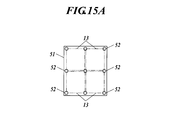
- FIG. 15A is a plan view of a pressing member using pins corresponding to a plurality of semiconductor chips. FIG.
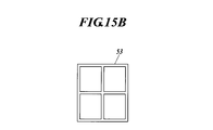
- 15B is a plan view of a pressing member using a frame structure corresponding to a plurality of semiconductor chips. It is explanatory drawing of the press member which presses with one pin. It is sectional drawing of the dicing die bonding film and semiconductor chip which show the generation
- FIGS. 1 to 8B A method of manufacturing a semiconductor device according to an embodiment of the present invention will be described based on FIGS. 1 to 8B.
- a dicing / die bonding film as a wafer processing tape is bonded to the back surface of the semiconductor wafer (the surface opposite to the integrated circuit formation surface), dicing is performed, and then the semiconductor chips are individually picked up. These steps are mainly described.
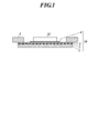
- FIG. 1 is a view showing how a semiconductor wafer and a ring frame for dicing are bonded to a dicing / die bonding film.
- This dicing / die bonding film 10 is provided with an intermediate resin layer 2 on a base film 1, an adhesive layer 3 on top of that, and an adhesive layer 4 on top of that, and in the case of dicing, The semiconductor wafer 11 is attached onto the adhesive layer 4.
- each structure of the dicing die bonding film 10 is illustrated with a thickness larger than the actual thickness for the convenience of description.
- the base film plastics, rubbers, etc. known as a dicing / die bonding film can be used.
- a thermoplastic plastic film is used as the base film.
- the thickness of the substrate film is usually 30 to 300 ⁇ m in view of strength and elongation characteristics and radiation permeability.
- the intermediate resin layer 2 is not particularly limited as long as it is harder than the pressure-sensitive adhesive layer 3. In order to suppress chipping / chipping (chipping) during dicing, the intermediate resin layer 2 having a proper elastic modulus is used.
- the intermediate resin layer 2 is provided by applying a mixture containing an adhesive component and a curing component on a substrate film and then curing it.
- the adhesive component various general-purpose adhesives such as acrylics, polyesters, urethanes, silicones and natural rubbers can be used.
- the curing agent is a compound selected from polyisocyanates, melamine / formaldehyde resins, and epoxy resins, and can be used alone or in combination of two or more.
- the intermediate resin layer 2 may be cured and shrunk by radiation curing after dicing to improve the pick-up property of the chip.
- the thickness of the intermediate resin layer 2 is preferably at least 5 ⁇ m, more preferably 10 ⁇ m or more.
- the pressure-sensitive adhesive layer 3 is not particularly limited as long as it has such a holding property that a defect such as chip fly with the adhesive layer 4 does not occur at dicing, or has a property of facilitating peeling with the adhesive layer 4 at pick-up. good.
- the pressure-sensitive adhesive layer 3 is preferably radiation curable, and in particular, in a dicing / die bonding film, it is preferable that the pressure sensitive adhesive layer 3 be a material that easily peels off the adhesive layer 4.
- the adhesive layer 3 for example, an iodine value of 0..
- An acrylic adhesive comprising a compound having a radiation-curable carbon-carbon double bond of 5 to 20 and a compound selected from polyisocyanates, melamine / formaldehyde resins, and epoxy resins can be used.
- the pressure-sensitive adhesive layer 3 may be formed by coating the pressure-sensitive adhesive on the intermediate resin layer formed on the base film as in the case of a normal dicing tape, and the intermediate resin layer is coated when the pressure-sensitive adhesive is applied. It may be after processing, but if the intermediate resin layer is one whose storage elastic modulus is adjusted by radiation irradiation, it is necessary to coat the intermediate resin layer after it is cured by radiation.
- the adhesive layer 4 separates from the adhesive layer 3 and adheres to the chip when picking up the chip after the semiconductor wafer or the like is bonded and diced, and the chip is fixed to the substrate or lead frame. It is used as an adhesive.
- the adhesive layer 4 is not particularly limited as long as it is a film-like adhesive generally used for dicing / die bonding films, and, for example, known polyimide resins and polyamides used for adhesives Resin, polyether imide resin, polyamide imide resin, polyester resin, polyester imide resin, phenoxy resin, polysulfone resin, polyether sulfone resin, polyphenylene sulfide resin, polyether ketone resin, chlorinated polypropylene resin, acrylic resin, polyurethane resin, epoxy Resins, polyacrylamide resins, melamine resins, etc.
- a silane coupling agent or a titanium coupling agent as an additive to the above-mentioned material or the mixture thereof in order to enhance the adhesion to a chip or a lead frame.
- a chelate modified epoxy resin may be used as a part or all of the epoxy resin. The thickness may be set appropriately, but is preferably about 5 to 100 ⁇ m.
- FIG. 2 is an explanatory view showing a dicing process.
- the dicing die bonding film 10 is attached in advance to the back surface (surface opposite to the integrated circuit forming surface) of the semiconductor wafer 11. Further, the outer periphery of the dicing die bonding film 10 is fixed by the ring frame 5 to prevent the bending of the dicing die bonding film 10. Then, with the back surface of the dicing die bonding film 10 (the opposite side of the semiconductor chip 13) adsorbed to the upper surface of the suction table 14, the upper surface of the semiconductor wafer 11 is diced by the dicing blade 12 and arranged in a grid.
- the semiconductor chip 13 is divided into a plurality of rectangular semiconductor chips 13.
- the dicing / die bonding film 10 is cut by about a half in its thickness direction, and holds the arrayed state of the divided semiconductor chips 13.
- FIG. 2 for convenience of explanation, each configuration of the dicing die bonding film 10 and the semiconductor chip 13 are illustrated with a thickness larger than the actual thickness. Also, the number of semiconductor chips 13 is smaller than the actual number, and is simplified.
- Each semiconductor chip 13 on the dicing die bonding film 10 is individually pressed from the back side through the dicing die bonding film 10 before pickup is performed.
- the pressing operation of each semiconductor chip 13 is performed by the pickup device 20 of the semiconductor chip 13.
- FIG. 4 is a partial cross-sectional view showing the main part of the pickup device 20.
- an infinite number of suction ports 21a are formed on the upper surface, a suction table 21 for suctioning the mounted dicing die bonding film 10, and vacuum suction is performed just below the suction table 21.
- a vacuum chamber (not shown) for suctioning downward from the head, a head 22 that can be moved to any position on a horizontal surface within the vacuum chamber, and the head 22 are mounted, pressing the dicing die bonding film 10 from below
- the first and second pressing members 25 and 26 having the pins 23 and 24 and the suction collet 27 for suctioning the semiconductor chips 13 from above and picking up the semiconductor chips 13 are provided.
- the suction table 21 is provided at the upper part of the vacuum chamber in a state of being directed horizontally, and suction is performed downward from the countless suction ports 21 a formed in the suction table 21 by evacuating the inside of the vacuum chamber.
- the suction and holding of the dicing / die bonding film 10 placed on the upper surface of the suction table 21 is enabled.
- the dicing / die bonding film 10 is mounted on the upper surface of the suction table 21 with the bonding surface of the semiconductor chip 13 facing upward and the back side downward.
- the suction collet 27 is mounted on a head (not shown) which can be positioned at an arbitrary position on the horizontal surface above the suction table 21 so as to move up and down, and is moved up and down by an actuator.
- the suction collet 27 is connected to a negative pressure source, suctions the suction port at the lower end (not shown) onto the upper surface of the semiconductor chip 13 and pulls it upward to peel the semiconductor chip 13 from the dicing die bonding film 10 and pick up I do.
- the first pressing member 25 is positioned at the same position as the suction collet 27 by the head 22 which can be arbitrarily moved by the X-axis and Y-axis servomotors, and is raised by an actuator (not shown) and passes through the dicing die bonding film 10.
- the semiconductor chip 13 is pressed from below to urge peeling of the semiconductor chip 13.
- FIG. 5 is a plan view showing the arrangement of the first pressing member 25 as viewed from above the pin 23. As illustrated, the first pressing member 25 is provided with 20 pins 23 that abut within a range on the inner side than the outer edge of the semiconductor chip 13 (FIG.
- the semiconductor chip 13 to be a target of is pressed from below through the dicing die bonding film 10. Since the entire dicing / die bonding film 10 is adsorbed on the suction table 21, when only one semiconductor chip 13 is pressed from below, the peripheral portion of the semiconductor chip 13 in the dicing / die bonding film 10 is tensioned downward. Therefore, peeling is gradually promoted, and easy and smooth peeling is realized.
- Each pressing member 25, 26 presses the back side of the dicing die bonding film using the pins 23, 24, but in this case, the innumerable suction ports 21 a formed in the suction table 21 are used.
- the pins 23 and 24 are inserted into the respective suction ports 21a to press the dicing die bonding film 10 on the upper side thereof. Further, in FIG. 4, the number of each suction port 21a is small, and in fact, more suction ports 21a are formed with respect to the width of the semiconductor chip 13. Therefore, even in the case of pressing an arbitrary position of the dicing die bonding film 10, it is possible to use an appropriate suction port 21a.
- the second pressing member 26 does not operate simultaneously with the adsorption collet 27, and is performed prior to the pickup of the semiconductor chip 13 to inhibit the peeling of the semiconductor chip 13 It is for removing the dust of time.
- the second pressing member 26 is positioned directly below the target semiconductor chip 13 by the head 22 and presses the semiconductor chip 13 from below with the dicing die bonding film 10 upward by an actuator (not shown).
- the second pressing member 26 also holds the four pins 24 directed upward, and presses the target semiconductor chip 13 from a lower position in a predetermined position.
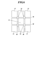
- FIG. 6 is a plan view showing the position where four pins 24 press the rectangular semiconductor chip 13 to be pressed.
- each pin 24 is arranged to press the position of the four intersections of the dicing grooves M surrounding the periphery of the semiconductor chip 13 to be pressed from below.
- FIG. 7 is an operation explanatory view showing a state where the pressing member 22 is raised, and each pin 24 enables pressing of the dicing die bonding film 10 on the upper surface of the table through the suction port 21a of the suction table 21.
- FIG. 8A is an enlarged cross-sectional view showing a state before pressing of the semiconductor chip 13 through the pins 24 by the second pressing member 26, and FIG. 8B is an enlarged cross-sectional view showing a state after pressing of the semiconductor chip 13.
- dust D is generated from each layer of the dicing die bonding film 10 by cutting and adheres in the grooves.
- dust D in the adhesive layer 3 (and further, the adhesive layer 2) inhibits the pickup of the semiconductor chip 13 when it adheres across the adhesive layer 2 and the adhesive layer 3 in the groove. Therefore, before performing the pickup, four pins 24 are provided at four vertex positions of dicing grooves around the target semiconductor chip 13, in this embodiment, dicing grooves M which become four sides surrounding the rectangular semiconductor chip 13.
- the second pressing member 26 is positioned so that the center position of each of the circular pins 24 and the center position of each of the intersections of the dicing grooves M coincide with each other.
- the dimensions of each part are as follows: one side of the semiconductor chip 13 is 10 to 16 mm, the diameter of the pin 24 is 200 to 350 ⁇ m, the width of the dicing groove is 50 ⁇ m, and dicing by each pin 24 The amount of push-up of the die bonding film 10 is about 10 ⁇ m.
- the dust D adhering can be shaken off, or the dust D which straddled the adhesion layer 2 and the adhesive bond layer 3 can be parted.
- the first pressing member 25 and the second pressing member 26 use actuators of the same specifications as a drive source for the vertical movement, the moving speed of pressing of each pin 24 is the same as that of the semiconductor chip. There is no difference from the rising speed when the pin 23 presses the back side of the dicing die bonding film during peeling.
- the pressure for removing the dust D may press the entire periphery of the semiconductor chip 13 along the dicing groove M, or may be partially pressed like the pressing member 26.
- the second pressing member 26 presses the intersection of the dicing groove M in the lateral direction and the dicing groove M in the longitudinal direction, but generation and adhesion of dust D easily occur at the intersection of the dicing groove M, and such a point The adhesion removal can be performed more effectively by pressing the.
- the outer diameter of each pin 24 of the second pressing member 26 is larger than the width of the dicing groove M, and when pressed, the outer edge of the semiconductor chip 13 is also pressed. The outer edge portion of the semiconductor chip 13 may be pressed together with the groove M. Further, only the dicing groove M may be pressed with a narrow width so as not to overlap the semiconductor chip 13.
- the head 22 positions the first pressing member 25 on the same semiconductor chip 13, and at the same time the suction collet 27 on the same semiconductor chip 13. And position the adsorption collet 27 downward to adsorb the semiconductor chip 13. Then, the suction collet 27 is lifted, and at the same time, the first pressing member 25 is lifted to press the semiconductor chip 13 from below.
- the dust D in the dicing groove M is removed or separated from the state of straddling the boundary between the adhesive layer 4 and the adhesive layer 3 by the pressing by the second pressing member 26 described above, so the semiconductor chip 13 has a peeling boundary line
- the semiconductor chip 13 is well picked up from the interface between the adhesive layer 3 and the adhesive layer 4 which is K (see FIG.
- the semiconductor chip 13 is picked up by the adsorption collet 27.
- the invention is not limited thereto, for example, all semiconductor chips After the pressing by the second pressing member 25 for dust removal is completed in advance, the pickup of each semiconductor chip 13 may be performed.
- the method of pickup is not limited to the method of picking up from above while pressing the central portion of the semiconductor chip 13 by the pins 23 of the first pressing means 25 as described above.
- a suction head 31 which holds the semiconductor chip 13 to which the expand ring 8 is attached and the dicing die bonding film 10 and which can be moved and positioned arbitrarily along the horizontal plane below it.
- a pickup collet not shown, may be used above the semiconductor chip 13.
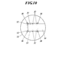
- FIG. 10 is a plan view of the suction head 31, and FIG. 11 is a cross-sectional view of the suction head 31 along the vertical plane.
- the inside of the suction head 31 of the pickup device 30 is evacuated and six suction ports 32 are formed on the upper surface thereof.
- a recess 33 is formed on the upper surface of the suction head 31, and a movable cover 34 is provided which fits in the recess 33 and slides along the upper surface of the head to open and close the recess 33.
- the recess 32 and the movable lid 34 are set to be somewhat narrower than the semiconductor chip 13.
- Each suction port 32 is disposed along the outer edge of the recess 33 so as to be substantially inside the recess 33.
- the suction collet and the suction head 31 are directly below the semiconductor chip 13 with the movable cover 34 closed.
- the suction collet and the suction head 31 perform suction at the top and bottom.
- the suction ports 32 are slightly opened, and the back surface of the dicing die bonding film 10 is adsorbed on the upper surface of the suction head 31.
- the movable cover 34 is gradually slid, as shown in FIG. 12, the recess 33 is gradually opened, and the internal space of the recess 33 is decompressed by the suction port 32.
- a pressing member 35 having the same structure as that of the second pressing member 24 described above is provided.
- the pressing member 35 also has four pins 36 for pressing four intersecting positions in the dicing groove M around the semiconductor chip 13, and has a structure in which vertical movement is given by the actuator 37.
- through holes 38 are formed on the upper surface of the suction head 31 at positions corresponding to four corner portions with respect to the semiconductor chip 13.
- Each pin 36 can be made to project. That is, after the back surface of the dicing die bonding film 10 is adsorbed on the upper surface of the adsorption head 31, the pressing member 35 is raised before the movable lid 34 is opened, and the four corners of the semiconductor chip 13 are pressed from below by the pins 36 Do.
- the dust D in the dicing groove M is removed or separated from the state in which the two layers 3 and 4 are straddled.
- the movable lid 34 is opened to peel off the adhesive layer 3 and the adhesive layer 4 of the dicing / die bonding film 10 with respect to the semiconductor chip 13.
- the suction collet picks up the semiconductor chip 13 and thereafter the same steps as described above are performed.
- Embodiments [2] Another embodiment is shown about the method of pickup.
- a suction head which holds the semiconductor chip 13 and the dicing die bonding film 10 to which the expand ring 8 is mounted, and which can be moved and positioned arbitrarily along the horizontal plane below it.
- the pickup D and the dust D may be removed using a pickup device 40 provided with an adsorption collet (not shown) provided above the semiconductor chip 13.
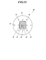
- FIG. 13 is a plan view of the suction head 41
- FIG. 14 is a cross-sectional view of the suction head 41 along the vertical plane.
- the inside of the suction head 41 of the pickup device 40 is evacuated and a plurality of suction ports 42 are formed on the upper surface thereof.
- the suction head 41 is provided with rectangular projecting blocks 43, 44 and 45 so as to be concentric with the upper surface center thereof.
- the central projecting block 43 has a square pole shape
- the outer projecting block 44 is formed in a rectangular frame shape so as to surround the periphery of the projecting block 43, and the outer projecting block 45 further protrudes the projecting block 44 It is formed in the shape of a square frame so as to surround it.
- the protruding block 45 is set to substantially the same size as the semiconductor chip 13 to be picked up. These three projecting blocks 43, 44, 45 simultaneously start projecting upward with their upper end faces aligned, and the outermost projecting block 45 stops rising by a certain amount of projection and further rises Then, the second protruding block 44 is stopped at a fixed amount of protruding, and the central protruding block 43 is stopped in the most protruding state. As a result, in the projecting state, the projecting blocks 43 to 45 can project in a substantially pyramid shape with the central portion projecting most as shown by a two-dot chain line in FIG.
- the three blocks 43 to 45 may be equipped with three actuators that move up and down for each block if they operate in the above-mentioned order, and interlocked structures are provided between the blocks so as to interlock mechanically. It is good.
- the suction head 41 is provided with a pressing member 46 for processing the dust D in the same manner as the pressing members 24 and 35 described above.
- the pressing member 46 is a rectangular frame for pressing the entire rectangular range of the dicing groove M surrounding the periphery of the semiconductor chip 13 and has a structure in which vertical movement is given by an actuator (not shown).
- the rectangular frame-shaped pressing member 46 has the above-described projecting blocks 43 to 45 and is disposed on the suction head 41 so as to surround the blocks 43 to 45. That is, after the inside of the head 41 is in a vacuum state and the back surface of the dicing die bonding film 10 is adsorbed on the upper surface of the suction head 41, only the pressing member 46 is raised before starting the raising operation of each projecting block 43-45.
- the pressing members 24, 35, and 46 for processing the dicing dust D are illustrated as being mounted on the pickup device, but the present invention is not limited thereto. That is, after separately providing a dedicated processing device for processing dust D separately from the pickup device and processing the dust D by the processing device, the dicing die bonding film 10 and the semiconductor chip are used in the pickup device. 13 may be transported to perform a pickup operation.
- the pressing members 24, 35, and 46 described above each process the dust D for one semiconductor chip 13, as in the example of the pressing member 51 shown in the plan view of FIG. It is good also as composition provided with pin 52 which can press an intersection position of a dicing slot of the circumference simultaneously about semiconductor chip 13 (here four are illustrated). Further, as in the example of the pressing member 53 shown in the plan view of FIG. 15B, the entire dicing grooves around the plurality of adjacent semiconductor chips 13 (here, four are illustrated) can be formed into a frame shape that can be pressed simultaneously. It is good also as composition.
- the pressing member for performing the dust processing is configured by one pin, and the pressing position is moved along the dicing grooves around the target semiconductor chip 13 as in the example shown in FIG. It may be pressed by tracing.
- Epoxy-based adhesive layer (1) 50 parts by mass of cresol novolac type epoxy resin (epoxy equivalent 197, molecular weight 1200, softening point 70 ° C.) as an epoxy resin, 1.5 parts by mass of ⁇ -mercaptopropyltrimethoxysilane as a silane coupling agent, ⁇ -ureidopropyltriethoxysilane Cyclohexanone was added to a composition consisting of 3 parts by mass and 30 parts by mass of silica filler having an average particle diameter of 16 nm, and the mixture was stirred and mixed, and was further kneaded using a bead mill for 90 minutes.
- cresol novolac type epoxy resin epoxy equivalent 197, molecular weight 1200, softening point 70 ° C.
- EP-49-23 (trade name of ADEKA Co., Ltd., a chelate-modified bisphenol F-type epoxy resin, epoxy equivalent weight 175 g / eq) as an epoxy resin
- Mirex XLC-LL (a product of Mitsui Chemicals, Inc.) as a phenolic resin Name, hydroxyl group equivalent 175 g / eq, water absorption 1.8%, heating weight reduction at 350 ° C 4%) 50 parts by mass
- Cuasol 2PZ as a curing accelerator (trade name of Shikoku Kasei Co., Ltd., 2-phenylimidazole)
- An adhesive composition comprising 0.4 parts by mass, 200 parts by mass of an acrylic resin, 200 parts by mass of SG-708-6 (trade name of Nagase ChemteX Co., Ltd., weight average molecular weight 700,000, glass transition temperature 6 ° C.) The mixture was stirred and mixed to prepare an adhesive varnish.
- a photopolymerization initiator 0.5 parts by mass of Irgacure 184 and 150 parts by mass of ethyl acetate as a solvent were added to the compound (A) solution and mixed to obtain a radiation-curable pressure-sensitive adhesive composition.
- Intermediate resin layer (1) 100 parts by mass of acrylic resin (mass average molecular weight: 600,000, glass transition temperature -20 ° C.), 10 parts by mass of polyisocyanate compound (made by Nippon Polyurethane Industry Co., Ltd., trade name: Coronate L) as a curing agent, and intermediate resin The layer composition was obtained.
- the intermediate resin layer composition is coated on a 100 ⁇ m thick ethylene-vinyl acetate copolymer film as a base film so that the dry film thickness is 10 ⁇ m, dried at 110 ° C. for 3 minutes, and further an adhesive layer
- the composition was applied to a dry film thickness of 10 ⁇ m and dried at 110 ° C. for 3 minutes to prepare a pressure-sensitive adhesive tape.
- the adhesive layer composition was directly coated on the substrate film and dried in the case where there was no intermediate resin layer.
- An adhesive film was pasted on the adhesive layer of the adhesive tape to obtain dicing die bonding films according to Examples 1 to 5 and Comparative Examples 1 to 5 shown in Table 1.
- the present invention may be used in the field of manufacturing semiconductor devices using a wafer processing tape.
Landscapes
- Dicing (AREA)
- Container, Conveyance, Adherence, Positioning, Of Wafer (AREA)
- Die Bonding (AREA)
Abstract
Description
上記粘着テープは、半導体ウエハをダイシングする工程で切断されたチップが飛び散らないようにウエハを固定するためのものであるため、ウエハを固定する高い粘着力を有するものであるが、個々のチップをピックアップする工程では、この粘着テープから接着剤層が付着したチップを剥離させなければならない。
そこで、従来は、ウエハ加工用テープをウエハの径方向と周方向に引き伸ばした状態でウエハの周囲をエキスパンドリングで保持し、かかる状態でピックアップしたいチップについて、粘着テープの背面を吸着ステージにより吸着させながら昇降可能なピンにより突き上げて、粘着テープと接着剤層との間で剥離させてピックアップを行っていた(例えば、特許文献1参照)。
また、粘着テープの背面を吸着駒の上面により吸着し、吸着駒の上面から突出可能であり、同心円上に配置された複数の突き上げブロックでピックアップ対象のチップのみを押し上げて支承すると共に当該チップを上方から吸着コレットで上方に吸引し、最終的に中心の突き上げブロックが最も突出した状態となるように内側のブロックを徐々に上昇させることでウエハ加工用テープの剥離を行っていた(例えば、特許文献2参照)。
特許文献2に記載のピックアップ方式は、特許文献1のピックアップ方式によるピックアップ不良を改善したものであるが、ウエハ加工用テープTの接着剤層T3は、チップW1の多段層化の要求に応じて軟化する傾向にあり、その結果、ウエハをダイシングする工程で接着剤層T3のダストDが周囲に飛散しやすくなり、ピックアップの成功率が低下するという問題が生じていた。
(1)半導体ウエハにウエハ加工用テープを貼り付けた後、前記半導体ウエハをダイシングして複数の半導体チップに分割する工程と、前記ウエハ加工用テープに貼り付けられた前記複数の半導体チップのうち、剥離の対象となる半導体チップを前記ウエハ加工用テープからピックアップする工程とを備え、ダイシング溝の剥離対象となる前記半導体チップを囲む領域についてその全体また一部分を前記ウエハ加工用テープの背面側から押圧した後に前記半導体チップを前記ウエハ加工用テープからピックアップことを特徴とする半導体装置の製造方法、
(2)前記ダイシング溝の半導体チップを囲む領域の押圧を、当該領域に沿った形状の枠により行うことを特徴とする請求項1記載の半導体装置の製造方法、
(3)前記ダイシング溝の半導体チップを囲む領域の押圧を、当該領域に沿って配置された複数のピンにより行うことを特徴とする請求項1記載の半導体装置の製造方法、
(4)前記前記ダイシング溝の半導体チップを囲む領域の押圧を、複数個の半導体チップ単位で行うことを特徴とする請求項1から3のいずれか一項に記載の半導体装置の製造方法、
により、本願発明の課題の解決を図るものである。
なお、上記「ダイシング溝の剥離対象となる前記半導体チップを囲む領域」とは、ダイシング溝に囲まれた領域の意味ではなく、ウエハ全体のダイシング溝全体の内、剥離対象の半導体チップを囲んでいるダイシング溝の一部分を示している。
本発明の実施形態たる半導体装置の製造方法について図1から図8Bに基づいて説明する。
この実施形態では、半導体ウエハの裏面(集積回路形成面の反対側の面)にウエハ加工用テープとしてのダイシング・ダイボンディングフィルムを貼合してダイシング行い、その後、半導体チップを個々にピックアップする工程に特徴を有するものであり、かかる工程について主に説明を行うものとする。
半導体装置の製造方法の説明を行う前に、まず、ダイシング・ダイボンディングフィルム10の構成について説明を行う。図1は、ダイシング・ダイボンディングフィルムに半導体ウエハとダイシング用リングフレームが貼合された様子を示す図である。
このダイシング・ダイボンディングフィルム10は基材フィルム1の上に中間樹脂層2、その上に粘着剤層3、その上に接着剤層4が積層して設けられており、ダイシングの際には、接着剤層4の上に半導体ウエハ11が取り付けられる。なお、図1ではダイシング・ダイボンディングフィルム10の各構成について説明の便宜のために実際よりも厚みをもって図示している。
また、放射線透過性であることが好ましく、特に粘着剤層に放射線硬化性の粘着剤を使用する場合にはその粘着剤が硬化する波長での放射線透過性の良いものを選択する必要がある。基材フィルムの厚みは、強伸度特性、放射線透過性の観点から通常30~300μmが適当である。
さらに、中間樹脂層2に放射線硬化性を持たせることで、ダイシング後に放射線硬化により中間樹脂層2を硬化収縮させチップのピックアップ性を向上させても良い。
中間樹脂層2の厚さは少なくとも5μm、より好ましくは10μm以上であることが好ましい。
粘着剤層3の形成は、通常のダイシングテープ同様に基材フィルムに形成された中間樹脂層上に粘着剤を塗工して製造してよく、粘着剤の塗工は、中間樹脂層が塗工された後であればよいが、中間樹脂層が放射線照射によって貯蔵弾性率が調整されるものであれば、中間樹脂層が放射線によって硬化された後に塗工することが必要である。
以下、半導体装置の製造方法について順を追って説明する。
まず、単結晶シリコンからなる半導体ウエハ11の主面に周知の製造プロセスに従って集積回路を形成した後、半導体ウエハ11の裏面をグラインダで研削し、ダメージ層を、エッチングによって除去し、例えば20μm~50μm程度まで薄くする。
図2はダイシング工程を示す説明図である。ダイシングの際には、予め半導体ウエハ11の背面(集積回路形成面の反対側の面)にダイシング・ダイボンディングフィルム10を貼り付ける。また、ダイシング・ダイボンディングフィルム10の外周はリングフレーム5で固定し、ダイシング・ダイボンディングフィルム10の撓みを防止する。
そして、ダイシング・ダイボンディングフィルム10の背面(半導体チップ13の逆側)を吸着テーブル14の上面に吸着させた状態で、ダイシングブレード12により半導体ウエハ11の上面をダイシングして、格子状に配列された複数の矩形の半導体チップ13に分割する。このとき、ダイシング・ダイボンディングフィルム10は、その厚さ方向の半分程度だけ切断を行い、分割されたそれぞれの半導体チップ13の配列状態を保持する。
なお、図2ではダイシング・ダイボンディングフィルム10の各構成及び半導体チップ13を説明の便宜上実際よりも厚みをもって図示している。また、半導体チップ13の個体数も実際より少なく図示し、簡略化している。
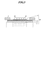
中間樹脂層2又は粘着剤層3に放射線硬化性のものを使用している場合には、図3に示すように、ダイシング・ダイボンディングフィルム10の背面側から放射線照射を行う。
これにより、中間樹脂層2の硬化又は粘着剤層3の粘着性の低下を図り、半導体チップ13の剥離性を高める。
次に、ダイシング・ダイボンディングフィルム10の背面側からリングフレーム5の内側に入り込むようにエキスパンドリング8(図9参照)が装着される。これにより、ダイシング・ダイボンディングフィルム10はウエハ装着位置を中心として放射線方向に張力を受けて水平方向に弛みなく引き伸ばされる。
ダイシング・ダイボンディングフィルム10上の各半導体チップ13は、ピックアップが行われる前にその背面側からダイシング・ダイボンディングフィルム10を介して個々に押圧作業が行われる。
この各半導体チップ13の押圧作業は、半導体チップ13のピックアップ装置20によって実行される。
なお、各押圧部材25,26はいずれもピン23,24を利用してダイシング・ダイボンディングフィルムの背面側を押圧するが、その際には、吸着テーブル21に形成された無数の吸着口21aを利用し、当該各吸着口21aに各ピン23,24を挿通させてその上側のダイシング・ダイボンディングフィルム10を押圧している。また、図4では各吸着口21aは少なく図示しており、実際には、半導体チップ13の幅に対してより多くの吸着口21aが形成されている。従って、ダイシング・ダイボンディングフィルム10の任意の位置を押圧する場合でもあっても適切な吸着口21aを利用することができる。
かかる第二の押圧部材26は、ヘッド22により目標とする半導体チップ13の真下に位置決めされ、図示しないアクチュエータにより上方してダイシング・ダイボンディングフィルム10を介して半導体チップ13を下方から押圧する。
この第二の押圧部材26も、上方を向いた四本のピン24を保持しており、目標の半導体チップ13に対して下方から所定位置の押圧を行う。図6は四本のピン24が押圧対象の矩形半導体チップ13を押圧する位置を示す平面図である。図示のように、各ピン24は押圧対象の半導体チップ13に対して、その周囲を取り囲むダイシング溝Mの四つの交点の位置を下方から押圧する配置となっている。また、図7は押圧部材22を上昇させた状態を示す動作説明図であり、各ピン24は吸引テーブル21の吸引口21aを通じてテーブル上面のダイシング・ダイボンディングフィルム10の押圧を可能としている。
ダイシング溝Mには、切削によりダイシング・ダイボンディングフィルム10の各層からダストDを生じ溝内に付着する。その中でも接着剤層3(さらには粘着剤層2)におけるダストDは、溝内で粘着層2と接着剤層3とにまたがって付着した場合に、半導体チップ13のピックアップを阻害する。
そこで、ピックアップを実行する前に、対象となる半導体チップ13の周囲のダイシング溝、この実施形態では、矩形の半導体チップ13を囲む四辺となるダイシング溝Mの四つの頂点位置に四つのピン24を押し当てることでダストDに押圧の衝撃を付与或いは押圧による振動を付与している。
なお、円棒状の各ピン24の中心位置とダイシング溝Mの各交点の中心位置とが一致するように第二の押圧部材26の位置決めが行われる。
また、各部の寸法を例示すると、半導体チップ13の一辺は10~16[mm]、ピン24の直径は200~350[μm]、ダイシング溝の幅は50[μm]、各ピン24によるダイシング・ダイボンディングフィルム10の押し上げ量は10[μm]程度である。
なお、第一の押圧部材25と第二の押圧部材26とは、その上下動の駆動源として同じ仕様のアクチュエータを使用しているため、各ピン24の押し当ての移動速度は、半導体チップの剥離の際にピン23がダイシング・ダイボンディングフィルムの背面側を押圧する際の上昇速度と変わらない。
また、第二の押圧部材26の各ピン24は、その外径がダイシング溝Mの幅よりも大きく、押圧時には半導体チップ13の外縁部も含めて押圧することとなるが、このように、ダイシング溝Mと共に半導体チップ13の外縁部を含めて押圧しても良い。また、半導体チップ13に重ならないよう、狭い幅でダイシング溝Mのみを押圧しても良い。
なお、ここでは、一つの半導体チップ13についてダスト除去のための第二の押圧部材25による押圧とピックアップとを連続して行う動作例を例示したが、これに限らず、例えば、全ての半導体チップに13について先にダスト除去のための第二の押圧部材25による押圧を完了させてから、各半導体チップ13のピックアップを実行しても良い。
ピックアップされた半導体チップ13は、基板実装工程に搬送され、接着剤などを介して配線基板上に実装され、Auワイヤを介して配線基板の電極と電気的に接続される。
そして、半導体チップが実装され配線基板はモールド樹脂で封止され、パッケージ化されて製造の工程が終了する。
以上のように、上述した半導体装置の製造方法では、ピックアップ工程において、ダイシング・ダイボンディングフィルム10から半導体チップを剥離するピックアップ工程の前に、当該半導体チップ13の周囲のダイシング溝Mの四つの頂点位置を下方から押圧することで、ダイシング溝M内の各部に付着したダストDが除去され、或いは接着剤層4と粘着剤層3にまたがった状態のダストDが分離され、その結果、接着剤層4と粘着剤層3の境界で導体チップ13が剥離する際にダストDによる阻害が抑止され、ピックアップ作業の成功率が向上する。
ピックアップの方法は、上述のように、第一の押圧手段25の各ピン23により半導体チップ13の中央部を押圧しつつ上方からピックアップを行う方法に限られるものではない。
例えば、図9に示すように、エキスパンドリング8が装着された半導体チップ13及びダイシング・ダイボンディングフィルム10を保持し、その下方において、水平面に沿って任意に移動位置決め可能且つ昇降可能な吸着ヘッド31を備え、半導体チップ13の上方には図示しない吸着コレットを備えるピックアップ装置30を使用しても良い。
ピックアップ装置30の吸着ヘッド31は内部が真空引きされると共にその上面に吸引口32が六つ形成されている。
さらに、吸着ヘッド31の上面には凹部33が形成されると共に当該凹部33に嵌合すると共にヘッド上面に沿ってスライド移動することで凹部33を開閉する可動蓋34とを備えている。
図10においてピックアップ対象となる半導体チップ13に対して吸着ヘッド31を適正に位置決めした場合における半導体チップ13の位置を二点差線で示す。図示のように、凹部32及び可動蓋34は半導体チップ13よりも幾分幅が狭く設定されている。そして、各吸引口32は、凹部33の外縁部に沿って当該凹部33のほぼ内側となるように配置されている。
即ち、吸着ヘッド31の上面にダイシング・ダイボンディングフィルム10の背面を吸着させてから可動蓋34を開く前に、押圧部材35を上昇させ、各ピン36により半導体チップ13の四隅近傍を下方から押圧する。これにより、ダイシング溝M内のダストDを除去又は二層3,4をまたがっている状態から分離させる。
そして、可動蓋34を開くことで半導体チップ13に対してダイシング・ダイボンディングフィルム10の粘着剤層3と接着剤層4との剥離を行う。その後、吸着コレットが半導体チップ13をピックアップして、それ以降は前述と同じ工程が実行される。
ピックアップの方法について、さらに他の実施形態を示す。
前述した図9の例のように、エキスパンドリング8が装着された半導体チップ13及びダイシング・ダイボンディングフィルム10を保持し、その下方において、水平面に沿って任意に移動位置決め可能且つ昇降可能な吸着ヘッド41を備え、半導体チップ13の上方には図示しない吸着コレットを備えるピックアップ装置40を使用してピックアップ及びダストDの除去を行っても良い。
ピックアップ装置40の吸着ヘッド41は内部が真空引きされると共にその上面に吸引口42が複数形成されている。
さらに、吸着ヘッド41は、その上面中央に同心となるように矩形状の突出ブロック43,44,45が設けられている。中心の突出ブロック43は、四角柱状であり、その外側の突出ブロック44は、突出ブロック43の周囲を囲むように四角い枠状に形成されており、さらにその外側の突出ブロック45は突出ブロック44を囲むように四角い枠状に形成されている。そして、突出ブロック45は、ピックアップの対象となる半導体チップ13とほぼ同じ大きさに設定されている。
これら三つの突出ブロック43,44,45は、それぞれの上端面を揃えた状態で同時に上方に突出を開始し、ある一定の突出量で一番外側の突出ブロック45が上昇を停止し、さらに上昇して一定の突出量で二番目の突出ブロック44が停止し、中心の突出ブロック43が最も突出した状態で停止する。その結果、突出ブロック43~45は、突出状態において、図14の二点差線に示すように、中央部が最も突出した略ピラミッド状となって突出することが可能となっている。かかる状態で順番に突出動作を行うことにより、半導体チップ13からダイシング・ダイボンディングフィルム10(正確には、ダイシング・ダイボンディングフィルム10の粘着剤層3と接着剤層4)を剥離させる際に、半導体チップ13の外側から順番に剥離させることができ、徐々に剥離を促すため、半導体チップの保護を図ることが可能となる。
なお、三つのブロック43~45は、上記順番で動作するのであれば各ブロックごとに上下動させる三つのアクチュエータを装備しても良いし、機械的に連動するよう各ブロック間に連動構造を施しても良い。
この矩形枠状の押圧部材46は、その内側に前述した突出ブロック43~45を擁し、これらのブロック43~45を囲むように吸着ヘッド41に配置されている。
即ち、ヘッド41内を真空状態とし、吸着ヘッド41の上面にダイシング・ダイボンディングフィルム10の背面を吸着させてから各突出ブロック43~45の上昇動作を開始する前に、押圧部材46のみを上昇させ、半導体チップ13の周囲を下方から押圧する。これにより、ダイシング溝M内のダストDを除去又は二層3,4をまたがっている状態から分離させる。
そして、前述した通りに各突出ブロック43~45を上昇させ、半導体チップ13に対してダイシング・ダイボンディングフィルム10の粘着剤層3と接着剤層4との剥離を行う。その後、吸着コレットが半導体チップ13をピックアップして、それ以降は前述と同じ工程が実行される。
なお、上述のように、押圧部材46は各突出ブロック43~45とは別に動作を行うので、これらとは別に独立した駆動源を設ける必要がある。
なお、前述した各実施形態では、ダイシングのダストDの処理を行うための押圧部材24,35,46について、いずれもピックアップ装置に搭載する例を例示したが、これに限るものではない。つまり、ピックアップ装置とは別にダストDの処理を行うための専用の処理装置を独立して設け、当該処理装置でダストDの処理を行ってから、ピックアップ装置にダイシング・ダイボンディングフィルム10及び半導体チップ13を搬送し、ピックアップ動作を行うように構成しても良い。
また、図15Bの平面図に示す押圧部材53の例のように、隣接する複数(ここでは四つを例示)の半導体チップ13について同時にその周囲のダイシング溝の全体を押圧可能な枠状とする構成としても良い。
次に、各種のダイシング・ダイボンディングフィルムを用いて半導体チップのピックアップ及び事前の半導体チップ周囲の押圧を行った場合の各実施例1~5と、各実施形態1~5と条件を等しくしつつ半導体チップ周囲の押圧を行わなかった比較例1~5とについて、ピックアップの成功率の比較試験を行った。
当該比較試験の結果について、以下に説明する。

上記比較試験の適用条件は、上記の表1に示す通りである。
また、表1の接着剤層、粘着剤層、中間樹脂層の種別については以下の通りである。
エポキシ樹脂としてクレゾールノボラック型エポキシ樹脂(エポキシ当量197、分子量1200、軟化点70℃)50質量部、シランカップリング剤としてγ-メルカプトプロピルトリメトキシシラン1.5質量部、γ-ウレイドプロピルトリエトキシシラン3質量部、平均粒径16nmのシリカフィラー30質量部からなる組成物に、シクロヘキサノンを加えて撹拌混合し、更にビーズミルを用いて90分混練した。
これにアクリル樹脂(質量平均分子量:80万、ガラス転移温度-17℃)100質量部、6官能アクリレートモノマーとしてジペンタエリスリトールヘキサアクリレート5部、硬化剤としてヘキサメチレンジイソシアネートのアダクト体0.5部、キュアゾール2PZ(四国化成(株)製、商品名:2-フェニルイミダゾール)2.5部を加え、撹拌混合し、真空脱気し、接着剤を得た。
接着剤を厚さ25μmの離型処理したポリエチレンテレフタレートフィルム上に乾燥後の厚さが表1に示す厚さとなるように塗布し、110℃で1分間加熱乾燥して、接着フィルムを作製した。
エポキシ樹脂としてEP-49-23((株)ADEKA製商品名、キレート変性ビスフェノールF型エポキシ樹脂、エポキシ当量175g/eq)50質量部、フェノール樹脂としてミレックスXLC-LL(三井化学(株)製商品名、水酸基当量175g/eq、吸水率1.8%、350℃における加熱重量減少率4%)50質量部、硬化促進剤としてキュアゾール2PZ(四国化成(株)製商品名、2-フェニルイミダゾール)0.4質量部、アクリル樹脂は、SG-708-6(ナガセケムテックス(株)製商品名、重量平均分子量70万、ガラス転移温度6℃)200質量部からなる接着剤組成物に、メチルエチルケトンを加えて攪拌混合して接着剤ワニスを作製した。作製した接着剤組成物の接着剤ワニスを離型フィルム上に、乾燥後の厚さが20μmになるように塗工し、110℃で3分間乾燥させ、接着フィルムを作製した。
溶媒のトルエン400g中に、n-ブチルアクリレート128g、2-エチルヘキシルアクリレート307g、メチルメタアクリレート67g、メタクリル酸1.5g、重合開始剤としてベンゾイルペルオキシドの混合液を、適宜、滴下量を調整し、反応温度および反応時間を調整し、官能基をもつ化合物(1)の溶液を得た。
次にこのポリマー溶液に、放射線硬化性炭素-炭素二重結合および官能基を有する化合物(2)として、別にメタクリル酸とエチレングリコールから合成した2-ヒドロキシエチルメタクリレート2.5g、重合禁止剤としてハイドロキノンを適宜滴下量を調整して加え反応温度および反応時間を調整して、放射線硬化性炭素-炭素二重結合を有する化合物(A)の溶液を得た。続いて、化合物(A)溶液中の化合物(A)100質量部に対してポリイソシアネート(B)として日本ポリウレタン社製:コロネートLを1質量部を加え、光重合開始剤として日本チバガイギー社製:イルガキュアー184を0.5質量部、溶媒として酢酸エチル150質量部を化合物(A)溶液に加えて混合して、放射線硬化性の粘着剤組成物を得た。
アクリル樹脂(質量平均分子量:60万、ガラス転移温度-20℃)100質量部、硬化剤としてポリイソシアネート化合物(日本ポリウレタン(株)製、商品名:コロネートL)10質量部を混合して中間樹脂層組成物を得た。
そして、比較試験の結果を下記の表2に示す。なお、それぞれのピックアップ方式において、図6に示すように四本のピンで押圧した場合、四角形の枠上のピンで押圧した場合、および1本のピンでチップの周囲をダイシング溝に沿って押圧位置を移動させて押圧した場合のそれぞれについてピックアップ試験を行ったが、全て同じ結果となったため、表2にはまとめて示した。
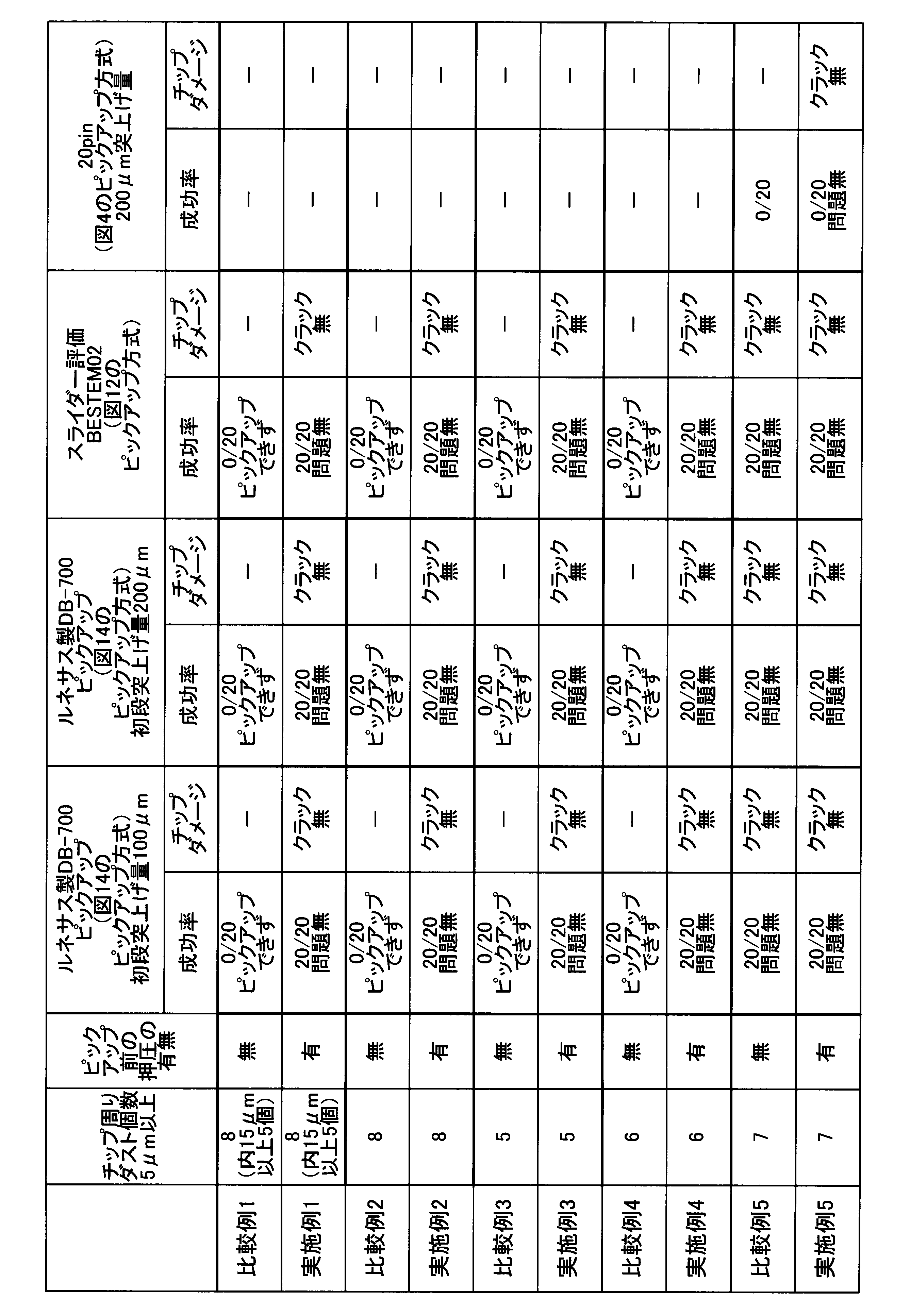
また、実施例5及び比較例5は、図12,14の方式では、いずれも高いピックアップの成功率を得ることができたが、図4の方式では、比較例5はピックアップをおこなうことができなかった。
2 中間樹脂層
3 粘着剤層
4 接着剤層
10 ダイシング・ダイボンディングフィルム(ウエハ加工用テープ)
11 半導体ウエハ
13 半導体チップ
20,30,40 ピックアップ装置
24,52 ピン
26 第二の押圧部材
35,46,51,53 押圧部材
36 ピン
D ダスト
M ダイシング溝
Claims (4)
- 半導体ウエハにウエハ加工用テープを貼り付けた後、前記半導体ウエハをダイシングして複数の半導体チップに分割する工程と、
前記ウエハ加工用テープに貼り付けられた前記複数の半導体チップのうち、剥離の対象となる半導体チップを前記ウエハ加工用テープからピックアップする工程とを備え、
ダイシング溝の剥離の対象となる前記半導体チップを囲む領域についてその全体また一部分を前記ウエハ加工用テープの背面側から押圧した後に前記半導体チップを前記ウエハ加工用テープからピックアップすることを特徴とする半導体装置の製造方法。 - 前記ダイシング溝の半導体チップを囲む領域の押圧を、当該領域に沿った形状の枠により行うことを特徴とする請求項1記載の半導体装置の製造方法。
- 前記ダイシング溝の半導体チップを囲む領域の押圧を、当該領域に沿って配置された複数のピンにより行うことを特徴とする請求項1記載の半導体装置の製造方法。
- 前記前記ダイシング溝の半導体チップを囲む領域の押圧を、複数個の半導体チップ単位で行うことを特徴とする請求項1から3のいずれか一項に記載の半導体装置の製造方法。
Priority Applications (2)
| Application Number | Priority Date | Filing Date | Title |
|---|---|---|---|
| KR1020127025603A KR20130009799A (ko) | 2010-03-31 | 2011-03-23 | 반도체 장치의 제조 방법 |
| CN201180015691.7A CN102822946B (zh) | 2010-03-31 | 2011-03-23 | 半导体装置的制造方法 |
Applications Claiming Priority (2)
| Application Number | Priority Date | Filing Date | Title |
|---|---|---|---|
| JP2010-080509 | 2010-03-31 | ||
| JP2010080509A JP2011216529A (ja) | 2010-03-31 | 2010-03-31 | 半導体装置の製造方法 |
Publications (1)
| Publication Number | Publication Date |
|---|---|
| WO2011125492A1 true WO2011125492A1 (ja) | 2011-10-13 |
Family
ID=44762446
Family Applications (1)
| Application Number | Title | Priority Date | Filing Date |
|---|---|---|---|
| PCT/JP2011/056890 Ceased WO2011125492A1 (ja) | 2010-03-31 | 2011-03-23 | 半導体装置の製造方法 |
Country Status (5)
| Country | Link |
|---|---|
| JP (1) | JP2011216529A (ja) |
| KR (1) | KR20130009799A (ja) |
| CN (1) | CN102822946B (ja) |
| TW (1) | TWI427691B (ja) |
| WO (1) | WO2011125492A1 (ja) |
Cited By (4)
| Publication number | Priority date | Publication date | Assignee | Title |
|---|---|---|---|---|
| CN103311150A (zh) * | 2012-03-14 | 2013-09-18 | 富士电机株式会社 | 半导体制造装置以及半导体制造装置的控制方法 |
| CH706280A1 (de) * | 2012-03-30 | 2013-09-30 | Esec Ag | Verfahren zum Ablösen eines Halbleiterchips von einer Folie. |
| CN103460348A (zh) * | 2012-01-06 | 2013-12-18 | 古河电气工业株式会社 | 晶片加工用胶带及使用其的半导体装置的制造方法 |
| WO2021039566A1 (ja) | 2019-08-26 | 2021-03-04 | リンテック株式会社 | 積層体の製造方法 |
Families Citing this family (7)
| Publication number | Priority date | Publication date | Assignee | Title |
|---|---|---|---|---|
| JP6785162B2 (ja) * | 2017-01-12 | 2020-11-18 | 株式会社ディスコ | 分割装置 |
| KR102371543B1 (ko) * | 2017-05-12 | 2022-03-07 | 세메스 주식회사 | 다이 픽업을 위한 정렬 좌표 설정 방법 및 이를 이용하는 다이 픽업 방법 |
| CN109256354B (zh) * | 2017-07-14 | 2021-01-12 | 财团法人工业技术研究院 | 转移支撑件及转移模块 |
| JP2019029650A (ja) * | 2017-07-26 | 2019-02-21 | 芝浦メカトロニクス株式会社 | 半導体チップのピックアップ装置、半導体チップの実装装置および実装方法 |
| JP2022034947A (ja) * | 2020-08-19 | 2022-03-04 | キオクシア株式会社 | 半導体装置およびその製造方法 |
| WO2023100831A1 (ja) * | 2021-11-30 | 2023-06-08 | ボンドテック株式会社 | チップ周部剥離装置、チップ供給装置、チップ供給システム、チップ接合システム、ピックアップ装置、チップ周部剥離方法、チップ供給方法、チップ接合方法およびピックアップ方法 |
| TW202601818A (zh) * | 2024-05-13 | 2026-01-01 | 日商東京威力科創股份有限公司 | 接合裝置及接合方法 |
Citations (3)
| Publication number | Priority date | Publication date | Assignee | Title |
|---|---|---|---|---|
| JP2003264203A (ja) * | 2002-03-11 | 2003-09-19 | Hitachi Ltd | 半導体装置の製造方法 |
| JP2005327970A (ja) * | 2004-05-17 | 2005-11-24 | Matsushita Electric Ind Co Ltd | 部品突上げ装置、部品実装装置、及び部品突上げ方法 |
| JP2007042996A (ja) * | 2005-08-05 | 2007-02-15 | Renesas Technology Corp | 半導体装置の製造方法および半導体製造装置 |
Family Cites Families (7)
| Publication number | Priority date | Publication date | Assignee | Title |
|---|---|---|---|---|
| DE3620002A1 (de) * | 1986-06-13 | 1987-12-17 | Audi Ag | Fuer sonderzwecke einsetzbares kraftfahrzeug, beispielsweise polizeifahrzeug |
| JP2002050670A (ja) * | 2000-08-04 | 2002-02-15 | Toshiba Corp | ピックアップ装置及びピックアップ方法 |
| TWI225279B (en) * | 2002-03-11 | 2004-12-11 | Hitachi Ltd | Semiconductor device and its manufacturing method |
| JP4574251B2 (ja) * | 2003-09-17 | 2010-11-04 | ルネサスエレクトロニクス株式会社 | 半導体装置の製造方法 |
| JP2007115934A (ja) * | 2005-10-21 | 2007-05-10 | Matsushita Electric Ind Co Ltd | 電子部品突き上げ装置及び電子部品の供給方法 |
| EP2200075A4 (en) * | 2007-10-09 | 2011-12-07 | Hitachi Chemical Co Ltd | METHOD FOR PRODUCING A SEMICONDUCTOR CHIP WITH A LONG-TERM FILM, A LONG-TERM FOR A SEMICONDUCTOR USED IN THE PROCESS, AND METHOD FOR PRODUCING A SEMICONDUCTOR CONSTRUCTION ELEMENT |
| JP4816654B2 (ja) * | 2008-02-06 | 2011-11-16 | パナソニック株式会社 | チップ剥離装置およびチップ剥離方法ならびにチップピックアップ装置 |
-
2010
- 2010-03-31 JP JP2010080509A patent/JP2011216529A/ja active Pending
-
2011
- 2011-03-23 CN CN201180015691.7A patent/CN102822946B/zh not_active Expired - Fee Related
- 2011-03-23 KR KR1020127025603A patent/KR20130009799A/ko not_active Ceased
- 2011-03-23 WO PCT/JP2011/056890 patent/WO2011125492A1/ja not_active Ceased
- 2011-03-29 TW TW100110675A patent/TWI427691B/zh not_active IP Right Cessation
Patent Citations (3)
| Publication number | Priority date | Publication date | Assignee | Title |
|---|---|---|---|---|
| JP2003264203A (ja) * | 2002-03-11 | 2003-09-19 | Hitachi Ltd | 半導体装置の製造方法 |
| JP2005327970A (ja) * | 2004-05-17 | 2005-11-24 | Matsushita Electric Ind Co Ltd | 部品突上げ装置、部品実装装置、及び部品突上げ方法 |
| JP2007042996A (ja) * | 2005-08-05 | 2007-02-15 | Renesas Technology Corp | 半導体装置の製造方法および半導体製造装置 |
Cited By (6)
| Publication number | Priority date | Publication date | Assignee | Title |
|---|---|---|---|---|
| CN103460348A (zh) * | 2012-01-06 | 2013-12-18 | 古河电气工业株式会社 | 晶片加工用胶带及使用其的半导体装置的制造方法 |
| CN103460348B (zh) * | 2012-01-06 | 2016-08-17 | 古河电气工业株式会社 | 晶片加工用胶带及使用其的半导体装置的制造方法 |
| CN103311150A (zh) * | 2012-03-14 | 2013-09-18 | 富士电机株式会社 | 半导体制造装置以及半导体制造装置的控制方法 |
| CH706280A1 (de) * | 2012-03-30 | 2013-09-30 | Esec Ag | Verfahren zum Ablösen eines Halbleiterchips von einer Folie. |
| US9039867B2 (en) | 2012-03-30 | 2015-05-26 | Besi Switzerland Ag | Method for detaching a semiconductor chip from a foil |
| WO2021039566A1 (ja) | 2019-08-26 | 2021-03-04 | リンテック株式会社 | 積層体の製造方法 |
Also Published As
| Publication number | Publication date |
|---|---|
| TW201207922A (en) | 2012-02-16 |
| KR20130009799A (ko) | 2013-01-23 |
| TWI427691B (zh) | 2014-02-21 |
| JP2011216529A (ja) | 2011-10-27 |
| CN102822946A (zh) | 2012-12-12 |
| CN102822946B (zh) | 2015-06-03 |
Similar Documents
| Publication | Publication Date | Title |
|---|---|---|
| WO2011125492A1 (ja) | 半導体装置の製造方法 | |
| JP4430085B2 (ja) | ダイシング・ダイボンドフィルム | |
| JP6459872B2 (ja) | 半導体装置の製造方法 | |
| KR101999856B1 (ko) | 적층 시트, 및 적층 시트를 이용한 반도체 장치의 제조 방법 | |
| TW200846437A (en) | Thermosetting die bond film | |
| JP2011174042A (ja) | 半導体装置製造用フィルム及び半導体装置の製造方法 | |
| US20170372936A1 (en) | Thermosetting adhesive sheet and semiconductor device manufacturing method | |
| JPWO2016125683A1 (ja) | 粘着シートおよび半導体装置の製造方法 | |
| US10273386B2 (en) | Thermosetting adhesive sheet and semiconductor device manufacturing method | |
| JP2025113466A (ja) | ダイシングダイボンディングフィルム、及び、半導体装置を製造する方法 | |
| TWI830905B (zh) | 具有支石墓結構的半導體裝置及其製造方法以及支持片形成用積層膜及其製造方法 | |
| JP6655576B2 (ja) | 電子デバイスパッケージ用テープ | |
| JP2013123002A (ja) | 積層シート、及び、積層シートを用いた半導体装置の製造方法 | |
| TW202107671A (zh) | 具有支石墓結構的半導體裝置的製造方法及支持片的製造方法 | |
| JP2010251480A (ja) | 半導体装置の製造方法及びウエハ加工用テープ | |
| JP2009130333A (ja) | 半導体装置の製造方法 | |
| JP6407060B2 (ja) | ウエハ加工用テープ | |
| TWI850375B (zh) | 具有支石墓結構的半導體裝置的製造方法以及支持片形成用積層膜及其製造方法 | |
| TW202221800A (zh) | 間隔件用多層膜和利用間隔件用多層膜的間隔件形成方法 | |
| WO2011111166A1 (ja) | ウエハ加工用フィルム及びウエハ加工用フィルムを用いて半導体装置を製造する方法 | |
| JP2013125924A (ja) | ウエハ加工用テープおよびその製造方法 | |
| JP2012084784A (ja) | 半導体装置の製造方法並びにそれに用いるダイボンディングフィルム及びそのダイボンディングフィルムを用いた半導体装置 | |
| TW202522612A (zh) | 硬化性樹脂膜複合片以及硬化密封體之製造方法 | |
| JP2022153830A (ja) | 支持部材の製造方法、及び、半導体装置の製造方法 | |
| WO2025121166A1 (ja) | 半導体ウェハのダイシング方法及び半導体装置の製造方法 |
Legal Events
| Date | Code | Title | Description |
|---|---|---|---|
| WWE | Wipo information: entry into national phase |
Ref document number: 201180015691.7 Country of ref document: CN |
|
| 121 | Ep: the epo has been informed by wipo that ep was designated in this application |
Ref document number: 11765393 Country of ref document: EP Kind code of ref document: A1 |
|
| ENP | Entry into the national phase |
Ref document number: 20127025603 Country of ref document: KR Kind code of ref document: A |
|
| NENP | Non-entry into the national phase |
Ref country code: DE |
|
| 122 | Ep: pct application non-entry in european phase |
Ref document number: 11765393 Country of ref document: EP Kind code of ref document: A1 |