JP6785162B2 - 分割装置 - Google Patents
分割装置 Download PDFInfo
- Publication number
- JP6785162B2 JP6785162B2 JP2017003235A JP2017003235A JP6785162B2 JP 6785162 B2 JP6785162 B2 JP 6785162B2 JP 2017003235 A JP2017003235 A JP 2017003235A JP 2017003235 A JP2017003235 A JP 2017003235A JP 6785162 B2 JP6785162 B2 JP 6785162B2
- Authority
- JP
- Japan
- Prior art keywords
- wafer
- tape
- chips
- frame
- holding means
- Prior art date
- Legal status (The legal status is an assumption and is not a legal conclusion. Google has not performed a legal analysis and makes no representation as to the accuracy of the status listed.)
- Active
Links
Images


Classifications
-
- H—ELECTRICITY
- H01—ELECTRIC ELEMENTS
- H01L—SEMICONDUCTOR DEVICES NOT COVERED BY CLASS H10
- H01L21/00—Processes or apparatus adapted for the manufacture or treatment of semiconductor or solid state devices or of parts thereof
- H01L21/67—Apparatus specially adapted for handling semiconductor or electric solid state devices during manufacture or treatment thereof; Apparatus specially adapted for handling wafers during manufacture or treatment of semiconductor or electric solid state devices or components ; Apparatus not specifically provided for elsewhere
- H01L21/67005—Apparatus not specifically provided for elsewhere
- H01L21/67011—Apparatus for manufacture or treatment
- H01L21/67132—Apparatus for placing on an insulating substrate, e.g. tape
-
- H—ELECTRICITY
- H01—ELECTRIC ELEMENTS
- H01L—SEMICONDUCTOR DEVICES NOT COVERED BY CLASS H10
- H01L21/00—Processes or apparatus adapted for the manufacture or treatment of semiconductor or solid state devices or of parts thereof
- H01L21/67—Apparatus specially adapted for handling semiconductor or electric solid state devices during manufacture or treatment thereof; Apparatus specially adapted for handling wafers during manufacture or treatment of semiconductor or electric solid state devices or components ; Apparatus not specifically provided for elsewhere
- H01L21/67005—Apparatus not specifically provided for elsewhere
- H01L21/67011—Apparatus for manufacture or treatment
- H01L21/67092—Apparatus for mechanical treatment
-
- H—ELECTRICITY
- H01—ELECTRIC ELEMENTS
- H01L—SEMICONDUCTOR DEVICES NOT COVERED BY CLASS H10
- H01L21/00—Processes or apparatus adapted for the manufacture or treatment of semiconductor or solid state devices or of parts thereof
- H01L21/67—Apparatus specially adapted for handling semiconductor or electric solid state devices during manufacture or treatment thereof; Apparatus specially adapted for handling wafers during manufacture or treatment of semiconductor or electric solid state devices or components ; Apparatus not specifically provided for elsewhere
- H01L21/683—Apparatus specially adapted for handling semiconductor or electric solid state devices during manufacture or treatment thereof; Apparatus specially adapted for handling wafers during manufacture or treatment of semiconductor or electric solid state devices or components ; Apparatus not specifically provided for elsewhere for supporting or gripping
- H01L21/6835—Apparatus specially adapted for handling semiconductor or electric solid state devices during manufacture or treatment thereof; Apparatus specially adapted for handling wafers during manufacture or treatment of semiconductor or electric solid state devices or components ; Apparatus not specifically provided for elsewhere for supporting or gripping using temporarily an auxiliary support
- H01L21/6836—Wafer tapes, e.g. grinding or dicing support tapes
Landscapes
- Engineering & Computer Science (AREA)
- Physics & Mathematics (AREA)
- Condensed Matter Physics & Semiconductors (AREA)
- General Physics & Mathematics (AREA)
- Manufacturing & Machinery (AREA)
- Computer Hardware Design (AREA)
- Microelectronics & Electronic Packaging (AREA)
- Power Engineering (AREA)
- Container, Conveyance, Adherence, Positioning, Of Wafer (AREA)
- Dicing (AREA)
Description
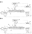
10 テーブル
13 保持面
20 フレーム保持手段
26 昇降手段
30 収縮手段
40 制御手段
51 改質層(分割起点)
C チップ
F リングフレーム
T テープ
W ウエーハ
WS ワークセット
Claims (1)
- リングフレームの開口を塞いで貼着したテープに分割起点が形成されたウエーハを貼着し該リングフレームと該テープとウエーハとを一体化させたワークセットの該テープを拡張させ該分割起点を起点にウエーハを分割する分割装置であって、
該リングフレームを保持するフレーム保持手段と、
該フレーム保持手段が保持したワークセットの該テープを介してウエーハを保持する保持面を有するテーブルと、
該テーブルと該フレーム保持手段とを相対的に該保持面に対して直交する方向で接近および離間させる昇降手段と、
該テーブルと該フレーム保持手段とを離間する方向に移動させ該テープを拡張し該分割起点を起点にウエーハを分割させた後、該テーブルと該フレーム保持手段とを接近する方向に移動させ隣接するチップを近づけて予め設定した狭めた間隔を形成する制御手段と、
該制御手段により該間隔を形成し拡張された該テープを該保持面で吸引保持し該間隔を維持し、該テーブルと該フレーム保持手段とをさらに接近させ、ウエーハの外周とリングフレームの内周との間の弛んだ該テープを収縮させ、隣接するチップの間隔を固定する収縮手段と、を備える分割装置。
Priority Applications (3)
| Application Number | Priority Date | Filing Date | Title |
|---|---|---|---|
| JP2017003235A JP6785162B2 (ja) | 2017-01-12 | 2017-01-12 | 分割装置 |
| TW106142561A TWI734873B (zh) | 2017-01-12 | 2017-12-05 | 分割裝置 |
| KR1020180002330A KR102426263B1 (ko) | 2017-01-12 | 2018-01-08 | 분할 장치 |
Applications Claiming Priority (1)
| Application Number | Priority Date | Filing Date | Title |
|---|---|---|---|
| JP2017003235A JP6785162B2 (ja) | 2017-01-12 | 2017-01-12 | 分割装置 |
Publications (2)
| Publication Number | Publication Date |
|---|---|
| JP2018113349A JP2018113349A (ja) | 2018-07-19 |
| JP6785162B2 true JP6785162B2 (ja) | 2020-11-18 |
Family
ID=62911234
Family Applications (1)
| Application Number | Title | Priority Date | Filing Date |
|---|---|---|---|
| JP2017003235A Active JP6785162B2 (ja) | 2017-01-12 | 2017-01-12 | 分割装置 |
Country Status (3)
| Country | Link |
|---|---|
| JP (1) | JP6785162B2 (ja) |
| KR (1) | KR102426263B1 (ja) |
| TW (1) | TWI734873B (ja) |
Families Citing this family (2)
| Publication number | Priority date | Publication date | Assignee | Title |
|---|---|---|---|---|
| JP7436772B2 (ja) | 2018-12-27 | 2024-02-22 | 日亜化学工業株式会社 | 半導体装置の製造方法 |
| KR102542890B1 (ko) * | 2023-04-03 | 2023-06-13 | 남진우 | 웨이퍼 신장 장치 |
Family Cites Families (13)
| Publication number | Priority date | Publication date | Assignee | Title |
|---|---|---|---|---|
| JP4288392B2 (ja) * | 2003-09-29 | 2009-07-01 | 株式会社東京精密 | エキスパンド方法 |
| JP4744957B2 (ja) | 2005-07-13 | 2011-08-10 | 株式会社ディスコ | ウエーハに装着された接着フィルムの破断装置 |
| JP4955377B2 (ja) * | 2006-12-12 | 2012-06-20 | リンテック株式会社 | チップ間隔の測定装置とその測定方法 |
| TWI463580B (zh) * | 2007-06-19 | 2014-12-01 | Renesas Electronics Corp | Manufacturing method of semiconductor integrated circuit device |
| JP2009094126A (ja) * | 2007-10-04 | 2009-04-30 | Furukawa Electric Co Ltd:The | チップのピックアップ方法 |
| JP5409280B2 (ja) * | 2009-11-09 | 2014-02-05 | 株式会社ディスコ | チップ間隔拡張方法 |
| JP2011216529A (ja) * | 2010-03-31 | 2011-10-27 | Furukawa Electric Co Ltd:The | 半導体装置の製造方法 |
| JP6170681B2 (ja) * | 2013-01-24 | 2017-07-26 | 株式会社ディスコ | 拡張装置および拡張方法 |
| JP6103217B2 (ja) * | 2013-05-30 | 2017-03-29 | 株式会社東京精密 | ワーク分割装置及びワーク分割方法 |
| JP2015204362A (ja) * | 2014-04-14 | 2015-11-16 | 株式会社ディスコ | チップ間隔維持方法 |
| JP2016004832A (ja) | 2014-06-13 | 2016-01-12 | 株式会社ディスコ | テープ拡張装置 |
| CN107408501B (zh) * | 2015-03-24 | 2018-08-24 | 古河电气工业株式会社 | 半导体加工用带 |
| JP5939416B2 (ja) * | 2016-02-12 | 2016-06-22 | 株式会社東京精密 | ワーク分割装置及びワーク分割方法 |
-
2017
- 2017-01-12 JP JP2017003235A patent/JP6785162B2/ja active Active
- 2017-12-05 TW TW106142561A patent/TWI734873B/zh active
-
2018
- 2018-01-08 KR KR1020180002330A patent/KR102426263B1/ko active IP Right Grant
Also Published As
| Publication number | Publication date |
|---|---|
| TWI734873B (zh) | 2021-08-01 |
| JP2018113349A (ja) | 2018-07-19 |
| TW201826373A (zh) | 2018-07-16 |
| KR102426263B1 (ko) | 2022-07-29 |
| KR20180083260A (ko) | 2018-07-20 |
Similar Documents
| Publication | Publication Date | Title |
|---|---|---|
| JP6934327B2 (ja) | ウエーハの分割方法及び分割装置 | |
| TWI687985B (zh) | 分割裝置及晶圓之分割方法 | |
| KR20150118530A (ko) | 칩 간격 유지 방법 | |
| JP5409280B2 (ja) | チップ間隔拡張方法 | |
| JP6266429B2 (ja) | チップ間隔維持装置及びチップ間隔維持方法 | |
| JP2013051368A (ja) | ワーク分割装置及びワーク分割方法 | |
| JP6785162B2 (ja) | 分割装置 | |
| JP7030469B2 (ja) | テープ拡張装置及びテープ拡張方法 | |
| KR102606114B1 (ko) | 웨이퍼의 분할 방법 및 웨이퍼의 분할 장치 | |
| KR102327107B1 (ko) | 분할 장치 및 분할 방법 | |
| KR102225430B1 (ko) | 워크 분할장치 및 워크 분할방법 | |
| US11056361B2 (en) | Laminate processing method | |
| JP6537414B2 (ja) | ウエーハの加工方法 | |
| JP7112205B2 (ja) | 分割装置 | |
| JP5831696B2 (ja) | ダイボンダ | |
| JP2011086866A (ja) | 半導体デバイスの製造方法 | |
| TWI819486B (zh) | 擴展裝置 | |
| JP7130324B2 (ja) | デバイスチップの形成方法 |
Legal Events
| Date | Code | Title | Description |
|---|---|---|---|
| A621 | Written request for application examination |
Free format text: JAPANESE INTERMEDIATE CODE: A621 Effective date: 20191108 |
|
| A977 | Report on retrieval |
Free format text: JAPANESE INTERMEDIATE CODE: A971007 Effective date: 20200918 |
|
| TRDD | Decision of grant or rejection written | ||
| A01 | Written decision to grant a patent or to grant a registration (utility model) |
Free format text: JAPANESE INTERMEDIATE CODE: A01 Effective date: 20200929 |
|
| A61 | First payment of annual fees (during grant procedure) |
Free format text: JAPANESE INTERMEDIATE CODE: A61 Effective date: 20201026 |
|
| R150 | Certificate of patent or registration of utility model |
Ref document number: 6785162 Country of ref document: JP Free format text: JAPANESE INTERMEDIATE CODE: R150 |
|
| R250 | Receipt of annual fees |
Free format text: JAPANESE INTERMEDIATE CODE: R250 |