JP6785162B2 - Split device - Google Patents
Split device Download PDFInfo
- Publication number
- JP6785162B2 JP6785162B2 JP2017003235A JP2017003235A JP6785162B2 JP 6785162 B2 JP6785162 B2 JP 6785162B2 JP 2017003235 A JP2017003235 A JP 2017003235A JP 2017003235 A JP2017003235 A JP 2017003235A JP 6785162 B2 JP6785162 B2 JP 6785162B2
- Authority
- JP
- Japan
- Prior art keywords
- wafer
- tape
- chips
- frame
- holding means
- Prior art date
- Legal status (The legal status is an assumption and is not a legal conclusion. Google has not performed a legal analysis and makes no representation as to the accuracy of the status listed.)
- Active
Links
Images


Classifications
-
- H—ELECTRICITY
- H01—ELECTRIC ELEMENTS
- H01L—SEMICONDUCTOR DEVICES NOT COVERED BY CLASS H10
- H01L21/00—Processes or apparatus adapted for the manufacture or treatment of semiconductor or solid state devices or of parts thereof
- H01L21/67—Apparatus specially adapted for handling semiconductor or electric solid state devices during manufacture or treatment thereof; Apparatus specially adapted for handling wafers during manufacture or treatment of semiconductor or electric solid state devices or components ; Apparatus not specifically provided for elsewhere
- H01L21/67005—Apparatus not specifically provided for elsewhere
- H01L21/67011—Apparatus for manufacture or treatment
- H01L21/67132—Apparatus for placing on an insulating substrate, e.g. tape
-
- H—ELECTRICITY
- H01—ELECTRIC ELEMENTS
- H01L—SEMICONDUCTOR DEVICES NOT COVERED BY CLASS H10
- H01L21/00—Processes or apparatus adapted for the manufacture or treatment of semiconductor or solid state devices or of parts thereof
- H01L21/67—Apparatus specially adapted for handling semiconductor or electric solid state devices during manufacture or treatment thereof; Apparatus specially adapted for handling wafers during manufacture or treatment of semiconductor or electric solid state devices or components ; Apparatus not specifically provided for elsewhere
- H01L21/67005—Apparatus not specifically provided for elsewhere
- H01L21/67011—Apparatus for manufacture or treatment
- H01L21/67092—Apparatus for mechanical treatment
-
- H—ELECTRICITY
- H01—ELECTRIC ELEMENTS
- H01L—SEMICONDUCTOR DEVICES NOT COVERED BY CLASS H10
- H01L21/00—Processes or apparatus adapted for the manufacture or treatment of semiconductor or solid state devices or of parts thereof
- H01L21/67—Apparatus specially adapted for handling semiconductor or electric solid state devices during manufacture or treatment thereof; Apparatus specially adapted for handling wafers during manufacture or treatment of semiconductor or electric solid state devices or components ; Apparatus not specifically provided for elsewhere
- H01L21/683—Apparatus specially adapted for handling semiconductor or electric solid state devices during manufacture or treatment thereof; Apparatus specially adapted for handling wafers during manufacture or treatment of semiconductor or electric solid state devices or components ; Apparatus not specifically provided for elsewhere for supporting or gripping
- H01L21/6835—Apparatus specially adapted for handling semiconductor or electric solid state devices during manufacture or treatment thereof; Apparatus specially adapted for handling wafers during manufacture or treatment of semiconductor or electric solid state devices or components ; Apparatus not specifically provided for elsewhere for supporting or gripping using temporarily an auxiliary support
- H01L21/6836—Wafer tapes, e.g. grinding or dicing support tapes
Description
本発明は、ウエーハを個々のチップに分割する分割装置に関する。 The present invention relates to a dividing device that divides a wafer into individual chips.
従来、この種の分割装置として、リングフレームにテープを介して支持されたウエーハを、テープを拡張することで、ウエーハに形成された分割起点に沿って分割するものが知られている(例えば、特許文献1−3参照)。これら分割装置では、ウエーハが分割テーブルに保持されると共にリングフレームがリング状テーブルに保持されて、リングフレームに対してウエーハが相対的に押し上げられることで、テープが径方向に拡張されてウエーハが個々のチップに分割される。分割後のチップは、次工程においてピッカー等によってテープからピックアップされる。 Conventionally, as this type of dividing device, a wafer supported by a ring frame via a tape is divided by expanding the tape along a division starting point formed in the wafer (for example,). See Patent Document 1-3). In these dividing devices, the wafer is held by the dividing table and the ring frame is held by the ring-shaped table, and the wafer is pushed up relative to the ring frame, so that the tape is expanded in the radial direction and the wafer is expanded. Divided into individual chips. The divided chips are picked up from the tape by a picker or the like in the next step.
ところで、チップサイズが小さなウエーハを分割するためにはテープを大きく拡張する必要がある。テープが大きく拡張されると、チップ同士の間隔が広がり過ぎて、次工程でチップをピックアップできなかったり、ピックアップ時間が長くなったりする。一方で、テープの拡張を抑えてチップ同士の間隔を小さくすることで、チップのピックアップ性を向上させることも考えられるが、チップサイズが小さなウエーハを適切に分割することができない。このように、テープを大きく拡張するとピックアップに不具合が生じ、テープの拡張を抑えるとウエーハを適切に分割できないという問題があった。 By the way, in order to divide a wafer having a small chip size, it is necessary to greatly expand the tape. If the tape is greatly expanded, the distance between the chips becomes too wide, and the chips cannot be picked up in the next process, or the pickup time becomes long. On the other hand, it is conceivable to improve the pick-up property of the chips by suppressing the expansion of the tape and reducing the distance between the chips, but it is not possible to properly divide the wafer having a small chip size. As described above, there is a problem that if the tape is greatly expanded, a problem occurs in the pickup, and if the expansion of the tape is suppressed, the wafer cannot be properly divided.
本発明はかかる点に鑑みてなされたものであり、チップのピックアップ性を悪化させることなく、ウエーハを確実に分割することができる分割装置を提供することを目的の1つとする。 The present invention has been made in view of this point, and one of the objects of the present invention is to provide a dividing device capable of reliably dividing a wafer without deteriorating the pick-up property of the chip.
本発明の一態様の分割装置は、リングフレームの開口を塞いで貼着したテープに分割起点が形成されたウエーハを貼着し該リングフレームと該テープとウエーハとを一体化させたワークセットの該テープを拡張させ該分割起点を起点にウエーハを分割する分割装置であって、該リングフレームを保持するフレーム保持手段と、該フレーム保持手段が保持したワークセットの該テープを介してウエーハを保持する保持面を有するテーブルと、該テーブルと該フレーム保持手段とを相対的に該保持面に対して直交する方向で接近および離間させる昇降手段と、該テーブルと該フレーム保持手段とを離間する方向に移動させ該テープを拡張し該分割起点を起点にウエーハを分割させた後、該テーブルと該フレーム保持手段とを接近する方向に移動させ隣接するチップを近づけて予め設定した狭めた間隔を形成する制御手段と、該制御手段により該間隔を形成し拡張された該テープを該保持面で吸引保持し該間隔を維持し、該テーブルと該フレーム保持手段とをさらに接近させ、ウエーハの外周とリングフレームの内周との間の弛んだ該テープを収縮させ、隣接するチップの間隔を固定する収縮手段と、を備える。 The dividing device of one aspect of the present invention is a work set in which a wafer having a division starting point formed is attached to a tape attached by closing the opening of the ring frame, and the ring frame, the tape, and the wafer are integrated. A dividing device that expands the tape and divides the wafer from the division starting point, and holds the wafer via the frame holding means for holding the ring frame and the tape of the work set held by the frame holding means. A table having a holding surface, an elevating means for bringing the table and the frame holding means closer to each other in a direction relatively orthogonal to the holding surface, and a direction for separating the table and the frame holding means. After the tape is expanded and the wafer is divided starting from the division starting point, the table and the frame holding means are moved in the approaching direction to bring the adjacent chips closer to form a preset narrow interval. The control means and the tape expanded by forming the interval by the control means are sucked and held on the holding surface to maintain the interval, and the table and the frame holding means are further brought closer to the outer periphery of the wafer. A shrinking means for shrinking the loose tape between the inner circumference of the ring frame and fixing the distance between adjacent chips is provided.
この構成によれば、ウエーハの分割時にはテーブルとフレーム保持手段が離間することで、テープが大きく拡張されてウエーハが分割起点を起点にして確実に分割される。ウエーハの分割後にはテーブルとフレーム保持手段が接近することで、テープの拡張が解除されて隣接するチップの間隔が狭められる。そして、隣接するチップの間隔が予め設定した間隔まで狭められた状態で、ウエーハの周囲のテープの弛みが除去されることでチップの間隔が固定される。よって、チップのピックアップ位置にバラツキが生じたり、ピックアップ時間が長くなったりすることがない。このように、チップのピックアップ性を悪化させることなく、ウエーハを確実に分割することができる。 According to this configuration, when the wafer is divided, the table and the frame holding means are separated from each other, so that the tape is greatly expanded and the wafer is surely divided starting from the division starting point. After the wafer is divided, the table and the frame holding means come close to each other, so that the expansion of the tape is released and the distance between adjacent chips is narrowed. Then, in a state where the distance between adjacent chips is narrowed to a preset distance, the gap between the chips is fixed by removing the slack in the tape around the wafer. Therefore, the pickup position of the chip does not vary and the pickup time does not become long. In this way, the wafer can be reliably divided without deteriorating the pick-up property of the chip.
本発明によれば、ウエーハの分割後にテープの拡張が緩められ、隣接するチップの間隔が予め設定した間隔で固定されるようにウエーハの周囲のテープの弛みが除去される。よって、チップのピックアップ性を悪化させることなく、ウエーハを確実に分割することができる。 According to the present invention, the expansion of the tape is loosened after the wafer is divided, and the slack of the tape around the wafer is removed so that the spacing between adjacent chips is fixed at a preset spacing. Therefore, the wafer can be reliably divided without deteriorating the pick-up property of the chip.
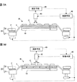
以下、添付図面を参照して、本実施の形態の分割装置について説明する。図1は、本実施の形態の分割装置の斜視図である。図2は、比較例のウエーハの分割動作及びピックアップ動作の説明図である。なお、分割装置は、図1に記載された構成に限定されず、適宜変更することが可能である。 Hereinafter, the dividing device of the present embodiment will be described with reference to the accompanying drawings. FIG. 1 is a perspective view of the dividing device of the present embodiment. FIG. 2 is an explanatory diagram of a wafer division operation and a pickup operation of a comparative example. The dividing device is not limited to the configuration shown in FIG. 1, and can be appropriately changed.
図1に示すように、分割装置1は、リングフレームFにテープTを介して支持されたウエーハWを、テープTの拡張によって個々のチップC(図3A参照)に分割するように構成されている。また、分割装置1は、テープTの拡張の解除時にウエーハWの外周とリングフレームFの内周の間に生じるテープTの弛みを熱収縮(ヒートシュリンク)によって除去するように構成されている。このように、テープTが引き伸ばされて弛んだ箇所だけを熱収縮させて、ウエーハWの分割後のチップC同士が接触して破損しないようにチップCの間隔が維持されている。
As shown in FIG. 1, the
ウエーハWの表面には格子状の分割予定ラインLが設けられており、分割予定ラインLによって区画された各領域に各種デバイス(不図示)が形成されている。なお、ウエーハWは、シリコン、ガリウム砒素等の半導体基板にIC、LSI等のデバイスが形成された半導体ウエーハでもよいし、セラミック、ガラス、サファイア系の無機材料基板にLED等の光デバイスが形成された光デバイスウエーハでもよい。ウエーハWはリングフレームFに貼られたテープTに貼着され、ウエーハWとリングフレームFとテープTを一体化させたワークセットWSが分割装置1に搬入される。
A grid-like division schedule line L is provided on the surface of the wafer W, and various devices (not shown) are formed in each region partitioned by the division schedule line L. The wafer W may be a semiconductor wafer in which devices such as ICs and LSIs are formed on a semiconductor substrate such as silicon or gallium arsenide, or an optical device such as an LED is formed on a ceramic, glass, or sapphire-based inorganic material substrate. It may be an optical device wafer. The wafer W is attached to the tape T attached to the ring frame F, and the work set WS in which the wafer W, the ring frame F, and the tape T are integrated is carried into the
ワークセットWSのリングフレームFは熱収縮性を有するテープTによって開口部が塞がれており、開口部の内側のテープTにウエーハWが貼着されている。ウエーハWの内部には、分割予定ラインLに沿った分割起点として改質層(不図示)が形成されている。なお、改質層は、レーザーの照射によってウエーハWの内部の密度、屈折率、機械的強度やその他の物理的特性が周囲と異なる状態となり、周囲よりも強度が低下する領域のことをいう。改質層は、例えば、溶融処理領域、クラック領域、絶縁破壊領域、屈折率変化領域であり、これらが混在した領域でもよい。 The opening of the ring frame F of the work set WS is closed by the heat-shrinkable tape T, and the wafer W is attached to the tape T inside the opening. Inside the wafer W, a modified layer (not shown) is formed as a division starting point along the planned division line L. The modified layer refers to a region in which the density, refractive index, mechanical strength and other physical properties inside the wafer W are different from those of the surroundings due to laser irradiation, and the strength is lower than that of the surroundings. The modified layer is, for example, a melt processing region, a crack region, a dielectric breakdown region, and a refractive index change region, and may be a region in which these are mixed.
また、以下の説明では、分割起点としてウエーハWの内部に形成された改質層を例示するが、この構成に限定されない。分割起点は、ウエーハWの分割時の起点になればよく、例えば、レーザー加工溝、切削溝、スクライブラインで構成されてもよい。さらに、テープTは、伸縮性を有すると共に熱収縮性を有するものであればよく、特に材質は限定されない。なお、テープ基材は、例えば、PO(Polyolefin)、PVC(Polyvinyl Chloride)で形成されることが好ましい。 Further, in the following description, the modified layer formed inside the wafer W is illustrated as the starting point of division, but the present invention is not limited to this configuration. The division starting point may be the starting point at the time of dividing the wafer W, and may be composed of, for example, a laser machined groove, a cutting groove, and a scribe line. Further, the tape T may be any as long as it has elasticity and heat shrinkage, and the material is not particularly limited. The tape base material is preferably formed of, for example, PO (Polyolefin) or PVC (Polyvinyl Chloride).
分割装置1には、ワークセットWSのテープTを介してウエーハWを吸引保持可能なテーブル10が配置され、テーブル10の周囲にはワークセットWSのリングフレームFを保持するフレーム保持手段20が配置されている。テーブル10は、複数の支柱部11によって支持されており、テーブル10の上面には多孔質のポーラス板12が配置されている。この多孔質のポーラス板12によってテーブル10の上面にウエーハWを吸引保持する保持面13が形成されている。保持面13にはテーブル10内の流路を通じて吸引源16(図4A参照)に接続され、保持面13に生じる負圧によってウエーハWが吸引保持される。
A table 10 capable of sucking and holding the wafer W via the tape T of the work set WS is arranged in the dividing
また、保持面13から吸引源16に連なる流路には開閉バルブ14(図4A参照)が設けられており、開閉バルブ14によってウエーハWに対する保持面13の吸引保持と吸引解除が切り替えられている。テーブル10の外周エッジには、全周に渡って複数のローラ部15が回転可能に設けられている。複数のローラ部15は、保持面13にウエーハWが保持された状態で、ウエーハWの周囲のテープTに下側から転接されている。複数のローラ部15がテープTに転接されることで、テープTの拡張時にテーブル10の外周エッジで生じるテープTの摩擦が抑えられている。
Further, an opening / closing valve 14 (see FIG. 4A) is provided in the flow path connecting the
フレーム保持手段20は、載置テーブル21上のリングフレームFを、カバープレート22で上方から挟み込むようにして、載置テーブル21上にリングフレームFを保持している。載置テーブル21及びカバープレート22の中央には、テーブル10よりも大径の円形開口23、24がそれぞれ形成されている。載置テーブル21上にカバープレート22が被せられると、カバープレート22と載置テーブル21によってリングフレームFが保持されると共に、載置テーブル21及びカバープレート22の円形開口23、24からウエーハWとテープTの一部とが外部に露出される。
The
フレーム保持手段20は、載置テーブル21上のリングフレームFにカバープレート22が被せられた状態で、例えば、不図示のクランプ部によってカバープレート22が載置テーブル21に固定される。フレーム保持手段20は、テーブル10とフレーム保持手段20を、相対的に保持面13に対して直交する方向で離間及び接近させる昇降手段26に支持されている。昇降手段26は、載置テーブル21の四隅を支持する4つの電動シリンダで構成されている。昇降手段26のシリンダロッド27の突出量が制御されることで、テーブル10上のウエーハWとフレーム保持手段20との距離が調節される。
In the
フレーム保持手段20の上方には、テープTに生じた弛みを収縮させる収縮手段30が設けられている。収縮手段30はウエーハWの中心軸上に設けられており、ウエーハWの中心を挟んで対向するように旋回アーム31の両端に一対のヒータ32を配置している。ヒータ32は、例えば、金属材料に吸収され難い3μm〜25μmをピーク波形とする遠赤外線をスポット照射するように構成されている。これにより、装置各部の加熱を抑えてウエーハWの外周とリングフレームFの内周との間のテープTの弛みが部分的に加熱されて熱収縮される。
Above the frame holding means 20, a shrinking means 30 for shrinking the slack generated in the tape T is provided. The contracting means 30 is provided on the central axis of the wafer W, and a pair of
また、収縮手段30の旋回アーム31には、一対のヒータ32を上下動させる上下動作部33と、一対のヒータ32をウエーハWの中心軸回りに回転させる回転モータ34とが設けられている。上下動作部33は、フレーム保持手段20の昇降動作に合わせて、テープTに対する一対のヒータ32の高さを調整する。回転モータ34は、ウエーハWの周囲のテープTの弛みが全周に亘って加熱されるように一対のヒータ32を旋回する。上下動作部33及び回転モータ34によって一対のヒータ32がテープTに対して適切に位置付けられることで、ウエーハWの周囲のテープTが良好に加熱される。
Further, the
また、分割装置1には、装置各部を統括制御する制御手段40が設けられている。制御手段40は、各種処理を実行するプロセッサやメモリ等により構成される。メモリは、用途に応じてROM(Read Only Memory)、RAM(Random Access Memory)等の一つ又は複数の記憶媒体で構成される。制御手段40によってテーブル10とフレーム保持手段20が相対移動されてテープTの拡張動作が制御されると共に、収縮手段30の一対のヒータ32でテープTの弛みが除去されてテープTの収縮動作が制御される。さらに、制御手段40によって後述するチップ間隔の調整処理が制御される。
Further, the
このような分割装置1では、フレーム保持手段20がリングフレームFを保持した状態で下降されることで、カバープレート22及び載置テーブル21の円形開口23、24からテーブル10が突出される。フレーム保持手段20に対してテーブル10が相対的に突き上げられることで、テープTが径方向に拡張されてウエーハWが個々のチップCに分割される。また、フレーム保持手段20が上昇されてテープTの拡張が解除されると、テープTのテンションが緩められる。このとき、ウエーハWの周囲のテープTが弛まないように、ヒータ32によってテープTが加熱されて熱収縮される。
In such a
ところで、図2に示すように、一般的な分割装置61ではウエーハWを分割する度にチップCの間隔にバラツキが生じて、次工程においてピッカー65でチップCをピックアップする際にチップCの位置を認識しなければならない。また、チップサイズの小さなウエーハWを分割するためには、チップC同士が擦れて破損しないようにテープTを大きく拡張する必要があり、ピッカー65でチップCをピックアップする際の移動距離が長くなってピックアップ時間が増大する。さらに、ピッカー65の移動範囲外にチップCが位置付けられると、チップCをピックアップすることができない。
By the way, as shown in FIG. 2, in the general dividing device 61, the interval of the chips C varies every time the wafer W is divided, and the position of the chips C when the
そこで、本実施の形態の分割装置1(図1参照)では、テープTを大きく拡張させてウエーハWを個々のチップCに分割した後に、隣接するチップCの間隔が予め設定した間隔になるようにテープTを緩めている。この場合、テーブル10の上方に設けた外周撮像手段45によって分割後のウエーハWの外周を撮像しながら、撮像画像のウエーハWの外周位置を所定の外周位置に一致させてチップCの間隔を調整している。そして、ウエーハWの周囲のテープTの弛みを熱収縮によって除去することで、隣接するチップCをピックアップ動作に適した間隔で固定するようにしている。 Therefore, in the dividing device 1 (see FIG. 1) of the present embodiment, after the tape T is greatly expanded to divide the wafer W into individual chips C, the intervals between adjacent chips C are set to preset intervals. The tape T is loosened. In this case, the outer peripheral position of the wafer W after division is imaged by the outer peripheral imaging means 45 provided above the table 10, and the outer peripheral position of the wafer W in the captured image is matched with the predetermined outer peripheral position to adjust the interval between the chips C. doing. Then, by removing the slack of the tape T around the wafer W by heat shrinkage, the adjacent chips C are fixed at intervals suitable for the pickup operation.
以下、図3を参照して、制御手段によるチップ間隔の調整処理について説明する。図3は、本実施の形態のチップ間隔の調整処理を示す図である。 Hereinafter, the chip interval adjustment process by the control means will be described with reference to FIG. FIG. 3 is a diagram showing a chip spacing adjustment process of the present embodiment.
図3Aに示すように、フレーム保持手段20に対してテーブル10が相対的に突き上げられると、テープTが拡張されてウエーハWが個々のチップCに分割される。分割後のウエーハWが外径D1まで広げられることで、隣接するチップCの間に間隔S1が形成される。ウエーハWの分割後には、フレーム保持手段20がテーブル10に近づけられてテープTの拡張が解除される。これにより、テープTの弾性回復によって分割後のウエーハWの外径が小さくなり始め、隣接するチップCが徐々に近づけられて、隣接するチップCの間隔が狭められる。 As shown in FIG. 3A, when the table 10 is pushed up relative to the frame holding means 20, the tape T is expanded and the wafer W is divided into individual chips C. By expanding the wafer W after division to the outer diameter D1, an interval S1 is formed between the adjacent chips C. After the wafer W is divided, the frame holding means 20 is brought closer to the table 10 and the expansion of the tape T is released. As a result, the outer diameter of the wafer W after division begins to decrease due to the elastic recovery of the tape T, the adjacent chips C are gradually brought closer to each other, and the distance between the adjacent chips C is narrowed.
このとき、テーブル10の上方には外周撮像手段45が設けられており、外周撮像手段45によって分割後のウエーハWの外周が撮像されている。外周撮像手段45は制御手段40に接続されており、外周撮像手段45から制御手段40にウエーハWの外周の撮像画像が入力されている。制御手段40では、撮像画像に対してエッジ検出処理等の各種画像処理が施されて、撮像画像の輝度差等からウエーハWの外周位置が検出される。上記したように、ウエーハWの分割時にはテープTが拡張されており、外周撮像手段45によってウエーハWの外周位置として外周位置P1が検出される。 At this time, an outer circumference imaging means 45 is provided above the table 10, and the outer circumference of the wafer W after division is imaged by the outer circumference imaging means 45. The outer peripheral imaging means 45 is connected to the control means 40, and an image of the outer circumference of the wafer W is input from the outer peripheral imaging means 45 to the control means 40. In the control means 40, various image processes such as edge detection processing are performed on the captured image, and the outer peripheral position of the wafer W is detected from the difference in brightness of the captured image and the like. As described above, the tape T is expanded when the wafer W is divided, and the outer peripheral position P1 is detected as the outer peripheral position of the wafer W by the outer peripheral imaging means 45.
図3Bに示すように、テーブル10に対するフレーム保持手段20の接近によって、外周撮像手段45で撮像されたウエーハWの外周が外周位置P2まで移動すると、テーブル10の保持面13にテープTが吸引保持されてチップCの間隔が維持される。このとき、ウエーハWが外径D2まで狭められて、隣接するチップCの間に予め設定された間隔S2が形成される。なお、間隔S2は、次工程のピックアップ動作に適した間隔である。このように、隣り合うチップCの間隔に応じて変化するウエーハWの外周位置を外周撮像手段45でモニタして、チップCの間隔を間接的に測定しながらチップCの間隔を調整している。
As shown in FIG. 3B, when the outer circumference of the wafer W imaged by the outer peripheral imaging means 45 moves to the outer peripheral position P2 due to the approach of the frame holding means 20 to the table 10, the tape T is sucked and held on the holding
なお、図3Cに示すように、ウエーハWの外周位置P2は、制御手段40(図3B参照)に接続された算出手段46(図1参照)によって事前に算出されている。より詳細には、ウエーハWのチップサイズによってウエーハWの分割予定ラインの数が決定され、分割予定ラインの数だけチップCを間隔S2まで広げたときのウエーハWの外径D2が算出される。このウエーハWの外径D2に基づいて、チップCの間隔S2に対応したウエーハWの外周位置P2が算出される。なお、算出手段46は、制御手段40と同様に、各種処理を実行するプロセッサやメモリ等により構成される。 As shown in FIG. 3C, the outer peripheral position P2 of the wafer W is calculated in advance by the calculation means 46 (see FIG. 1) connected to the control means 40 (see FIG. 3B). More specifically, the number of planned division lines of the wafer W is determined by the chip size of the wafer W, and the outer diameter D2 of the wafer W when the chip C is expanded to the interval S2 by the number of the scheduled division lines is calculated. Based on the outer diameter D2 of the wafer W, the outer peripheral position P2 of the wafer W corresponding to the interval S2 of the chip C is calculated. The calculation means 46 is composed of a processor, a memory, and the like that execute various processes, like the control means 40.
また、図3Dに示すように、ウエーハWの外周位置P2には、一点鎖線に示すような許容範囲Rが設定されていてもよい。この場合、テーブル10に対するフレーム保持手段20の接近によって、外周撮像手段45で撮像されたウエーハWの外周が許容範囲R内に収まると、隣接するチップCの間隔が予め設定された間隔S2に一致されたと判断される。このようにしてチップCの間隔が調整されると、ウエーハWの周囲のテープTの弛みが熱収縮によって除去されることで、チップCが予め設定した間隔S2を維持した状態で固定される。 Further, as shown in FIG. 3D, the allowable range R as shown by the alternate long and short dash line may be set at the outer peripheral position P2 of the wafer W. In this case, when the outer circumference of the wafer W imaged by the outer peripheral imaging means 45 falls within the permissible range R due to the approach of the frame holding means 20 to the table 10, the interval between the adjacent chips C coincides with the preset interval S2. It is judged that it was done. When the interval between the chips C is adjusted in this way, the slack of the tape T around the wafer W is removed by heat shrinkage, so that the chip C is fixed in a state where the preset interval S2 is maintained.
続いて、図4を参照して、本実施の形態の分割装置による分割動作について説明する。図4は、本実施の形態の分割装置による分割動作の説明図である。図4Aは分割工程の一例、図4Bはチップ間隔調整工程の一例、図4Cはテープ吸引保持工程の一例、図4Dはテープ収縮工程の一例をそれぞれ示している。 Subsequently, the division operation by the division device of the present embodiment will be described with reference to FIG. FIG. 4 is an explanatory diagram of a division operation by the division device of the present embodiment. 4A shows an example of a dividing step, FIG. 4B shows an example of a chip spacing adjusting step, FIG. 4C shows an example of a tape suction holding step, and FIG. 4D shows an example of a tape shrinking step.
図4Aに示すように、先ず分割工程が実施される。分割工程では、テーブル10上にテープTを介してウエーハWが載置され、ウエーハWの周囲のリングフレームFがフレーム保持手段20に保持される。このとき、開閉バルブ14が閉じられており、吸引源16からのテーブル10への吸引力が遮断されている。そして、制御手段40の制御によってフレーム保持手段20が下降されて、テーブル10とフレーム保持手段20が離間される。これにより、テープTが放射方向に拡張されて、テープTを介して強度が低下した改質層を起点にしてウエーハWが個々のチップCに分割される。
As shown in FIG. 4A, the division step is first carried out. In the dividing step, the wafer W is placed on the table 10 via the tape T, and the ring frame F around the wafer W is held by the frame holding means 20. At this time, the on-off
図4Bに示すように、分割工程の後にチップ間隔調整工程が実施される。チップ間隔調整工程では、制御手段40の制御によってフレーム保持手段20が上昇されて、テーブル10とフレーム保持手段20が接近される。これにより、テープTの拡張が解除されて、テープTの弾性回復によって隣接するチップCが徐々に近づけられる。このとき、テーブル10の上方に外周撮像手段45が位置付けられており、分割されたウエーハWの外周が外周撮像手段45によって撮像されている。この撮像画像からウエーハWの外周位置が検出され、算出手段46(図1参照)によって予め算出されたウエーハWの外周位置と比較される。 As shown in FIG. 4B, a chip spacing adjusting step is performed after the dividing step. In the chip spacing adjusting step, the frame holding means 20 is raised by the control of the control means 40, and the table 10 and the frame holding means 20 are brought close to each other. As a result, the expansion of the tape T is released, and the elastic recovery of the tape T gradually brings the adjacent chips C closer to each other. At this time, the outer peripheral imaging means 45 is positioned above the table 10, and the outer circumference of the divided wafer W is imaged by the outer peripheral imaging means 45. The outer peripheral position of the wafer W is detected from this captured image and compared with the outer peripheral position of the wafer W calculated in advance by the calculation means 46 (see FIG. 1).
撮像画像から検出されたウエーハWの外周位置が、予め算出されたウエーハWの外周位置に一致するまで、制御手段40によってテーブル10とフレーム保持手段20が接近される。隣接するチップCが徐々に近づけられて、チップCの間隔が予め設定した間隔に調整される。チップCの間隔調整時には開閉バルブ14が閉じられているため、テーブル10によってテープTの変形が阻害されることがない。また、テーブル10とフレーム保持手段20の接近によって、ウエーハWの外周とリングフレームFの内周の間のテープTのテンションが緩んでウエーハWの周囲のテープTに弛みが発生する。
The control means 40 brings the table 10 and the frame holding means 20 closer to each other until the outer peripheral position of the wafer W detected from the captured image matches the pre-calculated outer peripheral position of the wafer W. Adjacent chips C are gradually brought closer to each other, and the distance between the chips C is adjusted to a preset distance. Since the on-off
図4Cに示すように、チップ間隔調整工程の後にテープ吸引保持工程が実施される。テープ吸引保持工程では、制御手段40によってチップCの間に予め設定した間隔が形成されると、開閉バルブ14が開かれてテーブル10に吸引力が発生する。テーブル10によってテープTを介してチップCが吸引保持されるため、テープTが弾性回復によって収縮することなく隣接するチップCが予め設定した間隔を空けて維持される。また、ウエーハWの上方に収縮手段30が位置付けられ、回転モータ34によって一対のヒータ32が旋回されてテープTの弛みの熱収縮が開始される。
As shown in FIG. 4C, a tape suction holding step is performed after the chip spacing adjusting step. In the tape suction holding step, when a preset interval is formed between the chips C by the control means 40, the opening / closing
図4Dに示すように、テープ吸引保持工程の後にテープ収縮工程が実施される。テープ収縮工程では、制御手段40によってテーブル10とフレーム保持手段20がさらに接近されることで、ウエーハWの外周とリングフレームFの内周の間のテープTの弛みが発生する。このとき、フレーム保持手段20の移動に合わせて、上下動作部33によってヒータ32の高さが調整されながら一対のヒータ32によってウエーハWの周囲のテープTの弛みが熱収縮される。ウエーハWの周囲のテープTだけが熱収縮されるため、テーブル10の吸引保持が解除されても隣接するチップCの間隔が維持された状態で固定される。
As shown in FIG. 4D, a tape shrinking step is performed after the tape suction holding step. In the tape shrinking step, the control means 40 brings the table 10 and the frame holding means 20 closer to each other, so that the tape T is loosened between the outer circumference of the wafer W and the inner circumference of the ring frame F. At this time, the slack of the tape T around the wafer W is thermally contracted by the pair of
そして、テープ収縮工程後は開閉バルブ14が閉じられ、テーブル10によるテープTの吸引が解除されてワークセットWSの搬送を可能にしている。このように、ウエーハWの分割後に隣接するチップCの間隔が予め設定した間隔で固定されるため、チップCの間隔が広すぎることがなく、次工程のピックアップ動作時にピッカーの移動距離を短くしてピックアップ時間を短縮することができる。また、ウエーハWの分割後にチップCのバラツキが生じないため、ピッカーを規定の動作プログラムに従って動かすことで、全てのチップCを適切にピックアップさせることができる。
Then, after the tape shrinking step, the opening / closing
以上のように、本実施の形態の分割装置1では、ウエーハWの分割時にはテーブル10とフレーム保持手段20が離間することで、テープTが大きく拡張されてウエーハWが改質層を起点にして確実に分割される。ウエーハWの分割後にはテーブル10とフレーム保持手段20が接近することで、テープTの拡張が解除されて隣接するチップCの間隔が狭められる。そして、隣接するチップCの間隔が予め設定した間隔まで狭められた状態で、ウエーハWの周囲のテープTの弛みが除去されることでチップCの間隔が固定される。よって、チップCのピックアップ位置にバラツキが生じたり、ピックアップ時間が長くなったりすることがない。このように、チップCのピックアップ性を悪化させることなく、ウエーハWを確実に分割することができる。
As described above, in the
なお、本実施の形態では、分割されたウエーハの外周位置を撮像して、ウエーハの外周位置を基準に隣接するチップの間隔を調整する構成にしたが、この構成に限定されない。隣接するチップの間隔が予め設定された間隔に調整される構成であれば、どのようにチップの間隔が調整されてもよい。例えば、分割されたウエーハを撮像して、撮像画像から隣接するチップの間隔を測定しながら、チップの間隔を調整する構成にしてもよい。 In the present embodiment, the outer peripheral position of the divided wafer is imaged and the distance between adjacent chips is adjusted with reference to the outer peripheral position of the wafer, but the configuration is not limited to this. The chip spacing may be adjusted in any way as long as the spacing between adjacent chips is adjusted to a preset spacing. For example, the divided wafer may be imaged and the distance between adjacent chips may be adjusted from the captured image while adjusting the distance between the chips.
具体的には、図5Aに示すように、テープTの拡張によってウエーハWが分割されると、隣接するチップCの間に間隔S1が形成される。ウエーハの分割後には、テープTの拡張が解除されて、テープTの弾性回復によって隣接するチップCが徐々に近づけられる。このとき、テーブル10の上方には撮像手段48が設けられており、撮像手段48によって分割後のウエーハWが撮像されている。撮像手段48には測定手段49が接続されており、撮像手段48から入力された撮像画像に対して各種画像処理が施されて、測定手段49によって隣接するチップCの間隔が測定される。 Specifically, as shown in FIG. 5A, when the wafer W is divided by the expansion of the tape T, an interval S1 is formed between the adjacent chips C. After the wafer is divided, the expansion of the tape T is released, and the elastic recovery of the tape T gradually brings the adjacent chips C closer to each other. At this time, an imaging means 48 is provided above the table 10, and the divided wafer W is imaged by the imaging means 48. A measuring means 49 is connected to the imaging means 48, various image processing is performed on the captured image input from the imaging means 48, and the interval between adjacent chips C is measured by the measuring means 49.
そして、図5Bに示すように、テーブル10に対するフレーム保持手段20の接近によって、測定手段49が測定したチップCの間隔が予め設定された間隔S2に一致すると、テーブル10によってテープTが吸引保持されてチップCの間隔が維持される。このように、隣り合うチップCの間隔を撮像手段48でモニタして、チップCの間隔を直接的に測定しながらチップCの間隔を調整している。なお、測定手段49は、制御手段40と同様に、各種処理を実行するプロセッサやメモリ等により構成される。 Then, as shown in FIG. 5B, when the interval of the chips C measured by the measuring means 49 coincides with the preset interval S2 due to the approach of the frame holding means 20 to the table 10, the tape T is sucked and held by the table 10. The spacing between chips C is maintained. In this way, the distance between adjacent chips C is monitored by the imaging means 48, and the distance between the chips C is adjusted while directly measuring the distance between the chips C. The measuring means 49, like the control means 40, is composed of a processor, a memory, and the like that execute various processes.
また、本実施の形態では、昇降手段がテーブルに対してフレーム保持手段を昇降させる構成にしたが、この構成に限定されない。昇降手段は、テーブルとフレーム保持手段とを相対的に接近及び離間させる構成であればよく、例えば、フレーム保持手段に対してテーブルを昇降させる構成にしてもよい。また、昇降手段は電動シリンダに限定されず、他のアクチュエータで構成されていてもよい。 Further, in the present embodiment, the elevating means raises and lowers the frame holding means with respect to the table, but the present invention is not limited to this configuration. The elevating means may have a configuration in which the table and the frame holding means are relatively close to each other and separated from each other. For example, the elevating means may be configured to raise and lower the table with respect to the frame holding means. Further, the elevating means is not limited to the electric cylinder, and may be composed of other actuators.
また、本実施の形態では、外周撮像手段はウエーハの外周を撮像可能な構成であればよく、例えば、CCD(Charged Coupled Device)、CMOS(Complementary Metal Oxide Semiconductor)等の撮像素子が用いられてもよい。また、変形例の撮像手段はウエーハを撮像可能な構成であればよく、例えば、CCD、CMOS等の撮像素子が用いられてもよい。 Further, in the present embodiment, the outer peripheral imaging means may have a configuration capable of imaging the outer circumference of the wafer, and even if an imaging element such as a CCD (Charged Coupled Device) or a CMOS (Complementary Metal Oxide Semiconductor) is used, for example. Good. Further, the imaging means of the modified example may have a configuration capable of imaging a wafer, and for example, an imaging element such as CCD or CMOS may be used.
また、本発明の実施の形態を説明したが、本発明の他の実施の形態として、上記実施の形態及び変形例を全体的又は部分的に組み合わせたものでもよい。 Moreover, although the embodiment of the present invention has been described, as another embodiment of the present invention, the above-described embodiment and modifications may be combined in whole or in part.
また、本発明の実施の形態は上記の実施の形態及び変形例に限定されるものではなく、本発明の技術的思想の趣旨を逸脱しない範囲において様々に変更、置換、変形されてもよい。さらには、技術の進歩又は派生する別技術によって、本発明の技術的思想を別の仕方で実現することができれば、その方法を用いて実施されてもよい。したがって、特許請求の範囲は、本発明の技術的思想の範囲内に含まれ得る全ての実施形態をカバーしている。 Further, the embodiment of the present invention is not limited to the above-described embodiment and modification, and may be variously modified, replaced, or modified without departing from the spirit of the technical idea of the present invention. Furthermore, if the technical idea of the present invention can be realized in another way by the advancement of technology or another technology derived from it, it may be carried out by using that method. Therefore, the scope of claims covers all embodiments that may be included within the scope of the technical idea of the present invention.
また、本実施の形態では、本発明を分割装置に適用した構成について説明したが、テープを適切に拡張する他のエキスパンド装置に適用することも可能である。 Further, in the present embodiment, the configuration in which the present invention is applied to the dividing device has been described, but it is also possible to apply the present invention to other expanding devices that appropriately expand the tape.
以上説明したように、本発明は、チップのピックアップ性を悪化させることなく、ウエーハを確実に分割することができるという効果を有し、特に、半導体ウエーハを分割する分割装置に有用である。 As described above, the present invention has an effect that the wafer can be reliably divided without deteriorating the pick-up property of the chip, and is particularly useful for a dividing device for dividing a semiconductor wafer.
1 分割装置
10 テーブル
13 保持面
20 フレーム保持手段
26 昇降手段
30 収縮手段
40 制御手段
51 改質層(分割起点)
C チップ
F リングフレーム
T テープ
W ウエーハ
WS ワークセット
1
C Chip F Ring Frame T Tape W Wafer WS Workset
Claims (1)
該リングフレームを保持するフレーム保持手段と、
該フレーム保持手段が保持したワークセットの該テープを介してウエーハを保持する保持面を有するテーブルと、
該テーブルと該フレーム保持手段とを相対的に該保持面に対して直交する方向で接近および離間させる昇降手段と、
該テーブルと該フレーム保持手段とを離間する方向に移動させ該テープを拡張し該分割起点を起点にウエーハを分割させた後、該テーブルと該フレーム保持手段とを接近する方向に移動させ隣接するチップを近づけて予め設定した狭めた間隔を形成する制御手段と、
該制御手段により該間隔を形成し拡張された該テープを該保持面で吸引保持し該間隔を維持し、該テーブルと該フレーム保持手段とをさらに接近させ、ウエーハの外周とリングフレームの内周との間の弛んだ該テープを収縮させ、隣接するチップの間隔を固定する収縮手段と、を備える分割装置。 A wafer having a division starting point formed is attached to a tape attached by closing the opening of the ring frame, and the tape of the work set in which the ring frame, the tape, and the wafer are integrated is expanded to start from the division starting point. It is a dividing device that divides the wafer into
A frame holding means for holding the ring frame and
A table having a holding surface for holding the wafer through the tape of the work set held by the frame holding means,
An elevating means for bringing the table and the frame holding means closer to each other and separated from the holding surface in a direction orthogonal to the holding surface.
The table and the frame holding means are moved in a direction to be separated from each other, the tape is expanded, the wafer is divided from the starting point of the division, and then the table and the frame holding means are moved in a direction of approaching and adjacent to each other. A control means that brings the chips closer together to form a preset narrow interval,
The tape formed and expanded by the control means is sucked and held on the holding surface to maintain the gap, the table and the frame holding means are further brought closer to each other, and the outer circumference of the wafer and the inner circumference of the ring frame are further brought closer. A splitting device comprising a shrinking means for shrinking the loose tape between the two and fixing the spacing between adjacent chips.
Priority Applications (3)
| Application Number | Priority Date | Filing Date | Title |
|---|---|---|---|
| JP2017003235A JP6785162B2 (en) | 2017-01-12 | 2017-01-12 | Split device |
| TW106142561A TWI734873B (en) | 2017-01-12 | 2017-12-05 | Split device |
| KR1020180002330A KR102426263B1 (en) | 2017-01-12 | 2018-01-08 | Dividing apparatus |
Applications Claiming Priority (1)
| Application Number | Priority Date | Filing Date | Title |
|---|---|---|---|
| JP2017003235A JP6785162B2 (en) | 2017-01-12 | 2017-01-12 | Split device |
Publications (2)
| Publication Number | Publication Date |
|---|---|
| JP2018113349A JP2018113349A (en) | 2018-07-19 |
| JP6785162B2 true JP6785162B2 (en) | 2020-11-18 |
Family
ID=62911234
Family Applications (1)
| Application Number | Title | Priority Date | Filing Date |
|---|---|---|---|
| JP2017003235A Active JP6785162B2 (en) | 2017-01-12 | 2017-01-12 | Split device |
Country Status (3)
| Country | Link |
|---|---|
| JP (1) | JP6785162B2 (en) |
| KR (1) | KR102426263B1 (en) |
| TW (1) | TWI734873B (en) |
Families Citing this family (2)
| Publication number | Priority date | Publication date | Assignee | Title |
|---|---|---|---|---|
| JP7436772B2 (en) | 2018-12-27 | 2024-02-22 | 日亜化学工業株式会社 | Manufacturing method of semiconductor device |
| KR102542890B1 (en) * | 2023-04-03 | 2023-06-13 | 남진우 | Wafer elongation device |
Family Cites Families (13)
| Publication number | Priority date | Publication date | Assignee | Title |
|---|---|---|---|---|
| JP4288392B2 (en) * | 2003-09-29 | 2009-07-01 | 株式会社東京精密 | Expanding method |
| JP4744957B2 (en) | 2005-07-13 | 2011-08-10 | 株式会社ディスコ | Breaker for adhesive film mounted on wafer |
| JP4955377B2 (en) * | 2006-12-12 | 2012-06-20 | リンテック株式会社 | Chip spacing measuring device and measuring method |
| TWI463580B (en) * | 2007-06-19 | 2014-12-01 | Renesas Electronics Corp | Manufacturing method of semiconductor integrated circuit device |
| JP2009094126A (en) * | 2007-10-04 | 2009-04-30 | Furukawa Electric Co Ltd:The | Pickup method for chip |
| JP5409280B2 (en) | 2009-11-09 | 2014-02-05 | 株式会社ディスコ | Tip interval expansion method |
| JP2011216529A (en) * | 2010-03-31 | 2011-10-27 | Furukawa Electric Co Ltd:The | Method for manufacturing semiconductor device |
| JP6170681B2 (en) | 2013-01-24 | 2017-07-26 | 株式会社ディスコ | Expansion device and expansion method |
| JP6103217B2 (en) * | 2013-05-30 | 2017-03-29 | 株式会社東京精密 | Work dividing apparatus and work dividing method |
| JP2015204362A (en) * | 2014-04-14 | 2015-11-16 | 株式会社ディスコ | chip interval maintenance method |
| JP2016004832A (en) | 2014-06-13 | 2016-01-12 | 株式会社ディスコ | Tape extension device |
| KR101894690B1 (en) * | 2015-03-24 | 2018-09-04 | 후루카와 덴키 고교 가부시키가이샤 | Tape for semiconductor processing |
| JP5939416B2 (en) | 2016-02-12 | 2016-06-22 | 株式会社東京精密 | Work dividing apparatus and work dividing method |
-
2017
- 2017-01-12 JP JP2017003235A patent/JP6785162B2/en active Active
- 2017-12-05 TW TW106142561A patent/TWI734873B/en active
-
2018
- 2018-01-08 KR KR1020180002330A patent/KR102426263B1/en active IP Right Grant
Also Published As
| Publication number | Publication date |
|---|---|
| JP2018113349A (en) | 2018-07-19 |
| KR102426263B1 (en) | 2022-07-29 |
| KR20180083260A (en) | 2018-07-20 |
| TWI734873B (en) | 2021-08-01 |
| TW201826373A (en) | 2018-07-16 |
Similar Documents
| Publication | Publication Date | Title |
|---|---|---|
| JP6934327B2 (en) | Wafer division method and division device | |
| JP6570942B2 (en) | Dividing device and wafer dividing method | |
| KR20150118530A (en) | Method for maintaining spaces between chips | |
| JP5409280B2 (en) | Tip interval expansion method | |
| JP6266429B2 (en) | Chip interval maintaining device and chip interval maintaining method | |
| JP6785162B2 (en) | Split device | |
| KR102606114B1 (en) | Wafer dividing method and wafer dividing apparatus | |
| KR102327107B1 (en) | Dividing apparatus and dividing method | |
| US11056361B2 (en) | Laminate processing method | |
| JP6537414B2 (en) | Wafer processing method | |
| CN110164810B (en) | Dividing apparatus and dividing method | |
| JP7112205B2 (en) | splitter | |
| JP5831696B2 (en) | Die bonder | |
| JP2011086866A (en) | Method of manufacturing semiconductor device | |
| TWI819486B (en) | expansion device | |
| JP7130324B2 (en) | Device chip forming method | |
| JP2021019163A (en) | Manufacturing method of chip |
Legal Events
| Date | Code | Title | Description |
|---|---|---|---|
| A621 | Written request for application examination |
Free format text: JAPANESE INTERMEDIATE CODE: A621 Effective date: 20191108 |
|
| A977 | Report on retrieval |
Free format text: JAPANESE INTERMEDIATE CODE: A971007 Effective date: 20200918 |
|
| TRDD | Decision of grant or rejection written | ||
| A01 | Written decision to grant a patent or to grant a registration (utility model) |
Free format text: JAPANESE INTERMEDIATE CODE: A01 Effective date: 20200929 |
|
| A61 | First payment of annual fees (during grant procedure) |
Free format text: JAPANESE INTERMEDIATE CODE: A61 Effective date: 20201026 |
|
| R150 | Certificate of patent or registration of utility model |
Ref document number: 6785162 Country of ref document: JP Free format text: JAPANESE INTERMEDIATE CODE: R150 |
|
| R250 | Receipt of annual fees |
Free format text: JAPANESE INTERMEDIATE CODE: R250 |