JP7436772B2 - Manufacturing method of semiconductor device - Google Patents
Manufacturing method of semiconductor device Download PDFInfo
- Publication number
- JP7436772B2 JP7436772B2 JP2018246087A JP2018246087A JP7436772B2 JP 7436772 B2 JP7436772 B2 JP 7436772B2 JP 2018246087 A JP2018246087 A JP 2018246087A JP 2018246087 A JP2018246087 A JP 2018246087A JP 7436772 B2 JP7436772 B2 JP 7436772B2
- Authority
- JP
- Japan
- Prior art keywords
- semiconductor
- stretchable film
- semiconductor element
- semiconductor elements
- manufacturing
- Prior art date
- Legal status (The legal status is an assumption and is not a legal conclusion. Google has not performed a legal analysis and makes no representation as to the accuracy of the status listed.)
- Active
Links
- 239000004065 semiconductor Substances 0.000 title claims description 692
- 238000004519 manufacturing process Methods 0.000 title claims description 132
- 238000000034 method Methods 0.000 claims description 234
- 239000000758 substrate Substances 0.000 claims description 100
- 238000005498 polishing Methods 0.000 claims description 16
- 229920006302 stretch film Polymers 0.000 claims description 8
- 238000006243 chemical reaction Methods 0.000 description 24
- 229920005989 resin Polymers 0.000 description 19
- 239000011347 resin Substances 0.000 description 19
- 239000000463 material Substances 0.000 description 16
- VYPSYNLAJGMNEJ-UHFFFAOYSA-N Silicium dioxide Chemical compound O=[Si]=O VYPSYNLAJGMNEJ-UHFFFAOYSA-N 0.000 description 13
- 239000011230 binding agent Substances 0.000 description 7
- 229910052693 Europium Inorganic materials 0.000 description 4
- XLOMVQKBTHCTTD-UHFFFAOYSA-N Zinc monoxide Chemical compound [Zn]=O XLOMVQKBTHCTTD-UHFFFAOYSA-N 0.000 description 4
- OGPBJKLSAFTDLK-UHFFFAOYSA-N europium atom Chemical compound [Eu] OGPBJKLSAFTDLK-UHFFFAOYSA-N 0.000 description 4
- 239000000945 filler Substances 0.000 description 4
- 150000004767 nitrides Chemical class 0.000 description 4
- 239000000126 substance Substances 0.000 description 4
- 229910052684 Cerium Inorganic materials 0.000 description 3
- OAICVXFJPJFONN-UHFFFAOYSA-N Phosphorus Chemical compound [P] OAICVXFJPJFONN-UHFFFAOYSA-N 0.000 description 3
- GWXLDORMOJMVQZ-UHFFFAOYSA-N cerium Chemical compound [Ce] GWXLDORMOJMVQZ-UHFFFAOYSA-N 0.000 description 3
- 239000011248 coating agent Substances 0.000 description 3
- 238000000576 coating method Methods 0.000 description 3
- 239000011159 matrix material Substances 0.000 description 3
- 229920002050 silicone resin Polymers 0.000 description 3
- 229910052582 BN Inorganic materials 0.000 description 2
- PZNSFCLAULLKQX-UHFFFAOYSA-N Boron nitride Chemical compound N#B PZNSFCLAULLKQX-UHFFFAOYSA-N 0.000 description 2
- RYGMFSIKBFXOCR-UHFFFAOYSA-N Copper Chemical compound [Cu] RYGMFSIKBFXOCR-UHFFFAOYSA-N 0.000 description 2
- 238000005516 engineering process Methods 0.000 description 2
- 239000002223 garnet Substances 0.000 description 2
- -1 lutetium aluminum Chemical compound 0.000 description 2
- TWNQGVIAIRXVLR-UHFFFAOYSA-N oxo(oxoalumanyloxy)alumane Chemical compound O=[Al]O[Al]=O TWNQGVIAIRXVLR-UHFFFAOYSA-N 0.000 description 2
- 239000000843 powder Substances 0.000 description 2
- 229910052814 silicon oxide Inorganic materials 0.000 description 2
- 239000011787 zinc oxide Substances 0.000 description 2
- PFNQVRZLDWYSCW-UHFFFAOYSA-N (fluoren-9-ylideneamino) n-naphthalen-1-ylcarbamate Chemical compound C12=CC=CC=C2C2=CC=CC=C2C1=NOC(=O)NC1=CC=CC2=CC=CC=C12 PFNQVRZLDWYSCW-UHFFFAOYSA-N 0.000 description 1
- 229920000178 Acrylic resin Polymers 0.000 description 1
- 239000004925 Acrylic resin Substances 0.000 description 1
- 229920002799 BoPET Polymers 0.000 description 1
- VYZAMTAEIAYCRO-UHFFFAOYSA-N Chromium Chemical compound [Cr] VYZAMTAEIAYCRO-UHFFFAOYSA-N 0.000 description 1
- BPQQTUXANYXVAA-UHFFFAOYSA-N Orthosilicate Chemical compound [O-][Si]([O-])([O-])[O-] BPQQTUXANYXVAA-UHFFFAOYSA-N 0.000 description 1
- 241001290864 Schoenoplectus Species 0.000 description 1
- 229920002600 TPX™ Polymers 0.000 description 1
- GWEVSGVZZGPLCZ-UHFFFAOYSA-N Titan oxide Chemical compound O=[Ti]=O GWEVSGVZZGPLCZ-UHFFFAOYSA-N 0.000 description 1
- 239000005083 Zinc sulfide Substances 0.000 description 1
- 230000002411 adverse Effects 0.000 description 1
- FNCIDSNKNZQJTJ-UHFFFAOYSA-N alumane;terbium Chemical compound [AlH3].[Tb] FNCIDSNKNZQJTJ-UHFFFAOYSA-N 0.000 description 1
- JNDMLEXHDPKVFC-UHFFFAOYSA-N aluminum;oxygen(2-);yttrium(3+) Chemical compound [O-2].[O-2].[O-2].[Al+3].[Y+3] JNDMLEXHDPKVFC-UHFFFAOYSA-N 0.000 description 1
- 239000000404 calcium aluminium silicate Substances 0.000 description 1
- 235000012215 calcium aluminium silicate Nutrition 0.000 description 1
- WNCYAPRTYDMSFP-UHFFFAOYSA-N calcium aluminosilicate Chemical compound [Al+3].[Al+3].[Ca+2].[O-][Si]([O-])=O.[O-][Si]([O-])=O.[O-][Si]([O-])=O.[O-][Si]([O-])=O WNCYAPRTYDMSFP-UHFFFAOYSA-N 0.000 description 1
- 229940078583 calcium aluminosilicate Drugs 0.000 description 1
- 229910052804 chromium Inorganic materials 0.000 description 1
- 239000011651 chromium Substances 0.000 description 1
- 238000000748 compression moulding Methods 0.000 description 1
- 229910052802 copper Inorganic materials 0.000 description 1
- 239000010949 copper Substances 0.000 description 1
- 239000011889 copper foil Substances 0.000 description 1
- PMHQVHHXPFUNSP-UHFFFAOYSA-M copper(1+);methylsulfanylmethane;bromide Chemical compound Br[Cu].CSC PMHQVHHXPFUNSP-UHFFFAOYSA-M 0.000 description 1
- 238000010586 diagram Methods 0.000 description 1
- NJLLQSBAHIKGKF-UHFFFAOYSA-N dipotassium dioxido(oxo)titanium Chemical compound [K+].[K+].[O-][Ti]([O-])=O NJLLQSBAHIKGKF-UHFFFAOYSA-N 0.000 description 1
- 238000007599 discharging Methods 0.000 description 1
- 229920001971 elastomer Polymers 0.000 description 1
- 239000003822 epoxy resin Substances 0.000 description 1
- 238000005530 etching Methods 0.000 description 1
- 239000011521 glass Substances 0.000 description 1
- 239000003365 glass fiber Substances 0.000 description 1
- 230000002452 interceptive effect Effects 0.000 description 1
- WPBNNNQJVZRUHP-UHFFFAOYSA-L manganese(2+);methyl n-[[2-(methoxycarbonylcarbamothioylamino)phenyl]carbamothioyl]carbamate;n-[2-(sulfidocarbothioylamino)ethyl]carbamodithioate Chemical compound [Mn+2].[S-]C(=S)NCCNC([S-])=S.COC(=O)NC(=S)NC1=CC=CC=C1NC(=S)NC(=O)OC WPBNNNQJVZRUHP-UHFFFAOYSA-L 0.000 description 1
- 239000007769 metal material Substances 0.000 description 1
- 238000012986 modification Methods 0.000 description 1
- 230000004048 modification Effects 0.000 description 1
- QJGQUHMNIGDVPM-UHFFFAOYSA-N nitrogen group Chemical group [N] QJGQUHMNIGDVPM-UHFFFAOYSA-N 0.000 description 1
- 239000005011 phenolic resin Substances 0.000 description 1
- 239000004033 plastic Substances 0.000 description 1
- 229920003023 plastic Polymers 0.000 description 1
- 239000002985 plastic film Substances 0.000 description 1
- 229920006255 plastic film Polymers 0.000 description 1
- 229920000636 poly(norbornene) polymer Polymers 0.000 description 1
- 229920005668 polycarbonate resin Polymers 0.000 description 1
- 239000004431 polycarbonate resin Substances 0.000 description 1
- 229920000647 polyepoxide Polymers 0.000 description 1
- 229920001721 polyimide Polymers 0.000 description 1
- 229920001296 polysiloxane Polymers 0.000 description 1
- HBMJWWWQQXIZIP-UHFFFAOYSA-N silicon carbide Chemical compound [Si+]#[C-] HBMJWWWQQXIZIP-UHFFFAOYSA-N 0.000 description 1
- 229910010271 silicon carbide Inorganic materials 0.000 description 1
- 239000000377 silicon dioxide Substances 0.000 description 1
- 229920002803 thermoplastic polyurethane Polymers 0.000 description 1
- OGIDPMRJRNCKJF-UHFFFAOYSA-N titanium oxide Inorganic materials [Ti]=O OGIDPMRJRNCKJF-UHFFFAOYSA-N 0.000 description 1
- 238000001721 transfer moulding Methods 0.000 description 1
- 229910019901 yttrium aluminum garnet Inorganic materials 0.000 description 1
- 229910052984 zinc sulfide Inorganic materials 0.000 description 1
- DRDVZXDWVBGGMH-UHFFFAOYSA-N zinc;sulfide Chemical compound [S-2].[Zn+2] DRDVZXDWVBGGMH-UHFFFAOYSA-N 0.000 description 1
Images


Classifications
-
- H—ELECTRICITY
- H01—ELECTRIC ELEMENTS
- H01L—SEMICONDUCTOR DEVICES NOT COVERED BY CLASS H10
- H01L33/00—Semiconductor devices with at least one potential-jump barrier or surface barrier specially adapted for light emission; Processes or apparatus specially adapted for the manufacture or treatment thereof or of parts thereof; Details thereof
- H01L33/005—Processes
- H01L33/0095—Post-treatment of devices, e.g. annealing, recrystallisation or short-circuit elimination
-
- H—ELECTRICITY
- H01—ELECTRIC ELEMENTS
- H01L—SEMICONDUCTOR DEVICES NOT COVERED BY CLASS H10
- H01L25/00—Assemblies consisting of a plurality of individual semiconductor or other solid state devices ; Multistep manufacturing processes thereof
- H01L25/03—Assemblies consisting of a plurality of individual semiconductor or other solid state devices ; Multistep manufacturing processes thereof all the devices being of a type provided for in the same subgroup of groups H01L27/00 - H01L33/00, or in a single subclass of H10K, H10N, e.g. assemblies of rectifier diodes
- H01L25/04—Assemblies consisting of a plurality of individual semiconductor or other solid state devices ; Multistep manufacturing processes thereof all the devices being of a type provided for in the same subgroup of groups H01L27/00 - H01L33/00, or in a single subclass of H10K, H10N, e.g. assemblies of rectifier diodes the devices not having separate containers
- H01L25/075—Assemblies consisting of a plurality of individual semiconductor or other solid state devices ; Multistep manufacturing processes thereof all the devices being of a type provided for in the same subgroup of groups H01L27/00 - H01L33/00, or in a single subclass of H10K, H10N, e.g. assemblies of rectifier diodes the devices not having separate containers the devices being of a type provided for in group H01L33/00
- H01L25/0753—Assemblies consisting of a plurality of individual semiconductor or other solid state devices ; Multistep manufacturing processes thereof all the devices being of a type provided for in the same subgroup of groups H01L27/00 - H01L33/00, or in a single subclass of H10K, H10N, e.g. assemblies of rectifier diodes the devices not having separate containers the devices being of a type provided for in group H01L33/00 the devices being arranged next to each other
-
- H—ELECTRICITY
- H01—ELECTRIC ELEMENTS
- H01L—SEMICONDUCTOR DEVICES NOT COVERED BY CLASS H10
- H01L21/00—Processes or apparatus adapted for the manufacture or treatment of semiconductor or solid state devices or of parts thereof
- H01L21/02—Manufacture or treatment of semiconductor devices or of parts thereof
- H01L21/04—Manufacture or treatment of semiconductor devices or of parts thereof the devices having at least one potential-jump barrier or surface barrier, e.g. PN junction, depletion layer or carrier concentration layer
- H01L21/50—Assembly of semiconductor devices using processes or apparatus not provided for in a single one of the subgroups H01L21/06 - H01L21/326, e.g. sealing of a cap to a base of a container
- H01L21/56—Encapsulations, e.g. encapsulation layers, coatings
- H01L21/561—Batch processing
-
- H—ELECTRICITY
- H01—ELECTRIC ELEMENTS
- H01L—SEMICONDUCTOR DEVICES NOT COVERED BY CLASS H10
- H01L21/00—Processes or apparatus adapted for the manufacture or treatment of semiconductor or solid state devices or of parts thereof
- H01L21/67—Apparatus specially adapted for handling semiconductor or electric solid state devices during manufacture or treatment thereof; Apparatus specially adapted for handling wafers during manufacture or treatment of semiconductor or electric solid state devices or components ; Apparatus not specifically provided for elsewhere
- H01L21/683—Apparatus specially adapted for handling semiconductor or electric solid state devices during manufacture or treatment thereof; Apparatus specially adapted for handling wafers during manufacture or treatment of semiconductor or electric solid state devices or components ; Apparatus not specifically provided for elsewhere for supporting or gripping
- H01L21/6835—Apparatus specially adapted for handling semiconductor or electric solid state devices during manufacture or treatment thereof; Apparatus specially adapted for handling wafers during manufacture or treatment of semiconductor or electric solid state devices or components ; Apparatus not specifically provided for elsewhere for supporting or gripping using temporarily an auxiliary support
- H01L21/6836—Wafer tapes, e.g. grinding or dicing support tapes
-
- H—ELECTRICITY
- H01—ELECTRIC ELEMENTS
- H01L—SEMICONDUCTOR DEVICES NOT COVERED BY CLASS H10
- H01L21/00—Processes or apparatus adapted for the manufacture or treatment of semiconductor or solid state devices or of parts thereof
- H01L21/02—Manufacture or treatment of semiconductor devices or of parts thereof
- H01L21/04—Manufacture or treatment of semiconductor devices or of parts thereof the devices having at least one potential-jump barrier or surface barrier, e.g. PN junction, depletion layer or carrier concentration layer
- H01L21/50—Assembly of semiconductor devices using processes or apparatus not provided for in a single one of the subgroups H01L21/06 - H01L21/326, e.g. sealing of a cap to a base of a container
- H01L21/56—Encapsulations, e.g. encapsulation layers, coatings
- H01L21/568—Temporary substrate used as encapsulation process aid
-
- H—ELECTRICITY
- H01—ELECTRIC ELEMENTS
- H01L—SEMICONDUCTOR DEVICES NOT COVERED BY CLASS H10
- H01L2221/00—Processes or apparatus adapted for the manufacture or treatment of semiconductor or solid state devices or of parts thereof covered by H01L21/00
- H01L2221/67—Apparatus for handling semiconductor or electric solid state devices during manufacture or treatment thereof; Apparatus for handling wafers during manufacture or treatment of semiconductor or electric solid state devices or components; Apparatus not specifically provided for elsewhere
- H01L2221/683—Apparatus for handling semiconductor or electric solid state devices during manufacture or treatment thereof; Apparatus for handling wafers during manufacture or treatment of semiconductor or electric solid state devices or components; Apparatus not specifically provided for elsewhere for supporting or gripping
- H01L2221/68304—Apparatus for handling semiconductor or electric solid state devices during manufacture or treatment thereof; Apparatus for handling wafers during manufacture or treatment of semiconductor or electric solid state devices or components; Apparatus not specifically provided for elsewhere for supporting or gripping using temporarily an auxiliary support
- H01L2221/68327—Apparatus for handling semiconductor or electric solid state devices during manufacture or treatment thereof; Apparatus for handling wafers during manufacture or treatment of semiconductor or electric solid state devices or components; Apparatus not specifically provided for elsewhere for supporting or gripping using temporarily an auxiliary support used during dicing or grinding
- H01L2221/68336—Apparatus for handling semiconductor or electric solid state devices during manufacture or treatment thereof; Apparatus for handling wafers during manufacture or treatment of semiconductor or electric solid state devices or components; Apparatus not specifically provided for elsewhere for supporting or gripping using temporarily an auxiliary support used during dicing or grinding involving stretching of the auxiliary support post dicing
-
- H—ELECTRICITY
- H01—ELECTRIC ELEMENTS
- H01L—SEMICONDUCTOR DEVICES NOT COVERED BY CLASS H10
- H01L2221/00—Processes or apparatus adapted for the manufacture or treatment of semiconductor or solid state devices or of parts thereof covered by H01L21/00
- H01L2221/67—Apparatus for handling semiconductor or electric solid state devices during manufacture or treatment thereof; Apparatus for handling wafers during manufacture or treatment of semiconductor or electric solid state devices or components; Apparatus not specifically provided for elsewhere
- H01L2221/683—Apparatus for handling semiconductor or electric solid state devices during manufacture or treatment thereof; Apparatus for handling wafers during manufacture or treatment of semiconductor or electric solid state devices or components; Apparatus not specifically provided for elsewhere for supporting or gripping
- H01L2221/68304—Apparatus for handling semiconductor or electric solid state devices during manufacture or treatment thereof; Apparatus for handling wafers during manufacture or treatment of semiconductor or electric solid state devices or components; Apparatus not specifically provided for elsewhere for supporting or gripping using temporarily an auxiliary support
- H01L2221/68354—Apparatus for handling semiconductor or electric solid state devices during manufacture or treatment thereof; Apparatus for handling wafers during manufacture or treatment of semiconductor or electric solid state devices or components; Apparatus not specifically provided for elsewhere for supporting or gripping using temporarily an auxiliary support used to support diced chips prior to mounting
-
- H—ELECTRICITY
- H01—ELECTRIC ELEMENTS
- H01L—SEMICONDUCTOR DEVICES NOT COVERED BY CLASS H10
- H01L2221/00—Processes or apparatus adapted for the manufacture or treatment of semiconductor or solid state devices or of parts thereof covered by H01L21/00
- H01L2221/67—Apparatus for handling semiconductor or electric solid state devices during manufacture or treatment thereof; Apparatus for handling wafers during manufacture or treatment of semiconductor or electric solid state devices or components; Apparatus not specifically provided for elsewhere
- H01L2221/683—Apparatus for handling semiconductor or electric solid state devices during manufacture or treatment thereof; Apparatus for handling wafers during manufacture or treatment of semiconductor or electric solid state devices or components; Apparatus not specifically provided for elsewhere for supporting or gripping
- H01L2221/68304—Apparatus for handling semiconductor or electric solid state devices during manufacture or treatment thereof; Apparatus for handling wafers during manufacture or treatment of semiconductor or electric solid state devices or components; Apparatus not specifically provided for elsewhere for supporting or gripping using temporarily an auxiliary support
- H01L2221/68359—Apparatus for handling semiconductor or electric solid state devices during manufacture or treatment thereof; Apparatus for handling wafers during manufacture or treatment of semiconductor or electric solid state devices or components; Apparatus not specifically provided for elsewhere for supporting or gripping using temporarily an auxiliary support used as a support during manufacture of interconnect decals or build up layers
-
- H—ELECTRICITY
- H01—ELECTRIC ELEMENTS
- H01L—SEMICONDUCTOR DEVICES NOT COVERED BY CLASS H10
- H01L2224/00—Indexing scheme for arrangements for connecting or disconnecting semiconductor or solid-state bodies and methods related thereto as covered by H01L24/00
- H01L2224/93—Batch processes
- H01L2224/95—Batch processes at chip-level, i.e. with connecting carried out on a plurality of singulated devices, i.e. on diced chips
- H01L2224/96—Batch processes at chip-level, i.e. with connecting carried out on a plurality of singulated devices, i.e. on diced chips the devices being encapsulated in a common layer, e.g. neo-wafer or pseudo-wafer, said common layer being separable into individual assemblies after connecting
-
- H—ELECTRICITY
- H01—ELECTRIC ELEMENTS
- H01L—SEMICONDUCTOR DEVICES NOT COVERED BY CLASS H10
- H01L2924/00—Indexing scheme for arrangements or methods for connecting or disconnecting semiconductor or solid-state bodies as covered by H01L24/00
- H01L2924/15—Details of package parts other than the semiconductor or other solid state devices to be connected
- H01L2924/181—Encapsulation
-
- H—ELECTRICITY
- H01—ELECTRIC ELEMENTS
- H01L—SEMICONDUCTOR DEVICES NOT COVERED BY CLASS H10
- H01L2933/00—Details relating to devices covered by the group H01L33/00 but not provided for in its subgroups
- H01L2933/0008—Processes
- H01L2933/0033—Processes relating to semiconductor body packages
- H01L2933/0041—Processes relating to semiconductor body packages relating to wavelength conversion elements
-
- H—ELECTRICITY
- H01—ELECTRIC ELEMENTS
- H01L—SEMICONDUCTOR DEVICES NOT COVERED BY CLASS H10
- H01L2933/00—Details relating to devices covered by the group H01L33/00 but not provided for in its subgroups
- H01L2933/0008—Processes
- H01L2933/0033—Processes relating to semiconductor body packages
- H01L2933/005—Processes relating to semiconductor body packages relating to encapsulations
-
- H—ELECTRICITY
- H01—ELECTRIC ELEMENTS
- H01L—SEMICONDUCTOR DEVICES NOT COVERED BY CLASS H10
- H01L2933/00—Details relating to devices covered by the group H01L33/00 but not provided for in its subgroups
- H01L2933/0008—Processes
- H01L2933/0033—Processes relating to semiconductor body packages
- H01L2933/0066—Processes relating to semiconductor body packages relating to arrangements for conducting electric current to or from the semiconductor body
-
- H—ELECTRICITY
- H01—ELECTRIC ELEMENTS
- H01L—SEMICONDUCTOR DEVICES NOT COVERED BY CLASS H10
- H01L33/00—Semiconductor devices with at least one potential-jump barrier or surface barrier specially adapted for light emission; Processes or apparatus specially adapted for the manufacture or treatment thereof or of parts thereof; Details thereof
- H01L33/48—Semiconductor devices with at least one potential-jump barrier or surface barrier specially adapted for light emission; Processes or apparatus specially adapted for the manufacture or treatment thereof or of parts thereof; Details thereof characterised by the semiconductor body packages
- H01L33/50—Wavelength conversion elements
-
- H—ELECTRICITY
- H01—ELECTRIC ELEMENTS
- H01L—SEMICONDUCTOR DEVICES NOT COVERED BY CLASS H10
- H01L33/00—Semiconductor devices with at least one potential-jump barrier or surface barrier specially adapted for light emission; Processes or apparatus specially adapted for the manufacture or treatment thereof or of parts thereof; Details thereof
- H01L33/48—Semiconductor devices with at least one potential-jump barrier or surface barrier specially adapted for light emission; Processes or apparatus specially adapted for the manufacture or treatment thereof or of parts thereof; Details thereof characterised by the semiconductor body packages
- H01L33/52—Encapsulations
-
- H—ELECTRICITY
- H01—ELECTRIC ELEMENTS
- H01L—SEMICONDUCTOR DEVICES NOT COVERED BY CLASS H10
- H01L33/00—Semiconductor devices with at least one potential-jump barrier or surface barrier specially adapted for light emission; Processes or apparatus specially adapted for the manufacture or treatment thereof or of parts thereof; Details thereof
- H01L33/48—Semiconductor devices with at least one potential-jump barrier or surface barrier specially adapted for light emission; Processes or apparatus specially adapted for the manufacture or treatment thereof or of parts thereof; Details thereof characterised by the semiconductor body packages
- H01L33/62—Arrangements for conducting electric current to or from the semiconductor body, e.g. lead-frames, wire-bonds or solder balls
Description
本開示は、半導体素子の実装方法及び半導体装置の製造方法に関するものである。 The present disclosure relates to a method for mounting a semiconductor element and a method for manufacturing a semiconductor device.
従来、発光装置を製造する際、複数の発光素子を基板に実装することが行われている。例えば、特許文献1には、複数の発光素子を基板に配置しておき、別の基板へ一括に接合させる際に、基板同士の線膨張係数が異なる場合でも、発光素子を基板の所望の位置へ接合可能な発光装置の製造方法が開示されている。
Conventionally, when manufacturing a light emitting device, a plurality of light emitting elements are mounted on a substrate. For example,
特許文献1では、発光素子の高密度化を行うためにさらなる改善の余地がある。
In
そこで、本開示に係る実施形態は、半導体素子の高密度化ができる半導体素子の実装方法及び半導体装置の製造方法を提供することを課題とする。 Therefore, an object of embodiments according to the present disclosure is to provide a method for mounting a semiconductor element and a method for manufacturing a semiconductor device, which can increase the density of semiconductor elements.
本開示の実施形態に係る半導体素子の実装方法は、伸縮性フィルムを弾性力に抗して伸張させ、伸張状態の前記伸縮性フィルムの予め設定された領域に複数の半導体素子を離隔して載置する工程と、前記伸縮性フィルムの弾性力によって伸張状態を解除する工程と、を含み、前記半導体素子を載置した直後の前記半導体素子同士の間隔(d1)より、前記伸縮性フィルムの伸張状態を解除した後の前記半導体素子同士の間隔(d2)の方を狭くして、前記半導体素子同士の間隔(d2)を実装間隔とする。 A semiconductor device mounting method according to an embodiment of the present disclosure includes stretching a stretchable film against elastic force, and mounting a plurality of semiconductor devices at a distance in a preset area of the stretchable film in a stretched state. and a step of releasing the stretched state by the elastic force of the stretchable film. The interval (d2) between the semiconductor elements after the state is released is narrowed, and the interval (d2) between the semiconductor elements is set as the mounting interval.
本開示の実施形態に係る半導体装置の製造方法は、前記記載の半導体素子の実装方法を行った後、前記半導体素子を被覆部材で被覆する工程と、前記伸縮性フィルムを剥がし、前記電極を露出させる工程と、を含む。 A method for manufacturing a semiconductor device according to an embodiment of the present disclosure includes, after performing the semiconductor element mounting method described above, a step of covering the semiconductor element with a covering member, and peeling off the stretchable film to expose the electrode. and a step of causing.
本開示の実施形態に係る半導体装置の製造方法は、前記記載の半導体素子の実装方法を行った後、前記電極と反対の面が支持基板に対向するように、前記半導体素子を前記支持基板に載置する工程と、前記伸縮性フィルムを剥がし、前記電極を露出させる工程と、を含む。 In the method for manufacturing a semiconductor device according to an embodiment of the present disclosure, after performing the method for mounting a semiconductor element described above, the semiconductor element is mounted on the support substrate such that the surface opposite to the electrode faces the support substrate. The method includes a step of placing the electrode, and a step of peeling off the stretch film to expose the electrode.
本開示の実施形態に係る半導体装置の製造方法は、前記記載の半導体素子の実装方法を行った後、前記電極が支持基板に対向するように、前記半導体素子を前記支持基板に載置する工程と、前記伸縮性フィルムを剥がす工程と、前記半導体素子を被覆部材で被覆する工程と、前記半導体素子を個片化する工程と、を含む。 A method for manufacturing a semiconductor device according to an embodiment of the present disclosure includes a step of mounting the semiconductor element on the support substrate such that the electrode faces the support substrate after performing the semiconductor element mounting method described above. and a step of peeling off the stretchable film, a step of covering the semiconductor element with a covering member, and a step of cutting the semiconductor element into pieces.
本開示の実施形態に係る半導体装置の製造方法は、前記記載の半導体素子の実装方法を行った後、前記電極が支持基板に対向するように、前記半導体素子を前記支持基板に載置する工程と、前記支持基板と前記伸縮性フィルムとの間に、前記半導体素子の側面を被覆する被覆部材を配置する工程と、前記伸縮性フィルムを剥がす工程と、前記半導体素子を個片化する工程と、を含む。 A method for manufacturing a semiconductor device according to an embodiment of the present disclosure includes a step of mounting the semiconductor element on the support substrate such that the electrode faces the support substrate after performing the semiconductor element mounting method described above. a step of arranging a covering member that covers a side surface of the semiconductor element between the support substrate and the stretchable film; a step of peeling off the stretchable film; and a step of cutting the semiconductor element into pieces. ,including.
本開示の実施形態に係る半導体装置の製造方法は、伸縮性フィルム上に配線パターンを形成する工程と、伸縮性フィルムを弾性力に抗して伸張させ、伸張状態の前記伸縮性フィルムの予め設定された領域に複数の半導体素子を離隔して載置する工程と、前記伸縮性フィルムの弾性力によって伸張状態を解除する工程と、を含み、前記配線パターンを形成する工程は、前記半導体素子を載置する領域を有する一対の配線パターンを、前記半導体素子を載置する領域が並列するように等間隔で複数形成し、前記半導体素子を載置した直後の前記半導体素子同士の間隔(d1)より、前記伸縮性フィルムの伸張状態を解除した後の前記半導体素子同士の間隔(d2)の方を狭くして、前記半導体素子同士の間隔(d2)を実装間隔とする。 A method for manufacturing a semiconductor device according to an embodiment of the present disclosure includes a step of forming a wiring pattern on a stretchable film, stretching the stretchable film against elastic force, and presetting the stretchable film in a stretched state. The step of forming the wiring pattern includes the steps of: placing a plurality of semiconductor devices at a distance in a stretched region; and releasing the stretched state by the elastic force of the stretchable film. A plurality of pairs of wiring patterns each having a mounting area are formed at regular intervals so that the semiconductor element mounting areas are parallel to each other, and the distance between the semiconductor elements immediately after the semiconductor element is mounted (d1) Therefore, the distance (d2) between the semiconductor elements after the stretching state of the stretchable film is released is narrower, and the distance (d2) between the semiconductor elements is set as the mounting distance.
本開示の実施形態に係る半導体素子の実装方法及び半導体装置の製造方法によれば、半導体素子の高密度化ができる。 According to the semiconductor element mounting method and the semiconductor device manufacturing method according to the embodiments of the present disclosure, it is possible to increase the density of semiconductor elements.
実施形態を、以下に図面を参照しながら説明する。ただし、以下に示す形態は、本実施形態の技術思想を具現化するための半導体装置、半導体素子の実装方法及び半導体装置の製造方法を例示するものであって、以下に限定するものではない。また、実施の形態に記載されている構成部品の寸法、材質、形状、その相対的配置等は、特定的な記載がない限り、本発明の範囲をそれのみに限定する趣旨ではなく、単なる例示に過ぎない。なお、各図面が示す部材の大きさや位置関係等は、説明を明確にするために誇張していることがある。 Embodiments will be described below with reference to the drawings. However, the embodiments shown below are illustrative of a semiconductor device, a semiconductor element mounting method, and a semiconductor device manufacturing method for embodying the technical idea of this embodiment, and are not limited to the following. Further, the dimensions, materials, shapes, relative arrangements, etc. of the components described in the embodiments are not intended to limit the scope of the present invention, unless specifically stated, and are merely illustrative. It's nothing more than that. Note that the sizes, positional relationships, etc. of members shown in each drawing may be exaggerated for clarity of explanation.
<第1実施形態>
[半導体装置]
はじめに、半導体装置について説明する。
図1Aは、第1実施形態に係る半導体装置の構成を示す模式的に示す平面図である。図1Bは、第1実施形態に係る半導体装置の構成を示す模式的に示す断面図であり、図1AのIB-IB線における断面図である。
半導体装置100は、半導体素子1と、被覆部材2と、波長変換部材3と、を備えている。半導体装置100は、4つの半導体素子1が2×2の行列方向に並べられている。
<First embodiment>
[Semiconductor device]
First, the semiconductor device will be explained.
FIG. 1A is a plan view schematically showing the configuration of the semiconductor device according to the first embodiment. FIG. 1B is a schematic cross-sectional view showing the configuration of the semiconductor device according to the first embodiment, and is a cross-sectional view taken along line IB-IB in FIG. 1A.
The
(半導体素子)
半導体素子1は、ICやLSI、LED素子等の半導体発光素子を用いることができ、LED素子が好ましい。半導体素子1は、種々の半導体で構成される素子構造に正負一対の電極11,12が設けられたものであればよい。特に、半導体素子1は、蛍光体を効率良く励起可能な窒化物半導体(InxAlyGa1-x-yN、0≦x、0≦y、x+y≦1)のものが好ましい。この他、半導体素子1は、硫化亜鉛系半導体、セレン化亜鉛系半導体、炭化珪素系半導体のものでもよい。
以下、半導体素子1は、半導体発光素子であるものとして説明する。
(semiconductor element)
As the
Hereinafter, the
半導体素子1としては、例えば、一辺の長さが100μm以上2mm以下の正四角形のものが挙げられるが、三角形、四角形、五角形、六角形、八角形等の多角形を用いることもでき、これら多角形を種々組み合わせてもよい。複数の半導体素子1が組み合わさった状態を考慮して、半導体素子1の形態を決めることが好ましい。ここでは、正四角形を4個用いて正四角形の集合体を作成するが、正四角形を2×3の6個用い長方形の集合体としたり、1行目に2個、2行目に4個、3行目に4個、4行目に2個の半導体素子1を並べ八角形や円形に近い集合体としたりすることもできる。更に、3個の四角形をL字型に並べ、L字型の内側に三角形を配置することで五角形として、この五角形の半導体素子1と他の四角形の半導体素子1等を複数配置した際に、外周に段差を少なくし、なだらかにすることもできる。
半導体素子1同士の間隔は、0μm以上50μm以下が好ましく、5μm以上40μm以下が更に好ましい。間隔が0μm以上であれば、半導体装置100を製造し易くなり、5μm以上とすることで隣の半導体素子1に干渉することなく高密度配置することができる。一方、間隔が50μm以下であれば、半導体素子1を更に高密度化することができ、半導体装置100を小型化することができる。ただし、使用する伸縮性フィルム20の伸縮率に応じて、半導体素子1同士の間隔を調整することができ、例えば伸縮性フィルム20の伸縮率が大きい場合は、半導体素子1同士の間隔を50μmより広くしてもよい。
The
The distance between the
(被覆部材)
被覆部材2は、半導体素子1が発光し、横方向又は下方向に進行する光を、半導体装置100の発光領域である波長変換部材3側に反射するための反射部材である。
被覆部材2は、半導体素子1の側面、波長変換部材3の側面、及び、電極11,12の下面を除く半導体素子1の下面(電極11,12側)に設けられている。なお、被覆部材2は、半導体素子1の電極11,12間にも設けられているが、電極11,12の下面は、被覆部材2から露出している。
被覆部材2は、例えば、反射物質を含有する樹脂層である。被覆部材2は、母材あるいはバインダーとなる樹脂に、反射物質の他に、充填剤を含有して構成されてもよい。
(Coated member)
The covering
The covering
The covering
バインダーは、前記した反射物質や充填剤を、被覆部材2として半導体素子1等に結着させるための樹脂である。バインダーとなる樹脂としては、例えば、ポリカーボネート樹脂、エポキシ樹脂、フェノール樹脂、シリコーン樹脂、アクリル樹脂、TPX樹脂、ポリノルボルネン樹脂、ウレタン樹脂等が挙げられる。又は、バインダーとなる樹脂としては、例えば、これらの変性樹脂やこれらの樹脂を1種以上含むハイブリッド樹脂が挙げられる。なかでも、シリコーン樹脂又はその変性樹脂は、耐熱性や耐光性に優れ、硬化後の体積収縮が少ないため、好ましい。
The binder is a resin for binding the reflective substance and filler described above to the
反射物質は、半導体素子1が発光した光を反射する物質である。反射物質としては、例えば、シリカ、酸化チタン、酸化ケイ素、酸化アルミニウム、チタン酸カリウム、酸化亜鉛、窒化硼素等が挙げられる。また、シリコーンパウダー等の樹脂の粉末を用いてもよい。
充填剤は、樹脂層である被覆部材2の強度を上げるため、又は、被覆部材2の熱伝導率を上げるため等の理由から添加されるものである。充填剤としては、例えば、ガラス繊維、ウィスカー、酸化アルミニウム、酸化ケイ素、窒化硼素、酸化亜鉛、窒化アルミニウム等が挙げられる。
The reflective material is a material that reflects the light emitted by the
The filler is added for reasons such as increasing the strength of the
(波長変換部材)
波長変換部材3は、半導体素子1が発光する波長の光の一部を吸収し、異なる波長の光に変換して発光する波長変換物質を含有する部材である。波長変換部材3で用いられる波長変換物質は、例えば蛍光体である。波長変換部材3は、半導体素子1の発光面上に設けられている。
波長変換部材3の母材あるいはバインダーは、透光性の樹脂によって形成されていることが好ましい。ここでの樹脂としては、例えば、前記した被覆部材2の母材あるいはバインダーとなる樹脂が挙げられる。なかでも、シリコーン樹脂又はその変性樹脂は、耐熱性や耐光性に優れ、硬化後の体積収縮が少ないため、好ましい。また、波長変換部材3の母材あるいはバインダーは、樹脂の他、ガラスによって形成されてもよい。
(Wavelength conversion member)
The
The base material or binder of the
波長変換部材3に含有される蛍光体としては、例えば、セリウムで賦活されたイットリウム・アルミニウム・ガーネット、セリウムで賦活されたルテチウム・アルミニウム・ガーネット、セリウムで賦活されたテルビウム・アルミニウム・ガーネット、ユウロピウム及びクロムのうちのいずれか1つ又は2つで賦活された窒素含有アルミノ珪酸カルシウム、ユウロピウムで賦活されたサイアロン、ユウロピウムで賦活されたシリケート、マンガンで賦活されたフッ化珪酸カリウム、ユウロピウムで賦活された窒化物蛍光体等が挙げられる。
Examples of the phosphor contained in the
[半導体素子の実装方法]
次に、半導体素子の実装方法の一例について説明する。
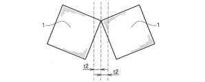
図2は、第1実施形態に係る半導体素子の実装方法の手順を示すフローチャートである。図3Aは、第1実施形態に係る半導体素子の実装方法において、半導体素子を載置する工程で、伸縮性フィルムを固定器具に取り付け、固定器具で伸縮性フィルムを伸張させた状態を模式的に示す平面図である。図3Bは、第1実施形態に係る半導体素子の実装方法において、半導体素子を載置する工程で、伸縮性フィルムに半導体素子を載置した状態を模式的に示す平面図である。図3Cは、第1実施形態に係る半導体素子の実装方法において、伸縮性フィルムの伸張状態を解除する工程を模式的に示す平面図である。図4は、従来技術における、半導体素子を支持基板に実装する際に半導体素子同士が接触する状態を説明する模式的な平面図である。図5Aは、従来技術における、半導体素子を支持基板に実装する際の実装精度について説明する模式的な平面図である。図5Bは、従来技術における、半導体素子を支持基板に実装する際のθ回転について説明する模式的な平面図である。図5Cは、従来技術における、半導体素子を支持基板に実装する際の必要クリアランスについて説明する模式的な平面図である。
[Semiconductor element mounting method]
Next, an example of a method for mounting a semiconductor element will be described.
FIG. 2 is a flowchart showing the steps of the semiconductor device mounting method according to the first embodiment. FIG. 3A schematically shows a state in which a stretchable film is attached to a fixing device and the stretchable film is stretched by the fixing device in the step of mounting a semiconductor device in the semiconductor device mounting method according to the first embodiment. FIG. FIG. 3B is a plan view schematically showing a state in which a semiconductor element is placed on a stretchable film in the step of placing the semiconductor element in the semiconductor element mounting method according to the first embodiment. FIG. 3C is a plan view schematically showing a step of releasing the stretched state of the stretchable film in the semiconductor element mounting method according to the first embodiment. FIG. 4 is a schematic plan view illustrating a state in which semiconductor elements come into contact with each other when semiconductor elements are mounted on a support substrate in the prior art. FIG. 5A is a schematic plan view illustrating the mounting accuracy when mounting a semiconductor element on a support substrate in the prior art. FIG. 5B is a schematic plan view illustrating θ rotation when mounting a semiconductor element on a support substrate in the prior art. FIG. 5C is a schematic plan view illustrating the required clearance when mounting a semiconductor element on a support substrate in the prior art.
半導体素子の実装方法は、伸縮性フィルム20を弾性力に抗して伸張させ、伸張状態の伸縮性フィルム20の予め設定された領域に複数の半導体素子1を離隔して載置する、半導体素子を載置する工程S101と、伸縮性フィルム20の弾性力によって伸張状態を解除する、伸張状態を解除する工程S102と、を含み、この順に行う。そして、半導体素子の実装方法は、半導体素子1を載置した直後の半導体素子1同士の間隔(d1)より、伸縮性フィルム20の伸張状態を解除した後の半導体素子1同士の間隔(d2)の方を狭くして、半導体素子1同士の間隔(d2)を実装間隔とする。
以下、各工程について説明する。なお、各部材の材質や配置等については、前記した半導体装置100の説明で述べた通りであるので、ここでは、適宜、説明を省略する。
A method for mounting a semiconductor device is to stretch a
Each step will be explained below. Note that the materials, arrangement, etc. of each member are as described in the description of the
(半導体素子を載置する工程)
半導体素子を載置する工程S101は、伸縮性フィルム20を弾性力に抗して伸張させ、伸張状態の伸縮性フィルム20の予め設定された領域に複数の半導体素子1を離隔して載置する工程である。
この工程S101では、伸縮性フィルム20を固定器具30に取り付け、固定器具30で伸縮性フィルム20を伸張させる。又は、伸縮性フィルム20を伸張させ、伸縮性フィルム20を伸張させた伸張状態で固定器具30に固定する。ここでは、固定器具30で伸縮性フィルム20を伸張させた状態であるものとする。
また、この工程S101では、X方向に沿った一方(Xプラス方向)と他方(Xマイナス方向)との2方向と、X方向と直交するY方向に沿った一方(Yプラス方向)と他方(Yマイナス方向)との2方向と、の4方向に伸縮性フィルム20を伸張させる。
(Step of placing semiconductor element)
In the step S101 of placing semiconductor elements, the
In this step S101, the
In addition, in this step S101, two directions, one (X-plus direction) and the other (X-minus direction) along the X direction, and one (Y-plus direction) and the other (Y-plus direction) along the Y direction orthogonal to the X direction ( The
伸縮性フィルム20の伸張は、4方向の全てで同じ伸び率となるように行うことが好ましい。全て同じ伸び率とすることで、伸張状態での半導体素子1の実装間隔や、伸張状態を解除した後の半導体素子1の実装間隔を調整し易くなり、半導体素子1を実装し易くなる。伸び率は、伸張状態での半導体素子1の実装間隔や、伸張状態を解除した後の半導体素子1の実装間隔等を考慮して適宜設定すればよい。
また、半導体装置100における半導体素子1同士の間隔が200μm以下である場合、伸縮性フィルム20を伸張させた際の相対する2方向の伸張幅は、50μm以上500μm以下が好ましい。伸張幅が50μm以上であれば、伸縮性フィルム20に半導体素子1を載置し易くなる。一方、伸張幅が500μm以下であれば、半導体素子1の実装部に歪みが生じることを抑制することができる。伸張幅は、より好ましくは、50μm以上200μm以下である。
It is preferable to stretch the
Further, when the distance between the
伸縮性フィルム20としては、所望のクリアランス(半導体素子1同士の間隔)を確保できるだけの伸び率があり、半導体素子1を問題なく実装できるものであればよい。伸縮性フィルム20の材料としては、例えば、UVテープ、各種プラスチック、ゴム等が挙げられる。伸縮性フィルム20の厚さは、例えば、10μm以上500μm以下が好ましく、20μm以上200μm以下であることが更に好ましい。伸縮性フィルム20の伸び率は700%以下が好ましく、500%以下が更に好ましく、300%以下が特に好ましい。伸縮性フィルム20の伸び率が500%を超えるものを用いることにより、半導体素子1を高密度に配置することができる。また、伸縮性フィルム20の伸び率を300%以下に抑えることにより、伸縮性フィルム20を配線等に使用することができたり、伸縮性フィルム20の破断を抑制したりすることができる。
固定器具30としては、従来公知の固定器具30を使用することができる。
The
As the fixing
この工程S101では、半導体素子1の4つを1組として、各組の半導体素子1を行列方向に載置する。そして、4つの半導体素子1を含む各組を一列として、行列方向に、4行×4列で配置する。ここでは、16組が行列方向に配置され、64個の半導体素子1が載置されている。
また、この工程S101では、例えば、各組の半導体素子1同士の間隔が50μm以上500μm以下となるように半導体素子1を載置する。
ここでは、半導体素子1を電極11,12が伸縮性フィルム20に対向するように、半導体素子1を伸縮性フィルム20に載置する。
In this step S101, each set of four
Further, in this step S101, the
Here, the
(伸張状態を解除する工程)
伸張状態を解除する工程S102は、伸縮性フィルム20の弾性力によって伸張状態を解除する工程である。この工程S102では、伸縮性フィルム20を伸張状態としている固定器具30から外し、伸縮性フィルム20の弾性力によって伸張状態を解除する。
この工程S102では、半導体素子1を載置した直後の半導体素子1同士の間隔(d1)より、伸縮性フィルム20の伸張状態を解除した後の半導体素子1同士の間隔(d2)の方を狭くして、半導体素子1同士の間隔(d2)を実装間隔とする。ここでは、各組の4つの半導体素子1同士の間隔を狭くして半導体素子1の実装間隔とする。また、伸張状態を保持している状態において、4つの半導体素子1を1組として、1組内の隣り合う半導体素子1の間隔より、1組の半導体素子1が隣り合う組の半導体素子1の間隔の方を広くすることにより、伸張状態を解除した際に、4つの半導体素子1を1組とすることもできる。
また、この工程S102では、伸縮性フィルム20の伸張状態を解除した後の各組の半導体素子1の実装間隔を0μm以上50μm以下とする。
(Process of releasing the stretched state)
The step S102 of releasing the stretched state is a step of releasing the stretched state by the elastic force of the
In this step S102, the interval (d2) between the
Further, in this step S102, the mounting interval between the
以上のように、本実施形態の半導体素子1の実装方法によれば、半導体素子1の高密度化ができる。ここで、従来技術の場合、複数の半導体素子1(チップ)を基板に実装する際に、クリアランスがないと半導体素子1がθ回転すること等で、半導体素子1同士が縦方向で接触してしまい、半導体素子1を実装できない場合がある(図4参照)。そこで、従来技術では、半導体素子1を実装する場合、「実装精度+θ回転分のクリアランス」が必要となり、例えば、以下の条件の場合、必要クリアランスは、66μm以上160μm以下となる(図5A~図5C参照)。
As described above, according to the mounting method of the
「条件」
・想定チップサイズ:一辺の長さが100μm以上2mm以下の正四角形
・(一般的な)実装精度(t1):±30μm 計60μm
・(一般的な)θ回転:±3°
・2mmチップが3°回転した場合の回転によるズレ量(t2):約50μm
・100μmチップが3°回転した場合の回転によるズレ量(t2):約3μm
・2mmチップの場合の必要クリアランス(T):30×2+50×2=160μm
・100μmチップの場合の必要クリアランス(T):30×2+3×2=66μm
"conditions"
・Assumed chip size: Regular square with side length of 100 μm or more and 2 mm or less ・(General) mounting accuracy (t1): ±30 μm, total 60 μm
・(General) θ rotation: ±3°
・Amount of deviation due to rotation (t2) when a 2mm chip is rotated 3 degrees: approximately 50μm
・Amount of deviation due to rotation (t2) when a 100 μm chip is rotated by 3 degrees: Approximately 3 μm
・Required clearance (T) for 2mm chip: 30 x 2 + 50 x 2 = 160 μm
・Required clearance (T) for 100μm chip: 30×2+3×2=66μm
これに対し、本実施形態では、伸張状態の伸縮性フィルム20の予め設定された領域に複数の半導体素子1を離隔して載置するため、半導体素子1の実装時に半導体素子1同士が接触することがない。また、仮に、伸縮性フィルム20の伸張状態を解除した際に半導体素子1同士が接触したとしても、伸縮性フィルム20の伸縮が応力を吸収し、半導体素子1の損傷が防止される。そのため、従来よりも、狭い実装間隔を設定することができる。なお、伸縮性フィルム20の伸張状態を解除した際、多少、伸縮性フィルム20によれが生じた場合でも、後述するように、半導体装置100の製造方法の工程で伸縮性フィルム20を剥がすので問題は生じない。
On the other hand, in the present embodiment, since a plurality of
[半導体装置の製造方法]
次に、半導体装置の製造方法の一例について説明する。
図6は、第1実施形態に係る半導体装置の製造方法の手順を示すフローチャートである。図7Aは、第1実施形態に係る半導体装置の製造方法において、半導体素子を支持基板に載置する工程及びフィルムを剥がして電極を露出させる工程を模式的に示す平面図である。図7Bは、第1実施形態に係る半導体装置の製造方法において、半導体素子を被覆部材で被覆する工程を模式的に示す平面図である。図7Cは、第1実施形態に係る半導体装置の製造方法において、半導体素子を被覆部材で被覆する工程を模式的に示す断面図であり、図7BのVIIC-VIIC線における断面図である。図7Dは、第1実施形態に係る半導体装置の製造方法において、研磨して電極を露出させる工程を模式的に示す平面図である。図7Eは、第1実施形態に係る半導体装置の製造方法において、研磨して電極を露出させる工程を模式的に示す断面図であり、図7DのVIIE-VIIE線における断面図である。図7Fは、第1実施形態に係る半導体装置の製造方法において、支持基板を剥がす工程及び半導体素子を個片化する工程を模式的に示す平面図である。図7Gは、第1実施形態に係る半導体装置の製造方法において、支持基板を剥がす工程及び半導体素子を個片化する工程を模式的に示す断面図であり、図7FのVIIG-VIIG線における断面図である。
[Method for manufacturing semiconductor device]
Next, an example of a method for manufacturing a semiconductor device will be described.
FIG. 6 is a flowchart showing the steps of the method for manufacturing a semiconductor device according to the first embodiment. FIG. 7A is a plan view schematically showing a step of mounting a semiconductor element on a support substrate and a step of peeling off a film to expose an electrode in the method for manufacturing a semiconductor device according to the first embodiment. FIG. 7B is a plan view schematically showing a step of covering a semiconductor element with a covering member in the method for manufacturing a semiconductor device according to the first embodiment. FIG. 7C is a cross-sectional view schematically showing a step of covering a semiconductor element with a covering member in the method for manufacturing a semiconductor device according to the first embodiment, and is a cross-sectional view taken along line VIIC-VIIC in FIG. 7B. FIG. 7D is a plan view schematically showing a step of polishing to expose an electrode in the method of manufacturing a semiconductor device according to the first embodiment. FIG. 7E is a cross-sectional view schematically showing a step of polishing to expose an electrode in the method for manufacturing a semiconductor device according to the first embodiment, and is a cross-sectional view taken along the line VIIE-VIIE in FIG. 7D. FIG. 7F is a plan view schematically showing the step of peeling off the support substrate and the step of dividing the semiconductor element into pieces in the method for manufacturing a semiconductor device according to the first embodiment. FIG. 7G is a cross-sectional view schematically showing the step of peeling off the support substrate and the step of dividing the semiconductor element into pieces in the method for manufacturing a semiconductor device according to the first embodiment, and is a cross-sectional view taken along the line VIIG-VIIG in FIG. 7F. It is a diagram.
半導体装置の製造方法は、前記記載の半導体素子の実装方法を行った後、電極11,12と反対の面が支持基板21に対向するように、半導体素子1を支持基板21に載置する、支持基板に載置する工程S201と、伸縮性フィルム20を剥がし、電極11,12を露出させる、フィルムを剥がして電極を露出させる工程S202と、電極11,12を覆うように、半導体素子1を被覆部材2で被覆する、被覆部材で被覆する工程S203と、被覆部材2を研磨して、電極11,12を露出させる、研磨して電極を露出させる工程S204と、支持基板を剥がす工程S205と、半導体素子1を個片化する、個片化する工程S206と、を含み、この順に行う。
以下、各工程について説明する。なお、各部材の材質や配置等については、前記した半導体装置100の説明で述べた通りであるので、ここでは、適宜、説明を省略する。
The method for manufacturing a semiconductor device includes performing the above-described semiconductor element mounting method, and then placing the
Each step will be explained below. Note that the materials, arrangement, etc. of each member are as described in the description of the
(支持基板に載置する工程)
支持基板に載置する工程S201は、第1実施形態に係る半導体素子の実装方法で実装された半導体素子1を、電極11,12と反対の面が支持基板21に対向するように、半導体素子1を支持基板21に載置する工程である。
この工程S201では、まず、伸縮性フィルム20に半導体素子1が載置された状態で、半導体素子1の波長変換部材3が支持基板21に接着するように、半導体素子1を支持基板21に載置する。
支持基板21としては、例えば、ポリイミドフィルム、PETフィルム等が挙げられる。
支持基板21の厚さは、例えば、5μm以上300μm以下が好ましく、10μm以上150μm以下が更に好ましい。
(Step of placing on support substrate)
In step S201 of mounting the
In this step S201, first, with the
Examples of the
The thickness of the
(フィルムを剥がして電極を露出させる工程)
フィルムを剥がして電極を露出させる工程S202は、伸縮性フィルム20を剥がし、電極11,12の下面を露出させる工程である。
(Step of peeling off the film to expose the electrodes)
Step S202 of peeling off the film to expose the electrodes is a step of peeling off the
(被覆部材で被覆する工程)
被覆部材で被覆する工程S203は、電極11,12を覆うように、半導体素子1を被覆部材2で被覆する工程である。
この工程S203では、電極11,12を含めた半導体素子1の全部を被覆部材2で被覆する。ここでは、被覆部材2は、電極11,12の上面が被覆されるように設けられている。
半導体素子1の被覆は、例えば、固定された支持基板21の上側において、支持基板21に対して上下方向あるいは水平方向等に移動(可動)させることができる吐出装置(ディスペンサー)を用いて行うことができる。半導体素子1の被覆は、吐出装置を用いて、被覆部材2を構成する樹脂等を支持基板21上に充填することにより行うことができる。
また、圧縮成形法、トランスファー成形法等によって被覆することも可能である。
(Process of covering with covering member)
The step S203 of covering with the covering member is a step of covering the
In this step S203, the
The coating of the
Moreover, it is also possible to cover by a compression molding method, a transfer molding method, or the like.
(研磨して電極を露出させる工程)
研磨して電極を露出させる工程S204は、被覆部材2を研磨して、電極11,12を露出させる工程である。
この工程S204では、電極11,12側から、被覆部材2の表面を電極11,12が露出するまで研磨する。
(Process of polishing to expose the electrode)
The step S204 of polishing to expose the electrodes is a step of polishing the covering
In this step S204, the surface of the covering
(支持基板を剥がす工程)
支持基板を剥がす工程S205は、被覆部材2を研磨して電極11,12を露出させた後、支持基板21を剥がす工程である。
(Step of peeling off the support substrate)
Step S205 of peeling off the support substrate is a step of polishing the covering
(個片化する工程)
個片化する工程S206は、半導体素子1を個片化する工程である。
この工程S206では、個々の半導体装置100となるように、切断線15に沿って所定の領域で電極11,12を露出させた成型体を切断する。切断は、例えば、ブレードで切断するダイシング方法等、従来公知の方法により行うことができる。
これにより、4つの半導体素子1を備える半導体装置100が得られる。
(Individualization process)
The step S206 of singulating is a step of dividing the
In this step S206, the molded body with the
As a result, a
<第2実施形態>
次に、第2実施形態に係る半導体装置の製造方法の一例について説明する。なお、第2実施形態に係る半導体素子の実装方法は、第1実施形態に係る半導体素子の実装方法と同様であるので、説明を省略する。
図8Aは、第2実施形態に係る半導体装置の製造方法の手順を示すフローチャートである。
第2実施形態に係る半導体装置の製造方法は、第1実施形態に係る半導体装置の製造方法で説明した、支持基板に載置する工程S201と、フィルムを剥がして電極を露出させる工程S202と、被覆部材で被覆する工程S203と、研磨して電極を露出させる工程S204と、を含み、この順に行うものである。すなわち、図7Cに示すように、支持基板22を有し、個片化していないものを半導体装置としたものである。
<Second embodiment>
Next, an example of a method for manufacturing a semiconductor device according to the second embodiment will be described. Note that the method for mounting a semiconductor element according to the second embodiment is the same as the method for mounting a semiconductor element according to the first embodiment, so a description thereof will be omitted.
FIG. 8A is a flowchart showing the steps of the method for manufacturing a semiconductor device according to the second embodiment.
The method for manufacturing a semiconductor device according to the second embodiment includes the step S201 of mounting the semiconductor device on a support substrate, the step S202 of peeling off the film to expose the electrodes, as described in the method for manufacturing a semiconductor device according to the first embodiment. The process includes a step S203 of covering with a covering member and a step S204 of polishing to expose the electrode, which are performed in this order. That is, as shown in FIG. 7C, a semiconductor device is one that has a support substrate 22 and is not separated into individual pieces.
<第3実施形態>
次に、第3実施形態に係る半導体装置の製造方法の一例について説明する。なお、第3実施形態に係る半導体素子の実装方法は、第1実施形態に係る半導体素子の実装方法と同様であるので、説明を省略する。
図8Bは、第3実施形態に係る半導体装置の製造方法の手順を示すフローチャートである。
第3実施形態に係る半導体装置の製造方法は、第1実施形態に係る半導体装置の製造方法で説明した、支持基板に載置する工程S201と、フィルムを剥がして電極を露出させる工程S202と、を含み、この順に行うものである。すなわち、図7Aに示すように、支持基板21を有し、被覆部材2を有さず、個片化していないものを半導体装置としたものである。
<Third embodiment>
Next, an example of a method for manufacturing a semiconductor device according to the third embodiment will be described. Note that the method for mounting a semiconductor element according to the third embodiment is the same as the method for mounting a semiconductor element according to the first embodiment, so a description thereof will be omitted.
FIG. 8B is a flowchart showing the steps of the method for manufacturing a semiconductor device according to the third embodiment.
The method for manufacturing a semiconductor device according to the third embodiment includes the step S201 of placing the semiconductor device on a support substrate, the step S202 of peeling off the film to expose the electrodes, as described in the method for manufacturing a semiconductor device according to the first embodiment. and should be performed in this order. That is, as shown in FIG. 7A, a semiconductor device is one that has a supporting
<第4実施形態>
次に、第4実施形態に係る半導体装置の製造方法の一例について説明する。なお、第4実施形態に係る半導体素子の実装方法は、第1実施形態に係る半導体素子の実装方法と同様であるので、説明を省略する。
図9は、第4実施形態に係る半導体装置の製造方法の手順を示すフローチャートである。図10Aは、第4実施形態に係る半導体装置の製造方法において、半導体素子を被覆部材で被覆する工程を模式的に示す平面図である。図10Bは、第4実施形態に係る半導体装置の製造方法において、半導体素子を被覆部材で被覆する工程を模式的に示す断面図であり、図10AのXB-XB線における断面図である。図10Cは、第4実施形態に係る半導体装置の製造方法において、フィルムを剥がして電極を露出させる工程を模式的に示す平面図である。図10Dは、第4実施形態に係る半導体装置の製造方法において、フィルムを剥がして電極を露出させる工程を模式的に示す断面図であり、図10CのXD-XD線における断面図である。図10Eは、第4実施形態に係る半導体装置の製造方法において、半導体素子を個片化する工程を模式的に示す平面図である。
<Fourth embodiment>
Next, an example of a method for manufacturing a semiconductor device according to the fourth embodiment will be described. Note that the method for mounting a semiconductor element according to the fourth embodiment is the same as the method for mounting a semiconductor element according to the first embodiment, so a description thereof will be omitted.
FIG. 9 is a flowchart showing the steps of a method for manufacturing a semiconductor device according to the fourth embodiment. FIG. 10A is a plan view schematically showing a step of covering a semiconductor element with a covering member in a method of manufacturing a semiconductor device according to a fourth embodiment. FIG. 10B is a cross-sectional view schematically showing a step of covering a semiconductor element with a covering member in the method for manufacturing a semiconductor device according to the fourth embodiment, and is a cross-sectional view taken along the line XB-XB in FIG. 10A. FIG. 10C is a plan view schematically showing a step of peeling off a film to expose an electrode in the method for manufacturing a semiconductor device according to the fourth embodiment. FIG. 10D is a cross-sectional view schematically showing a step of peeling off a film to expose an electrode in the method for manufacturing a semiconductor device according to the fourth embodiment, and is a cross-sectional view taken along the line XD-XD in FIG. 10C. FIG. 10E is a plan view schematically showing a step of dividing a semiconductor element into pieces in the method for manufacturing a semiconductor device according to the fourth embodiment.
第4実施形態に係る半導体装置の製造方法は、第1実施形態に係る半導体素子の実装方法を行った後、半導体素子1を被覆部材2で被覆する、被覆部材で被覆する工程S301と、伸縮性フィルム20を剥がし、電極11,12を露出させる、フィルムを剥がして電極を露出させる工程S302と、半導体素子1を個片化する、個片化する工程S303と、を含み、この順に行う。
以下、各工程について説明する。なお、各部材の材質や配置等については、前記した半導体装置100の説明で述べた通りであるので、ここでは、適宜、説明を省略する。
The method for manufacturing a semiconductor device according to the fourth embodiment includes a step S301 of covering the
Each step will be explained below. Note that the materials, arrangement, etc. of each member are as described in the description of the
(被覆部材で被覆する工程)
被覆部材で被覆する工程S301は、半導体素子1を被覆部材2で被覆する工程である。
この工程S301では、伸縮性フィルム20上に、半導体素子1の側面を被覆するように、被覆部材2を配置する。半導体素子1の被覆は、第1実施形態に係る半導体装置の製造方法に準じて行えばよい。なお、波長変換部材3の上面が被覆部材2で被覆された場合は、研磨等により被覆部材2を除去して、波長変換部材3の上面を露出させればよい。
(Process of covering with covering member)
The step S301 of covering with the covering member is a step of covering the
In this step S301, the covering
(フィルムを剥がして電極を露出させる工程)
フィルムを剥がして電極を露出させる工程S302は、伸縮性フィルム20を剥がし、電極11,12の下面を露出させる工程である。なお、図10C、図10Dでは、電極11,12側を上面としている。
(Step of peeling off the film to expose the electrodes)
Step S302 of peeling off the film to expose the electrodes is a step of peeling off the
(個片化する工程)
個片化する工程S303は、半導体素子1を個片化する工程である。半導体素子1を個片化は、第1実施形態に係る半導体装置の製造方法に準じて行えばよい。
これにより、4つの半導体素子1を備える半導体装置100が得られる。
(Individualization process)
The singulation process S303 is a process of singulating the
As a result, a
<第5実施形態>
次に、第5実施形態に係る半導体装置の製造方法の一例について説明する。なお、第5実施形態に係る半導体素子の実装方法は、第1実施形態に係る半導体素子の実装方法と同様であるので、説明を省略する。
図11は、第5実施形態に係る半導体装置の製造方法の手順を示すフローチャートである。図12Aは、第5実施形態に係る半導体装置の製造方法において、半導体素子を被覆部材で被覆する工程を模式的に示す平面図である。図12Bは、第5実施形態に係る半導体装置の製造方法において、半導体素子を個片化する工程を模式的に示す平面図である。図12Cは、第5実施形態に係る半導体装置の製造方法において、フィルムを剥がして電極を露出させる工程を模式的に示す平面図である。
<Fifth embodiment>
Next, an example of a method for manufacturing a semiconductor device according to a fifth embodiment will be described. Note that the method for mounting a semiconductor element according to the fifth embodiment is the same as the method for mounting a semiconductor element according to the first embodiment, so a description thereof will be omitted.
FIG. 11 is a flowchart showing the steps of the method for manufacturing a semiconductor device according to the fifth embodiment. FIG. 12A is a plan view schematically showing a step of covering a semiconductor element with a covering member in the method for manufacturing a semiconductor device according to the fifth embodiment. FIG. 12B is a plan view schematically showing a step of dividing a semiconductor element into pieces in the method for manufacturing a semiconductor device according to the fifth embodiment. FIG. 12C is a plan view schematically showing a step of peeling off a film to expose an electrode in the method for manufacturing a semiconductor device according to the fifth embodiment.
第5実施形態に係る半導体装置の製造方法は、第1実施形態に係る半導体素子の実装方法を行った後、半導体素子1を被覆部材2で被覆する、被覆部材で被覆する工程S301aと、半導体素子1を個片化する、個片化する工程S302aと、伸縮性フィルム20を剥がし、電極11,12を露出させる、フィルムを剥がして電極を露出させる工程S303aと、を含み、この順に行う。
第5実施形態に係る半導体装置の製造方法は、第4実施形態に係る半導体装置の製造方法において、フィルムを剥がして電極を露出させる工程S302の前に、個片化する工程S303を行うものである。その他については、第4実施形態に係る半導体装置の製造方法と同様である。
なお、個片化する工程S302aでは、伸縮性フィルム20は切断されてもよく、切断されなくてもよい。
The method for manufacturing a semiconductor device according to the fifth embodiment includes a step S301a of covering the
The method for manufacturing a semiconductor device according to the fifth embodiment is such that, in the method for manufacturing a semiconductor device according to the fourth embodiment, the step S303 of singulating is performed before the step S302 of peeling off the film to expose the electrodes. be. Other aspects are the same as the method for manufacturing a semiconductor device according to the fourth embodiment.
In addition, in step S302a of dividing into pieces, the
<第6実施形態>
次に、第6実施形態に係る半導体装置の製造方法の一例について説明する。なお、第6実施形態に係る半導体素子の実装方法は、第1実施形態に係る半導体素子の実装方法と同様であるので、説明を省略する。
図13は、第6実施形態に係る半導体装置の製造方法の手順を示すフローチャートである。
第6実施形態に係る半導体装置の製造方法は、第4実施形態に係る半導体装置の製造方法で説明した、半導体素子1を被覆部材2で被覆する、被覆部材で被覆する工程S301と、伸縮性フィルム20を剥がし、電極11,12を露出させる、フィルムを剥がして電極を露出させる工程S302と、を含み、この順に行うものである。すなわち、図10Bに示すように、個片化していないものを半導体装置としたものである。
<Sixth embodiment>
Next, an example of a method for manufacturing a semiconductor device according to a sixth embodiment will be described. Note that the method for mounting a semiconductor element according to the sixth embodiment is the same as the method for mounting a semiconductor element according to the first embodiment, so a description thereof will be omitted.
FIG. 13 is a flowchart showing the steps of a method for manufacturing a semiconductor device according to the sixth embodiment.
The method for manufacturing a semiconductor device according to the sixth embodiment includes steps S301 of covering the
<第7実施形態>
次に、第7実施形態に係る半導体素子の実装方法及び半導体装置の製造方法の一例について説明する。
[半導体素子の実装方法]
図14は、第7実施形態に係る半導体素子の実装方法の手順を示すフローチャートである。図15Aは、第7実施形態に係る半導体素子の実装方法において、半導体素子を載置する工程で、伸縮性フィルムに半導体素子を載置した状態を模式的に示す平面図である。図15Bは、第7実施形態に係る半導体素子の実装方法において、伸縮性フィルムの伸張状態を解除する工程を模式的に示す平面図である。
<Seventh embodiment>
Next, an example of a semiconductor element mounting method and a semiconductor device manufacturing method according to the seventh embodiment will be described.
[Semiconductor element mounting method]
FIG. 14 is a flowchart showing the steps of the semiconductor device mounting method according to the seventh embodiment. FIG. 15A is a plan view schematically showing a state in which a semiconductor element is placed on a stretchable film in the step of placing the semiconductor element in the semiconductor element mounting method according to the seventh embodiment. FIG. 15B is a plan view schematically showing a step of releasing the stretched state of the stretchable film in the semiconductor element mounting method according to the seventh embodiment.
第7実施形態に係る半導体素子の実装方法は、電極11,12を有する面とは反対の面が伸縮性フィルム20に対向するように、半導体素子1を伸縮性フィルム20に載置する、半導体素子を載置する工程S101aと、伸縮性フィルム20の弾性力によって伸張状態を解除する、伸張状態を解除する工程S102aと、を含み、この順に行う。
第7実施形態に係る半導体素子の実装方法では、半導体素子1の波長変換部材3が伸縮性フィルム20に接着するように、半導体素子1を伸縮性フィルム20に載置する。それ以外の事項については、第1実施形態の半導体素子の実装方法と同様である。
The semiconductor device mounting method according to the seventh embodiment includes placing the
In the semiconductor element mounting method according to the seventh embodiment, the
[半導体装置の製造方法]
図16は、第7実施形態に係る半導体装置の製造方法の手順を示すフローチャートである。図17Aは、第7実施形態に係る半導体素子の実装方法において、半導体素子を支持基板に載置する工程及び伸縮性フィルムを剥がす工程を模式的に示す平面図である。図17Bは、第7実施形態に係る半導体素子の実装方法において、半導体素子を被覆部材で被覆する工程を模式的に示す平面図である。図17Cは、第7実施形態に係る半導体素子の実装方法において、支持基板を剥がす工程を模式的に示す平面図である。図17Dは、第7実施形態に係る半導体素子の実装方法において、支持基板を個片化する工程を模式的に示す平面図である。
[Method for manufacturing semiconductor device]
FIG. 16 is a flowchart showing the steps of the method for manufacturing a semiconductor device according to the seventh embodiment. FIG. 17A is a plan view schematically showing a step of mounting a semiconductor device on a support substrate and a step of peeling off a stretchable film in the semiconductor device mounting method according to the seventh embodiment. FIG. 17B is a plan view schematically showing a step of covering a semiconductor element with a covering member in the semiconductor element mounting method according to the seventh embodiment. FIG. 17C is a plan view schematically showing a step of peeling off the support substrate in the semiconductor element mounting method according to the seventh embodiment. FIG. 17D is a plan view schematically showing the step of dividing the support substrate into pieces in the semiconductor element mounting method according to the seventh embodiment.
半導体装置の製造方法は、第7実施形態に係る半導体素子の実装方法を行った後、電極11,12が支持基板21に対向するように、半導体素子1を支持基板21に載置する、支持基板に載置する工程S401と、伸縮性フィルムを剥がす工程S402と、半導体素子1を被覆部材2で被覆する、被覆部材で被覆する工程S403と、支持基板を剥がす工程S404と、半導体素子1を個片化する、個片化する工程S405と、を含み、この順に行う。
The method for manufacturing a semiconductor device includes a support process in which, after performing the semiconductor element mounting method according to the seventh embodiment, the
半導体装置の製造方法は、支持基板に載置する工程S401において、電極11,12が下面となるように半導体素子1を支持基板21に載置する。すなわち、波長変換部材3が上面となるように半導体素子1を支持基板21に載置する。次に、伸縮性フィルムを剥がす工程S402において、伸縮性フィルム20を剥がして波長変換部材3を露出させる。次に、被覆部材で被覆する工程S403において、支持基板21上に、半導体素子1の側面を被覆するように、被覆部材2を配置する。なお、波長変換部材3の上面が被覆部材2で被覆された場合は、研磨等により被覆部材2を除去して、波長変換部材3の上面を露出させればよい。次に、支持基板を剥がす工程S404において、波長変換部材3を露出させた成型体を支持基板21から剥がす。次に、個片化する工程S405において、個々の半導体装置100となるように、切断線15に沿って所定の領域で成型体を切断する。それ以外の事項については、第1実施形態に係る半導体装置の製造方法と同様である。
これにより、4つの半導体素子1を備える半導体装置100が得られる。
In the method for manufacturing a semiconductor device, in step S401 of placing the
As a result, a
<第8実施形態>
次に、第8実施形態に係る半導体装置の製造方法の一例について説明する。なお、第8実施形態に係る半導体素子の実装方法は、第7実施形態に係る半導体素子の実装方法と同様であるので、説明を省略する。
図18は、第8実施形態に係る半導体装置の製造方法の手順を示すフローチャートである。図19は、第8実施形態に係る半導体素子の実装方法において、半導体素子を個片化する工程を模式的に示す平面図である。
<Eighth embodiment>
Next, an example of a method for manufacturing a semiconductor device according to the eighth embodiment will be described. Note that the method for mounting a semiconductor element according to the eighth embodiment is the same as the method for mounting a semiconductor element according to the seventh embodiment, so a description thereof will be omitted.
FIG. 18 is a flowchart showing the steps of a method for manufacturing a semiconductor device according to the eighth embodiment. FIG. 19 is a plan view schematically showing a step of dividing a semiconductor element into pieces in the semiconductor element mounting method according to the eighth embodiment.
第8実施形態に係る半導体装置の製造方法は、第7実施形態に係る半導体装置の製造方法で説明した、電極11,12が支持基板21に対向するように、半導体素子1を支持基板21に載置する、支持基板に載置する工程S401と、伸縮性フィルムを剥がす工程S402と、半導体素子1を被覆部材2で被覆する、被覆部材で被覆する工程S403と、半導体素子を個片化する、個片化する工程S405と、を含み、この順に行うものである。
In the method for manufacturing a semiconductor device according to the eighth embodiment, the
第8実施形態に係る半導体装置の製造方法は、支持基板を剥がす工程S404を行わず、支持基板21上で半導体素子1を個片化する。なお、個片化する工程S405では、支持基板21は切断されてもよく、切断されなくてもよい。また、個片化する工程S405の後に、支持基板21を剥がしてもよい。
In the method for manufacturing a semiconductor device according to the eighth embodiment, the
<第9実施形態>
次に、第9実施形態に係る半導体装置の製造方法の一例について説明する。なお、第9実施形態に係る半導体素子の実装方法は、第7実施形態に係る半導体素子の実装方法と同様であるので、説明を省略する。
図20Aは、第9実施形態に係る半導体装置の製造方法の手順を示すフローチャートである。
半導体装置の製造方法は、第7実施形態に係る半導体素子の実装方法を行った後、電極11,12が支持基板21に対向するように、半導体素子1を支持基板21に載置する、支持基板に載置する工程S501と、支持基板21と伸縮性フィルム20との間に、半導体素子1の側面を被覆する被覆部材2を配置する、被覆部材を配置する工程S502と、支持基板を剥がす工程S503と、伸縮性フィルムを剥がす工程S504と、半導体素子1を個片化する、個片化する工程S505と、を含み、この順に行う。
<Ninth embodiment>
Next, an example of a method for manufacturing a semiconductor device according to a ninth embodiment will be described. Note that the method for mounting a semiconductor element according to the ninth embodiment is the same as the method for mounting a semiconductor element according to the seventh embodiment, so a description thereof will be omitted.
FIG. 20A is a flowchart showing the steps of the method for manufacturing a semiconductor device according to the ninth embodiment.
The method for manufacturing a semiconductor device includes a support process in which, after performing the semiconductor element mounting method according to the seventh embodiment, the
被覆部材を配置する工程S502では、支持基板21と伸縮性フィルム20との間に、半導体素子1の側面を被覆するように、被覆部材2を配置する。半導体素子1の被覆は、第1実施形態に係る半導体装置の製造方法に準じて行えばよく、この際、被覆部材2は、支持基板21と伸縮性フィルム20との間に充填すればよい。それ以外の事項については、第7実施形態に係る半導体装置の製造方法と工程順序が異なるだけで、第7実施形態に係る半導体装置の製造方法と同様である。
これにより、4つの半導体素子1を備える半導体装置100が得られる。
In step S502 of arranging the covering member, the covering
As a result, a
<第10実施形態>
次に、第10実施形態に係る半導体装置の製造方法の一例について説明する。なお、第10実施形態に係る半導体素子の実装方法は、第7実施形態に係る半導体素子の実装方法と同様であるので、説明を省略する。
図20Bは、第10実施形態に係る半導体装置の製造方法の手順を示すフローチャートである。
第10実施形態に係る半導体装置の製造方法は、第9実施形態に係る半導体装置の製造方法で説明した、電極11,12が支持基板21に対向するように、半導体素子1を支持基板21に載置する、支持基板に載置する工程S501と、支持基板21と伸縮性フィルム20との間に、半導体素子1の側面を被覆する被覆部材2を配置する、被覆部材を配置する工程S502と、伸縮性フィルムを剥がす工程S504と、半導体素子1を個片化する、個片化する工程S505と、を含み、この順に行うものである。
<Tenth embodiment>
Next, an example of a method for manufacturing a semiconductor device according to a tenth embodiment will be described. Note that the method for mounting a semiconductor element according to the tenth embodiment is the same as the method for mounting a semiconductor element according to the seventh embodiment, so a description thereof will be omitted.
FIG. 20B is a flowchart showing the steps of the method for manufacturing a semiconductor device according to the tenth embodiment.
In the method for manufacturing a semiconductor device according to the tenth embodiment, the
第10実施形態に係る半導体装置の製造方法は、支持基板を剥がす工程S503を行わず、支持基板21上で半導体素子1を個片化する。なお、個片化する工程S505では、支持基板21は切断されてもよく、切断されなくてもよい。また、個片化する工程S505の後に、支持基板21を剥がしてもよい。
In the method for manufacturing a semiconductor device according to the tenth embodiment, the
<第11実施形態>
[半導体装置]
はじめに、半導体装置について説明する。
図21Aは、第11実施形態に係る半導体装置の構成を示す模式的に示す平面図である。図21Bは、第11実施形態に係る半導体装置の構成を示す模式的に示す断面図であり、図1AのXXIB-XXIB線における断面図である。
半導体装置100Aは、半導体素子1と、被覆部材2と、波長変換部材3と、を備えている。
<Eleventh embodiment>
[Semiconductor device]
First, the semiconductor device will be explained.
FIG. 21A is a plan view schematically showing the configuration of a semiconductor device according to the eleventh embodiment. FIG. 21B is a schematic cross-sectional view showing the configuration of the semiconductor device according to the eleventh embodiment, and is a cross-sectional view taken along the line XXIB-XXIB in FIG. 1A.
The
半導体装置100Aは、3つの半導体素子1が、3つの半導体素子1の中心を仮想的に結んだ直線が三角形となるように並べられている。すなわち、半導体装置100は、3つの半導体素子1のち、2つが並列で載置され、残りの1つが、2つの半導体素子1のそれぞれの横側に位置するように載置される。
3つの半導体素子1は、それぞれ、赤色光を発光する第1半導体素子、青色光を発光する第2半導体素子、緑色光を発光する第3半導体素子である。
このような半導体装置100Aによれば、RBGによるフルカラー表示が可能となる。
In the
The three
According to such a
青色(波長430~490nmの光)、緑色(波長495~565nmの光)の半導体素子1としては、窒化物系半導体(InXAlYGa1-X-YN、0≦X、0≦Y、X+Y≦1)、GaP等を用いたものを使用することができる。赤色(波長610~700nmの光)の半導体素子1としては、窒化物系半導体素子の他にもGaAlAs、AlInGaP等を用いることができる。
その他の事項については、第1実施形態に係る半導体装置100と同様である。
As the blue (light with a wavelength of 430 to 490 nm) and green (light with a wavelength of 495 to 565 nm)
Other matters are the same as those of the
[半導体素子の実装方法]
次に、半導体素子の実装方法の一例について説明する。
図22Aは、第11実施形態に係る半導体素子の実装方法において、半導体素子を載置する工程で、伸縮性フィルムを固定器具に取り付け、固定器具で伸縮性フィルムを伸張させた状態を模式的に示す平面図である。図22Bは、第11実施形態に係る半導体素子の実装方法において、半導体素子を載置する工程で、伸縮性フィルムに半導体素子を載置した状態を模式的に示す平面図である。図22Cは、第11実施形態に係る半導体素子の実装方法において、伸縮性フィルムの伸張状態を解除する工程を模式的に示す平面図である。
[Semiconductor element mounting method]
Next, an example of a method for mounting a semiconductor element will be described.
FIG. 22A schematically shows a state in which a stretchable film is attached to a fixing device and the stretchable film is stretched by the fixing device in the step of mounting a semiconductor device in the semiconductor device mounting method according to the eleventh embodiment. FIG. FIG. 22B is a plan view schematically showing a state in which a semiconductor element is placed on a stretchable film in the step of placing the semiconductor element in the semiconductor element mounting method according to the eleventh embodiment. FIG. 22C is a plan view schematically showing a step of releasing the stretched state of the stretchable film in the semiconductor element mounting method according to the eleventh embodiment.
半導体素子の実装方法は、第1実施形態に係る半導体素子の実装方法と同様に、半導体素子を載置する工程S101と、伸張状態を解除する工程S102と、を含み、この順に行う。なお、各部材の材質や配置等については、前記した半導体装置100Aの説明で述べた通りであるので、ここでは、適宜、説明を省略する。
Similar to the semiconductor device mounting method according to the first embodiment, the semiconductor device mounting method includes a step S101 of mounting the semiconductor device and a step S102 of releasing the expanded state, which are performed in this order. Note that the material, arrangement, etc. of each member are as described in the description of the
半導体素子の実装方法は、半導体素子を載置する工程S101において、3つの半導体素子1が伸縮性フィルム20の伸張状態を解除した後に所望の位置になるように、伸縮性フィルム20を伸張させる4方向を調整する。また、半導体素子の実装方法は、半導体素子を載置する工程S101において、半導体素子1の3つを1組として、各組の3つの半導体素子1の中心を仮想的に結んだ直線が三角形となる位置に半導体素子1を載置する。また、半導体素子の実装方法は、伸張状態を解除する工程S102において、各組の3つの半導体素子1同士の間隔を狭くして半導体素子1の実装間隔とする。それ以外の事項については、第1実施形態に係る半導体素子の実装方法と同様である。
The method for mounting semiconductor elements includes, in step S101 of mounting semiconductor elements, stretching the
[半導体装置の製造方法]
第11実施形態に係る半導体装置の製造方法は、半導体素子1の3つを1組とすること以外は、第1~第10実施形態に係る半導体装置の製造方法に準じて行うことができる。
これにより、3つの半導体素子1を備える半導体装置100Aが得られる。
[Method for manufacturing semiconductor device]
The method for manufacturing a semiconductor device according to the eleventh embodiment can be carried out in accordance with the method for manufacturing a semiconductor device according to the first to tenth embodiments, except that three
Thereby, a
<第12実施形態>
[半導体装置]
はじめに、半導体装置について説明する。
図23Aは、第12実施形態に係る半導体装置の構成を示す模式的に示す平面図である。図23Bは、第12実施形態に係る半導体装置の構成を示す模式的に示す断面図であり、図23AのXXIIIB-XXIIIB線における断面図である。
半導体装置100Bは、伸縮性フィルム20と、配線パターン40と、半導体素子1と、波長変換部材3と、を備えている。
伸縮性フィルム20は、第1実施形態の半導体素子の実装方法で説明した伸縮性フィルム20と同様のものを用いることができる。半導体素子1及び波長変換部材3と、は、第1実施形態の半導体装置100で説明した半導体素子1及び波長変換部材3と同様のものを用いることができる。
<Twelfth embodiment>
[Semiconductor device]
First, the semiconductor device will be explained.
FIG. 23A is a plan view schematically showing the configuration of a semiconductor device according to the twelfth embodiment. FIG. 23B is a schematic cross-sectional view showing the configuration of the semiconductor device according to the twelfth embodiment, and is a cross-sectional view taken along line XXIIIB-XXIIIB in FIG. 23A.
The
The
半導体素子1同士の間隔は、0μm以上50μm以下が好ましい。間隔が0μm以上であれば、半導体装置100Bを製造し易くなる。一方、間隔が50μm以下であれば、半導体素子1を更に高密度化することができ、半導体装置100Bを小型化することができる。
The distance between the
(配線パターン)
配線パターン40は、一対の配線パターン41を、半導体素子1を載置する領域が並列するように等間隔で並行に複数形成したものである。
一対の配線パターン41は、2つの直線状の配線42,43が、端部が相対するように所定の間隔を空けて伸縮性フィルム20上に配置されている。配線パターン40は、一対の配線パターン41が並列して4つ設けられている。一対の配線パターン41は、一方の端部に半導体素子1の一方の電極11が接合され、他方の端部に半導体素子1の他方の電極12(図1B参照)が接合されている。これにより、半導体素子1は、一対の配線パターン41上に跨るように、かつ、並列に載置されている。
配線パターン40の材料としては、銅等の金属性の材料、導電性ペースト、ストレッチャブルペースト等を用いることができる。
(wiring pattern)
The
In the pair of
As a material for the
[半導体素子の実装方法及び半導体装置の製造方法]
次に、半導体素子の実装方法及び半導体装置の製造方法の一例について説明する。
図24は、第12実施形態に係る半導体素子の実装方法の手順を示すフローチャートである。図25Aは、第12実施形態に係る半導体素子の実装方法において、配線パターンを形成する工程を模式的に示す平面図である。図25Bは、第12実施形態に係る半導体素子の実装方法において、半導体素子を載置する工程で、伸縮性フィルムを固定器具に取り付け、固定器具で伸縮性フィルムを伸張させた状態を模式的に示す平面図である。図25Cは、図25BのXXVC-XXVC線における断面図である。図25Dは、第12実施形態に係る半導体素子の実装方法において、半導体素子を載置する工程で、伸縮性フィルムに半導体素子を載置した状態を模式的に示す平面図である。図25Eは、第12実施形態に係る半導体素子の実装方法において、伸縮性フィルムの伸張状態を解除する工程を模式的に示す平面図である。
[Semiconductor element mounting method and semiconductor device manufacturing method]
Next, an example of a method for mounting a semiconductor element and a method for manufacturing a semiconductor device will be described.
FIG. 24 is a flowchart showing the steps of the semiconductor device mounting method according to the twelfth embodiment. FIG. 25A is a plan view schematically showing a step of forming a wiring pattern in the semiconductor element mounting method according to the twelfth embodiment. FIG. 25B schematically shows a state in which a stretchable film is attached to a fixing device and the stretchable film is stretched by the fixing device in the step of mounting a semiconductor device in the semiconductor device mounting method according to the twelfth embodiment. FIG. FIG. 25C is a cross-sectional view taken along line XXVC-XXVC in FIG. 25B. FIG. 25D is a plan view schematically showing a state in which a semiconductor element is placed on a stretchable film in the step of placing the semiconductor element in the semiconductor element mounting method according to the twelfth embodiment. FIG. 25E is a plan view schematically showing a step of releasing the stretched state of the stretchable film in the semiconductor element mounting method according to the twelfth embodiment.
第12実施形態では、半導体素子の実装方法により半導体素子が実装された伸縮性フィルムが半導体装置となるため、半導体素子の実装方法と半導体装置の製造方法は同じ工程を経る。以下、代表して半導体素子の実装方法について説明する。 In the twelfth embodiment, the semiconductor device is a stretchable film on which a semiconductor element is mounted using the semiconductor element mounting method, so the semiconductor element mounting method and the semiconductor device manufacturing method go through the same steps. Hereinafter, a method for mounting a semiconductor element will be described as a representative example.
半導体素子の実装方法は、伸縮性フィルム20上に配線パターン40を形成する、配線パターンを形成する工程S601と、伸縮性フィルム20を弾性力に抗して伸張させ、伸張状態の伸縮性フィルム20の予め設定された領域に複数の半導体素子1を離隔して載置する、半導体素子を載置する工程S602と、伸縮性フィルム20の弾性力によって伸張状態を解除する、伸張状態を解除する工程S603と、を含み、この順に行う。配線パターンを形成する工程S601は、半導体素子1を載置する領域を有する一対の配線パターン41を、半導体素子1を載置する領域が並列するように等間隔で複数形成する。
そして、半導体素子の実装方法は、前記半導体素子を載置した直後の前記半導体素子同士の間隔(d1)より、前記伸縮性フィルムの伸張状態を解除した後の前記半導体素子同士の間隔(d2)の方を狭くして、前記半導体素子同士の間隔(d2)を実装間隔とする。
以下、各工程について説明する。なお、各部材の材質や配置等については、前記した半導体装置100Bの説明で述べた通りであるので、ここでは、適宜、説明を省略する。
The method for mounting a semiconductor element includes a step S601 of forming a wiring pattern, in which a
The mounting method for semiconductor elements is based on the distance (d2) between the semiconductor elements after the stretching state of the stretchable film is released from the distance (d1) between the semiconductor elements immediately after the semiconductor elements are mounted. is narrower, and the spacing (d2) between the semiconductor elements is defined as the mounting spacing.
Each step will be explained below. Note that the material, arrangement, etc. of each member are as described in the description of the
(配線パターンを形成する工程)
配線パターンを形成する工程S601は、伸縮性フィルム20上に配線パターン40を形成する工程である。
この工程S601では、半導体素子1を載置する領域を有する一対の配線パターン41を、半導体素子1を載置する領域が並列するように等間隔で複数形成する。
具体的には、2つの直線状の配線42,43を、端部が相対するように所定の間隔を空けて伸縮性フィルム20上に配置し、一対の配線パターン41を4つ形成する。
配線パターン40は、例えば、伸縮性フィルム20の表面に銅箔を接合し、エッチングを行うことで形成することができる。又は、伸縮性フィルム20の表面に導電性ペーストやストレッチャブルペーストを塗布することで形成することができる。
(Process of forming wiring pattern)
The step S601 of forming a wiring pattern is a step of forming the
In this step S601, a plurality of pairs of
Specifically, two
The
一対の配線パターン41の幅(ライン)、すなわち1つの配線パターン40の幅は、20μm以上500μm以下が好ましい。一対の配線パターン41の幅が20μm以上であれば、一対の配線パターン41上に半導体素子1を載置し易くなる。一方、一対の配線パターン41の幅が500μm以下であれば、伸張状態を解除した後の半導体素子1の実装間隔を調整し易くなる。一対の配線パターン41の幅は、より好ましくは、50μm以上200μm以下である。
一対の配線パターン41同士のパターン幅(スペース)は、20μm以上500μm以下が好ましい。パターン幅がこの範囲であれば、伸張状態を解除した後の半導体素子1の実装間隔を調整し易くなる。パターン幅は、より好ましくは、50μm以上200μm以下である。
The width (line) of the pair of
The pattern width (space) between the pair of
(半導体素子を載置する工程)
半導体素子を載置する工程S602は、伸縮性フィルム20を弾性力に抗して伸張させ、伸張状態の伸縮性フィルム20の予め設定された領域に複数の半導体素子1を離隔して載置する工程である。
(Step of placing semiconductor element)
In the step S602 of placing the semiconductor elements, the
この工程S602では、伸縮性フィルム20の所定の領域に固定器具31を取付け、弾性力に抗して固定器具31で伸縮性フィルム20を伸張させ、伸縮性フィルム20を伸張させた伸張状態で固定器具31に固定する。
具体的には、隣り合う一対の配線パターン41の間隔が広がるように、相対する2方向に伸縮性フィル20ムを伸張させた伸張状態で固定器具31に固定する。
伸縮性フィルム20の伸張状態での固定は、伸縮性フィルム20の裏側から固定器具31の突き上げ部材31aにより伸縮性フィルムを突き上げた後、突き上げた部位を、伸縮性フィルム20の表側から固定器具31の固定部材31bで固定することで行うことができる。
ここでは、配線パターン40の左右の両側の部位を突き上げることで、左右の2方向に伸縮性フィルム20を伸張させる。
In this step S602, a fixing
Specifically, the
The
Here, the
隣り合う一対の配線パターン41の間隔は、半導体素子を載置する工程S602において、半導体素子1同士の間隔が所望の範囲となるように調整する。隣り合う一対の配線パターン41の間隔は、伸縮性フィルム20の伸張の量により調整することができ、伸縮性フィルム20の伸張の量は、突き上げ部材31aによる突き上げの高さにより調整することができる。
また、半導体装置100Bにおける半導体素子1同士の間隔が200μm以下である場合、伸縮性フィルム20を伸張させた際の相対する2方向の伸張幅は、50μm以上500μm以下が好ましい。伸張幅が50μm以上であれば、伸縮性フィルム20に半導体素子1を載置し易くなる。一方、伸張幅が500μm以下であれば、半導体素子1の実装部に歪みが生じることを抑制することができる。伸張幅は、より好ましくは、50μm以上200μm以下である。
The interval between a pair of
Further, when the interval between the
工程S602では、一対の配線パターン41上に跨るように、かつ、並列に半導体素子1を載置する。ここでは、4つの半導体素子1が並列に載置されている。この工程S602では、例えば、半導体素子1同士の間隔が50μm以上500μm以下となるように半導体素子1を載置する。
In step S602, the
(伸張状態を解除する工程)
伸張状態を解除する工程S603は、伸縮性フィルム20の弾性力によって伸張状態を解除する工程である。この工程S603では、伸縮性フィルム20を伸張状態としている固定器具31から外し、伸縮性フィルム20の弾性力によって伸張状態を解除する。具体的には、伸縮性フィルム20の伸張状態の解除は、固定器具31の固定部材31bを外し、突き上げ部材31aの突き上げを元に戻すことで行う。
この工程S603では、半導体素子1を載置した直後の半導体素子1同士の間隔(d1)より、伸縮性フィルム20の伸張状態を解除した後の半導体素子1同士の間隔(d2)の方を狭くして、半導体素子1同士の間隔(d2)を実装間隔とする。
また、この工程S603では、伸縮性フィルム20の伸張状態を解除した後の実装間隔を0μm以上50μm以下とする。
これにより、4つの半導体素子1を備える半導体装置100Bが得られる。
(Process of releasing the stretched state)
The step S603 of releasing the stretched state is a step of releasing the stretched state by the elastic force of the
In this step S603, the interval (d2) between the
Further, in this step S603, the mounting interval after the
As a result, a
なお、この工程S603後における半導体素子1の実装間隔は、配線パターンを形成する工程S601における、半導体素子1を実装する予定の間隔と略同一であることが好ましい。すなわち、予め設定した半導体素子1を実装する予定の間隔と、実際の実装間隔とが略同一であることが好ましい。このような構成によれば、所望の実装間隔の半導体装置100Bが得られやすくなる。
Note that the mounting interval of the
以上、本実施形態に係る半導体装置、半導体素子の実装方法及び半導体装置の製造方法について、発明を実施するための形態により具体的に説明したが、本発明の趣旨はこれらの記載に限定されるものではなく、特許請求の範囲の記載に基づいて広く解釈されなければならない。また、これらの記載に基づいて種々変更、改変等したものも本発明の趣旨に含まれる。 Above, the semiconductor device, the semiconductor element mounting method, and the semiconductor device manufacturing method according to the present embodiment have been specifically explained using the detailed description, but the gist of the present invention is limited to these descriptions. Rather, it should be interpreted broadly based on the description of the claims. Furthermore, various changes and modifications based on these descriptions are also included within the scope of the present invention.
例えば、半導体素子の実装方法は、一例として、半導体素子1の4つを1組として、各組の半導体素子1を行列方向に載置したり、半導体素子1の3つを1組として、各組の3つの半導体素子1の中心を仮想的に結んだ直線が三角形となる位置に半導体素子1を載置したりした。しかしながら、他の数を1組として半導体素子1を伸縮性フィルム20上に載置してもよく、組とせずに、全ての半導体素子1を均等な間隔で伸縮性フィルム20上に載置してもよい。その場合も、半導体素子を載置する工程S101において、半導体素子1同士の間隔が50μm以上500μm以下となるように半導体素子1を載置し、伸張状態を解除する工程S102において、半導体素子1同士の実装間隔を0μm以上50μm以下とすることができる。
For example, the mounting method for semiconductor elements is such that four
また、半導体素子1は正四角形のものとしたが、半導体素子1は矩形であってもよい。この場合、例えば、隣り合う半導体素子1の第1の辺を1としたときに、直交する辺は0.5以上1.5以下であり、かつ、前記第1の辺は300μm以上2mm以下であるものを用いることができる。
また、この場合、半導体素子を載置する工程S101において、半導体素子同士の間隔が前記1の辺の0.5倍以上2倍以下となるように半導体素子1を載置し、伸張状態を解除する工程S102において、半導体素子1同士の実装間隔を解除前の20%以上100%以下の収縮率とすることができる。ここでの収縮率とは、伸縮性フィルム20の伸張状態の解除前後で、半導体素子1同士の実装間隔がどれだけ短くなったかを示す率である。収縮率が20%とは、半導体素子1同士の実装間隔が5分の1となった状態であり、100%とは、半導体素子1同士がくっついた状態である。
なお、前記したように、半導体素子1の各組の数によらず、また、組としない場合も同様とすることができる。
また、半導体素子1は、三角形、台形、菱形、円形等、その他の形状であってもよい。
Further, although the
In this case, in step S101 of placing the semiconductor elements, the
Note that, as described above, the present invention does not depend on the number of sets of
Further, the
また、例えば、半導体素子を載置する工程S101では、X方向に沿った一方と他方との2方向、又は、X方向と直交するY方向に沿った一方と他方との2方向、のいずれかに伸縮性フィルム20を伸張させるものであってもよい。
また、半導体素子を載置する工程S101では、伸縮性フィルム20の中心から、放射方向に伸縮性フィルム20を伸張させるものであってもよい。
また、例えば、研磨して電極を露出させる工程S204では、支持基板21を剥がして、被覆部材2で被覆した成型体を、別の支持基板に載置してから研磨してもよい。
For example, in step S101 of mounting a semiconductor element, either two directions, one along the X direction and the other, or one and the other along the Y direction orthogonal to the X direction. Alternatively, the
Moreover, in step S101 of mounting the semiconductor element, the
Further, for example, in step S204 of polishing to expose the electrode, the
また、半導体素子の実装方法及び半導体装置の製造方法は、前記各工程に悪影響を与えない範囲において、前記各工程の間、あるいは前後に、他の工程を含めてもよい。例えば、製造途中に混入した異物を除去する異物除去工程等を含めてもよい。 Furthermore, the method for mounting a semiconductor element and the method for manufacturing a semiconductor device may include other steps between or before or after each of the steps, as long as they do not adversely affect each of the steps. For example, a foreign matter removal step for removing foreign matter mixed in during manufacturing may be included.
1 半導体素子
2 被覆部材
3 波長変換部材
11 電極
12 電極
15 切断線
20 伸縮性フィルム
21 支持基板
30 固定器具
31 固定器具
31a 突き上げ部材
31b 固定部材
40 配線パターン
41 一対の配線パターン
42 配線
43 配線
100、100A、100B 半導体装置
Claims (20)
前記伸縮性フィルムの弾性力によって伸張状態を解除する工程と、を含み、
前記半導体素子は、LSI、IC、半導体発光素子の少なくともいずれかであり、
前記半導体素子を載置した直後の前記半導体素子同士の間隔(d1)より、前記伸縮性フィルムの伸張状態を解除した後の前記半導体素子同士の間隔(d2)の方を狭くして、前記半導体素子同士の間隔(d2)を実装間隔とすることと、
前記複数の半導体素子を離隔して載置する工程において、前記半導体素子は電極を有しており、前記電極が前記伸縮性フィルムに対向するように、前記半導体素子を前記伸縮性フィルムに載置する半導体素子の実装方法を行った後、
前記半導体素子を被覆部材で被覆する工程と、
前記伸縮性フィルムを剥がし、前記電極を露出させる工程と、
前記電極を露出させる工程の前又は後に、前記半導体素子を個片化する工程と、を含む半導体装置の製造方法。 Stretching a stretchable film against elastic force, and placing a plurality of semiconductor elements at a distance in a preset area of the stretchable film in a stretched state;
a step of releasing the stretched state by the elastic force of the stretchable film,
The semiconductor device is at least one of an LSI, an IC, and a semiconductor light emitting device,
The spacing (d2) between the semiconductor elements after the stretching state of the stretchable film is released is narrower than the spacing (d1) between the semiconductor elements immediately after the semiconductor elements are placed, and the semiconductor Setting the distance (d2) between the elements as the mounting distance;
In the step of placing the plurality of semiconductor elements at a distance, the semiconductor element has an electrode, and the semiconductor element is placed on the stretchable film so that the electrode faces the stretchable film. After performing the semiconductor element mounting method,
a step of covering the semiconductor element with a covering member;
Peeling off the stretch film to expose the electrode;
A method for manufacturing a semiconductor device, including the step of dividing the semiconductor element into individual pieces before or after the step of exposing the electrode.
前記伸縮性フィルムの弾性力によって伸張状態を解除する工程と、を含み、
前記半導体素子は、LSI、IC、半導体発光素子の少なくともいずれかであり、
前記半導体素子を載置した直後の前記半導体素子同士の間隔(d1)より、前記伸縮性フィルムの伸張状態を解除した後の前記半導体素子同士の間隔(d2)の方を狭くして、前記半導体素子同士の間隔(d2)を実装間隔とすることと、
前記複数の半導体素子を離隔して載置する工程において、前記半導体素子は電極を有しており、前記電極が前記伸縮性フィルムに対向するように、前記半導体素子を前記伸縮性フィルムに載置する半導体素子の実装方法を行った後、
前記電極と反対の面が支持基板に対向するように、前記半導体素子を前記支持基板に載置する工程と、
前記伸縮性フィルムを剥がし、前記電極を露出させる工程と、
前記電極を覆うように、前記半導体素子を被覆部材で被覆する工程と、
前記被覆部材を研磨して、前記電極を露出させる工程と、を含む半導体装置の製造方法。 Stretching a stretchable film against elastic force, and placing a plurality of semiconductor elements at a distance in a preset area of the stretchable film in a stretched state;
a step of releasing the stretched state by the elastic force of the stretchable film,
The semiconductor device is at least one of an LSI, an IC, and a semiconductor light emitting device,
The spacing (d2) between the semiconductor elements after the stretching state of the stretchable film is released is narrower than the spacing (d1) between the semiconductor elements immediately after the semiconductor elements are placed, and the semiconductor Setting the distance (d2) between the elements as the mounting distance;
In the step of placing the plurality of semiconductor elements at a distance, the semiconductor element has an electrode, and the semiconductor element is placed on the stretchable film so that the electrode faces the stretchable film. After performing the semiconductor element mounting method,
placing the semiconductor element on the support substrate so that the surface opposite to the electrode faces the support substrate;
Peeling off the stretch film to expose the electrode;
covering the semiconductor element with a covering member so as to cover the electrode;
A method for manufacturing a semiconductor device, including the step of polishing the covering member to expose the electrode.
前記支持基板を剥がす工程と、
前記半導体素子を個片化する工程と、を含む請求項2に記載の半導体装置の製造方法。 After the step of polishing the covering member to expose the electrode,
a step of peeling off the support substrate;
3. The method of manufacturing a semiconductor device according to claim 2 , further comprising the step of dividing the semiconductor element into individual pieces.
前記伸縮性フィルムの弾性力によって伸張状態を解除する工程と、を含み、
前記半導体素子は、LSI、IC、半導体発光素子の少なくともいずれかであり、
前記半導体素子を載置した直後の前記半導体素子同士の間隔(d1)より、前記伸縮性フィルムの伸張状態を解除した後の前記半導体素子同士の間隔(d2)の方を狭くして、前記半導体素子同士の間隔(d2)を実装間隔とすることと、
前記複数の半導体素子を離隔して載置する工程において、前記半導体素子は電極を有しており、前記電極を有する面とは反対の面が前記伸縮性フィルムに対向するように、前記半導体素子を前記伸縮性フィルムに載置する半導体素子の実装方法を行った後、
前記電極が支持基板に対向するように、前記半導体素子を前記支持基板に載置する工程と、
前記伸縮性フィルムを剥がす工程と、
前記半導体素子を被覆部材で被覆する工程と、
前記半導体素子を個片化する工程と、を含む半導体装置の製造方法。 Stretching a stretchable film against elastic force, and placing a plurality of semiconductor elements at a distance in a preset area of the stretchable film in a stretched state;
a step of releasing the stretched state by the elastic force of the stretchable film,
The semiconductor device is at least one of an LSI, an IC, and a semiconductor light emitting device,
The spacing (d2) between the semiconductor elements after the stretching state of the stretchable film is released is narrower than the spacing (d1) between the semiconductor elements immediately after the semiconductor elements are placed, and the semiconductor Setting the distance (d2) between the elements as the mounting distance;
In the step of mounting the plurality of semiconductor elements at a distance, the semiconductor element has an electrode, and the semiconductor element is placed such that the surface opposite to the surface having the electrode faces the stretchable film. After carrying out the semiconductor element mounting method of placing on the stretchable film,
placing the semiconductor element on the support substrate so that the electrode faces the support substrate;
Peeling off the stretch film;
a step of covering the semiconductor element with a covering member;
A method for manufacturing a semiconductor device, including the step of dividing the semiconductor element into individual pieces.
前記支持基板を剥がす工程と、を含む請求項4に記載の半導体装置の製造方法。 After the step of covering the semiconductor element with a covering member,
5. The method for manufacturing a semiconductor device according to claim 4 , comprising the step of peeling off the support substrate.
前記伸縮性フィルムの弾性力によって伸張状態を解除する工程と、を含み、
前記半導体素子は、LSI、IC、半導体発光素子の少なくともいずれかであり、
前記半導体素子を載置した直後の前記半導体素子同士の間隔(d1)より、前記伸縮性フィルムの伸張状態を解除した後の前記半導体素子同士の間隔(d2)の方を狭くして、前記半導体素子同士の間隔(d2)を実装間隔とすることと、
前記複数の半導体素子を離隔して載置する工程において、前記半導体素子は電極を有しており、前記電極を有する面とは反対の面が前記伸縮性フィルムに対向するように、前記半導体素子を前記伸縮性フィルムに載置する半導体素子の実装方法を行った後、
前記電極が支持基板に対向するように、前記半導体素子を前記支持基板に載置する工程と、
前記支持基板と前記伸縮性フィルムとの間に、前記半導体素子の側面を被覆する被覆部材を配置する工程と、
前記伸縮性フィルムを剥がす工程と、
前記半導体素子を個片化する工程と、を含む半導体装置の製造方法。 Stretching a stretchable film against elastic force, and placing a plurality of semiconductor elements at a distance in a preset area of the stretchable film in a stretched state;
a step of releasing the stretched state by the elastic force of the stretchable film,
The semiconductor device is at least one of an LSI, an IC, and a semiconductor light emitting device,
The spacing (d2) between the semiconductor elements after the stretching state of the stretchable film is released is narrower than the spacing (d1) between the semiconductor elements immediately after the semiconductor elements are placed, and the semiconductor Setting the distance (d2) between the elements as the mounting distance;
In the step of mounting the plurality of semiconductor elements at a distance, the semiconductor element has an electrode, and the semiconductor element is placed such that the surface opposite to the surface having the electrode faces the stretchable film. After carrying out the semiconductor element mounting method of placing on the stretchable film,
placing the semiconductor element on the support substrate so that the electrode faces the support substrate;
arranging a covering member that covers a side surface of the semiconductor element between the support substrate and the stretchable film;
Peeling off the stretch film;
A method for manufacturing a semiconductor device, including the step of dividing the semiconductor element into individual pieces.
前記支持基板を剥がす工程と、を含む請求項6に記載の半導体装置の製造方法。 After the step of arranging the covering member,
7. The method of manufacturing a semiconductor device according to claim 6 , comprising the step of peeling off the support substrate.
前記伸縮性フィルムを固定器具に取り付け、前記固定器具で伸張させる請求項1乃至請求項7のいずれか一項に記載の半導体装置の製造方法。 In the step of placing the plurality of semiconductor elements at a distance,
8. The method of manufacturing a semiconductor device according to claim 1, wherein the stretchable film is attached to a fixing device and stretched by the fixing device.
前記伸縮性フィルムを伸張させ、前記伸縮性フィルムを伸張させた伸張状態で固定器具に固定する請求項1乃至請求項7のいずれか一項に記載の半導体装置の製造方法。 In the step of placing the plurality of semiconductor elements at a distance,
8. The method for manufacturing a semiconductor device according to claim 1, wherein the stretchable film is stretched, and the stretched film is fixed to a fixing device in the stretched state.
前記伸縮性フィルムは、X方向に沿った一方と他方との2方向、又は、前記X方向と直交するY方向に沿った一方と他方との2方向、のいずれかに前記伸縮性フィルムを伸張させる請求項1乃至請求項9のいずれか一項に記載の半導体装置の製造方法。 In the step of placing the plurality of semiconductor elements at a distance,
The stretchable film is stretched in either two directions, one along the X direction and the other, or one and the other along the Y direction orthogonal to the X direction. 10. The method for manufacturing a semiconductor device according to claim 9 , wherein:
前記伸縮性フィルムは、X方向に沿った一方と他方との2方向と、前記X方向と直交するY方向に沿った一方と他方との2方向と、の4方向に前記伸縮性フィルムを伸張させる請求項1乃至請求項9のいずれか一項に記載の半導体装置の製造方法。 In the step of placing the plurality of semiconductor elements at a distance,
The stretchable film is stretched in four directions: one and the other along the X direction, and one and the other along the Y direction perpendicular to the X direction. 10. The method for manufacturing a semiconductor device according to claim 9 , wherein:
前記伸縮性フィルムの中心から、放射方向に前記伸縮性フィルムを伸張させる請求項1乃至請求項9のいずれか一項に記載の半導体装置の製造方法。 In the step of placing the plurality of semiconductor elements at a distance,
10. The method for manufacturing a semiconductor device according to claim 1, wherein the stretchable film is stretched in a radial direction from the center of the stretchable film.
前記複数の半導体素子を離隔して載置する工程は、前記半導体素子同士の間隔が前記第1の辺の0.5倍以上2倍以下となるように前記半導体素子を載置し、前記伸縮性フィルムの前記伸張状態を解除する工程は、前記半導体素子同士の実装間隔を解除前の20%以上100%以下の収縮率とする請求項1乃至請求項16のいずれか一項に記載の半導体装置の製造方法。 The semiconductor element is rectangular, and when the first sides of the adjacent semiconductor elements are 1, the orthogonal sides are 0.5 or more and 1.5 or less, and the first sides are 300 μm or more and 2 mm. The following is
The step of placing the plurality of semiconductor elements at a distance includes placing the semiconductor elements so that the distance between the semiconductor elements is 0.5 times or more and no more than 2 times the distance of the first side, and 17. The semiconductor according to claim 1, wherein the step of releasing the stretched state of the elastic film causes the mounting interval between the semiconductor elements to have a shrinkage rate of 20% or more and 100% or less of that before release. Method of manufacturing the device.
前記配線パターンを形成する工程は、前記半導体素子を載置する領域を有する一対の配線パターンを、前記半導体素子を載置する領域が並列するように等間隔で複数形成する請求項1乃至請求項18のいずれか一項に記載の半導体装置の製造方法。 Before the step of placing the plurality of semiconductor elements at a distance, forming a wiring pattern on the stretchable film,
The step of forming the wiring pattern comprises forming a plurality of pairs of wiring patterns each having a region for mounting the semiconductor element at equal intervals so that the regions for mounting the semiconductor element are arranged in parallel. 20. The method for manufacturing a semiconductor device according to any one of 18 to 19 .
Priority Applications (2)
| Application Number | Priority Date | Filing Date | Title |
|---|---|---|---|
| JP2018246087A JP7436772B2 (en) | 2018-12-27 | 2018-12-27 | Manufacturing method of semiconductor device |
| US16/726,315 US11404398B2 (en) | 2018-12-27 | 2019-12-24 | Method of mounting semiconductor elements and method of manufacturing semiconductor device using a stretched film |
Applications Claiming Priority (1)
| Application Number | Priority Date | Filing Date | Title |
|---|---|---|---|
| JP2018246087A JP7436772B2 (en) | 2018-12-27 | 2018-12-27 | Manufacturing method of semiconductor device |
Publications (2)
| Publication Number | Publication Date |
|---|---|
| JP2020107763A JP2020107763A (en) | 2020-07-09 |
| JP7436772B2 true JP7436772B2 (en) | 2024-02-22 |
Family
ID=71121794
Family Applications (1)
| Application Number | Title | Priority Date | Filing Date |
|---|---|---|---|
| JP2018246087A Active JP7436772B2 (en) | 2018-12-27 | 2018-12-27 | Manufacturing method of semiconductor device |
Country Status (2)
| Country | Link |
|---|---|
| US (1) | US11404398B2 (en) |
| JP (1) | JP7436772B2 (en) |
Families Citing this family (2)
| Publication number | Priority date | Publication date | Assignee | Title |
|---|---|---|---|---|
| US11527684B2 (en) | 2020-12-04 | 2022-12-13 | Lumileds Llc | Patterned downconverter and adhesive film for micro-LED, mini-LED downconverter mass transfer |
| JP7161132B2 (en) * | 2020-12-18 | 2022-10-26 | 日亜化学工業株式会社 | Light-emitting device manufacturing method and light-emitting device |
Citations (13)
| Publication number | Priority date | Publication date | Assignee | Title |
|---|---|---|---|---|
| JP2002118124A (en) | 2000-10-06 | 2002-04-19 | Sony Corp | Device mounting method |
| JP2002261325A (en) | 2001-03-02 | 2002-09-13 | Nichia Chem Ind Ltd | Light-emitting device and method of manufacturing the same |
| JP2002368288A (en) | 2001-06-12 | 2002-12-20 | Sony Corp | Method of arranging element and method of manufacturing image display |
| JP2004088083A (en) | 2002-06-25 | 2004-03-18 | Matsushita Electric Ind Co Ltd | Semiconductor light emitting device, its manufacturing method, and its packaging method |
| JP2004302392A (en) | 2003-04-01 | 2004-10-28 | Seiko Epson Corp | Display device, electronic apparatus and manufacturing method of the display device |
| JP2007027157A (en) | 2005-07-12 | 2007-02-01 | Akita Denshi Systems:Kk | Light emitting diode device, its manufacturing method, and illumination apparatus |
| WO2010119506A1 (en) | 2009-04-14 | 2010-10-21 | パイオニア株式会社 | Apparatus and method for separating electronic components |
| JP2013251417A (en) | 2012-06-01 | 2013-12-12 | Nichia Chem Ind Ltd | Light-emitting device |
| US20150249069A1 (en) | 2012-09-25 | 2015-09-03 | Sharp Kabushiki Kaisha | Display device and method for manufacturing display device |
| US20160111604A1 (en) | 2014-10-20 | 2016-04-21 | PlayNitride Inc. | Method for expanding spacings in light-emitting element array and light-emitting element array unit |
| JP2016062986A (en) | 2014-09-16 | 2016-04-25 | 株式会社東芝 | Semiconductor device and semiconductor device manufacturing method |
| JP2018011039A (en) | 2016-06-30 | 2018-01-18 | 日亜化学工業株式会社 | LED module |
| JP2018113349A (en) | 2017-01-12 | 2018-07-19 | 株式会社ディスコ | Dividing device |
Family Cites Families (10)
| Publication number | Priority date | Publication date | Assignee | Title |
|---|---|---|---|---|
| DE102005048826B3 (en) * | 2005-10-10 | 2007-04-12 | Infineon Technologies Ag | Semiconductor component has pretensioned double-sided adhesive foil between back of semiconductor chip and chip connecting surface with circuit carrier to separate into individual areas without tools |
| JP2008002837A (en) * | 2006-06-20 | 2008-01-10 | Denso Corp | Method of manufacturing semiconductor capacitive sensor |
| US7842552B2 (en) * | 2007-10-12 | 2010-11-30 | International Business Machines Corporation | Semiconductor chip packages having reduced stress |
| JP5378780B2 (en) | 2008-12-19 | 2013-12-25 | 株式会社ディスコ | Tape expansion method and tape expansion device |
| JP6295132B2 (en) | 2014-04-24 | 2018-03-14 | 日東電工株式会社 | Dicing die bond film |
| KR102444374B1 (en) * | 2015-02-06 | 2022-09-16 | 에이지씨 가부시키가이샤 | Film, method for producing same, and method for producing semiconductor element using film |
| JP2016195154A (en) | 2015-03-31 | 2016-11-17 | 日亜化学工業株式会社 | Method of manufacturing light emission device |
| US10132478B2 (en) * | 2016-03-06 | 2018-11-20 | Svv Technology Innovations, Inc. | Flexible solid-state illumination devices |
| DE102016109693B4 (en) * | 2016-05-25 | 2022-10-27 | Infineon Technologies Ag | Process for separating semiconductor dies from a semiconductor substrate and semiconductor substrate arrangement |
| CN110444573B (en) * | 2019-08-14 | 2022-06-03 | 京东方科技集团股份有限公司 | Display panel, preparation method thereof and display device |
-
2018
- 2018-12-27 JP JP2018246087A patent/JP7436772B2/en active Active
-
2019
- 2019-12-24 US US16/726,315 patent/US11404398B2/en active Active
Patent Citations (13)
| Publication number | Priority date | Publication date | Assignee | Title |
|---|---|---|---|---|
| JP2002118124A (en) | 2000-10-06 | 2002-04-19 | Sony Corp | Device mounting method |
| JP2002261325A (en) | 2001-03-02 | 2002-09-13 | Nichia Chem Ind Ltd | Light-emitting device and method of manufacturing the same |
| JP2002368288A (en) | 2001-06-12 | 2002-12-20 | Sony Corp | Method of arranging element and method of manufacturing image display |
| JP2004088083A (en) | 2002-06-25 | 2004-03-18 | Matsushita Electric Ind Co Ltd | Semiconductor light emitting device, its manufacturing method, and its packaging method |
| JP2004302392A (en) | 2003-04-01 | 2004-10-28 | Seiko Epson Corp | Display device, electronic apparatus and manufacturing method of the display device |
| JP2007027157A (en) | 2005-07-12 | 2007-02-01 | Akita Denshi Systems:Kk | Light emitting diode device, its manufacturing method, and illumination apparatus |
| WO2010119506A1 (en) | 2009-04-14 | 2010-10-21 | パイオニア株式会社 | Apparatus and method for separating electronic components |
| JP2013251417A (en) | 2012-06-01 | 2013-12-12 | Nichia Chem Ind Ltd | Light-emitting device |
| US20150249069A1 (en) | 2012-09-25 | 2015-09-03 | Sharp Kabushiki Kaisha | Display device and method for manufacturing display device |
| JP2016062986A (en) | 2014-09-16 | 2016-04-25 | 株式会社東芝 | Semiconductor device and semiconductor device manufacturing method |
| US20160111604A1 (en) | 2014-10-20 | 2016-04-21 | PlayNitride Inc. | Method for expanding spacings in light-emitting element array and light-emitting element array unit |
| JP2018011039A (en) | 2016-06-30 | 2018-01-18 | 日亜化学工業株式会社 | LED module |
| JP2018113349A (en) | 2017-01-12 | 2018-07-19 | 株式会社ディスコ | Dividing device |
Also Published As
| Publication number | Publication date |
|---|---|
| JP2020107763A (en) | 2020-07-09 |
| US20200212016A1 (en) | 2020-07-02 |
| US11404398B2 (en) | 2022-08-02 |
Similar Documents
| Publication | Publication Date | Title |
|---|---|---|
| TWI567897B (en) | Thin fan-out stacked chip package and its manufacturing method | |
| US9054282B2 (en) | Semiconductor light emitting devices with applied wavelength conversion materials and methods for forming the same | |
| CN101221936B (en) | Wafer level package with die receiving through-hole and method of the same | |
| JP6555247B2 (en) | Light emitting device and manufacturing method thereof | |
| JP3888267B2 (en) | Semiconductor device and manufacturing method thereof | |
| TWI302731B (en) | Filling paste structure and process for wl-csp | |
| TWI574358B (en) | Semiconductor device and manufacturing method of semiconductor device | |
| JP6504221B2 (en) | Method of manufacturing light emitting device | |
| JP2007201478A (en) | Stacking of semiconductor chips | |
| CN110085723B (en) | Light emitting unit and semiconductor light emitting device | |
| JP7436772B2 (en) | Manufacturing method of semiconductor device | |
| US20120132938A1 (en) | Led package | |
| JP6888296B2 (en) | Manufacturing method of light emitting device | |
| JP6776764B2 (en) | Manufacturing method of light emitting device | |
| JP2013171969A (en) | Led package | |
| JP2013143496A (en) | Led package and method of manufacturing the same | |
| US11183480B2 (en) | Semiconductor device | |
| JP2012164902A (en) | Method of manufacturing semiconductor light-emitting device | |
| JP6582827B2 (en) | Substrate, light emitting device, and method of manufacturing light emitting device | |
| WO2019186693A1 (en) | Method of cutting glass substrate | |
| US20130093072A1 (en) | Leadframe pad design with enhanced robustness to die crack failure | |
| JP7464837B2 (en) | Method for manufacturing a light emitting device | |
| KR20130100724A (en) | Light-emitting device assembly and lighting device | |
| KR101490799B1 (en) | Wafer level package structure, LED module using the same and method for manufacturing thereof | |
| US20120236529A1 (en) | Method And Apparatus For A Light Source |
Legal Events
| Date | Code | Title | Description |
|---|---|---|---|
| A621 | Written request for application examination |
Free format text: JAPANESE INTERMEDIATE CODE: A621 Effective date: 20211129 |
|
| A977 | Report on retrieval |
Free format text: JAPANESE INTERMEDIATE CODE: A971007 Effective date: 20220829 |
|
| A131 | Notification of reasons for refusal |
Free format text: JAPANESE INTERMEDIATE CODE: A131 Effective date: 20220920 |
|
| A521 | Request for written amendment filed |
Free format text: JAPANESE INTERMEDIATE CODE: A523 Effective date: 20221117 |
|
| A131 | Notification of reasons for refusal |
Free format text: JAPANESE INTERMEDIATE CODE: A131 Effective date: 20230328 |
|
| A521 | Request for written amendment filed |
Free format text: JAPANESE INTERMEDIATE CODE: A523 Effective date: 20230518 |
|
| A02 | Decision of refusal |
Free format text: JAPANESE INTERMEDIATE CODE: A02 Effective date: 20230822 |
|
| A521 | Request for written amendment filed |
Free format text: JAPANESE INTERMEDIATE CODE: A523 Effective date: 20231120 |
|
| A911 | Transfer to examiner for re-examination before appeal (zenchi) |
Free format text: JAPANESE INTERMEDIATE CODE: A911 Effective date: 20231128 |
|
| TRDD | Decision of grant or rejection written | ||
| A01 | Written decision to grant a patent or to grant a registration (utility model) |
Free format text: JAPANESE INTERMEDIATE CODE: A01 Effective date: 20240109 |
|
| A61 | First payment of annual fees (during grant procedure) |
Free format text: JAPANESE INTERMEDIATE CODE: A61 Effective date: 20240122 |
|
| R151 | Written notification of patent or utility model registration |
Ref document number: 7436772 Country of ref document: JP Free format text: JAPANESE INTERMEDIATE CODE: R151 |