US9054282B2 - Semiconductor light emitting devices with applied wavelength conversion materials and methods for forming the same - Google Patents
Semiconductor light emitting devices with applied wavelength conversion materials and methods for forming the same Download PDFInfo
- Publication number
- US9054282B2 US9054282B2 US12/976,769 US97676910A US9054282B2 US 9054282 B2 US9054282 B2 US 9054282B2 US 97676910 A US97676910 A US 97676910A US 9054282 B2 US9054282 B2 US 9054282B2
- Authority
- US
- United States
- Prior art keywords
- phosphor
- containing regions
- wavelength
- semiconductor device
- spaced apart
- Prior art date
- Legal status (The legal status is an assumption and is not a legal conclusion. Google has not performed a legal analysis and makes no representation as to the accuracy of the status listed.)
- Active, expires
Links
Images


Classifications
-
- H01L33/508—
-
- H—ELECTRICITY
- H10—SEMICONDUCTOR DEVICES; ELECTRIC SOLID-STATE DEVICES NOT OTHERWISE PROVIDED FOR
- H10H—INORGANIC LIGHT-EMITTING SEMICONDUCTOR DEVICES HAVING POTENTIAL BARRIERS
- H10H20/00—Individual inorganic light-emitting semiconductor devices having potential barriers, e.g. light-emitting diodes [LED]
- H10H20/80—Constructional details
- H10H20/85—Packages
- H10H20/851—Wavelength conversion means
- H10H20/8516—Wavelength conversion means having a non-uniform spatial arrangement or non-uniform concentration, e.g. patterned wavelength conversion layer or wavelength conversion layer with a concentration gradient
-
- H01L33/504—
-
- H—ELECTRICITY
- H10—SEMICONDUCTOR DEVICES; ELECTRIC SOLID-STATE DEVICES NOT OTHERWISE PROVIDED FOR
- H10H—INORGANIC LIGHT-EMITTING SEMICONDUCTOR DEVICES HAVING POTENTIAL BARRIERS
- H10H20/00—Individual inorganic light-emitting semiconductor devices having potential barriers, e.g. light-emitting diodes [LED]
- H10H20/80—Constructional details
- H10H20/85—Packages
- H10H20/851—Wavelength conversion means
- H10H20/8511—Wavelength conversion means characterised by their material, e.g. binder
- H10H20/8512—Wavelength conversion materials
- H10H20/8513—Wavelength conversion materials having two or more wavelength conversion materials
-
- H01L2933/0091—
-
- H01L33/20—
-
- H—ELECTRICITY
- H10—SEMICONDUCTOR DEVICES; ELECTRIC SOLID-STATE DEVICES NOT OTHERWISE PROVIDED FOR
- H10H—INORGANIC LIGHT-EMITTING SEMICONDUCTOR DEVICES HAVING POTENTIAL BARRIERS
- H10H20/00—Individual inorganic light-emitting semiconductor devices having potential barriers, e.g. light-emitting diodes [LED]
- H10H20/80—Constructional details
- H10H20/81—Bodies
- H10H20/819—Bodies characterised by their shape, e.g. curved or truncated substrates
-
- H—ELECTRICITY
- H10—SEMICONDUCTOR DEVICES; ELECTRIC SOLID-STATE DEVICES NOT OTHERWISE PROVIDED FOR
- H10H—INORGANIC LIGHT-EMITTING SEMICONDUCTOR DEVICES HAVING POTENTIAL BARRIERS
- H10H20/00—Individual inorganic light-emitting semiconductor devices having potential barriers, e.g. light-emitting diodes [LED]
- H10H20/80—Constructional details
- H10H20/882—Scattering means
-
- H—ELECTRICITY
- H10—SEMICONDUCTOR DEVICES; ELECTRIC SOLID-STATE DEVICES NOT OTHERWISE PROVIDED FOR
- H10W—GENERIC PACKAGES, INTERCONNECTIONS, CONNECTORS OR OTHER CONSTRUCTIONAL DETAILS OF DEVICES COVERED BY CLASS H10
- H10W72/00—Interconnections or connectors in packages
- H10W72/851—Dispositions of multiple connectors or interconnections
- H10W72/874—On different surfaces
- H10W72/884—Die-attach connectors and bond wires
-
- H—ELECTRICITY
- H10—SEMICONDUCTOR DEVICES; ELECTRIC SOLID-STATE DEVICES NOT OTHERWISE PROVIDED FOR
- H10W—GENERIC PACKAGES, INTERCONNECTIONS, CONNECTORS OR OTHER CONSTRUCTIONAL DETAILS OF DEVICES COVERED BY CLASS H10
- H10W74/00—Encapsulations, e.g. protective coatings
-
- H—ELECTRICITY
- H10—SEMICONDUCTOR DEVICES; ELECTRIC SOLID-STATE DEVICES NOT OTHERWISE PROVIDED FOR
- H10W—GENERIC PACKAGES, INTERCONNECTIONS, CONNECTORS OR OTHER CONSTRUCTIONAL DETAILS OF DEVICES COVERED BY CLASS H10
- H10W90/00—Package configurations
- H10W90/701—Package configurations characterised by the relative positions of pads or connectors relative to package parts
- H10W90/751—Package configurations characterised by the relative positions of pads or connectors relative to package parts of bond wires
- H10W90/756—Package configurations characterised by the relative positions of pads or connectors relative to package parts of bond wires between a chip and a stacked lead frame, conducting package substrate or heat sink
Definitions
- Light emitting diodes and laser diodes are well known solid state electronic devices capable of generating light upon application of a sufficient voltage.
- Light emitting diodes and laser diodes may be generally referred to as light emitting devices (“LEDs”).
- LEDs light emitting devices
- Light emitting devices generally include a p-n junction formed in an epitaxial layer grown on a substrate such as sapphire, silicon, silicon carbide, gallium arsenide and the like. The wavelength distribution of the light generated by the LED generally depends on the material from which the p-n junction is fabricated and the structure of the thin epitaxial layers that make up the active region of the device.
- an LED chip typically includes a substrate, an n-type epitaxial region formed on the substrate and a p-type epitaxial region formed on the n-type epitaxial region (or vice-versa).
- an anode ohmic contact is formed on a p-type region of the device (typically, an exposed p-type epitaxial layer) and a cathode ohmic contact is formed on an n-type region of the device (such as the substrate or an exposed n-type epitaxial layer).
- an LED chip In order to use an LED chip in a circuit, it is known to enclose an LED chip in a package to provide environmental and/or mechanical protection, color selection, focusing and the like.
- An LED package also includes electrical leads, contacts or traces for electrically connecting the LED package to an external circuit.
- an LED chip 12 In a typical LED package 10 illustrated in FIG. 1 , an LED chip 12 is mounted on a reflective cup 13 by means of a solder bond or conductive epoxy.
- One or more wirebonds 11 connect the ohmic contacts of the LED chip 12 to leads 15 A and/or 15 B, which may be attached to or integral with the reflective cup 13 .
- the reflective cup 13 may be filled with an encapsulant material 16 containing a wavelength conversion material such as phosphor particles.
- phosphor is used herein to refer to any materials that absorb light at one wavelength and re-emit light at a different wavelength, regardless of the delay between absorption and re-emission and regardless of the wavelengths involved. Accordingly, the term “phosphor” is used herein to refer to materials that are sometimes called fluorescent and/or phosphorescent. In general, phosphor particles absorb light having low wavelengths and re-emit light having longer wavelengths.
- phosphor particles are randomly distributed within the matrix of encapsulant material. Some or all of the light emitted by the LED chip 12 at a first wavelength may be absorbed by the phosphor particles, which may responsively emit light at a second wavelength.
- a blue-emitting chip may be encapsulated with an encapsulant matrix including a yellow-emitting phosphor. The combination of blue light (from the chip) with yellow light (from the phosphor) may produce a light that appears white.
- Some red-emitting phosphor particles may be included in the encapsulant matrix to improve the color rendering properties of the light, i.e.
- a UV-emitting chip may be encapsulated with an encapsulant material including phosphor particles that individually emit red, green and blue light upon excitation by UV light.
- the resulting light which is a combination of red, green and blue light, may appear white and may have good color rendering properties.
- rays of light emitted by the chip at different angles may follow different path lengths through the encapsulant material, which may result in the emission of different levels of light from the phosphor as a function of angle of emission. Because light may be emitted by the chip 12 in different intensities depending on the angle of emission, light emitted by the package 10 may have an uneven color distribution. Particle settling may also affect the color uniformity of the emitted light.
- volume of encapsulant material surrounding the LED chip 12 may tend to increase the effective size of the light source, which may increase the difficulty of designing secondary optics for the package.
- a semiconductor structure includes an active region configured to emit light upon the application of a voltage thereto, a window layer configured to receive the light emitted by the active region, and a plurality of discrete phosphor-containing regions on the window layer and configured to receive light emitted by the active region and to convert at least a portion of the received light to a different wavelength than a wavelength of light emitted by the active region.
- the window layer may include a substrate, an epitaxial layer, and/or a layer of a transparent material, such as silicone, that maybe applied to the structure.
- the phosphor-containing regions include recesses that extend into and/or through the window layer.
- a first plurality of the recesses may have a first diameter smaller than or about equal to an average diameter of a first type of phosphor particle so that the first plurality of recesses are configured to trap the first type of phosphor particle.
- a second plurality of the recesses may have a second diameter larger than the first diameter. The second diameter may be smaller than or about equal to an average diameter of a second type of phosphor particle so that the second plurality of recesses are configured to trap the second type of phosphor particle.
- the recesses may have a diameter substantially larger than an average diameter of a phosphor particle, and the semiconductor structure may further include a phosphor-loaded matrix material in the recesses.
- the phosphor-loaded matrix material may include silicone.
- the phosphor-containing regions may include islands of phosphor-loaded matrix material on the window layer.
- the phosphor-containing regions may include a first plurality of phosphor-containing regions including a first type of phosphor configured to convert light emitted by the active region to a first wavelength and a second plurality of phosphor-containing regions including a second type of phosphor configured to convert light emitted by the active region to a second wavelength.
- the first wavelength may include a wavelength in the yellow portion of the spectrum
- the second wavelength may include a wavelength in the red portion of the spectrum
- the active region may be configured to emit light in the blue or UV portions of the spectrum.
- the first wavelength may include a wavelength in the red portion of the spectrum
- the second wavelength may include a wavelength in the green portion of the spectrum
- the active region may be configured to emit light in the blue or UV portions of the spectrum.
- the semiconductor structure may further include a third plurality of phosphor-containing regions including a phosphor configured to convert light emitted by the active region to a third wavelength.
- the third wavelength may include a wavelength in the blue portion of the spectrum.
- the semiconductor structure may further include a light scattering layer on the window layer.
- the light scattering layer may be on the plurality of discrete phosphor-containing regions in some embodiments. In some embodiments, the plurality of discrete phosphor-containing regions may be on the light scattering layer.
- the window layer may include a preformed layer that is mounted on the active region.
- Some embodiments of the invention provide methods of forming a semiconductor structure including an active region configured to emit light and a window layer configured to transmit the emitted light.
- the methods include forming a plurality of discrete phosphor-containing regions on the window layer.
- Forming the plurality of discrete phosphor-containing regions may include etching recesses in the window layer and dispensing a phosphor-loaded matrix material into the recesses in the window layer and/or by forming discrete islands of phosphor-loaded matrix material on the window layer.
- the recesses may be spaced apart by a distance that is about equal to an average diameter of a phosphor particle, and the recesses may have a diameter that is about the same as the average diameter of a phosphor particle.
- Forming the plurality of discrete phosphor-containing regions may include passing a phosphor dust including discrete phosphor particles across the window layer such that at least some of the phosphor particles are trapped by the recesses.
- Forming the plurality of discrete phosphor-containing regions may include affixing a preformed silicone layer onto a semiconductor wafer.
- the preformed silicone layer may include a plurality of recesses therein.
- Methods of forming a semiconductor structure include depositing a layer of matrix material on an LED structure including the active region, selectively curing portions of the matrix material, and removing an unexposed portion of the matrix material to form islands of matrix material on the LED structure.
- Selectively curing the matrix material may include forming a mask layer on the deposited layer of matrix material, patterning the mask layer to expose a portion of the matrix material, and curing the exposed portion of the matrix material.
- Selectively curing the matrix material may include bringing a heated plate with ridges into proximity with the matrix material, thereby causing selected portions of the matrix material adjacent the heated ridges to cure.
- the matrix material may include a phosphor-loaded matrix material.
- the matrix material may include silicone embedded with phosphor particles.
- the methods may further include applying phosphor particles to the deposited layer of matrix material and/or to the islands of matrix material.
- Curing the exposed portion of the matrix material may include illuminating the exposed portion of the matrix material with light.
- the methods may further include forming a metal contact on a semiconductor wafer.
- Depositing the layer of the matrix material may include depositing the layer of the matrix material on the semiconductor wafer and the metal contact.
- the mask layer may cover at least a portion of the metal contact.
- the methods may further include heat curing the deposited layer of matrix material before forming the mask layer on the deposited layer of matrix material.
- the methods may further include depositing a second matrix material on the LED structure including the islands of matrix material, forming a second mask on the second matrix material, patterning the second mask to expose at least a portion of the LED structure other than a portion of the LED structure on which the islands of matrix material are formed, illuminating the exposed portion of the second matrix material with a light having a wavelength sufficient to cure the exposed portion of the second matrix material, and removing an unexposed portion of the second matrix material to form second islands of matrix material on the LED structure.
- the methods may further include forming a layer of light-scattering material on the LED structure,
- the layer of light-scattering material may be formed on the LED structure before and/or after forming the first islands.
- the LED structure may include a semiconductor wafer, and the mask layer may be formed at least over a plurality of dicing streets on the semiconductor wafer.
- the methods may further include dicing the semiconductor wafer after forming the islands of material.
- Depositing the layer of matrix material on the LED structure may include spin-coating a matrix material onto the LED structure.
- Forming the plurality of discrete phosphor-containing regions on the window layer may include forming a screen on the window layer, the screen including a plurality of openings therein exposing the window layer, depositing phosphor particles in the openings, and removing the screen.
- the methods may further include depositing second phosphor particles in regions of the window layer from which the screen was removed.
- the second phosphor particles may have at least one optical property that is different from the first phosphor particles.
- Forming the plurality of discrete phosphor-containing regions on the window layer may include depositing first phosphor particles having a first diameter on the window layer.
- the first phosphor particles may be deposited so that spaces exist between the first phosphor particles.
- the methods further include depositing second phosphor particles in the spaces between the first phosphor particles.
- the second phosphor particles may have at least one optical property that is different from the first phosphor particles.
- FIG. 1 is a cross-sectional side view illustrating a conventional packaged light emitting device.
- FIG. 2B is a cross-sectional view illustrating the structure of FIG. 2A .
- FIG. 3A is a top view illustrating a light emitting device structure including discrete phosphor-bearing regions according to some embodiments of the invention.
- FIG. 3B is a cross-sectional view illustrating the light emitting device structure of FIG. 3A .
- FIG. 4 is a cross-sectional view illustrating a light emitting device structure including discrete phosphor-bearing regions according to some embodiments of the invention.
- FIG. 5 is a cross sectional view illustrating deposition of phosphor particles on a light emitting device structure according to some embodiments of the invention.
- FIGS. 6A-6D are cross sectional views illustrating light emitting device structures including discrete phosphor-bearing regions according to further embodiments of the invention.
- FIGS. 7A-7B are cross sectional views illustrating light emitting device structures including discrete phosphor-bearing regions according to further embodiments of the invention.
- FIGS. 8A-8D are cross sectional views illustrating operations associated with the formation of light emitting diode structures including discrete phosphor-bearing regions according to some embodiments of the invention.
- FIGS. 9A-9D are cross sectional views illustrating operations associated with the formation of light emitting diode structures including discrete phosphor-bearing regions according to further embodiments of the invention.
- FIGS. 10A and 10B are cross sectional views illustrating light emitting diode structures including discrete phosphor-bearing regions and light scattering regions according to some embodiments of the invention.
- FIGS. 11A and 11B are cross sectional views illustrating the dicing of light emitting diode structures including discrete phosphor-bearing regions according to some embodiments of the invention.
- FIGS. 12A-12C are cross sectional views illustrating light emitting diode structures including discrete phosphor-bearing regions and light scattering regions according to some embodiments of the invention.
- FIG. 13 is a flowchart illustrating operations according to some embodiments of the invention.
- FIGS. 14A-14C are cross sectional views illustrating deposition of phosphor particles on a light emitting device structure according to some embodiments of the invention.
- FIGS. 15A-15C are cross sectional views illustrating deposition of phosphor particles on a light emitting device structure according to some embodiments of the invention.
- FIGS. 16A-16C are cross sectional views illustrating deposition of phosphor particles on a light emitting device structure according to some embodiments of the invention.
- first, second, etc. may be used herein to describe various elements, components, regions, layers and/or sections, these elements, components, regions, layers and/or sections should not be limited by these terms. These terms are only used to distinguish one element, component, region, layer or section from another region, layer or section. Thus, a first element, component, region, layer or section discussed below could be termed a second element, component, region, layer or section without departing from the teachings of the present invention.
- Embodiments of the invention are described herein with reference to cross-sectional, perspective, and/or plan view illustrations that are schematic illustrations of idealized embodiments of the invention. As such, variations from the shapes of the illustrations as a result, for example, of manufacturing techniques and/or tolerances, are to be expected. Thus, embodiments of the invention should not be construed as limited to the particular shapes of regions illustrated herein but are to include deviations in shapes that result, for example, from manufacturing. For example, a region illustrated or described as a rectangle will, typically, have rounded or curved features due to normal manufacturing tolerances. Thus, the regions illustrated in the figures are schematic in nature and their shapes are not intended to illustrate the precise shape of a region of a device and are not intended to limit the scope of the invention.
- the term semiconductor light emitting device may include a light emitting diode, laser diode and/or other semiconductor device which includes one or more semiconductor layers, which may include silicon, silicon carbide, gallium nitride and/or other semiconductor materials.
- a light emitting device may or may not include a substrate such as a sapphire, silicon, silicon carbide and/or another microelectronic substrates.
- a light emitting device may include one or more contact layers which may include metal and/or other conductive layers.
- ultraviolet, blue and/or green light emitting diodes may be provided. Red and/or amber LEDs may also be provided.
- the design and fabrication of semiconductor light emitting devices are well known to those having skill in the art and need not be described in detail herein.
- the semiconductor light emitting device may be gallium nitride-based LEDs or lasers fabricated on a silicon carbide substrate such as those devices manufactured and sold by Cree, Inc. of Durham, N.C.
- the present invention may be suitable for use with LEDs and/or lasers as described in U.S. Pat. Nos.
- the deposition of more than one phosphor material on an LED chip may be desirable under certain circumstances. For example, it may be desirable to include a red phosphor along with a yellow phosphor on a blue LED chip to improve the color rendering characteristics of the light produced by the chip. That is, it is known that white emitters including a blue light emitting device and a yellow phosphor may have poor color rendering characteristics due to the binary nature of the emitted light.
- a red phosphor that may also emit light in response to stimulation by light emitted by the blue LED chip, may provide a red light emission complement to the overall light emitted by the LED chip. The resulting light may have a warmer appearance that may give objects a more natural appearance when illuminated.
- the excitation curve of the red phosphor material may overlap with the emission curve of the yellow emitting phosphor, meaning that some light emitted by the yellow phosphor may be reabsorbed by the red phosphor, which may result in a loss of efficiency.
- Some embodiments of the present invention provide methods and resulting LEDs structures that include discrete phosphor-containing regions on an outer layer of the LED structure. Different types of phosphors may be contained in separate ones of the discrete phosphor-containing regions, which may provide improved separation of different phosphors for warm white, UV/RGB, and other phosphor applications. Further, phosphors of different colors may be arranged in a desired pattern on a chip to provide a desired emission pattern.
- discrete phosphor-containing regions may be provided including phosphor particles suspended in a plurality of discrete matrices.
- phosphor particles may be arranged on a surface of an LED structure at the particle level, and may not need to be provided in a matrix.
- an LED structure 100 includes an active region 110 between a first window layer 105 and a second window layer 120 .
- the active region includes a PN junction configured to inject minority carriers into one or more quantum well layers when a voltage is applied across the junction.
- the minority carriers which are typically electrons, recombine with holes in the quantum well layers, light may be emitted by the quantum well layers.
- Light generated in the active region 110 may pass through one or both of the window layers 105 , 120 , and may be extracted from an LED chip through one or both of the window layers 105 , 120 .
- the substrate may be thinned, for example, by etching, mechanical lapping or grinding and polishing, to reduce the overall thickness of the structure.
- Techniques for thinning a substrate are described in U.S. Patent Publication No. 2005/0151138 entitled “Methods Of Processing Semiconductor Wafer Backsides Having Light Emitting Devices (LEDS) Thereon And Leds So Formed,” the disclosure of which is hereby incorporated by reference as if set forth fully herein.
- a substrate may be shaped or roughened using sawing, laser scribing or other techniques to introduce geometrical features such as angled sidewalls which may increase light extraction.
- the substrate may be further etched to improve light extraction using for example the etch process described in US. Patent Publication No. 2005/0215000 entitled “Etching Of Substrates Of Light Emitting Diodes,” the disclosure of which is hereby incorporated by reference as if set forth fully herein.
- the substrate may be remove entirely by substrate removal techniques such as the techniques taught in U.S. Pat. Nos. 6,559,075, 6,071,795, 6,800,500 and/or 6,420,199 and/or U.S. Patent Publication No. 2002/0068201, the disclosures of which are hereby incorporated by reference as if set forth fully herein.
- the sidewalls 125 ′ may be slightly or substantially angled from vertical, depending on the desired shape and/or on the manufacturing process used to form the recesses 125 .
- the phosphor particles may have an average diameter of about 5 ⁇ m, while the recesses 125 may have a diameter of about 4 ⁇ m or less, and may be spaced apart by a distance of at least about 2 ⁇ m to permit the phosphor particles 130 to move around on the surface 120 ′ to find a vacant recess 125 to occupy.
- the specific sizes and spacing of the recesses may depend on the size/type of phosphor particles used. For example, red phosphor particles tend to be larger than yellow phosphor particles. The spacing of the recesses may affect how much blue light escapes unconverted. Larger spacing may be used where a cool white color is desired. For warmer, more yellow light, the spacing may be very close. In some embodiments, multiple layers may be provided to yield more yellow light.
- the recesses 125 may be formed in the second window layer 120 , for example, by selective etching of the second window layer 120 and/or by laser patterning the second window layer 120 , as described in U.S. Patent Publication No. 2005/0227379, the disclosure of which is hereby incorporated by reference as if set forth fully herein.
- the recesses may be made by selectively laser ablating a polymer mask to form a desired pattern, and then transferring the pattern to the window layer by applying the mask to the window layer 120 and etching the window layer 120 using the mask, as further described in U.S. Patent Publication No. 2005/0227379.
- the sidewalls 125 ′ of the recesses 125 may, in addition to confining the phosphor particles 130 , provide increased light extraction efficiency and/or scattering as described for example in U.S. Patent Publication No. 2005/0227379.
- Different phosphor particle sizes may be employed for various reasons. For example, different color phosphors may have different average particle sizes.
- a desired pattern of phosphor particles may be formed on the LED structure 100 .
- the small and large recesses 125 A, 125 B may be arranged such that the distribution of small and large recesses 125 A, 125 B, and therefore the distribution of smaller and larger phosphor particles 130 A, 130 B, is uniform or random.
- the distribution of smaller and larger phosphor particles 130 A, 130 B may be controlled to provide a desired light output characteristic from devices fabricated from the LED structure 100 .
- a larger concentration of smaller recesses 125 A may be provided near edges of a chip, or vice-versa, to provide a desired light emission characteristic.
- the relative concentration of small and large recesses 125 A, 125 B may be selected to provide a desired ratio between large and small phosphor particle sizes on the LED structure 100 . Such a ratio may be desirable in order to provide increased uniformity of light emission characteristics.
- large phosphor particles are more efficient converters. Larger particles may also appear less dense and may result in less light scattering than smaller, less efficient particles. Spacing between large phosphor particles may therefore be an important consideration for producing uniform light.
- FIG. 4 Further embodiments of the invention are illustrated in FIG. 4 , in which an LED structure 100 including an active region 110 between first and second window layers 105 , 120 is provided.
- the preformed layer 150 includes recesses 155 configured to engage and trap phosphor particles 130 therein, as described above.
- FIG. 5 Some methods of applying phosphor particles to an LED structure 100 including recesses 125 , 155 as described above are illustrated in FIG. 5 .
- the LED structure 100 may be tilted at an angle ⁇ , and a dry phosphor powder 103 including phosphor particles 130 may be dusted over the LED structure 100 .
- the LED structure 100 may be vibrated while the powder is being dusted, as indicated by arrow 107 , to cause the phosphor particles to move about the surface of the LED structure 100 to find a vacant location.
- Some of the phosphor particles 130 may spill over the edge of the LED structure 100 , where they may be recovered for later use.
- FIGS. 6A and 6B Further embodiments of the invention are illustrated in FIGS. 6A and 6B , in which a plurality of recesses 215 are formed in a surface of an LED structure 100 .
- the LED structure 100 may include an active region, one or more window layers, and/or a substrate as described above in connection with the embodiments of FIGS. 2 to 5 .
- the recesses 215 may be formed via etching, laser ablation, and or pattern transfer, as described above.
- a layer of a phosphor-loaded matrix material 200 is formed on the surface of the LED structure 100 including the recesses 215 .
- the phosphor-loaded matrix material 200 may include, for example, a layer of silicone embedded with phosphor particles that maybe spin-coated onto the surface of the LED structure 100 .
- the spin-coated layer of a phosphor-loaded matrix material 200 may have a thickness of about 50 to about 95 ⁇ m.
- the phosphor-loaded matrix material 200 may include one or more types of
- the layer of phosphor-loaded matrix material 200 may be partially removed to reveal the surface of the LED structure 100 between the recesses 215 , leaving a plurality of discrete phosphor-containing regions 210 in the recesses 215 .
- the layer of phosphor-loaded matrix material 200 may be partially removed, for example, by mechanically abrading or polishing away the layer of phosphor-loaded matrix material 200 until the surface of the LED structure 100 is revealed.
- discrete phosphor-containing regions 270 may be formed in recesses 265 in a transparent layer 260 formed on the LED structure 100 .
- the transparent layer 260 may include, for example, a photopatternable silicone material, and the recesses 265 may be formed in the layer 260 as described above.
- the transparent layer 260 may include a preformed layer including recesses 265 that is applied to the LED structure 100 .
- an overlayer 140 may be formed on the LED structure 100 including the discrete phosphor-containing regions 270 .
- the overlayer 140 may include, for example, a layer of silicone or other encapsulant material, and in some embodiments may include a phosphor-loaded material.
- the overlayer 140 may include a different phosphor material from the phosphor material contained in the discrete phosphor-containing regions 270 .
- the discrete phosphor-containing regions 270 can include a red phosphor, while the overlayer 140 may include a yellow phosphor, or vice versa.
- the overlayer 140 may include other materials/structures that can change optical properties of light emitted by the LED structure 100 .
- the overlayer 140 can include optical diffusing/scattering particles.
- a silicone gel can be used to form the overlayer 140 may include TiO 2 and/or SiO 2 particles having, for example, an average radius less than 1 ⁇ m embedded therein for reflectivity.
- crushed and/or fumed SiO 2 may be used, as may SiO 2 glass beads/balls, which may be engineered to a desired size. Accordingly, the overlayer 140 may help to improve the color uniformity of light emitted by the LED structure 100 .
- the overlayer 140 can be textured and/or patterned to increase optical extraction from the device. Although a random texturing 142 is illustrated in FIG. 6D , the texturing can be regular (e.g., periodic or otherwise patterned) in some embodiments if desired to produce a particular emission pattern.
- discrete phosphor-containing regions 310 may be formed on a surface of an LED structure 100 , as described below.
- discrete phosphor-containing regions 310 may be formed at regular and/or irregular intervals on the surface of the LED structure 100 .
- multiple phosphor-containing regions 310 having different types of phosphors may be formed on the surface of the LED structure 100 , as described in more detail below.
- an overlayer 140 may be formed on the LED structure 100 including the discrete phosphor-containing regions 310 .
- the overlayer 140 may include, for example, a layer of silicone or other encapsulant material, and in some embodiments may include a phosphor-loaded material. In some embodiments, the overlayer 140 may include a different phosphor material from the phosphor material contained in the discrete phosphor-containing regions 310 .
- the overlayer 140 may include other materials/structures that can change optical properties of light emitted by the LED, structure 100 .
- the overlayer 140 can include optical diffusing/scattering particles and/or the overlayer 140 can be textured and/or patterned to increase optical extraction from the device.
- FIGS. 8A-8D the formation of discrete phosphor-containing regions on an LED structure, such as the discrete phosphor-containing regions 310 shown in FIG. 7 , is illustrated.
- a bond pad 400 is formed on a surface of an LED structure 100 . While only a single bond pad 400 is shown in FIGS. 8A-8D , it will be appreciated that prior to dicing, an LED structure 100 may have many hundreds or even thousands of such bond pads 400 thereon.
- a layer 410 of a photopatternable phosphor-loaded matrix material is deposited on the surface of the LED structure 100 and on the bond pad 400 , as shown in FIG. 8B .
- the photopatternable phosphor-loaded matrix material 410 may include WL-5150 from Dow Corning, which may be spin-coated in liquid form onto the LED structure 100 .
- the photopatternable phosphor-loaded matrix material 410 may then be at least partially cured, for example by heating to a sufficient temperature to stabilize the layer 410 .
- a mask 420 is formed on the layer 410 , as shown in FIG. 8C .
- the mask 420 may cover regions on the LED structure 100 from which the matrix material 410 is to be removed.
- the LED structure 100 is then exposed to light 425 having a wavelength sufficient to cure the photopatternable phosphor-loaded matrix material 410 .
- the uncured portions of the photopatternable phosphor-loaded matrix material 410 below the mask 420 are removed, leaving discrete phosphor-containing regions 430 on the surface of the LED structure 100 , as shown in FIG. 8D .
- FIGS. 9A-9D are cross sectional diagrams illustrating operations according to some embodiments of the invention.
- a bond pad 400 is formed on a surface of an LED structure 100 , and a first layer 410 of a photopatternable phosphor-loaded matrix material is deposited on the surface of the LED structure 100 and on the bond pad 400 .
- the first photopatternable phosphor-loaded matrix material 410 may include therein a phosphor configured to emit light at a first wavelength in response to excitation by light emitted by an active region in the LED structure 100 .
- the first photopatternable phosphor-loaded matrix material 410 may be spin-coated in liquid form onto the LED structure 100 and then at least partially cured, for example by heating to a sufficient temperature to stabilize the layer 410 .
- a first mask 520 is formed on the layer 410 and may cover regions on the LED structure 100 from which the matrix material 410 is to be removed.
- the LED structure 100 is then exposed to light 425 having a wavelength sufficient to cure the photopatternable phosphor-loaded matrix material 410 .
- the uncured portions of the photopatternable phosphor-loaded matrix material 410 below the first mask 520 are removed, leaving first discrete phosphor-containing regions 430 on the surface of the LED structure 100 .
- a second layer 610 of a photopatternable phosphor-loaded matrix material is deposited on the surface of the LED structure 100 and on the bond pad 400 and the first discrete phosphor-containing regions 430 on the surface of the LED structure 100 .
- the second photopatternable phosphor-loaded matrix material 610 may include therein a phosphor configured to emit light at a second wavelength, different from the first wavelength, in response to excitation by light emitted by the active region in the LED structure 100 .
- the second photopatternable phosphor-loaded matrix material 610 may be spin-coated in liquid form onto the LED structure 100 and then at least partially cured, for example by heating to a sufficient temperature to stabilize the layer 610 .
- a second mask 620 is formed on the layer 610 and may cover regions on the LED structure 100 from which the second matrix material 610 is to be removed. The LED structure 100 is then exposed to light 625 having a wavelength sufficient to cure the second photopatternable phosphor-loaded matrix material 610 .
- the uncured portions of the photopatternable phosphor-loaded matrix material 610 below the second mask 620 are removed, leaving second discrete phosphor-containing regions 630 on the surface of the LED structure 100 alongside the first discrete phosphor-containing regions 430 .
- the foregoing process may be repeated a desired number of times to form a plurality of discrete phosphor-containing regions 430 , 630 on the surface of the LED structure 100 .
- the resulting discrete phosphor-containing regions formed on the LED structure 100 may have any desired pattern, such as dots, lines, triangles, hexagons, etc., with any desired periodicity.
- the discrete phosphor-containing regions 430 , 630 formed on the LED structure 100 may be in contact with adjacent phosphor-containing regions and/or may be separated from adjacent phosphor-containing regions. For example, in a warm white LED application, red and yellow phosphors may be physically separated to reduce reabsorption of yellow light by the red phosphors.
- phosphor particles may not be added to the photopatternable matrix materials 410 , 610 until after the photopatternable matrix materials 410 , 610 have been deposited on the LED structure 100 , or until after the discrete regions 430 , 630 thereof have been formed on the LED structure 100 .
- discrete regions 430 of a photopatternable matrix material such as silicone may be formed on an LED structure 100 as shown in FIG. 9B .
- Phosphor particles may then be embedded in the discrete regions 430 , for example, by dipping the wafer in a phosphor suspended solution to phosphor coat the discrete regions 430 .
- the tacky nature of silicone may allow phosphor particles to stick to the discrete regions 430 .
- Phosphor particles may also be blown onto the discrete regions 430 .
- a light scattering layer 710 may be formed on the discrete phosphor-containing regions 430 , 630 ( FIG. 10A ), and/or the discrete phosphor-containing regions 430 , 630 may be formed on a scattering layer 710 ( FIG. 10B ).
- the light scattering layer 710 may include a photopatternable silicone layer embedded with light scattering elements, and may be spin-coated on the surface of the LED structure 100 and cured before and/or after formation of the discrete phosphor-containing regions 430 , 630 .
- the silicone gel used to form the light scattering layers 710 may include TiO 2 or SiO 2 particles having, for example, an average radius less than 1 ⁇ m embedded therein for reflectivity.
- crushed and/or fumed SiO 2 may be used, as may SiO 2 glass beads/balls, which may be engineered to a desired size.
- the light scattering layers 710 may help to improve the color uniformity of light emitted by the LED structure 100 .
- the light scattering layer 710 may additionally or alternatively include one or more types of phosphor materials to provide further wavelength conversion of light emitted by the LED structure 100 .
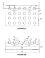
- a wafer 350 includes a plurality of light emitting devices 360 thereon.
- the wafer 350 may be a growth wafer on which the light emitting devices are grown and/or may be a carrier wafer on which the light emitting devices have been mounted.
- the light emitting devices 360 include a plurality of discrete phosphor-containing regions thereon, which are illustrated schematically by the layers 370 on the light emitting devices 360 . Regions 390 between the light emitting devices 360 , which may correspond to saw streets, may not include the discrete phosphor-containing regions 370 .
- the dicing saw 380 may not cut through the phosphor-containing regions 370 . Since the phosphor particles in the phosphor-containing regions 370 are abrasive, it may cause undue wear to the blade of the dicing saw 380 to cut through phosphor-containing regions such as the discrete phosphor-containing regions 370 .
- the wafer 350 may be diced to provide individual light emitting diodes 395 including discrete phosphor-containing regions 370 thereon.
- the substrate 350 may be removed from the light emitting devices 360 .
- a light emitting diode 495 including a light emitting device 360 that has been removed from a substrate is illustrated.
- a light scattering layer 710 as described above may be formed on the discrete phosphor-containing regions 370 , such that the discrete phosphor-containing regions 370 are between the light scattering layer 710 and the light emitting device 360 .
- the discrete phosphor-containing regions 370 may be formed on a light scattering layer 710 , such that the light scattering layer 710 is between the discrete phosphor-containing regions 370 and the light emitting device 360 .
- an LED structure 100 is prepared, for example, by forming an active region and one or more window layers thereon (Block 910 ).
- the LED structure 100 may also be mounted and cleaned in preparation for forming discrete phosphor-containing regions thereon.
- a phosphor loaded photosensitive layer 410 such as a photopatternable silicone, is spin-coated onto the LED structure 100 (Block 920 ), and the photosensitive layer 410 is at least partially cured, for example, to stabilize the layer (Block 930 ).
- the phosphor-loaded photosensitive layer 410 includes therein phosphor particles configured to convert light emitted by the active region in the LED structure 100 to a different wavelength.
- a mask 420 is applied to the stabilized phosphor loaded photosensitive layer 410 (Block 940 ).
- the mask 420 is patterned to expose portions of the LED structure 100 on which discrete phosphor-containing regions are to be formed.
- the LED structure 100 including the phosphor loaded photosensitive layer 410 is exposed with light having a wavelength sufficient to cure the phosphor loaded photosensitive layer 410 (Block 950 ).
- the mask 420 and the unexposed portions of the phosphor loaded photosensitive layer 410 are then removed (Block 960 ) to provide discrete phosphor-containing regions 430 .
- the LED structure 100 is then diced to provide individual semiconductor light emitting devices including discrete phosphor-containing regions 430 (Block 970 ).
- a micro-screen 190 can be applied to an LED structure 100 to at wafer level (or die level).
- the micro-screen 190 can include a material such as a fine filament woven fabric or other material used for filtering particulate materials. Micro-screen filters are well known in the material filtering art.
- the micro-screen 190 includes openings 192 therein that expose the LED structure 100 and that have a width selected to permit a desired size of phosphor particle 130 A to contact the LED structure therethrough.
- the phosphor particles 130 A may be deposited, and then the screen may be removed, leaving the phosphor particles on the LED structure in a desired pattern.
- Additional particles 130 B may then be deposited, and may organize in the spaces previously occupied by the screen, as shown in FIG. 14B .
- the additional phosphor particles 130 B may have at least one optical property different from the phosphor particles 130 A.
- the additional phosphor particles 130 B may convert incident light to a different color than the phosphor particles 130 A, and/or the additional phosphor particles 130 B may scatter incident light in a different pattern than the phosphor particles 130 A.
- an overlayer 140 may be formed on the LED structure 100 including the organized phosphor particles 130 A, 130 B.
- the overlayer 140 may include, for example, a layer of silicone or other encapsulant material, and in some embodiments may include a phosphor-loaded material. In some embodiments, the overlayer 140 may include a different phosphor material from the phosphor material contained in the organized phosphor particles 130 A, 130 B.
- the overlayer 140 may include other materials/structures that can change optical properties of light emitted by the LED structure 100 .
- the overlayer 140 can include optical diffusing/scattering particles and/or the overlayer 140 can be textured and/or patterned to increase optical extraction from the device.
- Some silicones can be formulated to be very tacky after curing. Such materials are typically referred to as soft gels. This property can be used to advantage by adhering a tacky silicone on a surface and embedding phosphor from a micro-screen loaded with phosphor into the silicone. In other embodiments, a harder silicone with low tack may be used so that phosphor particles can move across a surface as depicted, for example, in FIG. 5 .
- a transparent layer can be formed by pressing into it in a partial cure state for example, then finishing cure, to form particle organizing layer.
- a transparent silicone layer 194 may be formed on an LED structure 100 .
- the silicone layer 194 may or may not include embedded phosphors 130 A.
- Portions of the transparent layer 194 of, for example, a matrix material such as silicone, may be selectively cured.
- a heated plate 196 with ridges 198 may be brought into proximity with the silicone layer 194 , causing selected portions 194 A of the transparent layer 194 adjacent the heated ridges to cure.
- the remaining uncured portions of the transparent layer 194 are removed, leaving a cured phosphor-organizing layer including cured portions 194 A. Additional phosphor particles 130 may be deposited in the space previously occupied by the uncured portions of the transparent layer 194 .
- an overlayer 140 may be formed on the LED structure 100 including the phosphor particles 130 and cured portions 194 A.
- the overlayer 140 may include, for example, a layer of silicone or other encapsulant material, and in some embodiments may include a phosphor-loaded material. In some embodiments, the overlayer 140 may include a different phosphor material from the phosphor material contained in the phosphor particles 130 .
- the overlayer 140 may include other materials/structures that can change optical properties of light emitted by the LED structure 100 .
- the overlayer 140 can include optical diffusing/scattering particles and/or the overlayer 140 can be textured and/or patterned to increase optical extraction from the device.
- different sized phosphors can be used to promote phosphor organization.
- a larger transparent particle 132 such as a glass bead or ball (which are commercially available in various RI grades) may be deposited first. Then gaps between the larger particles 132 may be filled with smaller phosphor particles 130 .
- an overlayer 140 may be formed on the LED structure 100 including the phosphor particles 130 and transparent particles 132 .
- the overlayer 140 may include, for example, a layer of silicone or other encapsulant material, and in some embodiments may include a phosphor-loaded material. In some embodiments, the overlayer 140 may include a different phosphor material from the phosphor material contained in the phosphor particles 130 .
- the overlayer 140 may include other materials/structures that can change optical properties of light emitted by the LED structure 100 .
- the overlayer 140 can include optical diffusing/scattering particles and/or the overlayer 140 can be textured and/or patterned to increase optical extraction from the device.
Landscapes
- Led Device Packages (AREA)
- Led Devices (AREA)
Abstract
Description
Claims (17)
Priority Applications (1)
| Application Number | Priority Date | Filing Date | Title |
|---|---|---|---|
| US12/976,769 US9054282B2 (en) | 2007-08-07 | 2010-12-22 | Semiconductor light emitting devices with applied wavelength conversion materials and methods for forming the same |
Applications Claiming Priority (2)
| Application Number | Priority Date | Filing Date | Title |
|---|---|---|---|
| US11/835,044 US7863635B2 (en) | 2007-08-07 | 2007-08-07 | Semiconductor light emitting devices with applied wavelength conversion materials |
| US12/976,769 US9054282B2 (en) | 2007-08-07 | 2010-12-22 | Semiconductor light emitting devices with applied wavelength conversion materials and methods for forming the same |
Related Parent Applications (1)
| Application Number | Title | Priority Date | Filing Date |
|---|---|---|---|
| US11/835,044 Continuation US7863635B2 (en) | 2007-08-07 | 2007-08-07 | Semiconductor light emitting devices with applied wavelength conversion materials |
Publications (2)
| Publication Number | Publication Date |
|---|---|
| US20110089456A1 US20110089456A1 (en) | 2011-04-21 |
| US9054282B2 true US9054282B2 (en) | 2015-06-09 |
Family
ID=39869682
Family Applications (2)
| Application Number | Title | Priority Date | Filing Date |
|---|---|---|---|
| US11/835,044 Active 2028-03-14 US7863635B2 (en) | 2007-08-07 | 2007-08-07 | Semiconductor light emitting devices with applied wavelength conversion materials |
| US12/976,769 Active 2028-06-13 US9054282B2 (en) | 2007-08-07 | 2010-12-22 | Semiconductor light emitting devices with applied wavelength conversion materials and methods for forming the same |
Family Applications Before (1)
| Application Number | Title | Priority Date | Filing Date |
|---|---|---|---|
| US11/835,044 Active 2028-03-14 US7863635B2 (en) | 2007-08-07 | 2007-08-07 | Semiconductor light emitting devices with applied wavelength conversion materials |
Country Status (2)
| Country | Link |
|---|---|
| US (2) | US7863635B2 (en) |
| WO (1) | WO2009020547A2 (en) |
Families Citing this family (41)
| Publication number | Priority date | Publication date | Assignee | Title |
|---|---|---|---|---|
| WO2008044759A1 (en) * | 2006-10-12 | 2008-04-17 | Panasonic Corporation | Light-emitting device and method for manufacturing the same |
| US7781779B2 (en) * | 2007-05-08 | 2010-08-24 | Luminus Devices, Inc. | Light emitting devices including wavelength converting material |
| KR20090002835A (en) * | 2007-07-04 | 2009-01-09 | 엘지전자 주식회사 | Nitride-based light emitting device and its manufacturing method |
| JP4829190B2 (en) * | 2007-08-22 | 2011-12-07 | 株式会社東芝 | Light emitting element |
| US8946987B2 (en) * | 2007-11-07 | 2015-02-03 | Industrial Technology Research Institute | Light emitting device and fabricating method thereof |
| US20090309114A1 (en) * | 2008-01-16 | 2009-12-17 | Luminus Devices, Inc. | Wavelength converting light-emitting devices and methods of making the same |
| KR100973238B1 (en) * | 2008-03-26 | 2010-07-30 | 서울반도체 주식회사 | LED comprising phosphor coating method and apparatus and phosphor coating layer |
| US7868340B2 (en) * | 2008-05-30 | 2011-01-11 | Bridgelux, Inc. | Method and apparatus for generating white light from solid state light emitting devices |
| US8742441B2 (en) * | 2008-09-10 | 2014-06-03 | Tsmc Solid State Lighting Ltd. | Light-emitting diode with embedded elements |
| US20100117106A1 (en) * | 2008-11-07 | 2010-05-13 | Ledengin, Inc. | Led with light-conversion layer |
| US8933526B2 (en) * | 2009-07-15 | 2015-01-13 | First Solar, Inc. | Nanostructured functional coatings and devices |
| KR101020998B1 (en) * | 2009-11-12 | 2011-03-09 | 엘지이노텍 주식회사 | Light emitting device and manufacturing method |
| KR101857772B1 (en) | 2010-03-16 | 2018-06-28 | 필립스 라이팅 홀딩 비.브이. | Lighting apparatus |
| DE102010022561A1 (en) * | 2010-06-02 | 2011-12-08 | Osram Opto Semiconductors Gmbh | Wavelength conversion element, optoelectronic component with a wavelength conversion element and method for producing a wavelength conversion element |
| KR101726807B1 (en) * | 2010-11-01 | 2017-04-14 | 삼성전자주식회사 | Light Emitting Device |
| DE102010051286A1 (en) * | 2010-11-12 | 2012-05-16 | Osram Opto Semiconductors Gmbh | Optoelectronic semiconductor chip and method for its production |
| TW201222878A (en) * | 2010-11-23 | 2012-06-01 | Siliconware Precision Industries Co Ltd | Light-permeating cover board, fabrication method thereof, and package structure having LED |
| WO2012091008A1 (en) * | 2010-12-28 | 2012-07-05 | 日亜化学工業株式会社 | Semiconductor light-emitting device |
| CN102563543B (en) | 2011-05-09 | 2015-01-07 | 深圳市绎立锐光科技开发有限公司 | Method and light source for generating high-brightness homogeneous light based on optical wavelength conversion |
| DE102011079782A1 (en) * | 2011-07-26 | 2013-01-31 | Osram Ag | Semiconductor emitter and method for generating useful light from laser light |
| DE102011111980A1 (en) | 2011-08-29 | 2013-02-28 | Osram Opto Semiconductors Gmbh | Method for producing a light-emitting diode and light-emitting diode |
| US8492746B2 (en) * | 2011-09-12 | 2013-07-23 | SemiLEDs Optoelectronics Co., Ltd. | Light emitting diode (LED) dice having wavelength conversion layers |
| US10310363B2 (en) | 2011-09-22 | 2019-06-04 | Delta Electronics, Inc. | Phosphor device with spectrum of converted light comprising at least a color light |
| TWI448806B (en) | 2011-09-22 | 2014-08-11 | Delta Electronics Inc | Phosphor device and illumination system and projection equipment with the same |
| US10688527B2 (en) | 2011-09-22 | 2020-06-23 | Delta Electronics, Inc. | Phosphor device comprising plural phosphor agents for converting waveband light into plural color lights with different wavelength peaks |
| JP5902908B2 (en) | 2011-10-19 | 2016-04-13 | スタンレー電気株式会社 | Semiconductor light emitting device and vehicle lamp |
| US8884508B2 (en) | 2011-11-09 | 2014-11-11 | Cree, Inc. | Solid state lighting device including multiple wavelength conversion materials |
| DE102012202927B4 (en) * | 2012-02-27 | 2021-06-10 | Osram Gmbh | LIGHT SOURCE WITH LED CHIP AND LUMINOUS LAYER |
| TW201347231A (en) * | 2012-05-04 | 2013-11-16 | Lextar Electronics Corp | Light-emitting diode component |
| DE102012212086A1 (en) * | 2012-07-11 | 2014-01-16 | Osram Opto Semiconductors Gmbh | METHOD FOR PRODUCING A COMPONENT OF AN OPTOELECTRONIC COMPONENT AND METHOD FOR MANUFACTURING AN OPTOELECTRONIC COMPONENT |
| US8772814B2 (en) * | 2012-10-26 | 2014-07-08 | Nthdegree Technologies Worldwide Inc. | Phosphor layer containing transparent particles over blue LED |
| KR20140076767A (en) * | 2012-12-13 | 2014-06-23 | (주)라이타이저코리아 | Fabricating for Fluorescent Substance of Light Emitting Diode |
| CN105531833B (en) * | 2013-05-15 | 2018-01-30 | 皇家飞利浦有限公司 | LED with scattering features in substrate |
| CN104425661B (en) * | 2013-08-22 | 2017-03-01 | 展晶科技(深圳)有限公司 | Light-emitting diode and its manufacturing method |
| EP3117267B1 (en) * | 2014-03-11 | 2018-05-02 | Osram Sylvania Inc. | Light converter assemblies with enhanced heat dissipation |
| KR102203690B1 (en) * | 2014-08-21 | 2021-01-15 | 엘지이노텍 주식회사 | Phosphor plate and manufacturing method thereof |
| DE102016122251A1 (en) * | 2016-11-18 | 2018-05-24 | Infineon Technologies Austria Ag | Method of forming semiconductor devices and semiconductor device |
| WO2018183341A1 (en) | 2017-03-27 | 2018-10-04 | Firouzeh Sabri | Light weight flexible temperature sensor kit |
| DE102018125632A1 (en) * | 2018-10-16 | 2020-04-16 | Osram Opto Semiconductors Gmbh | OPTOELECTRONIC COMPONENT WITH A MARKING AND METHOD FOR PRODUCING OPTOELECTRONIC COMPONENTS |
| CN115602780A (en) * | 2021-07-08 | 2023-01-13 | 抱朴科技股份有限公司(Tw) | Method for manufacturing flip chip type light emitting diode device with high light extraction rate and product thereof |
| US20230265337A1 (en) * | 2022-02-22 | 2023-08-24 | Ams-Osram International Gmbh | Converter element, method for producing a converter element and radiation emitting device |
Citations (295)
| Publication number | Priority date | Publication date | Assignee | Title |
|---|---|---|---|---|
| US3805937A (en) | 1970-12-29 | 1974-04-23 | Glory Kogyo Kk | Automatic money dispensing machine |
| US3875456A (en) | 1972-04-04 | 1975-04-01 | Hitachi Ltd | Multi-color semiconductor lamp |
| US3927290A (en) | 1974-11-14 | 1975-12-16 | Teletype Corp | Selectively illuminated pushbutton switch |
| US4120026A (en) | 1975-08-21 | 1978-10-10 | Mitsubishi Denki Kabushiki Kaisha | Method of mixed illumination |
| US4325146A (en) | 1979-12-20 | 1982-04-13 | Lennington John W | Non-synchronous object identification system |
| US4408157A (en) | 1981-05-04 | 1983-10-04 | Associated Research, Inc. | Resistance measuring arrangement |
| US4420398A (en) | 1981-08-13 | 1983-12-13 | American National Red Cross | Filteration method for cell produced antiviral substances |
| US4710699A (en) | 1983-10-14 | 1987-12-01 | Omron Tateisi Electronics Co. | Electronic switching device |
| US4772885A (en) | 1984-11-22 | 1988-09-20 | Ricoh Company, Ltd. | Liquid crystal color display device |
| US4918497A (en) | 1988-12-14 | 1990-04-17 | Cree Research, Inc. | Blue light emitting diode formed in silicon carbide |
| US4966862A (en) | 1989-08-28 | 1990-10-30 | Cree Research, Inc. | Method of production of light emitting diodes |
| DE3916875A1 (en) | 1989-05-24 | 1990-12-06 | Ullmann Ulo Werk | Signal light esp. multi-compartment signal lights for motor vehicle - uses green, red, and blue LED's combined so that single light is given with help of mix optics |
| US5027168A (en) | 1988-12-14 | 1991-06-25 | Cree Research, Inc. | Blue light emitting diode formed in silicon carbide |
| US5087883A (en) | 1990-09-10 | 1992-02-11 | Mr. Coffee, Inc. | Differential conductivity meter for fluids and products containing such meters |
| JPH04159519A (en) | 1990-10-24 | 1992-06-02 | Stanley Electric Co Ltd | Liquid crystal display device with led backlight and its manufacture |
| US5166815A (en) | 1991-02-28 | 1992-11-24 | Novatel Communications, Ltd. | Liquid crystal display and reflective diffuser therefor including a reflection cavity section and an illumination cavity section |
| US5210051A (en) | 1990-03-27 | 1993-05-11 | Cree Research, Inc. | High efficiency light emitting diodes from bipolar gallium nitride |
| US5264997A (en) | 1992-03-04 | 1993-11-23 | Dominion Automotive Industries Corp. | Sealed, inductively powered lamp assembly |
| US5338944A (en) | 1993-09-22 | 1994-08-16 | Cree Research, Inc. | Blue light-emitting diode with degenerate junction structure |
| US5393993A (en) | 1993-12-13 | 1995-02-28 | Cree Research, Inc. | Buffer structure between silicon carbide and gallium nitride and resulting semiconductor devices |
| US5407799A (en) | 1989-09-14 | 1995-04-18 | Associated Universities, Inc. | Method for high-volume sequencing of nucleic acids: random and directed priming with libraries of oligonucleotides |
| US5410519A (en) | 1993-11-19 | 1995-04-25 | Coastal & Offshore Pacific Corporation | Acoustic tracking system |
| US5416342A (en) | 1993-06-23 | 1995-05-16 | Cree Research, Inc. | Blue light-emitting diode with high external quantum efficiency |
| US5477436A (en) | 1992-08-29 | 1995-12-19 | Robert Bosch Gmbh | Illuminating device for motor vehicles |
| US5523589A (en) | 1994-09-20 | 1996-06-04 | Cree Research, Inc. | Vertical geometry light emitting diode with group III nitride active layer and extended lifetime |
| US5604135A (en) | 1994-08-12 | 1997-02-18 | Cree Research, Inc. | Method of forming green light emitting diode in silicon carbide |
| US5631190A (en) | 1994-10-07 | 1997-05-20 | Cree Research, Inc. | Method for producing high efficiency light-emitting diodes and resulting diode structures |
| JPH09146089A (en) | 1995-11-28 | 1997-06-06 | Masahiko Yamamoto | Surface light source for color display device and liquid crystal display device |
| US5739554A (en) | 1995-05-08 | 1998-04-14 | Cree Research, Inc. | Double heterojunction light emitting diode with gallium nitride active layer |
| JPH10163535A (en) | 1996-11-27 | 1998-06-19 | Kasei Optonix Co Ltd | White light emitting element |
| US5779924A (en) | 1996-03-22 | 1998-07-14 | Hewlett-Packard Company | Ordered interface texturing for a light emitting device |
| US5803579A (en) | 1996-06-13 | 1998-09-08 | Gentex Corporation | Illuminator assembly incorporating light emitting diodes |
| WO1998043014A1 (en) | 1997-03-26 | 1998-10-01 | Dana Bruce | Low power lighting display |
| US5851063A (en) | 1996-10-28 | 1998-12-22 | General Electric Company | Light-emitting diode white light source |
| US5959316A (en) | 1998-09-01 | 1999-09-28 | Hewlett-Packard Company | Multiple encapsulation of phosphor-LED devices |
| WO1999066483A1 (en) | 1998-06-19 | 1999-12-23 | Cambridge Display Technology Ltd. | Backlit displays |
| EP0971421A2 (en) | 1998-07-09 | 2000-01-12 | Sumitomo Electric Industries, Ltd. | White color light emitting diode and neutral color light emitting diode |
| JP2000022222A (en) | 1998-07-07 | 2000-01-21 | Stanley Electric Co Ltd | Light emitting diode |
| US6043509A (en) | 1996-12-13 | 2000-03-28 | Hitachi Cable, Ltd. | Light-emitting diode having moisture-proof characteristics and high output power |
| US6066861A (en) | 1996-09-20 | 2000-05-23 | Siemens Aktiengesellschaft | Wavelength-converting casting composition and its use |
| US6071795A (en) | 1998-01-23 | 2000-06-06 | The Regents Of The University Of California | Separation of thin films from transparent substrates by selective optical processing |
| WO2000034709A1 (en) | 1998-12-09 | 2000-06-15 | Rensselaer Polytechnic Institute | Led lamp with reflector and multicolor adjuster |
| US6076936A (en) | 1996-11-25 | 2000-06-20 | George; Ben | Tread area and step edge lighting system |
| JP2000183408A (en) | 1998-12-16 | 2000-06-30 | Toshiba Electronic Engineering Corp | Semiconductor light emitting device |
| US6084250A (en) | 1997-03-03 | 2000-07-04 | U.S. Philips Corporation | White light emitting diode |
| US6095666A (en) | 1997-09-12 | 2000-08-01 | Unisplay S.A. | Light source |
| US6144429A (en) * | 1996-01-25 | 2000-11-07 | Kabushiki Kaisha Toshiba | Liquid-crystal display device |
| US6187606B1 (en) | 1997-10-07 | 2001-02-13 | Cree, Inc. | Group III nitride photonic devices on silicon carbide substrates with conductive buffer interlayer structure |
| US6212213B1 (en) | 1999-01-29 | 2001-04-03 | Agilent Technologies, Inc. | Projector light source utilizing a solid state green light source |
| JP2001111114A (en) | 1999-10-06 | 2001-04-20 | Sony Corp | White LED |
| US6234648B1 (en) | 1998-09-28 | 2001-05-22 | U.S. Philips Corporation | Lighting system |
| US20010002049A1 (en) | 1996-06-26 | 2001-05-31 | Osram Opto Semiconductors Gmbh & Co., Ohg | Light-radiating semiconductor component with a luminescence conversion element |
| WO2001041215A1 (en) | 1999-12-02 | 2001-06-07 | Koninklijke Philips Electronics N.V. | Hybrid white light source comprising led and phosphor-led |
| JP2001156331A (en) | 1999-11-30 | 2001-06-08 | Nichia Chem Ind Ltd | Nitride semiconductor light emitting device |
| WO2001043113A1 (en) | 1999-12-09 | 2001-06-14 | Koninklijke Philips Electronics N.V. | Display systems incorporating light-emitting diode light source |
| US6252254B1 (en) | 1998-02-06 | 2001-06-26 | General Electric Company | Light emitting device with phosphor composition |
| US6255670B1 (en) | 1998-02-06 | 2001-07-03 | General Electric Company | Phosphors for light generation from light emitting semiconductors |
| US6278135B1 (en) | 1998-02-06 | 2001-08-21 | General Electric Company | Green-light emitting phosphors and light sources using the same |
| US6292901B1 (en) | 1997-08-26 | 2001-09-18 | Color Kinetics Incorporated | Power/data protocol |
| WO2001069692A1 (en) | 2000-03-14 | 2001-09-20 | Lumileds Lighting B.V. | Light-emitting diode, lighting device and method of manufacturing same |
| US6294800B1 (en) | 1998-02-06 | 2001-09-25 | General Electric Company | Phosphors for white light generation from UV emitting diodes |
| JP2001307506A (en) | 2000-04-17 | 2001-11-02 | Hitachi Ltd | White light emitting device and lighting equipment |
| US6319425B1 (en) | 1997-07-07 | 2001-11-20 | Asahi Rubber Inc. | Transparent coating member for light-emitting diodes and a fluorescent color light source |
| EP1160883A2 (en) | 2000-05-31 | 2001-12-05 | Matsushita Electric Industrial Co., Ltd. | LED lamp |
| US6329676B1 (en) | 1999-03-01 | 2001-12-11 | Toru Takayama | Flat panel solid state light source |
| US6335538B1 (en) | 1999-07-23 | 2002-01-01 | Impulse Dynamics N.V. | Electro-optically driven solid state relay system |
| US20020006044A1 (en) | 2000-05-04 | 2002-01-17 | Koninklijke Philips Electronics N.V. | Assembly of a display device and an illumination system |
| US20020015013A1 (en) | 2000-06-28 | 2002-02-07 | Larry Ragle | Integrated color LED chip |
| US6348766B1 (en) | 1999-11-05 | 2002-02-19 | Avix Inc. | Led Lamp |
| US6350041B1 (en) | 1999-12-03 | 2002-02-26 | Cree Lighting Company | High output radial dispersing lamp using a solid state light source |
| US6357889B1 (en) | 1999-12-01 | 2002-03-19 | General Electric Company | Color tunable light source |
| EP1193772A2 (en) | 2000-09-29 | 2002-04-03 | Citizen Electronics Co., Ltd. | Light emitting diode with wavelength conversion and absorbing material |
| US6373188B1 (en) | 1998-12-22 | 2002-04-16 | Honeywell International Inc. | Efficient solid-state light emitting device with excited phosphors for producing a visible light output |
| JP2002150821A (en) | 2000-11-06 | 2002-05-24 | Citizen Electronics Co Ltd | Surface light source |
| US6394621B1 (en) | 2000-03-30 | 2002-05-28 | Hanewinkel, Iii William Henry | Latching switch for compact flashlight providing an easy means for changing the power source |
| US20020068201A1 (en) | 1994-01-27 | 2002-06-06 | Vaudo Robert P. | Free-standing (Al, Ga, In)N and parting method for forming same |
| US20020087532A1 (en) | 2000-12-29 | 2002-07-04 | Steven Barritz | Cooperative, interactive, heuristic system for the creation and ongoing modification of categorization systems |
| US6420199B1 (en) | 1999-02-05 | 2002-07-16 | Lumileds Lighting, U.S., Llc | Methods for fabricating light emitting devices having aluminum gallium indium nitride structures and mirror stacks |
| US6429583B1 (en) | 1998-11-30 | 2002-08-06 | General Electric Company | Light emitting device with ba2mgsi2o7:eu2+, ba2sio4:eu2+, or (srxcay ba1-x-y)(a1zga1-z)2sr:eu2+phosphors |
| US6441558B1 (en) | 2000-12-07 | 2002-08-27 | Koninklijke Philips Electronics N.V. | White LED luminary light control system |
| US20020123164A1 (en) | 2001-02-01 | 2002-09-05 | Slater David B. | Light emitting diodes including modifications for light extraction and manufacturing methods therefor |
| US20020139987A1 (en) | 2001-03-29 | 2002-10-03 | Collins William David | Monolithic series/parallel led arrays formed on highly resistive substrates |
| US20020149576A1 (en) | 2001-03-30 | 2002-10-17 | Yukio Tanaka | Display |
| US6480299B1 (en) | 1997-11-25 | 2002-11-12 | University Technology Corporation | Color printer characterization using optimization theory and neural networks |
| US6501100B1 (en) | 2000-05-15 | 2002-12-31 | General Electric Company | White light emitting phosphor blend for LED devices |
| US6504179B1 (en) | 2000-05-29 | 2003-01-07 | Patent-Treuhand-Gesellschaft Fur Elektrische Gluhlampen Mbh | Led-based white-emitting illumination unit |
| US6504180B1 (en) | 1998-07-28 | 2003-01-07 | Imec Vzw And Vrije Universiteit | Method of manufacturing surface textured high-efficiency radiating devices and devices obtained therefrom |
| US20030006418A1 (en) | 2001-05-30 | 2003-01-09 | Emerson David Todd | Group III nitride based light emitting diode structures with a quantum well and superlattice, group III nitride based quantum well structures and group III nitride based superlattice structures |
| US20030026096A1 (en) | 2001-07-31 | 2003-02-06 | Patent-Treuhand-Gesellschaft Fur Elektrische Gluhlampen Mbh | LED-based planar light source |
| US20030030063A1 (en) | 2001-07-27 | 2003-02-13 | Krzysztof Sosniak | Mixed color leds for auto vanity mirrors and other applications where color differentiation is critical |
| US6522065B1 (en) | 2000-03-27 | 2003-02-18 | General Electric Company | Single phosphor for creating white light with high luminosity and high CRI in a UV led device |
| US20030042908A1 (en) | 1999-11-19 | 2003-03-06 | Gelcore Llc | Method and device for remote monitoring of LED lamps |
| US6538371B1 (en) | 2000-03-27 | 2003-03-25 | The General Electric Company | White light illumination system with improved color output |
| US6552495B1 (en) | 2001-12-19 | 2003-04-22 | Koninklijke Philips Electronics N.V. | Adaptive control system and method with spatial uniform color metric for RGB LED based white light illumination |
| US6550949B1 (en) | 1996-06-13 | 2003-04-22 | Gentex Corporation | Systems and components for enhancing rear vision from a vehicle |
| US6559075B1 (en) | 1996-10-01 | 2003-05-06 | Siemens Aktiengesellschaft | Method of separating two layers of material from one another and electronic components produced using this process |
| US20030089918A1 (en) | 2001-10-31 | 2003-05-15 | Norbert Hiller | Broad spectrum light emitting devices and methods and systems for fabricating the same |
| US6578986B2 (en) | 2001-06-29 | 2003-06-17 | Permlight Products, Inc. | Modular mounting arrangement and method for light emitting diodes |
| WO2003056876A2 (en) | 2001-12-14 | 2003-07-10 | Digital Optics International Corporation | Uniform illumination system |
| US6592810B2 (en) | 2000-03-17 | 2003-07-15 | Hitachi Metals, Ltd. | Fe-ni alloy having high strength and low thermal expansion, a shadow mask made of the alloy, a braun tube with the shadow mask, a lead frame made of the alloy and a semiconductor element with lead frame |
| US6600175B1 (en) | 1996-03-26 | 2003-07-29 | Advanced Technology Materials, Inc. | Solid state white light emitter and display using same |
| US6603258B1 (en) | 2000-04-24 | 2003-08-05 | Lumileds Lighting, U.S. Llc | Light emitting diode device that emits white light |
| US20030146411A1 (en) | 2001-05-21 | 2003-08-07 | Srivastava Alok Mani | Yellow light-emitting halophosphate phosphors and light sources incorporating the same |
| TW546854B (en) | 2002-05-21 | 2003-08-11 | Harvatek Corp | White light emitting device |
| US6624350B2 (en) | 2001-01-18 | 2003-09-23 | Arise Technologies Corporation | Solar power management system |
| US6635503B2 (en) | 2002-01-28 | 2003-10-21 | Cree, Inc. | Cluster packaging of light emitting diodes |
| US6636003B2 (en) | 2000-09-06 | 2003-10-21 | Spectrum Kinetics | Apparatus and method for adjusting the color temperature of white semiconduct or light emitters |
| US6642666B1 (en) | 2000-10-20 | 2003-11-04 | Gelcore Company | Method and device to emulate a railway searchlight signal with light emitting diodes |
| WO2003091771A1 (en) | 2002-04-25 | 2003-11-06 | Koninklijke Philips Electronics N.V. | Compact lighting system and display device |
| US20030209997A1 (en) | 1999-11-19 | 2003-11-13 | Gelcore, Llc | Module for powering and monitoring light-emitting diodes |
| US6657236B1 (en) | 1999-12-03 | 2003-12-02 | Cree Lighting Company | Enhanced light extraction in LEDs through the use of internal and external optical elements |
| EP1367655A1 (en) | 2001-09-03 | 2003-12-03 | Matsushita Electric Industrial Co., Ltd. | SEMICONDUCTOR LIGHT EMITTING DEVICE, LIGHT EMITTING APPARATUS AND PRODUCTION METHOD FOR SEMICONDUCTOR LIGHT EMITTING DEVICE |
| US20030222268A1 (en) | 2002-05-31 | 2003-12-04 | Yocom Perry Niel | Light sources having a continuous broad emission wavelength and phosphor compositions useful therefor |
| EP1380876A1 (en) | 2002-07-11 | 2004-01-14 | Kabushiki Kaisha Toyota Jidoshokki | Reflecting colour liquid crystal display |
| US6685852B2 (en) | 2001-04-27 | 2004-02-03 | General Electric Company | Phosphor blends for generating white light from near-UV/blue light-emitting devices |
| US6686691B1 (en) | 1999-09-27 | 2004-02-03 | Lumileds Lighting, U.S., Llc | Tri-color, white light LED lamps |
| US6703173B2 (en) | 2001-11-23 | 2004-03-09 | Industrial Technology Research Institute | Color filters for liquid crystal display panels and method of producing the same |
| JP2004080046A (en) | 2000-05-31 | 2004-03-11 | Matsushita Electric Ind Co Ltd | LED lamps and lamp units |
| US20040046178A1 (en) | 2002-08-29 | 2004-03-11 | Citizen Electronics Co., Ltd. | Light emitting diode device |
| US20040051111A1 (en) | 2000-12-28 | 2004-03-18 | Koichi Ota | Light emitting device |
| US20040056260A1 (en) | 2002-09-19 | 2004-03-25 | Slater David B. | Phosphor-coated light emitting diodes including tapered sidewalls, and fabrication methods therefor |
| US6712486B1 (en) | 1999-10-19 | 2004-03-30 | Permlight Products, Inc. | Mounting arrangement for light emitting diodes |
| JP2004103443A (en) | 2002-09-11 | 2004-04-02 | Toshiba Lighting & Technology Corp | LED lighting device |
| US20040075399A1 (en) | 2002-10-22 | 2004-04-22 | Hall David Charles | LED light engine for AC operation and methods of fabricating same |
| US20040105264A1 (en) | 2002-07-12 | 2004-06-03 | Yechezkal Spero | Multiple Light-Source Illuminating System |
| WO2004068909A1 (en) | 2003-01-27 | 2004-08-12 | Matsushita Electric Industrial Co., Ltd. | Multichip led lighting device |
| US6784463B2 (en) | 1997-06-03 | 2004-08-31 | Lumileds Lighting U.S., Llc | III-Phospide and III-Arsenide flip chip light-emitting devices |
| JP2004253309A (en) | 2003-02-21 | 2004-09-09 | Nichia Chem Ind Ltd | Special-purpose LED lighting with color rendering properties |
| US6791257B1 (en) | 1999-02-05 | 2004-09-14 | Japan Energy Corporation | Photoelectric conversion functional element and production method thereof |
| US6800500B2 (en) | 1999-02-05 | 2004-10-05 | Lumileds Lighting U.S., Llc | III-nitride light emitting devices fabricated by substrate removal |
| US20040212998A1 (en) | 2003-04-25 | 2004-10-28 | Ferenc Mohacsi | Sign illumination system |
| US20040218387A1 (en) | 2003-03-18 | 2004-11-04 | Robert Gerlach | LED lighting arrays, fixtures and systems and method for determining human color perception |
| US20040218388A1 (en) | 2003-03-31 | 2004-11-04 | Fujitsu Display Technologies Corporation | Surface lighting device and liquid crystal display device using the same |
| US6817735B2 (en) | 2001-05-24 | 2004-11-16 | Matsushita Electric Industrial Co., Ltd. | Illumination light source |
| US20040239839A1 (en) | 2003-06-02 | 2004-12-02 | Hyung-Ki Hong | Liquid crystal display and method and apparatus for driving the same |
| JP2004356116A (en) | 2003-05-26 | 2004-12-16 | Citizen Electronics Co Ltd | Light emitting diode |
| JP2004363055A (en) | 2003-06-06 | 2004-12-24 | Stanley Electric Co Ltd | LED lighting device |
| US20040264212A1 (en) | 2003-06-30 | 2004-12-30 | Lg.Philips Lcd Co., Ltd. | Liquid crystal display module and driving apparatus thereof |
| US20040264193A1 (en) | 2001-08-23 | 2004-12-30 | Yukiyasu Okumura | Color temperature-regulable led light |
| JP2005005482A (en) | 2003-06-12 | 2005-01-06 | Citizen Electronics Co Ltd | LED light emitting device and color display device using the same |
| US6841804B1 (en) | 2003-10-27 | 2005-01-11 | Formosa Epitaxy Incorporation | Device of white light-emitting diode |
| WO2005004202A2 (en) | 2003-06-24 | 2005-01-13 | Gelcore Llc | Full spectrum phosphor blends for white light generation with led chips |
| US20050007306A1 (en) | 2003-05-29 | 2005-01-13 | Seiko Epson Corporation | Display device and projection display device |
| US20050006659A1 (en) | 2003-07-09 | 2005-01-13 | Ng Kee Yean | Light emitting diode utilizing a discrete wavelength-converting layer for color conversion |
| US6851834B2 (en) | 2001-12-21 | 2005-02-08 | Joseph A. Leysath | Light emitting diode lamp having parabolic reflector and diffuser |
| WO2005013365A2 (en) | 2003-07-30 | 2005-02-10 | Matsushita Electric Industrial Co., Ltd. | Semiconductor light emitting device, light emitting module, and lighting apparatus |
| DE10335077A1 (en) | 2003-07-31 | 2005-03-03 | Osram Opto Semiconductors Gmbh | LED module |
| WO2005022654A2 (en) | 2003-08-28 | 2005-03-10 | Matsushita Electric Industrial Co.,Ltd. | Semiconductor light emitting device, light emitting module, lighting apparatus, display element and manufacturing method of semiconductor light emitting device |
| US20050051790A1 (en) | 2003-06-05 | 2005-03-10 | Matsushita Electric Industrial Co., Ltd. | Phosphor, semiconductor light emitting device, and fabrication method thereof |
| JP2005101296A (en) | 2003-09-25 | 2005-04-14 | Osram-Melco Ltd | Variable color light emitting diode element, variable color light emitting diode module, and variable color light emitting diode lighting fixture |
| US6880954B2 (en) | 2002-11-08 | 2005-04-19 | Smd Software, Inc. | High intensity photocuring system |
| US6885035B2 (en) | 1999-12-22 | 2005-04-26 | Lumileds Lighting U.S., Llc | Multi-chip semiconductor LED assembly |
| JP2005142311A (en) | 2003-11-06 | 2005-06-02 | Tzu-Chi Cheng | Light emitting device |
| US20050116635A1 (en) | 2003-12-02 | 2005-06-02 | Walson James E. | Multiple LED source and method for assembling same |
| US20050133808A1 (en) | 2003-09-11 | 2005-06-23 | Kyocera Corporation | Package for housing light-emitting element, light-emitting apparatus and illumination apparatus |
| US6914267B2 (en) | 1999-06-23 | 2005-07-05 | Citizen Electronics Co. Ltd. | Light emitting diode |
| US20050151138A1 (en) | 2003-11-12 | 2005-07-14 | Slater David B.Jr. | Methods of processing semiconductor wafer backsides having light emitting devices (LEDS) thereon and leds so formed |
| EP1566848A2 (en) | 2004-02-23 | 2005-08-24 | LumiLeds Lighting U.S., LLC | Wavelength converted semiconductor light emitting device |
| US6936857B2 (en) | 2003-02-18 | 2005-08-30 | Gelcore, Llc | White light LED device |
| US20050190141A1 (en) | 2002-01-07 | 2005-09-01 | Shmuel Roth | Device and method for projection device based soft proofing |
| EP1571715A1 (en) | 2004-03-04 | 2005-09-07 | Nan Ya Plastics Corporation | Method for producing white light emission by means of secondary light exitation and its product |
| US20050215000A1 (en) | 2004-03-26 | 2005-09-29 | Negley Gerald H | Etching of substrates of light emitting devices |
| US20050227379A1 (en) | 2004-04-01 | 2005-10-13 | Matthew Donofrio | Laser patterning of light emitting devices and patterned light emitting devices |
| US20050231976A1 (en) | 2001-12-07 | 2005-10-20 | Keuper Matthijs H | Compact lighting system and display device |
| US6957899B2 (en) | 2002-10-24 | 2005-10-25 | Hongxing Jiang | Light emitting diodes for high AC voltage operation and general lighting |
| US20050243556A1 (en) | 2004-04-30 | 2005-11-03 | Manuel Lynch | Lighting system and method |
| WO2005104247A1 (en) | 2004-04-19 | 2005-11-03 | Matsushita Electric Industrial Co., Ltd. | Method for fabricating led illumination light source and led illumination light source |
| US20050251698A1 (en) | 2004-05-10 | 2005-11-10 | Manuel Lynch | Cuttable illuminated panel |
| US20050253151A1 (en) | 2002-08-29 | 2005-11-17 | Shiro Sakai | Light-emitting device having light-emitting elements |
| US6967116B2 (en) | 2003-02-14 | 2005-11-22 | Cree, Inc. | Light emitting device incorporating a luminescent material |
| US20050259423A1 (en) | 2004-05-24 | 2005-11-24 | Karsten Heuser | Light-emitting electronic component |
| US20050274972A1 (en) | 2004-06-10 | 2005-12-15 | Seoul Semiconductor Co., Ltd. | Light emitting device |
| US6980176B2 (en) | 2001-09-13 | 2005-12-27 | Hitdesign Ltd. | Three-dimensional image display apparatus and color reproducing method for three-dimensional image display |
| WO2005124877A2 (en) | 2004-06-18 | 2005-12-29 | Philips Intellectual Property & Standards Gmbh | Led with improve light emittance profile |
| US20060012989A1 (en) | 2004-07-16 | 2006-01-19 | Chi Lin Technology Co., Ltd. | Light emitting diode and backlight module having light emitting diode |
| US20060022582A1 (en) | 2004-08-02 | 2006-02-02 | Gelcore, Llc | White LEDs with tunable CRI |
| US7005679B2 (en) | 2003-05-01 | 2006-02-28 | Cree, Inc. | Multiple component solid state white light |
| US7009343B2 (en) | 2004-03-11 | 2006-03-07 | Kevin Len Li Lim | System and method for producing white light using LEDs |
| WO2006028312A1 (en) | 2004-09-10 | 2006-03-16 | Luxpia Co., Ltd. | Semiconductor device for emitting light and method for fabricating the same |
| US7014336B1 (en) | 1999-11-18 | 2006-03-21 | Color Kinetics Incorporated | Systems and methods for generating and modulating illumination conditions |
| US20060063289A1 (en) | 2004-09-21 | 2006-03-23 | Negley Gerald H | Methods of coating semiconductor light emitting elements by evaporating solvent from a suspension |
| US20060061259A1 (en) | 2004-09-23 | 2006-03-23 | Negley Gerald H | Semiconductor light emitting devices including patternable films comprising transparent silicone and phosphor, and methods of manufacturing same |
| US20060060872A1 (en) | 2004-09-22 | 2006-03-23 | Edmond John A | High output group III nitride light emitting diodes |
| US20060067073A1 (en) | 2004-09-30 | 2006-03-30 | Chu-Chi Ting | White led device |
| CN1767216A (en) | 2004-10-29 | 2006-05-03 | 三菱重工业株式会社 | photoelectric conversion device |
| US20060105482A1 (en) | 2004-11-12 | 2006-05-18 | Lumileds Lighting U.S., Llc | Array of light emitting devices to produce a white light source |
| US20060105485A1 (en) * | 2004-11-15 | 2006-05-18 | Lumileds Lighting U.S., Llc | Overmolded lens over LED die |
| US20060113548A1 (en) | 2004-11-29 | 2006-06-01 | Ching-Chung Chen | Light emitting diode |
| US7061454B2 (en) | 2002-07-18 | 2006-06-13 | Citizen Electronics Co., Ltd. | Light emitting diode device |
| WO2006061728A2 (en) | 2004-12-06 | 2006-06-15 | Koninklijke Philips Electronics N.V. | Single chip led as compact color variable light source |
| US20060124953A1 (en) | 2004-12-14 | 2006-06-15 | Negley Gerald H | Semiconductor light emitting device mounting substrates and packages including cavities and cover plates, and methods of packaging same |
| US7066623B2 (en) | 2003-12-19 | 2006-06-27 | Soo Ghee Lee | Method and apparatus for producing untainted white light using off-white light emitting diodes |
| US20060138937A1 (en) | 2004-12-28 | 2006-06-29 | James Ibbetson | High efficacy white LED |
| US20060152140A1 (en) | 2005-01-10 | 2006-07-13 | Brandes George R | Light emission device |
| US20060152172A9 (en) | 1997-12-17 | 2006-07-13 | Color Kinetics, Inc. | Methods and apparatus for generating and modulating white light illumination conditions |
| US7083302B2 (en) | 2004-03-24 | 2006-08-01 | J. S. Technology Co., Ltd. | White light LED assembly |
| US20060181192A1 (en) | 2004-08-02 | 2006-08-17 | Gelcore | White LEDs with tailorable color temperature |
| US7093958B2 (en) | 2002-04-09 | 2006-08-22 | Osram Sylvania Inc. | LED light source assembly |
| US7095056B2 (en) | 2003-12-10 | 2006-08-22 | Sensor Electronic Technology, Inc. | White light emitting device and method |
| US7102172B2 (en) | 2003-10-09 | 2006-09-05 | Permlight Products, Inc. | LED luminaire |
| US20060202105A1 (en) | 2005-03-14 | 2006-09-14 | Lumileds Lighting U.S., Llc | Wavelength-converted semiconductor light emitting device |
| US7118262B2 (en) | 2004-07-23 | 2006-10-10 | Cree, Inc. | Reflective optical elements for semiconductor light emitting devices |
| US20060226759A1 (en) * | 2005-03-06 | 2006-10-12 | Sharp Kabushiki Kaisha | Light emitting device and fabricating method thereof |
| WO2006111906A2 (en) | 2005-04-19 | 2006-10-26 | Philips Intellectual Property & Standards Gmbh | Illumination system comprising a red-emitting ceramic luminescence converter |
| US20060245184A1 (en) | 2005-04-29 | 2006-11-02 | Galli Robert D | Iris diffuser for adjusting light beam properties |
| US7135664B2 (en) | 2004-09-08 | 2006-11-14 | Emteq Lighting and Cabin Systems, Inc. | Method of adjusting multiple light sources to compensate for variation in light output that occurs with time |
| WO2006121196A1 (en) | 2005-05-12 | 2006-11-16 | Matsushita Electric Industrial Co., Ltd. | Led with a phosphor layer having different thikness or different phosphor concentration |
| US20070001994A1 (en) | 2001-06-11 | 2007-01-04 | Shmuel Roth | Multi-primary display with spectrally adapted back-illumination |
| US7164231B2 (en) | 2003-11-24 | 2007-01-16 | Samsung Sdi Co., Ltd. | Plasma display panel with defined phosphor layer thicknesses |
| US20070041220A1 (en) | 2005-05-13 | 2007-02-22 | Manuel Lynch | LED-based luminaire |
| EP1760795A2 (en) | 2005-09-02 | 2007-03-07 | Shinko Electric Industries Co., Ltd. | Light emitting diode and method for manufacturing the same |
| US7195944B2 (en) | 2005-01-11 | 2007-03-27 | Semileds Corporation | Systems and methods for producing white-light emitting diodes |
| US20070069663A1 (en) * | 2005-05-27 | 2007-03-29 | Burdalski Robert J | Solid state LED bridge rectifier light engine |
| US20070080361A1 (en) * | 2005-09-28 | 2007-04-12 | Osram Opto Semiconductor Gmbh | Optoelectronic semiconductor chip, method for producing it, and optoelectronic device |
| US7207691B2 (en) | 2003-11-27 | 2007-04-24 | Kun-Chui Lee | Light emitting device |
| US20070090381A1 (en) | 2005-07-29 | 2007-04-26 | Kabushiki Kaisha Toshiba | Semiconductor light emitting device |
| US7213940B1 (en) | 2005-12-21 | 2007-05-08 | Led Lighting Fixtures, Inc. | Lighting device and lighting method |
| US7213942B2 (en) | 2002-10-24 | 2007-05-08 | Ac Led Lighting, L.L.C. | Light emitting diodes for high AC voltage operation and general lighting |
| US7215074B2 (en) | 1996-07-29 | 2007-05-08 | Nichia Corporation | Light emitting device with blue light led and phosphor components |
| JP2007122950A (en) | 2005-10-26 | 2007-05-17 | Fujikura Ltd | Lighting device |
| US7221044B2 (en) | 2005-01-21 | 2007-05-22 | Ac Led Lighting, L.L.C. | Heterogeneous integrated high voltage DC/AC light emitter |
| WO2007061758A1 (en) | 2005-11-18 | 2007-05-31 | Cree, Inc. | Tiles for solid state lighting |
| JP2007141737A (en) | 2005-11-21 | 2007-06-07 | Sharp Corp | LIGHTING DEVICE, LIQUID CRYSTAL DISPLAY DEVICE, LIGHTING DEVICE CONTROL METHOD, LIGHTING DEVICE CONTROL PROGRAM, AND RECORDING MEDIUM |
| US7232212B2 (en) | 2003-11-11 | 2007-06-19 | Roland Dg Corporation | Ink jet printer |
| US20070139923A1 (en) | 2005-12-21 | 2007-06-21 | Led Lighting Fixtures, Inc. | Lighting device |
| US20070139920A1 (en) | 2005-12-21 | 2007-06-21 | Led Lighting Fixtures, Inc. | Lighting device and lighting method |
| US20070137074A1 (en) | 2005-12-21 | 2007-06-21 | Led Lighting Fixtures, Inc. | Sign and method for lighting |
| US7239085B2 (en) | 2003-10-08 | 2007-07-03 | Pioneer Corporation | Plasma display panel |
| US20070170447A1 (en) | 2006-01-20 | 2007-07-26 | Led Lighting Fixtures, Inc. | Shifting spectral content in solid state light emitters by spatially separating lumiphor films |
| US20070171145A1 (en) | 2006-01-25 | 2007-07-26 | Led Lighting Fixtures, Inc. | Circuit for lighting device, and method of lighting |
| US20070176193A1 (en) | 2004-09-17 | 2007-08-02 | Matsushita Electric Industrial Co., Ltd. | Semiconductor light-emitting device, lighting module, lighting device and method for manufacturing semiconductor light-emitting device |
| US7256557B2 (en) | 2004-03-11 | 2007-08-14 | Avago Technologies General Ip(Singapore) Pte. Ltd. | System and method for producing white light using a combination of phosphor-converted white LEDs and non-phosphor-converted color LEDs |
| US20070202623A1 (en) | 2005-10-28 | 2007-08-30 | Gelcore Llc | Wafer level package for very small footprint and low profile white LED devices |
| US20070210326A1 (en) | 2006-03-09 | 2007-09-13 | Makoto Kurihara | Lighting device and display device provided with the same |
| US20070223219A1 (en) | 2005-01-10 | 2007-09-27 | Cree, Inc. | Multi-chip light emitting device lamps for providing high-cri warm white light and light fixtures including the same |
| US20070236911A1 (en) | 2005-12-22 | 2007-10-11 | Led Lighting Fixtures, Inc. | Lighting device |
| US20070247847A1 (en) | 2006-04-21 | 2007-10-25 | Villard Russell G | Light Emitting Diode Packages |
| US20070247414A1 (en) | 2006-04-21 | 2007-10-25 | Cree, Inc. | Solid state luminaires for general illumination |
| US20070263393A1 (en) | 2006-05-05 | 2007-11-15 | Led Lighting Fixtures, Inc. | Lighting device |
| US20070262337A1 (en) | 2006-04-21 | 2007-11-15 | Cree, Inc. | Multiple thermal path packaging for solid state light emitting apparatus and associated assembling methods |
| US20070267983A1 (en) | 2006-04-18 | 2007-11-22 | Led Lighting Fixtures, Inc. | Lighting device and lighting method |
| US20070274080A1 (en) | 2006-05-23 | 2007-11-29 | Led Lighting Fixtures, Inc. | Lighting device |
| US20070274063A1 (en) | 2006-05-23 | 2007-11-29 | Led Lighting Fixtures, Inc. | Lighting device and method of making |
| US20070278503A1 (en) | 2006-04-20 | 2007-12-06 | Led Lighting Fixtures, Inc. | Lighting device and lighting method |
| US20070280624A1 (en) | 2006-05-26 | 2007-12-06 | Led Lighting Fixtures, Inc. | Solid state light emitting device and method of making same |
| US20070278934A1 (en) | 2006-04-18 | 2007-12-06 | Led Lighting Fixtures, Inc. | Lighting device and lighting method |
| US20070279440A1 (en) | 2006-05-31 | 2007-12-06 | Led Lighting Fixtures, Inc. | Lighting device and method of lighting |
| US20070279903A1 (en) | 2006-05-31 | 2007-12-06 | Led Lighting Fixtures, Inc. | Lighting device and method of lighting |
| US20070278974A1 (en) | 2006-05-31 | 2007-12-06 | Led Lighting Fixtures, Inc. | Lighting device with color control, and method of lighting |
| US7322732B2 (en) | 2004-12-23 | 2008-01-29 | Cree, Inc. | Light emitting diode arrays for direct backlighting of liquid crystal displays |
| KR100801581B1 (en) | 2007-09-06 | 2008-02-05 | 조현주 | toothbrush |
| US7329024B2 (en) | 2003-09-22 | 2008-02-12 | Permlight Products, Inc. | Lighting apparatus |
| JP2008071793A (en) | 2006-09-12 | 2008-03-27 | Toshiba Corp | Optical semiconductor device and manufacturing method thereof |
| US20080084700A1 (en) | 2006-09-18 | 2008-04-10 | Led Lighting Fixtures, Inc. | Lighting devices, lighting assemblies, fixtures and method of using same |
| US20080084701A1 (en) | 2006-09-21 | 2008-04-10 | Led Lighting Fixtures, Inc. | Lighting assemblies, methods of installing same, and methods of replacing lights |
| US20080084685A1 (en) | 2006-08-23 | 2008-04-10 | Led Lighting Fixtures, Inc. | Lighting device and lighting method |
| US7358954B2 (en) | 2005-04-04 | 2008-04-15 | Cree, Inc. | Synchronized light emitting diode backlighting systems and methods for displays |
| US20080088248A1 (en) | 2006-09-13 | 2008-04-17 | Led Lighting Fixtures, Inc. | Circuitry for supplying electrical power to loads |
| US20080089053A1 (en) | 2006-10-12 | 2008-04-17 | Led Lighting Fixtures, Inc. | Lighting device and method of making same |
| US7365485B2 (en) | 2003-10-17 | 2008-04-29 | Citizen Electronics Co., Ltd. | White light emitting diode with first and second LED elements |
| US20080106895A1 (en) | 2006-11-07 | 2008-05-08 | Led Lighting Fixtures, Inc. | Lighting device and lighting method |
| US20080106907A1 (en) | 2006-10-23 | 2008-05-08 | Led Lighting Fixtures, Inc. | Lighting devices and methods of installing light engine housings and/or trim elements in lighting device housings |
| US20080112183A1 (en) | 2006-11-13 | 2008-05-15 | Led Lighting Fixtures, Inc. | Lighting device, illuminated enclosure and lighting methods |
| US20080112168A1 (en) | 2006-11-14 | 2008-05-15 | Led Lighting Fixtures, Inc. | Light engine assemblies |
| US20080112170A1 (en) | 2006-11-14 | 2008-05-15 | Led Lighting Fixtures, Inc. | Lighting assemblies and components for lighting assemblies |
| US20080130265A1 (en) | 2006-11-30 | 2008-06-05 | Led Lighting Fixtures, Inc. | Lighting device and lighting method |
| US20080130285A1 (en) | 2006-12-01 | 2008-06-05 | Led Lighting Fixtures, Inc. | Lighting device and lighting method |
| US20080137347A1 (en) | 2006-11-30 | 2008-06-12 | Led Lighting Fixtures, Inc. | Light fixtures, lighting devices, and components for the same |
| US20080136313A1 (en) | 2006-12-07 | 2008-06-12 | Led Lighting Fixtures, Inc. | Lighting device and lighting method |
| US20080158480A1 (en) | 2006-07-06 | 2008-07-03 | Intematix Corporation | Photo-luminescence color liquid crystal display |
| US20080170396A1 (en) | 2006-11-09 | 2008-07-17 | Cree, Inc. | LED array and method for fabricating same |
| US20080179602A1 (en) | 2007-01-22 | 2008-07-31 | Led Lighting Fixtures, Inc. | Fault tolerant light emitters, systems incorporating fault tolerant light emitters and methods of fabricating fault tolerant light emitters |
| US20080192493A1 (en) | 2007-02-12 | 2008-08-14 | Cree, Inc. | High thermal conductivity packaging for solid state light emitting apparatus and associated assembling methods |
| US20080192462A1 (en) | 2007-02-14 | 2008-08-14 | James Steedly | Strip illumination device |
| US20080211416A1 (en) | 2007-01-22 | 2008-09-04 | Led Lighting Fixtures, Inc. | Illumination devices using externally interconnected arrays of light emitting devices, and methods of fabricating same |
| US20080231170A1 (en) * | 2004-01-26 | 2008-09-25 | Fukudome Masato | Wavelength Converter, Light-Emitting Device, Method of Producing Wavelength Converter and Method of Producing Light-Emitting Device |
| US20080231201A1 (en) | 2007-03-22 | 2008-09-25 | Robert Higley | Led lighting fixture |
| US20080259589A1 (en) | 2007-02-22 | 2008-10-23 | Led Lighting Fixtures, Inc. | Lighting devices, methods of lighting, light filters and methods of filtering light |
| US20080278952A1 (en) | 2007-05-07 | 2008-11-13 | Cree Led Lighting Solutions, Inc. | Light fixtures and lighting devices |
| US20080278928A1 (en) | 2007-05-08 | 2008-11-13 | Cree Led Lighting Solutions, Inc. | Lighting device and lighting method |
| US20080278940A1 (en) | 2007-05-08 | 2008-11-13 | Cree Led Lighting Solutions, Inc. | Lighting device and lighting method |
| US7453195B2 (en) | 2004-08-02 | 2008-11-18 | Lumination Llc | White lamps with enhanced color contrast |
| US20080304250A1 (en) | 2007-06-06 | 2008-12-11 | Philips Lumileds Lighting Company, Llc | Thin Luminaire for General Lighting Applications |
| US20080304261A1 (en) | 2007-05-08 | 2008-12-11 | Cree Led Lighting Solutions, Inc. | Lighting device and lighting method |
| US20080304260A1 (en) | 2007-05-08 | 2008-12-11 | Cree Led Lighting Solutions, Inc. | Lighting device and lighting method |
| US20080304269A1 (en) | 2007-05-03 | 2008-12-11 | Cree Led Lighting Solutions, Inc. | Lighting fixture |
| US20080310154A1 (en) | 2007-05-08 | 2008-12-18 | Cree Led Lighting Solutions, Inc. | Lighting device and lighting method |
| US20080309255A1 (en) | 2007-05-08 | 2008-12-18 | Cree Led Lighting Solutions, Inc | Lighting devices and methods for lighting |
| US20090002986A1 (en) | 2007-06-27 | 2009-01-01 | Cree, Inc. | Light Emitting Device (LED) Lighting Systems for Emitting Light in Multiple Directions and Related Methods |
| US7474044B2 (en) | 1995-09-22 | 2009-01-06 | Transmarine Enterprises Limited | Cold cathode fluorescent display |
| US20090101930A1 (en) | 2007-10-17 | 2009-04-23 | Intematix Corporation | Light emitting device with phosphor wavelength conversion |
| WO2009055079A1 (en) | 2007-10-26 | 2009-04-30 | Cree Led Lighting Solutions, Inc. | Illumination device having one or more lumiphors, and methods of fabricating same |
| US20090166651A1 (en) | 2004-11-19 | 2009-07-02 | Koninklijke Philips Electronics, N.V. | Light-emitting device with inorganic housing |
| EP1081771B1 (en) | 1999-09-03 | 2011-06-01 | Philips Lumileds Lighting Company, LLC. | Method of fabricating a light emitting device |
| EP1263058B1 (en) | 2001-05-29 | 2012-04-18 | Toyoda Gosei Co., Ltd. | Light-emitting element |
Family Cites Families (6)
| Publication number | Priority date | Publication date | Assignee | Title |
|---|---|---|---|---|
| US6066623A (en) * | 1993-11-23 | 2000-05-23 | The United States Of America As Represented By The Secretary Of The Navy | Polynucleotide vaccine protective against malaria, methods of protection and vector for delivering polynucleotide vaccines |
| US6496648B1 (en) * | 1999-08-19 | 2002-12-17 | Prodeo Technologies, Inc. | Apparatus and method for rapid thermal processing |
| US6187735B1 (en) * | 2000-05-05 | 2001-02-13 | Colgate-Palmolive Co | Light duty liquid detergent |
| US6504100B2 (en) * | 2000-12-20 | 2003-01-07 | Chatsworth Products, Inc. | Flexible intra-cabinet cable ring wire management system |
| US6841802B2 (en) * | 2002-06-26 | 2005-01-11 | Oriol, Inc. | Thin film light emitting diode |
| US20040021299A1 (en) * | 2002-08-02 | 2004-02-05 | Tsai Ruey Yun | Folding device for wheelchair |
-
2007
- 2007-08-07 US US11/835,044 patent/US7863635B2/en active Active
-
2008
- 2008-07-31 WO PCT/US2008/009234 patent/WO2009020547A2/en not_active Ceased
-
2010
- 2010-12-22 US US12/976,769 patent/US9054282B2/en active Active
Patent Citations (349)
| Publication number | Priority date | Publication date | Assignee | Title |
|---|---|---|---|---|
| US3805937A (en) | 1970-12-29 | 1974-04-23 | Glory Kogyo Kk | Automatic money dispensing machine |
| US3875456A (en) | 1972-04-04 | 1975-04-01 | Hitachi Ltd | Multi-color semiconductor lamp |
| US3927290A (en) | 1974-11-14 | 1975-12-16 | Teletype Corp | Selectively illuminated pushbutton switch |
| US4120026A (en) | 1975-08-21 | 1978-10-10 | Mitsubishi Denki Kabushiki Kaisha | Method of mixed illumination |
| US4325146A (en) | 1979-12-20 | 1982-04-13 | Lennington John W | Non-synchronous object identification system |
| US4408157A (en) | 1981-05-04 | 1983-10-04 | Associated Research, Inc. | Resistance measuring arrangement |
| US4420398A (en) | 1981-08-13 | 1983-12-13 | American National Red Cross | Filteration method for cell produced antiviral substances |
| US4710699A (en) | 1983-10-14 | 1987-12-01 | Omron Tateisi Electronics Co. | Electronic switching device |
| US4772885A (en) | 1984-11-22 | 1988-09-20 | Ricoh Company, Ltd. | Liquid crystal color display device |
| US5027168A (en) | 1988-12-14 | 1991-06-25 | Cree Research, Inc. | Blue light emitting diode formed in silicon carbide |
| US4918497A (en) | 1988-12-14 | 1990-04-17 | Cree Research, Inc. | Blue light emitting diode formed in silicon carbide |
| DE3916875A1 (en) | 1989-05-24 | 1990-12-06 | Ullmann Ulo Werk | Signal light esp. multi-compartment signal lights for motor vehicle - uses green, red, and blue LED's combined so that single light is given with help of mix optics |
| US4966862A (en) | 1989-08-28 | 1990-10-30 | Cree Research, Inc. | Method of production of light emitting diodes |
| US5407799A (en) | 1989-09-14 | 1995-04-18 | Associated Universities, Inc. | Method for high-volume sequencing of nucleic acids: random and directed priming with libraries of oligonucleotides |
| US5210051A (en) | 1990-03-27 | 1993-05-11 | Cree Research, Inc. | High efficiency light emitting diodes from bipolar gallium nitride |
| US5087883A (en) | 1990-09-10 | 1992-02-11 | Mr. Coffee, Inc. | Differential conductivity meter for fluids and products containing such meters |
| JPH04159519A (en) | 1990-10-24 | 1992-06-02 | Stanley Electric Co Ltd | Liquid crystal display device with led backlight and its manufacture |
| US5166815A (en) | 1991-02-28 | 1992-11-24 | Novatel Communications, Ltd. | Liquid crystal display and reflective diffuser therefor including a reflection cavity section and an illumination cavity section |
| US5264997A (en) | 1992-03-04 | 1993-11-23 | Dominion Automotive Industries Corp. | Sealed, inductively powered lamp assembly |
| US5477436A (en) | 1992-08-29 | 1995-12-19 | Robert Bosch Gmbh | Illuminating device for motor vehicles |
| US5416342A (en) | 1993-06-23 | 1995-05-16 | Cree Research, Inc. | Blue light-emitting diode with high external quantum efficiency |
| US5338944A (en) | 1993-09-22 | 1994-08-16 | Cree Research, Inc. | Blue light-emitting diode with degenerate junction structure |
| US5410519A (en) | 1993-11-19 | 1995-04-25 | Coastal & Offshore Pacific Corporation | Acoustic tracking system |
| US5563849A (en) | 1993-11-19 | 1996-10-08 | Coastal & Offshore Pacific Corporation | Acoustic tracking system |
| US5393993A (en) | 1993-12-13 | 1995-02-28 | Cree Research, Inc. | Buffer structure between silicon carbide and gallium nitride and resulting semiconductor devices |
| US20020068201A1 (en) | 1994-01-27 | 2002-06-06 | Vaudo Robert P. | Free-standing (Al, Ga, In)N and parting method for forming same |
| US5604135A (en) | 1994-08-12 | 1997-02-18 | Cree Research, Inc. | Method of forming green light emitting diode in silicon carbide |
| US5523589A (en) | 1994-09-20 | 1996-06-04 | Cree Research, Inc. | Vertical geometry light emitting diode with group III nitride active layer and extended lifetime |
| US5631190A (en) | 1994-10-07 | 1997-05-20 | Cree Research, Inc. | Method for producing high efficiency light-emitting diodes and resulting diode structures |
| US5912477A (en) | 1994-10-07 | 1999-06-15 | Cree Research, Inc. | High efficiency light emitting diodes |
| US5739554A (en) | 1995-05-08 | 1998-04-14 | Cree Research, Inc. | Double heterojunction light emitting diode with gallium nitride active layer |
| US6120600A (en) | 1995-05-08 | 2000-09-19 | Cree, Inc. | Double heterojunction light emitting diode with gallium nitride active layer |
| US7474044B2 (en) | 1995-09-22 | 2009-01-06 | Transmarine Enterprises Limited | Cold cathode fluorescent display |
| JPH09146089A (en) | 1995-11-28 | 1997-06-06 | Masahiko Yamamoto | Surface light source for color display device and liquid crystal display device |
| US6144429A (en) * | 1996-01-25 | 2000-11-07 | Kabushiki Kaisha Toshiba | Liquid-crystal display device |
| US5779924A (en) | 1996-03-22 | 1998-07-14 | Hewlett-Packard Company | Ordered interface texturing for a light emitting device |
| US6600175B1 (en) | 1996-03-26 | 2003-07-29 | Advanced Technology Materials, Inc. | Solid state white light emitter and display using same |
| US6132072A (en) | 1996-06-13 | 2000-10-17 | Gentex Corporation | Led assembly |
| US6550949B1 (en) | 1996-06-13 | 2003-04-22 | Gentex Corporation | Systems and components for enhancing rear vision from a vehicle |
| US5803579A (en) | 1996-06-13 | 1998-09-08 | Gentex Corporation | Illuminator assembly incorporating light emitting diodes |
| US20010002049A1 (en) | 1996-06-26 | 2001-05-31 | Osram Opto Semiconductors Gmbh & Co., Ohg | Light-radiating semiconductor component with a luminescence conversion element |
| US7215074B2 (en) | 1996-07-29 | 2007-05-08 | Nichia Corporation | Light emitting device with blue light led and phosphor components |
| US6066861A (en) | 1996-09-20 | 2000-05-23 | Siemens Aktiengesellschaft | Wavelength-converting casting composition and its use |
| US6559075B1 (en) | 1996-10-01 | 2003-05-06 | Siemens Aktiengesellschaft | Method of separating two layers of material from one another and electronic components produced using this process |
| EP0838866B1 (en) | 1996-10-28 | 2009-09-30 | General Electric Company | A light-emitting diode white light source |
| US5851063A (en) | 1996-10-28 | 1998-12-22 | General Electric Company | Light-emitting diode white light source |
| US6076936A (en) | 1996-11-25 | 2000-06-20 | George; Ben | Tread area and step edge lighting system |
| JPH10163535A (en) | 1996-11-27 | 1998-06-19 | Kasei Optonix Co Ltd | White light emitting element |
| US6043509A (en) | 1996-12-13 | 2000-03-28 | Hitachi Cable, Ltd. | Light-emitting diode having moisture-proof characteristics and high output power |
| US6084250A (en) | 1997-03-03 | 2000-07-04 | U.S. Philips Corporation | White light emitting diode |
| WO1998043014A1 (en) | 1997-03-26 | 1998-10-01 | Dana Bruce | Low power lighting display |
| US6784463B2 (en) | 1997-06-03 | 2004-08-31 | Lumileds Lighting U.S., Llc | III-Phospide and III-Arsenide flip chip light-emitting devices |
| US6319425B1 (en) | 1997-07-07 | 2001-11-20 | Asahi Rubber Inc. | Transparent coating member for light-emitting diodes and a fluorescent color light source |
| US6292901B1 (en) | 1997-08-26 | 2001-09-18 | Color Kinetics Incorporated | Power/data protocol |
| US6095666A (en) | 1997-09-12 | 2000-08-01 | Unisplay S.A. | Light source |
| US6187606B1 (en) | 1997-10-07 | 2001-02-13 | Cree, Inc. | Group III nitride photonic devices on silicon carbide substrates with conductive buffer interlayer structure |
| US6201262B1 (en) | 1997-10-07 | 2001-03-13 | Cree, Inc. | Group III nitride photonic devices on silicon carbide substrates with conductive buffer interlay structure |
| US6480299B1 (en) | 1997-11-25 | 2002-11-12 | University Technology Corporation | Color printer characterization using optimization theory and neural networks |
| US7387405B2 (en) | 1997-12-17 | 2008-06-17 | Philips Solid-State Lighting Solutions, Inc. | Methods and apparatus for generating prescribed spectrums of light |
| US20060152172A9 (en) | 1997-12-17 | 2006-07-13 | Color Kinetics, Inc. | Methods and apparatus for generating and modulating white light illumination conditions |
| US6071795A (en) | 1998-01-23 | 2000-06-06 | The Regents Of The University Of California | Separation of thin films from transparent substrates by selective optical processing |
| US6255670B1 (en) | 1998-02-06 | 2001-07-03 | General Electric Company | Phosphors for light generation from light emitting semiconductors |
| US6278135B1 (en) | 1998-02-06 | 2001-08-21 | General Electric Company | Green-light emitting phosphors and light sources using the same |
| US6252254B1 (en) | 1998-02-06 | 2001-06-26 | General Electric Company | Light emitting device with phosphor composition |
| US6294800B1 (en) | 1998-02-06 | 2001-09-25 | General Electric Company | Phosphors for white light generation from UV emitting diodes |
| WO1999066483A1 (en) | 1998-06-19 | 1999-12-23 | Cambridge Display Technology Ltd. | Backlit displays |
| US7116308B1 (en) | 1998-06-19 | 2006-10-03 | Cambridge Display Technology Limited | Backlit displays |
| JP2000022222A (en) | 1998-07-07 | 2000-01-21 | Stanley Electric Co Ltd | Light emitting diode |
| EP0971421A2 (en) | 1998-07-09 | 2000-01-12 | Sumitomo Electric Industries, Ltd. | White color light emitting diode and neutral color light emitting diode |
| US6337536B1 (en) | 1998-07-09 | 2002-01-08 | Sumitomo Electric Industries, Ltd. | White color light emitting diode and neutral color light emitting diode |
| US6504180B1 (en) | 1998-07-28 | 2003-01-07 | Imec Vzw And Vrije Universiteit | Method of manufacturing surface textured high-efficiency radiating devices and devices obtained therefrom |
| US5959316A (en) | 1998-09-01 | 1999-09-28 | Hewlett-Packard Company | Multiple encapsulation of phosphor-LED devices |
| US6234648B1 (en) | 1998-09-28 | 2001-05-22 | U.S. Philips Corporation | Lighting system |
| US6429583B1 (en) | 1998-11-30 | 2002-08-06 | General Electric Company | Light emitting device with ba2mgsi2o7:eu2+, ba2sio4:eu2+, or (srxcay ba1-x-y)(a1zga1-z)2sr:eu2+phosphors |
| US6791259B1 (en) | 1998-11-30 | 2004-09-14 | General Electric Company | Solid state illumination system containing a light emitting diode, a light scattering material and a luminescent material |
| WO2000034709A1 (en) | 1998-12-09 | 2000-06-15 | Rensselaer Polytechnic Institute | Led lamp with reflector and multicolor adjuster |
| JP2000183408A (en) | 1998-12-16 | 2000-06-30 | Toshiba Electronic Engineering Corp | Semiconductor light emitting device |
| US6373188B1 (en) | 1998-12-22 | 2002-04-16 | Honeywell International Inc. | Efficient solid-state light emitting device with excited phosphors for producing a visible light output |
| EP1024399B1 (en) | 1999-01-29 | 2005-12-14 | Agilent Technologies, Inc. (a Delaware corporation) | Projector light source utilizing a solid state green light source |
| US6212213B1 (en) | 1999-01-29 | 2001-04-03 | Agilent Technologies, Inc. | Projector light source utilizing a solid state green light source |
| US6791257B1 (en) | 1999-02-05 | 2004-09-14 | Japan Energy Corporation | Photoelectric conversion functional element and production method thereof |
| US6800500B2 (en) | 1999-02-05 | 2004-10-05 | Lumileds Lighting U.S., Llc | III-nitride light emitting devices fabricated by substrate removal |
| US6420199B1 (en) | 1999-02-05 | 2002-07-16 | Lumileds Lighting, U.S., Llc | Methods for fabricating light emitting devices having aluminum gallium indium nitride structures and mirror stacks |
| US6329676B1 (en) | 1999-03-01 | 2001-12-11 | Toru Takayama | Flat panel solid state light source |
| US6914267B2 (en) | 1999-06-23 | 2005-07-05 | Citizen Electronics Co. Ltd. | Light emitting diode |
| US6335538B1 (en) | 1999-07-23 | 2002-01-01 | Impulse Dynamics N.V. | Electro-optically driven solid state relay system |
| EP1081771B1 (en) | 1999-09-03 | 2011-06-01 | Philips Lumileds Lighting Company, LLC. | Method of fabricating a light emitting device |
| US6686691B1 (en) | 1999-09-27 | 2004-02-03 | Lumileds Lighting, U.S., Llc | Tri-color, white light LED lamps |
| JP2001111114A (en) | 1999-10-06 | 2001-04-20 | Sony Corp | White LED |
| US6712486B1 (en) | 1999-10-19 | 2004-03-30 | Permlight Products, Inc. | Mounting arrangement for light emitting diodes |
| US6348766B1 (en) | 1999-11-05 | 2002-02-19 | Avix Inc. | Led Lamp |
| US7255457B2 (en) | 1999-11-18 | 2007-08-14 | Color Kinetics Incorporated | Methods and apparatus for generating and modulating illumination conditions |
| US7014336B1 (en) | 1999-11-18 | 2006-03-21 | Color Kinetics Incorporated | Systems and methods for generating and modulating illumination conditions |
| US6762563B2 (en) | 1999-11-19 | 2004-07-13 | Gelcore Llc | Module for powering and monitoring light-emitting diodes |
| US20030067302A1 (en) | 1999-11-19 | 2003-04-10 | Gelcore Llc | Method and device for remote monitoring of led lamps. |
| US20030209997A1 (en) | 1999-11-19 | 2003-11-13 | Gelcore, Llc | Module for powering and monitoring light-emitting diodes |
| US6608485B2 (en) | 1999-11-19 | 2003-08-19 | Gelcore, Llc | Method and device for remote monitoring of led lamps |
| US6600324B2 (en) | 1999-11-19 | 2003-07-29 | Gelcore, Llc | Method and device for remote monitoring of LED lamps |
| US20030042908A1 (en) | 1999-11-19 | 2003-03-06 | Gelcore Llc | Method and device for remote monitoring of LED lamps |
| US20030042914A1 (en) | 1999-11-19 | 2003-03-06 | Gelcore Llc | Method and device for remote monitoring of led lamps |
| JP2001156331A (en) | 1999-11-30 | 2001-06-08 | Nichia Chem Ind Ltd | Nitride semiconductor light emitting device |
| US6357889B1 (en) | 1999-12-01 | 2002-03-19 | General Electric Company | Color tunable light source |
| WO2001041215A1 (en) | 1999-12-02 | 2001-06-07 | Koninklijke Philips Electronics N.V. | Hybrid white light source comprising led and phosphor-led |
| US20030067773A1 (en) | 1999-12-02 | 2003-04-10 | Koninklijke Philips Electronics N.V. | LED/phosphor-LED hybrid lighting systems |
| US6513949B1 (en) | 1999-12-02 | 2003-02-04 | Koninklijke Philips Electronics N.V. | LED/phosphor-LED hybrid lighting systems |
| JP2003515956A (en) | 1999-12-02 | 2003-05-07 | コーニンクレッカ フィリップス エレクトロニクス エヌ ヴィ | Hybrid lighting system including white LED and fluorescent LED to generate white light |
| US6692136B2 (en) | 1999-12-02 | 2004-02-17 | Koninklijke Philips Electronics N.V. | LED/phosphor-LED hybrid lighting systems |
| US6350041B1 (en) | 1999-12-03 | 2002-02-26 | Cree Lighting Company | High output radial dispersing lamp using a solid state light source |
| US6657236B1 (en) | 1999-12-03 | 2003-12-02 | Cree Lighting Company | Enhanced light extraction in LEDs through the use of internal and external optical elements |
| WO2001043113A1 (en) | 1999-12-09 | 2001-06-14 | Koninklijke Philips Electronics N.V. | Display systems incorporating light-emitting diode light source |
| US6885035B2 (en) | 1999-12-22 | 2005-04-26 | Lumileds Lighting U.S., Llc | Multi-chip semiconductor LED assembly |
| WO2001069692A1 (en) | 2000-03-14 | 2001-09-20 | Lumileds Lighting B.V. | Light-emitting diode, lighting device and method of manufacturing same |
| US6592810B2 (en) | 2000-03-17 | 2003-07-15 | Hitachi Metals, Ltd. | Fe-ni alloy having high strength and low thermal expansion, a shadow mask made of the alloy, a braun tube with the shadow mask, a lead frame made of the alloy and a semiconductor element with lead frame |
| US6522065B1 (en) | 2000-03-27 | 2003-02-18 | General Electric Company | Single phosphor for creating white light with high luminosity and high CRI in a UV led device |
| US6538371B1 (en) | 2000-03-27 | 2003-03-25 | The General Electric Company | White light illumination system with improved color output |
| US6394621B1 (en) | 2000-03-30 | 2002-05-28 | Hanewinkel, Iii William Henry | Latching switch for compact flashlight providing an easy means for changing the power source |
| JP2001307506A (en) | 2000-04-17 | 2001-11-02 | Hitachi Ltd | White light emitting device and lighting equipment |
| US6603258B1 (en) | 2000-04-24 | 2003-08-05 | Lumileds Lighting, U.S. Llc | Light emitting diode device that emits white light |
| US20020006044A1 (en) | 2000-05-04 | 2002-01-17 | Koninklijke Philips Electronics N.V. | Assembly of a display device and an illumination system |
| US6501100B1 (en) | 2000-05-15 | 2002-12-31 | General Electric Company | White light emitting phosphor blend for LED devices |
| US6504179B1 (en) | 2000-05-29 | 2003-01-07 | Patent-Treuhand-Gesellschaft Fur Elektrische Gluhlampen Mbh | Led-based white-emitting illumination unit |
| EP1160883A2 (en) | 2000-05-31 | 2001-12-05 | Matsushita Electric Industrial Co., Ltd. | LED lamp |
| US6577073B2 (en) | 2000-05-31 | 2003-06-10 | Matsushita Electric Industrial Co., Ltd. | Led lamp |
| US20020070681A1 (en) | 2000-05-31 | 2002-06-13 | Masanori Shimizu | Led lamp |
| JP2004080046A (en) | 2000-05-31 | 2004-03-11 | Matsushita Electric Ind Co Ltd | LED lamps and lamp units |
| US20020015013A1 (en) | 2000-06-28 | 2002-02-07 | Larry Ragle | Integrated color LED chip |
| US6882101B2 (en) | 2000-06-28 | 2005-04-19 | The Fox Group Inc. | Integrated color LED chip |
| US20040222735A1 (en) | 2000-06-28 | 2004-11-11 | The Fox Group, Inc. | Integrated color LED chip |
| US6737801B2 (en) | 2000-06-28 | 2004-05-18 | The Fox Group, Inc. | Integrated color LED chip |
| US6636003B2 (en) | 2000-09-06 | 2003-10-21 | Spectrum Kinetics | Apparatus and method for adjusting the color temperature of white semiconduct or light emitters |
| US6744194B2 (en) | 2000-09-29 | 2004-06-01 | Citizen Electronics Co., Ltd. | Light emitting diode |
| EP1193772A2 (en) | 2000-09-29 | 2002-04-03 | Citizen Electronics Co., Ltd. | Light emitting diode with wavelength conversion and absorbing material |
| US6642666B1 (en) | 2000-10-20 | 2003-11-04 | Gelcore Company | Method and device to emulate a railway searchlight signal with light emitting diodes |
| JP2002150821A (en) | 2000-11-06 | 2002-05-24 | Citizen Electronics Co Ltd | Surface light source |
| US6441558B1 (en) | 2000-12-07 | 2002-08-27 | Koninklijke Philips Electronics N.V. | White LED luminary light control system |
| US20040051111A1 (en) | 2000-12-28 | 2004-03-18 | Koichi Ota | Light emitting device |
| US20020087532A1 (en) | 2000-12-29 | 2002-07-04 | Steven Barritz | Cooperative, interactive, heuristic system for the creation and ongoing modification of categorization systems |
| US6624350B2 (en) | 2001-01-18 | 2003-09-23 | Arise Technologies Corporation | Solar power management system |
| US20020123164A1 (en) | 2001-02-01 | 2002-09-05 | Slater David B. | Light emitting diodes including modifications for light extraction and manufacturing methods therefor |
| US20020139987A1 (en) | 2001-03-29 | 2002-10-03 | Collins William David | Monolithic series/parallel led arrays formed on highly resistive substrates |
| US6547249B2 (en) | 2001-03-29 | 2003-04-15 | Lumileds Lighting U.S., Llc | Monolithic series/parallel led arrays formed on highly resistive substrates |
| US20020149576A1 (en) | 2001-03-30 | 2002-10-17 | Yukio Tanaka | Display |
| US6685852B2 (en) | 2001-04-27 | 2004-02-03 | General Electric Company | Phosphor blends for generating white light from near-UV/blue light-emitting devices |
| US6616862B2 (en) | 2001-05-21 | 2003-09-09 | General Electric Company | Yellow light-emitting halophosphate phosphors and light sources incorporating the same |
| US20030146411A1 (en) | 2001-05-21 | 2003-08-07 | Srivastava Alok Mani | Yellow light-emitting halophosphate phosphors and light sources incorporating the same |
| US6817735B2 (en) | 2001-05-24 | 2004-11-16 | Matsushita Electric Industrial Co., Ltd. | Illumination light source |
| US7008078B2 (en) | 2001-05-24 | 2006-03-07 | Matsushita Electric Industrial Co., Ltd. | Light source having blue, blue-green, orange and red LED's |
| EP1263058B1 (en) | 2001-05-29 | 2012-04-18 | Toyoda Gosei Co., Ltd. | Light-emitting element |
| US20030006418A1 (en) | 2001-05-30 | 2003-01-09 | Emerson David Todd | Group III nitride based light emitting diode structures with a quantum well and superlattice, group III nitride based quantum well structures and group III nitride based superlattice structures |
| US20070001994A1 (en) | 2001-06-11 | 2007-01-04 | Shmuel Roth | Multi-primary display with spectrally adapted back-illumination |
| US6578986B2 (en) | 2001-06-29 | 2003-06-17 | Permlight Products, Inc. | Modular mounting arrangement and method for light emitting diodes |
| US20030030063A1 (en) | 2001-07-27 | 2003-02-13 | Krzysztof Sosniak | Mixed color leds for auto vanity mirrors and other applications where color differentiation is critical |
| US20030026096A1 (en) | 2001-07-31 | 2003-02-06 | Patent-Treuhand-Gesellschaft Fur Elektrische Gluhlampen Mbh | LED-based planar light source |
| US20040264193A1 (en) | 2001-08-23 | 2004-12-30 | Yukiyasu Okumura | Color temperature-regulable led light |
| EP1462711B1 (en) | 2001-08-23 | 2014-12-03 | Yukiyasu Okumura | Color temperature-regulable led light |
| US7023019B2 (en) | 2001-09-03 | 2006-04-04 | Matsushita Electric Industrial Co., Ltd. | Light-emitting semiconductor device, light-emitting system and method for fabricating light-emitting semiconductor device |
| US7422504B2 (en) | 2001-09-03 | 2008-09-09 | Matsushita Electric Industrial Co., Ltd. | Light-emitting semiconductor device, light-emitting system and method for fabricating light-emitting semiconductor device |
| EP1367655A1 (en) | 2001-09-03 | 2003-12-03 | Matsushita Electric Industrial Co., Ltd. | SEMICONDUCTOR LIGHT EMITTING DEVICE, LIGHT EMITTING APPARATUS AND PRODUCTION METHOD FOR SEMICONDUCTOR LIGHT EMITTING DEVICE |
| US6980176B2 (en) | 2001-09-13 | 2005-12-27 | Hitdesign Ltd. | Three-dimensional image display apparatus and color reproducing method for three-dimensional image display |
| US20030089918A1 (en) | 2001-10-31 | 2003-05-15 | Norbert Hiller | Broad spectrum light emitting devices and methods and systems for fabricating the same |
| US6703173B2 (en) | 2001-11-23 | 2004-03-09 | Industrial Technology Research Institute | Color filters for liquid crystal display panels and method of producing the same |
| US20050231976A1 (en) | 2001-12-07 | 2005-10-20 | Keuper Matthijs H | Compact lighting system and display device |
| WO2003056876A2 (en) | 2001-12-14 | 2003-07-10 | Digital Optics International Corporation | Uniform illumination system |
| US6552495B1 (en) | 2001-12-19 | 2003-04-22 | Koninklijke Philips Electronics N.V. | Adaptive control system and method with spatial uniform color metric for RGB LED based white light illumination |
| US6851834B2 (en) | 2001-12-21 | 2005-02-08 | Joseph A. Leysath | Light emitting diode lamp having parabolic reflector and diffuser |
| US20050190141A1 (en) | 2002-01-07 | 2005-09-01 | Shmuel Roth | Device and method for projection device based soft proofing |
| US6635503B2 (en) | 2002-01-28 | 2003-10-21 | Cree, Inc. | Cluster packaging of light emitting diodes |
| US7093958B2 (en) | 2002-04-09 | 2006-08-22 | Osram Sylvania Inc. | LED light source assembly |
| WO2003091771A1 (en) | 2002-04-25 | 2003-11-06 | Koninklijke Philips Electronics N.V. | Compact lighting system and display device |
| TW546854B (en) | 2002-05-21 | 2003-08-11 | Harvatek Corp | White light emitting device |
| US20030222268A1 (en) | 2002-05-31 | 2003-12-04 | Yocom Perry Niel | Light sources having a continuous broad emission wavelength and phosphor compositions useful therefor |
| EP1380876A1 (en) | 2002-07-11 | 2004-01-14 | Kabushiki Kaisha Toyota Jidoshokki | Reflecting colour liquid crystal display |
| US20040105264A1 (en) | 2002-07-12 | 2004-06-03 | Yechezkal Spero | Multiple Light-Source Illuminating System |
| US7061454B2 (en) | 2002-07-18 | 2006-06-13 | Citizen Electronics Co., Ltd. | Light emitting diode device |
| US20050253151A1 (en) | 2002-08-29 | 2005-11-17 | Shiro Sakai | Light-emitting device having light-emitting elements |
| US20040046178A1 (en) | 2002-08-29 | 2004-03-11 | Citizen Electronics Co., Ltd. | Light emitting diode device |
| JP2004103443A (en) | 2002-09-11 | 2004-04-02 | Toshiba Lighting & Technology Corp | LED lighting device |
| US20040056260A1 (en) | 2002-09-19 | 2004-03-25 | Slater David B. | Phosphor-coated light emitting diodes including tapered sidewalls, and fabrication methods therefor |
| US7009199B2 (en) | 2002-10-22 | 2006-03-07 | Cree, Inc. | Electronic devices having a header and antiparallel connected light emitting diodes for producing light from AC current |
| WO2004038801A2 (en) | 2002-10-22 | 2004-05-06 | Cree, Inc. | Light emitting diode assembly for ac operation and methods of fabricating same |
| US20040075399A1 (en) | 2002-10-22 | 2004-04-22 | Hall David Charles | LED light engine for AC operation and methods of fabricating same |
| US7213942B2 (en) | 2002-10-24 | 2007-05-08 | Ac Led Lighting, L.L.C. | Light emitting diodes for high AC voltage operation and general lighting |
| US6957899B2 (en) | 2002-10-24 | 2005-10-25 | Hongxing Jiang | Light emitting diodes for high AC voltage operation and general lighting |
| US6880954B2 (en) | 2002-11-08 | 2005-04-19 | Smd Software, Inc. | High intensity photocuring system |
| WO2004068909A1 (en) | 2003-01-27 | 2004-08-12 | Matsushita Electric Industrial Co., Ltd. | Multichip led lighting device |
| US6967116B2 (en) | 2003-02-14 | 2005-11-22 | Cree, Inc. | Light emitting device incorporating a luminescent material |
| US6936857B2 (en) | 2003-02-18 | 2005-08-30 | Gelcore, Llc | White light LED device |
| JP2004253309A (en) | 2003-02-21 | 2004-09-09 | Nichia Chem Ind Ltd | Special-purpose LED lighting with color rendering properties |
| US20040218387A1 (en) | 2003-03-18 | 2004-11-04 | Robert Gerlach | LED lighting arrays, fixtures and systems and method for determining human color perception |
| US20040218388A1 (en) | 2003-03-31 | 2004-11-04 | Fujitsu Display Technologies Corporation | Surface lighting device and liquid crystal display device using the same |
| US20040212998A1 (en) | 2003-04-25 | 2004-10-28 | Ferenc Mohacsi | Sign illumination system |
| US7005679B2 (en) | 2003-05-01 | 2006-02-28 | Cree, Inc. | Multiple component solid state white light |
| US20060138435A1 (en) | 2003-05-01 | 2006-06-29 | Cree, Inc. | Multiple component solid state white light |
| JP2004356116A (en) | 2003-05-26 | 2004-12-16 | Citizen Electronics Co Ltd | Light emitting diode |
| US20050007306A1 (en) | 2003-05-29 | 2005-01-13 | Seiko Epson Corporation | Display device and projection display device |
| US20040239839A1 (en) | 2003-06-02 | 2004-12-02 | Hyung-Ki Hong | Liquid crystal display and method and apparatus for driving the same |
| US20050051790A1 (en) | 2003-06-05 | 2005-03-10 | Matsushita Electric Industrial Co., Ltd. | Phosphor, semiconductor light emitting device, and fabrication method thereof |
| JP2004363055A (en) | 2003-06-06 | 2004-12-24 | Stanley Electric Co Ltd | LED lighting device |
| JP2005005482A (en) | 2003-06-12 | 2005-01-06 | Citizen Electronics Co Ltd | LED light emitting device and color display device using the same |
| WO2005004202A2 (en) | 2003-06-24 | 2005-01-13 | Gelcore Llc | Full spectrum phosphor blends for white light generation with led chips |
| US20070276606A1 (en) | 2003-06-24 | 2007-11-29 | Emil Radkov | Full Spectrum Phosphor Blends for White Light Generation with Led Chips |
| US20040264212A1 (en) | 2003-06-30 | 2004-12-30 | Lg.Philips Lcd Co., Ltd. | Liquid crystal display module and driving apparatus thereof |
| US20050006659A1 (en) | 2003-07-09 | 2005-01-13 | Ng Kee Yean | Light emitting diode utilizing a discrete wavelength-converting layer for color conversion |
| WO2005013365A2 (en) | 2003-07-30 | 2005-02-10 | Matsushita Electric Industrial Co., Ltd. | Semiconductor light emitting device, light emitting module, and lighting apparatus |
| US20060180818A1 (en) | 2003-07-30 | 2006-08-17 | Hideo Nagai | Semiconductor light emitting device, light emitting module and lighting apparatus |
| US7125143B2 (en) | 2003-07-31 | 2006-10-24 | Osram Opto Semiconductors Gmbh | LED module |
| DE10335077A1 (en) | 2003-07-31 | 2005-03-03 | Osram Opto Semiconductors Gmbh | LED module |
| US20050052378A1 (en) | 2003-07-31 | 2005-03-10 | Osram Opto Semiconductors Gmbh | LED module |
| WO2005022654A2 (en) | 2003-08-28 | 2005-03-10 | Matsushita Electric Industrial Co.,Ltd. | Semiconductor light emitting device, light emitting module, lighting apparatus, display element and manufacturing method of semiconductor light emitting device |
| US20050133808A1 (en) | 2003-09-11 | 2005-06-23 | Kyocera Corporation | Package for housing light-emitting element, light-emitting apparatus and illumination apparatus |
| US7329024B2 (en) | 2003-09-22 | 2008-02-12 | Permlight Products, Inc. | Lighting apparatus |
| JP2005101296A (en) | 2003-09-25 | 2005-04-14 | Osram-Melco Ltd | Variable color light emitting diode element, variable color light emitting diode module, and variable color light emitting diode lighting fixture |
| US7239085B2 (en) | 2003-10-08 | 2007-07-03 | Pioneer Corporation | Plasma display panel |
| US7102172B2 (en) | 2003-10-09 | 2006-09-05 | Permlight Products, Inc. | LED luminaire |
| US7365485B2 (en) | 2003-10-17 | 2008-04-29 | Citizen Electronics Co., Ltd. | White light emitting diode with first and second LED elements |
| US6841804B1 (en) | 2003-10-27 | 2005-01-11 | Formosa Epitaxy Incorporation | Device of white light-emitting diode |
| JP2005142311A (en) | 2003-11-06 | 2005-06-02 | Tzu-Chi Cheng | Light emitting device |
| US7232212B2 (en) | 2003-11-11 | 2007-06-19 | Roland Dg Corporation | Ink jet printer |
| US20050151138A1 (en) | 2003-11-12 | 2005-07-14 | Slater David B.Jr. | Methods of processing semiconductor wafer backsides having light emitting devices (LEDS) thereon and leds so formed |
| US7164231B2 (en) | 2003-11-24 | 2007-01-16 | Samsung Sdi Co., Ltd. | Plasma display panel with defined phosphor layer thicknesses |
| US7207691B2 (en) | 2003-11-27 | 2007-04-24 | Kun-Chui Lee | Light emitting device |
| US20050116635A1 (en) | 2003-12-02 | 2005-06-02 | Walson James E. | Multiple LED source and method for assembling same |
| US7095056B2 (en) | 2003-12-10 | 2006-08-22 | Sensor Electronic Technology, Inc. | White light emitting device and method |
| US7066623B2 (en) | 2003-12-19 | 2006-06-27 | Soo Ghee Lee | Method and apparatus for producing untainted white light using off-white light emitting diodes |
| US20080231170A1 (en) * | 2004-01-26 | 2008-09-25 | Fukudome Masato | Wavelength Converter, Light-Emitting Device, Method of Producing Wavelength Converter and Method of Producing Light-Emitting Device |
| EP1566848A2 (en) | 2004-02-23 | 2005-08-24 | LumiLeds Lighting U.S., LLC | Wavelength converted semiconductor light emitting device |
| JP2005244226A (en) | 2004-02-23 | 2005-09-08 | Lumileds Lighting Us Llc | Wavelength conversion type semiconductor light emitting device |
| US20050184638A1 (en) | 2004-02-23 | 2005-08-25 | Lumileds Lighting, U.S., Llc | Wavelength converted semiconductor light emitting devices |
| US7250715B2 (en) | 2004-02-23 | 2007-07-31 | Philips Lumileds Lighting Company, Llc | Wavelength converted semiconductor light emitting devices |
| EP1566848B1 (en) | 2004-02-23 | 2011-12-07 | Philips Lumileds Lighting Company LLC | Wavelength converted semiconductor light emitting device |
| EP1571715A1 (en) | 2004-03-04 | 2005-09-07 | Nan Ya Plastics Corporation | Method for producing white light emission by means of secondary light exitation and its product |
| US7256557B2 (en) | 2004-03-11 | 2007-08-14 | Avago Technologies General Ip(Singapore) Pte. Ltd. | System and method for producing white light using a combination of phosphor-converted white LEDs and non-phosphor-converted color LEDs |
| US7009343B2 (en) | 2004-03-11 | 2006-03-07 | Kevin Len Li Lim | System and method for producing white light using LEDs |
| US7083302B2 (en) | 2004-03-24 | 2006-08-01 | J. S. Technology Co., Ltd. | White light LED assembly |
| US20050215000A1 (en) | 2004-03-26 | 2005-09-29 | Negley Gerald H | Etching of substrates of light emitting devices |
| US20050227379A1 (en) | 2004-04-01 | 2005-10-13 | Matthew Donofrio | Laser patterning of light emitting devices and patterned light emitting devices |
| WO2005104253A1 (en) | 2004-04-01 | 2005-11-03 | Cree, Inc. | Laser patterning of light emitting devices and patterned light emitting devices |
| US20080074032A1 (en) | 2004-04-19 | 2008-03-27 | Tadashi Yano | Method for Fabricating Led Illumination Light Source and Led Illumination Light Source |
| WO2005104247A1 (en) | 2004-04-19 | 2005-11-03 | Matsushita Electric Industrial Co., Ltd. | Method for fabricating led illumination light source and led illumination light source |
| US20050243556A1 (en) | 2004-04-30 | 2005-11-03 | Manuel Lynch | Lighting system and method |
| US20050251698A1 (en) | 2004-05-10 | 2005-11-10 | Manuel Lynch | Cuttable illuminated panel |
| US20050259423A1 (en) | 2004-05-24 | 2005-11-24 | Karsten Heuser | Light-emitting electronic component |
| US20050274972A1 (en) | 2004-06-10 | 2005-12-15 | Seoul Semiconductor Co., Ltd. | Light emitting device |
| WO2005124877A2 (en) | 2004-06-18 | 2005-12-29 | Philips Intellectual Property & Standards Gmbh | Led with improve light emittance profile |
| US20060012989A1 (en) | 2004-07-16 | 2006-01-19 | Chi Lin Technology Co., Ltd. | Light emitting diode and backlight module having light emitting diode |
| US7118262B2 (en) | 2004-07-23 | 2006-10-10 | Cree, Inc. | Reflective optical elements for semiconductor light emitting devices |
| US20060181192A1 (en) | 2004-08-02 | 2006-08-17 | Gelcore | White LEDs with tailorable color temperature |
| US7453195B2 (en) | 2004-08-02 | 2008-11-18 | Lumination Llc | White lamps with enhanced color contrast |
| US20060022582A1 (en) | 2004-08-02 | 2006-02-02 | Gelcore, Llc | White LEDs with tunable CRI |
| US7135664B2 (en) | 2004-09-08 | 2006-11-14 | Emteq Lighting and Cabin Systems, Inc. | Method of adjusting multiple light sources to compensate for variation in light output that occurs with time |
| US20070001188A1 (en) | 2004-09-10 | 2007-01-04 | Kyeong-Cheol Lee | Semiconductor device for emitting light and method for fabricating the same |
| WO2006028312A1 (en) | 2004-09-10 | 2006-03-16 | Luxpia Co., Ltd. | Semiconductor device for emitting light and method for fabricating the same |
| US20070176193A1 (en) | 2004-09-17 | 2007-08-02 | Matsushita Electric Industrial Co., Ltd. | Semiconductor light-emitting device, lighting module, lighting device and method for manufacturing semiconductor light-emitting device |
| US20060063289A1 (en) | 2004-09-21 | 2006-03-23 | Negley Gerald H | Methods of coating semiconductor light emitting elements by evaporating solvent from a suspension |
| US20060060872A1 (en) | 2004-09-22 | 2006-03-23 | Edmond John A | High output group III nitride light emitting diodes |
| US20060061259A1 (en) | 2004-09-23 | 2006-03-23 | Negley Gerald H | Semiconductor light emitting devices including patternable films comprising transparent silicone and phosphor, and methods of manufacturing same |
| US20060067073A1 (en) | 2004-09-30 | 2006-03-30 | Chu-Chi Ting | White led device |
| US20060090790A1 (en) | 2004-10-29 | 2006-05-04 | Mitsubishi Heavy Industries, Ltd. | Photoelectric conversion device |
| CN1767216A (en) | 2004-10-29 | 2006-05-03 | 三菱重工业株式会社 | photoelectric conversion device |
| US20060105482A1 (en) | 2004-11-12 | 2006-05-18 | Lumileds Lighting U.S., Llc | Array of light emitting devices to produce a white light source |
| US20060105485A1 (en) * | 2004-11-15 | 2006-05-18 | Lumileds Lighting U.S., Llc | Overmolded lens over LED die |
| US20090166651A1 (en) | 2004-11-19 | 2009-07-02 | Koninklijke Philips Electronics, N.V. | Light-emitting device with inorganic housing |
| US20060113548A1 (en) | 2004-11-29 | 2006-06-01 | Ching-Chung Chen | Light emitting diode |
| US20100109575A1 (en) * | 2004-12-06 | 2010-05-06 | Koninklijke Philips Electronics, N.V. | Single chip led as compact color variable light source |
| WO2006061728A2 (en) | 2004-12-06 | 2006-06-15 | Koninklijke Philips Electronics N.V. | Single chip led as compact color variable light source |
| US20060124953A1 (en) | 2004-12-14 | 2006-06-15 | Negley Gerald H | Semiconductor light emitting device mounting substrates and packages including cavities and cover plates, and methods of packaging same |
| US7322732B2 (en) | 2004-12-23 | 2008-01-29 | Cree, Inc. | Light emitting diode arrays for direct backlighting of liquid crystal displays |
| US20060138937A1 (en) | 2004-12-28 | 2006-06-29 | James Ibbetson | High efficacy white LED |
| US20070223219A1 (en) | 2005-01-10 | 2007-09-27 | Cree, Inc. | Multi-chip light emitting device lamps for providing high-cri warm white light and light fixtures including the same |
| US20060152140A1 (en) | 2005-01-10 | 2006-07-13 | Brandes George R | Light emission device |
| US7195944B2 (en) | 2005-01-11 | 2007-03-27 | Semileds Corporation | Systems and methods for producing white-light emitting diodes |
| US7221044B2 (en) | 2005-01-21 | 2007-05-22 | Ac Led Lighting, L.L.C. | Heterogeneous integrated high voltage DC/AC light emitter |
| US20060226759A1 (en) * | 2005-03-06 | 2006-10-12 | Sharp Kabushiki Kaisha | Light emitting device and fabricating method thereof |
| US20060202105A1 (en) | 2005-03-14 | 2006-09-14 | Lumileds Lighting U.S., Llc | Wavelength-converted semiconductor light emitting device |
| US7358954B2 (en) | 2005-04-04 | 2008-04-15 | Cree, Inc. | Synchronized light emitting diode backlighting systems and methods for displays |
| US20080191609A1 (en) | 2005-04-19 | 2008-08-14 | Koninklijke Philips Electronics N.V. | Illumination System Comprising a Red-Emitting Ceramic Luminescence Converter |
| WO2006111906A2 (en) | 2005-04-19 | 2006-10-26 | Philips Intellectual Property & Standards Gmbh | Illumination system comprising a red-emitting ceramic luminescence converter |
| US20060245184A1 (en) | 2005-04-29 | 2006-11-02 | Galli Robert D | Iris diffuser for adjusting light beam properties |
| WO2006121196A1 (en) | 2005-05-12 | 2006-11-16 | Matsushita Electric Industrial Co., Ltd. | Led with a phosphor layer having different thikness or different phosphor concentration |
| US20070041220A1 (en) | 2005-05-13 | 2007-02-22 | Manuel Lynch | LED-based luminaire |
| US20070069663A1 (en) * | 2005-05-27 | 2007-03-29 | Burdalski Robert J | Solid state LED bridge rectifier light engine |
| US20070090381A1 (en) | 2005-07-29 | 2007-04-26 | Kabushiki Kaisha Toshiba | Semiconductor light emitting device |
| EP1760795A2 (en) | 2005-09-02 | 2007-03-07 | Shinko Electric Industries Co., Ltd. | Light emitting diode and method for manufacturing the same |
| US20070051966A1 (en) | 2005-09-02 | 2007-03-08 | Shinko Electric Industries Co., Ltd. | Light emitting diode and method for manufacturing the same |
| US20070080361A1 (en) * | 2005-09-28 | 2007-04-12 | Osram Opto Semiconductor Gmbh | Optoelectronic semiconductor chip, method for producing it, and optoelectronic device |
| JP2007122950A (en) | 2005-10-26 | 2007-05-17 | Fujikura Ltd | Lighting device |
| US20070202623A1 (en) | 2005-10-28 | 2007-08-30 | Gelcore Llc | Wafer level package for very small footprint and low profile white LED devices |
| WO2007061758A1 (en) | 2005-11-18 | 2007-05-31 | Cree, Inc. | Tiles for solid state lighting |
| JP2007141737A (en) | 2005-11-21 | 2007-06-07 | Sharp Corp | LIGHTING DEVICE, LIQUID CRYSTAL DISPLAY DEVICE, LIGHTING DEVICE CONTROL METHOD, LIGHTING DEVICE CONTROL PROGRAM, AND RECORDING MEDIUM |
| US7213940B1 (en) | 2005-12-21 | 2007-05-08 | Led Lighting Fixtures, Inc. | Lighting device and lighting method |
| US20070137074A1 (en) | 2005-12-21 | 2007-06-21 | Led Lighting Fixtures, Inc. | Sign and method for lighting |
| US20070139920A1 (en) | 2005-12-21 | 2007-06-21 | Led Lighting Fixtures, Inc. | Lighting device and lighting method |
| US20070139923A1 (en) | 2005-12-21 | 2007-06-21 | Led Lighting Fixtures, Inc. | Lighting device |
| US7614759B2 (en) | 2005-12-22 | 2009-11-10 | Cree Led Lighting Solutions, Inc. | Lighting device |
| US20070236911A1 (en) | 2005-12-22 | 2007-10-11 | Led Lighting Fixtures, Inc. | Lighting device |
| US20070170447A1 (en) | 2006-01-20 | 2007-07-26 | Led Lighting Fixtures, Inc. | Shifting spectral content in solid state light emitters by spatially separating lumiphor films |
| US20070171145A1 (en) | 2006-01-25 | 2007-07-26 | Led Lighting Fixtures, Inc. | Circuit for lighting device, and method of lighting |
| US20070210326A1 (en) | 2006-03-09 | 2007-09-13 | Makoto Kurihara | Lighting device and display device provided with the same |
| US20070278934A1 (en) | 2006-04-18 | 2007-12-06 | Led Lighting Fixtures, Inc. | Lighting device and lighting method |
| US20070267983A1 (en) | 2006-04-18 | 2007-11-22 | Led Lighting Fixtures, Inc. | Lighting device and lighting method |
| US20070278503A1 (en) | 2006-04-20 | 2007-12-06 | Led Lighting Fixtures, Inc. | Lighting device and lighting method |
| US20070262337A1 (en) | 2006-04-21 | 2007-11-15 | Cree, Inc. | Multiple thermal path packaging for solid state light emitting apparatus and associated assembling methods |
| US20070247414A1 (en) | 2006-04-21 | 2007-10-25 | Cree, Inc. | Solid state luminaires for general illumination |
| US20070247847A1 (en) | 2006-04-21 | 2007-10-25 | Villard Russell G | Light Emitting Diode Packages |
| US20070263393A1 (en) | 2006-05-05 | 2007-11-15 | Led Lighting Fixtures, Inc. | Lighting device |
| US20070274063A1 (en) | 2006-05-23 | 2007-11-29 | Led Lighting Fixtures, Inc. | Lighting device and method of making |
| US20070274080A1 (en) | 2006-05-23 | 2007-11-29 | Led Lighting Fixtures, Inc. | Lighting device |
| US20070280624A1 (en) | 2006-05-26 | 2007-12-06 | Led Lighting Fixtures, Inc. | Solid state light emitting device and method of making same |
| US20070279903A1 (en) | 2006-05-31 | 2007-12-06 | Led Lighting Fixtures, Inc. | Lighting device and method of lighting |
| US20070279440A1 (en) | 2006-05-31 | 2007-12-06 | Led Lighting Fixtures, Inc. | Lighting device and method of lighting |
| US20070278974A1 (en) | 2006-05-31 | 2007-12-06 | Led Lighting Fixtures, Inc. | Lighting device with color control, and method of lighting |
| US20080158480A1 (en) | 2006-07-06 | 2008-07-03 | Intematix Corporation | Photo-luminescence color liquid crystal display |
| US20080084685A1 (en) | 2006-08-23 | 2008-04-10 | Led Lighting Fixtures, Inc. | Lighting device and lighting method |
| JP2008071793A (en) | 2006-09-12 | 2008-03-27 | Toshiba Corp | Optical semiconductor device and manufacturing method thereof |
| US20080088248A1 (en) | 2006-09-13 | 2008-04-17 | Led Lighting Fixtures, Inc. | Circuitry for supplying electrical power to loads |
| US20080084700A1 (en) | 2006-09-18 | 2008-04-10 | Led Lighting Fixtures, Inc. | Lighting devices, lighting assemblies, fixtures and method of using same |
| US20080084701A1 (en) | 2006-09-21 | 2008-04-10 | Led Lighting Fixtures, Inc. | Lighting assemblies, methods of installing same, and methods of replacing lights |
| US20080089053A1 (en) | 2006-10-12 | 2008-04-17 | Led Lighting Fixtures, Inc. | Lighting device and method of making same |
| US20080106907A1 (en) | 2006-10-23 | 2008-05-08 | Led Lighting Fixtures, Inc. | Lighting devices and methods of installing light engine housings and/or trim elements in lighting device housings |
| US20080106895A1 (en) | 2006-11-07 | 2008-05-08 | Led Lighting Fixtures, Inc. | Lighting device and lighting method |
| US20080170396A1 (en) | 2006-11-09 | 2008-07-17 | Cree, Inc. | LED array and method for fabricating same |
| US20080112183A1 (en) | 2006-11-13 | 2008-05-15 | Led Lighting Fixtures, Inc. | Lighting device, illuminated enclosure and lighting methods |
| US20080112168A1 (en) | 2006-11-14 | 2008-05-15 | Led Lighting Fixtures, Inc. | Light engine assemblies |
| US20080112170A1 (en) | 2006-11-14 | 2008-05-15 | Led Lighting Fixtures, Inc. | Lighting assemblies and components for lighting assemblies |
| US20080130265A1 (en) | 2006-11-30 | 2008-06-05 | Led Lighting Fixtures, Inc. | Lighting device and lighting method |
| US20080137347A1 (en) | 2006-11-30 | 2008-06-12 | Led Lighting Fixtures, Inc. | Light fixtures, lighting devices, and components for the same |
| US20080130285A1 (en) | 2006-12-01 | 2008-06-05 | Led Lighting Fixtures, Inc. | Lighting device and lighting method |
| US20080136313A1 (en) | 2006-12-07 | 2008-06-12 | Led Lighting Fixtures, Inc. | Lighting device and lighting method |
| US20080179602A1 (en) | 2007-01-22 | 2008-07-31 | Led Lighting Fixtures, Inc. | Fault tolerant light emitters, systems incorporating fault tolerant light emitters and methods of fabricating fault tolerant light emitters |
| US20080211416A1 (en) | 2007-01-22 | 2008-09-04 | Led Lighting Fixtures, Inc. | Illumination devices using externally interconnected arrays of light emitting devices, and methods of fabricating same |
| US20080192493A1 (en) | 2007-02-12 | 2008-08-14 | Cree, Inc. | High thermal conductivity packaging for solid state light emitting apparatus and associated assembling methods |
| US20080192462A1 (en) | 2007-02-14 | 2008-08-14 | James Steedly | Strip illumination device |
| US20080259589A1 (en) | 2007-02-22 | 2008-10-23 | Led Lighting Fixtures, Inc. | Lighting devices, methods of lighting, light filters and methods of filtering light |
| US20080231201A1 (en) | 2007-03-22 | 2008-09-25 | Robert Higley | Led lighting fixture |
| US20080304269A1 (en) | 2007-05-03 | 2008-12-11 | Cree Led Lighting Solutions, Inc. | Lighting fixture |
| US20080278952A1 (en) | 2007-05-07 | 2008-11-13 | Cree Led Lighting Solutions, Inc. | Light fixtures and lighting devices |
| US20080278950A1 (en) | 2007-05-07 | 2008-11-13 | Cree Led Lighting Solutions, Inc. | Light fixtures and lighting devices |
| US20080278928A1 (en) | 2007-05-08 | 2008-11-13 | Cree Led Lighting Solutions, Inc. | Lighting device and lighting method |
| US20080310154A1 (en) | 2007-05-08 | 2008-12-18 | Cree Led Lighting Solutions, Inc. | Lighting device and lighting method |
| US20080309255A1 (en) | 2007-05-08 | 2008-12-18 | Cree Led Lighting Solutions, Inc | Lighting devices and methods for lighting |
| US20080304260A1 (en) | 2007-05-08 | 2008-12-11 | Cree Led Lighting Solutions, Inc. | Lighting device and lighting method |
| US20080304261A1 (en) | 2007-05-08 | 2008-12-11 | Cree Led Lighting Solutions, Inc. | Lighting device and lighting method |
| US20080278940A1 (en) | 2007-05-08 | 2008-11-13 | Cree Led Lighting Solutions, Inc. | Lighting device and lighting method |
| US20080304250A1 (en) | 2007-06-06 | 2008-12-11 | Philips Lumileds Lighting Company, Llc | Thin Luminaire for General Lighting Applications |
| US20090002986A1 (en) | 2007-06-27 | 2009-01-01 | Cree, Inc. | Light Emitting Device (LED) Lighting Systems for Emitting Light in Multiple Directions and Related Methods |
| KR100801581B1 (en) | 2007-09-06 | 2008-02-05 | 조현주 | toothbrush |
| US20090101930A1 (en) | 2007-10-17 | 2009-04-23 | Intematix Corporation | Light emitting device with phosphor wavelength conversion |
| US20090108269A1 (en) | 2007-10-26 | 2009-04-30 | Led Lighting Fixtures, Inc. | Illumination device having one or more lumiphors, and methods of fabricating same |
| WO2009055079A1 (en) | 2007-10-26 | 2009-04-30 | Cree Led Lighting Solutions, Inc. | Illumination device having one or more lumiphors, and methods of fabricating same |
Non-Patent Citations (57)
| Title |
|---|
| Boehlen et al., "Laser micro-machining of high density optical structures on large substrates," Proc. of SPIE vol. 5339, 2004, pp. 118-126. |
| Chhajed, S., Influence of junction temperature on chromaticity and color-rendering properties of trichromatic white-light sources . . . , Journal of Applied Physics, 2005, vol. 97pp. 1-8. |
| Chinese Office Action Corresponding to Chinese Application No, 200980121269.2; Date of Notification: Feb. 13, 2012; 9 pages. |
| Chinese Second Office Action Corresponding to Chinese Patent Application No. 200980121269.2; Date of Notification: Dec. 19, 2012; 13 Pages. |
| Color Kinetics Inc., Color Kinetics Support : White Papers & Presentations; available at http://www.colorkinetics.com/support/whitepapers/:, Solid State Lighting White Papers & Presentations, Feb. 22, 2006, pp. 1-4. |
| Color Kinetics Inc., Color Quality of Intelligent Solid-State Light Systems, Color Quality of Solid-State Light Sources, Mar. 2005, pp. 1-3. |
| Compound Semiconductors Online, "LED Lighting Fixtures, Inc. Sets World Record at 80 Lumens per Watt for Warm White", Compound Semiconductors Online, May 30, 2006, pp. 1. |
| Cree, Inc., "Cree® Xlamp® 7090 XR-E Series LED Binning and Labeling," Application Note: CLD-AP08.000, 7pp (2006). |
| CSA International, "Test Data Report," Project Number: 1786317, Report Number: 1786317-1 (Apr. 2006). |
| DOE SSL CALiPer Report, "Product Test Reference: CALiPER 07-31 Downlight Lamp". |
| DOE SSL CALiPer Report, "Product Test Reference: CALiPER 07-47 Downlight Lamp". |
| International Search Report and Written Opinion (15 pages) corresponding to International Application No. PCT/US2009/002193; Mailing Date: Jul. 20, 2009. |
| Invitation to Pay Additional Fees and, Where Applicable, Protest Fee (7 pages) corresponding to International Application No. PCT/US2008/009234; Mailing Date: Nov. 14, 2008. |
| Japanese Office Action Corresponding to Japanese Patent Application No. 2011-506258; Mailing Date: Sep. 14, 2012; 9 Pages. |
| Kim et al. "Strongly Enhanced Phosphor Efficiency in GaInN White Light-Emitting Diodes Using Remote Phosphor Configuration and Diffuse Reflector Cup" Japanese Journal of Applied Physics 44(21):L649-L651 (2005). |
| Korean Office Action (and translation provided by foreign counsel) corresponding to Korean Application No. 10-2010-7011335, dated Mar. 10, 2014. |
| Krames et al., Lumileds Lighting, Light from Silicon Valley, Progress and Future Direction of LED Technology, SSL Workshop, Nov. 13, 2003, Publisher: Limileds Lighting Inc., pp. 1-21. |
| Narendran et al., "Solid State lighting: failure analysis of white LEDs," Journal of Cystal Growth, vol. 268, Issues 1-4, Aug. 2004, Abstract. |
| Narendran et al., Color Rendering Properties of LED Light Sources, 2002, pp. 1-8. |
| Nichia, White Light LED, Part Nos. NSPW300BS and NSPW312BS, High Brightness LEDs, Nov. 12, 1999, Publisher: Nichia Corporation. |
| Office Action, Taiwan Patent Application No. 097102415, Oct. 16, 2013. |
| Optoled Lighting Inc., OptoLED Product Information, 2009, Publisher: OptoLED GmBH website: accessed at http://222.optoled.de/englisch/products/led.html. |
| Permlight Inc., Enbryten LED Product Information, Feb. 2005, Publisher: Permlight Inc. website; accessed at http://www.webarchive.org displaying that www.permlight.com/products/LEDfixtures.asp was publicly available Jan. 2004. |
| Preliminary Rejection issued on Mar. 19, 2015 for corresponding Korean Application No. 10-2010-7026347 (16 pages, including English translation). |
| Press Release from LED Lighting Fixtures dated Apr. 24, 2006 entitled "LED Lighting Fixtures, Inc. achieves unprecedented gain in light output from new luminaire". |
| Press Release from LED Lighting Fixtures dated Feb. 16, 2006 entitled "LED Lighting Fixtures, Inc. Announces Record Performance". |
| Press Release from LED Lighting Fixtures dated Feb. 7, 2007 entitled "LED Lighting Fixtures Announces its first LED-based Recessed Down Light". |
| Press Release from LED Lighting Fixtures dated Jan. 26, 2006 entitled "LED Lighting Fixtures Creates 750 Lumen Recessed Light and Uses Only 16 Watts of Power". |
| Press Release from LED Lighting Fixtures dated May 30, 2006 entitled "LED Lighting Fixtures, Inc. Sets World Record at 80 Lumens per Watt for Warm White Fixture". |
| Press Release from LED Lighting Fixtures dated Nov. 28, 2007 entitled "New Lamp from LED Lighting Fixtures Shatter World Record for Energy Efficiency". |
| Schlotter et al., "Luminescence Conversion of Blue Light Emitting Diodes", App. Phys. A. 64, 417-418 (1997). |
| Shimizu, "Development of High-Efficiency LED Downlight", First International Conference on White LEDs and Solid State Lighting, Nov. 30, 2007. |
| U.S. Appl. No. 11/032,363, filed Jan. 10, 2005. |
| U.S. Appl. No. 11/613,692, filed Dec. 20, 2006. |
| U.S. Appl. No. 11/614,180, filed Dec. 21, 2006. |
| U.S. Appl. No. 11/624,811, filed Jan. 19, 2007. |
| U.S. Appl. No. 11/626,483, filed Jan. 24, 2007. |
| U.S. Appl. No. 11/743,324, filed May 2, 2007. |
| U.S. Appl. No. 11/743,754, filed May 3, 2007. |
| U.S. Appl. No. 11/751,982, May 22, 2007. |
| U.S. Appl. No. 11/751,990, filed May 22, 2007. |
| U.S. Appl. No. 11/753,103, filed May 24, 2007. |
| U.S. Appl. No. 11/755,162, filed May 30, 2007. |
| U.S. Appl. No. 11/843,243, filed Aug. 22, 2007. |
| U.S. Appl. No. 11/854,744, filed Sep. 13, 2007. |
| U.S. Appl. No. 11/870,679, filed Oct. 11, 2007. |
| U.S. Appl. No. 11/936,163, filed Nov. 7, 2007. |
| U.S. Appl. No. 11/948,021, filed Nov. 30, 2007. |
| U.S. Appl. No. 12/017,558, filed Jan. 22, 2008. |
| U.S. Appl. No. 12/017,600, filed Jan. 22, 2008. |
| U.S. Appl. No. 12/057,748, filed Mar. 28, 2008. |
| U.S. Appl. No. 61/075,513, filed Jun. 25, 2008. |
| U.S. Department of Energy, "DOE Solid-State Lighting CALiPER Program, Summary of Results: Round 3 of Product Testing," Oct. 2007. |
| U.S. Department of Energy, "DOE Solid-State Lighting CALiPER Program, Summary of Results: Round 4 of Product Testing," Jan. 2008. |
| U.S. Deptartment of Energy, "DOE Solid-State Lighting CALiPER Program, Summary of Results: Round 5 of Product Testing," May 2008. |
| Van De Ven et al., "Warm White Illumination with High CRI and High Efficacy by Combining 455 nm Excited Yellowish Phosphor LEDs and Red A1InGaP LEDs," First International Conference on White LEDs and Solid State Lighting, Nov. 30, 2007. |
| White Light LED, Part Nos. NSPW300BS and NSPW312BS, High Brightness LEDs, Nov. 12, 1999, Publisher: Nichia Corporation. |
Also Published As
| Publication number | Publication date |
|---|---|
| US20090039365A1 (en) | 2009-02-12 |
| US20110089456A1 (en) | 2011-04-21 |
| WO2009020547A2 (en) | 2009-02-12 |
| US7863635B2 (en) | 2011-01-04 |
| WO2009020547A3 (en) | 2009-06-18 |
Similar Documents
| Publication | Publication Date | Title |
|---|---|---|
| US9054282B2 (en) | Semiconductor light emitting devices with applied wavelength conversion materials and methods for forming the same | |
| EP2279535B1 (en) | Semiconductor light emitting devices with separated wavelength conversion materials and methods of forming the same | |
| US11677047B2 (en) | Light-emitting dies incorporating wavelength-conversion materials and related methods | |
| US9515229B2 (en) | Semiconductor light emitting devices with optical coatings and methods of making same | |
| US9159888B2 (en) | Wafer level phosphor coating method and devices fabricated utilizing method | |
| CN101627481B (en) | A Wafer-Level Phosphor Coating Method and Devices Fabricated Using the Method | |
| CN113498550A (en) | Pixelated LED chip and chip array device, and method of manufacture | |
| US20150303355A1 (en) | Semiconductor light emitting device and method for manufacturing same | |
| US20080111141A1 (en) | Light emitting diode assembly and method of fabrication | |
| US8236586B2 (en) | Method of fabricating light emitting device | |
| TWI854189B (en) | Optical arrangements in cover structures for light emitting diode packages and related methods | |
| US20210104646A1 (en) | Light emitting device | |
| KR101893996B1 (en) | Light Emitting Device Package | |
| CN104037298A (en) | Method and apparatus for encapsulating phosphor-coated LEDs | |
| JP7705054B2 (en) | Light source and light emitting module | |
| US20230106479A1 (en) | Lumiphoric material arrangements for multiple-junction light-emitting diodes |
Legal Events
| Date | Code | Title | Description |
|---|---|---|---|
| STCF | Information on status: patent grant |
Free format text: PATENTED CASE |
|
| CC | Certificate of correction | ||
| MAFP | Maintenance fee payment |
Free format text: PAYMENT OF MAINTENANCE FEE, 4TH YEAR, LARGE ENTITY (ORIGINAL EVENT CODE: M1551); ENTITY STATUS OF PATENT OWNER: LARGE ENTITY Year of fee payment: 4 |
|
| AS | Assignment |
Owner name: CREE, INC., NORTH CAROLINA Free format text: ASSIGNMENT OF ASSIGNORS INTEREST;ASSIGNORS:ANDREWS, PETER S.;LE TOQUIN, RONAN P.;SIGNING DATES FROM 20070730 TO 20070803;REEL/FRAME:055779/0424 Owner name: CREE, INC., NORTH CAROLINA Free format text: ASSIGNMENT OF ASSIGNORS INTEREST;ASSIGNOR:IBBETSON, JAMES;REEL/FRAME:055779/0436 Effective date: 20090708 |
|
| AS | Assignment |
Owner name: CREE LED, INC., CALIFORNIA Free format text: ASSIGNMENT OF ASSIGNORS INTEREST;ASSIGNOR:CREE, INC.;REEL/FRAME:056012/0200 Effective date: 20210301 |
|
| AS | Assignment |
Owner name: CITIZENS BANK, N.A., MASSACHUSETTS Free format text: SECURITY INTEREST;ASSIGNORS:SMART MODULAR TECHNOLOGIES, INC.;SMART HIGH RELIABILITY SOLUTIONS, LLC;SMART EMBEDDED COMPUTING, INC.;AND OTHERS;REEL/FRAME:058983/0001 Effective date: 20220207 |
|
| MAFP | Maintenance fee payment |
Free format text: PAYMENT OF MAINTENANCE FEE, 8TH YEAR, LARGE ENTITY (ORIGINAL EVENT CODE: M1552); ENTITY STATUS OF PATENT OWNER: LARGE ENTITY Year of fee payment: 8 |
|
| AS | Assignment |
Owner name: SMART MODULAR TECHNOLOGIES, INC., CALIFORNIA Free format text: RELEASE OF PATENT SECURITY INTEREST RECORDED AT R/F 058983/0001;ASSIGNOR:CITIZENS BANK, N.A.;REEL/FRAME:071725/0207 Effective date: 20250624 Owner name: SMART EMBEDDED COMPUTING, INC., ARIZONA Free format text: RELEASE OF PATENT SECURITY INTEREST RECORDED AT R/F 058983/0001;ASSIGNOR:CITIZENS BANK, N.A.;REEL/FRAME:071725/0207 Effective date: 20250624 Owner name: SMART HIGH RELIABILITY SOLUTIONS LLC, CALIFORNIA Free format text: RELEASE OF PATENT SECURITY INTEREST RECORDED AT R/F 058983/0001;ASSIGNOR:CITIZENS BANK, N.A.;REEL/FRAME:071725/0207 Effective date: 20250624 Owner name: CREELED, INC., CALIFORNIA Free format text: RELEASE OF PATENT SECURITY INTEREST RECORDED AT R/F 058983/0001;ASSIGNOR:CITIZENS BANK, N.A.;REEL/FRAME:071725/0207 Effective date: 20250624 |
|
| AS | Assignment |
Owner name: JPMORGAN CHASE BANK, N.A., ILLINOIS Free format text: PATENT SECURITY AGREEMENT;ASSIGNORS:CREELED, INC.;PENGUIN SOLUTIONS CORPORATION (DE);SMART EMBEDDED COMPUTING, INC.;AND OTHERS;REEL/FRAME:071755/0001 Effective date: 20250624 |
|
| AS | Assignment |
Owner name: CREELED, INC., CALIFORNIA Free format text: CORRECTIVE ASSIGNMENT TO CORRECT THE NAME OF THE ASSIGNEE PREVIOUSLY RECORDED ON REEL 56012 FRAME 200. ASSIGNOR(S) HEREBY CONFIRMS THE ASSIGNMENT;ASSIGNOR:CREE, INC.;REEL/FRAME:071874/0001 Effective date: 20210301 |