JP5378780B2 - Tape expansion method and tape expansion device - Google Patents
Tape expansion method and tape expansion device Download PDFInfo
- Publication number
- JP5378780B2 JP5378780B2 JP2008324134A JP2008324134A JP5378780B2 JP 5378780 B2 JP5378780 B2 JP 5378780B2 JP 2008324134 A JP2008324134 A JP 2008324134A JP 2008324134 A JP2008324134 A JP 2008324134A JP 5378780 B2 JP5378780 B2 JP 5378780B2
- Authority
- JP
- Japan
- Prior art keywords
- tape
- holding
- frame
- wafer
- expansion
- Prior art date
- Legal status (The legal status is an assumption and is not a legal conclusion. Google has not performed a legal analysis and makes no representation as to the accuracy of the status listed.)
- Active
Links
Images


Abstract
Description
本発明は、半導体ウェーハ等のワークに貼着されたテープを拡張してワークを複数のチップに分割する場合などに好適に採用されるテープ拡張方法およびテープ拡張装置に関する。 The present invention relates to a tape expansion method and a tape expansion apparatus that are preferably employed when a tape attached to a workpiece such as a semiconductor wafer is expanded to divide the workpiece into a plurality of chips.
半導体デバイス製造工程においては、円板状の半導体ウェーハの表面に格子状の分割予定ラインによって多数の矩形領域を区画し、これら矩形領域の表面にICやLSI等の電子回路を形成し、次いで裏面を研削した後に研磨するなど必要な処理をしてから、全ての分割予定ラインを切断する、すなわちダイシングして、多数の半導体チップを得ている。このようにして得られた半導体チップは、裏面にエポキシ樹脂等からなる厚さが例えば数μm〜100μm程度のDAF(Die Attach Film)と称されるダイボンディング用のフィルム状接着剤が貼着され、このDAFを介して、半導体チップを支持するダイボンディングフレームに対し加熱することによりボンディングされる。 In the semiconductor device manufacturing process, a large number of rectangular areas are defined on the surface of a disk-shaped semiconductor wafer by grid-like division lines, electronic circuits such as IC and LSI are formed on the surface of these rectangular areas, and then the back surface After performing necessary processing such as polishing after grinding, all the divided lines are cut, that is, diced to obtain a large number of semiconductor chips. The semiconductor chip thus obtained has a film adhesive for die bonding called DAF (Die Attach Film) having a thickness of, for example, about several μm to 100 μm formed of an epoxy resin or the like on the back surface. The DAF is bonded to the die bonding frame that supports the semiconductor chip by heating through the DAF.
一方、半導体ウェーハ等の板状の被加工物を分割する方法として、近年にあっては、レーザ光線を、被加工物の内部に集光点を合わせて照射するレーザ加工方法が試みられている。このレーザ加工方法を用いた分割方法は、透過性を有する赤外光領域のパルスレーザ光線を被加工物の一方の面側から内部に集光点を合わせて照射して、被加工物の内部に分割予定ラインに沿った変質層を連続的に形成し、この変質層で強度が低下した分割予定ラインに外力を加えることによって被加工物を分割するものである(例えば特許文献1)。外力を加える手段としては、被加工物の裏面に貼着した保護テープ等のテープを拡張することにより半導体ウェーハも同時に拡張させるといった手段が採られている。 On the other hand, as a method for dividing a plate-shaped workpiece such as a semiconductor wafer, in recent years, a laser processing method has been attempted in which a laser beam is irradiated with a focusing point inside the workpiece. . In the dividing method using this laser processing method, a pulsed laser beam in the infrared region having transparency is irradiated from the one surface side of the work piece with the converging point inside to irradiate the inside of the work piece. In other words, the workpiece is divided by continuously forming a deteriorated layer along the planned dividing line and applying an external force to the planned dividing line whose strength has been lowered in the deteriorated layer (for example, Patent Document 1). As means for applying the external force, means for expanding the semiconductor wafer at the same time by expanding a tape such as a protective tape attached to the back surface of the workpiece is employed.
このようなレーザ加工による被加工物の分割方法を上記DAFが貼着された半導体ウェーハに適用することは可能であり、その場合には、半導体ウェーハの裏面にDAFが貼着され、さらにこのDAFに上記テープが貼着される。ところがDAFは非常に柔軟な糊状物質によって形成されているため、テープを拡張するとDAFも伸びてしまい、このためDAFを確実に破断することが困難となる。 It is possible to apply such a method of dividing a workpiece by laser processing to a semiconductor wafer to which the DAF is attached. In this case, DAF is attached to the back surface of the semiconductor wafer, and this DAF is further applied. The tape is affixed to. However, since DAF is formed of a very soft paste-like substance, when the tape is expanded, DAF also expands, and it is difficult to reliably break DAF.
そこで、DAFを冷却することによって、DAFが伸びることなく半導体チップとともにDAFが破断することを可能とした破断装置が提案されている(特許文献2)。また、上記のようにテープを拡張して半導体ウェーハを半導体チップに分割した場合には、テープを介して半導体ウェーハを支持する環状のフレームの内縁と半導体ウェーハの外縁との間の領域のテープが弛んでしまうため、この弛み領域に熱を付与してテープを収縮させることも試みられている(特許文献3)。 In view of this, there has been proposed a breaker that cools the DAF so that the DAF can be broken together with the semiconductor chip without the DAF extending (Patent Document 2). When the semiconductor wafer is divided into semiconductor chips by expanding the tape as described above, the tape in the region between the inner edge of the annular frame that supports the semiconductor wafer via the tape and the outer edge of the semiconductor wafer is formed. Since it loosens, it has also been attempted to shrink the tape by applying heat to the slack area (Patent Document 3).
上記のように熱を付与して弛み領域を収縮させることにより、保護テープの弛みに起因して生じる半導体チップどうしの接触およびそれに伴う半導体チップの破損や、DAFどうしの接合といった不具合を防止することができる。しかしながら、熱を付与する際にテープの半導体チップ間の部分まで収縮して、半導体チップどうしの接触やDAFの接合が生じてしまったり、弛んだテープが十分に収縮しないという場合があった。 By applying heat as described above to contract the slack area, it is possible to prevent problems such as contact between semiconductor chips, damage to the semiconductor chips caused by the slack of the protective tape, and joining of DAFs. Can do. However, when heat is applied, the tape contracts to the portion between the semiconductor chips, causing contact between the semiconductor chips and joining of the DAF, or a loose tape may not contract sufficiently.
本発明は上記事情に鑑みてなされたものであって、環状のフレームにテープを介してワークを支持し、テープを拡張してワークを複数のチップに分割した後に、テープの弛み領域に熱等の外的刺激を付与して収縮させる際に、テープにおけるチップ間の部分は収縮させず、収縮させたい弛み領域を適確に収縮させることのできるテープ拡張方法およびテープ拡張装置の提供を目的としている。 The present invention has been made in view of the above circumstances, and supports a workpiece via a tape in an annular frame, expands the tape and divides the workpiece into a plurality of chips, and then heats the slack area of the tape. For the purpose of providing a tape expansion method and a tape expansion device capable of appropriately contracting a slack region to be contracted without contracting the portion between chips in the tape when contracting by applying an external stimulus Yes.
本発明のテープ拡張方法は、環状のフレームと、該フレームの開口部に配置される複数のチップが形成されたワークとに貼着され、該ワークを該フレームに支持させるテープを拡張した後、該テープにおけるフレームの内縁とワークの外縁との間の弛み領域を収縮させるテープ拡張方法であって、保持手段に載置したテープを、待機位置から、該テープを拡張する拡張位置に位置付けて拡張するテープ拡張工程と、該テープを拡張位置に位置付けて拡張した状態で、弛み領域の一部を、保持手段に形成した保持溝に吸着して全周にわたって保持し、該テープの該保持溝に吸着された部分の内側を拡張状態に保持するテープ保持工程と、該テープを、待機位置に位置付けて弛み領域を弛ませた状態としてから、該弛み領域に外的刺激を付与してテープを収縮させるテープ収縮工程とを含むことを特徴とするテープ拡張方法。 The tape expansion method of the present invention is affixed to an annular frame and a work on which a plurality of chips arranged in the opening of the frame are formed, and after expanding the tape that supports the work on the frame, A tape expansion method for contracting a slack region between an inner edge of a frame and an outer edge of a work on the tape, wherein the tape placed on the holding means is positioned from the standby position to an expansion position where the tape is expanded. A tape expanding step, and in a state where the tape is expanded at the extended position, a part of the slack area is adsorbed to the holding groove formed in the holding means and held around the entire circumference , a tape holding step of holding the inner suction portions in expanded state, the tape, from a state in which slack slack region positioned at the standby position, to impart external stimulus to該弛viewed area Tape expanding method, which comprises a tape shrinking step of shrinking the-loop.
本発明のテープ拡張方法によれば、上記テープ保持工程において、フレームの内縁とワークの外縁との間のテープにおける弛み領域の一部を全周にわたって保持することにより、該保持部分の内側であってチップが貼着されている部分のテープは、拡張状態が保持される。そしてこの状態を保持したまま、テープ収縮工程で弛み領域に外的刺激を付与すると、テープの収縮する部分は弛み領域における保持部分よりも外側であるため、テープにおけるチップ間の部分は収縮せず、収縮させたい弛み領域を適確に収縮させることができる。 According to the tape expanding method of the present invention, in the tape holding step, a part of the slack area in the tape between the inner edge of the frame and the outer edge of the work is held over the entire circumference, so that the inner side of the holding part is maintained. Thus, the expanded portion of the tape where the chip is attached is maintained. And, when external stimulus is applied to the slack area in the tape shrinking process while maintaining this state, the tape shrinking part is outside the holding part in the slack area, so the part between the chips on the tape does not shrink. The slack area to be contracted can be contracted appropriately.
次に、本発明のテープ拡張装置は、環状のフレームと、該フレームの開口部に配置される多数のチップが形成されたワークとに貼着され、該ワークを該フレームに支持させるテープを拡張した後、該テープにおけるフレームの内縁とワークの外縁との間の弛み領域を収縮させるテープ拡張装置であって、テープを保持可能な保持手段と、該保持手段に載置されたテープを、待機位置から、該テープを拡張する拡張位置に位置付けて拡張する拡張手段と、テープの弛み領域に外的刺激を付与する外的刺激付与手段とを有し、保持手段は、拡張手段によってテープを拡張位置に位置付けて拡張した状態で、弛み領域の一部を全周にわたって保持し、該テープの保持された部分の内側を拡張状態に保持する保持部を有し、該保持部は、保持手段に形成され、吸引源に連通する保持溝であって、該保持溝にテープの弛み領域の一部を吸着作用によって保持することを特徴としている。本発明のテープ拡張装置によれば、上記本発明のテープ拡張方法を好適に実施することができる。 Next, the tape expansion device of the present invention expands a tape that is attached to an annular frame and a work on which a large number of chips arranged in openings of the frame are formed, and that supports the work on the frame. And a tape expansion device for shrinking a slack area between the inner edge of the frame and the outer edge of the workpiece on the tape, the holding means capable of holding the tape, and the tape placed on the holding means waiting. From the position, it has expansion means for positioning and expanding the tape in an expansion position for expanding the tape, and external stimulus applying means for applying external stimulus to the slack area of the tape, and the holding means expands the tape by the expansion means in the expanded state is positioned at a position, a portion of the slack area holds over the entire periphery, have a holding portion for holding the inner holding portion of the tape to the expanded state, the holding portion, the holding means form Is, a holding groove which communicates with the suction source, is characterized in that holding by adsorbing action part of the tape slack area into the retaining groove. According to the tape expansion device of the present invention, the above-described tape expansion method of the present invention can be suitably implemented.
なお、上記本発明装置での拡張手段としては、上記環状のフレームと上記多数のチップとを、該チップの面に直交する方向に相対移動させることによりテープを拡張させることのできる構成のものが挙げられる。 The expansion means in the apparatus of the present invention has a configuration in which the tape can be expanded by relatively moving the annular frame and the multiple chips in a direction perpendicular to the surface of the chip. Can be mentioned.
また、上記本発明の方法および装置での全周とは、連続した環状といった形態に限定はされず、保持した領域の内側のテープ収縮を抑制することができる形態のことを言う。 Further, the entire circumference in the above-described method and apparatus of the present invention is not limited to a form such as a continuous ring shape, and refers to a form capable of suppressing tape contraction inside the held region.
なお、本発明で言うワークは特に限定はされないが、例えばシリコンウェーハ等の半導体ウェーハであって、多数のチップに区画する分割予定ラインに溝や内部変質層が形成されたもの、またはこのようなウェーハに上記DAFが貼着されたもの、さらにこのようなウェーハであって分割予定ラインがフルカットされていてDAFがハーフカット(厚さの途中までカットされている状態)のものなどが挙げられる。 The work referred to in the present invention is not particularly limited. For example, a semiconductor wafer such as a silicon wafer, in which grooves or an internal deteriorated layer are formed in a division line to be divided into a large number of chips, or such Examples include those in which the DAF is adhered to a wafer, and such wafers in which the line to be divided is fully cut and the DAF is half-cut (cut to the middle of the thickness). .
本発明によれば、テープにおけるチップ間の部分は収縮させず、収縮させたい弛み領域を適確に収縮させることができるといった効果を奏する。 According to the present invention, the portion between the chips in the tape is not contracted, and the slack area desired to be contracted can be contracted appropriately.
以下、図面を参照して本発明の一実施形態を説明する。
[1]ウェーハ
図1の符号1は一実施形態でのワークである円板状の半導体ウェーハ(以下、ウェーハと略称)を示している。このウェーハ1はシリコンウェーハ等であって、厚さが例えば100〜700μm程度であり、外周部の一部には結晶方位を示すマークとしてオリエンテーションフラット1aが形成されている。ウェーハ1の表面には、格子状に形成された分割予定ライン2により多数の矩形状の半導体チップ(以下、チップと略称)3が区画されている。各チップ3の表面には、図示せぬICやLSI等の電子回路が形成されている。図1(b)に示すように、ウェーハ1の裏面にはダイボンディング用の上記DAF4が貼着されている。
Hereinafter, an embodiment of the present invention will be described with reference to the drawings.
[1]
裏面にDAF4が貼着されたウェーハ1は、環状のフレーム5の内側の開口部5aに同心状に配設され、DAF4側に貼着された粘着テープ(以下、テープと略称)6を介してフレーム5に一体に支持されている。ウェーハ1はこのようにフレーム5に支持された状態で、分割予定ライン2にダイシング加工が施されている。ダイシング加工はウェーハ1を個々のチップ3に分割するために行われるもので、切削加工やレーザ加工といった手段が採用される。
The
上記テープ6は、常温では伸縮性を有し、かつ、所定温度(例えば70℃)以上に加熱されると収縮する性質を有する基材の片面に、粘着層が形成されたものが用いられる。基材としては、ポリ塩化ビニル、ポリプロピレン、ポリエチレン、ポリオレフィン等の合成樹脂シートが挙げられ、粘着層はアクリル系樹脂が挙げられる。
As the
上記ダイシング加工のうちの切削加工は、分割予定ライン2をフルカットしたり分割予定ライン2に溝を形成したりする加工である。また、レーザ加工は、透過性を有するパルスレーザ光線をウェーハ1の内部に集光点を合わせて照射することにより分割予定ライン2に沿って変質層を形成し、分割予定ライン2の強度を低下させる加工である。ダイシング加工が施されたウェーハ1は、次に説明する拡張装置でテープ6が拡張されることにより、分割予定ライン2が切断されて個々のチップ3に分割されるとともに、DAF4もチップ3ごとに破断される。これにより、裏面にDAF4が貼着された多数のチップ3(DAF付きチップ)が得られる。
The cutting process among the dicing processes is a process of full-cutting the
図1(a)に示すように、上記ダイシング加工がなされる全ての分割予定ライン2は、両端ともウェーハ1の外縁に達している。このため、チップ3の大多数は正常な矩形状のチップ3であるものの、最外周に位置するチップ3は、ウェーハ1の円弧状の外縁の一部を形成する円弧を有しており、矩形状ではない異形となっている(斜線が引かれているチップ)。これら異形のチップは製品化されないため、ここでは余剰チップ3bと称し、余剰チップ3bに囲まれた矩形状のチップを製品チップ3a〔図1(a)で白抜き〕と称する。
As shown in FIG. 1A, all of the
上記のようにウェーハ1をチップ3に分割するためにテープ6が拡張された後は、テープ6のウェーハ1(多数のチップ3に分断されている状態)に貼着している円形部分は、フレーム5の内縁とウェーハ1の外縁との間の拡張された環状の弛み領域6aが収縮されることにより、拡張状態が保持される(図7〜図8参照)。
After the
[2]テープ拡張装置の構成
次に、図2〜図9を参照してテープ拡張装置を説明する。
図2(a)は一実施形態に係るテープ拡張装置10の外観を示しており、図2(b)はテープ拡張装置10の内部要素を示す分解図である。また、図3はテープ拡張装置10の主要部の側面図、図4〜図8は同装置10の動作を示している。
[2] Configuration of Tape Expansion Device Next, the tape expansion device will be described with reference to FIGS.
FIG. 2A shows the appearance of the
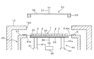
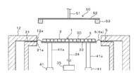
図2(a)の符号11は角筒状のケーシング、12はフレーム押さえプレート、13は蓋体である。フレーム押さえプレート12はケーシング11の上部開口に配設され、ケーシング11と蓋体13との間に挟まれた状態で保持される。ケーシング11には、図1で示したテープ6を介してウェーハ1を支持するフレーム5(以下、ウェーハ付きフレーム7と称する)の挿入口を開閉するカバー11aが設けられている。
In FIG. 2A,
ケーシング11内の底部には、図2(b)および図3に示す保持ユニット20が配設されている。この保持ユニット20は、正方形状のフレーム保持台21と、フレーム保持台21を昇降させる複数のエアシリンダ22と、円板状のウェーハ保持テーブル(保持手段)30と、ウェーハ保持テーブル30を昇降させる昇降機構(拡張手段)40とを備えている。
A holding
フレーム保持台21と上記フレーム押さえプレート12には、径がフレーム5の内径とほぼ同等の円形状の孔21a、12aが、それぞれ互いに同心状に形成されている。フレーム保持台21の孔21aの周囲の上面に、上記ウェーハ付きフレーム7のフレーム5が同心状に載置される。エアシリンダ22はケーシング11の底部に支持されており、上下方向に伸縮するピストンロッド22aの先端が、フレーム保持台21の下面に固定されている。
Circular holes 21 a and 12 a having a diameter substantially equal to the inner diameter of the
フレーム保持台21は、エアシリンダ22のピストンロッド22aが縮小した状態では、図3に示すように、フレーム押さえプレート12より下方のワーク受け取り位置に位置付けられる。上記ケーシング11のカバー11aを開けて上記挿入口からケーシング11内に挿入されるウェーハ付きフレーム7は、ワーク受け取り位置に位置付けられたフレーム保持台21にフレーム5が載置される。また、ピストンロッド22aが伸びるとフレーム保持台21は上昇し、図4に示すように、フレーム5がフレーム保持台21とフレーム押さえプレート12との間に挟まれ、固定される。このようにフレーム5がフレーム保持台21とフレーム押さえプレート12との間に挟まれ固定される位置が、ウェーハ付きフレーム7の待機位置とされる。
When the
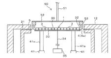
ウェーハ保持テーブル30は、フレーム保持台21の孔21aよりも小径で、この孔21aと同心状に配設されている。ウェーハ保持テーブル30は、ステンレス等からなる中実材料で円板状に形成されたもので、その上面31に、テープ6を介してウェーハ1が同心状に載置される。ウェーハ保持テーブル30の外径はウェーハ1よりも大きく、したがって図9に示すように、ウェーハ保持テーブル30の上面31に同心状に載置されたウェーハ1の外縁とウェーハ保持テーブル30の外縁との間には、テープ6の上記弛み領域6aのみで覆われる環状面31aが形成される。そして、この環状面31aには、図9および図10に示すように、環状の保持溝(保持部)32が全周にわたって形成されている。
The wafer holding table 30 has a smaller diameter than the
図3に示すように、ウェーハ保持テーブル30の内部には、保持溝32に連通して下面の中心に開口する空気通路33が形成されており、この空気通路33の開口には、配管34を介して、空気を吸引する真空ポンプ等からなる吸引源35が接続されている。吸引源35が運転されると保持溝32内が負圧となり、保持溝32を覆っているテープ6の弛み領域6aの一部が、全周にわたって保護溝32に吸着して保持されるようになっている。
As shown in FIG. 3, an
昇降機構40は、図3に示すように、複数のエアシリンダ41を備えており、これらエアシリンダ41の上下方向に伸縮するピストンロッド41aの先端が、ウェーハ保持テーブル30の下面に固定されている。ウェーハ保持テーブル30は、エアシリンダ41のピストンロッド41aが縮小した状態では、図3に示すように、ワーク受け取り位置でフレーム保持台21に載置されるウェーハ付きフレーム7より下方に位置付けられる。また、ピストンロッド41aが伸びるとウェーハ保持テーブル30が上昇してフレーム保持台21の孔を通過し、図5に示すように、ウェーハ付きフレーム7のウェーハ1およびテープ6がフレーム押さえプレート12の孔12a内に位置する拡張位置まで上昇させられる。
As shown in FIG. 3, the elevating
図2(b)および図3に示すように、フレーム押さえプレート12の上方には、ヒータユニット50が、フレーム押さえプレート12の孔12aと同心状に配設されている。このヒータユニット50は、蓋体13の下面に伸縮自在に設けられた上下方向に延びるロッド51の下端に、円板状のフランジ52が固定され、このフランジ52の下面の外周部に、環状のヒータ(外的刺激付与手段)53が固定されたものである。
As shown in FIGS. 2B and 3, the
ヒータ53は、フレーム保持台21およびウェーハ保持テーブル30に保持されたウェーハ付きフレーム7におけるテープ6の上記弛み領域6aに対応して、該弛み領域6aの上方に配設されている。また、ヒータ53は、弛み領域6aとほぼ同等の寸法を有しているが、その外径は、フレーム押さえプレート12の孔の径よりもやや小さい。ヒータ53は、例えば赤外線を下方に向けて照射して加熱する形式のものが好適に用いられる。
The
ヒータ53は、ロッド51が縮小した状態では、図3に示すようにフレーム押さえプレート12より上方に位置付けられる。そして、ロッド51が下方に伸びると、図7に示すようにフレーム押さえプレート12の孔12aの直上の加熱位置まで下降させられる。図7に示すように、ウェーハ付きフレーム7が上記拡張位置まで上昇した状態でヒータ53が加熱位置に位置付けられ、そのヒータ53がONされると、ヒータ53によってテープ6の弛み領域6aが所定温度に加熱されるようになっている。
When the
[3]テープ拡張装置の動作
次に、上記テープ拡張装置10の動作を説明する。この動作中に、本発明のテープ拡張方法が含まれている。
[3] Operation of Tape Expansion Device Next, the operation of the
動作前においては、図3に示すように、フレーム保持台21とウェーハ保持テーブル30はともに下降しており、ヒータ53は上方に位置付けられている。上記ケーシング11のカバー11aを開けて上記挿入口からウェーハ付きフレーム7をケーシング11内に挿入し、図3に示すように、フレーム5をフレーム保持台21に載置する。次に、図4に示すように、エアシリンダ22のピストンロッド22aが伸びてフレーム保持台21が上昇し、フレーム5がフレーム保持台21とフレーム押さえプレート12との間に挟まれ、ウェーハ付きフレーム7が待機位置に固定される。
Before the operation, as shown in FIG. 3, the frame holding table 21 and the wafer holding table 30 are both lowered, and the
次に、昇降機構40のエアシリンダ41のピストンロッド41aが伸び、ウェーハ保持テーブル30が、フレーム保持台21の孔21aを通過しながら上昇してウェーハ1の下側部分のテープ6に当接し、さらにウェーハ保持テーブル30が上昇して、図5に示すようにウェーハ保持テーブル30上のウェーハ1およびテープ6が上記拡張位置に位置付けられる(テープ拡張工程)。
Next, the
拡張位置に達する過程において、ウェーハ1の裏面に貼着されているテープ6は放射方向に引っ張られる力を受けて拡張する。そしてテープ6が放射方向に拡張するに伴い、ウェーハ1は、ダイシング加工が施されている分割予定ライン2に沿って分断され、個々のチップ3に分割される。また、ウェーハ1の裏面に貼着されているDAF4も、個々のチップ3に貼着した状態で、チップ3ごとに破断される。したがってテープ6上には、多数のDAF付きのチップ3が貼着しており、隣接するチップ3およびDAF4の間には、テープ6の拡張によって隙間が空いた状態となっている。
In the process of reaching the expansion position, the
図10の平面図および(a)の断面図はその状態を示しており、これら図で示すように、テープが拡張された状態で、弛み領域6aは保持溝32を覆っている。なお、図10の平面図ではウェーハ保持テーブル30の外縁は、本来ならばテープ6で覆われているため破線で示すべきであるが、保持溝32を明示するため、あえて実線で描いている。
The plan view of FIG. 10 and the cross-sectional view of FIG. 10A show this state. As shown in these drawings, the
テープ6を拡張してウェーハ1が多数のチップ3に分割されたら、引き続きウェーハ保持テーブル30の位置を保持してテープ6の拡張状態を確保した状態で、吸引源35を運転する。吸引源35が運転されると、テープ6の上記弛み領域6aの、保持溝32を覆っている環状部分が保持溝32に吸着して保持され、この環状の保持部分6bの内側であってチップ3が貼着されている部分のテープ6は、拡張状態が保持される(テープ保持工程)。
When the
次に、図6に示すようにウェーハ保持テーブル30が下降して、多数のチップ3が貼着しているテープ6が待機位置に戻る。待機位置に戻ったテープ6における弛み領域6aの上記保持部分6bよりも外側部分は、図10(b)に示すように、拡張して伸びたことにより弛みが生じている。次いで、ヒータユニット50を下降させて図7および図10(b)に示すようにヒータ53を弛み領域6aの直上に近接させ、ヒータ53をONして弛み領域6aを加熱する。ヒータ53によって加熱された弛み領域6aは、図8および図10(c)に示すように収縮する(テープ収縮工程)。
Next, as shown in FIG. 6, the wafer holding table 30 is lowered, and the
テープ6の弛み領域6aが十分に収縮する所定加熱時間が経過したら、ヒータ53をOFFにしてヒータユニット50を上昇させ、また、吸引源35の運転を停止する。吸引源35が停止しても、テープ6の保持部分6bよりも外側の弛み領域6aが収縮しているので、保持部分6bの内側の拡張状態はそのまま保持され、チップ3間の間隔は確保される。
When a predetermined heating time for sufficiently contracting the
次いで、ウェーハ保持テーブル30とフレーム保持台21を下降させてフレーム5および多数のチップ3が貼着されているテープ6をワーク受け取り位置に戻す。そして、上記挿入口からフレーム5がケーシング11外に出されて多数のチップ3が貼着された状態のテープ6が搬出され、この後は、DAF付きチップをテープ6から剥離する工程に移される。
Next, the wafer holding table 30 and the frame holding table 21 are lowered, and the
[4]実施形態の作用効果
上記実施形態によれば、上記テープ保持工程において、テープ6の弛み領域6aの一部を保持溝32に吸着して保持することにより、上記テープ収縮工程では、弛み領域6aの、保持溝32による保持部分6bよりも外側部分のみが収縮し、内側部分は収縮せず拡張状態が保持される。このため、ヒータ53の加熱によって収縮しやすい外周寄りのチップ3間の間隔も拡張状態が保持され、すなわち全てのチップ3間の間隔が保持される。その結果、テープ6の弛みに起因するチップ3どうしの接触に伴うチップ3の破損や、破断されたDAF4どうしの接合といった不具合の発生が防止される。
[4] Effect of Embodiment According to the above embodiment, in the tape holding step, a portion of the
なお、上記実施形態では、テープ6の弛み領域6aの一部をウェーハ保持テーブル30に保持する保持部を、テープ6を吸着して保持する保持溝32で構成しているが、本発明に係る保持部はこのような形態に限られない。例えば、弛み領域6aを上から押さえ付けてウェーハ保持テーブル30との間に挟み込んで固定する環状の固定部材を上下動可能に設けるなどの手段を採用してもよい。
In the above embodiment, the holding portion that holds a part of the
1…半導体ウェーハ(ワーク)、3…半導体チップ、3a…製品チップ、3b…余剰チップ、5…フレーム、5a…フレームの開口部、6…粘着テープ、6a…弛み領域、10…テープ拡張装置、30…ウェーハ保持テーブル(保持手段)、32…保持溝(保持部)、40…昇降機構(拡張手段)、53…ヒータ(外的刺激付与手段)。
DESCRIPTION OF
Claims (2)
保持手段に載置した前記テープを、待機位置から、該テープを拡張する拡張位置に位置付けて拡張するテープ拡張工程と、
該テープを前記拡張位置に位置付けて拡張した状態で、前記弛み領域の一部を、前記保持手段に形成した保持溝に吸着して全周にわたって保持し、該テープの該保持溝に吸着された部分の内側を拡張状態に保持するテープ保持工程と、
該テープを、前記待機位置に位置付けて前記弛み領域を弛ませた状態としてから、該弛み領域に外的刺激を付与してテープを収縮させるテープ収縮工程と、を含むことを特徴とするテープ拡張方法。 After extending a tape that is attached to an annular frame and a work on which a plurality of chips disposed in the opening of the frame are formed and supports the work on the frame, an inner edge of the frame on the tape A tape expansion method for contracting a slack area between the outer edge of the workpiece,
A tape expansion step of expanding the tape placed on the holding means from a standby position at an expansion position for expanding the tape; and
In a state where the tape is expanded at the extended position, a part of the slack area is adsorbed to the holding groove formed in the holding means and held around the entire circumference, and is adsorbed to the holding groove of the tape . A tape holding process for holding the inside of the part in an expanded state;
A tape expansion step comprising: a tape contracting step of positioning the tape at the standby position to relax the slack area, and then contracting the tape by applying an external stimulus to the slack area. Method.
前記テープを保持可能な保持手段と、
該保持手段に載置された前記テープを、待機位置から、該テープを拡張する拡張位置に位置付けて拡張する拡張手段と、
前記テープの前記弛み領域に外的刺激を付与する外的刺激付与手段と、を有し、
前記保持手段は、前記拡張手段によって前記テープを前記拡張位置に位置付けて拡張した状態で、前記弛み領域の一部を全周にわたって保持し、該テープの保持された部分の内側を拡張状態に保持する保持部を有し、該保持部は、前記保持手段に形成され、吸引源に連通する保持溝であって、該保持溝に前記テープの前記弛み領域の前記一部を吸着作用によって保持することを特徴とするテープ拡張装置。 The tape is attached to a ring-shaped frame and a work on which a large number of chips arranged in the opening of the frame are formed, and the tape that supports the work on the frame is expanded, and then the inner edge of the frame on the tape A tape expansion device for contracting a slack area between the outer edge of the workpiece,
Holding means capable of holding the tape;
Expansion means for positioning and expanding the tape placed on the holding means from a standby position to an expansion position for expanding the tape;
An external stimulus applying means for applying an external stimulus to the slack area of the tape,
The holding means holds a part of the slack area over the entire circumference in a state where the tape is expanded by the expansion means being positioned at the extended position, and holds the inside of the held part of the tape in the expanded state. a holding unit which possess, the holding portion is formed in the holding means, a retaining groove which communicates with the suction source, is held by the suction action of the part of the slack region of the tape by the holding groove A tape expansion device characterized by that.
Priority Applications (1)
| Application Number | Priority Date | Filing Date | Title |
|---|---|---|---|
| JP2008324134A JP5378780B2 (en) | 2008-12-19 | 2008-12-19 | Tape expansion method and tape expansion device |
Applications Claiming Priority (1)
| Application Number | Priority Date | Filing Date | Title |
|---|---|---|---|
| JP2008324134A JP5378780B2 (en) | 2008-12-19 | 2008-12-19 | Tape expansion method and tape expansion device |
Publications (2)
| Publication Number | Publication Date |
|---|---|
| JP2010147317A JP2010147317A (en) | 2010-07-01 |
| JP5378780B2 true JP5378780B2 (en) | 2013-12-25 |
Family
ID=42567412
Family Applications (1)
| Application Number | Title | Priority Date | Filing Date |
|---|---|---|---|
| JP2008324134A Active JP5378780B2 (en) | 2008-12-19 | 2008-12-19 | Tape expansion method and tape expansion device |
Country Status (1)
| Country | Link |
|---|---|
| JP (1) | JP5378780B2 (en) |
Cited By (1)
| Publication number | Priority date | Publication date | Assignee | Title |
|---|---|---|---|---|
| KR20180133789A (en) * | 2017-06-07 | 2018-12-17 | 가부시기가이샤 디스코 | Wafer dividing method and wafer dividing apparatus |
Families Citing this family (10)
| Publication number | Priority date | Publication date | Assignee | Title |
|---|---|---|---|---|
| KR101843794B1 (en) | 2011-02-16 | 2018-03-30 | 가부시키가이샤 토쿄 세이미쯔 | Work dividing device and method for dividing work |
| JP5854215B2 (en) * | 2011-02-16 | 2016-02-09 | 株式会社東京精密 | Work dividing apparatus and work dividing method |
| JP5013148B1 (en) * | 2011-02-16 | 2012-08-29 | 株式会社東京精密 | Work dividing apparatus and work dividing method |
| JP5981154B2 (en) * | 2012-02-02 | 2016-08-31 | 三菱電機株式会社 | Manufacturing method of semiconductor device |
| JP6295135B2 (en) * | 2014-04-24 | 2018-03-14 | 日東電工株式会社 | Dicing die bond film |
| JP6266429B2 (en) * | 2014-05-08 | 2018-01-24 | 株式会社ディスコ | Chip interval maintaining device and chip interval maintaining method |
| JP6320198B2 (en) * | 2014-06-27 | 2018-05-09 | 株式会社ディスコ | Tape expansion unit |
| JP6741529B2 (en) | 2016-09-09 | 2020-08-19 | 株式会社ディスコ | Tip spacing maintenance method |
| JP6376363B2 (en) * | 2016-11-10 | 2018-08-22 | 株式会社東京精密 | Work dividing device |
| JP7436772B2 (en) | 2018-12-27 | 2024-02-22 | 日亜化学工業株式会社 | Manufacturing method of semiconductor device |
Family Cites Families (2)
| Publication number | Priority date | Publication date | Assignee | Title |
|---|---|---|---|---|
| JP4288392B2 (en) * | 2003-09-29 | 2009-07-01 | 株式会社東京精密 | Expanding method |
| JP5354149B2 (en) * | 2008-04-08 | 2013-11-27 | 株式会社東京精密 | Expanding method |
-
2008
- 2008-12-19 JP JP2008324134A patent/JP5378780B2/en active Active
Cited By (2)
| Publication number | Priority date | Publication date | Assignee | Title |
|---|---|---|---|---|
| KR20180133789A (en) * | 2017-06-07 | 2018-12-17 | 가부시기가이샤 디스코 | Wafer dividing method and wafer dividing apparatus |
| KR102448225B1 (en) | 2017-06-07 | 2022-09-27 | 가부시기가이샤 디스코 | Wafer dividing method and wafer dividing apparatus |
Also Published As
| Publication number | Publication date |
|---|---|
| JP2010147317A (en) | 2010-07-01 |
Similar Documents
| Publication | Publication Date | Title |
|---|---|---|
| JP5378780B2 (en) | Tape expansion method and tape expansion device | |
| US7648850B2 (en) | Method for producing semiconductor chip | |
| JP6958924B2 (en) | How to process a wafer | |
| TWI438834B (en) | Method of dividing an adhesive film bonded to a wafer | |
| JP6962523B2 (en) | Wafer processing method | |
| JP7056844B2 (en) | Wafer processing method | |
| JP5253996B2 (en) | Work dividing method and tape expansion device | |
| US9576835B2 (en) | Workpiece processing method | |
| US11315833B2 (en) | Wafer processing method including a test element group (TEG) cutting step | |
| KR102250216B1 (en) | Wafer processing method | |
| WO2004038779A1 (en) | Expansion method and device | |
| TWI703625B (en) | Wafer processing method | |
| JP2017103405A (en) | Wafer processing method | |
| US10580697B2 (en) | Workpiece dividing method | |
| JP2015216151A (en) | Chip spacing preserving device and chip spacing preserving method | |
| JP2010147316A (en) | Method and apparatus for expanding tape | |
| JP2004193241A (en) | Dividing method of semiconductor wafer | |
| JP6033116B2 (en) | Laminated wafer processing method and adhesive sheet | |
| JP6298699B2 (en) | Wafer processing method | |
| JP6457223B2 (en) | Substrate separation method and semiconductor manufacturing apparatus | |
| JP2008135513A (en) | Tape expanding device | |
| KR102181999B1 (en) | Expanded sheet, producing method for expanded sheet, and expanding method for expanded sheet | |
| JP2018067678A (en) | Chip interval maintenance method | |
| JP2002353296A (en) | Equipment for peeling wafer protective tape and wafer mounting equipment | |
| JP2020129642A (en) | Expanding sheet expansion method |
Legal Events
| Date | Code | Title | Description |
|---|---|---|---|
| A621 | Written request for application examination |
Free format text: JAPANESE INTERMEDIATE CODE: A621 Effective date: 20111111 |
|
| A131 | Notification of reasons for refusal |
Free format text: JAPANESE INTERMEDIATE CODE: A131 Effective date: 20130325 |
|
| A977 | Report on retrieval |
Free format text: JAPANESE INTERMEDIATE CODE: A971007 Effective date: 20130327 |
|
| A521 | Request for written amendment filed |
Free format text: JAPANESE INTERMEDIATE CODE: A523 Effective date: 20130524 |
|
| TRDD | Decision of grant or rejection written | ||
| A01 | Written decision to grant a patent or to grant a registration (utility model) |
Free format text: JAPANESE INTERMEDIATE CODE: A01 Effective date: 20130902 |
|
| A61 | First payment of annual fees (during grant procedure) |
Free format text: JAPANESE INTERMEDIATE CODE: A61 Effective date: 20130926 |
|
| R150 | Certificate of patent or registration of utility model |
Ref document number: 5378780 Country of ref document: JP Free format text: JAPANESE INTERMEDIATE CODE: R150 Free format text: JAPANESE INTERMEDIATE CODE: R150 |
|
| R250 | Receipt of annual fees |
Free format text: JAPANESE INTERMEDIATE CODE: R250 |
|
| R250 | Receipt of annual fees |
Free format text: JAPANESE INTERMEDIATE CODE: R250 |
|
| R250 | Receipt of annual fees |
Free format text: JAPANESE INTERMEDIATE CODE: R250 |
|
| R250 | Receipt of annual fees |
Free format text: JAPANESE INTERMEDIATE CODE: R250 |
|
| R250 | Receipt of annual fees |
Free format text: JAPANESE INTERMEDIATE CODE: R250 |
|
| R250 | Receipt of annual fees |
Free format text: JAPANESE INTERMEDIATE CODE: R250 |
|
| R250 | Receipt of annual fees |
Free format text: JAPANESE INTERMEDIATE CODE: R250 |
|
| R250 | Receipt of annual fees |
Free format text: JAPANESE INTERMEDIATE CODE: R250 |