JP2004088083A - Semiconductor light emitting device, its manufacturing method, and its packaging method - Google Patents
Semiconductor light emitting device, its manufacturing method, and its packaging method Download PDFInfo
- Publication number
- JP2004088083A JP2004088083A JP2003175716A JP2003175716A JP2004088083A JP 2004088083 A JP2004088083 A JP 2004088083A JP 2003175716 A JP2003175716 A JP 2003175716A JP 2003175716 A JP2003175716 A JP 2003175716A JP 2004088083 A JP2004088083 A JP 2004088083A
- Authority
- JP
- Japan
- Prior art keywords
- semiconductor
- film
- laminated film
- electrode
- light emitting
- Prior art date
- Legal status (The legal status is an assumption and is not a legal conclusion. Google has not performed a legal analysis and makes no representation as to the accuracy of the status listed.)
- Pending
Links
Images


Landscapes
- Led Devices (AREA)
Abstract
Description
【0001】
【発明の属する技術分野】
本発明は、短波長発光ダイオード素子等の半導体発光素子、その製造方法及びその実装方法に関する。
【0002】
【従来の技術】
一般式がBzAlxGa1−x−y−zInyN1−v−wAsvPw(但し、x,y,z,v,wは、0≦x≦1,0≦y≦1,0≦z≦1,0≦x+y+z≦1,0≦v≦1,0≦w≦1,0≦v+w≦1である。)で表わされるIII−V族窒化物半導体(一般にBAlGaInNAsPで表記され、以下、GaN系半導体と呼ぶ。)は、例えば窒化ガリウム(GaN)の場合には、室温における禁制帯幅が3.4eVと比較的に広い禁制帯幅を有しているため、青色光若しくは緑色光を出力する可視域発光ダイオード素子又は短波長半導体レーザ素子等の発光デバイスや、高温下での動作が可能なトランジスタ又は高速動作が可能な大電力トランジスタ等の幅広い応用が期待されている。発光デバイスは、発光ダイオード素子及び半導体レーザ素子が商品化されている。なかでも、発光ダイオード素子は、青色光又は緑色光を出力する各種表示装置、大型ディスプレイ装置及び交通信号機で実用化されている。また、蛍光材料が励起されて発光する白色発光ダイオード素子は、現行の蛍光灯や白熱灯を置き換える、いわゆる半導体照明の実現に向け、その高輝度化及び発光効率の改善を図って研究開発が活発に進められている。
【0003】
これまで、GaN系半導体は他のワイドギャップ半導体と同様に、結晶成長法による成長が困難であったが、最近になって有機金属気相成長(Metal Organic Chemical Vapor Deposition:MOCVD)法を中心とする結晶成長技術が大きく進展したため、前述の発光ダイオード素子が実用化されるに至っている。
【0004】
ところで、結晶成長層(エピタキシャル層)の成長用基板として、窒化ガリウム(GaN)からなる基板を作製することは容易ではなく、従って、シリコン(Si)又はヒ化ガリウム(GaAs)のように、基板自体への製造プロセスを行なえず、また基板上のエピタキシャル層も同一材料からなる基板上への成長を行なえないため、一般にはエピタキシャル層と異なる材料を基板に用いたヘテロエピタキシャル成長を行なっている。
【0005】
これまでに最も広く用いられ、最も優れたデバイス特性を示しているのがサファイアを基板として成長したGaN系半導体である。サファイアの結晶構造はGaN系半導体と同一の六方晶系であり、しかも熱的に極めて安定であるため、1000℃以上という高温を必要とされるGaN系半導体の結晶成長に適している。従って、従来は、主にサファイアからなる基板上に成長したGaN系半導体層に対して発光ダイオード素子の高輝度化及び発光効率の改善が図られてきた。例えば、高輝度化を図るには、GaN系半導体における結晶性を良好とし非発光再結合を抑制することにより内部量子効率を向上させることと、光の取り出し効率を改善することとの2点が重要である。
【0006】
前述したように、近年結晶成長技術が大いに進展した結果、内部量子効率の向上は限界に近づきつつあるため、最近では光の取り出し効率の向上が重要な課題となってきている。
【0007】
以下、従来の光の取り出し効率の改善を図る2つの手法について図面を参照しながら説明する。
【0008】
(第1の従来例)
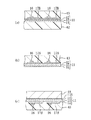
図18に示すように、第1の従来例に係る発光ダイオード素子は、例えばMOCVD法により、サファイアからなる基板101の上に、n型AlGaNからなるn型半導体層102と、InGaNからなる活性層103と、p型AlGaNからなるp型半導体層104とを順次成長する。続いて、ドライエッチングによりn型半導体層102の一部を選択的に露出し、露出したn型半導体層102の上に、Ti/Alからなるn側電極106を形成する。また、p型半導体層104の上には、厚さが10nm程度かそれ以下のNi/Auからなる透明p側電極107を形成し、透明p側電極107上の一部の領域にAlからなるボンディングパッド108を形成する(特許文献1参照)。
【0009】
このように、第1の従来例に係る発光ダイオード素子は、透明p側電極107を用いることにより、活性層103から出射される例えば波長が470nmの青色の発光光はその大部分が透明p側電極107を透過して外部へ取り出されるため、高輝度発光が可能である。それでも、基板101側への発光光は十分には取り出されないため、発光効率の改善には限界がある。
【0010】
(第2の従来例)
図19に示すように、第2の従来例に係る発光ダイオード素子は、保護ダイオード付きサブマウント113の上面に、p型半導体層104を対向させて実装する、いわゆるフリップチップ実装されてなり、サファイアからなる基板101を通して発光光を取り出している(特許文献2参照)。ここで、p型半導体層104のサブマウント113との対向面には、Niからなるp側電極110が形成されており、該p側電極110とサブマウント113との間、及びn側電極106とサブマウント113との間には、それぞれAgからなるバンプ111が形成されている。ここでは、サファイアからなる基板101が絶縁性材料であるため、静電耐圧が小さい。従って、サージ電圧が印加された場合に、サージ電流がチップを流れないように保護ダイオード付きのサブマウント113を用いている。
【0011】
また、バンプ111を構成するAgは青色光に対して高反射率を有するため、この高反射率を有する電極構造とフリップチップ実装とによって、活性層103からの例えば波長が470nmの青色の発光光はその大部分がバンプ111で反射された後に、基板101を透過して外部に取り出される。従って、高輝度発光が可能である。また、保護ダイオード付きサブマウント113を用いていることから、静電耐圧が大きくなっている。
【0012】
【特許文献1】
特開平07−94782号公報
【特許文献2】
特開平11−191641号公報
【特許文献3】
特開2001−274507号公報
【特許文献4】
特開2001−313422号公報
【0013】
【発明が解決しようとする課題】
しかしながら、前記第1の従来例及び第2の従来例に係る発光ダイオード素子は、そのいずれもがサファイアからなる基板101上に形成されており、サファイアは熱伝導性が比較的に低く放熱性が劣るため、高出力動作の限界点が低いという問題がある。
【0014】
また、サファイアは絶縁性であり静電耐圧が低いため、第2の従来例のようにサージ対策用の保護ダイオード素子を設ける必要がある等、実装コストが大きくなるという問題もある。
【0015】
さらに、基板101が導電性を持たないことから、n側電極とp側電極とを基板101に対して同一面(上面)側に形成する構成しか採り得ず、両電極を基板101を挟んで互いに対向するように設けることができない。その結果、ダイオード素子として直列抵抗が大きくなってしまい、動作電圧が大きくなるという問題がある。
【0016】
本発明は、前記従来の問題に鑑み、化合物半導体、特にGaN系半導体からなる半導体発光素子に対して、その放熱性を良好とすると共に静電耐圧を増大し、さらに発光効率の向上と直列抵抗の低減とを図ることを目的とする。
【0017】
【課題を解決するための手段】
前記の目的を達成するため、本発明は、半導体発光素子を、活性層を含む化合物半導体からなる半導体積層膜の表面及び裏面に互いに対向する対向電極を形成し、対向電極の一方に比較的に厚膜の金属膜を設ける構成とする。さらに、対向電極のうち金属膜と接する一方の電極材料には活性層からの発光光に対する反射率が高い材料を選択し、且つ他方の電極材料には透光性材料を選択するか又はその平面寸法を可能な限り小さくする。
【0018】
具体的には、本発明に係る半導体発光素子は、互いに異なる導電型を持つ少なくとも2つの半導体層を含む半導体積層膜と、半導体積層膜の一方の面上に形成された第1の電極と、半導体積層膜の一方の面と対向する対向面上に形成された第2の電極と、第1の電極又は第2の電極と接するように形成され、半導体積層膜の膜厚よりも大きいか等しい膜厚を有する金属膜とを備えている。
【0019】
本発明の半導体発光素子によると、互いに異なる導電型を持つ少なくとも2つの半導体層を含む半導体積層膜が成長した基板を除去し、代わりに、半導体積層膜の膜厚よりも大きいか等しい膜厚を有する金属膜を設けることにより、基板を残した場合における該基板による発光光の吸収を抑制できる。その結果、半導体積層膜における金属膜の反対側の面からより多くの発光光を取り出すことが可能となる。また、基板を除去して比較的厚膜の金属膜を設けるため、直列抵抗を低減できる上に、放熱性が大幅に改善され且つ静電耐圧が大きくなる。その上、金属膜と接する電極に高反射材料を用いた場合には発光効率を増大することが可能となる。
【0020】
本発明の半導体発光素子において、半導体積層膜はV族元素に窒素を含むIII−V族化合物半導体からなることが好ましい。このようにすると、V族元素に窒素を含むIII−V族化合物半導体、すなわちIII−V族窒化物半導体は、サファイア等の異種基板を用いる場合が多いため、該異種基板を除去する効果は極めて大きい。
【0021】
本発明の半導体発光素子において、金属膜の膜厚は10μm以上であることが好ましい。
【0022】
本発明の半導体発光素子において、金属膜は金、銅又は銀からなることが好ましい。このようにすると、金、銅及び銀はいずれも熱伝導率が大きいため、放熱性がより向上するので、さらなる大出力動作を確実に行なえるようになる。
【0023】
本発明の半導体発光素子において、金属膜はめっきにより形成されていることが好ましい。このようにすると、金属膜を短時間で且つ再現性良く形成できるため、高出力動作が可能な半導体発光素子を低コストで実現できる。
【0024】
本発明の半導体発光素子において、金属膜は、半導体積層膜の反対側部分に融点が300℃以下である金属層を含むことが好ましい。このようにすると、半導体発光素子をパッケージ又はリードフレームにダイスボンディングする場合に、融点が300℃以下の金属層は半田材として機能するため、わざわざ半田材を用いる必要がなくなるので、再現性良く且つ低コストで発光素子のダイスボンディングを行なうことができる。
【0025】
この場合に、金属層は錫を含むことが好ましい。
【0026】
本発明の半導体発光素子において、第1の電極及び第2の電極のうち金属膜と接するように形成された電極は、半導体積層膜から発光される光に対して90%以上の反射率を有していることが好ましい。このようにすると、光の取り出し効率が向上するため、発光素子の高輝度化を実現できる。
【0027】
本発明の半導体発光素子において、第1の電極及び第2の電極のうち金属膜と接するように形成された電極は、金、白金、銅、銀及びロジウムのうちの少なくとも1つからなる単層膜、又はこれらのうちの2つ以上を含む積層膜からなることが好ましい。このようにすると、半導体積層膜から発光される光に対して90%以上の反射率を有する電極を確実に形成することができる。
【0028】
本発明の半導体発光素子は、半導体積層膜と金属膜との間に形成され、誘電体又は半導体からなるミラー構造体をさらに備え、ミラー構造体は、半導体積層膜から発光される光に対して90%以上の反射率を有していることが好ましい。このようにすると、ミラー構造体は、反射率が大きい単体の材料からなる電極と比べて光の取り出し効率が高いため、発光素子の高輝度化を実現できる。
【0029】
この場合に、ミラー構造体は、酸化シリコン、酸化チタン、酸化ニオブ、酸化タンタル及び酸化ハフニウムのうちのいずれか、又は窒化アルミニウムガリウムインジウム(AlxGayIn1−x−y N)(但し、0≦x、y≦1、0≦x+y≦1である。)を含み、半導体積層膜からの発光波長に対する屈折率が周期的に変化するように形成されていることが好ましい。このようにすると、ミラー構造体を構成する各層ごとの屈折率差が大きくなるため、層数を減らしても反射率が大きいミラー構造体を得ることができる。
【0030】
本発明の半導体発光素子において、第1の電極及び第2の電極のうち半導体積層膜に対して金属膜の反対側に設けられた電極は、透光性を有していることが好ましい。このようにすると、半導体積層膜から発光される発光光が透光性を有する電極を通して取り出されるので、光の取り出し効率が改善される。
【0031】
また、本発明の半導体発光素子において、第1の電極及び第2の電極のうち半導体積層膜に対して金属膜の反対側に設けられた電極は、インジウム錫酸化物からなるか、又は膜厚が20nm以下のニッケルを含む金属からなることが好ましい。このようにすると、透光性を有する電極を確実に形成することができる。
【0032】
本発明の半導体発光素子は、半導体積層膜と金属膜との間で且つその側部に形成され、誘電体からなる電流狭窄膜をさらに備えていることが好ましい。
【0033】
本発明に係る半導体発光素子の製造方法は、単結晶からなる基板上に、互いに異なる導電型を持つ少なくとも2つの半導体層を含む半導体積層膜を形成する工程(a)と、基板を半導体積層膜から分離する工程(b)と、半導体積層膜の一方の面上に第1の電極を形成し、半導体積層膜の一方の面と対向する対向面上に第2の電極を形成する工程(c)と、第1の電極及び第2の電極のうちの一方の上に金属膜を形成する工程(d)とを備えている。
【0034】
本発明の半導体発光素子の製造方法によると、基板上に互いに異なる導電型を持つ少なくとも2つの半導体層を含む半導体積層膜を形成し、続いて基板を半導体積層膜から分離した後、半導体積層膜の一方の面上に第1の電極を形成し、半導体積層膜の一方の面と対向する対向面上に第2の電極を形成し、さらに第1の電極及び第2の電極のうちの一方の上に金属膜を形成する。このように、半導体積層膜を形成した基板を半導体積層膜から分離するため、基板による発光光の吸収を抑制できるので、半導体積層膜における金属膜と反対側の面側からより多くの発光光を取り出すことができるようになる。また、基板に代えて半導体積積層膜の上に電極を介在させて金属膜を設けるため、半導体積層膜における直列抵抗を低減できる上に、放熱性を大幅に改善でき且つ静電耐圧が大きくなる。
【0035】
本発明の半導体発光素子の製造方法において、半導体積層膜はV族元素に窒素を含むIII−V族化合物半導体からなることが好ましい。
【0036】
本発明の半導体発光素子の製造方法は、工程(b)において、基板における半導体積層膜の反対側の面から、基板を透過し且つ半導体積層膜の一部に吸収される波長を有する照射光を照射して、半導体積層膜の内部に半導体積層膜の一部が分解してなる分解層を形成することにより、基板を半導体積層膜から分離することが好ましい。このようにすると、基板の面積が比較的に大きい場合であっても、基板と半導体積層膜とを再現性良く分離することができる。
【0037】
また、本発明の半導体発光素子の製造方法は、工程(b)において基板を研磨により除去することにより、基板を半導体積層膜から分離することが好ましい。このようにすると、基板の面積が比較的に大きい場合であっても、低コストで半導体積層膜を分離することができる。
【0038】
本発明の半導体発光素子の製造方法において、工程(a)は、半導体積層膜の一部を形成した後、基板における半導体積層膜の反対側の面から、基板を透過し且つ半導体積層膜に吸収される波長を有する照射光を照射することにより、半導体積層膜の一部の内部に半導体積層膜が分解してなる分解層を形成する工程と、分解層を形成した後、半導体積層膜の一部の上に半導体積層膜の残部を形成する工程とを含むことが好ましい。このようにすると、半導体積層膜と基板とは、該半導体積層膜の一部が分解してなる分解層を介在させて緩やかに結合されるようになる。このため、分解層を形成した後に、半導体積層膜の一部の上に半導体積層膜の残部を形成すると、半導体積層膜の残部に例えばデバイス構造(活性層)を含む場合には、基板と半導体積層膜との間の熱膨張係数の差や格子不整合の影響を受け難くなるので、デバイス構造の結晶性が良好となり、高輝度の半導体発光素子を得ることが可能となる。
【0039】
基板に照射する照射光はパルス状に発振するレーザ光であることが好ましい。また、照射光は水銀ランプの輝線であることが好ましい。このようにすると、光源にパルス状に発振するレーザ光を用いた場合には、光の出力パワーを著しく増大させることができるため、半導体積層膜の分離が容易となる。また、光源に水銀ランプの輝線を用いた場合には、光の出力パワーではレーザ光に劣るものの、スポットサイズをレーザ光の場合よりも大きくできるため、照射工程におけるスループットが向上する。
【0040】
また、照射光は基板の面内をスキャンするように照射することが好ましい。このようにすると、比較的に面積が大きい基板であっても、光源のビームサイズに影響されることなく半導体積層膜から基板を分離することができる。
【0041】
また、照射光は基板を加熱しながら照射することが好ましい。このようにすると、結晶成長後の冷却時に生じる半導体積層膜と基板との熱膨張係数の差、及び両者の格子不整合による半導体積層膜中に生じるストレスが緩和されるため、基板を分離する際に半導体積層膜に生じるクラックを防止することができる。
【0042】
本発明の半導体発光素子の製造方法は、工程(a)と工程(b)との間に、半導体積層膜の上に誘電体又は半導体からなる積層膜を形成した後、形成した積層膜をパターニングする工程(e)をさらに備え、工程(c)において、第1の電極及び第2の電極のうちのいずれか一方を、パターニングされた積層膜の上に形成し、工程(d)において、金属膜はパターニングされた積層膜の上に形成した電極の上に形成することが好ましい。このようにすると、半導体積層膜から発光される発光光を高効率で反射するミラー構造体を形成することができる。その上、一般に低抵抗化が困難である誘電体又は半導体からなる積層膜により構成されるミラー構造体をパターニングするため、パターニングされたミラー構造体同士の隙間に電極及び金属膜が形成されるので、その隙間から十分な動作電流を確実に注入することができる。
【0043】
この場合に、工程(c)において、基板を半導体積層膜から分離した後に、第1の電極及び第2の電極のうちの他方を、半導体積層膜における積層膜の反対側の面上に形成することが好ましい。
【0044】
本発明の半導体発光素子の製造方法は、工程(a)と工程(b)との間に、半導体積層膜を構成する材料と異なる材料からなり、半導体積層膜を保持する膜状の第1の保持部材を半導体積層膜に貼り合わせる工程(f)と、工程(b)よりも後に、第1の保持部材を半導体積層膜から剥離する工程(g)とをさらに備えていることが好ましい。このようにすると、半導体積層膜の一部に分解層を形成する際における膜中のストレスの緩和過程で、半導体積層膜に発生するクラックを抑制することができる。その結果、基板の面積が比較的に大きい場合であっても、半導体積層膜にクラックを発生させることなく基板を分離することができる。
【0045】
この場合に、本発明の半導体発光素子の製造方法は、工程(g)の前に、第1の保持部材とは特性が異なる膜状の第2の保持部材を、半導体積層膜における第1の保持部材の反対側の面上に貼り合わせる工程(h)と、工程(g)よりも後に、第2の保持部材を半導体積層膜から剥離する工程(i)とをさらに備えていることが好ましい。このようにすると、半導体積層膜から基板を分離した後でも、半導体積層膜の任意の面上への電極形成や金属膜に対するパターニングが可能となる。
【0046】
また、この場合に、第1の保持部材又は第2の保持部材は、高分子材料フィルム、半導体からなる単結晶基板又は金属板であることが好ましい。このようにすると、高分子材料フィルム又は金属板の場合には可塑性に優れ、半導体からなる単結晶基板の場合には劈開性に優れるため、基板の分離をより容易に行なえる。
【0047】
この場合の高分子材料フィルムは、その貼り合わせ面に加熱により剥離可能な接着材層が設けられていることが好ましい。このようにすると、高分子材料フィルムを剥離する際に、半導体積層膜上に接着材層が残留するという不具合がなくなるため、半導体積層膜からの高分子材料フィルムの剥離を容易に且つ確実に行なえるようになる。
【0048】
本発明の半導体発光素子の製造方法は、工程(c)よりも前に、半導体積層膜の上に誘電体からなる電流狭窄膜を選択的に形成する工程(j)をさらに備えていることが好ましい。
【0049】
本発明に係る半導体発光素子の実装方法は、単結晶からなる基板上に、互いに異なる導電型を持つ少なくとも2つの半導体層を含む半導体積層膜を形成する工程(a)と、半導体積層膜を構成する材料と異なる材料からなり、半導体積層膜を保持する膜状の保持部材を半導体積層膜に貼り合わせる工程(b)と、半導体積層膜を保持部材と共にダイシングを行なって、それぞれ個辺化された保持部材に保持された状態の複数のチップを作製する工程(c)と、保持部材に保持された各チップに対してダイスボンディングを行なった後、保持部材を各チップから剥離する工程(d)とを備えている。
【0050】
本発明の半導体発光素子の実装方法によると、半導体積層膜の膜厚が例えば数μm以下と極めて小さい場合でも、膜状の保持部材を半導体積層膜に貼った状態でダイスボンディングを行なえるため、極めて薄い半導体発光素子を実装することが可能となる。
【0051】
本発明の半導体発光素子の実装方法において、保持部材は、高分子材料フィルムであることが好ましい。
【0052】
本発明の半導体発光素子の実装方法において、高分子材料フィルムは、その貼り合わせ面に加熱により剥離可能な接着材層が設けられていることが好ましい。
【0053】
【発明の実施の形態】
(第1の実施形態)
本発明の第1の実施形態について図面を参照しながら説明する。
【0054】
図1は本発明の第1の実施形態に係る半導体発光素子であって、青色又は緑色等の短波長発光が可能な発光ダイオード素子の断面構成を示している。
【0055】
図1に示すように、第1の実施形態に係る発光ダイオード素子10は、複数の半導体層を含む素子構造体11を有している。
【0056】
素子構造体11の上にはインジウム(In)と錫(Sn)とを含む酸化物(ITO)からなる透光性を有するp側電極15が形成され、該p側電極15の上の一部の領域には金(Au)からなるボンディングパッド16が形成され、また、素子構造体11におけるp側電極15の反対側の面上にはチタン(Ti)と金(Au)との積層体からなるn側電極17が形成されている。
【0057】
素子構造体11は、n型の窒化アルミニウムガリウム(AlGaN)からなるn型半導体層12と、該n型半導体層12の上に形成された窒化インジウムガリウム(InGaN)からなる活性層13と、該活性層13の上に形成されたp型の窒化アルミニウムガリウム(AlGaN)からなるp型半導体層14とから構成されている。ここで、活性層13は例えば量子井戸構造を有していても良い。活性層13において生成された例えば波長が470nmの青色発光光は、Ti/Auからなるn側電極17により反射され、ITOからなるp側電極15を透過して外部に取り出される。
【0058】
第1の実施形態の特徴として、n側電極17におけるn型半導体層12の反対側(下側)のAu層を下地層として、厚さが約50μmの金めっきによる金属膜18が形成されている。
【0059】
このように、第1の実施形態によると、発光ダイオード素子10を構成する素子構造体11のn型半導体層12に、活性層13からの発光光に対する反射率が90%以上となるように設けられた金属からなるn側電極17が形成されている。これにより、活性層13から出射される発光光はn側電極17により反射され、透光性を有するp側電極15を通して取り出されるため、光の取り出し効率を大幅に向上することができる。
【0060】
その上、n側電極17における素子構造体11の反対側の面上には、単結晶からなる基板に代えてAuからなる金属膜18を設けているため、活性層13で生じた熱は金属膜18を介して外部に放熱される。このように、GaN系半導体からなる素子構造体11を成長させる単結晶基板に代えて金属膜18を設けていることにより、素子構造体11の放熱性が格段に向上するため、本実施形態に係る発光ダイオード素子10は高出力動作を確実に行なえるようになる。また、サファイアのような絶縁性基板を有さないため、静電耐圧性も向上する。
【0061】
なお、金属膜18の厚さは10μm以上であれば良く、またその材料も金(Au)に限られない。例えば、銅(Cu)又は銀(Ag)のような熱伝導率が高い材料であれば良く、またこれらの合金でもよい。
【0062】
また、金属膜18と接するn側電極17は、チタン(Ti)と金(Au)との積層構造に限られず、金(Au)、白金(Pt)、銅(Cu)、銀(Ag)及びロジウム(Rh)のうちの少なくとも1つからなる単層膜、又はこれらのうちの2つ以上を含む積層構造としても良い。
【0063】
また、透光性を有するp側電極15はITOに限られず、ニッケル(Ni)と金(Au)とからなり、併せた厚さが20nm以下の積層体を用いてもよい。
【0064】
以下、前記のように構成された発光ダイオード素子10の製造方法について図面を参照しながら説明する。
【0065】
図2(a)〜図2(d)及び図3(a)〜図3(d)は本発明の第1の実施形態に係る発光ダイオード素子の製造方法の工程順の断面構成を示している。
【0066】
まず、図2(a)に示すように、例えば有機金属気相成長(MOCVD)法により、ウエハ状のサファイア(単結晶Al2O3)からなる基板20の主面上に、n型AlGaNからなるn型半導体層12、InGaNからなる活性層13及びp型AlGaNからなるp型半導体層14を順次成長することにより、n型半導体層12、活性層13及びp型半導体層14を含む素子構造体11を形成する。
【0067】
ここで、[表1]に示すように、素子構造体11は、基板20とn型半導体層(n型クラッド層)12との間にバッファ層及びn型コンタクト層を設け、活性層13を量子井戸構造とし、p型半導体層(p型クラッド層)14の上にp型コンタクト層を設ける構成が好ましい。
【0068】
【表1】

[表1]において、公知のように、基板20上に形成するGaNからなるバッファ層は、基板温度を比較的に低温の例えば550℃として、基板20とバッファ層の上に成長するn型コンタクト層等のエピタキシャル層との格子不整合を緩和する。なお、n型半導体層12等のエピタキシャル層の成長時には、基板温度を1020℃程度に設定する。また、n型ドーパントには、例えばシラン(SiH4 )を原料とするシリコン(Si)を用い、p型ドーパントには、例えばビスシクロペンタジエニルマグネシウム(Cp2 Mg)を原料とするマグネシウム(Mg)を用いる。
【0070】
続いて、素子構造体11の上に、例えばRFスパッタ法によりITO膜を堆積し、堆積したITO膜をパターニングしてp側電極15を形成する。さらに、形成したp側電極15の上に、例えば電子ビーム蒸着法により、Auからなる電極形成膜を蒸着し、蒸着した電極形成膜に対してp側電極15の一部分を覆うようにパターニングを行なって電極形成膜からボンディングパッド16を形成する。なお、ここでは、電極形成膜の膜厚は500nm以上とすることが好ましい。また、ITO膜と電極形成膜とのパターニングは同時に行なってもよい。
【0071】
次に、図2(b)に示すように、p側電極15及びボンディングパッド16を含む素子構造体11の上に、可塑性に優れる膜状の保持部材、例えば厚さが約100μmの高分子フィルムからなる保持膜41を接着する。ここで、保持膜41には、その保持面に加熱により発泡して接着力が低下する接着剤層を設けた、例えばポリエステルからなる高分子フィルムを用いる。このような保持膜41を用いることにより、後工程において、保持膜41を剥離する際に、素子構造体11上に接着剤層が残ってしまい、電気的な接触不良等が発生するという不具合を防止することができる。続いて、基板20に対して素子構造体11の反対側の面から、パルス状に発振する波長が355nmであるYAG(イットリウム、アルミニウム、ガーネット)レーザの第3高調波光を基板20をスキャンするように照射する。照射されたレーザ光は、基板20では吸収されず、素子構造体11、すなわちn型半導体層12で吸収される。このレーザ光の吸収により、n型半導体層12は局所的に発熱し、該n型半導体層12はその基板20との界面において原子同士の結合が切断されて、基板20とn型半導体層12との間に金属ガリウム(Ga)を含む熱分解層(図示せず)が形成される。すなわち、レーザ光をn型半導体層12に照射することにより、基板20の上に成長したn型半導体層12は、基板20との間で原子間の結合が切断されながらも、熱分解層により基板20と接着された状態となる。なお、照射するレーザ光の光源は、YAGレーザの第3高調波光に限られず、波長が248nmであるKrFエキシマレーザ光を用いてもよい。ここで、KrFは、エキシマレーザ装置に含まれるクリプトンとフッ素との混合ガスである。さらに、レーザ光源に代えて、波長が365nmである水銀ランプの輝線を用いてもよい。水銀ランプの輝線を用いた場合には、光の出力パワーではレーザ光に劣るものの、スポットサイズをレーザ光よりも大きくできるため、基板20の分離工程における照射時間を短縮することができる。
【0072】
次に、図2(c)に示すように、塩酸(HCl)等を用いたウエットエッチングによって熱分解層を溶融することにより、素子構造体11から基板20を分離して除去する。基板20の分離方法には、光照射による熱分解層を形成しその熱分解層を溶融して行なう方法以外にも、基板20を化学的機械研磨法により基板を除去する方法がある。
【0073】
続いて、基板20を除去された素子構造体11におけるn型半導体層12の活性層13の反対側の面上に、例えば電子ビーム蒸着法により、Ti/Auからなるn側電極17を形成する。続いて、金めっき法により、n側電極17の上に、該n側電極17のAu層を下地層として厚さが約50μmの金属膜18を成膜する。
【0074】
次に、図2(d)に示すように、金属膜18及びn側電極17における素子構造体11のチップ分割領域と対応する部分を選択的にエッチングして、n型半導体層12におけるチップ分割領域を露出する。第1の実施形態においては、基板20の分離工程、n側電極17及び金属膜18の各成膜工程、及び該n側電極17及び金属膜18に対するエッチング工程は、素子構造体11の基板20の反対側の面上に保持膜41を設けた状態で行なうため、素子構造体11の膜厚が例えば5μm程度と極めて薄い構成であっても、何ら不具合を生じることなく実施することができる。
【0075】
次に、図3(a)に示すように、保持膜41に保持された素子構造体11における金属膜18からの露出領域(ダイシング領域)をダイシングブレード50を用いて切断する。このとき、保持膜41をも同時に切断する。これにより、図3(b)に示すように、ウエハ状態の素子構造体11から、n側電極17には比較的厚膜の金属膜18が設けられ、p側電極15には保持膜41が接着された、例えば300μm角の発光ダイオードチップを得る。
【0076】
次に、図3(c)に示すように、チップ状に分割された保持膜41の上面をコレット51により吸着し、鉛(Pb)及び錫(Sn)からなる半田材21によりパッケージ22の実装位置にボンディングする。
【0077】
次に、図3(d)に示すように、ボンディングの際にチップを例えば200℃程度に加熱する。これにより、保持膜41には加熱されて発泡する接着剤が塗布されており、加熱により保持膜41の接着剤の接着力が弱まるため、コレット51によって保持膜41は素子構造体11から容易に剥がすことができる。
【0078】
このように、第1の実施形態においては、加熱により剥離が容易となる保持膜41を接着した状態でダイスボンディングを行なうため、素子構造体11の厚さが約50μm程度のチップであっても、ダイスボンディングを容易に且つ確実に行なうことができる。
【0079】
なお、金属膜18の少なくとも下部に、例えば融点が約280℃の金(Au)及び錫(Sn)からなる合金をめっきにより形成すると、半田材21を用いる必要がなくなる。
【0080】
以上説明したように、第1の実施形態に係る製造方法によると、高輝度で、放熱性及び静電耐圧に優れ且つ直列抵抗が小さい発光ダイオード素子10を得ることができる。
【0081】
(製造方法の一変形例)
第1の実施形態においては、素子構造体11を作製した後に、レーザ光を照射して基板20と素子構造体11との間に金属ガリウムを含む熱分解層を形成したが、これに限られず、以下のような製造方法を用いてもよい。
【0082】
具体的には、基板20上にGaN系半導体からなる下地層を成長した後に光照射を行なって、基板20と下地層との間に熱分解層を形成する。続いて、熱分解層が形成された下地層の上に素子構造体11を再成長して形成する。
【0083】
このようにすると、素子構造体11は、下地層の上に該下地層と基板20との間に結晶構造を持たない熱分解層が介在した状態で成長するため、GaN系半導体からなる下地層及び素子構造体11は、基板20との熱膨張係数の差の影響を受けにくくなる。その結果、素子構造体11における結晶性が向上すると共に、クラック及び結晶欠陥等の発生が低減する。
【0084】
なお、基板20を下地層から分離して除去するには、下地層に対して再度レーザ光等を照射するか、又は熱分解層を例えばHCl等によりエッチングしてもよい。
【0085】
(第2の実施形態)
以下、本発明の第2の実施形態について図面を参照しながら説明する。
【0086】
図4は本発明の第2の実施形態に係る半導体発光素子であって、青色又は緑色等の短波長発光が可能な発光ダイオード素子の断面構成を示している。図4において、図1に示す構成部材と同一の構成部材には同一の符号を付すことにより説明を省略する。
【0087】
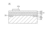
図4に示すように、第2の実施形態に係る発光ダイオード素子10は、素子構造体11を構成するn型半導体層12における活性層13の反対側(上側)の面上に、チタン(Ti)とアルミニウム(Al)との積層体からなり、ボンディングパッドを兼ねるn側電極17Aが選択的に形成されている。p型半導体層14における活性層13の反対側(下側)には、白金(Pt)と金(Au)との積層体からなり、活性層13からの発光光に対する反射率が90%以上となるように設けられたp側電極15Aが形成されている。また、p側電極15Aにおける外側のAu層を下地層として、厚さが約50μmの金めっきされた金属膜18が形成されている。
【0088】
第2の実施形態の特徴として、素子構造体11の周縁部におけるp型半導体層14とp側電極15Aとの間には、例えば酸化シリコン(SiO2 )からなる電流狭窄膜23を設けている。これにより、素子構造体11の側端面を通ってリークするリーク電流を低減できるため、発光素子の発光効率が向上する。
【0089】
このように、第2の実施形態によると、発光ダイオード素子10を構成する素子構造体11の下側に、活性層13からの発光光に対する反射率が90%以上となるように設けられた金属からなるp側電極15Aが形成されている。これにより、活性層13から出射される発光光はp側電極15Aにより反射され、n型半導体層12におけるn側電極17Aが設けられていない部分を通して取り出されるため、光の取り出し効率を大幅に向上することができる。
【0090】
その上、p側電極15Aにおける素子構造体11の反対側(下側)の面上には、単結晶からなる基板に代えて金属膜18を設けているため、活性層13で生じた熱は金属膜18を介して外部に放熱される。このように、GaN系半導体からなる素子構造体11を成長させる単結晶基板に代えて金属膜18を設けていることにより、放熱性が格段に向上するため、本実施形態に係る発光ダイオード素子10の高出力動作が可能となる。また、サファイアのような絶縁性基板を有さないため、静電耐圧性も向上する。
【0091】
なお、金属膜18と接するp側電極15Aは、白金(Pt)と金(Au)との積層構造に限られず、金(Au)、白金(Pt)、銅(Cu)、銀(Ag)及びロジウム(Rh)のうちの少なくとも1つからなる単層膜、又はこれらのうちの2つ以上を含む積層構造としても良い。
【0092】
以下、前記のように構成された発光ダイオード素子10の製造方法について図面を参照しながら説明する。
【0093】
図5(a)〜図5(c)乃至図7(a)〜図7(c)は本発明の第2の実施形態に係る発光ダイオード素子の製造方法の工程順の断面構成を示している。
【0094】
まず、図5(a)に示すように、第1の実施形態と同様に、MOCVD法により、ウエハ状のサファイアからなる基板20の主面上に、n型AlGaNからなるn型半導体層12、InGaNからなる活性層13及びp型AlGaNからなるp型半導体層14を順次成長することにより、n型半導体層12、活性層13及びp型半導体層14を含む素子構造体11を形成する。
【0095】
続いて、素子構造体11、すなわちp型半導体層14の上に、例えば気相堆積(CVD)法により、膜厚が約300nmの酸化シリコンからなる電流狭窄形成膜を堆積する。続いて、堆積した電流狭窄形成膜に対して例えばフッ化水素酸(HF)を用いたウエットエッチングを行なって、電流狭窄形成膜から素子構造体11の発光領域を露出する開口部を持つ複数の電流狭窄膜23を形成する。その後、電子ビーム蒸着法により、各電流狭窄膜23及びp型半導体層14における電流狭窄膜23からの露出領域を含む全面にわたって、厚さが約50nmのPt層と厚さが約200nmのAu層とからなるp側電極15Aを形成する。
【0096】
次に、図5(b)に示すように、金めっき法により、p側電極15Aの上に、該p側電極15AのAu層を下地層として厚さが約50μmの金属膜18を成膜する。
【0097】
次に、図5(c)に示すように、金属膜18の上に、可塑性に優れる膜状の保持部材、例えば厚さが約100μmの高分子フィルムからなる第1の保持膜42を接着する。ここで、第1の保持膜42には、その保持面に約120℃の加熱により発泡して接着力が低下する接着剤層を設けた、例えばポリエステルからなる高分子フィルムを用いる。続いて、基板20に対して素子構造体11の反対側の面から、パルス状に発振する波長が355nmであるYAGレーザの第3高調波光を基板20をスキャンするように照射する。前述したように、照射されたレーザ光は、基板20では吸収されず、素子構造体11、すなわちn型半導体層12で吸収される。このレーザ光の吸収により、n型半導体層12は局所的に発熱し、該n型半導体層12はその基板20との界面において原子同士の結合が切断されて、基板20とn型半導体層12との間に金属ガリウムを含む熱分解層(図示せず)が形成される。なお、照射するレーザ光の光源には、YAGレーザの第3高調波光に代えて、波長が248nmであるKrFエキシマレーザ光を用いてもよい。さらには、レーザ光源に代えて、波長が365nmである水銀ランプの輝線を用いてもよい。
【0098】
次に、図6(a)に示すように、塩酸等を用いたウエットエッチングによって熱分解層を溶融することにより、素子構造体11から基板20を分離して除去する。続いて、基板20を除去された素子構造体11におけるn型半導体層12の活性層13の反対側の面上に、例えば電子ビーム蒸着法により、膜厚が約50nmのTiと膜厚が約800nmのAlとの積層膜を蒸着し、蒸着した積層膜に対して、素子構造体11の発光領域を部分的に覆うようにパターニングを行なって、積層膜からボンディングパッドとしても機能するn側電極17Aを形成する。
【0099】
次に、図6(b)に示すように、n側電極17Aを含めn型半導体層12の上に、例えば厚さが約100μmの高分子フィルムからなる第2の保持膜43を接着する。第2の保持膜43には、その保持面に約170℃の加熱により発泡して接着力が低下する接着剤層を設けた、例えばポリエステルからなる高分子フィルムを用いる。
【0100】
次に、第1の保持膜42及び第2の保持膜43により保持された素子構造体11を約120℃に加熱する。この約120℃の加熱により、第1の保持膜42に設けられた接着剤層が発泡して金属膜18との間の接着力が低下するため、図6(c)に示すように、第1の保持膜42は金属膜18から容易に分離される。このとき、金属膜18の表面には第1の保持膜42の接着剤が残るおそれはない。
【0101】
次に、図7(a)に示すように、金属膜18における素子構造体11のチップ分割領域と対応する部分、すなわち電流狭窄膜23の上側部分を選択的にエッチングして、p側電極15Aにおけるチップ分割領域を露出する。第2の実施形態においても、基板20の分離工程、n側電極17Aの各成膜工程は素子構造体11に第1の保持膜42を設けた状態で行ない、金属膜18に対するエッチング工程は、素子構造体11に第2の保持膜43を設けた状態で行なうため、素子構造体11の膜厚が例えば5μm程度と極めて薄い構造であっても、何ら不具合を生じることなく実施することができる。
【0102】
次に、図7(b)に示すように、第2の保持膜43に保持されたp側電極15Aにおける金属膜18からの露出領域(ダイシング領域)及びその下方をダイシングブレード50を用いて切断する。これにより、各素子構造体11は、平面サイズが例えば300μm角の発光ダイオードチップを得る。このとき、第2の保持膜43に対してはその途中までを切断する。
【0103】
次に、図7(c)に示すように、第2の保持膜43を約170℃に加熱することにより、第2の保持膜43に設けられた接着剤層が発泡して各チップとの間の接着力が低下するため、第2の保持膜43から各チップが容易に剥離する。その後は、後工程であるダイスボンディング等の組み立て工程で実装される。
【0104】
以上説明したように、第2の実施形態に係る製造方法によると、高輝度で、放熱性及び静電耐圧に優れ且つ直列抵抗が小さい発光ダイオード素子10を得ることができる。
【0105】
(第2の実施形態の一変形例)
以下、本発明の第2の実施形態の一変形例について図面を参照しながら説明する。
【0106】
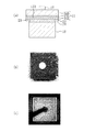
図8(a)〜図8(c)は本発明の第2の実施形態の一変形例に係る発光ダイオード素子であって、図8(a)は断面構成を示し、図8(b)はチップ表面の走査型電子顕微鏡(Scanning Electron Microscpe:SEM)による顕微鏡写真を示し、図8(c)は発光状態にあるチップ表面の写真を示している。また、図8(a)において、図4に示す構成部材と同一の構成部材には同一の符号を付すことにより説明を省略する。
【0107】
本変形例は試作例であって、図8(a)に示すように、素子構造体11のn型半導体層12Aにはn型GaNを用い、活性層13AにはInGaNからなる多重量子井戸構造を用い、p型半導体層14Aにはp型GaNを用いている。ここで、チップの平面サイズは300μm角である。
【0108】
n型半導体層12Aの上には、発光領域の中央部分にTi/Auの積層体からなるn側電極17が設けられている。p側電極15BにはPtを用い、該p側電極15Bの素子構造体11の反対側の面上には、Ti/Auからなるめっき下地層24を設けている。
【0109】
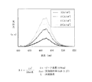
図9に本変形例に係る発光ダイオード素子10の発光スペクトルの測定結果を示す。図9のグラフに示すように、動作電流を増加させるにつれて、活性層13Aに対して垂直な方向に共振するいわゆる垂直共振器作用による複数のピークが現われる。
【0110】
(第3の実施形態)
以下、本発明の第3の実施形態について図面を参照しながら説明する。
【0111】
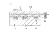
図10は本発明の第3の実施形態に係る半導体発光素子であって、青色又は緑色等の短波長発光が可能な発光ダイオード素子の断面構成を示している。図10において、図4に示す構成部材と同一の構成部材には同一の符号を付すことにより説明を省略する。
【0112】
第3の実施形態に係る発光ダイオード素子を構成する素子構造体11は、n型半導体層12における活性層13の反対側の面上に、例えばITOからなり透光性を有するn側電極17Bが設けられ、該n側電極17B上の一部の領域にはAuからなるボンディングパッド16が形成されている。
【0113】
ここで、活性層13は例えば量子井戸構造を有していても良い。活性層13において生成された例えば波長が470nmの青色発光光は、Pt/Auからなるp側電極15Aにより反射され、ITOからなるn側電極17Bを透過して外部に取り出される。
【0114】
このように、第3の実施形態によると、発光ダイオード素子10を構成する素子構造体11の下側に、活性層13からの発光光に対する反射率が90%以上となるように設けられた金属からなるp側電極15Aが形成されている。これにより、活性層13から出射される発光光はp側電極15Aにより反射され、n型半導体層12に設けられた透光性を持つn側電極17Bを通して取り出されるため、光の取り出し効率を大幅に向上することができる。
【0115】
その上、p側電極15Aにおける素子構造体11の反対側(下側)の面上には、単結晶からなる基板に代えて金属膜18を設けているため、活性層13で生じた熱は金属膜18を介して外部に放熱される。このように、GaN系半導体からなる素子構造体11を成長させる単結晶基板に代えて金属膜18を設けていることにより、放熱性が格段に向上するため、本実施形態に係る発光ダイオード素子10の高出力動作が可能となる。また、サファイアのような絶縁性基板を有さないため、静電耐圧性も向上する。
【0116】
以下、前記のように構成された発光ダイオード素子10の製造方法について図面を参照しながら説明する。
【0117】
図11(a)〜図11(c)乃至図13(a)〜図13(c)は本発明の第3の実施形態に係る発光ダイオード素子の製造方法の工程順の断面構成を示している。
【0118】
まず、図11(a)に示すように、MOCVD法により、ウエハ状のサファイアからなる基板20の主面上に、n型AlGaNからなるn型半導体層12、InGaNからなる活性層13及びp型AlGaNからなるp型半導体層14を順次成長することにより、n型半導体層12、活性層13及びp型半導体層14を含む素子構造体11を形成する。
【0119】
次に、図11(b)に示すように、素子構造体の11のp型半導体層14の上に、例えば厚さが約100μmの高分子フィルムからなる第1の保持膜42を接着する。ここで、第1の保持膜42には、その保持面に約120℃の加熱により発泡して接着力が低下する接着剤層を設けた、例えばポリエステルからなる高分子フィルムを用いる。続いて、基板20に対して素子構造体11の反対側の面から、パルス状に発振する波長が355nmであるYAGレーザの第3高調波光を基板20をスキャンするように照射する。前述したように、照射されたレーザ光は、基板20では吸収されず、素子構造体11、すなわちn型半導体層12で吸収される。このレーザ光の吸収により、n型半導体層12は局所的に発熱し、該n型半導体層12はその基板20との界面において原子同士の結合が切断されて、基板20とn型半導体層12との間に金属ガリウムを含む熱分解層(図示せず)が形成される。なお、照射するレーザ光の光源には、YAGレーザの第3高調波光に代えて、波長が248nmであるKrFエキシマレーザ光を用いてもよい。さらには、レーザ光源に代えて、波長が365nmである水銀ランプの輝線を用いてもよい。
【0120】
次に、図11(c)に示すように、塩酸等を用いたウエットエッチングによって熱分解層を溶融することにより、素子構造体11から基板20を分離して除去する。続いて、基板20を除去された素子構造体11におけるn型半導体層12の活性層13の反対側の面上に、例えばRFスパッタ法によりITO膜を堆積し、堆積したITO膜をパターニングしてn側電極17Bを形成する。さらに、形成したn側電極17Bの上に、例えば電子ビーム蒸着法により、Auからなる電極形成膜を蒸着し、蒸着した電極形成膜に対してn側電極17B上の一部分を覆うようにパターニングを行なって、電極形成膜からボンディングパッド16を形成する。なお、電極形成膜の膜厚は500nm以上とすることが好ましい。また、ITO膜と電極形成膜とのパターニングは同時に行なってもよい。
【0121】
次に、図12(a)に示すように、ボンディングパッド16及びn側電極17Bを含むn型半導体層12の上に、例えば厚さが約100μmの高分子フィルムからなる第2の保持膜43を接着する。第2の保持膜43には、その保持面に約170℃の加熱により発泡して接着力が低下する接着剤層を設けた、例えばポリエステルからなる高分子フィルムを用いる。
【0122】
次に、第1の保持膜42及び第2の保持膜43により保持された素子構造体11を約120℃に加熱する。この約120℃の加熱により、第1の保持膜42に設けられた接着剤層が発泡して素子構造体11のp型半導体層14との間の接着力が低下するため、図12(b)に示すように、第1の保持膜42はp型半導体層14から容易に分離される。このとき、p型半導体層14の表面には第1の保持膜42の接着剤が残るおそれはない。
【0123】
次に、図12(c)に示すように、電子ビーム蒸着法により、p型半導体層14の上に全面にわたって、厚さが約50nmのPt層と厚さが約200nmのAu層とからなるp側電極15Aを形成する。続いて、金めっき法により、p側電極15Aの上に、該p側電極15AのAu層を下地層として厚さが約50μmの金属膜18を成膜する。
【0124】
次に、図13(a)に示すように、金属膜18における素子構造体11のチップ分割領域と対応する部分を選択的にエッチングして、p側電極15Aにおけるチップ分割領域を露出する。第3の実施形態においても、基板20の分離工程、n側電極17B及びボンディングパッド16の各成膜工程は素子構造体11に第1の保持膜42を設けた状態で行ない、p側電極15A、金属膜18の各成膜工程及び金属膜18に対するエッチング工程は、素子構造体11に第2の保持膜43を設けた状態で行なうため、素子構造体11の膜厚が例えば5μm程度と極めて薄い構造であっても、何ら不具合を生じることなく実施することができる。
【0125】
次に、図13(b)に示すように、第2の保持膜43に保持されたp側電極15Aにおける金属膜18からの露出領域(ダイシング領域)及びその下方をダイシングブレード50を用いて切断する。これにより、各素子構造体11は、平面サイズが例えば300μm角の発光ダイオードチップを得る。このとき、第2の保持膜43に対してはその途中までを切断する。
【0126】
次に、図13(c)に示すように、第2の保持膜43を約170℃に加熱することにより、第2の保持膜43に設けられた接着剤層が発泡して各チップとの間の接着力が低下するため、第2の保持膜43から各チップが容易に剥離する。その後は、後工程であるダイスボンディング等の組み立て工程で実装される。
【0127】
以上説明したように、第3の実施形態に係る製造方法によると、高輝度で、放熱性及び静電耐圧に優れ且つ直列抵抗が小さい発光ダイオード素子10を得ることができる。
【0128】
(第4の実施形態)
以下、本発明の第4の実施形態について図面を参照しながら説明する。
【0129】
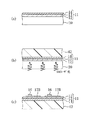
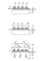
図14は本発明の第4の実施形態に係る半導体発光素子であって、青色又は緑色等の短波長発光が可能な発光ダイオード素子の断面構成を示している。図14において、図10に示す構成部材と同一の構成部材には同一の符号を付すことにより説明を省略する。
【0130】
図14に示すように、第4の実施形態は、素子構造体11におけるp型半導体層14とp側電極15Aとの間に、それぞれが、例えば酸化シリコン(SiO2 )からなる第1誘電体層と酸化シリコンよりも屈折率が大きい酸化タンタル(Ta2O5)からなる第2誘電体層とが交互に積層されてなる複数のミラー構造体25が互いに間隔をおいて形成されていることを特徴とする。
【0131】
各ミラー構造体25は、第1誘電体層の厚さを80nmとし、第2誘電体層の厚さを53nmとし、これら第1誘電体層及び第2誘電体層を1周期としてその10周期分が積層されている。ここで、各誘電体層の厚さは、発光波長を470nmとし、光学波長をλとしたときに、そのλ/4が反射率の最大となるように設計されている。
【0132】
ここで、活性層13は例えば量子井戸構造を有していても良い。活性層13において生成された例えば波長が470nmの青色発光光は、Pt/Auからなるp側電極15A及び各ミラー構造体25により反射され、ITOからなるn側電極17Bを透過して外部に取り出される。
【0133】
このように、第4の実施形態によると、発光ダイオード素子10を構成する素子構造体11の下側に、活性層13からの発光光に対する反射率が90%以上となるように設けられた金属からなるp側電極15Aと、該発光光に対する反射率が90%以上の高反射率を有する誘電体からなるミラー構造体25が形成されている。これにより、活性層13から出射される発光光はp側電極15A及びミラー構造体25により反射され、n型半導体層12に設けられた透光性を持つn側電極17Bを通して取り出されるため、光の取り出し効率を大幅に向上することができる。
【0134】
その上、p側電極15Aにおける素子構造体11の反対側(下側)の面上には、単結晶からなる基板に代えて金属膜18を設けているため、活性層13で生じた熱は金属膜18を介して外部に放熱される。このように、GaN系半導体からなる素子構造体11を成長させる単結晶基板に代えて金属膜18を設けていることにより、放熱性が格段に向上するため、本実施形態に係る発光ダイオード素子10の高出力動作が可能となる。また、サファイアのような絶縁性基板を有さないため、静電耐圧性も向上する。
【0135】
なお、第4の実施形態においては、ミラー構造体25に積層した誘電体膜を用いたが、これに限られず、例えばエピタキシャル成長したGaN系半導体からなる積層膜を用い、互いに隣接する膜同士のアルミニウム(Al)やインジウム(In)の組成を変えて、互いに屈折率差を生じさせることにより、活性層13からの発光光を高い反射率で反射する構成としても良い。
【0136】
以下、前記のように構成された発光ダイオード素子10の製造方法について図面を参照しながら説明する。
【0137】
図15(a)〜図15(c)乃至図17(a)〜図17(c)は本発明の第4の実施形態に係る発光ダイオード素子の製造方法の工程順の断面構成を示している。
【0138】
まず、図15(a)に示すように、MOCVD法により、ウエハ状のサファイアからなる基板20の主面上に、n型AlGaNからなるn型半導体層12、InGaNからなる活性層13及びp型AlGaNからなるp型半導体層14を順次成長することにより、n型半導体層12、活性層13及びp型半導体層14を含む素子構造体11を形成する。
【0139】
続いて、素子構造体11、すなわちp型半導体層14の上に、例えばRFスパッタ法により、厚さが80nmのSiO2 からなる第1誘電体層と厚さが53nmのTa2O5からなる第2誘電体層とを1周期とし、その10周期分からなる誘電体積層膜を堆積する。続いて、堆積した誘電体積層膜に対して例えばフッ化水素酸(HF)を用いたウエットエッチングを行なうことにより、誘電体積層膜から互いに間隔をおいた複数のミラー構造体25を形成する。その後、電子ビーム蒸着法により、各ミラー構造体25及びp型半導体層14におけるミラー構造体25からの露出領域を含む全面にわたって、厚さが約50nmのPt層と厚さが約200nmのAu層とからなるp側電極15Aを形成する。
【0140】
次に、図15(b)に示すように、金めっき法により、p側電極15Aの上に、該p側電極15AのAu層を下地層として厚さが約50μmの金属膜18を成膜する。
【0141】
次に、図15(c)に示すように、金属膜18の上に、例えば厚さが約100μmの高分子フィルムからなる第1の保持膜42を接着する。ここで、第1の保持膜42には、その保持面に約120℃の加熱により発泡して接着力が低下する接着剤層を設けた、例えばポリエステルからなる高分子フィルムを用いる。続いて、基板20に対して素子構造体11の反対側の面から、パルス状に発振する波長が355nmであるYAGレーザの第3高調波光を基板20をスキャンするように照射する。前述したように、照射されたレーザ光は、基板20では吸収されず、素子構造体11、すなわちn型半導体層12で吸収される。このレーザ光の吸収により、n型半導体層12は局所的に発熱し、該n型半導体層12はその基板20との界面において原子同士の結合が切断されて、基板20とn型半導体層12との間に金属ガリウムを含む熱分解層(図示せず)が形成される。なお、照射するレーザ光の光源には、YAGレーザの第3高調波光に代えて、波長が248nmであるKrFエキシマレーザ光を用いてもよい。さらには、レーザ光源に代えて、波長が365nmである水銀ランプの輝線を用いてもよい。
【0142】
次に、図16(a)に示すように、塩酸等を用いたウエットエッチングによって熱分解層を溶融することにより、素子構造体11から基板20を分離して除去する。続いて、基板20を除去された素子構造体11におけるn型半導体層12の活性層13の反対側の面上に、例えばRFスパッタ法によりITO膜を堆積し、堆積したITO膜をパターニングしてn側電極17Bを形成する。さらに、形成したn側電極17Bの上に、例えば電子ビーム蒸着法により、Auからなる電極形成膜を蒸着し、蒸着した電極形成膜に対してn側電極17B上の一部分を覆うようにパターニングを行なって、電極形成膜からボンディングパッド16を形成する。なお、電極形成膜の膜厚は500nm以上、例えば約800nmとすることにより、ボンディングパッド16にワイヤボンディングが確実に実施されるようにする。また、ITO膜と電極形成膜とのパターニングは同時に行なってもよい。
【0143】
次に、図16(b)に示すように、ボンディングパッド16及びn側電極17Bを含めn型半導体層12の上に、例えば厚さが約100μmの高分子フィルムからなる第2の保持膜43を接着する。第2の保持膜43には、その保持面に約170℃の加熱により発泡して接着力が低下する接着剤層を設けた、例えばポリエステルからなる高分子フィルムを用いる。
【0144】
次に、第1の保持膜42及び第2の保持膜43により保持された素子構造体11を約120℃に加熱する。この約120℃の加熱により、第1の保持膜42に設けられた接着剤層が発泡して金属膜18との間の接着力が低下するため、図16(c)に示すように、第1の保持膜42は金属層18から容易に分離される。このとき、金属層18の表面には第1の保持膜42の接着剤が残るおそれはない。
【0145】
次に、図17(a)に示すように、金属膜18における素子構造体11のチップ分割領域と対応する部分を選択的にエッチングして、p側電極15Aにおけるチップ分割領域を露出する。第4の実施形態においても、基板20の分離工程、n側電極17B及びボンディングパッド16の各成膜工程は素子構造体11に第1の保持膜42を設けた状態で行ない、p側電極15A、金属膜18の各成膜工程及び金属膜18に対するエッチング工程は、素子構造体11に第2の保持膜43を設けた状態で行なうため、素子構造体11の膜厚が例えば5μm程度と極めて薄い構造であっても、何ら不具合を生じることなく実施することができる。
【0146】
次に、図17(b)に示すように、第2の保持膜43に保持されたp側電極15Aにおける金属膜18からの露出領域(ダイシング領域)及びその下方をダイシングブレード50を用いて切断する。これにより、各素子構造体11は、平面サイズが例えば300μm角の発光ダイオードチップを得る。このとき、第2の保持膜43に対してはその途中までを切断する。
【0147】
次に、図17(c)に示すように、第2の保持膜43を約170℃に加熱することにより、第2の保持膜43に設けられた接着剤層が発泡して各チップとの間の接着力が低下するため、第2の保持膜43から各チップが容易に剥離する。その後は、後工程であるダイスボンディング等の組み立て工程で実装される。
【0148】
以上説明したように、第4の実施形態に係る製造方法によると、高輝度で、放熱性及び静電耐圧に優れ且つ直列抵抗が小さい発光ダイオード素子10を得ることができる。
【0149】
なお、ミラー構造体25は、酸化シリコン(SiO2 )と酸化タンタル(Ta2O5)との積層構造に限られず、第2誘電体層を構成する高屈折率材料である酸化タンタルに代えて、酸化チタン(TiO2 )、酸化ニオブ(Nb2O5)又は酸化ハフニウム(HfO2 )を用いてもよい。
【0150】
また、誘電体からなる積層膜に代えて、窒化アルミニウムガリウムインジウム(AlxGayIn1−x−y N)(但し、0≦x、y≦1、0≦x+y≦1である。)の組成を代えることにより高反射率を有するミラー構造を形成する場合には、図15(a)に示す素子構造体11の結晶成長に連続してエピタキシャル成長により成膜できるため、誘電体を成膜する成膜装置を用いる必要がなくなる。なお、成膜した半導体膜から複数のミラー構造体25を得るパターニング工程には、例えば塩素(Cl2 )ガスを用いた反応性イオンエッチング(Reactive Ion Etching:RIE)法を用いれば良い。
【0151】
なお、第1〜第4の実施形態において、基板20の主面の面方位は特に限定されず、例えばサファイアの場合には、典型的な(0001)面や、さらには典型的な面からわずかにずれた面方位(オフオリエンテーション)を持たせてもよい。
【0152】
また、基板20上に成長する素子構造体11の結晶成長法は、MOCVD法に限られず、例えば、分子線エピタキシャル成長(MBE)法又はハイドライド気相成長(HVPE)法でもよい。また、これらの3つの成長法を各半導体層に応じて適宜使い分けてもよい。
【0153】
また、GaN系半導体からなる素子構造体11は、照射光を吸収する層が素子構造体11に含まれていれば良く、必ずしも照射光を吸収する層が基板20と接している必要はない。また、照射光を吸収する半導体層の組成は、例えばAlGaN又はInGaN等の任意の組成を持つIII−V族窒化物半導体であればよい。
【0154】
また、基板20と素子構造体11との間に、InGaN又はZnOのように、GaNよりも禁制帯幅が小さい光吸収層を設けてもよい。このようにすると、照射光の吸収が光吸収層により促進されるため、低出力の照射光でも光吸収層が分解される。
【0155】
また、レーザ光等は、基板20を保持膜41等の接着力が低下しない程度に加熱しながら照射してもよい。このようにすると、基板20と素子構造体11との間の熱膨張係数の差によるストレスを緩和しながら素子構造体11の半導体層を熱分解できるため、素子構造体11に発生するクラックを防止することができる。
【0156】
さらには、光照射工程の前か後に、素子構造体11の上に基板20及び素子構造体11との扱いを容易とするように、高分子材料フィルムに代えて、例えばシリコン(Si)、ヒ化ガリウム(GaAs)、リン化インジウム(InP)、リン化ガリウム(GaP)等の半導体からなる保持基板、又は銅(Cu)等の金属からなる保持基板を貼り合わせ、さらには除去してもよい。
【0157】
また、第2〜第4の実施形態においても、第1の実施形態の一変形例と同様に、基板20と下地層との間に熱分解層を形成した後に、素子構造体11を再成長してもよい。
【0158】
また、第1、第3及び第4の実施形態においても、第2の実施形態と同様に、チップの周縁部に電流狭窄膜を設けても良い。
【0159】
【発明の効果】
本発明に係る半導体発光素子及びその製造方法によると、素子構造を含む半導体積層膜が成長した基板を除去し、代わりに、比較的に厚膜の金属膜を設けるため、基板が残された状態と比べて該基板による発光光の吸収を抑制できる。その結果、半導体積層膜における金属膜の反対側の面からより多くの発光光を取り出すことが可能となる。また、基板を除去して金属膜を設けるため、直列抵抗を低減できる上に、放熱性が大幅に改善され且つ静電耐圧が大きくなる。
【0160】
本発明に係る半導体発光素子の実装方法によると、半導体積層膜の膜厚が例えば数μm以下と極めて小さい場合でも、膜状の保持部材を半導体積層膜に貼った状態でダイスボンディングを行なえるため、極めて薄い半導体発光素子を実装することが可能となる。
【図面の簡単な説明】
【図1】本発明の第1の実施形態に係る半導体発光素子を示す構成断面図である。
【図2】(a)〜(d)は本発明の第1の実施形態に係る半導体発光素子の製造方法を示す工程順の構成断面図である。
【図3】(a)〜(d)は本発明の第1の実施形態に係る半導体発光素子の製造方法を示す工程順の構成断面図である。
【図4】本発明の第2の実施形態に係る半導体発光素子を示す構成断面図である。
【図5】(a)〜(c)は本発明の第2の実施形態に係る半導体発光素子の製造方法を示す工程順の構成断面図である。
【図6】(a)〜(c)は本発明の第2の実施形態に係る半導体発光素子の製造方法を示す工程順の構成断面図である。
【図7】(a)〜(c)は本発明の第2の実施形態に係る半導体発光素子の製造方法を示す工程順の構成断面図である。
【図8】(a)〜(c)は本発明の第2の実施形態の一変形例に係る半導体発光素子を示し、(a)は構成断面図であり、(b)はSEMによるチップ表面の顕微鏡写真であり、(c)は発光状態にあるチップ表面の写真である。
【図9】本発明の第2の実施形態の一変形例に係る半導体発光素子の発光スペクトルを示すグラフである。
【図10】本発明の第3の実施形態に係る半導体発光素子を示す構成断面図である。
【図11】(a)〜(c)は本発明の第3の実施形態に係る半導体発光素子の製造方法を示す工程順の構成断面図である。
【図12】(a)〜(c)は本発明の第3の実施形態に係る半導体発光素子の製造方法を示す工程順の構成断面図である。
【図13】(a)〜(c)は本発明の第3の実施形態に係る半導体発光素子の製造方法を示す工程順の構成断面図である。
【図14】本発明の第4の実施形態に係る半導体発光素子を示す構成断面図である。
【図15】(a)〜(c)は本発明の第4の実施形態に係る半導体発光素子の製造方法を示す工程順の構成断面図である。
【図16】(a)〜(c)は本発明の第4の実施形態に係る半導体発光素子の製造方法を示す工程順の構成断面図である。
【図17】(a)〜(c)は本発明の第4の実施形態に係る半導体発光素子の製造方法を示す工程順の構成断面図である。
【図18】第1の従来例に係る発光ダイオード素子を示す構成断面図である。
【図19】第2の従来例に係る発光ダイオード素子を示す構成断面図である。
【符号の説明】
10 発光ダイオード素子
11 素子構造体(半導体積層膜)
12 n型半導体層
12A n型半導体層
13 活性層
13A 活性層
14 p型半導体層
14A p型半導体層
15 p側電極(ITO)
15A p側電極(Pt/Au)
15B p側電極(Pt)
16 ボンディングパッド
17 n側電極(Ti/Au)
17A n側電極(Ti/Al)
17B n側電極(ITO)
18 金属膜
20 基板
21 半田材
22 パッケージ
23 電流狭窄膜
24 めっき下地層
25 ミラー構造体
41 保持膜
42 第1の保持膜
43 第3の保持膜
50 ダイシングブレード
51 コレット[0001]
TECHNICAL FIELD OF THE INVENTION
The present invention relates to a semiconductor light emitting device such as a short wavelength light emitting diode device, a method for manufacturing the same, and a method for mounting the same.
[0002]
[Prior art]
General formula is B z Al x Ga 1-xyz In y N 1-vw As v P w (Where x, y, z, v, w are 0 ≦ x ≦ 1, 0 ≦ y ≦ 1, 0 ≦ z ≦ 1, 0 ≦ x + y + z ≦ 1, 0 ≦ v ≦ 1, 0 ≦ w ≦ 1, A group III-V nitride semiconductor (generally represented by BAlGaInNAsP, hereinafter referred to as a GaN-based semiconductor) represented by 0 ≦ v + w ≦ 1 is, for example, gallium nitride (GaN) at room temperature. Since the forbidden band has a relatively wide forbidden band of 3.4 eV, the light emitting device such as a visible light emitting diode element or a short wavelength semiconductor laser element for outputting blue light or green light, or under a high temperature. A wide variety of applications are expected, such as transistors that can operate at high speeds and large power transistors that can operate at high speed. As the light emitting device, a light emitting diode element and a semiconductor laser element have been commercialized. Above all, light emitting diode elements have been put to practical use in various display devices that output blue light or green light, large display devices, and traffic signals. Research and development of white light-emitting diode elements, which emit light when a fluorescent material is excited, are being actively pursued to increase the luminance and improve the luminous efficiency in order to realize so-called semiconductor lighting, which replaces existing fluorescent and incandescent lamps. It is being advanced.
[0003]
Heretofore, GaN-based semiconductors have been difficult to grow by the crystal growth method, like other wide-gap semiconductors. Recently, however, metal-organic chemical vapor deposition (MOCVD) methods have been used mainly for metal organic chemical vapor deposition (MOCVD). Since the crystal growth technology has greatly advanced, the above-mentioned light emitting diode element has been put to practical use.
[0004]
By the way, it is not easy to manufacture a substrate made of gallium nitride (GaN) as a substrate for growing a crystal growth layer (epitaxial layer). Therefore, a substrate such as silicon (Si) or gallium arsenide (GaAs) is used. In general, heteroepitaxial growth using a material different from that of the epitaxial layer for the substrate is performed because the manufacturing process itself cannot be performed and the epitaxial layer on the substrate cannot be grown on the substrate made of the same material.
[0005]
A GaN-based semiconductor grown on sapphire as a substrate has been most widely used and has exhibited the best device characteristics. Sapphire has the same hexagonal crystal structure as a GaN-based semiconductor and is extremely thermally stable, and thus is suitable for crystal growth of a GaN-based semiconductor requiring a high temperature of 1000 ° C. or higher. Therefore, conventionally, for a GaN-based semiconductor layer grown on a substrate mainly composed of sapphire, an attempt has been made to increase the luminance of the light-emitting diode element and to improve the luminous efficiency. For example, in order to achieve high brightness, two points are to improve internal quantum efficiency by improving crystallinity of a GaN-based semiconductor and suppressing non-radiative recombination, and to improve light extraction efficiency. is important.
[0006]
As described above, as a result of the recent remarkable progress of crystal growth technology, the improvement of internal quantum efficiency is approaching its limit. Therefore, improvement of light extraction efficiency has recently become an important issue.
[0007]
Hereinafter, two conventional techniques for improving the light extraction efficiency will be described with reference to the drawings.
[0008]
(First conventional example)
As shown in FIG. 18, a light emitting diode element according to a first conventional example is configured such that an n-
[0009]
As described above, the light emitting diode element according to the first conventional example uses the transparent p-
[0010]
(Second conventional example)
As shown in FIG. 19, the light-emitting diode element according to the second conventional example is so-called flip-chip mounting in which the p-
[0011]
Further, since the Ag forming the
[0012]
[Patent Document 1]
JP-A-07-94782
[Patent Document 2]
JP-A-11-191641
[Patent Document 3]
JP 2001-274507 A
[Patent Document 4]
JP 2001-313422 A
[0013]
[Problems to be solved by the invention]
However, the light emitting diode elements according to the first conventional example and the second conventional example are both formed on a
[0014]
In addition, since sapphire is insulative and has a low electrostatic withstand voltage, there is a problem that mounting cost is increased, for example, it is necessary to provide a protection diode element for surge suppression as in the second conventional example.
[0015]
Further, since the
[0016]
In view of the above-mentioned conventional problems, the present invention provides a semiconductor light emitting device made of a compound semiconductor, particularly a GaN-based semiconductor, which has improved heat dissipation and an increased electrostatic withstand voltage, further improved luminous efficiency and improved series resistance. It is intended to reduce the amount.
[0017]
[Means for Solving the Problems]
In order to achieve the above object, the present invention provides a semiconductor light emitting device, in which a counter electrode facing each other is formed on a front surface and a back surface of a semiconductor laminated film made of a compound semiconductor including an active layer, and a comparative electrode is formed on one of the counter electrodes. A structure in which a thick metal film is provided is adopted. Further, a material having a high reflectance for light emitted from the active layer is selected as one electrode material in contact with the metal film of the counter electrode, and a translucent material is selected as the other electrode material or a planar material thereof is selected. Keep dimensions as small as possible.
[0018]
Specifically, the semiconductor light emitting device according to the present invention includes a semiconductor laminated film including at least two semiconductor layers having different conductivity types, a first electrode formed on one surface of the semiconductor laminated film, A second electrode formed on a surface facing the one surface of the semiconductor multilayer film and a second electrode formed to be in contact with the first electrode or the second electrode, and having a thickness greater than or equal to the thickness of the semiconductor multilayer film; A metal film having a thickness.
[0019]
According to the semiconductor light emitting device of the present invention, the substrate on which the semiconductor laminated film including at least two semiconductor layers having different conductivity types is grown is removed, and instead, a film thickness larger or equal to the film thickness of the semiconductor laminated film is removed. By providing the metal film having the structure, absorption of emitted light by the substrate when the substrate is left can be suppressed. As a result, more emitted light can be extracted from the surface of the semiconductor laminated film opposite to the metal film. In addition, since a relatively thick metal film is provided by removing the substrate, series resistance can be reduced, heat dissipation is significantly improved, and electrostatic withstand voltage is increased. In addition, when a highly reflective material is used for the electrode in contact with the metal film, the luminous efficiency can be increased.
[0020]
In the semiconductor light emitting device of the present invention, the semiconductor laminated film is preferably made of a group III-V compound semiconductor containing nitrogen as a group V element. In this case, since a group III-V compound semiconductor containing nitrogen as a group V element, that is, a group III-V nitride semiconductor, often uses a different substrate such as sapphire, the effect of removing the different substrate is extremely large. large.
[0021]
In the semiconductor light emitting device of the present invention, the thickness of the metal film is preferably 10 μm or more.
[0022]
In the semiconductor light emitting device of the present invention, the metal film is preferably made of gold, copper or silver. In this case, since gold, copper, and silver all have high thermal conductivity, heat dissipation is further improved, so that a higher output operation can be reliably performed.
[0023]
In the semiconductor light emitting device of the present invention, the metal film is preferably formed by plating. By doing so, the metal film can be formed in a short time and with good reproducibility, so that a semiconductor light emitting device capable of high-output operation can be realized at low cost.
[0024]
In the semiconductor light emitting device of the present invention, it is preferable that the metal film includes a metal layer having a melting point of 300 ° C. or less at a portion opposite to the semiconductor laminated film. With this configuration, when the semiconductor light emitting device is die-bonded to a package or a lead frame, the metal layer having a melting point of 300 ° C. or less functions as a solder material, so that it is not necessary to use a solder material. Die bonding of the light emitting element can be performed at low cost.
[0025]
In this case, the metal layer preferably contains tin.
[0026]
In the semiconductor light emitting device of the present invention, an electrode formed to be in contact with the metal film among the first electrode and the second electrode has a reflectance of 90% or more with respect to light emitted from the semiconductor laminated film. Preferably. In this case, since the light extraction efficiency is improved, high luminance of the light emitting element can be realized.
[0027]
In the semiconductor light emitting device of the present invention, the electrode formed so as to be in contact with the metal film among the first electrode and the second electrode is a single layer made of at least one of gold, platinum, copper, silver and rhodium. It is preferable to use a film or a laminated film including two or more of them. This makes it possible to reliably form an electrode having a reflectance of 90% or more with respect to light emitted from the semiconductor laminated film.
[0028]
The semiconductor light emitting device of the present invention further includes a mirror structure formed between the semiconductor laminated film and the metal film and made of a dielectric or a semiconductor, and the mirror structure is provided for light emitted from the semiconductor laminated film. Preferably, it has a reflectance of 90% or more. With this configuration, the mirror structure has a higher light extraction efficiency than an electrode made of a single material having a high reflectivity, so that a higher luminance of the light emitting element can be realized.
[0029]
In this case, the mirror structure is made of any one of silicon oxide, titanium oxide, niobium oxide, tantalum oxide, and hafnium oxide, or aluminum gallium indium nitride (Al x Ga y In 1-xy N) (where 0 ≦ x, y ≦ 1, 0 ≦ x + y ≦ 1), and is preferably formed such that the refractive index with respect to the wavelength of light emitted from the semiconductor laminated film changes periodically. . By doing so, the difference in the refractive index of each layer constituting the mirror structure increases, so that a mirror structure having a high reflectance can be obtained even if the number of layers is reduced.
[0030]
In the semiconductor light emitting device of the present invention, it is preferable that an electrode provided on the opposite side of the metal film with respect to the semiconductor laminated film among the first electrode and the second electrode has a light transmitting property. With this configuration, the emitted light emitted from the semiconductor laminated film is extracted through the translucent electrode, so that the light extraction efficiency is improved.
[0031]
Further, in the semiconductor light emitting device of the present invention, the electrode provided on the side opposite to the metal film with respect to the semiconductor laminated film among the first electrode and the second electrode is made of indium tin oxide or has a thickness of Is preferably made of a metal containing nickel of 20 nm or less. In this case, a light-transmitting electrode can be reliably formed.
[0032]
It is preferable that the semiconductor light emitting device of the present invention further includes a current confinement film formed of a dielectric and formed between the semiconductor laminated film and the metal film and on a side portion thereof.
[0033]
The method of manufacturing a semiconductor light emitting device according to the present invention includes the steps of: (a) forming a semiconductor laminated film including at least two semiconductor layers having different conductivity types on a substrate made of single crystal; (B) separating a first electrode on one surface of the semiconductor multilayer film and forming a second electrode on a surface facing the one surface of the semiconductor multilayer film (c). ) And a step (d) of forming a metal film on one of the first electrode and the second electrode.
[0034]
According to the method for manufacturing a semiconductor light emitting device of the present invention, a semiconductor laminated film including at least two semiconductor layers having different conductivity types is formed on a substrate, and subsequently, the substrate is separated from the semiconductor laminated film. A first electrode is formed on one surface of the semiconductor laminated film, a second electrode is formed on a surface facing the one surface of the semiconductor laminated film, and one of the first electrode and the second electrode is further formed. A metal film on the substrate. As described above, since the substrate on which the semiconductor laminated film is formed is separated from the semiconductor laminated film, absorption of emitted light by the substrate can be suppressed, so that more emitted light is emitted from the surface of the semiconductor laminated film opposite to the metal film. You will be able to take it out. In addition, since the metal film is provided on the semiconductor laminated film with an electrode interposed in place of the substrate, the series resistance in the semiconductor laminated film can be reduced, the heat dissipation can be significantly improved, and the electrostatic breakdown voltage increases. .
[0035]
In the method for manufacturing a semiconductor light emitting device of the present invention, the semiconductor laminated film is preferably made of a III-V compound semiconductor containing nitrogen as a group V element.
[0036]
In the method for manufacturing a semiconductor light emitting device of the present invention, in the step (b), irradiation light having a wavelength that transmits through the substrate and is absorbed by a part of the semiconductor laminated film is applied from a surface of the substrate opposite to the semiconductor laminated film. It is preferable that the substrate be separated from the semiconductor laminated film by irradiating to form a decomposition layer in which a part of the semiconductor laminated film is decomposed inside the semiconductor laminated film. In this case, even when the area of the substrate is relatively large, the substrate and the semiconductor multilayer film can be separated with good reproducibility.
[0037]
In the method for manufacturing a semiconductor light emitting device of the present invention, it is preferable that the substrate is separated from the semiconductor laminated film by removing the substrate by polishing in the step (b). In this case, even when the area of the substrate is relatively large, the semiconductor stacked film can be separated at low cost.
[0038]
In the method for manufacturing a semiconductor light emitting device of the present invention, in the step (a), after forming a part of the semiconductor laminated film, the semiconductor light is transmitted through the substrate and absorbed by the semiconductor laminated film from a surface of the substrate opposite to the semiconductor laminated film. Forming a decomposed layer formed by decomposing the semiconductor laminated film inside a part of the semiconductor laminated film by irradiating irradiation light having a predetermined wavelength; and forming one of the semiconductor laminated films after forming the decomposed layer. Forming a remaining portion of the semiconductor laminated film on the portion. With this configuration, the semiconductor laminated film and the substrate are loosely coupled to each other through the decomposition layer formed by decomposing a part of the semiconductor laminated film. Therefore, when the remaining portion of the semiconductor laminated film is formed on a part of the semiconductor laminated film after the formation of the decomposition layer, when the remaining portion of the semiconductor laminated film includes, for example, a device structure (active layer), the substrate and the semiconductor Since it is less likely to be affected by the difference in thermal expansion coefficient between the laminated film and the lattice mismatch, the crystallinity of the device structure is improved, and a high-luminance semiconductor light emitting device can be obtained.
[0039]
It is preferable that the irradiation light applied to the substrate be laser light which oscillates in a pulse shape. The irradiation light is preferably a bright line of a mercury lamp. In this case, when a pulsed laser beam is used as the light source, the output power of the light can be significantly increased, so that the semiconductor stacked film can be easily separated. In addition, when a bright line of a mercury lamp is used as a light source, although the output power of light is inferior to that of laser light, the spot size can be made larger than in the case of laser light, so that the throughput in the irradiation step is improved.
[0040]
It is preferable that the irradiation light is irradiated so as to scan the surface of the substrate. With this configuration, even if the substrate has a relatively large area, the substrate can be separated from the semiconductor multilayer film without being affected by the beam size of the light source.
[0041]
Further, it is preferable that the irradiation light is irradiated while heating the substrate. By doing so, the difference in the thermal expansion coefficient between the semiconductor laminated film and the substrate that occurs during cooling after crystal growth and the stress that occurs in the semiconductor laminated film due to lattice mismatch between the two are alleviated. Cracks that occur in the semiconductor laminated film can be prevented.
[0042]
In the method for manufacturing a semiconductor light emitting device of the present invention, a laminated film made of a dielectric or a semiconductor is formed on a semiconductor laminated film between steps (a) and (b), and the formed laminated film is patterned. Further comprising the step of: (e) forming one of the first electrode and the second electrode on the patterned laminated film in the step (c); The film is preferably formed on an electrode formed on the patterned laminated film. This makes it possible to form a mirror structure that reflects light emitted from the semiconductor laminated film with high efficiency. In addition, in order to pattern a mirror structure composed of a laminated film made of a dielectric or a semiconductor, which is generally difficult to lower the resistance, an electrode and a metal film are formed in gaps between the patterned mirror structures. Thus, a sufficient operating current can be reliably injected from the gap.
[0043]
In this case, in the step (c), after separating the substrate from the semiconductor laminated film, the other of the first electrode and the second electrode is formed on a surface of the semiconductor laminated film opposite to the laminated film. Is preferred.
[0044]
In the method for manufacturing a semiconductor light emitting device according to the present invention, a first film-shaped film holding the semiconductor laminated film is formed between the step (a) and the step (b), the material being different from the material constituting the semiconductor laminated film. It is preferable that the method further includes a step (f) of attaching the holding member to the semiconductor multilayer film, and a step (g) of peeling the first holding member from the semiconductor multilayer film after the step (b). With this configuration, cracks generated in the semiconductor multilayer film in the process of relieving stress in the film when forming the decomposition layer in a part of the semiconductor multilayer film can be suppressed. As a result, even when the area of the substrate is relatively large, the substrate can be separated without generating cracks in the semiconductor stacked film.
[0045]
In this case, in the method for manufacturing a semiconductor light emitting device of the present invention, before the step (g), the film-like second holding member having a characteristic different from that of the first holding member is replaced with the first holding member in the semiconductor laminated film. It is preferable that the method further includes a step (h) of attaching the second holding member to the surface opposite to the holding member, and a step (i) of peeling the second holding member from the semiconductor multilayer film after the step (g). . This makes it possible to form an electrode on an arbitrary surface of the semiconductor multilayer film and pattern the metal film even after the substrate is separated from the semiconductor multilayer film.
[0046]
In this case, the first holding member or the second holding member is preferably a polymer material film, a single crystal substrate made of a semiconductor, or a metal plate. In this case, the polymer film or the metal plate is excellent in plasticity, and the single crystal substrate made of a semiconductor is excellent in cleavage, so that the substrate can be more easily separated.
[0047]
In this case, the polymer material film is preferably provided with an adhesive layer which can be peeled off by heating on the bonding surface. This eliminates the problem that the adhesive layer remains on the semiconductor laminated film when the polymer material film is peeled off, so that the polymer material film can be easily and reliably peeled from the semiconductor laminated film. Become so.
[0048]
The method for manufacturing a semiconductor light emitting device of the present invention may further include, before the step (c), a step (j) of selectively forming a current confinement film made of a dielectric on the semiconductor laminated film. preferable.
[0049]
The method for mounting a semiconductor light emitting device according to the present invention comprises the steps of: (a) forming a semiconductor laminated film including at least two semiconductor layers having different conductivity types on a single crystal substrate; (B) attaching a film-shaped holding member made of a material different from the material to be formed and holding the semiconductor laminated film to the semiconductor laminated film, and dicing the semiconductor laminated film together with the holding member to separate each side. A step (c) of producing a plurality of chips held by the holding member, and a step (d) of performing die bonding on each chip held by the holding member and then separating the holding member from each chip. And
[0050]
According to the method for mounting a semiconductor light emitting element of the present invention, even when the thickness of the semiconductor laminated film is extremely small, for example, several μm or less, the die bonding can be performed in a state where the film-shaped holding member is adhered to the semiconductor laminated film. An extremely thin semiconductor light emitting element can be mounted.
[0051]
In the method for mounting a semiconductor light emitting device of the present invention, the holding member is preferably a polymer material film.
[0052]
In the method for mounting a semiconductor light-emitting element of the present invention, it is preferable that the polymer material film is provided with an adhesive layer which can be peeled off by heating on its bonding surface.
[0053]
BEST MODE FOR CARRYING OUT THE INVENTION
(1st Embodiment)
A first embodiment of the present invention will be described with reference to the drawings.
[0054]
FIG. 1 shows a cross-sectional structure of a semiconductor light emitting device according to a first embodiment of the present invention, which is a light emitting diode device capable of emitting short wavelength light such as blue or green light.
[0055]
As shown in FIG. 1, the light emitting
[0056]
On the
[0057]
The
[0058]
As a feature of the first embodiment, a
[0059]
As described above, according to the first embodiment, the n-
[0060]
In addition, the
[0061]
The thickness of the
[0062]
Further, the n-
[0063]
Further, the light-transmitting p-
[0064]
Hereinafter, a method for manufacturing the light emitting
[0065]
FIGS. 2A to 2D and FIGS. 3A to 3D show cross-sectional configurations in the order of steps of a method for manufacturing a light-emitting diode element according to the first embodiment of the present invention. .
[0066]
First, as shown in FIG. 2A, a wafer-like sapphire (single crystal Al) is formed, for example, by a metal organic chemical vapor deposition (MOCVD) method. 2 O 3 ), The n-
[0067]
Here, as shown in [Table 1], in the
[0068]
[Table 1]
As shown in Table 1, as is well known, the buffer layer made of GaN formed on the
[0070]
Subsequently, an ITO film is deposited on the
[0071]
Next, as shown in FIG. 2B, a film-like holding member having excellent plasticity, for example, a polymer film having a thickness of about 100 μm is formed on the
[0072]
Next, as shown in FIG. 2C, the
[0073]
Subsequently, an n-
[0074]
Next, as shown in FIG. 2D, portions of the
[0075]
Next, as shown in FIG. 3A, a region (dicing region) exposed from the
[0076]
Next, as shown in FIG. 3C, the upper surface of the holding
[0077]
Next, as shown in FIG. 3D, the chip is heated to, for example, about 200 ° C. during bonding. Thereby, the adhesive which is heated and foamed is applied to the holding
[0078]
As described above, in the first embodiment, since the die bonding is performed in a state where the holding
[0079]
If an alloy made of, for example, gold (Au) and tin (Sn) having a melting point of about 280 ° C. is formed on at least a lower portion of the
[0080]
As described above, according to the manufacturing method according to the first embodiment, it is possible to obtain the light emitting
[0081]
(Modification of manufacturing method)
In the first embodiment, after the
[0082]
Specifically, after a base layer made of a GaN-based semiconductor is grown on the
[0083]
In this way, the
[0084]
In order to separate and remove the
[0085]
(Second embodiment)
Hereinafter, a second embodiment of the present invention will be described with reference to the drawings.
[0086]
FIG. 4 shows a cross-sectional configuration of a semiconductor light emitting device according to a second embodiment of the present invention, which is capable of emitting light of a short wavelength such as blue or green. In FIG. 4, the same components as those shown in FIG.
[0087]
As shown in FIG. 4, the light emitting
[0088]
As a feature of the second embodiment, for example, silicon oxide (SiO 2) is provided between the p-
[0089]
As described above, according to the second embodiment, the metal provided below the
[0090]
In addition, since the
[0091]
Note that the p-
[0092]
Hereinafter, a method for manufacturing the light emitting
[0093]
5 (a) to 5 (c) to 7 (a) to 7 (c) show cross-sectional configurations in the order of steps of a method for manufacturing a light emitting diode element according to the second embodiment of the present invention. .
[0094]
First, as shown in FIG. 5A, similarly to the first embodiment, an n-
[0095]
Subsequently, a current constriction forming film made of silicon oxide having a thickness of about 300 nm is deposited on the
[0096]
Next, as shown in FIG. 5B, a
[0097]
Next, as shown in FIG. 5C, a film-like holding member having excellent plasticity, for example, a
[0098]
Next, as shown in FIG. 6A, the
[0099]
Next, as shown in FIG. 6B, a
[0100]
Next, the
[0101]
Next, as shown in FIG. 7A, a portion of the
[0102]
Next, as shown in FIG. 7B, the exposed region (dicing region) of the p-
[0103]
Next, as shown in FIG. 7 (c), by heating the
[0104]
As described above, according to the manufacturing method according to the second embodiment, it is possible to obtain the light-emitting
[0105]
(Modification of Second Embodiment)
Hereinafter, a modified example of the second embodiment of the present invention will be described with reference to the drawings.
[0106]
8A to 8C show a light-emitting diode element according to a modification of the second embodiment of the present invention. FIG. 8A shows a cross-sectional configuration, and FIG. FIG. 8C shows a micrograph of the chip surface by a scanning electron microscope (SEM), and FIG. 8C shows a photograph of the chip surface in a light emitting state. In FIG. 8A, the same components as those shown in FIG. 4 are denoted by the same reference numerals, and description thereof will be omitted.
[0107]
This modification is a prototype example, and as shown in FIG. 8A, a multiple quantum well structure in which n-type GaN is used for the n-type semiconductor layer 12A of the
[0108]
On the n-type semiconductor layer 12A, an n-
[0109]
FIG. 9 shows a measurement result of an emission spectrum of the light emitting
[0110]
(Third embodiment)
Hereinafter, a third embodiment of the present invention will be described with reference to the drawings.
[0111]
FIG. 10 shows a cross-sectional configuration of a semiconductor light emitting device according to a third embodiment of the present invention, which is a light emitting diode device capable of emitting light of a short wavelength such as blue or green. In FIG. 10, the same components as those shown in FIG. 4 are denoted by the same reference numerals, and description thereof will be omitted.
[0112]
In the
[0113]
Here, the
[0114]
As described above, according to the third embodiment, the metal provided below the
[0115]
In addition, since the
[0116]
Hereinafter, a method for manufacturing the light emitting
[0117]
11 (a) to 11 (c) to 13 (a) to 13 (c) show cross-sectional configurations in the order of steps of a method for manufacturing a light emitting diode element according to the third embodiment of the present invention. .
[0118]
First, as shown in FIG. 11A, an n-
[0119]
Next, as shown in FIG. 11B, a
[0120]
Next, as shown in FIG. 11C, the
[0121]
Next, as shown in FIG. 12A, a
[0122]
Next, the
[0123]
Next, as shown in FIG. 12C, a Pt layer having a thickness of about 50 nm and an Au layer having a thickness of about 200 nm are formed on the entire surface of the p-
[0124]
Next, as shown in FIG. 13A, a portion of the
[0125]
Next, as shown in FIG. 13B, the exposed region (dicing region) of the p-
[0126]
Next, as shown in FIG. 13 (c), by heating the
[0127]
As described above, according to the manufacturing method according to the third embodiment, it is possible to obtain the light emitting
[0128]
(Fourth embodiment)
Hereinafter, a fourth embodiment of the present invention will be described with reference to the drawings.
[0129]
FIG. 14 shows a cross-sectional structure of a semiconductor light-emitting device according to a fourth embodiment of the present invention, which is a light-emitting diode device capable of emitting light of a short wavelength such as blue or green. 14, the same components as those shown in FIG. 10 are denoted by the same reference numerals, and description thereof will be omitted.
[0130]
As shown in FIG. 14, in the fourth embodiment, between the p-
[0131]
Each
[0132]
Here, the
[0133]
As described above, according to the fourth embodiment, the metal provided below the
[0134]
In addition, since the
[0135]
In the fourth embodiment, the dielectric film laminated on the
[0136]
Hereinafter, a method for manufacturing the light emitting
[0137]
FIGS. 15 (a) to 15 (c) to 17 (a) to 17 (c) show cross-sectional configurations in the order of steps of a method for manufacturing a light emitting diode element according to the fourth embodiment of the present invention. .
[0138]
First, as shown in FIG. 15A, an n-
[0139]
Subsequently, on the
[0140]
Next, as shown in FIG. 15B, a
[0141]
Next, as shown in FIG. 15C, a
[0142]
Next, as shown in FIG. 16A, the
[0143]
Next, as shown in FIG. 16B, a
[0144]
Next, the
[0145]
Next, as shown in FIG. 17A, a portion of the
[0146]
Next, as shown in FIG. 17B, the exposed region (dicing region) of the p-
[0147]
Next, as shown in FIG. 17C, by heating the
[0148]
As described above, according to the manufacturing method according to the fourth embodiment, it is possible to obtain the light-emitting
[0149]
The
[0150]
Further, instead of the laminated film made of a dielectric, aluminum gallium indium nitride (Al x Ga y In 1-xy N) (where 0 ≦ x, y ≦ 1, 0 ≦ x + y ≦ 1) is used to form a mirror structure having a high reflectance by changing the composition, the element shown in FIG. Since the film can be formed by epitaxial growth following the crystal growth of the
[0151]
In the first to fourth embodiments, the plane orientation of the main surface of the
[0152]
The crystal growth method of the
[0153]
The
[0154]
Further, between the
[0155]
Further, the laser beam or the like may be irradiated while heating the
[0156]
Further, before or after the light irradiation step, instead of the polymer material film, for example, silicon (Si) or silicon (Si) may be used on the
[0157]
Also in the second to fourth embodiments, similarly to the modification of the first embodiment, after forming a thermal decomposition layer between the
[0158]
Also, in the first, third and fourth embodiments, similarly to the second embodiment, a current confinement film may be provided on the periphery of the chip.
[0159]
【The invention's effect】
According to the semiconductor light emitting device and the method of manufacturing the same according to the present invention, the substrate on which the semiconductor laminated film including the element structure has been grown is removed, and instead, a relatively thick metal film is provided. The absorption of emitted light by the substrate can be suppressed as compared with the case. As a result, more emitted light can be extracted from the surface of the semiconductor laminated film opposite to the metal film. Further, since the metal film is provided by removing the substrate, the series resistance can be reduced, and the heat dissipation is greatly improved and the electrostatic withstand voltage is increased.
[0160]
According to the method for mounting a semiconductor light emitting device according to the present invention, even when the thickness of the semiconductor laminated film is extremely small, for example, several μm or less, the die bonding can be performed with the film-shaped holding member adhered to the semiconductor laminated film. It is possible to mount an extremely thin semiconductor light emitting element.
[Brief description of the drawings]
FIG. 1 is a configuration sectional view showing a semiconductor light emitting device according to a first embodiment of the present invention.
FIGS. 2A to 2D are cross-sectional views illustrating a method of manufacturing the semiconductor light emitting device according to the first embodiment of the present invention in the order of steps.
FIGS. 3A to 3D are cross-sectional views illustrating a method of manufacturing the semiconductor light emitting device according to the first embodiment of the present invention in a process order.
FIG. 4 is a sectional view showing a configuration of a semiconductor light emitting device according to a second embodiment of the present invention.
FIGS. 5A to 5C are cross-sectional views in the order of steps showing a method for manufacturing a semiconductor light emitting device according to a second embodiment of the present invention.
FIGS. 6A to 6C are cross-sectional views in the order of steps showing a method for manufacturing a semiconductor light emitting device according to a second embodiment of the present invention.
FIGS. 7A to 7C are sectional views in the order of steps showing a method for manufacturing a semiconductor light emitting device according to a second embodiment of the present invention.
8 (a) to 8 (c) show a semiconductor light emitting device according to a modification of the second embodiment of the present invention, FIG. 8 (a) is a configuration sectional view, and FIG. 8 (b) is a chip surface by SEM (C) is a photograph of the surface of the chip in a light emitting state.
FIG. 9 is a graph showing an emission spectrum of a semiconductor light emitting device according to a modification of the second embodiment of the present invention.
FIG. 10 is a sectional view showing a configuration of a semiconductor light emitting device according to a third embodiment of the present invention.
FIGS. 11A to 11C are cross-sectional views illustrating a method of manufacturing a semiconductor light emitting device according to a third embodiment of the present invention in the order of steps.
FIGS. 12A to 12C are cross-sectional views illustrating a method of manufacturing a semiconductor light emitting device according to a third embodiment of the present invention in the order of steps.
FIGS. 13A to 13C are cross-sectional views in the order of steps showing a method for manufacturing a semiconductor light emitting device according to a third embodiment of the present invention.
FIG. 14 is a configuration sectional view showing a semiconductor light emitting device according to a fourth embodiment of the present invention.
FIGS. 15A to 15C are cross-sectional views illustrating a method of manufacturing a semiconductor light emitting device according to a fourth embodiment of the present invention in the order of steps.
FIGS. 16A to 16C are cross-sectional views illustrating a method of manufacturing a semiconductor light emitting device according to a fourth embodiment of the present invention in the order of steps.
FIGS. 17A to 17C are cross-sectional views illustrating a method of manufacturing a semiconductor light emitting device according to a fourth embodiment of the present invention in the order of steps.
FIG. 18 is a configuration sectional view showing a light emitting diode element according to a first conventional example.
FIG. 19 is a configuration sectional view showing a light emitting diode element according to a second conventional example.
[Explanation of symbols]
10. Light emitting diode element
11 Element structure (semiconductor laminated film)
12 n-type semiconductor layer
12A n-type semiconductor layer
13 Active layer
13A Active layer
14 p-type semiconductor layer
14A p-type semiconductor layer
15 p-side electrode (ITO)
15A p-side electrode (Pt / Au)
15B p-side electrode (Pt)
16 Bonding pad
17 n-side electrode (Ti / Au)
17A n-side electrode (Ti / Al)
17B n-side electrode (ITO)
18 Metal film
20 substrates
21 Solder material
22 packages
23 Current constriction film
24 Plating underlayer
25 Mirror structure
41 Retention film
42 First Retaining Film
43 Third holding film
50 dicing blade
51 collet
Claims (33)
前記半導体積層膜の一方の面上に形成された第1の電極と、
前記半導体積層膜の前記一方の面と対向する対向面上に形成された第2の電極と、
前記第1の電極又は前記第2の電極と接するように形成され、前記半導体積層膜の膜厚よりも大きいか等しい膜厚を有する金属膜とを備えていることを特徴とする半導体発光素子。A semiconductor laminated film including at least two semiconductor layers having different conductivity types from each other;
A first electrode formed on one surface of the semiconductor laminated film;
A second electrode formed on a surface facing the one surface of the semiconductor laminated film;
A semiconductor film formed so as to be in contact with the first electrode or the second electrode and having a thickness greater than or equal to the thickness of the semiconductor laminated film.
前記ミラー構造体は、前記半導体積層膜から発光される光に対して90%以上の反射率を有していることを特徴とする請求項1、2又は8のいずれか1項に記載の半導体発光素子。Further comprising a mirror structure formed between the semiconductor laminated film and the metal film and made of a dielectric or a semiconductor,
9. The semiconductor according to claim 1, wherein the mirror structure has a reflectance of 90% or more with respect to light emitted from the semiconductor multilayer film. 10. Light emitting element.
前記基板を前記半導体積層膜から分離する工程(b)と、
前記半導体積層膜の一方の面上に第1の電極を形成し、前記半導体積層膜の前記一方の面と対向する対向面上に第2の電極を形成する工程(c)と、
前記第1の電極及び第2の電極のうちの一方の上に金属膜を形成する工程(d)とを備えていることを特徴とする半導体発光素子の製造方法。(A) forming a semiconductor laminated film including at least two semiconductor layers having different conductivity types on a single crystal substrate;
(B) separating the substrate from the semiconductor multilayer film;
(C) forming a first electrode on one surface of the semiconductor laminated film and forming a second electrode on a surface facing the one surface of the semiconductor laminated film;
Forming a metal film on one of the first electrode and the second electrode (d).
前記基板における前記半導体積層膜の反対側の面から、前記基板を透過し且つ前記半導体積層膜の一部に吸収される波長を有する照射光を照射して、前記半導体積層膜の内部に前記半導体積層膜の一部が分解してなる分解層を形成することにより、前記基板を前記半導体積層膜から分離することを特徴とする請求項15又は16に記載の半導体発光素子の製造方法。In the step (b),
By irradiating the substrate with irradiation light having a wavelength that passes through the substrate and is absorbed by a part of the semiconductor laminated film from a surface of the substrate opposite to the semiconductor laminated film, the semiconductor is formed inside the semiconductor laminated film. 17. The method according to claim 15, wherein the substrate is separated from the semiconductor laminated film by forming a decomposition layer in which a part of the laminated film is decomposed.
前記基板を研磨により除去することにより、前記基板を前記半導体積層膜から分離することを特徴とする請求項15又は16に記載の半導体発光素子の製造方法。In the step (b),
The method according to claim 15, wherein the substrate is separated from the semiconductor stacked film by removing the substrate by polishing.
前記半導体積層膜の一部を形成した後、前記基板における前記半導体積層膜の反対側の面から、前記基板を透過し且つ前記半導体積層膜に吸収される波長を有する照射光を照射することにより、前記半導体積層膜の一部の内部に前記半導体積層膜が分解してなる分解層を形成する工程と、
前記分解層を形成した後、前記半導体積層膜の一部の上に、前記半導体積層膜の残部を形成する工程とを含むことを特徴とする請求項15又は16に記載の半導体発光素子の製造方法。The step (a) comprises:
After forming a part of the semiconductor laminated film, by irradiating the substrate with irradiation light having a wavelength that transmits through the substrate and is absorbed by the semiconductor laminated film from a surface of the substrate opposite to the semiconductor laminated film. Forming a decomposition layer formed by decomposing the semiconductor laminated film inside a part of the semiconductor laminated film;
17. The method according to claim 15, further comprising, after forming the decomposition layer, forming a remaining portion of the semiconductor laminated film on a part of the semiconductor laminated film. Method.
前記半導体積層膜の上に誘電体又は半導体からなる積層膜を形成した後、形成した積層膜をパターニングする工程(e)をさらに備え、
前記工程(c)において、前記第1の電極及び第2の電極のうちのいずれか一方を、パターニングされた前記積層膜の上に形成し、
前記工程(d)において、前記金属膜は、パターニングされた前記積層膜の上に形成した電極の上に形成することを特徴とする請求項15又は16に記載の半導体発光素子の製造方法。Between the step (a) and the step (b),
After forming a laminated film made of a dielectric or a semiconductor on the semiconductor laminated film, the method further comprises a step (e) of patterning the formed laminated film,
In the step (c), one of the first electrode and the second electrode is formed on the patterned laminated film,
17. The method according to claim 15, wherein in the step (d), the metal film is formed on an electrode formed on the patterned laminated film.
前記半導体積層膜を構成する材料と異なる材料からなり、前記半導体積層膜を保持する膜状の第1の保持部材を前記半導体積層膜に貼り合わせる工程(f)と、
前記工程(b)よりも後に、前記第1の保持部材を前記半導体積層膜から剥離する工程(g)とをさらに備えていることを特徴とする請求項15又は16に記載の半導体発光素子の製造方法。Between the step (a) and the step (b),
(F) attaching a film-shaped first holding member made of a material different from the material constituting the semiconductor laminated film and retaining the semiconductor laminated film to the semiconductor laminated film;
17. The semiconductor light emitting device according to claim 15, further comprising, after the step (b), a step (g) of peeling the first holding member from the semiconductor laminated film. Production method.
前記工程(g)よりも後に、前記第2の保持部材を前記半導体積層膜から剥離する工程(i)とをさらに備えていることを特徴とする請求項26に記載の半導体発光素子の製造方法。Before the step (g), a film-shaped second holding member having a characteristic different from that of the first holding member is attached to a surface of the semiconductor laminated film opposite to the first holding member. Step (h),
27. The method according to claim 26, further comprising a step (i) of peeling the second holding member from the semiconductor multilayer film after the step (g). .
前記半導体積層膜を構成する材料と異なる材料からなり、前記半導体積層膜を保持する膜状の保持部材を前記半導体積層膜に貼り合わせる工程(b)と、
前記半導体積層膜を前記保持部材と共にダイシングを行なって、それぞれ個辺化された前記保持部材に保持された状態の複数のチップを作製する工程(c)と、
前記保持部材に保持された前記各チップに対してダイスボンディングを行なった後、前記保持部材を前記各チップから剥離する工程(d)とを備えていることを特徴とする半導体発光素子の実装方法。(A) forming a semiconductor laminated film including at least two semiconductor layers having different conductivity types on a single crystal substrate;
A step (b) of bonding a film-shaped holding member made of a material different from the material constituting the semiconductor laminated film and retaining the semiconductor laminated film to the semiconductor laminated film;
(C) dicing the semiconductor laminated film together with the holding member to produce a plurality of chips held by the individualized holding members;
(D) removing the holding member from each of the chips after performing die bonding on each of the chips held by the holding member. .
Priority Applications (1)
| Application Number | Priority Date | Filing Date | Title |
|---|---|---|---|
| JP2003175716A JP2004088083A (en) | 2002-06-25 | 2003-06-20 | Semiconductor light emitting device, its manufacturing method, and its packaging method |
Applications Claiming Priority (2)
| Application Number | Priority Date | Filing Date | Title |
|---|---|---|---|
| JP2002183919 | 2002-06-25 | ||
| JP2003175716A JP2004088083A (en) | 2002-06-25 | 2003-06-20 | Semiconductor light emitting device, its manufacturing method, and its packaging method |
Publications (2)
| Publication Number | Publication Date |
|---|---|
| JP2004088083A true JP2004088083A (en) | 2004-03-18 |
| JP2004088083A5 JP2004088083A5 (en) | 2009-03-12 |
Family
ID=32071589
Family Applications (1)
| Application Number | Title | Priority Date | Filing Date |
|---|---|---|---|
| JP2003175716A Pending JP2004088083A (en) | 2002-06-25 | 2003-06-20 | Semiconductor light emitting device, its manufacturing method, and its packaging method |
Country Status (1)
| Country | Link |
|---|---|
| JP (1) | JP2004088083A (en) |
Cited By (23)
| Publication number | Priority date | Publication date | Assignee | Title |
|---|---|---|---|---|
| JP2005340849A (en) * | 2004-05-26 | 2005-12-08 | Lumileds Lighting Us Llc | Led chip with built-in rapid switching diode for esd protection |
| JP2007013093A (en) * | 2005-07-01 | 2007-01-18 | Epitech Technology Corp | Light emitting diode |
| JP2007150314A (en) * | 2005-11-24 | 2007-06-14 | Samsung Electro Mech Co Ltd | Gallium-nitride-based light emitting diode with vertical-structure |
| US7244628B2 (en) | 2003-05-22 | 2007-07-17 | Matsushita Electric Industrial Co., Ltd. | Method for fabricating semiconductor devices |
| JP2007243047A (en) * | 2006-03-10 | 2007-09-20 | Matsushita Electric Works Ltd | Method for manufacturing light emitting device |
| JP2007258277A (en) * | 2006-03-20 | 2007-10-04 | Matsushita Electric Works Ltd | Semiconductor light emitting device |
| JP2008060279A (en) * | 2006-08-30 | 2008-03-13 | Mitsubishi Cable Ind Ltd | Nitride semiconductor light-emitting diode element and its manufacturing method |
| JP2008543032A (en) * | 2005-05-27 | 2008-11-27 | ラティス パワー (チアンシ) コーポレイション | InGaAlN light emitting device and manufacturing method thereof |
| JP2009534857A (en) * | 2006-04-27 | 2009-09-24 | オスラム オプト セミコンダクターズ ゲゼルシャフト ミット ベシュレンクテル ハフツング | Optoelectronic semiconductor chip |
| JP2010074122A (en) * | 2008-08-21 | 2010-04-02 | Sumitomo Electric Ind Ltd | Heat sink for led, heat sink precursor for led, led element, method for manufacturing heat sink for led and method for manufacturing led element |
| WO2010041370A1 (en) * | 2008-10-06 | 2010-04-15 | パナソニック株式会社 | Nitride semiconductor light emitting diode |
| US7763477B2 (en) | 2004-03-15 | 2010-07-27 | Tinggi Technologies Pte Limited | Fabrication of semiconductor devices |
| US7786491B2 (en) | 2006-02-02 | 2010-08-31 | Panasonic Corporation | Semiconductor light-emitting device comprising a plurality of semiconductor layers |
| US8004001B2 (en) | 2005-09-29 | 2011-08-23 | Tinggi Technologies Private Limited | Fabrication of semiconductor devices for light emission |
| JP2012238883A (en) * | 2006-06-30 | 2012-12-06 | Samsung Led Co Ltd | Nitride semiconductor light emitting element array |
| US8981420B2 (en) | 2005-05-19 | 2015-03-17 | Nichia Corporation | Nitride semiconductor device |
| US8993121B2 (en) | 2010-02-19 | 2015-03-31 | Sumitomo Electric Industries, Ltd. | Metal laminated structure and method for producing the same |
| US8999019B2 (en) | 2005-10-21 | 2015-04-07 | Taylor Biomass Energy, Llc | Process and system for gasification with in-situ tar removal |
| US9199433B2 (en) | 2009-06-30 | 2015-12-01 | Sumitomo Electric Industries, Ltd. | Metal laminated structure and method for producing the metal laminated structure |
| JP2018531504A (en) * | 2015-09-02 | 2018-10-25 | オキュラス ブイアール,エルエルシー | Assembly of semiconductor devices |
| JP2020502796A (en) * | 2016-12-16 | 2020-01-23 | オスラム オプト セミコンダクターズ ゲゼルシャフト ミット ベシュレンクテル ハフツングOsram Opto Semiconductors GmbH | Method for manufacturing a semiconductor component |
| US10916192B2 (en) | 2016-04-26 | 2021-02-09 | Facebook Technologies, Llc | Display with redundant light emitting devices |
| JP7436772B2 (en) | 2018-12-27 | 2024-02-22 | 日亜化学工業株式会社 | Manufacturing method of semiconductor device |
Families Citing this family (5)
| Publication number | Priority date | Publication date | Assignee | Title |
|---|---|---|---|---|
| WO2005098974A1 (en) | 2004-04-07 | 2005-10-20 | Tinggi Technologies Private Limited | Fabrication of reflective layer on semiconductor light emitting diodes |
| SG131803A1 (en) | 2005-10-19 | 2007-05-28 | Tinggi Tech Private Ltd | Fabrication of transistors |
| SG133432A1 (en) | 2005-12-20 | 2007-07-30 | Tinggi Tech Private Ltd | Localized annealing during semiconductor device fabrication |
| SG140473A1 (en) | 2006-08-16 | 2008-03-28 | Tinggi Tech Private Ltd | Improvements in external light efficiency of light emitting diodes |
| SG140512A1 (en) | 2006-09-04 | 2008-03-28 | Tinggi Tech Private Ltd | Electrical current distribution in light emitting devices |
-
2003
- 2003-06-20 JP JP2003175716A patent/JP2004088083A/en active Pending
Cited By (29)
| Publication number | Priority date | Publication date | Assignee | Title |
|---|---|---|---|---|
| US7244628B2 (en) | 2003-05-22 | 2007-07-17 | Matsushita Electric Industrial Co., Ltd. | Method for fabricating semiconductor devices |
| US7763477B2 (en) | 2004-03-15 | 2010-07-27 | Tinggi Technologies Pte Limited | Fabrication of semiconductor devices |
| JP2005340849A (en) * | 2004-05-26 | 2005-12-08 | Lumileds Lighting Us Llc | Led chip with built-in rapid switching diode for esd protection |
| US8981420B2 (en) | 2005-05-19 | 2015-03-17 | Nichia Corporation | Nitride semiconductor device |
| JP2008543032A (en) * | 2005-05-27 | 2008-11-27 | ラティス パワー (チアンシ) コーポレイション | InGaAlN light emitting device and manufacturing method thereof |
| JP2012212929A (en) * | 2005-05-27 | 2012-11-01 | Lattice Power (Jiangxi) Corp | InGaAlN LIGHT-EMITTING DEVICE AND METHOD OF MANUFACTURING THE SAME |
| JP2007013093A (en) * | 2005-07-01 | 2007-01-18 | Epitech Technology Corp | Light emitting diode |
| US8004001B2 (en) | 2005-09-29 | 2011-08-23 | Tinggi Technologies Private Limited | Fabrication of semiconductor devices for light emission |
| US8999019B2 (en) | 2005-10-21 | 2015-04-07 | Taylor Biomass Energy, Llc | Process and system for gasification with in-situ tar removal |
| JP2007150314A (en) * | 2005-11-24 | 2007-06-14 | Samsung Electro Mech Co Ltd | Gallium-nitride-based light emitting diode with vertical-structure |
| US7791100B2 (en) | 2005-11-24 | 2010-09-07 | Samsung Electro-Mechanics Co., Ltd. | Vertical gallium nitride based light emitting diode with multiple electrode branches |
| US7786491B2 (en) | 2006-02-02 | 2010-08-31 | Panasonic Corporation | Semiconductor light-emitting device comprising a plurality of semiconductor layers |
| JP2007243047A (en) * | 2006-03-10 | 2007-09-20 | Matsushita Electric Works Ltd | Method for manufacturing light emitting device |
| JP2007258277A (en) * | 2006-03-20 | 2007-10-04 | Matsushita Electric Works Ltd | Semiconductor light emitting device |
| US8378371B2 (en) | 2006-04-27 | 2013-02-19 | Osram Opto Semiconductors Gmbh | Optoelectronic semiconductor chip |
| JP2009534857A (en) * | 2006-04-27 | 2009-09-24 | オスラム オプト セミコンダクターズ ゲゼルシャフト ミット ベシュレンクテル ハフツング | Optoelectronic semiconductor chip |
| JP2012238883A (en) * | 2006-06-30 | 2012-12-06 | Samsung Led Co Ltd | Nitride semiconductor light emitting element array |
| JP2008060279A (en) * | 2006-08-30 | 2008-03-13 | Mitsubishi Cable Ind Ltd | Nitride semiconductor light-emitting diode element and its manufacturing method |
| JP2010074122A (en) * | 2008-08-21 | 2010-04-02 | Sumitomo Electric Ind Ltd | Heat sink for led, heat sink precursor for led, led element, method for manufacturing heat sink for led and method for manufacturing led element |
| WO2010041370A1 (en) * | 2008-10-06 | 2010-04-15 | パナソニック株式会社 | Nitride semiconductor light emitting diode |
| US9199433B2 (en) | 2009-06-30 | 2015-12-01 | Sumitomo Electric Industries, Ltd. | Metal laminated structure and method for producing the metal laminated structure |
| US8993121B2 (en) | 2010-02-19 | 2015-03-31 | Sumitomo Electric Industries, Ltd. | Metal laminated structure and method for producing the same |
| JP2018531504A (en) * | 2015-09-02 | 2018-10-25 | オキュラス ブイアール,エルエルシー | Assembly of semiconductor devices |
| US10878733B2 (en) | 2015-09-02 | 2020-12-29 | Facebook Technologies, Llc | Assembly of semiconductor devices using multiple LED placement cycles |
| US10916192B2 (en) | 2016-04-26 | 2021-02-09 | Facebook Technologies, Llc | Display with redundant light emitting devices |
| US11727869B2 (en) | 2016-04-26 | 2023-08-15 | Meta Platforms Technologies, Llc | Display with redundant light emitting devices |
| JP2020502796A (en) * | 2016-12-16 | 2020-01-23 | オスラム オプト セミコンダクターズ ゲゼルシャフト ミット ベシュレンクテル ハフツングOsram Opto Semiconductors GmbH | Method for manufacturing a semiconductor component |
| US11081620B2 (en) | 2016-12-16 | 2021-08-03 | Osram Oled Gmbh | Method of producing a semiconductor component |
| JP7436772B2 (en) | 2018-12-27 | 2024-02-22 | 日亜化学工業株式会社 | Manufacturing method of semiconductor device |
Similar Documents
| Publication | Publication Date | Title |
|---|---|---|
| JP2004088083A (en) | Semiconductor light emitting device, its manufacturing method, and its packaging method | |
| US20090045431A1 (en) | Semiconductor light-emitting device having a current-blocking layer formed between a semiconductor multilayer film and a metal film and located at the periphery. , method for fabricating the same and method for bonding the same | |
| US9224910B2 (en) | Supporting substrate for preparing semiconductor light-emitting device and semiconductor light-emitting device using supporting substrates | |
| JP3795007B2 (en) | Semiconductor light emitting device and manufacturing method thereof | |
| US8354679B1 (en) | Microcavity light emitting diode method of manufacture | |
| TWI377697B (en) | Method for growing a nitride-based iii-v group compound semiconductor | |
| KR101358701B1 (en) | Semiconductor light emitting device configured to emit multiple wavelengths of light | |
| JP2013102240A (en) | Group iii nitride light emitting device having light emitting region with double hetero-structure | |
| JP2006521984A (en) | Method for fabricating a group III nitride device and the device so fabricated | |
| JP2004281863A (en) | Nitride semiconductor element and manufacturing method thereof | |
| WO2007120016A1 (en) | Method for forming ohmic electrode and semiconductor light emitting element | |
| WO2007145300A1 (en) | Gallium nitride compound semiconductor light emitting element | |
| US20140197374A1 (en) | Method for manufacturing a nitride semiconductor light emitting device and nitride semiconductor light emitting device manufactured thereby | |
| KR100832102B1 (en) | Structure for light emitting devices and Method of fabricating light emitting devices | |
| US20210151567A1 (en) | Indium-gallium-nitride structures and devices | |
| KR20080053180A (en) | Supporting substrates for semiconductor light emitting device and high-performance vertical structured semiconductor light emitting devices using the supporting substrates | |
| JP2013526781A (en) | III-nitride light-emitting devices grown on relaxation layers | |
| KR101499954B1 (en) | fabrication of vertical structured light emitting diodes using group 3 nitride-based semiconductors and its related methods | |
| KR101231118B1 (en) | Supporting substrates for semiconductor light emitting device and high-performance vertical structured semiconductor light emitting devices using supporting substrates | |
| KR101115533B1 (en) | Flip chip Light-emitting device and Method of manufacturing the same | |
| KR20050063493A (en) | A wafer-bonded semiconductor led and a method for making thereof | |
| JP2004327729A (en) | Nitride semiconductor device and manufacturing method therefor | |
| KR101171855B1 (en) | Supporting substrates for semiconductor light emitting device and high-performance vertical structured semiconductor light emitting devices using supporting substrates | |
| KR101681573B1 (en) | Method of manufacturing Light emitting device | |
| JP2013207108A (en) | Light-emitting diode element and manufacturing method of the same |
Legal Events
| Date | Code | Title | Description |
|---|---|---|---|
| A621 | Written request for application examination |
Free format text: JAPANESE INTERMEDIATE CODE: A621 Effective date: 20060426 |
|
| A977 | Report on retrieval |
Free format text: JAPANESE INTERMEDIATE CODE: A971007 Effective date: 20080605 |
|
| A521 | Written amendment |
Free format text: JAPANESE INTERMEDIATE CODE: A523 Effective date: 20090127 |
|
| A131 | Notification of reasons for refusal |
Free format text: JAPANESE INTERMEDIATE CODE: A131 Effective date: 20090210 |
|
| A521 | Written amendment |
Free format text: JAPANESE INTERMEDIATE CODE: A523 Effective date: 20090413 |
|
| A131 | Notification of reasons for refusal |
Free format text: JAPANESE INTERMEDIATE CODE: A131 Effective date: 20090616 |
|
| A521 | Written amendment |
Free format text: JAPANESE INTERMEDIATE CODE: A523 Effective date: 20090817 |
|
| A02 | Decision of refusal |
Free format text: JAPANESE INTERMEDIATE CODE: A02 Effective date: 20091222 |