WO2011122532A1 - 支持体金属箔付き複合金属層、これを用いた配線板とその製造方法、この配線板を用いた半導体パッケージの製造方法 - Google Patents
支持体金属箔付き複合金属層、これを用いた配線板とその製造方法、この配線板を用いた半導体パッケージの製造方法 Download PDFInfo
- Publication number
- WO2011122532A1 WO2011122532A1 PCT/JP2011/057556 JP2011057556W WO2011122532A1 WO 2011122532 A1 WO2011122532 A1 WO 2011122532A1 JP 2011057556 W JP2011057556 W JP 2011057556W WO 2011122532 A1 WO2011122532 A1 WO 2011122532A1
- Authority
- WO
- WIPO (PCT)
- Prior art keywords
- metal layer
- layer
- metal
- support
- wiring board
- Prior art date
- Legal status (The legal status is an assumption and is not a legal conclusion. Google has not performed a legal analysis and makes no representation as to the accuracy of the status listed.)
- Ceased
Links
Images




Classifications
-
- H—ELECTRICITY
- H05—ELECTRIC TECHNIQUES NOT OTHERWISE PROVIDED FOR
- H05K—PRINTED CIRCUITS; CASINGS OR CONSTRUCTIONAL DETAILS OF ELECTRIC APPARATUS; MANUFACTURE OF ASSEMBLAGES OF ELECTRICAL COMPONENTS
- H05K3/00—Apparatus or processes for manufacturing printed circuits
- H05K3/10—Apparatus or processes for manufacturing printed circuits in which conductive material is applied to the insulating support in such a manner as to form the desired conductive pattern
- H05K3/20—Apparatus or processes for manufacturing printed circuits in which conductive material is applied to the insulating support in such a manner as to form the desired conductive pattern by affixing prefabricated conductor pattern
-
- H—ELECTRICITY
- H05—ELECTRIC TECHNIQUES NOT OTHERWISE PROVIDED FOR
- H05K—PRINTED CIRCUITS; CASINGS OR CONSTRUCTIONAL DETAILS OF ELECTRIC APPARATUS; MANUFACTURE OF ASSEMBLAGES OF ELECTRICAL COMPONENTS
- H05K3/00—Apparatus or processes for manufacturing printed circuits
- H05K3/10—Apparatus or processes for manufacturing printed circuits in which conductive material is applied to the insulating support in such a manner as to form the desired conductive pattern
- H05K3/20—Apparatus or processes for manufacturing printed circuits in which conductive material is applied to the insulating support in such a manner as to form the desired conductive pattern by affixing prefabricated conductor pattern
- H05K3/205—Apparatus or processes for manufacturing printed circuits in which conductive material is applied to the insulating support in such a manner as to form the desired conductive pattern by affixing prefabricated conductor pattern using a pattern electroplated or electroformed on a metallic carrier
-
- H—ELECTRICITY
- H10—SEMICONDUCTOR DEVICES; ELECTRIC SOLID-STATE DEVICES NOT OTHERWISE PROVIDED FOR
- H10W—GENERIC PACKAGES, INTERCONNECTIONS, CONNECTORS OR OTHER CONSTRUCTIONAL DETAILS OF DEVICES COVERED BY CLASS H10
- H10W70/00—Package substrates; Interposers; Redistribution layers [RDL]
- H10W70/60—Insulating or insulated package substrates; Interposers; Redistribution layers
-
- H—ELECTRICITY
- H10—SEMICONDUCTOR DEVICES; ELECTRIC SOLID-STATE DEVICES NOT OTHERWISE PROVIDED FOR
- H10W—GENERIC PACKAGES, INTERCONNECTIONS, CONNECTORS OR OTHER CONSTRUCTIONAL DETAILS OF DEVICES COVERED BY CLASS H10
- H10W70/00—Package substrates; Interposers; Redistribution layers [RDL]
- H10W70/60—Insulating or insulated package substrates; Interposers; Redistribution layers
- H10W70/67—Insulating or insulated package substrates; Interposers; Redistribution layers characterised by their insulating layers or insulating parts
- H10W70/68—Shapes or dispositions thereof
- H10W70/6875—Shapes or dispositions thereof being on a metallic substrate, e.g. insulated metal substrates [IMS]
-
- H—ELECTRICITY
- H05—ELECTRIC TECHNIQUES NOT OTHERWISE PROVIDED FOR
- H05K—PRINTED CIRCUITS; CASINGS OR CONSTRUCTIONAL DETAILS OF ELECTRIC APPARATUS; MANUFACTURE OF ASSEMBLAGES OF ELECTRICAL COMPONENTS
- H05K2203/00—Indexing scheme relating to apparatus or processes for manufacturing printed circuits covered by H05K3/00
- H05K2203/02—Details related to mechanical or acoustic processing, e.g. drilling, punching, cutting, using ultrasound
- H05K2203/0264—Peeling insulating layer, e.g. foil, or separating mask
-
- H—ELECTRICITY
- H05—ELECTRIC TECHNIQUES NOT OTHERWISE PROVIDED FOR
- H05K—PRINTED CIRCUITS; CASINGS OR CONSTRUCTIONAL DETAILS OF ELECTRIC APPARATUS; MANUFACTURE OF ASSEMBLAGES OF ELECTRICAL COMPONENTS
- H05K2203/00—Indexing scheme relating to apparatus or processes for manufacturing printed circuits covered by H05K3/00
- H05K2203/03—Metal processing
- H05K2203/0376—Etching temporary metallic carrier substrate
-
- H—ELECTRICITY
- H05—ELECTRIC TECHNIQUES NOT OTHERWISE PROVIDED FOR
- H05K—PRINTED CIRCUITS; CASINGS OR CONSTRUCTIONAL DETAILS OF ELECTRIC APPARATUS; MANUFACTURE OF ASSEMBLAGES OF ELECTRICAL COMPONENTS
- H05K3/00—Apparatus or processes for manufacturing printed circuits
- H05K3/46—Manufacturing multilayer circuits
- H05K3/4644—Manufacturing multilayer circuits by building the multilayer layer by layer, i.e. build-up multilayer circuits
- H05K3/4682—Manufacture of core-less build-up multilayer circuits on a temporary carrier or on a metal foil
-
- H—ELECTRICITY
- H10—SEMICONDUCTOR DEVICES; ELECTRIC SOLID-STATE DEVICES NOT OTHERWISE PROVIDED FOR
- H10W—GENERIC PACKAGES, INTERCONNECTIONS, CONNECTORS OR OTHER CONSTRUCTIONAL DETAILS OF DEVICES COVERED BY CLASS H10
- H10W70/00—Package substrates; Interposers; Redistribution layers [RDL]
- H10W70/60—Insulating or insulated package substrates; Interposers; Redistribution layers
- H10W70/67—Insulating or insulated package substrates; Interposers; Redistribution layers characterised by their insulating layers or insulating parts
- H10W70/68—Shapes or dispositions thereof
- H10W70/685—Shapes or dispositions thereof comprising multiple insulating layers
-
- H—ELECTRICITY
- H10—SEMICONDUCTOR DEVICES; ELECTRIC SOLID-STATE DEVICES NOT OTHERWISE PROVIDED FOR
- H10W—GENERIC PACKAGES, INTERCONNECTIONS, CONNECTORS OR OTHER CONSTRUCTIONAL DETAILS OF DEVICES COVERED BY CLASS H10
- H10W90/00—Package configurations
- H10W90/701—Package configurations characterised by the relative positions of pads or connectors relative to package parts
- H10W90/721—Package configurations characterised by the relative positions of pads or connectors relative to package parts of bump connectors
- H10W90/724—Package configurations characterised by the relative positions of pads or connectors relative to package parts of bump connectors between a chip and a stacked insulating package substrate, interposer or RDL
Definitions
- the present invention relates to a composite metal layer with a support metal foil suitable for a printed wiring board manufacturing method by a transfer method, a wiring board using the same, a manufacturing method thereof, and a semiconductor package manufacturing method using the wiring board. .
- a wiring layer on the insulating layer by a normal method, repeat the formation of the insulating layer and the wiring layer as necessary, peel off the metal layer from the support metal foil, and remove this metal layer by etching.
- lands and wirings are embedded in the base material, and a wiring board having a flat surface can be obtained.
- This method is called a transfer method because a conductor pattern that becomes lands and wirings on a metal layer is transferred to a base material, and is excellent in productivity and flatness of the obtained wiring board.
- Patent Documents 3 and 4 a metal layer on a peelable support metal foil used in the transfer method as described above is disclosed (Patent Documents 3 and 4). These are formed by forming a release layer and a metal layer on a support metal foil. After heat treatment at a polyimide curing temperature, or by heating and pressurization several times for multilayering of wiring boards. Even if it goes, the change of the peeling strength between a support metal foil and a peeling layer is suppressed. For this reason, even after such heat treatment or heating and pressurization, the support metal foil can be easily peeled off and the peel strength is stable, so that unexpected peeling may occur during handling. The workability is excellent.
- Patent Document 2 when forming a support substrate by laminating an insulating layer on the support metal foil side of the metal layer with the support metal foil, insulation is provided on the surface of the metal layer exposed on the surface side of the support substrate.
- the resin powder of the layer may adhere. Since the metal layer exposed on the surface side of the support substrate serves as a power feeding layer when the conductor pattern is formed by electroplating, the resin powder adhering to this metal layer causes a decrease in yield when forming a fine conductor pattern. As a result, waste may increase.
- the wiring board of patent document 1 and 2 after forming a conductor pattern by the pattern copper plating on the metal layer of a support substrate and forming an insulating layer and interlayer connection on it, a support substrate containing support metal foil Then, the wiring board is manufactured by a process of physically peeling and further removing the metal layer exposed after the peeling by etching to form a fine conductor pattern. For this reason, the conductor pattern cannot be formed unless the part that finally becomes the wiring board is peeled from the support metal foil, and the wiring board is not completed. If the wiring board thus completed is thin and low in rigidity, Warpage may occur due to heating or weighting in the mounting process. Such warpage may cause a reduction in mounting yield and may result in an increase in waste.
- the present invention has been made in view of the above problems, and by using a composite metal layer with a support metal foil, a plurality of wiring boards can be produced from a single composite metal layer with a support metal foil. It becomes possible to improve the yield in the conductor pattern formation process and the mounting process, thereby reducing waste generated in the production of wiring boards and semiconductor packages, and supporting metal foil that is favorable for the global environment It is an object of the present invention to provide a composite metal layer, a wiring board using the same, a manufacturing method thereof, and a semiconductor package manufacturing method using the wiring board.
- the present invention relates to the following.
- a composite with a support metal foil in which a plurality of metal layers composed of a lowermost metal layer, which is a support metal foil, and two or more metal layers are laminated via adjacent release layers with a release layer
- the peel strength between each metal layer A, which is a metal layer and located between the lowermost metal layer and the uppermost metal layer, and the adjacent metal layer B through the release layer on the upper surface thereof is a metal.
- a composite metal layer with a support metal foil characterized in that the peel strength is lower than that between the layer A and the metal layer C adjacent through the release layer on the lower surface thereof.
- the peel strength between each metal layer A located between the lowermost metal layer and the uppermost metal layer, and the adjacent metal layer and B through the peel layer on the upper surface thereof is determined by the metal layer A And 5 N / m to 20 N / m smaller than the peel strength between the adjacent metal layer C via the peeling layer on the lower surface of the composite metal with a support metal foil according to (1) layer.
- the rate of change before and after heating at 300 ° C. for 5 hours of the peel strength between two adjacent metal layers via a release layer is 25% or less, as described in (1) or (2) Composite metal layer with support metal foil.
- Pattern plating is performed on the uppermost metal layer of the composite metal layer with a support metal foil according to any one of (1) to (3) (a), and polyimide is formed on the metal layer including the pattern plating.
- the precursor (b), pre-drying and curing to make a polyimide (c) the polyimide with metal layer is peeled off from the lower metal layer of the uppermost layer (d), and the polyimide with metal layer The metal layer remaining on the surface is removed, the pattern plating is exposed from the polyimide, a conductor pattern is formed (e), and the uppermost surface of the composite metal layer with the support metal foil left after the polyimide with the metal layer is peeled off
- a method for manufacturing a wiring board wherein a plurality of wiring boards are formed by sequentially repeating (a) to (e) above.
- the composite metal layer with a support metal foil of the present invention By using the composite metal layer with a support metal foil of the present invention, it becomes possible to produce a plurality of wiring boards with a single composite metal layer with a support metal foil, and in a conductor pattern forming process and a mounting process. It is possible to improve the yield of the product, thereby reducing the waste generated in the production of the wiring board and the semiconductor package, the composite metal layer with the support metal foil preferable for the global environment, the wiring board using the same, and its wiring board A manufacturing method and a manufacturing method of a semiconductor package using this wiring board can be provided.
- the release layer used for the composite metal layer with the support metal foil of the present invention is required to have no change in peel strength due to the thermal history of the wiring board manufacturing process. Therefore, organic substances such as benzotriazole as well as general chromium, etc.
- An inorganic material using a metal oxide cannot be used, and a special release layer in which a metal such as molybdenum or tungsten and an oxide of these metals are distributed in a gradient manner is preferably used.
- the layer with many oxides in one peeling layer expresses a peeling function, and the layer with many metals prevents the diffusion of copper and stabilizes the peeling strength.
- the composition changes in a slanting manner to alleviate mismatching in the thermal expansion coefficient and contribute to the stability of the peel strength.
- the thickness of the release layer is preferably 50 nm to 40 nm.
- a copper foil having a thickness of 12 ⁇ m to 105 ⁇ m is preferable, and a copper foil having a thickness of 35 ⁇ m to 70 ⁇ m is particularly preferable.
- the copper foil may be either an electrolytic copper foil or a rolled copper foil.
- a metal layer other than the support metal foil which is the lowermost metal layer (hereinafter sometimes simply referred to as a metal layer)
- a copper layer having a thickness of 1 ⁇ m to 5 ⁇ m is preferable, and a copper layer having a thickness of 3 ⁇ m to 5 ⁇ m is particularly preferable. preferable.
- the etching takes a long time, and since it is likely to be non-uniform, the land is partially etched, and the overall flatness may be lost.
- the composite metal layer with the support metal foil of the present invention does not need to be particularly heat-resistant, but it is preferable that only the uppermost metal layer is subjected to a stabilization treatment to prevent surface deterioration during storage.
- a stabilization treatment to prevent surface deterioration during storage.
- examples of such treatment include rust prevention treatment with organic matter and chromate treatment.
- the peel strength between each metal layer A located between the lowermost metal layer and the uppermost metal layer, and the adjacent metal layer and B via the peel layer on the upper surface thereof is the metal layer A
- the peel strength between the metal layer C and the adjacent metal layer C via the peel layer on the lower surface is preferably smaller, and the difference is preferably 5 N / m to 20 N / m in the initial peel strength. If the difference is small, stable and sequential peeling cannot be performed, and if the difference is large, peeling becomes difficult. Moreover, it is preferable that the rate of change before and after heating for 5 hours at 300 ° C. of the peel strength between two adjacent metal layers through the release layer is 25% or less.
- the polyimide with metal layer is peeled off from the lower metal layer (d), and the metal layer remaining on the polyimide with metal layer is etched to expose the previously performed pattern plating from the polyimide to form a conductor pattern.
- the above (a) to (e) are sequentially repeated on the uppermost layer surface of the composite metal layer with the support metal foil remaining after the polyimide with the metal layer is peeled to form a plurality of wiring boards.
- a support metal foil (or may be referred to as a metal layer C) 12, a release layer 14, a metal layer A11, a release layer 13, and a metal layer B10 are laminated in this order from the lower side.
- the composite metal layer 9 with the support metal foil thus prepared is prepared.
- the metal layer B is for protecting the surface of the metal layer A11 (interface with the metal layer B10), and can be physically peeled off at the interface with the metal layer A11.
- a release layer 13 for stabilizing the peel strength at the interface is provided at the interface between the metal layer B10 and the metal layer A11.
- the release layer those having stable peel strength even when the heating and pressurization at the time of laminating the insulating layer and the conductor layer are performed a plurality of times are preferable.
- the release layer 13 include those containing Ni and W metal oxides or Ni and Mo metal oxides as disclosed in Patent Documents 3 and 4, and Cu—Ni—Mo alloys. And the like.
- the metal layer A11 serves as a power feeding layer for supplying a current for performing the pattern plating 18 on the surface after the metal layer 10 is peeled off, and the interface with the metal layer B10 and the support metal foil (or the metal layer C). ) Physically peelable at the interface with 12).
- the conductor pattern 2 is formed (FIG. 8 (16))
- it is removed by etching. Therefore, in order to reduce the variation in the etching amount as much as possible and form a highly accurate fine circuit, 1 ⁇ m to 5 ⁇ m
- the ultrathin metal foil is preferably 3 to 5 ⁇ m.
- the release layers 13 and 14 as described above are provided at the interface with the metal layer B10 and the interface with the support metal foil (or metal layer C) 12 in order to stabilize the peel strength at the interface.
- the support metal foil (or metal layer C) 12 is disposed on the side laminated with the base material 16 when the composite metal layer 9 with the support metal foil is laminated with the base material 16 to form the support substrate 17. It can be physically peeled off at the interface with the metal layer A11.
- the material and the thickness are not particularly limited as long as they have adhesiveness with the base material 16, but the material is copper foil or aluminum foil in terms of versatility and handleability.
- the thickness is preferably 12 ⁇ m to 105 ⁇ m, particularly preferably 35 ⁇ m to 70 ⁇ m.
- the above-described release layer 14 is provided at the interface with the metal layer A11 in order to stabilize the peel strength at the interface.
- the composite metal layer 9 with the support metal foil has three or more metal layers (for example, as described above, the metal layer B10, the metal layer A11, and the support metal foil (or metal layer C) 12), At least two interfaces (for example, as described above, the interface between the metal layer B10 and the metal layer A11 and the interface between the metal layer A11 and the support metal foil (or metal layer C) 12) can be physically peeled off. Use things.
- resin powder is applied to the surface of the metal layer B10.
- the metal layer B10 is physically peeled at the interface with the metal layer A11, so that the metal is not affected by the foreign matter such as resin powder. Since the surface of the layer A11 is formed, a high-quality metal foil surface can be ensured. Therefore, even when the pattern plating 18 is performed using the metal layer A11 as a power feeding layer, the occurrence of defects can be suppressed, so that the yield can be improved.
- a release layer 13 is provided between the metal layer B10 and the metal layer A11, and a release layer 14 is provided between the metal layer A11 and the metal layer C12.
- illustration is abbreviate
- the support metal foil (or metal layer C) 12 side of the composite metal layer 9 with the support metal foil and the base material 16 are laminated to form a support substrate 17.
- the base material 16 is laminated and integrated with the composite metal layer 9 with the support metal foil to form the support substrate 17, and the base material 16 is generally used as the insulating layer 3 of the wiring board. Can be used.
- the metal foil 15 may be laminated and integrated.
- the substrate 16 examples include glass epoxy and glass polyimide.
- the support substrate 17 uses the composite metal layer 9 with a support metal foil to ensure rigidity when manufacturing a wiring board, thereby improving workability and preventing damage during handling and improving yield. The main role is to make it happen. For this reason, as the base material 16, what has reinforcing materials, such as glass fiber, is desirable, for example, prepregs, such as glass epoxy and glass polyimide, are piled up with the composite metal layer 9 with a support metal foil, and a hot press etc. are carried out. It can be formed by stacking and integrating by heating and pressing.
- the metal layer B10 is physically peeled off at the interface between the metal layer B10 and the metal layer A11 of the composite metal layer 9 with the support metal foil.
- foreign matter such as resin powder from a prepreg or the like that becomes a material of the base material 16 may be attached during lamination.
- defects such as a disconnection and a short circuit, may arise in the conductor pattern 2 by foreign materials, such as resin powder adhering to the surface, and the yield falls. There is a possibility of connection.
- the metal layer B10 can be physically peeled off, the peeling work can be easily performed by adjusting the peel strength at the interface between the metal layer B10 and the metal layer A11.
- the peel strength at the interface between the metal layer A11 and the support metal foil (or metal layer C) 12 is the peel strength at the interface between the metal layer B10 and the metal layer A11. It is desirable to form larger. This suppresses the simultaneous peeling of the interface between the metal layer A11 and the support metal foil (or metal layer C) 12 when physically peeling at the interface between the metal layer B10 and the metal layer A11. it can.
- the peel strength is 2 N / m to 50 N / m at the interface between the metal layer B10 and the metal layer A11 in the initial stage before heating, and at the interface between the metal layer A11 and the support metal foil (or metal layer C) 12.
- the peel strength at the interface between the metal layer B10 and the metal layer A11 is 5 N / m higher than the peel strength at the interface between the metal layer A11 and the support metal foil (or metal layer C) 12. If it is reduced to ⁇ 20 N / m, it will not be peeled off during handling in the manufacturing process, but on the other hand, it will be easy to peel off, and the metal layer A11 will peel off simultaneously when peeling off the metal layer B10. Therefore, workability is good.
- Patent Documents 3 and 4 it is possible to adjust the peel strength by adjusting the plating solution composition and conditions for forming a metal oxide or alloy plating layer to be a peel layer.
- pattern plating 18 is performed on the metal layer A 11 remaining on the support substrate 17.
- the pattern plating 18 can be performed using electroplating after forming a plating resist (not shown) on the metal layer A11.
- a plating resist a photosensitive resist used in a wiring board manufacturing process can be used.
- the electroplating copper sulfate plating or the like used in a wiring board manufacturing process can be used.
- the insulating layer 3 is laminated on the metal layer A 11 including the pattern plating 18 to form the wiring board 22 with a supporting substrate. At this time, you may laminate
- the insulating layer 3 what is generally used as the insulating layer 3 of a wiring board can be used.
- the insulating layer 3 include an epoxy resin and a polyimide resin.
- an epoxy or polyimide adhesive sheet, a glass epoxy or a glass polyimide prepreg is heated and heated using a hot press or the like. It can be formed by pressing and laminating and integrating.
- the copper foil used by manufacture of a wiring board is desirable.
- the interlayer connection hole 21 may be formed, and the interlayer connection 5 and the wiring layer 6 may be formed.
- the interlayer connection 5 can be formed, for example, by forming the interlayer connection hole 21 by using a so-called conformal method and then plating the interlayer connection hole 21.
- electroless copper plating, electrolytic copper plating, filled via plating, or the like can be used as the thick plating after thin electroless copper plating is performed as the base plating.
- the wiring layer 6 can be formed, for example, by plating the interlayer connection hole 21 and then removing the unnecessary conductor layer 20 by etching.
- the insulating layer 3, the conductor layer 20, and the pattern plating 18 are further formed on the wiring layer 6 and the interlayer connection 5.
- the wiring layer 6 and the interlayer connection 5 can be formed so as to have a desired number of layers.
- the solder resist 4 and the protective plating 8 are formed at desired locations as necessary.
- the protective plating 8 nickel plating and gold plating used as the protective plating 8 for the connection terminals of the wiring board are desirable.
- preliminary solder 19 may be formed at a desired position of the upper wiring layer as necessary.
- the preliminary solder 19 can be formed by a method of printing and reflowing a solder paste. In this way, by forming preliminary solder in the state of the wiring board 22 with the support substrate, even when the wiring board alone is likely to be warped or deformed by heating during solder reflow, the warping or deformation can be suppressed. , The yield at the time of mounting is improved. Further, by providing the preliminary solder 19 on the wiring board side, the solder application step in the step of mounting the semiconductor element 7 can be omitted, and the number of steps can be reduced.
- the semiconductor element 7 is mounted (25 is a bump) and sealed with a sealing resin 23 to form a semiconductor package 24 with a supporting substrate.
- mounting and sealing of the semiconductor element 7 with the support substrate 17 provided using the wiring board 22 with the support substrate causes the case where the wiring board is thin and not rigid, or warps and deforms. Even if it is easy, since the support substrate 17 secures rigidity and suppresses warpage and deformation, the mounting yield is improved.
- the semiconductor package 24 with the support substrate at the interface between the metal layer A11 of the composite metal layer 9 with the support metal foil and the support metal foil (or metal layer C) 12.
- the semiconductor package 26 is physically peeled off from the support substrate 17 together with the metal layer A11 and separated. That is, the support substrate 17 is peeled from the semiconductor package 24 with the support substrate together with the release layer 14 between the metal layer A11 and the metal layer C12, leaving the metal layer A11 of the support substrate 17 on the semiconductor package 26 side.
- the metal layer A 11 remaining on the bottom surface of the separated semiconductor package 26 is removed by etching or the like to expose the pattern plating 18 on the surface of the insulating layer 3.
- Pattern 2 is formed.
- the conductor pattern 2 formed in the present invention is embedded in the insulating layer 3, not only the bottom surface of the conductor pattern 2 but also the side surfaces on both sides are in close contact with the insulating layer 3, so that the fine circuit Even so, sufficient adhesion can be ensured.
- the metal layer A11 when an ultra-thin copper foil having a thickness of 1 ⁇ m to 5 ⁇ m is used as the metal layer A11, the metal layer A11 can be removed even with a slight etching amount, so that it is embedded in the insulating layer 3 and exposed from the insulating layer 3.
- the surface of the conductor pattern 2 is flat, can ensure connection reliability, and is suitable for use as a connection terminal.
- Example 1 Production of Composite Metal Layer A with Support Metal Foil (1) An electrolytic copper foil with a thickness of 18 ⁇ m was used as the support metal foil, immersed in 30 g / L of sulfuric acid for 60 seconds, washed with acid and then washed with running water for 30 seconds. .
- Nickel sulfate hexahydrate 30 g / L, sodium molybdate dihydrate 3.0 g / L, citric acid using the cleaned electrolytic copper foil as a cathode and a Ti electrode plate coated with iridium oxide as an anode Metal oxide consisting of nickel and molybdenum by electrolysis of the glossy surface of electrolytic copper foil for 5 seconds at a current density of 20 A / dm 2 in a bath of trisodium dihydrate 30 g / L, pH 6.0, liquid temperature 30 ° C.
- electrolytic plating was performed at a current density of 4 A / dm 2 for 340 seconds to form a metal layer 2 having a thickness of 5 ⁇ m.
- the release layer 3 containing a metal oxide composed of nickel and molybdenum is subjected to electrolytic treatment for 20 seconds at a current density of 5 A / dm 2 using the same bath as in (2) on the surface after the metal layer 2 is formed. Formed.
- electrolytic plating was performed at a current density of 4 A / dm 2 for 340 seconds to form a metal layer 3 having a thickness of 5 ⁇ m.
- the release layer 4 containing a metal oxide composed of nickel and molybdenum is subjected to electrolytic treatment at a current density of 2 A / dm 2 for 50 seconds on the surface after the metal layer 3 is formed using the same bath as in (2). Formed. (9) On the surface after the release layer 4 was formed, using the same bath as in (3), electrolytic plating was performed at a current density of 4 A / dm 2 for 340 seconds to form a metal layer 4 having a thickness of 5 ⁇ m.
- Electrolytic treatment was performed at dm 2 for 2.5 seconds to form a chromate layer on the roughened layer.
- the surface on which the chromate layer is formed is immersed in an aqueous solution of 0.1% by mass of 3-glycidoxypropyltrimethoxysilane, and then immediately dried at 80 ° C. to form a silane coupling agent-treated layer on the chromate layer. Formed.
- Example 2 Production of Composite Metal Layer B with Support Metal Foil (1) An electrolytic copper foil having a thickness of 18 ⁇ m was used as the support metal foil, immersed in 30 g / L of sulfuric acid for 60 seconds, washed with acid and then washed with running water for 30 seconds. .
- Nickel sulfate hexahydrate 30 g / L, sodium molybdate dihydrate 3.0 g / L, citric acid using the cleaned electrolytic copper foil as a cathode and a Ti electrode plate coated with iridium oxide as an anode Metal oxide consisting of nickel and molybdenum by electrolysis of the glossy surface of electrolytic copper foil for 4 seconds at a current density of 25 A / dm 2 in a bath of trisodium dihydrate 30 g / L, pH 6.0, liquid temperature 30 ° C.
- a release layer 1 containing was formed.
- electrolytic plating was performed at a current density of 4 A / dm 2 for 340 seconds to form a metal layer 2 having a thickness of 5 ⁇ m.
- the release layer 3 containing a metal oxide composed of nickel and molybdenum is subjected to electrolytic treatment for 10 seconds at a current density of 10 A / dm 2 using the same bath as in (2) on the surface after the metal layer 2 is formed. Formed.
- electrolytic plating was performed at a current density of 4 A / dm 2 for 340 seconds to form a metal layer 3 having a thickness of 5 ⁇ m.
- the surface after the formation of the metal layer 3 is subjected to electrolytic treatment at a current density of 2.5 A / dm 2 for 40 seconds using the same bath as in (2), and contains a metal oxide composed of nickel and molybdenum. Layer 4 was formed.
- electrolytic plating was performed at a current density of 4 A / dm 2 for 340 seconds to form a metal layer 4 having a thickness of 5 ⁇ m.
- the surface of the metal layer 4 was treated in the same manner as in (10) to (12) of Example 1, and a roughened layer, a chromate layer, and a silane coupling agent treated layer were sequentially formed.
- a support metal foil (or may be referred to as a metal layer C) 12, a release layer 14, a metal layer A11, a release layer 13, and a metal layer B10 are laminated in this order from the lower side.
- the composite metal layer 9 with the support metal foil was prepared.
- the composite metal layer 9 with the support metal foil was prepared under the same conditions as those of the composite metal layer 9 with the support metal foil in Table 1, but the number of metal layers was determined as follows. ) 12, three metal layers A11 and B10. The peel strength of each metal layer was adjusted with reference to the production conditions of the composite metal layer 9 with the support metal foil in Table 1.
- the peel strength of the metal layer at the initial stage before heating, at the interface between the metal layer B10 and the metal layer A11, 2 N / m to 50 N / m, the metal layer A11 and the support metal foil (or metal layer C) 12 and The peel strength at the interface between the metal layer B10 and the metal layer A11 is greater than the peel strength at the interface between the metal layer A11 and the support metal foil (or metal layer C) 12. 5 N / m to 20 N / m was reduced.
- a release layer 13 is provided between the metal layer B10 and the metal layer A11, and a release layer 14 is provided between the metal layer A11 and the metal layer C12.
- illustration is abbreviate
- the metal layer B10 was physically peeled off at the interface between the metal layer B10 and the metal layer A11 of the composite metal layer 9 with the support metal foil.
- foreign matter such as resin powder from the prepreg or the like that becomes the material of the base material 16 was adhered at the time of lamination.
- a metal layer A11 not adhered could be prepared.
- a photosensitive plating resist was formed on the metal layer A11 remaining on the support substrate 17, and pattern plating 18 was performed using copper sulfate electroplating.
- an insulating layer 3 and a conductor layer 20 are formed by laminating an epoxy adhesive sheet and a copper foil on the metal layer A11 including the pattern plating 18 by hot pressing. Then, a wiring board 22 with a supporting substrate was produced.
- the insulating layer 3, the conductor layer 20, and the pattern plating 18 are further formed on the wiring layer 6 and the interlayer connection 5.
- the wiring layer 6 and the interlayer connection 5 were formed so as to have a desired number of layers.
- the solder resist 4 and the protective plating 8 were formed.
- the protective plating 8 nickel plating and gold plating used as the protective plating 8 for the connection terminals of the wiring board were used.
- preliminary solder 19 was formed at a predetermined position of the upper wiring layer 6.
- the preliminary solder 19 was formed by printing and reflowing solder paste.
- the semiconductor package 24 with the support substrate at the interface between the metal layer A11 of the composite metal layer 9 with the support metal foil and the support metal foil (or metal layer C) 12.
- the semiconductor package 26 was physically separated from the support substrate 17 together with the metal layer A11 and separated. That is, the support substrate 17 was peeled from the semiconductor package 24 with the support substrate together with the release layer 14 between the metal layer A11 and the metal layer C12, leaving the metal layer A11 of the support substrate 17 on the semiconductor package 26 side.
- the metal layer A 11 remaining on the bottom surface of the separated semiconductor package 26 is removed by etching or the like to expose the pattern plating 18 on the surface of the insulating layer 3. Pattern 2 was formed.
Landscapes
- Engineering & Computer Science (AREA)
- Manufacturing & Machinery (AREA)
- Microelectronics & Electronic Packaging (AREA)
- Laminated Bodies (AREA)
- Manufacturing Of Printed Wiring (AREA)
- Parts Printed On Printed Circuit Boards (AREA)
- Production Of Multi-Layered Print Wiring Board (AREA)
Abstract
配線板の製造によって生じる廃棄物を減らし、地球環境にとって好ましい支持体金属箔付き複合金属層、これを用いた配線板とその製造方法、この配線板を用いた半導体パッケージの製造方法を提供する。 支持体金属箔である最下層金属層と2層以上の金属層とからなる複数の金属層が、隣合った金属層間に剥離層を介して積層されてなる支持体金属箔付き複合金属層であって、最下層金属層と最上層の金属層との間に位置する各金属層Aと、その上面の剥離層を介して隣接する金属層Bとの間の剥離強度が、金属層Aと、その下面の剥離層を介して隣接する金属層Cとの間の剥離強度よりも小さいことを特徴とする支持体金属箔付き複合金属層、これを用いた配線板とその製造方法、この配線板を用いた半導体パッケージの製造方法である。
Description
本発明は、転写法によるプリント配線板の製造方法に適する支持体金属箔付き複合金属層、これを用いた配線板とその製造方法、この配線板を用いた半導体パッケージの製造方法に関するものである。
機器の小型・高性能化に伴い、回路素子を接続するためのランドの面積や配線の幅が微細化してランドや配線と基材間の接触面積が減少した結果、基材からランドや配線が脱落しやすくなり、ランドや配線を基材に埋め込むことが行われるようになった。ランドや配線を基材に埋込む方法として種々の方法が提案されており、たとえば、剥離可能な支持体金属箔上の金属層にランドや配線となる導体パターンを電気めっきで形成し、ついで基材となる絶縁層を形成する方法が開示されている(特許文献1、特許文献2)。絶縁層上には通常の方法で配線層を形成し、さらに絶縁層と配線層の形成を必要に応じて繰り返し、支持体金属箔から金属層を剥離し、この金属層をエッチングにより除去することで、ランドや配線が基材に埋め込まれ、表面が平坦な配線板が得られる。この方法は、金属層上のランドや配線となる導体パターンが基材に転写されることから転写法と呼ばれ、生産性に優れるとともに、得られた配線板の平坦性が優れている。
また、上記のような転写法に用いられる剥離可能な支持体金属箔上の金属層が開示されている(特許文献3、特許文献4)。これらは、支持体金属箔の上に剥離層と金属層とを形成したものであり、ポリイミドのキュア温度で加熱処理した後や、配線板の多層化のための積層による加熱加圧を複数回行っても、支持体金属箔と剥離層との間の剥離強度の変化を抑制したものである。このため、このような加熱処理や加熱加圧を行った後でも、支持体金属箔を容易に剥離することができ、かつ剥離強度が安定しているため、取扱い時に予期しない剥離が生じることもなく作業性の優れるものである。
しかしながら、特許文献1及び2のように、従来の支持体金属箔付金属層を用いた場合、配線板の製造ごとに支持体金属箔を廃棄することとなる。この支持体金属箔は資源として回収後に精錬され、金属として再生されるが、エネルギーが消費されることで地球環境として好ましいものではない。
また、特許文献2のように、支持体金属箔付き金属層の支持体金属箔側に絶縁層を積層して支持基板を形成する際、支持基板の表面側に露出した金属層の表面に絶縁層の樹脂粉が付着することがある。支持基板の表面側に露出した金属層は導体パターンを電気めっきで形成する際の給電層となるため、この金属層に付着した樹脂粉が、微細な導体パターンを形成する際に歩留まり低下の要因となり、結果的には廃棄物が増加する原因となる可能性がある。
また、特許文献1及び2の配線板では、支持基板の金属層上にパターン銅めっきにより導体パターンを形成し、その上に絶縁層や層間接続を形成した後、支持体金属箔を含む支持基板を物理的に剥離し、さらにこの剥離後に露出した金属層をエッチングにより除去することで微細な導体パターンを形成するというプロセスで配線板を作製する。このため、支持体金属箔から最終的に配線板となる部分を剥離しないと導体パターンの形成ができず配線板が完成しないが、このようにして完成した配線板が薄く剛性が低い場合は、実装工程における加熱や加重によって反りを生じることがある。このような反りは実装歩留まり低下の要因となり、結果的に廃棄物が増加する原因となる可能性が考えられる。
本発明は、上記問題点に鑑みなされたものであり、支持体金属箔付き複合金属層を用いることによって、一枚の支持体金属箔付き複合金属層により複数の配線板を製造することが可能になること、導体パターン形成工程や実装工程での歩留まり向上を図ることを可能になることによって、配線板や半導体パッケージの製造の際に生じる廃棄物を減らし、地球環境にとって好ましい支持体金属箔付き複合金属層、これを用いた配線板とその製造方法、この配線板を用いた半導体パッケージの製造方法を提供することを目的とする。
本発明は、以下に関する。
(1) 支持体金属箔である最下層金属層と2層以上の金属層とからなる複数の金属層が、隣合った金属層間に剥離層を介して積層されてなる支持体金属箔付き複合金属層であって、最下層金属層と最上層の金属層との間に位置する各金属層Aと、その上面の剥離層を介して隣接する金属層Bとの間の剥離強度が、金属層Aと、その下面の剥離層を介して隣接する金属層Cとの間の剥離強度よりも小さいことを特徴とする支持体金属箔付き複合金属層。
(2) 最下層金属層と最上層の金属層との間に位置する各金属層Aと、その上面の剥離層を介して隣接する金属層とBとの間の剥離強度が、金属層Aと、その下面の剥離層を介して隣接する金属層Cとの間の剥離強度よりも、5N/mから20N/m小さいことを特徴とする(1)に記載の支持体金属箔付き複合金属層。
(3) 剥離層を介して隣接する2つの金属層間の剥離強度の300℃で5時間加熱した前後の変化率が25%以下であることを特徴とする(1)または(2)に記載の支持体金属箔付き複合金属層。
(4) (1)から(3)の何れかに記載の支持体金属箔付き複合金属層の最上層の金属層上にパターンめっきを行い(イ)、このパターンめっきを含む金属層上にポリイミド前駆体を塗布し(ロ)、予備乾燥とキュアを行ってポリイミドとした後(ハ)、この金属層付きポリイミドを前記最上層の下層の金属層から剥離し(ニ)、この金属層付きポリイミドに残った金属層を除去して前記パターンめっきをポリイミドから露出させ、導体パターンを形成し(ホ)、前記金属層付きポリイミドを剥離した後に残った支持体金属箔付き複合金属層の最上層表面に対して、上記(イ)から(ホ)を順次繰り返し、複数枚の配線板を形成することを特徴とする配線板の製造方法。
(5) (1)から(3)の何れかに記載の支持体金属箔付き複合金属層であって、支持体金属箔である金属層C、金属層Cに剥離層を介して隣接する金属層A、及び、金属層Aに剥離層を介して隣接する金属層Bを有する支持体金属箔付き複合金属層の支持体金属箔側と基材とを積層して支持基板を形成する工程と、金属層Bと金属層Aとの間の剥離層とともに、前記金属層Aの表面から金属層Bを剥離する工程と、前記支持基板に残った金属層A上にパターンめっきを行う工程と、前記パターンめっきを含む金属層A上に絶縁層と配線層を形成して、支持基板付き配線板を形成する工程と、を有する配線板の製造方法。
(6) (5)に記載の配線板の製造方法において、支持基板付き配線板を形成する工程の後、さらに最上層の配線層に予備はんだを形成する工程を有することを特徴とする配線板の製造方法。
(7) (5)または(6)に記載の配線板の製造方法によって製造された支持基板付き配線板。
(8) (5)または(6)に記載の配線板の製造方法によって製造された支持基板付き配線板に半導体素子を搭載し封止して、支持基板付き半導体パッケージを形成する工程と、前記支持基板付き半導体パッケージから、支持基板の金属層Aを半導体パッケージ側に残して、金属層Aと金属層Cとの間の剥離層とともに支持基板を剥離する工程と、前記半導体パッケージ側に残った金属層Aを除去してパターンめっきを絶縁層の表面に露出させ、導体パターンを形成する工程と、を有する半導体パッケージの製造方法。
(1) 支持体金属箔である最下層金属層と2層以上の金属層とからなる複数の金属層が、隣合った金属層間に剥離層を介して積層されてなる支持体金属箔付き複合金属層であって、最下層金属層と最上層の金属層との間に位置する各金属層Aと、その上面の剥離層を介して隣接する金属層Bとの間の剥離強度が、金属層Aと、その下面の剥離層を介して隣接する金属層Cとの間の剥離強度よりも小さいことを特徴とする支持体金属箔付き複合金属層。
(2) 最下層金属層と最上層の金属層との間に位置する各金属層Aと、その上面の剥離層を介して隣接する金属層とBとの間の剥離強度が、金属層Aと、その下面の剥離層を介して隣接する金属層Cとの間の剥離強度よりも、5N/mから20N/m小さいことを特徴とする(1)に記載の支持体金属箔付き複合金属層。
(3) 剥離層を介して隣接する2つの金属層間の剥離強度の300℃で5時間加熱した前後の変化率が25%以下であることを特徴とする(1)または(2)に記載の支持体金属箔付き複合金属層。
(4) (1)から(3)の何れかに記載の支持体金属箔付き複合金属層の最上層の金属層上にパターンめっきを行い(イ)、このパターンめっきを含む金属層上にポリイミド前駆体を塗布し(ロ)、予備乾燥とキュアを行ってポリイミドとした後(ハ)、この金属層付きポリイミドを前記最上層の下層の金属層から剥離し(ニ)、この金属層付きポリイミドに残った金属層を除去して前記パターンめっきをポリイミドから露出させ、導体パターンを形成し(ホ)、前記金属層付きポリイミドを剥離した後に残った支持体金属箔付き複合金属層の最上層表面に対して、上記(イ)から(ホ)を順次繰り返し、複数枚の配線板を形成することを特徴とする配線板の製造方法。
(5) (1)から(3)の何れかに記載の支持体金属箔付き複合金属層であって、支持体金属箔である金属層C、金属層Cに剥離層を介して隣接する金属層A、及び、金属層Aに剥離層を介して隣接する金属層Bを有する支持体金属箔付き複合金属層の支持体金属箔側と基材とを積層して支持基板を形成する工程と、金属層Bと金属層Aとの間の剥離層とともに、前記金属層Aの表面から金属層Bを剥離する工程と、前記支持基板に残った金属層A上にパターンめっきを行う工程と、前記パターンめっきを含む金属層A上に絶縁層と配線層を形成して、支持基板付き配線板を形成する工程と、を有する配線板の製造方法。
(6) (5)に記載の配線板の製造方法において、支持基板付き配線板を形成する工程の後、さらに最上層の配線層に予備はんだを形成する工程を有することを特徴とする配線板の製造方法。
(7) (5)または(6)に記載の配線板の製造方法によって製造された支持基板付き配線板。
(8) (5)または(6)に記載の配線板の製造方法によって製造された支持基板付き配線板に半導体素子を搭載し封止して、支持基板付き半導体パッケージを形成する工程と、前記支持基板付き半導体パッケージから、支持基板の金属層Aを半導体パッケージ側に残して、金属層Aと金属層Cとの間の剥離層とともに支持基板を剥離する工程と、前記半導体パッケージ側に残った金属層Aを除去してパターンめっきを絶縁層の表面に露出させ、導体パターンを形成する工程と、を有する半導体パッケージの製造方法。
本発明の支持体金属箔付き複合金属層を用いることで、一枚の支持体金属箔付き複合金属層により複数の配線板を製造することが可能となること及び導体パターン形成工程や実装工程での歩留まり向上を図ることが可能になることによって、配線板や半導体パッケージの製造の際に生じる廃棄物を減らし、地球環境にとって好ましい支持体金属箔付き複合金属層、これを用いた配線板とその製造方法、この配線板を用いた半導体パッケージの製造方法を提供することができる。
本発明の支持体金属箔付き複合金属層に用いる剥離層は、配線板製造工程の熱履歴で剥離強度が変化しないことが要求されるため、ベンゾトリアゾールなどの有機物はもちろん、一般的なクロムなどを用いた無機物も用いることはできず、モリブデンやタングステンなどの金属とこれらの酸化物をその組成を傾斜的に変化させて分布させた特殊な剥離層が好ましく用いられる。1つの剥離層中の酸化物の多い層が剥離機能を発現し、金属の多い層が銅の拡散を防止して剥離強度を安定させる。また、組成が傾斜的に変化することで、熱膨張係数の不整合などを緩和し、剥離強度の安定に寄与する。剥離層の厚さは、50nmから40nmが好ましい。
支持体金属箔としては、厚さ12μmから105μmの銅箔が好ましく、厚さ35μmから70μmの銅箔が特に好ましい。銅箔としては電解銅箔、圧延銅箔のいずれでもよい。最下層金属層である支持体金属箔以外の金属層(以下、単に金属層と呼ぶことがある。)としては厚さ1μmから5μmの銅層が好ましく、厚さ3μmから5μmの銅層が特に好ましい。銅層が厚いとエッチングに長時間を要し、また、不均一となりやすいことから部分的にランドがエッチングされ、全体的な平坦さが失われる恐れがある。
本発明の支持体金属箔付き複合金属層には、特に耐熱性処理などを行う必要はないが、最上層の金属層のみに保管時表面劣化を防止するための安定化処理を行うことが好ましい。このような処理としては、有機物による防錆処理やクロメート処理がある。
最下層金属層と最上層の金属層との間に位置する各金属層Aと、その上面の剥離層を介して隣接する金属層とBとの間の剥離強度が、金属層Aと、その下面の剥離層を介して隣接する金属層Cとの間の剥離強度よりも小さく、その差が初期の剥離強度において5N/mから20N/mであることが好ましい。差が小さいと安定して順次に剥離することができず、大きいと剥離が困難となる。また、剥離層を介して隣接する2つの金属層間の剥離強度の300℃で5時間加熱した前後の変化率が25%以下であることが好ましい。
本発明の支持体金属箔付き複合金属層を用いた配線板の製造方法の一例について説明する。まず、支持体金属箔上に金属酸化物層及び金属層の形成を所定回数行った後、最上層にのみクロメート処理を行う。このようにして形成した支持体金属箔付き複合金属層の最上層表面にパターンめっきを行った後(イ)、硫酸で洗浄、表面の水分を除去し、ポリイミド前駆体を厚さ50μmで塗布し(ロ)、予備乾燥後に300℃で2時間キュアして、ポリイミドとする(ハ)。ついで、この金属層付きポリイミドを下層の金属層から剥離し(ニ)、この金属層付きポリイミドに残った金属層をエッチングして先に行ったパターンめっきをポリイミドから露出させ、導体パターンを形成する(ホ)。次に、金属層付きポリイミドを剥離した後に残った支持体金属箔付き複合金属層の最上層表面に対して、上記(イ)から(ホ)を順次繰り返し、複数枚の配線板を形成する。
本発明の配線板及び半導体パッケージの製造方法の他の例について、図1~図8を用いて以下に説明する。
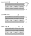
まず、図1に示すように、支持体金属箔(または金属層Cという場合がある。)12と剥離層14と金属層A11と剥離層13と金属層B10とを、この順に下側から積層した支持体金属箔付き複合金属層9を準備する。
金属層Bは、金属層A11の表面(金属層B10との界面)を保護するためのものであり、金属層A11との界面で物理的に剥離可能とされる。また、金属層B10と金属層A11との界面には、界面での剥離強度を安定化するための剥離層13が設けられる。剥離層としては、絶縁層と導体層とを積層する際の加熱・加圧を複数回行っても剥離強度が安定化しているものが好ましい。このような剥離層13としては、特許文献3及び4に開示されているような、Ni及びWの金属酸化物又はNi及びMoの金属酸化物を含有するものや、Cu-Ni-Mo合金からなるものなどが挙げられる。なお、この剥離層13は、金属層B10を金属層A11との界面で物理的に剥離する際には、金属層B10側に付着した状態で剥離し、金属層A11の表面には残留しないものが望ましい。
金属層A11は、金属層10を剥離した後の表面にパターンめっき18を行うために電流を供給する給電層となるものであり、金属層B10との界面および支持体金属箔(または金属層C)12との界面で物理的に剥離可能とされる。後述するように導体パターン2を形成する際(図8(16))にはエッチングで除去されるので、エッチング量のばらつきを極力低減して高精度な微細回路を形成するためには1μm~5μmの極薄金属箔が好ましく、3μm~5μmが特に好ましい。また、金属層B10との界面および支持体金属箔(または金属層C)12との界面には、界面での剥離強度を安定化するため、上述したような剥離層13、14を設けられる。
支持体金属箔(または金属層C)12は、支持体金属箔付き複合金属層9を基材16と積層して支持基板17を作成する際に、基材16と積層される側に配置するものであり、金属層A11との界面で物理的に剥離可能とされる。基材16と積層される際に、基材16との接着性を有していれば特に材質や厚みは問わないが、汎用性や取り扱い性の点で、材質としては銅箔やアルミニウム箔が好ましく、厚みとしては12μm~105μmが好ましく、35μm~70μmが特に好ましい。また、金属層A11との界面には、界面での剥離強度を安定化するため、上述したような剥離層14が設けられる。
支持体金属箔付き複合金属層9としては、3層以上の金属層(例えば、上述したように、金属層B10と金属層A11と支持体金属箔(または金属層C)12)を有し、少なくとも2箇所の界面(例えば、上述したように、金属層B10と金属層A11との界面および金属層A11と支持体金属箔(または金属層C)12との界面)が物理的に剥離可能なものを用いる。支持体金属箔付き複合金属層9の支持体金属箔(または金属層C)12側に基材16を積層して支持基板17を形成する工程の際には、金属層B10の表面に樹脂粉等の異物が付着することがあるが、このような異物が付着したとしても、金属層B10を金属層A11との界面で物理的に剥離することで、樹脂粉等の異物の影響のない金属層A11の表面が形成されるので、高品質な金属箔表面を確保することができる。したがって、金属層A11を給電層として使用してパターンめっき18を行う場合にも、欠陥の発生を抑制することができるので、歩留りの向上を図ることが可能になる。
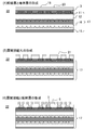
以下の図2~図8では、図1と同様に、金属層B10と金属層A11との間には剥離層13を、金属層A11と金属層C12との間に剥離層14を設けているが、図示を省略する。次に、図2(1)に示すように、支持体金属箔付き複合金属層9の支持体金属箔(または金属層C)12側と基材16とを積層して支持基板17を形成する。基材16は、支持体金属箔付き複合金属層9と積層一体化して支持基板17を形成するものであり、基材16としては、一般的に配線板の絶縁層3として使用されるものを用いることができる。また、支持体金属箔付き複合金属層9と基材16に加えて、金属箔15を積層一体化してもよい。このような基材16として、ガラスエポキシ、ガラスポリイミド等が挙げられる。支持基板17は、支持体金属箔付き複合金属層9を用いて、配線板を製造する際に剛性を確保することによって、作業性を向上させること、およびハンドリング時の損傷を防いで歩留りを向上させるのを主な役割とするものである。このため、基材16としては、ガラス繊維等の補強材を有するものが望ましく、例えば、ガラスエポキシ、ガラスポリイミド等のプリプレグを、支持体金属箔付き複合金属層9と重ねて、熱プレス等を用いて加熱・加圧して積層一体化することで形成できる。
次に、図2(2)に示すように、支持体金属箔付き複合金属層9の金属層B10と金属層A11との界面で、金属層B10を物理的に剥離する。金属層B10の表面には、積層時に基材16の材料となるプリプレグ等からの樹脂粉等の異物が付着する場合がある。このため、この金属層B10を用いて導体パターン2を形成する場合は、表面に付着した樹脂粉等の異物によって、導体パターン2に断線や短絡等の欠陥が生じることがあり、歩留りの低下に繋がる可能性がある。しかし、このように、金属層B10を剥離し除去することにより、樹脂粉等の異物が付着していない金属層A11を使用して導体パターンを形成することができるので、回路欠陥の発生を抑制することができ、歩留りを改善することが可能になる。また、金属層B10を物理的に剥離可能であるため、金属層B10と金属層A11との界面の剥離強度を調整することで、剥離作業を容易に行うことができる。
ここで、支持体金属箔付き複合金属層9は、金属層A11と支持体金属箔(または金属層C)12との界面の剥離強度が、金属層B10と金属層A11との界面の剥離強度よりも大きく形成されるのが望ましい。これにより、金属層B10と金属層A11との界面で物理的に剥離する際に、金属層A11と支持体金属箔(または金属層C)12との界面が同時に剥離するのを抑制することができる。剥離強度としては、加熱する前の初期において、金属層B10と金属層A11との界面では2N/m~50N/m、金属層A11と支持体金属箔(または金属層C)12との界面では10N/m~70N/mとし、金属層B10と金属層A11との界面の剥離強度が、金属層A11と支持体金属箔(または金属層C)12との界面の剥離強度よりも5N/m~20N/m小さくなるようにすると、製造工程でのハンドリングで剥離することがなく、一方で剥離する際は容易であり、しかも金属層B10を剥離する際に、金属層A11が同時に剥れるのを抑制することができるので作業性がよい。
剥離強度の調整は、例えば、特許文献3及び4に示されるように、剥離層となる金属酸化物や合金めっき層を形成するためのめっき液組成や条件を調整することにより可能となる。
次に、図2(3)に示すように、支持基板17に残った金属層A11上にパターンめっき18を行う。上述したように、金属層A11の表面(金属層B10との界面)には、積層時に使用するプリプレグ等からの樹脂粉等の異物は付着しないので、これに起因する回路欠陥を抑制可能となる。パターンめっき18は、金属層A11上に、めっきレジスト(図示しない。)を形成した後、電気めっきを用いて行うことができる。めっきレジストとしては、配線板の製造プロセスで用いられる感光性レジストを使用することができる。電気めっきとしては、配線板の製造プロセスで用いられる硫酸銅めっき等を用いることができる。
次に、図3(4)に示すように、パターンめっき18を含む金属層A11上に絶縁層3を積層して支持基板付き配線板22を形成する。このとき、同時に導体層20となる金属箔を積層してもよい。絶縁層3としては、一般的に配線板の絶縁層3として使用されるものを用いることができる。このような絶縁層3として、エポキシ系樹脂、ポリイミド系樹脂等が挙げられ、例えば、エポキシ系やポリイミド系の接着シート、ガラスエポキシやガラスポリイミド等のプリプレグを、熱プレス等を用いて加熱・加圧して積層一体化することで形成できる。導体層20となる金属箔としては、配線板の製造で用いられる銅箔が望ましい。
次に、図3(5)、(6)に示すように、層間接続孔21を形成し、層間接続5や配線層6を形成してもよい。層間接続5は、例えば、いわゆるコンフォーマル工法を用いて層間接続孔21を形成した後、この層間接続孔21内をめっきすることで形成することができる。このめっきには、下地めっきとして薄付け無電解銅めっきを行った後、厚付けめっきとして無電解銅めっきや電気銅めっき、フィルドビアめっき等を用いることができる。エッチングする導体層20の厚みを薄くして微細回路を形成し易くするためには、薄付けの下地めっきの後、めっきレジストを形成し、厚付けめっきを電気銅めっきやフィルドビアめっきで行うのが望ましい。配線層6は、例えば、層間接続孔21へのめっきを行った後、エッチングによって不要部分の導体層20を除去することにより形成することができる。
次に、図4(7)、(8)および図5(9)、(10)に示すように、配線層6や層間接続5の上に、さらに絶縁層3、導体層20、パターンめっき18を形成し、図3(5)、(6)のときと同様にして、所望の層数となるように、配線層6や層間接続5を形成することもできる。このようにして支持基板付き配線板22を形成することで、支持基板17が剛性を確保するため、作業性を向上させ、ハンドリング時の損傷を防いで歩留りを向上させることが可能になる。
次に、図6(11)、(12)に示すように、配線層6を形成した後、必要に応じて所望の箇所にソルダーレジシスト4や保護めっき8を形成する。保護めっき8としては、配線板の接続端子の保護めっき8として用いられるニッケルめっきと金めっきが望ましい。
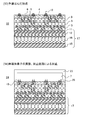
次に、図7(13)に示すように、必要に応じて再上層の配線層の所望の位置に、予備はんだ19を形成してもよい。予備はんだ19は、はんだペーストを印刷しリフローする方法などによって形成することができる。このように、支持基板付き配線板22の状態で、予備はんだの形成を行うことで、配線板単独では、はんだリフロー時の加熱で反りや変形を生じやすい場合でも、反りや変形を抑制可能となり、実装時の歩留まりが向上する。また、予備はんだ19を配線板側に設けることで、半導体素子7を実装する工程でのはんだ付与工程を省略することができ、工数低減が可能になる。
次に、図7(14)に示すように、半導体素子7の搭載(25はバンプ)及び封止樹脂23による封止を行い、支持基板付き半導体パッケージ24を形成する。このように、支持基板付き配線板22を用いて、支持基板17を設けたまま半導体素子7の搭載や封止を行うことで、配線板が薄く剛性を有しない場合や、反り・変形を生じやすい場合でも、支持基板17が剛性を確保し、反り・変形を抑制するので、実装歩留まりが改善する。
次に、図8(15)に示すように、支持基板付き半導体パッケージ24において、支持体金属箔付き複合金属層9の金属層A11と支持体金属箔(または金属層C)12との界面で、半導体パッケージ26を金属層A11とともに支持基板17から物理的に剥離して分離する。つまり、支持基板付き半導体パッケージ24から、支持基板17の金属層A11を半導体パッケージ26側に残して、金属層A11と金属層C12との間の剥離層14とともに支持基板17を剥離する。
次に、図8(16)に示すように、分離した半導体パッケージ26の底面に残った金属層A11をエッチング等により除去して、前記パターンめっき18を前記絶縁層3の表面に露出させ、導体パターン2を形成する。これにより、導体パターン2を形成する際に、導体パターン2の側面がエッチングによって侵食されないため、アンダーカットを生じないので、微細な導体パターン2を形成することができる。また、本発明で形成される導体パターン2は、絶縁層3に埋め込まれた状態となるため、導体パターン2の底面だけでなく、両側の側面も絶縁層3と密着しているため、微細回路であっても、十分な密着性を確保することができる。さらに、金属層A11として厚さ1μm~5μmの極薄銅箔を用いた場合は、僅かなエッチング量でも金属層A11を除去することができるため、絶縁層3に埋め込まれ、絶縁層3から露出した導体パターン2の表面は平坦であり、接続信頼性を確保することができ、接続端子として用いられるのにも適している。
以下、本発明を実施例によって具体的に説明するが、本発明はこれらの実施例に限定されるものではない。
1.支持体金属箔付き複合金属層の製造
支持体金属箔としては厚さ18μmの電解銅箔を用い、前処理として硫酸30g/Lにて酸洗浄を行い、次に光沢面の表面に剥離層を形成する(Ni30g/L、Mo3.0g/L、クエン酸30g/L)の組成を持つ浴にて金属酸化物層を形成させる。なお金属酸化物量の調整は電流で行う。
次に金属層であるが(硫酸銅200g/L、硫酸100g/L)の浴にて、電解めっきを行い5μmまでめっきを施した。
金属酸化物層及び金属層の形成を所定回数行った後、最上層にのみクロメート処理を行った。得られた支持体金属箔付き複合金属層の、金属層ごとの剥離強度を測定した。また、この支持体金属箔付き複合金属層を300℃で5時間加熱し、層ごとに剥離強度を測定し、その変化率を求めた。なお、剥離強度の調整は、金属酸化物層の厚さで行った。剥離強度の測定結果を表1に示す。
表1に示す支持体金属箔付き複合金属層A及びBは、具体的には以下の(実施例1)及び(実施例2)のようにして製造した。
支持体金属箔としては厚さ18μmの電解銅箔を用い、前処理として硫酸30g/Lにて酸洗浄を行い、次に光沢面の表面に剥離層を形成する(Ni30g/L、Mo3.0g/L、クエン酸30g/L)の組成を持つ浴にて金属酸化物層を形成させる。なお金属酸化物量の調整は電流で行う。
次に金属層であるが(硫酸銅200g/L、硫酸100g/L)の浴にて、電解めっきを行い5μmまでめっきを施した。
金属酸化物層及び金属層の形成を所定回数行った後、最上層にのみクロメート処理を行った。得られた支持体金属箔付き複合金属層の、金属層ごとの剥離強度を測定した。また、この支持体金属箔付き複合金属層を300℃で5時間加熱し、層ごとに剥離強度を測定し、その変化率を求めた。なお、剥離強度の調整は、金属酸化物層の厚さで行った。剥離強度の測定結果を表1に示す。
表1に示す支持体金属箔付き複合金属層A及びBは、具体的には以下の(実施例1)及び(実施例2)のようにして製造した。
(実施例1)
支持体金属箔付き複合金属層Aの製造
(1)支持体金属箔として厚さ18μmの電解銅箔を用い、硫酸30g/Lに60秒浸漬して酸洗浄後に流水で30秒間水洗を行った。
(2)洗浄した電解銅箔を陰極とし、酸化イリジウムコーテイングを施したTi極板を陽極として、硫酸ニッケル6水和物30g/L、モリブデン酸ナトリウム2水和物3.0g/L、クエン酸3ナトリウム2水和物30g/L、pH6.0、液温度30℃の浴にて電解銅箔の光沢面に電流密度20A/dm2で5秒間電解処理し、ニッケルとモリブデンからなる金属酸化物を含有する剥離層1を形成した。
(3)剥離層1を形成後の表面に、硫酸銅5水和物200g/L、硫酸100g/L、液温度40℃の浴にて、酸化イリジウムコーテイングを施したTi極板を陽極として、電流密度4A/dm2で340秒間電解めっきを行い厚さ5μmの金属層1を形成した。
(4)金属層1を形成後の表面に(2)と同様の浴を用いて、電流密度10A/dm2で10秒間電解処理し、ニッケルとモリブデンからなる金属酸化物を含有する剥離層2を形成した。
(5)剥離層2を形成後の表面に(3)と同様の浴を用いて、電流密度4A/dm2で340秒間電解めっきを行い厚さ5μmの金属層2を形成した。
(6)金属層2を形成後の表面に(2)と同様の浴を用いて、電流密度5A/dm2で20秒間電解処理し、ニッケルとモリブデンからなる金属酸化物を含有する剥離層3を形成した。
(7)剥離層3を形成後の表面に(3)と同様の浴を用いて、電流密度4A/dm2で340秒間電解めっきを行い厚さ5μmの金属層3を形成した。
(8)金属層3を形成後の表面に(2)と同様の浴を用いて、電流密度2A/dm2で50秒間電解処理し、ニッケルとモリブデンからなる金属酸化物を含有する剥離層4を形成した。
(9)剥離層4を形成後の表面に(3)と同様の浴を用いて、電流密度4A/dm2で340秒間電解めっきを行い厚さ5μmの金属層4を形成した。
(10)金属層4を形成後の表面に、硫酸銅5水和物150g/L、硫酸100g/L、液温度30℃に調整しためっき浴(限界電流密度15A/dm2)を用いて1電流密度30A/dm2で3秒間電解処理し、2電流密度5A/dm2で80秒間電解処理してコブ状の銅粒子からなる粗化層を形成した。
(11)次に粗化層を形成後の表面に、重クロム酸ナトリウム2水和物3.5g/L、pH4.0、液温度28℃に調整した水溶液を用いて電流密度0.5A/dm2で2.5秒間電解処理し、粗化層上にクロメート層を形成した。
(12)クロメート層を形成した表面に、3-グリシドキシプロピルトリメトキシシラン0.1質量%の水溶液に浸漬後、直ちに80℃で乾燥して、クロメート層上にシランカップリング剤処理層を形成した。
支持体金属箔付き複合金属層Aの製造
(1)支持体金属箔として厚さ18μmの電解銅箔を用い、硫酸30g/Lに60秒浸漬して酸洗浄後に流水で30秒間水洗を行った。
(2)洗浄した電解銅箔を陰極とし、酸化イリジウムコーテイングを施したTi極板を陽極として、硫酸ニッケル6水和物30g/L、モリブデン酸ナトリウム2水和物3.0g/L、クエン酸3ナトリウム2水和物30g/L、pH6.0、液温度30℃の浴にて電解銅箔の光沢面に電流密度20A/dm2で5秒間電解処理し、ニッケルとモリブデンからなる金属酸化物を含有する剥離層1を形成した。
(3)剥離層1を形成後の表面に、硫酸銅5水和物200g/L、硫酸100g/L、液温度40℃の浴にて、酸化イリジウムコーテイングを施したTi極板を陽極として、電流密度4A/dm2で340秒間電解めっきを行い厚さ5μmの金属層1を形成した。
(4)金属層1を形成後の表面に(2)と同様の浴を用いて、電流密度10A/dm2で10秒間電解処理し、ニッケルとモリブデンからなる金属酸化物を含有する剥離層2を形成した。
(5)剥離層2を形成後の表面に(3)と同様の浴を用いて、電流密度4A/dm2で340秒間電解めっきを行い厚さ5μmの金属層2を形成した。
(6)金属層2を形成後の表面に(2)と同様の浴を用いて、電流密度5A/dm2で20秒間電解処理し、ニッケルとモリブデンからなる金属酸化物を含有する剥離層3を形成した。
(7)剥離層3を形成後の表面に(3)と同様の浴を用いて、電流密度4A/dm2で340秒間電解めっきを行い厚さ5μmの金属層3を形成した。
(8)金属層3を形成後の表面に(2)と同様の浴を用いて、電流密度2A/dm2で50秒間電解処理し、ニッケルとモリブデンからなる金属酸化物を含有する剥離層4を形成した。
(9)剥離層4を形成後の表面に(3)と同様の浴を用いて、電流密度4A/dm2で340秒間電解めっきを行い厚さ5μmの金属層4を形成した。
(10)金属層4を形成後の表面に、硫酸銅5水和物150g/L、硫酸100g/L、液温度30℃に調整しためっき浴(限界電流密度15A/dm2)を用いて1電流密度30A/dm2で3秒間電解処理し、2電流密度5A/dm2で80秒間電解処理してコブ状の銅粒子からなる粗化層を形成した。
(11)次に粗化層を形成後の表面に、重クロム酸ナトリウム2水和物3.5g/L、pH4.0、液温度28℃に調整した水溶液を用いて電流密度0.5A/dm2で2.5秒間電解処理し、粗化層上にクロメート層を形成した。
(12)クロメート層を形成した表面に、3-グリシドキシプロピルトリメトキシシラン0.1質量%の水溶液に浸漬後、直ちに80℃で乾燥して、クロメート層上にシランカップリング剤処理層を形成した。
(実施例2)
支持体金属箔付き複合金属層Bの製造
(1)支持体金属箔として厚さ18μmの電解銅箔を用い、硫酸30g/Lに60秒浸漬して酸洗浄後に流水で30秒間水洗を行った。
(2)洗浄した電解銅箔を陰極とし、酸化イリジウムコーテイングを施したTi極板を陽極として、硫酸ニッケル6水和物30g/L、モリブデン酸ナトリウム2水和物3.0g/L、クエン酸3ナトリウム2水和物30g/L、pH6.0、液温度30℃の浴にて電解銅箔の光沢面に電流密度25A/dm2で4秒間電解処理し、ニッケルとモリブデンからなる金属酸化物を含有する剥離層1を形成した。
(3)剥離層1を形成後の表面に、硫酸銅5水和物200g/L、硫酸100g/L、液温度40℃の浴にて、酸化イリジウムコーテイングを施したTi極板を陽極として、電流密度4A/dm2で340秒間電解めっきを行い厚さ5μmの金属層1を形成した。
(4)金属層1を形成後の表面に(2)と同様の浴を用いて、電流密度20A/dm2で5秒間電解処理し、ニッケルとモリブデンからなる金属酸化物を含有する剥離層2を形成した。
(5)剥離層2を形成後の表面に(3)と同様の浴を用いて、電流密度4A/dm2で340秒間電解めっきを行い厚さ5μmの金属層2を形成した。
(6)金属層2を形成後の表面に(2)と同様の浴を用いて、電流密度10A/dm2で10秒間電解処理し、ニッケルとモリブデンからなる金属酸化物を含有する剥離層3を形成した。
(7)剥離層3を形成後の表面に(3)と同様の浴を用いて、電流密度4A/dm2で340秒間電解めっきを行い厚さ5μmの金属層3を形成した。
(8)金属層3を形成後の表面に(2)と同様の浴を用いて、電流密度2.5A/dm2で40秒間電解処理し、ニッケルとモリブデンからなる金属酸化物を含有する剥離層4を形成した。
(9)剥離層4を形成後の表面に(3)と同様の浴を用いて、電流密度4A/dm2で340秒間電解めっきを行い厚さ5μmの金属層4を形成した。
(10)金属層4の表面に実施例1の(10)から(12)と同様の処理を施し、粗化層、クロメート層およびシランカップリング剤処理層を順次形成した。
支持体金属箔付き複合金属層Bの製造
(1)支持体金属箔として厚さ18μmの電解銅箔を用い、硫酸30g/Lに60秒浸漬して酸洗浄後に流水で30秒間水洗を行った。
(2)洗浄した電解銅箔を陰極とし、酸化イリジウムコーテイングを施したTi極板を陽極として、硫酸ニッケル6水和物30g/L、モリブデン酸ナトリウム2水和物3.0g/L、クエン酸3ナトリウム2水和物30g/L、pH6.0、液温度30℃の浴にて電解銅箔の光沢面に電流密度25A/dm2で4秒間電解処理し、ニッケルとモリブデンからなる金属酸化物を含有する剥離層1を形成した。
(3)剥離層1を形成後の表面に、硫酸銅5水和物200g/L、硫酸100g/L、液温度40℃の浴にて、酸化イリジウムコーテイングを施したTi極板を陽極として、電流密度4A/dm2で340秒間電解めっきを行い厚さ5μmの金属層1を形成した。
(4)金属層1を形成後の表面に(2)と同様の浴を用いて、電流密度20A/dm2で5秒間電解処理し、ニッケルとモリブデンからなる金属酸化物を含有する剥離層2を形成した。
(5)剥離層2を形成後の表面に(3)と同様の浴を用いて、電流密度4A/dm2で340秒間電解めっきを行い厚さ5μmの金属層2を形成した。
(6)金属層2を形成後の表面に(2)と同様の浴を用いて、電流密度10A/dm2で10秒間電解処理し、ニッケルとモリブデンからなる金属酸化物を含有する剥離層3を形成した。
(7)剥離層3を形成後の表面に(3)と同様の浴を用いて、電流密度4A/dm2で340秒間電解めっきを行い厚さ5μmの金属層3を形成した。
(8)金属層3を形成後の表面に(2)と同様の浴を用いて、電流密度2.5A/dm2で40秒間電解処理し、ニッケルとモリブデンからなる金属酸化物を含有する剥離層4を形成した。
(9)剥離層4を形成後の表面に(3)と同様の浴を用いて、電流密度4A/dm2で340秒間電解めっきを行い厚さ5μmの金属層4を形成した。
(10)金属層4の表面に実施例1の(10)から(12)と同様の処理を施し、粗化層、クロメート層およびシランカップリング剤処理層を順次形成した。
2.剥離性の評価
最上層表面を硫酸で洗浄、表面の水分を除去し、ポリイミド前駆体(宇部興産株式会社製商品名:U-ワニス-A)を厚さ50μmで塗布し、予備乾燥後に300℃で2時間キュアして、ポリイミドとした。ついで、この金属層付きポリイミドを下層の金属層から剥離した。さらに、この露出した金属層に同様にポリイミドを形成し、順次剥離を繰り返した。剥離性を目視で評価した結果を表1に示す。
最上層表面を硫酸で洗浄、表面の水分を除去し、ポリイミド前駆体(宇部興産株式会社製商品名:U-ワニス-A)を厚さ50μmで塗布し、予備乾燥後に300℃で2時間キュアして、ポリイミドとした。ついで、この金属層付きポリイミドを下層の金属層から剥離した。さらに、この露出した金属層に同様にポリイミドを形成し、順次剥離を繰り返した。剥離性を目視で評価した結果を表1に示す。

3.配線板の製造
(実施例3)
まず、図1に示すように、支持体金属箔(または金属層Cという場合がある。)12と剥離層14と金属層A11と剥離層13と金属層B10とを、この順に下側から積層した支持体金属箔付き複合金属層9を準備した。この実施例では、表1の支持体金属箔付き複合金属層9と同様の条件で支持体金属箔付き複合金属層9を作製したが、金属層の数は、支持体金属箔(金属層C)12と金属層A11と金属層B10の3層である。各金属層の剥離強度は、表1の支持体金属箔付き複合金属層9の製造条件を参考にして調整した。金属層の剥離強度としては、加熱する前の初期において、金属層B10と金属層A11との界面では2N/m~50N/m、金属層A11と支持体金属箔(または金属層C)12との界面では10N/m~70N/mとし、金属層B10と金属層A11との界面の剥離強度が、金属層A11と支持体金属箔(または金属層C)12との界面の剥離強度よりも5N/m~20N/m小さくなるようにした。
(実施例3)
まず、図1に示すように、支持体金属箔(または金属層Cという場合がある。)12と剥離層14と金属層A11と剥離層13と金属層B10とを、この順に下側から積層した支持体金属箔付き複合金属層9を準備した。この実施例では、表1の支持体金属箔付き複合金属層9と同様の条件で支持体金属箔付き複合金属層9を作製したが、金属層の数は、支持体金属箔(金属層C)12と金属層A11と金属層B10の3層である。各金属層の剥離強度は、表1の支持体金属箔付き複合金属層9の製造条件を参考にして調整した。金属層の剥離強度としては、加熱する前の初期において、金属層B10と金属層A11との界面では2N/m~50N/m、金属層A11と支持体金属箔(または金属層C)12との界面では10N/m~70N/mとし、金属層B10と金属層A11との界面の剥離強度が、金属層A11と支持体金属箔(または金属層C)12との界面の剥離強度よりも5N/m~20N/m小さくなるようにした。
以下の図2~図8では、図1と同様に、金属層B10と金属層A11との間には剥離層13を、金属層A11と金属層C12との間に剥離層14を設けているが、図示を省略する。次に、図2(1)に示すように、支持体金属箔付き複合金属層9の支持体金属箔(または金属層C)12側と、基材16となるガラスエポキシ製のプリプレグと、金属箔15となる銅箔とを、熱プレスを用いて積層し、支持基板17を形成した。
次に、図2(2)に示すように、支持体金属箔付き複合金属層9の金属層B10と金属層A11との界面で、金属層B10を物理的に剥離した。金属層B10の表面には、積層時に基材16の材料となるプリプレグ等からの樹脂粉等の異物が付着していたが、金属層B10を剥離し除去することにより、樹脂粉等の異物が付着していない金属層A11を準備することができた。
次に、図2(3)に示すように、支持基板17に残った金属層A11上に、感光性のめっきレジストを形成し、硫酸銅電気めっきを用いてパターンめっき18を行った。
次に、図3(4)に示すように、パターンめっき18を含む金属層A11上に、エポキシ系の接着シートと銅箔とを熱プレスで積層して絶縁層3と導体層20とを形成し、支持基板付き配線板22を作製した。
次に、図3(5)、(6)に示すように、コンフォーマル工法を用いて層間接続孔21を形成した後、この層間接続孔21内に薄付け無電解銅めっきを行った後、めっきレジストを形成してパターン電気銅めっきを行い、めっきレジスト剥離後にエッチングによって余分な箇所の導体層20を除去することで、層間接続5と配線層6を形成した。
次に、図4(7)、(8)および図5(9)、(10)に示すように、配線層6や層間接続5の上に、さらに絶縁層3、導体層20、パターンめっき18を形成し、図3(5)、(6)のときと同様にして、所望の層数となるように、配線層6や層間接続5を形成した。
次に、図6(11)、(12)に示すように、配線層6を形成した後、ソルダーレジシスト4と保護めっき8を形成した。保護めっき8としては、配線板の接続端子の保護めっき8として用いられるニッケルめっきと金めっきを用いた。
次に、図7(13)に示すように、再上層の配線層6の所定の位置に、予備はんだ19を形成した。予備はんだ19は、はんだペーストを印刷しリフローする方法によって形成した。
4.半導体パッケージの製造
(実施例4)
次に、図7(14)に示すように、半導体素子7の搭載及び封止樹脂23による封止を行い、支持基板付き半導体パッケージ24を形成した。
(実施例4)
次に、図7(14)に示すように、半導体素子7の搭載及び封止樹脂23による封止を行い、支持基板付き半導体パッケージ24を形成した。
次に、図8(15)に示すように、支持基板付き半導体パッケージ24において、支持体金属箔付き複合金属層9の金属層A11と支持体金属箔(または金属層C)12との界面で、半導体パッケージ26を金属層A11とともに支持基板17から物理的に剥離して分離した。つまり、支持基板付き半導体パッケージ24から、支持基板17の金属層A11を半導体パッケージ26側に残して、金属層A11と金属層C12との間の剥離層14とともに支持基板17を剥離した。
次に、図8(16)に示すように、分離した半導体パッケージ26の底面に残った金属層A11をエッチング等により除去して、前記パターンめっき18を前記絶縁層3の表面に露出させ、導体パターン2を形成した。
2:導体パターン
3:絶縁層
4:ソルダーレジスト
5:層間接続
6:配線層
7:半導体素子
8:保護めっき
9:支持体金属箔付き複合金属層
10:金属層B
11:金属層A
12:支持体金属箔又は金属層C
13:剥離層
14:剥離層
15:金属箔
16:基材
17:支持基板
18:パターンめっき
19:予備はんだ
20:導体層
21:層間接続孔
22:支持基板付き配線板
23:封止樹脂
24:支持基板付き半導体パッケージ
25:バンプ
26:半導体パッケージ
3:絶縁層
4:ソルダーレジスト
5:層間接続
6:配線層
7:半導体素子
8:保護めっき
9:支持体金属箔付き複合金属層
10:金属層B
11:金属層A
12:支持体金属箔又は金属層C
13:剥離層
14:剥離層
15:金属箔
16:基材
17:支持基板
18:パターンめっき
19:予備はんだ
20:導体層
21:層間接続孔
22:支持基板付き配線板
23:封止樹脂
24:支持基板付き半導体パッケージ
25:バンプ
26:半導体パッケージ
Claims (8)
- 支持体金属箔である最下層金属層と2層以上の金属層とからなる複数の金属層が、隣合った金属層間に剥離層を介して積層されてなる支持体金属箔付き複合金属層であって、最下層金属層と最上層の金属層との間に位置する各金属層Aと、その上面の剥離層を介して隣接する金属層Bとの間の剥離強度が、金属層Aと、その下面の剥離層を介して隣接する金属層Cとの間の剥離強度よりも小さいことを特徴とする支持体金属箔付き複合金属層。
- 最下層金属層と最上層の金属層との間に位置する各金属層Aと、その上面の剥離層を介して隣接する金属層とBとの間の剥離強度が、金属層Aと、その下面の剥離層を介して隣接する金属層Cとの間の剥離強度よりも、5N/mから20N/m小さいことを特徴とする請求項1に記載の支持体金属箔付き複合金属層。
- 剥離層を介して隣接する2つの金属層間の剥離強度の300℃で5時間加熱した前後の変化率が25%以下であることを特徴とする請求項1または2に記載の支持体金属箔付き複合金属層。
- 請求項1から3の何れかに記載の支持体金属箔付き複合金属層の最上層の金属層上にパターンめっきを行い(イ)、このパターンめっきを含む金属層上にポリイミド前駆体を塗布し(ロ)、予備乾燥とキュアを行ってポリイミドとした後(ハ)、この金属層付きポリイミドを前記最上層の下層の金属層から剥離し(ニ)、この金属層付きポリイミドに残った金属層を除去して前記パターンめっきをポリイミドから露出させ、導体パターンを形成し(ホ)、前記金属層付きポリイミドを剥離した後に残った支持体金属箔付き複合金属層の最上層表面に対して、上記(イ)から(ホ)を順次繰り返し、複数枚の配線板を形成することを特徴とする配線板の製造方法。
- 請求項1から3の何れかに記載の支持体金属箔付き複合金属層であって、支持体金属箔である金属層C、金属層Cに剥離層を介して隣接する金属層A、及び、金属層Aに剥離層を介して隣接する金属層Bを有する支持体金属箔付き複合金属層の支持体金属箔側と基材とを積層して支持基板を形成する工程と、金属層Bと金属層Aとの間の剥離層とともに、前記金属層Aの表面から金属層Bを剥離する工程と、前記支持基板に残った金属層A上にパターンめっきを行う工程と、前記パターンめっきを含む金属層A上に絶縁層と配線層を形成して、支持基板付き配線板を形成する工程と、を有する配線板の製造方法。
- 請求項5に記載の配線板の製造方法において、支持基板付き配線板を形成する工程の後、さらに最上層の配線層に予備はんだを形成する工程を有することを特徴とする配線板の製造方法。
- 請求項5または6に記載の配線板の製造方法によって製造された支持基板付き配線板。
- 請求項5または6に記載の配線板の製造方法によって製造された支持基板付き配線板に半導体素子を搭載し封止して、支持基板付き半導体パッケージを形成する工程と、前記支持基板付き半導体パッケージから、支持基板の金属層Aを半導体パッケージ側に残して、金属層Aと金属層Cとの間の剥離層とともに支持基板を剥離する工程と、前記半導体パッケージ側に残った金属層Aを除去してパターンめっきを絶縁層の表面に露出させ、導体パターンを形成する工程と、を有する半導体パッケージの製造方法。
Priority Applications (1)
| Application Number | Priority Date | Filing Date | Title |
|---|---|---|---|
| KR1020127020047A KR101423852B1 (ko) | 2010-03-30 | 2011-03-28 | 지지체 금속박 부착 복합 금속층, 이것을 이용한 배선판과 그 제조방법, 이 배선판을 이용한 반도체 패키지의 제조방법 |
Applications Claiming Priority (4)
| Application Number | Priority Date | Filing Date | Title |
|---|---|---|---|
| JP2010077334 | 2010-03-30 | ||
| JP2010-077334 | 2010-03-30 | ||
| JP2010198620A JP5473838B2 (ja) | 2010-03-30 | 2010-09-06 | 支持体金属箔付き複合金属層、これを用いた配線板とその製造方法、この配線板を用いた半導体パッケージの製造方法 |
| JP2010-198620 | 2010-09-06 |
Publications (1)
| Publication Number | Publication Date |
|---|---|
| WO2011122532A1 true WO2011122532A1 (ja) | 2011-10-06 |
Family
ID=44712228
Family Applications (1)
| Application Number | Title | Priority Date | Filing Date |
|---|---|---|---|
| PCT/JP2011/057556 Ceased WO2011122532A1 (ja) | 2010-03-30 | 2011-03-28 | 支持体金属箔付き複合金属層、これを用いた配線板とその製造方法、この配線板を用いた半導体パッケージの製造方法 |
Country Status (4)
| Country | Link |
|---|---|
| JP (1) | JP5473838B2 (ja) |
| KR (1) | KR101423852B1 (ja) |
| TW (1) | TWI516178B (ja) |
| WO (1) | WO2011122532A1 (ja) |
Cited By (2)
| Publication number | Priority date | Publication date | Assignee | Title |
|---|---|---|---|---|
| JP2015073068A (ja) * | 2013-10-01 | 2015-04-16 | 旭徳科技股▲ふん▼有限公司 | パッケージキャリア |
| JP2017011118A (ja) * | 2015-06-23 | 2017-01-12 | 日立化成株式会社 | 基板製造用キャリア部材及び基板の製造方法 |
Families Citing this family (7)
| Publication number | Priority date | Publication date | Assignee | Title |
|---|---|---|---|---|
| JP5672524B2 (ja) * | 2010-07-02 | 2015-02-18 | 日立化成株式会社 | 半導体素子搭載用パッケージ基板の製造方法 |
| JP5903920B2 (ja) * | 2012-02-16 | 2016-04-13 | 富士通株式会社 | 半導体装置の製造方法及び電子装置の製造方法 |
| KR20160089364A (ko) * | 2013-11-22 | 2016-07-27 | 미쓰이금속광업주식회사 | 매설 회로를 구비하는 프린트 배선판의 제조 방법 및 그 제조 방법으로 얻어지는 프린트 배선판 |
| JP6880661B2 (ja) * | 2016-11-04 | 2021-06-02 | 昭和電工マテリアルズ株式会社 | 半導体用仮固定材及びそれを用いた半導体装置の製造方法。 |
| WO2022102182A1 (ja) * | 2020-11-11 | 2022-05-19 | 三井金属鉱業株式会社 | 配線基板の製造方法 |
| CN114864799B (zh) * | 2021-02-04 | 2025-02-14 | 欣兴电子股份有限公司 | 封装结构及其制作方法 |
| TWI759095B (zh) | 2021-02-04 | 2022-03-21 | 欣興電子股份有限公司 | 封裝結構及其製作方法 |
Citations (5)
| Publication number | Priority date | Publication date | Assignee | Title |
|---|---|---|---|---|
| JPH02113591A (ja) * | 1988-10-22 | 1990-04-25 | Matsushita Electric Works Ltd | 印刷配線板の製造方法 |
| JPH0955575A (ja) * | 1995-08-10 | 1997-02-25 | Mitsui Toatsu Chem Inc | 積層体 |
| DE19910482A1 (de) * | 1999-03-10 | 2000-05-04 | Stp Elektronische Systeme Gmbh | Verfahren zur Herstellung von Leiterplatten-Schaltungsebenen |
| JP2005260058A (ja) * | 2004-03-12 | 2005-09-22 | Furukawa Circuit Foil Kk | キャリア付き極薄銅箔、キャリア付き極薄銅箔の製造方法および配線板 |
| WO2007135972A1 (ja) * | 2006-05-19 | 2007-11-29 | Mitsui Mining & Smelting Co., Ltd. | キャリアシート付銅箔、キャリアシート付銅箔の製造方法、キャリアシート付表面処理銅箔及びそのキャリアシート付表面処理銅箔を用いた銅張積層板 |
-
2010
- 2010-09-06 JP JP2010198620A patent/JP5473838B2/ja active Active
-
2011
- 2011-03-28 KR KR1020127020047A patent/KR101423852B1/ko active Active
- 2011-03-28 WO PCT/JP2011/057556 patent/WO2011122532A1/ja not_active Ceased
- 2011-03-30 TW TW100110996A patent/TWI516178B/zh active
Patent Citations (5)
| Publication number | Priority date | Publication date | Assignee | Title |
|---|---|---|---|---|
| JPH02113591A (ja) * | 1988-10-22 | 1990-04-25 | Matsushita Electric Works Ltd | 印刷配線板の製造方法 |
| JPH0955575A (ja) * | 1995-08-10 | 1997-02-25 | Mitsui Toatsu Chem Inc | 積層体 |
| DE19910482A1 (de) * | 1999-03-10 | 2000-05-04 | Stp Elektronische Systeme Gmbh | Verfahren zur Herstellung von Leiterplatten-Schaltungsebenen |
| JP2005260058A (ja) * | 2004-03-12 | 2005-09-22 | Furukawa Circuit Foil Kk | キャリア付き極薄銅箔、キャリア付き極薄銅箔の製造方法および配線板 |
| WO2007135972A1 (ja) * | 2006-05-19 | 2007-11-29 | Mitsui Mining & Smelting Co., Ltd. | キャリアシート付銅箔、キャリアシート付銅箔の製造方法、キャリアシート付表面処理銅箔及びそのキャリアシート付表面処理銅箔を用いた銅張積層板 |
Cited By (3)
| Publication number | Priority date | Publication date | Assignee | Title |
|---|---|---|---|---|
| JP2015073068A (ja) * | 2013-10-01 | 2015-04-16 | 旭徳科技股▲ふん▼有限公司 | パッケージキャリア |
| US9433099B2 (en) | 2013-10-01 | 2016-08-30 | Subtron Technology Co., Ltd. | Package carrier |
| JP2017011118A (ja) * | 2015-06-23 | 2017-01-12 | 日立化成株式会社 | 基板製造用キャリア部材及び基板の製造方法 |
Also Published As
| Publication number | Publication date |
|---|---|
| JP2011228613A (ja) | 2011-11-10 |
| TW201212743A (en) | 2012-03-16 |
| TWI516178B (zh) | 2016-01-01 |
| JP5473838B2 (ja) | 2014-04-16 |
| KR101423852B1 (ko) | 2014-07-25 |
| KR20120115351A (ko) | 2012-10-17 |
Similar Documents
| Publication | Publication Date | Title |
|---|---|---|
| JP5473838B2 (ja) | 支持体金属箔付き複合金属層、これを用いた配線板とその製造方法、この配線板を用いた半導体パッケージの製造方法 | |
| JP5896200B2 (ja) | 半導体素子搭載用パッケージ基板の製造方法 | |
| JP6377660B2 (ja) | 多層プリント配線板の製造方法 | |
| JP5859155B1 (ja) | 複合金属箔及びその製造方法並びにプリント配線板 | |
| CN103443916B (zh) | 半导体元件搭载用封装基板的制造方法、半导体元件搭载用封装基板以及半导体封装 | |
| CN101827495B (zh) | 复合金属箔及其制造方法以及印刷布线板 | |
| CN102714915B (zh) | 电子电路及其形成方法以及电子电路形成用覆铜层压板 | |
| JPWO2015122258A1 (ja) | キャリア付き極薄銅箔、並びにこれを用いて作製された銅張積層板、プリント配線基板及びコアレス基板 | |
| JPWO2012133637A1 (ja) | 多層プリント配線板の製造方法及びその製造方法で得られる多層プリント配線板 | |
| TWI593830B (zh) | With a carrier of ultra-thin copper foil, copper-clad laminate and coreless substrate | |
| TW201822606A (zh) | 複合金屬箔、使用該複合金屬箔的覆銅層疊板及該覆銅層疊板的製造方法 | |
| CN102265712B (zh) | 电子电路的形成方法 | |
| WO2012039285A1 (ja) | プリント配線板用銅箔の製造方法及びプリント配線板用銅箔 | |
| JP2012216824A (ja) | 半導体素子搭載用パッケージ基板の製造方法 | |
| CN108029202A (zh) | 印刷电路板的制造方法 | |
| WO2010018790A1 (ja) | マルチ導通部を有する多層積層回路基板 | |
| JP5672524B2 (ja) | 半導体素子搭載用パッケージ基板の製造方法 | |
| JP5716948B2 (ja) | 半導体素子搭載用パッケージ基板の製造方法 | |
| WO2012132578A1 (ja) | 銅キャリア付銅箔、その製造方法、電子回路用銅箔、その製造方法及び電子回路の形成方法 | |
| JP2014072326A (ja) | 半導体素子搭載用パッケージ基板及びその製造方法 | |
| WO2010021278A1 (ja) | 熱膨張係数の異なる樹脂フィルムを積層させた多層積層回路基板 |
Legal Events
| Date | Code | Title | Description |
|---|---|---|---|
| 121 | Ep: the epo has been informed by wipo that ep was designated in this application |
Ref document number: 11762756 Country of ref document: EP Kind code of ref document: A1 |
|
| ENP | Entry into the national phase |
Ref document number: 20127020047 Country of ref document: KR Kind code of ref document: A |
|
| NENP | Non-entry into the national phase |
Ref country code: DE |
|
| 122 | Ep: pct application non-entry in european phase |
Ref document number: 11762756 Country of ref document: EP Kind code of ref document: A1 |