WO2011121756A1 - 半導体装置およびその製造方法 - Google Patents
半導体装置およびその製造方法 Download PDFInfo
- Publication number
- WO2011121756A1 WO2011121756A1 PCT/JP2010/055847 JP2010055847W WO2011121756A1 WO 2011121756 A1 WO2011121756 A1 WO 2011121756A1 JP 2010055847 W JP2010055847 W JP 2010055847W WO 2011121756 A1 WO2011121756 A1 WO 2011121756A1
- Authority
- WO
- WIPO (PCT)
- Prior art keywords
- chip
- semiconductor device
- digging
- paste
- semiconductor chip
- Prior art date
- Legal status (The legal status is an assumption and is not a legal conclusion. Google has not performed a legal analysis and makes no representation as to the accuracy of the status listed.)
- Ceased
Links
Images























Classifications
-
- H—ELECTRICITY
- H10—SEMICONDUCTOR DEVICES; ELECTRIC SOLID-STATE DEVICES NOT OTHERWISE PROVIDED FOR
- H10W—GENERIC PACKAGES, INTERCONNECTIONS, CONNECTORS OR OTHER CONSTRUCTIONAL DETAILS OF DEVICES COVERED BY CLASS H10
- H10W70/00—Package substrates; Interposers; Redistribution layers [RDL]
- H10W70/40—Leadframes
- H10W70/464—Additional interconnections in combination with leadframes
- H10W70/466—Tape carriers or flat leads
-
- H—ELECTRICITY
- H10—SEMICONDUCTOR DEVICES; ELECTRIC SOLID-STATE DEVICES NOT OTHERWISE PROVIDED FOR
- H10W—GENERIC PACKAGES, INTERCONNECTIONS, CONNECTORS OR OTHER CONSTRUCTIONAL DETAILS OF DEVICES COVERED BY CLASS H10
- H10W70/00—Package substrates; Interposers; Redistribution layers [RDL]
- H10W70/40—Leadframes
- H10W70/481—Leadframes for devices being provided for in groups H10D8/00 - H10D48/00
-
- H—ELECTRICITY
- H10—SEMICONDUCTOR DEVICES; ELECTRIC SOLID-STATE DEVICES NOT OTHERWISE PROVIDED FOR
- H10W—GENERIC PACKAGES, INTERCONNECTIONS, CONNECTORS OR OTHER CONSTRUCTIONAL DETAILS OF DEVICES COVERED BY CLASS H10
- H10W90/00—Package configurations
- H10W90/811—Multiple chips on leadframes
-
- H—ELECTRICITY
- H10—SEMICONDUCTOR DEVICES; ELECTRIC SOLID-STATE DEVICES NOT OTHERWISE PROVIDED FOR
- H10W—GENERIC PACKAGES, INTERCONNECTIONS, CONNECTORS OR OTHER CONSTRUCTIONAL DETAILS OF DEVICES COVERED BY CLASS H10
- H10W70/00—Package substrates; Interposers; Redistribution layers [RDL]
- H10W70/40—Leadframes
- H10W70/411—Chip-supporting parts, e.g. die pads
- H10W70/417—Bonding materials between chips and die pads
-
- H—ELECTRICITY
- H10—SEMICONDUCTOR DEVICES; ELECTRIC SOLID-STATE DEVICES NOT OTHERWISE PROVIDED FOR
- H10W—GENERIC PACKAGES, INTERCONNECTIONS, CONNECTORS OR OTHER CONSTRUCTIONAL DETAILS OF DEVICES COVERED BY CLASS H10
- H10W72/00—Interconnections or connectors in packages
- H10W72/01—Manufacture or treatment
- H10W72/011—Apparatus therefor
- H10W72/0113—Apparatus for manufacturing die-attach connectors
-
- H—ELECTRICITY
- H10—SEMICONDUCTOR DEVICES; ELECTRIC SOLID-STATE DEVICES NOT OTHERWISE PROVIDED FOR
- H10W—GENERIC PACKAGES, INTERCONNECTIONS, CONNECTORS OR OTHER CONSTRUCTIONAL DETAILS OF DEVICES COVERED BY CLASS H10
- H10W72/00—Interconnections or connectors in packages
- H10W72/01—Manufacture or treatment
- H10W72/013—Manufacture or treatment of die-attach connectors
- H10W72/01308—Manufacture or treatment of die-attach connectors using permanent auxiliary members, e.g. using alignment marks
-
- H—ELECTRICITY
- H10—SEMICONDUCTOR DEVICES; ELECTRIC SOLID-STATE DEVICES NOT OTHERWISE PROVIDED FOR
- H10W—GENERIC PACKAGES, INTERCONNECTIONS, CONNECTORS OR OTHER CONSTRUCTIONAL DETAILS OF DEVICES COVERED BY CLASS H10
- H10W72/00—Interconnections or connectors in packages
- H10W72/01—Manufacture or treatment
- H10W72/019—Manufacture or treatment of bond pads
- H10W72/01931—Manufacture or treatment of bond pads using blanket deposition
- H10W72/01936—Manufacture or treatment of bond pads using blanket deposition in solid form, e.g. by using a powder or by laminating a foil
-
- H—ELECTRICITY
- H10—SEMICONDUCTOR DEVICES; ELECTRIC SOLID-STATE DEVICES NOT OTHERWISE PROVIDED FOR
- H10W—GENERIC PACKAGES, INTERCONNECTIONS, CONNECTORS OR OTHER CONSTRUCTIONAL DETAILS OF DEVICES COVERED BY CLASS H10
- H10W72/00—Interconnections or connectors in packages
- H10W72/071—Connecting or disconnecting
- H10W72/073—Connecting or disconnecting of die-attach connectors
-
- H—ELECTRICITY
- H10—SEMICONDUCTOR DEVICES; ELECTRIC SOLID-STATE DEVICES NOT OTHERWISE PROVIDED FOR
- H10W—GENERIC PACKAGES, INTERCONNECTIONS, CONNECTORS OR OTHER CONSTRUCTIONAL DETAILS OF DEVICES COVERED BY CLASS H10
- H10W72/00—Interconnections or connectors in packages
- H10W72/071—Connecting or disconnecting
- H10W72/073—Connecting or disconnecting of die-attach connectors
- H10W72/07311—Treating the bonding area before connecting, e.g. by applying flux or cleaning
-
- H—ELECTRICITY
- H10—SEMICONDUCTOR DEVICES; ELECTRIC SOLID-STATE DEVICES NOT OTHERWISE PROVIDED FOR
- H10W—GENERIC PACKAGES, INTERCONNECTIONS, CONNECTORS OR OTHER CONSTRUCTIONAL DETAILS OF DEVICES COVERED BY CLASS H10
- H10W72/00—Interconnections or connectors in packages
- H10W72/071—Connecting or disconnecting
- H10W72/073—Connecting or disconnecting of die-attach connectors
- H10W72/07331—Connecting techniques
-
- H—ELECTRICITY
- H10—SEMICONDUCTOR DEVICES; ELECTRIC SOLID-STATE DEVICES NOT OTHERWISE PROVIDED FOR
- H10W—GENERIC PACKAGES, INTERCONNECTIONS, CONNECTORS OR OTHER CONSTRUCTIONAL DETAILS OF DEVICES COVERED BY CLASS H10
- H10W72/00—Interconnections or connectors in packages
- H10W72/071—Connecting or disconnecting
- H10W72/073—Connecting or disconnecting of die-attach connectors
- H10W72/07331—Connecting techniques
- H10W72/07336—Soldering or alloying
-
- H—ELECTRICITY
- H10—SEMICONDUCTOR DEVICES; ELECTRIC SOLID-STATE DEVICES NOT OTHERWISE PROVIDED FOR
- H10W—GENERIC PACKAGES, INTERCONNECTIONS, CONNECTORS OR OTHER CONSTRUCTIONAL DETAILS OF DEVICES COVERED BY CLASS H10
- H10W72/00—Interconnections or connectors in packages
- H10W72/071—Connecting or disconnecting
- H10W72/073—Connecting or disconnecting of die-attach connectors
- H10W72/07331—Connecting techniques
- H10W72/07337—Connecting techniques using a polymer adhesive, e.g. an adhesive based on silicone or epoxy
-
- H—ELECTRICITY
- H10—SEMICONDUCTOR DEVICES; ELECTRIC SOLID-STATE DEVICES NOT OTHERWISE PROVIDED FOR
- H10W—GENERIC PACKAGES, INTERCONNECTIONS, CONNECTORS OR OTHER CONSTRUCTIONAL DETAILS OF DEVICES COVERED BY CLASS H10
- H10W72/00—Interconnections or connectors in packages
- H10W72/071—Connecting or disconnecting
- H10W72/075—Connecting or disconnecting of bond wires
-
- H—ELECTRICITY
- H10—SEMICONDUCTOR DEVICES; ELECTRIC SOLID-STATE DEVICES NOT OTHERWISE PROVIDED FOR
- H10W—GENERIC PACKAGES, INTERCONNECTIONS, CONNECTORS OR OTHER CONSTRUCTIONAL DETAILS OF DEVICES COVERED BY CLASS H10
- H10W72/00—Interconnections or connectors in packages
- H10W72/071—Connecting or disconnecting
- H10W72/075—Connecting or disconnecting of bond wires
- H10W72/07531—Techniques
- H10W72/07532—Compression bonding, e.g. thermocompression bonding
- H10W72/07533—Ultrasonic bonding, e.g. thermosonic bonding
-
- H—ELECTRICITY
- H10—SEMICONDUCTOR DEVICES; ELECTRIC SOLID-STATE DEVICES NOT OTHERWISE PROVIDED FOR
- H10W—GENERIC PACKAGES, INTERCONNECTIONS, CONNECTORS OR OTHER CONSTRUCTIONAL DETAILS OF DEVICES COVERED BY CLASS H10
- H10W72/00—Interconnections or connectors in packages
- H10W72/071—Connecting or disconnecting
- H10W72/075—Connecting or disconnecting of bond wires
- H10W72/07551—Connecting or disconnecting of bond wires characterised by changes in properties of the bond wires during the connecting
- H10W72/07554—Connecting or disconnecting of bond wires characterised by changes in properties of the bond wires during the connecting changes in dispositions
-
- H—ELECTRICITY
- H10—SEMICONDUCTOR DEVICES; ELECTRIC SOLID-STATE DEVICES NOT OTHERWISE PROVIDED FOR
- H10W—GENERIC PACKAGES, INTERCONNECTIONS, CONNECTORS OR OTHER CONSTRUCTIONAL DETAILS OF DEVICES COVERED BY CLASS H10
- H10W72/00—Interconnections or connectors in packages
- H10W72/071—Connecting or disconnecting
- H10W72/076—Connecting or disconnecting of strap connectors
-
- H—ELECTRICITY
- H10—SEMICONDUCTOR DEVICES; ELECTRIC SOLID-STATE DEVICES NOT OTHERWISE PROVIDED FOR
- H10W—GENERIC PACKAGES, INTERCONNECTIONS, CONNECTORS OR OTHER CONSTRUCTIONAL DETAILS OF DEVICES COVERED BY CLASS H10
- H10W72/00—Interconnections or connectors in packages
- H10W72/071—Connecting or disconnecting
- H10W72/076—Connecting or disconnecting of strap connectors
- H10W72/07631—Techniques
- H10W72/07632—Compression bonding, e.g. thermocompression bonding
- H10W72/07633—Ultrasonic bonding, e.g. thermosonic bonding
-
- H—ELECTRICITY
- H10—SEMICONDUCTOR DEVICES; ELECTRIC SOLID-STATE DEVICES NOT OTHERWISE PROVIDED FOR
- H10W—GENERIC PACKAGES, INTERCONNECTIONS, CONNECTORS OR OTHER CONSTRUCTIONAL DETAILS OF DEVICES COVERED BY CLASS H10
- H10W72/00—Interconnections or connectors in packages
- H10W72/071—Connecting or disconnecting
- H10W72/076—Connecting or disconnecting of strap connectors
- H10W72/07651—Connecting or disconnecting of strap connectors characterised by changes in properties of the strap connectors during connecting
- H10W72/07653—Connecting or disconnecting of strap connectors characterised by changes in properties of the strap connectors during connecting changes in shapes
-
- H—ELECTRICITY
- H10—SEMICONDUCTOR DEVICES; ELECTRIC SOLID-STATE DEVICES NOT OTHERWISE PROVIDED FOR
- H10W—GENERIC PACKAGES, INTERCONNECTIONS, CONNECTORS OR OTHER CONSTRUCTIONAL DETAILS OF DEVICES COVERED BY CLASS H10
- H10W72/00—Interconnections or connectors in packages
- H10W72/30—Die-attach connectors
-
- H—ELECTRICITY
- H10—SEMICONDUCTOR DEVICES; ELECTRIC SOLID-STATE DEVICES NOT OTHERWISE PROVIDED FOR
- H10W—GENERIC PACKAGES, INTERCONNECTIONS, CONNECTORS OR OTHER CONSTRUCTIONAL DETAILS OF DEVICES COVERED BY CLASS H10
- H10W72/00—Interconnections or connectors in packages
- H10W72/30—Die-attach connectors
- H10W72/321—Structures or relative sizes of die-attach connectors
- H10W72/325—Die-attach connectors having a filler embedded in a matrix
-
- H—ELECTRICITY
- H10—SEMICONDUCTOR DEVICES; ELECTRIC SOLID-STATE DEVICES NOT OTHERWISE PROVIDED FOR
- H10W—GENERIC PACKAGES, INTERCONNECTIONS, CONNECTORS OR OTHER CONSTRUCTIONAL DETAILS OF DEVICES COVERED BY CLASS H10
- H10W72/00—Interconnections or connectors in packages
- H10W72/30—Die-attach connectors
- H10W72/351—Materials of die-attach connectors
- H10W72/352—Materials of die-attach connectors comprising metals or metalloids, e.g. solders
-
- H—ELECTRICITY
- H10—SEMICONDUCTOR DEVICES; ELECTRIC SOLID-STATE DEVICES NOT OTHERWISE PROVIDED FOR
- H10W—GENERIC PACKAGES, INTERCONNECTIONS, CONNECTORS OR OTHER CONSTRUCTIONAL DETAILS OF DEVICES COVERED BY CLASS H10
- H10W72/00—Interconnections or connectors in packages
- H10W72/30—Die-attach connectors
- H10W72/351—Materials of die-attach connectors
- H10W72/353—Materials of die-attach connectors not comprising solid metals or solid metalloids, e.g. ceramics
-
- H—ELECTRICITY
- H10—SEMICONDUCTOR DEVICES; ELECTRIC SOLID-STATE DEVICES NOT OTHERWISE PROVIDED FOR
- H10W—GENERIC PACKAGES, INTERCONNECTIONS, CONNECTORS OR OTHER CONSTRUCTIONAL DETAILS OF DEVICES COVERED BY CLASS H10
- H10W72/00—Interconnections or connectors in packages
- H10W72/30—Die-attach connectors
- H10W72/351—Materials of die-attach connectors
- H10W72/353—Materials of die-attach connectors not comprising solid metals or solid metalloids, e.g. ceramics
- H10W72/354—Materials of die-attach connectors not comprising solid metals or solid metalloids, e.g. ceramics comprising polymers
-
- H—ELECTRICITY
- H10—SEMICONDUCTOR DEVICES; ELECTRIC SOLID-STATE DEVICES NOT OTHERWISE PROVIDED FOR
- H10W—GENERIC PACKAGES, INTERCONNECTIONS, CONNECTORS OR OTHER CONSTRUCTIONAL DETAILS OF DEVICES COVERED BY CLASS H10
- H10W72/00—Interconnections or connectors in packages
- H10W72/30—Die-attach connectors
- H10W72/381—Auxiliary members
-
- H—ELECTRICITY
- H10—SEMICONDUCTOR DEVICES; ELECTRIC SOLID-STATE DEVICES NOT OTHERWISE PROVIDED FOR
- H10W—GENERIC PACKAGES, INTERCONNECTIONS, CONNECTORS OR OTHER CONSTRUCTIONAL DETAILS OF DEVICES COVERED BY CLASS H10
- H10W72/00—Interconnections or connectors in packages
- H10W72/30—Die-attach connectors
- H10W72/381—Auxiliary members
- H10W72/387—Flow barriers
-
- H—ELECTRICITY
- H10—SEMICONDUCTOR DEVICES; ELECTRIC SOLID-STATE DEVICES NOT OTHERWISE PROVIDED FOR
- H10W—GENERIC PACKAGES, INTERCONNECTIONS, CONNECTORS OR OTHER CONSTRUCTIONAL DETAILS OF DEVICES COVERED BY CLASS H10
- H10W72/00—Interconnections or connectors in packages
- H10W72/50—Bond wires
- H10W72/531—Shapes of wire connectors
- H10W72/533—Cross-sectional shape
- H10W72/534—Cross-sectional shape being rectangular
-
- H—ELECTRICITY
- H10—SEMICONDUCTOR DEVICES; ELECTRIC SOLID-STATE DEVICES NOT OTHERWISE PROVIDED FOR
- H10W—GENERIC PACKAGES, INTERCONNECTIONS, CONNECTORS OR OTHER CONSTRUCTIONAL DETAILS OF DEVICES COVERED BY CLASS H10
- H10W72/00—Interconnections or connectors in packages
- H10W72/50—Bond wires
- H10W72/531—Shapes of wire connectors
- H10W72/536—Shapes of wire connectors the connected ends being ball-shaped
-
- H—ELECTRICITY
- H10—SEMICONDUCTOR DEVICES; ELECTRIC SOLID-STATE DEVICES NOT OTHERWISE PROVIDED FOR
- H10W—GENERIC PACKAGES, INTERCONNECTIONS, CONNECTORS OR OTHER CONSTRUCTIONAL DETAILS OF DEVICES COVERED BY CLASS H10
- H10W72/00—Interconnections or connectors in packages
- H10W72/50—Bond wires
- H10W72/531—Shapes of wire connectors
- H10W72/5363—Shapes of wire connectors the connected ends being wedge-shaped
-
- H—ELECTRICITY
- H10—SEMICONDUCTOR DEVICES; ELECTRIC SOLID-STATE DEVICES NOT OTHERWISE PROVIDED FOR
- H10W—GENERIC PACKAGES, INTERCONNECTIONS, CONNECTORS OR OTHER CONSTRUCTIONAL DETAILS OF DEVICES COVERED BY CLASS H10
- H10W72/00—Interconnections or connectors in packages
- H10W72/50—Bond wires
- H10W72/541—Dispositions of bond wires
- H10W72/5445—Dispositions of bond wires being orthogonal to a side surface of the chip, e.g. parallel arrangements
-
- H—ELECTRICITY
- H10—SEMICONDUCTOR DEVICES; ELECTRIC SOLID-STATE DEVICES NOT OTHERWISE PROVIDED FOR
- H10W—GENERIC PACKAGES, INTERCONNECTIONS, CONNECTORS OR OTHER CONSTRUCTIONAL DETAILS OF DEVICES COVERED BY CLASS H10
- H10W72/00—Interconnections or connectors in packages
- H10W72/50—Bond wires
- H10W72/541—Dispositions of bond wires
- H10W72/547—Dispositions of multiple bond wires
-
- H—ELECTRICITY
- H10—SEMICONDUCTOR DEVICES; ELECTRIC SOLID-STATE DEVICES NOT OTHERWISE PROVIDED FOR
- H10W—GENERIC PACKAGES, INTERCONNECTIONS, CONNECTORS OR OTHER CONSTRUCTIONAL DETAILS OF DEVICES COVERED BY CLASS H10
- H10W72/00—Interconnections or connectors in packages
- H10W72/50—Bond wires
- H10W72/541—Dispositions of bond wires
- H10W72/547—Dispositions of multiple bond wires
- H10W72/5475—Dispositions of multiple bond wires multiple bond wires connected to common bond pads at both ends of the wires
-
- H—ELECTRICITY
- H10—SEMICONDUCTOR DEVICES; ELECTRIC SOLID-STATE DEVICES NOT OTHERWISE PROVIDED FOR
- H10W—GENERIC PACKAGES, INTERCONNECTIONS, CONNECTORS OR OTHER CONSTRUCTIONAL DETAILS OF DEVICES COVERED BY CLASS H10
- H10W72/00—Interconnections or connectors in packages
- H10W72/50—Bond wires
- H10W72/551—Materials of bond wires
- H10W72/552—Materials of bond wires comprising metals or metalloids, e.g. silver
- H10W72/5522—Materials of bond wires comprising metals or metalloids, e.g. silver comprising gold [Au]
-
- H—ELECTRICITY
- H10—SEMICONDUCTOR DEVICES; ELECTRIC SOLID-STATE DEVICES NOT OTHERWISE PROVIDED FOR
- H10W—GENERIC PACKAGES, INTERCONNECTIONS, CONNECTORS OR OTHER CONSTRUCTIONAL DETAILS OF DEVICES COVERED BY CLASS H10
- H10W72/00—Interconnections or connectors in packages
- H10W72/50—Bond wires
- H10W72/59—Bond pads specially adapted therefor
-
- H—ELECTRICITY
- H10—SEMICONDUCTOR DEVICES; ELECTRIC SOLID-STATE DEVICES NOT OTHERWISE PROVIDED FOR
- H10W—GENERIC PACKAGES, INTERCONNECTIONS, CONNECTORS OR OTHER CONSTRUCTIONAL DETAILS OF DEVICES COVERED BY CLASS H10
- H10W72/00—Interconnections or connectors in packages
- H10W72/60—Strap connectors, e.g. thick copper clips for grounding of power devices
- H10W72/641—Dispositions of strap connectors
- H10W72/644—Dispositions of strap connectors connecting directly between multiple pads on a chip
-
- H—ELECTRICITY
- H10—SEMICONDUCTOR DEVICES; ELECTRIC SOLID-STATE DEVICES NOT OTHERWISE PROVIDED FOR
- H10W—GENERIC PACKAGES, INTERCONNECTIONS, CONNECTORS OR OTHER CONSTRUCTIONAL DETAILS OF DEVICES COVERED BY CLASS H10
- H10W72/00—Interconnections or connectors in packages
- H10W72/60—Strap connectors, e.g. thick copper clips for grounding of power devices
- H10W72/651—Materials of strap connectors
- H10W72/652—Materials of strap connectors comprising metals or metalloids, e.g. silver
-
- H—ELECTRICITY
- H10—SEMICONDUCTOR DEVICES; ELECTRIC SOLID-STATE DEVICES NOT OTHERWISE PROVIDED FOR
- H10W—GENERIC PACKAGES, INTERCONNECTIONS, CONNECTORS OR OTHER CONSTRUCTIONAL DETAILS OF DEVICES COVERED BY CLASS H10
- H10W72/00—Interconnections or connectors in packages
- H10W72/60—Strap connectors, e.g. thick copper clips for grounding of power devices
- H10W72/691—Bond pads specially adapted therefor
-
- H—ELECTRICITY
- H10—SEMICONDUCTOR DEVICES; ELECTRIC SOLID-STATE DEVICES NOT OTHERWISE PROVIDED FOR
- H10W—GENERIC PACKAGES, INTERCONNECTIONS, CONNECTORS OR OTHER CONSTRUCTIONAL DETAILS OF DEVICES COVERED BY CLASS H10
- H10W72/00—Interconnections or connectors in packages
- H10W72/851—Dispositions of multiple connectors or interconnections
- H10W72/853—On the same surface
-
- H—ELECTRICITY
- H10—SEMICONDUCTOR DEVICES; ELECTRIC SOLID-STATE DEVICES NOT OTHERWISE PROVIDED FOR
- H10W—GENERIC PACKAGES, INTERCONNECTIONS, CONNECTORS OR OTHER CONSTRUCTIONAL DETAILS OF DEVICES COVERED BY CLASS H10
- H10W72/00—Interconnections or connectors in packages
- H10W72/851—Dispositions of multiple connectors or interconnections
- H10W72/853—On the same surface
- H10W72/871—Bond wires and strap connectors
-
- H—ELECTRICITY
- H10—SEMICONDUCTOR DEVICES; ELECTRIC SOLID-STATE DEVICES NOT OTHERWISE PROVIDED FOR
- H10W—GENERIC PACKAGES, INTERCONNECTIONS, CONNECTORS OR OTHER CONSTRUCTIONAL DETAILS OF DEVICES COVERED BY CLASS H10
- H10W72/00—Interconnections or connectors in packages
- H10W72/851—Dispositions of multiple connectors or interconnections
- H10W72/874—On different surfaces
- H10W72/884—Die-attach connectors and bond wires
-
- H—ELECTRICITY
- H10—SEMICONDUCTOR DEVICES; ELECTRIC SOLID-STATE DEVICES NOT OTHERWISE PROVIDED FOR
- H10W—GENERIC PACKAGES, INTERCONNECTIONS, CONNECTORS OR OTHER CONSTRUCTIONAL DETAILS OF DEVICES COVERED BY CLASS H10
- H10W72/00—Interconnections or connectors in packages
- H10W72/851—Dispositions of multiple connectors or interconnections
- H10W72/874—On different surfaces
- H10W72/886—Die-attach connectors and strap connectors
-
- H—ELECTRICITY
- H10—SEMICONDUCTOR DEVICES; ELECTRIC SOLID-STATE DEVICES NOT OTHERWISE PROVIDED FOR
- H10W—GENERIC PACKAGES, INTERCONNECTIONS, CONNECTORS OR OTHER CONSTRUCTIONAL DETAILS OF DEVICES COVERED BY CLASS H10
- H10W72/00—Interconnections or connectors in packages
- H10W72/90—Bond pads, in general
- H10W72/921—Structures or relative sizes of bond pads
- H10W72/923—Bond pads having multiple stacked layers
-
- H—ELECTRICITY
- H10—SEMICONDUCTOR DEVICES; ELECTRIC SOLID-STATE DEVICES NOT OTHERWISE PROVIDED FOR
- H10W—GENERIC PACKAGES, INTERCONNECTIONS, CONNECTORS OR OTHER CONSTRUCTIONAL DETAILS OF DEVICES COVERED BY CLASS H10
- H10W72/00—Interconnections or connectors in packages
- H10W72/90—Bond pads, in general
- H10W72/921—Structures or relative sizes of bond pads
- H10W72/926—Multiple bond pads having different sizes
-
- H—ELECTRICITY
- H10—SEMICONDUCTOR DEVICES; ELECTRIC SOLID-STATE DEVICES NOT OTHERWISE PROVIDED FOR
- H10W—GENERIC PACKAGES, INTERCONNECTIONS, CONNECTORS OR OTHER CONSTRUCTIONAL DETAILS OF DEVICES COVERED BY CLASS H10
- H10W72/00—Interconnections or connectors in packages
- H10W72/90—Bond pads, in general
- H10W72/931—Shapes of bond pads
- H10W72/932—Plan-view shape, i.e. in top view
-
- H—ELECTRICITY
- H10—SEMICONDUCTOR DEVICES; ELECTRIC SOLID-STATE DEVICES NOT OTHERWISE PROVIDED FOR
- H10W—GENERIC PACKAGES, INTERCONNECTIONS, CONNECTORS OR OTHER CONSTRUCTIONAL DETAILS OF DEVICES COVERED BY CLASS H10
- H10W72/00—Interconnections or connectors in packages
- H10W72/90—Bond pads, in general
- H10W72/941—Dispositions of bond pads
- H10W72/944—Dispositions of multiple bond pads
-
- H—ELECTRICITY
- H10—SEMICONDUCTOR DEVICES; ELECTRIC SOLID-STATE DEVICES NOT OTHERWISE PROVIDED FOR
- H10W—GENERIC PACKAGES, INTERCONNECTIONS, CONNECTORS OR OTHER CONSTRUCTIONAL DETAILS OF DEVICES COVERED BY CLASS H10
- H10W72/00—Interconnections or connectors in packages
- H10W72/90—Bond pads, in general
- H10W72/951—Materials of bond pads
- H10W72/952—Materials of bond pads comprising metals or metalloids, e.g. PbSn, Ag or Cu
-
- H—ELECTRICITY
- H10—SEMICONDUCTOR DEVICES; ELECTRIC SOLID-STATE DEVICES NOT OTHERWISE PROVIDED FOR
- H10W—GENERIC PACKAGES, INTERCONNECTIONS, CONNECTORS OR OTHER CONSTRUCTIONAL DETAILS OF DEVICES COVERED BY CLASS H10
- H10W74/00—Encapsulations, e.g. protective coatings
-
- H—ELECTRICITY
- H10—SEMICONDUCTOR DEVICES; ELECTRIC SOLID-STATE DEVICES NOT OTHERWISE PROVIDED FOR
- H10W—GENERIC PACKAGES, INTERCONNECTIONS, CONNECTORS OR OTHER CONSTRUCTIONAL DETAILS OF DEVICES COVERED BY CLASS H10
- H10W74/00—Encapsulations, e.g. protective coatings
- H10W74/10—Encapsulations, e.g. protective coatings characterised by their shape or disposition
- H10W74/111—Encapsulations, e.g. protective coatings characterised by their shape or disposition the semiconductor body being completely enclosed
-
- H—ELECTRICITY
- H10—SEMICONDUCTOR DEVICES; ELECTRIC SOLID-STATE DEVICES NOT OTHERWISE PROVIDED FOR
- H10W—GENERIC PACKAGES, INTERCONNECTIONS, CONNECTORS OR OTHER CONSTRUCTIONAL DETAILS OF DEVICES COVERED BY CLASS H10
- H10W90/00—Package configurations
-
- H—ELECTRICITY
- H10—SEMICONDUCTOR DEVICES; ELECTRIC SOLID-STATE DEVICES NOT OTHERWISE PROVIDED FOR
- H10W—GENERIC PACKAGES, INTERCONNECTIONS, CONNECTORS OR OTHER CONSTRUCTIONAL DETAILS OF DEVICES COVERED BY CLASS H10
- H10W90/00—Package configurations
- H10W90/20—Configurations of stacked chips
- H10W90/28—Configurations of stacked chips the stacked chips having different sizes, e.g. chip stacks having a pyramidal shape
-
- H—ELECTRICITY
- H10—SEMICONDUCTOR DEVICES; ELECTRIC SOLID-STATE DEVICES NOT OTHERWISE PROVIDED FOR
- H10W—GENERIC PACKAGES, INTERCONNECTIONS, CONNECTORS OR OTHER CONSTRUCTIONAL DETAILS OF DEVICES COVERED BY CLASS H10
- H10W90/00—Package configurations
- H10W90/701—Package configurations characterised by the relative positions of pads or connectors relative to package parts
- H10W90/731—Package configurations characterised by the relative positions of pads or connectors relative to package parts of die-attach connectors
- H10W90/732—Package configurations characterised by the relative positions of pads or connectors relative to package parts of die-attach connectors between stacked chips
-
- H—ELECTRICITY
- H10—SEMICONDUCTOR DEVICES; ELECTRIC SOLID-STATE DEVICES NOT OTHERWISE PROVIDED FOR
- H10W—GENERIC PACKAGES, INTERCONNECTIONS, CONNECTORS OR OTHER CONSTRUCTIONAL DETAILS OF DEVICES COVERED BY CLASS H10
- H10W90/00—Package configurations
- H10W90/701—Package configurations characterised by the relative positions of pads or connectors relative to package parts
- H10W90/731—Package configurations characterised by the relative positions of pads or connectors relative to package parts of die-attach connectors
- H10W90/734—Package configurations characterised by the relative positions of pads or connectors relative to package parts of die-attach connectors between a chip and a stacked insulating package substrate, interposer or RDL
-
- H—ELECTRICITY
- H10—SEMICONDUCTOR DEVICES; ELECTRIC SOLID-STATE DEVICES NOT OTHERWISE PROVIDED FOR
- H10W—GENERIC PACKAGES, INTERCONNECTIONS, CONNECTORS OR OTHER CONSTRUCTIONAL DETAILS OF DEVICES COVERED BY CLASS H10
- H10W90/00—Package configurations
- H10W90/701—Package configurations characterised by the relative positions of pads or connectors relative to package parts
- H10W90/731—Package configurations characterised by the relative positions of pads or connectors relative to package parts of die-attach connectors
- H10W90/736—Package configurations characterised by the relative positions of pads or connectors relative to package parts of die-attach connectors between a chip and a stacked lead frame, conducting package substrate or heat sink
-
- H—ELECTRICITY
- H10—SEMICONDUCTOR DEVICES; ELECTRIC SOLID-STATE DEVICES NOT OTHERWISE PROVIDED FOR
- H10W—GENERIC PACKAGES, INTERCONNECTIONS, CONNECTORS OR OTHER CONSTRUCTIONAL DETAILS OF DEVICES COVERED BY CLASS H10
- H10W90/00—Package configurations
- H10W90/701—Package configurations characterised by the relative positions of pads or connectors relative to package parts
- H10W90/751—Package configurations characterised by the relative positions of pads or connectors relative to package parts of bond wires
- H10W90/753—Package configurations characterised by the relative positions of pads or connectors relative to package parts of bond wires between laterally-adjacent chips
-
- H—ELECTRICITY
- H10—SEMICONDUCTOR DEVICES; ELECTRIC SOLID-STATE DEVICES NOT OTHERWISE PROVIDED FOR
- H10W—GENERIC PACKAGES, INTERCONNECTIONS, CONNECTORS OR OTHER CONSTRUCTIONAL DETAILS OF DEVICES COVERED BY CLASS H10
- H10W90/00—Package configurations
- H10W90/701—Package configurations characterised by the relative positions of pads or connectors relative to package parts
- H10W90/751—Package configurations characterised by the relative positions of pads or connectors relative to package parts of bond wires
- H10W90/754—Package configurations characterised by the relative positions of pads or connectors relative to package parts of bond wires between a chip and a stacked insulating package substrate, interposer or RDL
-
- H—ELECTRICITY
- H10—SEMICONDUCTOR DEVICES; ELECTRIC SOLID-STATE DEVICES NOT OTHERWISE PROVIDED FOR
- H10W—GENERIC PACKAGES, INTERCONNECTIONS, CONNECTORS OR OTHER CONSTRUCTIONAL DETAILS OF DEVICES COVERED BY CLASS H10
- H10W90/00—Package configurations
- H10W90/701—Package configurations characterised by the relative positions of pads or connectors relative to package parts
- H10W90/751—Package configurations characterised by the relative positions of pads or connectors relative to package parts of bond wires
- H10W90/756—Package configurations characterised by the relative positions of pads or connectors relative to package parts of bond wires between a chip and a stacked lead frame, conducting package substrate or heat sink
-
- H—ELECTRICITY
- H10—SEMICONDUCTOR DEVICES; ELECTRIC SOLID-STATE DEVICES NOT OTHERWISE PROVIDED FOR
- H10W—GENERIC PACKAGES, INTERCONNECTIONS, CONNECTORS OR OTHER CONSTRUCTIONAL DETAILS OF DEVICES COVERED BY CLASS H10
- H10W90/00—Package configurations
- H10W90/701—Package configurations characterised by the relative positions of pads or connectors relative to package parts
- H10W90/761—Package configurations characterised by the relative positions of pads or connectors relative to package parts of strap connectors
- H10W90/766—Package configurations characterised by the relative positions of pads or connectors relative to package parts of strap connectors between a chip and a stacked lead frame, conducting package substrate or heat sink
Definitions
- the present invention relates to a semiconductor device and a manufacturing technique thereof, and particularly to a semiconductor device in which a semiconductor chip is mounted on a wiring board using a paste-like die bond material and a technique effective when applied to the manufacturing thereof.
- Patent Document 1 Japanese Patent Application Laid-Open No. 2007-14978 discloses a soldering method in which a nozzle portion is provided at a lower portion of a crucible having a sealed container structure, and liquid die bonding solder contained in the crucible is discharged onto a lead frame by a stamping method.
- a supply device is disclosed.
- the crucible includes a solder heating unit that heats solid solder to form liquid solder, a discharge control unit that switches and controls the internal pressure of the crucible between a positive pressure and a negative pressure, a liquid level sensor that detects the volume of the liquid solder, Solder replenishing means for replenishing solid solder in the crucible based on the detection signal of the liquid level sensor.
- Patent Document 2 Japanese Patent Laid-Open No. 2004-2816466 discloses a method and apparatus for fixing a chip element to a circuit board using a bonding material such as solder.
- the fixing device is formed by a feeding mechanism for feeding a predetermined amount of a bonding material to a high-temperature circuit board, a box-type knocking jig having a recess for forming a molten bonding material to a predetermined thickness with a predetermined size.
- the bonding material melted on the high-temperature circuit board is formed into a square shape by a box-type tap jig, and then the chip element is placed on the formed molten bonding material, and then the molten bonding material is solidified. Thus, the chip element is fixed to the circuit board.
- Patent Document 3 Japanese Patent Laid-Open No. 2002-273567 discloses a spanker tool for adjusting a bonding material such as solder dropped on a work such as a lead frame into a predetermined shape.
- This spanker tool is provided with a recess for adjusting the bonding material into a predetermined shape, and the bottom surface of the recess is provided with a recess for forming a plurality of linear or dotted protrusions on the surface of the bonding material.
- a semiconductor chip is arranged on the bonding material on which the protrusions are formed, the semiconductor chip is supported in a state where the semiconductor chip is in line contact or point contact with the protrusions of the bonding material. It is possible to prevent a problem that is mounted in a tilted state.
- Patent Document 4 Japanese Patent Laid-Open No. 2000-232114 discloses a die bonding method and apparatus for solder bonding a semiconductor chip onto a lead frame.
- molten solder is supplied onto the lead frame.
- the molten solder on the lead frame is spread by the spreading tool and is formed into a square shape.
- the semiconductor chip is pressed onto the solder that has been spread.
- the above four patent documents all have a semiconductor chip mounted on the molten solder.
- the side surface of the semiconductor chip is made of Si (silicon), and silicon does not get wet with the molten solder (does not form a metal bond, silicon repels the molten solder). The phenomenon that goes up does not occur.
- a thinned chip is placed on a paste-like die bond material such as an Ag paste, an insulating paste, and a solder paste, the phenomenon that the die bond material crawls (climbs) onto the upper surface of the chip. I don't realize.
- semiconductor packages mounted on these devices are also required to be smaller and thinner.
- a semiconductor chip (hereinafter simply referred to as a chip) incorporated in the semiconductor package is reduced in size.
- An effective measure is to arrange the bonding leads on the surface of the wiring board to be electrically connected close to the chip side.
- the gap between the chip and the bonding lead is increased in consideration of the protrusion of the die bond material described above, or a dam made of a solder resist is provided between the chip and the bonding lead. Accordingly, the area of the wiring board is increased, which prevents the semiconductor package from being downsized.
- reducing the thickness of the chip incorporated in the semiconductor package is effective in reducing the thickness (mounting height) of the entire semiconductor package.
- reducing the thickness of a chip on which a power transistor such as a power MOSFET (Metal Oxide Semiconductor Semiconductor Field Field Effect Transistor) that operates with a large power of several watts is not only reduced in the thickness of the semiconductor package but also in the ON resistance of the transistor. It is also effective in reducing it. This is because, in the case of a power MOSFET, the back surface of the chip becomes a drain electrode, and the current path inside the chip is shortened as the chip becomes thinner.
- MOSFET Metal Oxide Semiconductor Semiconductor Field Field Effect Transistor
- the chip when the chip is made thinner, the chip is mounted on the upper surface of a wiring board (hereinafter, a member on which a chip such as a lead frame, a printed wiring board, and a ceramic wiring board is mounted is generically called a wiring board) using a die bond material.
- a wiring board a member on which a chip such as a lead frame, a printed wiring board, and a ceramic wiring board is mounted is generically called a wiring board
- a wiring board a member on which a chip such as a lead frame, a printed wiring board, and a ceramic wiring board is mounted.
- the die bond material in the nozzle has a viscosity that does not sag from the tip of the nozzle. Therefore, the die bond material discharged from the tip of each nozzle onto the wiring board is in a slightly raised state, and a gap corresponding to the interval between the nozzles exists between the die bond materials.
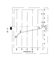
- FIG. 58 is a graph showing the relationship between the chip thickness and the frequency with which the die bond material applied on the wiring board using a multi-point nozzle crawls up to the upper surface of the chip.
- a lead frame was used as the wiring board
- Ag paste was used as the die bond material. From this graph, it can be seen that when the chip thickness is 100 ⁇ m or less, the die bond material creeps up significantly.
- a plurality of electrode pads (bonding pads) made of a conductive material such as Al (aluminum) are exposed from the surface protective film on the upper surface of a chip on which an element such as a MOSFET is formed.
- a plurality of metal wirings that connect between the elements and between the elements and the electrode pads are formed under the surface protective film. For this reason, it has been found that the following problems occur when the die bond material that has risen on the upper surface of the chip adheres to the surface of the electrode pad or the surface protective film covering the metal wiring.
- the die-bonding material runs thick on the surface of the electrode pad, it becomes impossible to connect the bonding wire on the electrode pad in the next wire bonding step.
- the die bond material prevents metal bonding between the bonding wire (initial ball) and the electrode pad, so that non-pressure bonding and insufficient connection strength occur.
- the die bond material is composed of a conductive material such as Ag paste or solder paste
- an electrical short occurs between the adjacent electrode pads via the die bond material.
- the Ag in the Ag paste is caused by thermal stress generated in a baking process for curing the Ag paste or a mold process for resin-sealing the chip.
- the filler may break through the surface protective film (for example, a polyimide resin film having a thickness of about 2 ⁇ m) and short-circuit with the metal wiring under the surface protective film.
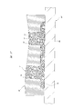
- FIG. 59 schematically shows how the Ag filler in the Ag paste breaks through the surface protective film and short-circuits with the metal wiring.
- the chip 1 is mounted on the metal lead frame LF via the Ag paste 7 is illustrated.
- a metal wiring 36 made of a conductive material such as Al is formed on the uppermost layer of the chip 1, and a surface protective film 19 for protecting the metal wiring 36 is formed thereon.
- the surface protective film 19 is made of, for example, a polyimide resin film having a thickness of about 2 ⁇ m.
- the Ag paste 7 is a conductive die bond material in which an Ag filler 11 having a diameter of about 2 to 15 ⁇ m is dispersed in a base material made of an epoxy resin or the like.
- the Ag paste 7 that has risen on the upper surface of the chip 1 adheres to the surface protective film 19 that covers the metal wiring 36
- a subsequent heat treatment process a baking process for curing the Ag paste 7 or the chip 1 is resin-sealed.
- the Ag filler 11 having a diameter larger than the film thickness of the surface protective film 19 is used as the surface protective film 19. It breaks through and comes into contact with the metal wiring 36. As a result, the metal wiring 36 and the lead frame LF are short-circuited via the Ag paste 7.
- a gate electrode pad connected to the gate electrode of the power MOSFET and a source electrode pad connected to the source are formed on the upper surface of the chip 1.
- a drain electrode is formed on the back surface of the chip 1. Therefore, when the Ag paste 7 climbs up to the upper surface of the chip 1, the drain electrode on the back surface of the chip 1 and the gate electrode pad or the source electrode pad on the main surface of the chip 1 may be short-circuited via the Ag paste 7. is there.
- the base material of Ag paste or insulating paste is mainly composed of an epoxy resin, and when this resin is present in the vicinity of the electrode pad, ionic components (Na + , Cl in the paste during the bias test). - ) And the like are liable to move and cause a leak failure of the ⁇ A order.
- the die bond material may adhere to the lower surface of a collet (bonding nozzle) that adsorbs and holds chips during die bonding, and may contaminate the upper surfaces of other chips that are adsorbed and held next.
- a collet bonding nozzle
- the die bond material that attracts and holds only the center part of the chip with a collet whose diameter is smaller than the outer diameter of the chip and crawls up to the peripheral part of the upper surface of the chip.
- the peripheral portion of the upper surface of the chip does not contact the lower surface of the collet.
- the peripheral portion of the chip is upward.
- the reason why the peripheral portion of the chip warps upward is that the shrinkage rate of the surface protective film is larger than that of the base silicon).
- the peripheral portion of the chip and the die bond material are not in contact with each other, and the contact area between the chip and the die bond material is reduced. Therefore, the chip is easily peeled off from the wiring board due to thermal stress applied in the subsequent heat treatment process. Further, in the case of a chip on which a power MOSFET is formed, an ON resistance is increased.
- a predetermined amount (thickness) of the die bond material is supplied using a printing mask (metal mask or the like).
- a printing mask metal mask or the like.
- the printing range is widened, and the thickness variation of the die bond material at the central portion and the end portion of the wafer becomes large. It is difficult to print stably.
- Ag paste often has an appropriate viscosity by adding a solvent.
- the solvent volatilizes, the volume of the base material (epoxy resin) shrinks, and the Ag fillers in the paste become more closely adhered (mechanically entangled). The electric resistance value is reduced.
- the solvent-type Ag paste having such characteristics is very effective in reducing the ON resistance in a chip on which a power transistor such as a power MOSFET is formed.
- An object of the present invention is to provide a die bonding material coating technique capable of dealing with a thinned chip in manufacturing a semiconductor device including a step of mounting a chip on a wiring board using a paste-like die bonding material. .
- Another object of the present invention is to provide a die bonding material coating technique capable of suppressing excessive wetting and spreading in the manufacture of a semiconductor device having a step of mounting a chip on a wiring board using a paste-like die bonding material. There is.
- a manufacturing method of a semiconductor device which is one embodiment of the present invention is: (A) preparing a wiring board having a chip mounting portion and a plurality of lead terminals arranged adjacent to the chip mounting portion, and a semiconductor chip having a plurality of electrode pads and wiring formed on the main surface; (B) applying a die bond material on the upper surface of the chip mounting portion of the wiring board; (C) mounting the semiconductor chip on the upper surface of the chip mounting portion via the die bond material so that the upper surface of the chip mounting portion and the main surface of the semiconductor chip face the same direction; (D) electrically connecting the plurality of electrode pads of the semiconductor chip and each of the plurality of lead terminals of the wiring board with a conductive material; (E) forming a sealing body that seals the semiconductor chip and the conductive material, and the thickness of the semiconductor chip is less than half the thickness of the chip mounting portion.
- the die bonding material is filled in the digging portion of the nozzle having the digging portion, and the die bonding material filled in the digging portion is used as the upper surface of the chip mounting portion of the wiring board. Further, the transfer is performed so that the coating thickness is thinner than the thickness of the semiconductor chip.
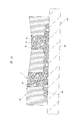
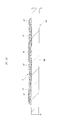
- FIG. 5 is a cross-sectional view taken along line AA in FIG. 4.
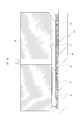
- FIG. 5 is a cross-sectional view taken along line BB in FIG. 4. It is the figure which showed typically the cross-sectional structure of Ag paste interposed between the back surface of the chip
- FIG. 1 is an overall flowchart showing a method for manufacturing a semiconductor device according to a first embodiment of the present invention.
- FIG. 1 is a plan view of a lead frame used for manufacturing a semiconductor device according to a first embodiment of the present invention. It is the schematic which shows the principal part of the paste coating device used for manufacture of the semiconductor device which is Embodiment 1 of this invention.
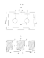
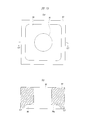
- (A) is the top view which looked at the stamping nozzle with which the front-end
- (b) is sectional drawing along the C1-C1 line of (a).
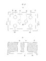
- A) is a plan view showing another example of the stamping nozzle, and (b) is a sectional view taken along line C2-C2 of (a).
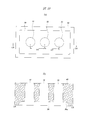
- (A) is a plan view showing another example of the stamping nozzle, and (b) is a cross-sectional view taken along line C3-C3 of (a).
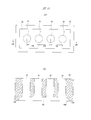
- (A) is a plan view showing another example of the stamping nozzle, and (b) is a cross-sectional view taken along line C4-C4 of (a).
- (A) is a plan view showing another example of the stamping nozzle, and (b) is a cross-sectional view taken along line C5-C5 in (a).
- (A) is a plan view showing another example of the stamping nozzle, and (b) is a cross-sectional view taken along line C6-C6 of (a). It is a top view which shows another example of the planar shape of a chip
- (A) is a plan view showing another example of the stamping nozzle, and (b) is a cross-sectional view taken along line C7-C7 in (a).
- (A) is a plan view showing another example of the stamping nozzle, and (b) is a cross-sectional view taken along line C8-C8 in (a).
- (A) is a plan view showing another example of the stamping nozzle, and (b) is a sectional view taken along line C9-C9 in (a).
- FIG. 29 is a cross-sectional view showing an Ag paste application method following FIG. 28. It is a top view of the lead frame by which Ag paste was apply
- FIG. 31 is a cross-sectional view taken along the line DD in FIG. 30. It is sectional drawing which shows the state which adsorbed and hold
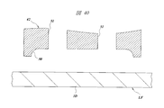
- FIG. 41 is a cross-sectional view showing a solder paste application method following FIG. 40.
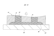
- FIG. 42 is a cross-sectional view showing a solder paste application method following FIG. 41.
- FIG. 43 is a cross-sectional view showing a solder paste application method following FIG. 42. It is sectional drawing which shows the state which adsorbed and hold
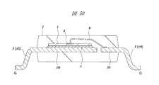
- FIG. 49 is a cross-sectional view taken along line FF in FIG. 48.
- FIG. 49 is a cross-sectional view taken along line GG in FIG. 48.
- FIG. 54 is an enlarged cross-sectional view of a die pad portion shown in FIG. 53 and a chip mounted on the upper surface thereof.
- (A) is a plan view and a sectional view showing an example of a conventional BGA type semiconductor device
- (b) is a plan view and a sectional view showing an example of a BGA type semiconductor device manufactured by the method of the present invention.
- FIG. 56 is an enlarged cross-sectional view showing a part of the conventional BGA type semiconductor device shown in FIG.
- (A) is a top view which shows an example of the chip
- (b) is sectional drawing of this chip
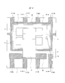
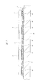
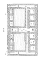
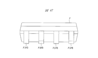
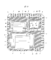
- FIG. 1 is a plan view
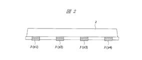
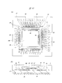
- FIG. 2 is a side view
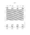
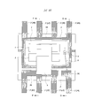
- FIG. 3 is a plan view showing a back surface (substrate mounting surface)
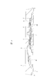
- FIG. 5 is a cross-sectional view taken along the line AA in FIG. 4
- FIG. 6 is a cross-sectional view taken along the line BB in FIG.
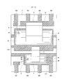
- the semiconductor device of the present embodiment is a small surface mount package (so-called FLP: FlatFLead ⁇ ⁇ Package) in which a chip 1 mounted on a die pad portion (chip mounting portion) 3D of a lead frame is sealed with a mold resin 2.
- Eight leads 3 (# 1 to # 8) constituting external connection terminals of the semiconductor device are exposed on the two side surfaces and the back surface (substrate mounting surface) of the resin 2.
- the die pad portion 3 ⁇ / b> D is exposed together with the eight leads 3 in order to diffuse heat generated in the chip 1 and reduce the thermal resistance of the package.
- the mold resin 2 is made of an insulating material in which a silicon filler is dispersed in, for example, an epoxy resin that is a kind of thermosetting resin.
- the first lead (# 1) to the third lead (# 3) are the source lead
- the fourth lead (# 4) is the gate lead
- the fifth lead is the fifth lead.
- the lead from (# 5) to the eighth lead (# 8) is a drain lead.
- three source leads (# 1 to # 3) are connected to each other inside the mold resin 2.
- the four drain leads (# 5 to # 8) are formed integrally with the die pad portion 3D inside the mold resin 2.
- a portion located within the mold resin 2 (a portion connected to each other) is referred to as a source post 3S, and among the gate leads (# 5), A portion located inside the mold resin 2 is referred to as a gate post 3G.
- the leads 3 (# 1 to # 8) and the die pad portion 3D are made of a metal plate such as Cu (copper), Cu alloy, Fe (iron) -Ni (nickel) alloy, and the thickness thereof is, for example, 200 ⁇ m. .
- the surface of the lead 3 (# 1 to # 8) is plated with a three-layer structure in which a Ni (nickel) film, a Pd (palladium) film, and an Au (gold) film are laminated.
- the chip 1 mounted on the die pad portion 3D is made of single crystal silicon, and has a main surface on which a plurality of power MOSFETs (for example, power control switches and charge / discharge protection circuit switches for portable information devices) are used. (To be described later).
- the back surface of the chip 1 constitutes a common drain for the plurality of power MOSFETs.
- the chip 1 which is an object of the present invention is a chip thinned so that the thickness thereof is 100 ⁇ m or less, and is defined by the relationship with the thickness of the lead frame, the thickness of the die pad portion 3D is one half or less. This is a thin chip having a thickness. Although not particularly limited, a case where the thickness of the chip 1 is 50 ⁇ m and the thickness of the die pad portion 3D is 200 ⁇ m will be described below.
- the main surface of the chip 1 is formed with one gate pad 4 electrically connected to the gate electrode of the power MOSFET and two source pads 5 electrically connected to the source of the power MOSFET. Yes.
- the gate pad 4 is electrically connected to the gate post 3G via the Au wire 8.
- the two source pads 5 are each configured with an area larger than that of the gate pad 5 and an Al (aluminum) ribbon having an area larger than that of the Au wire 8. 9 is electrically connected to the source post 3S.
- the gate pad 4 and the source pad 5 are made of a metal film such as an Al alloy formed on the uppermost layer of the main surface of the chip 1.
- a drain electrode 6 is formed on the back surface of the chip 1 constituting the drain of the power MOSFET.
- the drain electrode 6 is made of, for example, a two-layer metal film in which a Ti (titanium) film having a thickness of 100 nm and an Au film having a thickness of 50 nm are stacked.
- the drain electrode 6 includes a three-layer metal film in which a Ti film having a thickness of 100 nm, a Ni film having a thickness of 200 nm, and an Au film having a thickness of 100 nm are laminated, a Ni film having a thickness of 50 nm, and a Ti film having a thickness of 100 nm.
- the conductive die bond material is Ag paste
- any of these metal films can be used.
- the metal film having the Ni film can form a good alloy with Sn in the solder (solder paste is melted), it is possible to cope with the case where the conductive die bond material is a solder paste.
- an Ag paste 7 which is a kind of conductive die bond material is interposed. That is, the back surface (drain electrode 6) of the chip 1 is bonded to the upper surface of the die pad portion 3D via the Ag paste 7.
- the Ag paste 7 is a conductive die-bonding material in which an Ag filler is dispersed in, for example, an epoxy resin which is a kind of thermosetting resin, and has a feature of extremely high heat dissipation and conductivity. Therefore, the Ag paste 7 is a conductive die bond material suitable for power MOSFETs that require high heat dissipation and low ON resistance.
- space beads are also dispersed together with the Ag filler.
- FIG. 7 is a diagram schematically showing a cross-sectional structure of the Ag paste 7 interposed between the back surface (drain electrode 6) of the chip 1 and the die pad portion 3D.
- Reference numeral 11 in the drawing is an Ag filler, reference numeral 12 Indicates spacer beads, respectively.
- the Ag paste 7 is a so-called solvent-type die bond material to which a solvent is added to give an appropriate viscosity.
- the solvent-type Ag paste 7 is a solvent-free type because the solvent volatilizes during baking and the volume of the base material (epoxy resin) shrinks, and the Ag fillers 11 dispersed in the base material aggregate more densely. It has the characteristic that a low electrical resistance value can be obtained compared with the Ag paste. Therefore, by using the solvent-type Ag paste 7 as a die bond material for bonding the chip 1 on which the power MOSFET is formed to the die pad portion 3D, the power MOSFET is turned on compared to the case where the solvent-free Ag paste is used. Resistance can be reduced.
- the content of the Ag filler 11 in the Ag paste 7 used in the present embodiment is, for example, about 85% before curing and about 95% after curing (after solvent volatilization).
- the size of the Ag filler 11 is, for example, about 2 to 15 ⁇ m.
- the spacer beads 12 included in the Ag paste 7 are, for example, spheres having a diameter of about 15 ⁇ m made of a low elastic epoxy resin, and the content in the Ag paste 7 is, for example, about 15 pieces / mm 2 .
- the spacer beads 12 are added to control the film thickness of the Ag paste 7 interposed between the chip 1 and the die pad portion 3D. That is, by dispersing the spacer beads 12 in the Ag paste 7, the cured Ag paste 7 has a film thickness that is at least about the same as the diameter of the spacer beads 12, even if the film thickness decreases due to the volatilization of the solvent. Thickness is secured.
- the spacer beads 12 made of a low elastic material also have a function of relieving thermal and mechanical stress generated between the chip 1 and the die pad portion 3D.
- a power MOSFET that operates with high power generates a large amount of heat
- a large thermal stress due to a difference in thermal expansion coefficient between the chip 1 and the die pad portion 3D is applied.
- the source pad 5 and the source post 3S are electrically connected using an Al ribbon 9 having a larger area than the Au wire 8
- a large ultrasonic vibration is generated between the chip 1 and the die pad portion 3D during ribbon bonding. Energy is added. Therefore, by adding the spacer beads 12 that are a low elastic material to the Ag paste 7, the above-described thermal and mechanical stresses are absorbed and relaxed by the spacer beads 12, and the separation of the chip 1 and the die pad portion 3D is suppressed.
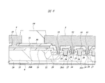
- FIG. 8 is a cross-sectional view of the main part showing the structure of the trench gate type n-channel power MOSFET formed in the chip 1.
- an n ⁇ type single crystal silicon layer 21 is formed by an epitaxial growth method.
- the n + type single crystal silicon substrate 20 and the n ⁇ type single crystal silicon layer 21 constitute the drain of the power MOSFET.
- a p-type well 22 is formed in a part of the n ⁇ -type single crystal silicon layer 21.
- a silicon oxide film 23 is formed on a part of the surface of the n ⁇ -type single crystal silicon layer 21, and a plurality of grooves 24 are formed on the other part.
- a region covered with the silicon oxide film 23 constitutes an element isolation region, and a region where the groove 24 is formed constitutes an element formation region (active region).
- the planar shape of the groove 24 is a polygon such as a quadrangle, a hexagon, or an octagon, or a stripe extending in one direction.
- a silicon oxide film 25 constituting a gate oxide film of the power MOSFET is formed on the bottom and side walls of the trench 24. Further, in the trench 24, a polycrystalline silicon film 26A constituting a gate electrode of the power MOSFET is buried. On the other hand, on the silicon oxide film 23, a gate lead electrode 26B made of a polycrystalline silicon film deposited in the same process as the polycrystalline silicon film 26A constituting the gate electrode is formed. The gate electrode (polycrystalline silicon film 26A) and the gate lead electrode 26B are electrically connected in a region not shown.
- a p ⁇ type semiconductor region 27 shallower than the trench 24 is formed in the n ⁇ type single crystal silicon layer 21 in the element formation region.
- This p ⁇ type semiconductor region 27 constitutes a channel layer of the power MOSFET.
- p - type in the upper part of the semiconductor region 27, p - type semiconductor regions 27 are formed high impurity concentration p-type semiconductor region 28 is more and more the upper portion of the p-type semiconductor region 28, n + -type semiconductor region 29 Is formed.
- the p-type semiconductor region 28 constitutes a punch-through stopper layer of the power MOSFET, and the n + -type semiconductor region 29 constitutes a source.
- Two layers of silicon oxide films 30 and 31 are formed above the element formation region where the power MOSFET is formed and above the element isolation region where the gate lead electrode 26B is formed.
- a connection hole 32 that penetrates through the silicon oxide films 31 and 30, the p-type semiconductor region 28 and the n + -type semiconductor region 29 and reaches the p ⁇ -type semiconductor region 27 is formed.
- a connection hole 33 that penetrates the silicon oxide films 31 and 30 and reaches the gate lead electrode 26B is formed.
- the gate pad 4 and the source pad 5 described above are formed on the silicon oxide film 31 including the insides of the connection holes 32 and 33.
- the gate pad 4 and the source pad 5 are made of a laminated metal film of, for example, a thin TiW (titanium tungsten) film and a thick Al alloy film.
- the source pad 5 formed in the element formation region is electrically connected to the source (n + type semiconductor region 29) of the power MOSFET through the connection hole 32.
- a p + type semiconductor region 34 for making ohmic contact between the source pad 7 and the p ⁇ type semiconductor region 27 is formed at the bottom of the connection hole 32.
- the gate pad 4 formed in the element isolation region is connected to the gate electrode (polycrystalline silicon film 26A) of the power MOSFET via the gate lead electrode 26B below the connection hole 33.
- the outermost surface of the chip 1 is covered with a surface protective film 19 except for the region where the gate pad 4 and the source pad 5 are formed.
- the surface protective film 19 is made of, for example, a polyimide resin film having a thickness of about 2 ⁇ m.
- the drain electrode 6 described above is formed on the back surface of the chip 1, that is, on the back surface of the n + type single crystal silicon substrate 20.
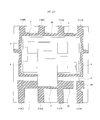
- FIG. 9A is a plan view showing a layout of the gate pad 4 and the source pad 5 formed on the main surface of the chip 1.
- a gate extraction electrode 10 is formed on the periphery and center of the main surface of the chip 1.
- One end of the gate lead electrode 10 formed at the center of the main surface of the chip 1 constitutes a gate pad 4.
- a pair of source pads 5 are formed on both sides of the gate extraction electrode 10 formed at the center of the main surface of the chip 1.
- the gate extraction electrode 10, the gate pad 4 and the source pad 5 are made of a metal film such as an Al alloy formed on the uppermost layer of the main surface of the chip 1.
- the gate extraction electrode 10 is covered with the surface protective film 19. ing.
- each gate electrode (polycrystalline silicon film 26A) of the power MOSFET shown in FIG. It extends linearly toward 10 and is electrically connected to the gate extraction electrode 10.
- the length of the gate electrode (polycrystalline silicon film 26A) can be made substantially uniform over the entire main surface of the chip 1, the switching characteristics of the power MOSFET are improved.
- the gate pad 4 may be disposed at a corner portion of the main surface of the chip 1 as shown in FIG. In this way, the length of the Au wire 8 connecting the gate pad 4 and the gate post 3G can be shortened as compared to the layout shown in FIG. 9A (see FIGS. 4 and 10).
- the source pad 5 is not limited to the layout shown in FIG.
- the gate extraction electrode 10 may be disposed only on the outer peripheral portion of the main surface of the chip 1, and one source pad 5 may be disposed in the center portion. In this way, the area of the source pad 5 can be increased, so that the ON resistance of the power MOSFET can be further reduced.
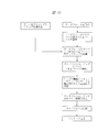
- FIG. 12 is an overall flowchart showing a method for manufacturing a small surface-mount package according to the present embodiment.
- the above-described power MOSFET is formed on the main surface of the semiconductor wafer 1A shown in FIG. 13 by using a semiconductor wafer manufacturing process, and then the back surface of the semiconductor wafer 1A is ground to obtain the semiconductor wafer.
- the thickness of 1A is reduced to 50 ⁇ m here.
- the semiconductor wafer 1A is diced to obtain a plurality of chips 1.
- the lead frame LF has a structure in which the lead 3 (# 1 to # 8) and the die pad portion 3D described above are supported by a rectangular frame 13, and the thickness thereof is 200 ⁇ m here.
- the fourth lead (# 4) constituting the gate lead and the first lead (# 1) to third lead (# 3) constituting the source lead are bent into a predetermined shape (FIG. 5, FIG. 5). (See FIG. 6).
- the actual lead frame has a structure in which a large number of die pad portions 3D are arranged in a matrix inside the frame 13, but here, in order to make the drawing easier to see, the two lead pad portions 3D are provided.
- the lead frame LF will be described as an example.
- the aforementioned Ag paste 7 is applied on the die pad portion 3D of the lead frame LF.
- a stamping method described in detail below is employed as a method of applying the Ag paste 7 on the die pad portion 3D.
- FIG. 15 is a schematic view showing the main part of the paste application device 40.
- the paste application device 40 includes a syringe 41 filled with an uncured Ag paste 7 and a stamping nozzle 42 attached to the tip (lower end) of the syringe 41.
- the syringe 41 is supported by an arm 44 attached to the drive unit 43, and is moved in the horizontal direction (XY direction) and the vertical direction (Z direction) by a motor built in the drive unit 43. .
- the syringe 41 is supplied with a predetermined amount of air from an air supply source (not shown) through a pipe 45 connected to the upper end portion thereof. Also, a piston 46 is inserted inside the syringe 41, and the piston 46 descends due to the pressure of the air supplied to the inside of the syringe 41, so that a predetermined amount of Ag paste 7 corresponding to the air supply amount is formed. It is transferred from the syringe 41 to the stamping nozzle 42.
- FIG. 16A is a plan view of the stamping nozzle 42 attached to the distal end portion of the syringe 41 as seen from the lower surface side, and FIG. 16B is along the line C1-C1 in FIG. FIG.
- the stamping nozzle 42 is made of a corrosion-resistant metal such as stainless steel, and the planar shape of the lower surface thereof is rectangular. On the lower surface of the stamping nozzle 42, a digging portion (holding portion, reservoir portion, space portion) 50 serving as a space filled with the Ag paste 7 is provided. The stamping nozzle 42 is attached to the syringe 41 such that the center of the digging portion 50 coincides with the center of the distal end portion (Ag paste discharge portion) of the syringe 41.
- the planar shape of the dug portion 50 is a rectangle, and the ratio of the long side length to the short side length is substantially the same as the ratio of the long side length to the short side length of the chip 1. Further, the planar dimension of the dug portion 50 is formed to be smaller by about 100 to 500 ⁇ m on one side than the outer dimension of the chip 1. Further, the thickness (t) from the outer edge of the dug portion 50 to the side surface of the stamping nozzle 42 is preferably 200 to 500 ⁇ m. If the thickness (t) is secured to this level, the life of the stamping nozzle 42 is hardly affected. Furthermore, by setting the outer dimension of the lower surface of the stamping nozzle 42 to be approximately the outer dimension of the chip 1 + 100 ⁇ m on one side, the possibility that the stamping nozzle 42 interferes with the surrounding area during work can be reduced.
- the digging portion 50 has a digging surface 50a located above the lower surface of the stamping nozzle 42, and four side walls 50b surrounding the digging surface 50a.
- the digging surface 50a and the side wall 50b have a smooth mirror finish without any irregularities.
- intersect is R shape.
- the releasability with respect to the inner wall (digging surface 50a and side wall 50b) of the digging part 50 of Ag paste 7 improves, and Ag paste 7 adheres to the inner wall of the digging part 50, or in Ag paste 7 Since the problem that the Ag filler 11 and the spacer beads 12 remain in the digging portion 50 is improved, it is possible to reduce variation in the coating amount of the Ag paste 7 transferred onto the die pad portion 3D.
- a pair of flow paths 51 for sending the Ag paste 7 in the syringe 41 to the digging portion 50 are provided above the digging portion 50.
- the lower ends of these flow paths 51 are located on the digging surface 50a. Accordingly, when the digging surface 51a is viewed from the lower surface side of the stamping nozzle 42, the flow path 51 appears as an opening.
- the two flow paths (openings) 51 provided in the stamping nozzle 42 are positioned equidistant from the center of the digging portion 50 along the long side direction and on a line connecting the centers of the two short sides. Has been placed.
- the pitch (P1) of the two flow paths 51 is preferably set to about one third to one half of the length of the long side of the dug portion 50.
- the number of flow paths 51 provided in the stamping nozzle 42 is not limited to two, and may be optimized as appropriate according to the external dimensions of the chip 1 and the ratio of the length of the long side to the length of the short side. desirable.
- the number of the flow paths 51 may be one.
- the problem that the filling amount of the Ag paste 7 is insufficient in the vicinity of the corner portion of the digging portion 50 is improved by providing three or more flow paths 51 in the stamping nozzle 42. can do.
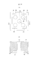
- FIG. 17 shows an example in which five flow paths 51 are provided in the stamping nozzle 42.
- One channel 51a is arranged at the center of the digging portion 50, and the remaining four channels 51b are arranged so as to surround the channel 51a and are arranged in the vicinity of the corner portion of the digging portion 50.
- the pitch (P2) between the channel 51a arranged at the center of the digging portion 50 and the channel 51b arranged around it is set to about one third to one half of the length of the diagonal line. Is preferred.
- the stamping nozzle 42 shown in FIG. 17 can stabilize the filling amount of the Ag paste 7 at the corner portion because the flow path 51b is disposed in the vicinity of the corner portion of the digging portion 50.
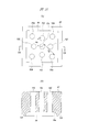
- FIG. 18 shows an example in which six flow paths 51 are provided in the stamping nozzle 42.
- the two flow paths 51c arranged in the vicinity of the center of the digging portion 50 are arranged at equidistant positions along the long side direction from the center of the digging portion 50, and the digging portion 50. It is arranged on the center line of the short side.
- the pitch of the two flow paths 51c (P3) is preferably not more than a quarter of the length of the long side of the digging portion 50.
- the four flow paths 51d are arranged on a diagonal line connecting the corner portions of the digging portion 50, and the distances from the center of the digging portion 50 to the respective flow paths 51d are the same.
- the distance from the center of the digging part 50 to each flow path 51c is one quarter or more of the length of the diagonal line.
- the stamping nozzle 42 shown in FIG. 18 is formed on the center line of the short side of the digging portion 50 even if the tip 1 has a long and narrow shape and the digging portion 50 has a long and narrow shape. Since the two flow paths 51c are arranged, the digging portion 50 can be stably filled with the Ag paste 7 as compared with the stamping nozzle 42 shown in FIG.
- FIG. 19 shows an example in which nine flow paths 51 are provided in the stamping nozzle 42.
- the centers of the nine flow paths 51 coincide with the center of the digging portion 50, and one flow path 51 e is arranged there.
- the two flow paths 51f are arranged on a line connecting the center of one long side of the digging portion 50 and the center of the other long side, and the two flow paths 51g are formed in the digging portion 50.
- the remaining four flow paths 51 h are arranged on a diagonal line connecting the corner portions of the dug portion 50.
- the pitch (P4) between the flow path 51e and the flow path 51f be equal to or less than a quarter of the length of the short side of the digging portion 50.
- the pitch (P5) of the flow path 51e and the flow path 51g be set to 1 ⁇ 4 or less of the length of the long side of the digging portion 50.
- the pitch (P6) of the flow path 51e and the flow path 51h is not less than 1 ⁇ 4 of the length of the diagonal line.
- the stamping nozzle 42 shown in FIG. 19 has, for example, two flow paths 51f on a line connecting the center of one long side of the digging portion 50 and the center of the other long side even when the outer dimensions of the chip 1 are increased. Since two flow paths 51g are arranged on a line connecting the center of one short side and the center of the other short side, and four flow paths 51h are arranged on a diagonal line connecting the corner portions, FIG. Compared to the stamping nozzle 42 shown in FIG. 2, the Ag paste 7 can be stably filled in the digging portion 50.
- FIG. 20 is an example in which three flow paths 51 are provided in a row along the long side direction of the dug portion 50, and FIG. 21 shows four channels 51 along the long side direction of the dug portion 50. This is an example in which the flow paths 51 are provided in a line. These examples are structures suitable when the ratio of the long side length to the short side length of the chip 1 is large.
- the three flow paths 51 are arranged on a line connecting the center of one short side of the digging portion 50 and the center of the other short side, and the central flow path 51 is It is arranged at the center of the dug portion 50. Moreover, it is preferable that the pitch (P7) of the adjacent flow paths 51 is set to about one third of the length of the long side of the digging portion 50.
- the four flow paths 51 are arranged on a line connecting the center of one short side of the digging portion 50 and the center of the other short side, and the centers of the four flow paths 51 are digged. It coincides with the center of the part 50. Moreover, it is preferable that the pitch (P8) of the adjacent flow paths 51 is set to about a quarter of the length of the long side of the digging portion 50.
- the stamping nozzle 42 shown in FIGS. 16 to 21 is used when the planar shape of the chip 1 is a rectangle, but when the planar shape of the chip 1 is a square as shown in FIG. It is desirable to use a stamping nozzle 42 in which the dug portion 50 has a square planar shape.
- FIG. 23 is an example in which one flow path 51 is provided in the stamping nozzle 42 in which the planar shape of the dug portion 50 is a square.
- FIG. 24 shows an example in which five flow paths 51 are provided in a stamping nozzle 42 in which the planar shape of the dug portion 50 is a square.
- the five flow paths 51 are arranged on a diagonal line connecting the corner portions of the digging portion 50, and their centers coincide with the center of the digging portion 50. Yes.
- the pitch (P2) between the flow path 51a disposed at the center of the digging portion 50 and the flow path 51b around it is set to about one third to one half of the length of the diagonal line. preferable.
- the stamping nozzle 42 shown in FIG. 24 is similar to the example shown in FIG. 17 in that the channel 51b is disposed in the vicinity of the corner portion of the dug portion 50, and therefore, the corner portion is smaller than the stamping nozzle 42 shown in FIG.
- the amount of the Ag paste 7 filled can be stabilized.
- FIG. 25 shows an example in which nine flow paths 51 are provided in a stamping nozzle 42 in which the planar shape of the dug portion 50 is a square.
- the centers of the nine flow paths 51 coincide with the center of the digging portion 50, and one flow path 51 e is arranged there.
- the four flow paths 51 f are arranged on a line connecting the center of the digging portion 50 and the center of one side, and the remaining four flow paths 51 h are diagonal lines connecting the corner portions of the digging portion 50. Is placed on top.
- the pitch (P4) between the flow path 51e and the flow path 51f is preferably about one-sixth to one-fourth of the length of one side of the digging portion 50, and the pitch between the flow path 51e and the flow path 51h ( P6) is preferably not less than the above pitch (P4) ⁇ ⁇ 2.
- the stamping nozzle 42 shown in FIG. 25 includes, for example, four flow paths 51f on the line connecting the center of the digging portion 50 and the center of one side and the corner portion of the digging portion 50 even when the outer dimensions of the chip 1 are increased. Since the four flow paths 51h are arranged on the diagonal line connecting each other, it is possible to stably fill the digging portion 50 with the Ag paste 7 as compared with the stamping nozzle 42 shown in FIG.
- the planar shape of the flow path 51 is circular, but may be rectangular. In any case, it is preferable that the opening diameter of the flow path 51 is set to such an extent that the Ag paste 7 does not sag during standby and is not clogged by the Ag filler 11 or the spacer beads 12. Further, the number of the flow paths 51 is not limited to the examples shown in FIGS. Further, the planar dimensions and depth (D) of the digging portion 50, the wall thickness (t) from the side wall of the digging portion 50 to the side surface of the stamping nozzle 42, and the like are the same specifications as the stamping nozzle 42 shown in FIG. It is desirable to make it.
- the Ag paste 7 filled in the syringe 41 of the paste application device 40 is dug by the stamping nozzle 42.
- the lower surface of the stamping nozzle 42 is abutted against the upper surface of the die pad portion 3D.
- the Ag paste 7 filled in the digging portion 50 is detached from the digging portion 50 and transferred onto the die pad portion 3D. That is, an amount of Ag paste 7 corresponding to the volume of the dug portion 50 is transferred onto the die pad portion 3D.
- the shape of the Ag paste 7 transferred onto the die pad portion 3D is substantially the same as the shape of the digging portion 50.
- the thickness of the Ag paste 7 applied on the die pad portion 3 ⁇ / b> D is smaller than the thickness of the chip 1 ( getting thin.
- the planar dimension of the dug portion 50 is smaller than the outer dimension of the chip 1
- the outer dimension of the Ag paste 7 applied on the die pad portion 3 ⁇ / b> D is smaller than the outer dimension of the chip 1.
- the air in the dug portion 50 is more easily discharged in the second method than in the first method. That is, in the second method, as shown in FIG. 28, the lower end of the Ag paste 7 discharged from the flow path 51 into the digging portion 50 is protruded downward from the lower surface of the stamping nozzle 42.
- the Ag paste 7 can be filled into the digging portion 50 without any gaps while escaping (extruding) air in the portion 50. As a result, voids in the Ag paste 7 applied on the die pad portion 3D can be reduced.
- FIG. 30 is a plan view of the lead frame LF in which the Ag paste 7 is applied on the die pad portion 3D by the above-described method
- FIG. 31 is a cross-sectional view taken along the line DD in FIG.
- the main surface of the chip 1 is transported above the die pad portion 3D while being sucked and held by the die bonding collet 54, and the main surface of the chip 1 and the upper surface of the die pad portion 3D are parallel to each other. Position so that
- the outer dimensions of the die bonding collet 54 are preferably larger than the outer dimensions of the chip 1.
- the die bonding collet 54 larger than the outer dimensions of the chip 1 is used, the entire peripheral portion of the main surface of the chip 1 comes into contact with the lower surface of the die bonding collet 54.
- the peripheral portion of the chip 1 does not warp, so that the entire back surface of the chip 1 can be wetted with the Ag paste 7.
- the adhesion between the chip 1 and the Ag paste 7 is ensured, so that the connection reliability between the chip 1 and the die pad portion 3D is improved.
- an increase in the ON resistance of the power MOSFET is suppressed.
- the die bonding collet 54 is vertically lowered, and the back surface of the chip 1 is lightly pressed against the Ag paste 7 on the die pad portion 3D.
- the load (mounting load) applied to the Ag paste 7 is, for example, about 60 to 150 g / chip.
- the Ag paste 7 includes the spherical spacer beads 12 made of a low elastic resin, when the chip 1 is pressed against the Ag paste 7, the Ag paste 7 wets and spreads in the lateral direction, and the film The thickness is reduced to approximately the same as the diameter of the spacer beads 12, and a part of the Ag paste 7 protrudes outside the chip 1.
- the Ag paste 7 is applied on the die pad portion 3D so that its thickness is thinner than the thickness of the chip 1 and its outer dimension is smaller than the outer dimension of the chip 1.
- the paste 7 protrudes slightly and does not adhere to the die bonding collet 54. Further, the Ag paste 7 does not crawl on the main surface (upper surface) of the chip 1 after the die bonding collet 54 is separated from the chip 1.
- the upper end portion of the fillet of the Ag paste 7 formed around the chip 1 is located between the main surface (upper surface) and the rear surface (lower surface) of the chip 1.
- the upper end portion of the fillet of the Ag paste 7 is located between the main surface (upper surface) of the chip 1 and the aforementioned metal film formed on the rear surface (lower surface) of the chip 1.
- the volume of the digging portion 50 of the stamping nozzle 42 (that is, the volume of the Ag paste 7 applied on the die pad portion 3D) is the same as the position of the upper end of the fillet of the Ag paste 7 described above. Means that it is important to set the
- the drain electrode 6 formed on the back surface of the chip 1 and the gate pad 4 or the source pad 5 formed on the main surface of the chip 1 are short-circuited via the Ag paste 7 is prevented. be able to.
- the Ag filler 11 in the Ag paste 7 breaks through the surface protective film 19 covering the main surface of the chip 1 and comes into contact with the gate extraction electrode 10, and the drain electrode 6 and the gate extraction electrode 10 are short-circuited through the Ag paste 7. It is possible to prevent such problems.
- FIG. 34 is a plan view showing the lead frame LF immediately after the die bonding collet 54 is separated from the chip 1 after pressing the back surface of the chip 1 against the Ag paste 7 using the die bonding collet 54.
- FIG. FIG. 6 is an enlarged plan view showing a part of (a rectangular region indicated by reference numeral E).
- the amount of protrusion (a) of the Ag paste 7 at the corner portion of the chip 1 is separated from the corner portion.
- the relationship with the protruding amount (b) of the Ag paste 7 in the region is (b / a) ⁇ 2.
- the amount of protrusion (a) means the amount of protrusion from the corner portion of the chip 1 in an oblique 45 ° direction
- the amount of protrusion (b) is the amount of protrusion from one side of the chip 1 in the direction perpendicular to the side. Means.
- the amount of protrusion (b) in the region away from the corner portion of the chip 1 is the amount of protrusion (a) in the corner portion of the chip 1 (a ) Less than twice. Therefore, even if the thickness of the chip 1 is 100 ⁇ m or less, a part of the Ag paste 7 that protrudes outside the chip 1 does not crawl up to the upper surface (main surface) of the chip 1.
- FIG. 36 shows the amount of protrusion of the Ag paste 7 when the back surface of the chip 1 is pressed against the Ag paste 7 after applying the Ag paste 7 on the die pad portion 3D using the conventional multipoint nozzle method.
- the relationship between the protrusion amount (a) of the Ag paste 7 at the corner portion of the chip 1 and the protrusion amount (b) of the Ag paste 7 in the region away from the corner portion of the chip 1 is (b / a)> 2 That is, the protruding amount (b) of the Ag paste 7 in the region away from the corner portion of the chip 1 is larger than twice the protruding amount (a) of the Ag paste 7 in the corner portion of the chip 1. Therefore, when the thickness of the chip 1 is 100 ⁇ m or less, a part of the Ag paste 7 that protrudes to the outside of the chip 1 crawls up to the upper surface (main surface) of the chip 1.
- the gate pad 4 of the chip 1 and the gate post 3G of the lead frame LF are connected as shown in FIG.
- the Au wire 8 is electrically connected, and the source pad 5 of the chip 1 and the source post 3S of the lead frame LF are electrically connected by the Al ribbon 9.
- a ball bonding method using both heat and ultrasonic vibration is used, and for bonding the Al ribbon 9, a wedge bonding method using ultrasonic vibration is used.
- the bonding order of the Au wire 8 and the Al ribbon 9 is arbitrary. However, since the width and thickness of the Al ribbon 9 are larger than the diameter of the Au wire 8, the vibration energy applied to the chip 1 during bonding of the Al ribbon 9 is greater than the vibration energy applied to the chip 1 during bonding of the Au wire 8. large. Therefore, when the Al ribbon 9 is bonded after the Au wire 8 is bonded, the connection strength between the Au wire 8 and the gate pad 4 is reduced due to vibration energy at the time of bonding of the Al ribbon 9. The gate pad 4 may be peeled off. Further, when the wedge tool used for bonding the Al ribbon 9 contacts the Au wire 8, the Au wire 8 may be damaged or cut. Therefore, it is desirable to bond the Al ribbon 9 first and then bond the Au wire 8 after that.
- the conductive material for connecting the source pad 5 and the source post 3S is not limited to the Al ribbon 9, and for example, as shown in FIG. 38, a plurality of Au wires 8 are used to form the source pad 5 and the source post. 3S may be connected. At this time, long Au wires 8 and short Au wires 8 are alternately arranged and connected (staggered arrangement) to efficiently connect between the source pads 5 and the source posts 3S with a plurality of Au wires 8. can do.
- a metal clip that is a conductive material similar to the Al ribbon 9 can also be used.
- the clip is a thin metal plate made of Cu alloy, Al, or the like, formed in advance in a predetermined loop shape and a predetermined length, with one end on the source pad 5 and the other end on the source post 3S.
- connection methods include solder bonding, Ag paste bonding, and ultrasonic bonding.
- the chip 1 is sealed with the mold resin 2. Thereafter, by cutting and removing the frame 13 of the lead frame LF exposed to the outside of the mold resin 2, the semiconductor device (small surface mount package) of the present embodiment shown in FIGS. 1 to 5 is completed.
- the manufacturing method of the present embodiment described above when the thin chip 1 having a thickness of 100 ⁇ m or less is mounted on the die pad portion 3D of the lead frame LF, the upper surface of the chip 1 where the Ag paste 7 is thin. It is possible to improve the problem of creeping. As a result, the thinning of the chip 1 mounted on the die pad portion 3D can be promoted, so that the small surface mount package for sealing the chip 1 on which the power MOSFET is formed and the high performance (power MOSFET) Low ON resistance).
- the present invention the case where the Ag paste 7 is used as the die bonding material for connecting the die pad portion 3D of the lead frame LF and the chip 1 has been described.
- the method of applying the die bonding material using the stamping nozzle 42 described above is as follows.
- the present invention can also be applied when a solder paste (solder paste) is used as the die bond material.
- the solder paste is a conductive die-bonding material in which a flux mainly composed of rosin and solder fine particles are kneaded.
- the solder component includes Sn (tin) -Pb (lead) alloy and Sn containing no Pb. -Ag-Cu alloy, Sn-Zn (zinc) -Bi (bismuth) alloy, Sn-Ag-In (indium) -Bi alloy, and the like. Since the solder paste has lower conductivity but higher heat resistance than the Ag paste 7, a semiconductor device used in a high temperature environment such as a semiconductor package for sealing the chip 1 on which the in-vehicle power MOSFET is formed, for example. It is a die-bonding material suitable for use in.
- the stamping nozzle 42 is positioned above the die pad portion 3D.
- the stamping nozzle 42 is attached to the tip of the syringe 41 of the paste applying device 40 (see FIG. 15) described above, and the inside of the syringe 41 is filled with solder paste.
- the number and layout of the flow paths 51 provided in the stamping nozzle 42 are optimized as appropriate according to the external dimensions of the chip 1 and the ratio of the length of the long side to the length of the short side.
- a stamping nozzle 42 is used.
- the planar shape of the chip 1 is a rectangle
- the planar shape of the digging portion 50 is also a rectangle
- the ratio of the length of the long side to the length of the short side is the length of the long side of the chip 1. Is almost the same as the ratio of the length of the short side.
- the planar dimension and depth of the dug portion 50 are smaller than the planar dimension and thickness of the chip 1. For example, when the thickness of the chip 1 is 50 ⁇ m, the depth of the dug portion 50 is set to 30 to 40 ⁇ m.
- the solder paste 14 is discharged into the digging portion 50 through the flow path 51.
- the lower end of the solder paste 14 discharged into the digging portion 50 is projected downward from the lower surface of the stamping nozzle 42.
- the solder paste 14 is filled in the digging portion 50 without any gaps while releasing the air in the digging portion 50. can do.
- the lower surface of the stamping nozzle 42 is brought into contact with the upper surface of the die pad portion 3D to fill the digging portion 50 with the solder paste 14, and then the stamping nozzle 42 is moved as shown in FIG. By pulling up, the solder paste 14 in the digging portion 50 is transferred onto the die pad portion 3D.
- the inner wall of the digging portion 50 is mirror-finished, so that the variation in the application amount of the solder paste 14 transferred onto the die pad portion 3D can be reduced.
- the main surface of the chip 1 is conveyed above the die pad portion 3D while being sucked and held by the die bonding collet 54, and the main surface of the chip 1 and the upper surface of the die pad portion 3D are parallel to each other.
- the back surface of the chip 1 is lightly pressed against the solder paste 14 on the die pad portion 3D, and a load is applied to the solder paste 14.
- the solder paste 14 spreads in the horizontal direction, and a part of the solder paste 14 protrudes from the peripheral portion of the chip 1 to the outside.
- the solder paste 14 applied on the die pad portion 3D is thinner than the thickness of the chip 1 and its outer dimension is smaller than the outer dimension of the chip 1, so that the solder protruding outside the chip 1 is present.
- the paste 14 does not adhere to the die bonding collet 54. Further, after the die bonding collet 54 is separated from the chip 1, the solder paste 14 does not crawl on the main surface (upper surface) of the chip 1.
- the chip 1 is slightly buried in the solder paste 14. That is, the upper surface of the solder paste 14 that protrudes outward from the peripheral portion of the chip 1 is higher than the back surface of the chip 1 in the thickness direction (height direction) of the chip. In other words, the upper surface of the solder paste 14 that protrudes outward from the peripheral portion of the chip 1 is located between the main surface (upper surface) and the rear surface (lower surface) of the chip 1. Alternatively, the upper surface of the solder paste 14 that protrudes outward from the peripheral portion of the chip 1 is located between the main surface (upper surface) of the chip 1 and the aforementioned metal film formed on the rear surface (lower surface) of the chip 1. Yes.
- the solder solidified by melting the solder paste 14 is joined (metal bonded) to the metal film on the back surface of the chip 1, and the upper end of the solidified solder fillet is formed of metal. It does not cross the membrane. This is because the chip 1 is made of silicon, and the solder in which the solder paste 14 is melted has a property of not getting wet with silicon (not forming a metal bond).
- the solder paste 14 applied on the die pad portion 3D is made thicker than the Ag paste 7, and the solder film after reflowing By increasing the thickness, the bonding reliability between the chip 1 and the die pad portion 3D can be further improved.
- the solder paste 14 spreads on the upper surface of the thin chip 1.
- the problem that goes up can be improved. Thereby, even if it is a case where the solder paste 14 is used as a die-bonding material, thickness reduction of the chip
- the small surface mounting package for sealing the chip 1 is not limited to the FLP, and various surface mounting packages can be adopted, for example, SOP8 as shown in FIGS. 46 to 50 is adopted.
- FIG. 47 is a side view of the SOP 8
- FIG. 48 is a plan view showing the internal structure of the SOP 8
- FIG. 49 is a cross-sectional view taken along the line FF in FIG. It is sectional drawing along the GG line.
- the SOP 8 is a surface mount package in which leads 3 (# 1 to # 8) protruding from two side surfaces of the mold resin 2 are formed in a gull wing shape.
- the Ag paste 7 (or solder paste 14) is spread on the upper surface of the thin chip 1 by applying the Ag paste 7 (or solder paste 14) on the die pad portion 3D using the stamping nozzle 42 described above. Since the malfunction which goes up can be improved, thickness reduction of the chip
- the element formed on the chip 1 may be an IGBT (Insulated Gate Bipolar Transistor).
- IGBT Insulated Gate Bipolar Transistor
- the collector electrode is formed on the back surface of the chip 1 on which the IGBT is formed, Ag paste 7 or solder paste 14 is used as a die bonding material when the chip 1 is mounted on the die pad portion 3D. Therefore, also in this case, the problem that the die bond material crawls up to the upper surface of the chip 1 can be improved by applying the die bond material using the stamping nozzle 42 described above.
- FIG. 51 is a plan view showing the internal structure of the semiconductor device of the present embodiment
- FIG. 52 is an internal equivalent circuit diagram of the semiconductor device.
- the semiconductor device according to the present embodiment is a small surface-mount package in which two chips 1H and 1L are sealed with a mold resin 2.
- As the package shape various shapes such as the aforementioned FLP and SOP8 can be adopted.
- a high-side MOSFET is formed on the main surface of the chip 1H having a small outer diameter
- a low-side MOSFET is formed on the main surface of the chip 1L having a large outer diameter.
- Each of the two chips 1H and 1L has a thickness of 100 ⁇ m or less.
- the source of the high-side MOSFET and the drain of the low-side MOSFET are electrically connected to form a DC-DC converter, for example. Since the specific structures of the high-side MOSFET and the low-side MOSFET are substantially the same as those of the power MOSFET of the first embodiment, their illustration is omitted.
- the chip 1H having a small outer diameter is mounted on the die pad portion 3P1 formed integrally with the three drain leads 3D1 with the main surface thereof facing upward. Has been. On the main surface of the chip 1H, one gate pad 4h and two source pads 5h having a larger area than the gate pad 4h are formed.
- the back surface of the chip 1H constitutes the drain of the high-side MOSFET, and is joined to the top surface of the die pad portion 3P1 via the same Ag paste 7 as used in the first embodiment.
- the chip 1L having a large outer diameter is mounted on the die pad portion 3P2 having a larger area than the die pad portion 3P1 with its main surface facing upward.
- On the main surface of the chip 1L one gate pad 41 and two source pads 51 having a larger area than the gate pad 41 are formed.
- the back surface of the chip 1L constitutes the drain of the low-side MOSFET, and is joined to the top surface of the die pad portion 3P2 via the same Ag paste 7 used in the first embodiment.
- one gate lead 3G1 is arranged together with the three drain leads 3D1.
- the gate pad 4h of the chip 1H and the gate lead 3G1 are electrically connected via the Au wire 8
- the source pad 5h of the chip 1H and the die pad portion 3P2 are electrically connected via the Al ribbon 9. Yes.
- three source leads 3S2 and one gate lead 3G2 are arranged on the other side of the mold resin 2, and three source leads 3S2 and one gate lead 3G2 are arranged.
- the three source leads 3S2 are connected to each other inside the mold resin 2, and the connected portion (source post 3S) and the source pad 5l of the chip 1L are electrically connected via the Al ribbon 9. ing.
- the gate lead 3G2 is electrically connected to the gate pad 4l of the chip 1L via the Au wire 8.
- the Ag paste 7 is applied to the upper surfaces of the two die pad portions 3P1 and 3P2 using the stamping nozzle 42 described above. As a result, it is possible to improve the problem of the Ag paste 7 creeping up on the upper surfaces of the thin chips 1H and 1L, so that the thinning of the chips 1H and 1L can be promoted.
- the stamping nozzle 42 for applying the Ag paste 7 on the die pad portion 3P1 and the stamping nozzle 42 for applying the Ag paste 7 on the die pad portion 3P2 are moats.
- the thing in which the planar dimension of the insertion part 50 differs is used.
- solder paste 14 can be used in place of Ag paste 7.
- FIG. 53 shows a system-in-package (SIP) in which the above-described two chips 1H, 1L and a third chip 1D on which a driver IC (or control IC) is formed are sealed with a mold resin 2. It is a top view which shows the internal structure of.
- SIP system-in-package
- the chip 1H on which the high-side MOSFET is formed is bonded to the upper surface of the die pad portion 3P1 via the Ag paste 7, and the chip 1L on which the low-side MOSFET is formed is bonded to the upper surface of the die pad portion 3P2 via the Ag paste 7. ing.
- Each of the two chips 1H and 1L has a thickness of 100 ⁇ m or less. Therefore, even when these chips 1H and 1L are mounted on the die pad portions 3P1 and 3P2, by applying the Ag paste 7 on the die pad portions 3P1 and 3P2 by the stamping method using the stamping nozzle 42 described above, the chip 1H The problem that the Ag paste 7 crawls on the upper surface of 1 L can be improved.
- the insulating paste 15 is an insulating die bond material in which silica is dispersed in a thermosetting resin such as an epoxy resin.
- a plurality of electrode pads (bonding pads) 16 that are electrically connected to elements constituting the driver IC are formed on the periphery of the main surface of the chip 1D. These electrode pads 16 are electrically connected to the gate pads 4h and 4l of the chips 1H and 1L or the leads 3 through Au wires 8. Thus, since the chip 1D on which the driver IC is formed does not need to be electrically connected between the back surface and the die pad portion 3P3, the die pad portion 3P3 is interposed via the insulating paste 15 that is an insulating die bond material. Mounted on top.
- FIG. 54 is an enlarged sectional view of the die pad portion 3P3 and the chip 1D mounted on the upper surface thereof.
- the insulating paste 15 is applied on the die pad portion 3P3, and then the chip 1D is pressed against the insulating paste 15 from above, so that the entire back surface of the chip 1D is applied. After wetting with the insulating paste 15, the insulating paste 15 is thermally cured.
- the chip 1D is applied when the chip 1D is pressed against the insulating paste 15 after applying the insulating paste 15 on the die pad portion 3P3 using a multi-point nozzle or the like.
- a phenomenon occurs in which a part of the insulating paste 15 that protrudes outside the surface crawls up to the upper surface (main surface) of the chip 1D. Since a plurality of electrode pads 16 are formed on the periphery of the main surface of the chip 1D, when the insulating paste 15 crawls on the main surface of the chip 1D, the surface of the electrode pad 16 is covered with the insulating paste 15. Will be covered.
- the electrode pad 16 and the Au wire 8 are not in contact with each other, or the adhesion between the two is greatly reduced.
- the insulating paste 15 is applied to the upper surface of the chip 1D by applying the insulating paste 15 on the die pad portion 3P3 by the stamping method using the stamping nozzle 42 described above.
- the problem of scooping up can be improved.
- the upper end portion of the fillet of the insulating paste 15 formed around the chip 1D is formed between the main surface (upper surface) and the rear surface (lower surface) of the chip 1D as in the case of the Ag paste 7. Located between.
- the volume of the digging portion 50 of the stamping nozzle 42 (that is, the volume of the insulating paste 15 applied on the die pad portion 3D) is the same as the position of the upper end of the fillet of the insulating paste 15 described above. Means that it is important to set the
- the chip 1D on which the driver IC is formed is bonded to the upper surface of the die pad portion 3P3 via the insulating paste 15 has been described.
- the Ag paste 7 may be used instead of the insulating paste 15 . Since no electrode is formed on the back surface of the chip 1D on which the driver IC is formed, even if the Ag paste 7 which is a conductive material is used, an electrical failure does not occur.
- thermosetting treatment can be performed once. This can simplify the number of assembling steps compared to a case where the insulating paste 15 is used for the die bonding material of the chip 1D and the thermosetting treatment is performed twice.
- FIG. 55 shows a BGA type semiconductor device in which a chip 1M on which a multi-pin integrated circuit such as a microcomputer is formed is mounted on a wiring board 17.
- the chip 1C is mounted on the upper surface of the wiring board 17 serving as a relay board (interposer) for connecting the chip 1M to the motherboard of the electronic component via the insulating paste 15 described above.
- a plurality of electrode pads (bonding pads) 16 are formed on the periphery of the main surface of the chip 1 ⁇ / b> C, and a plurality of bonding leads 18 are formed on the periphery of the upper surface of the wiring substrate 17.
- the electrode pads 16 of the chip 1C and the bonding leads 18 of the wiring substrate 17 are electrically connected via Au wires 8.
- a plurality of solder balls 19 that are electrically connected to the bonding leads 18 are connected to the lower surface of the wiring board 17 through wirings and via holes in the wiring board 17.
- the BGA is electrically connected to the mother board via these solder balls 19.
- the insulating paste 15 is applied to the chip mounting portion on the upper surface of the wiring board 17, and then this When a load is applied by pressing the chip 1C onto the insulating paste 15 from above, the insulating paste 15 that protrudes outside the insulating paste 15 spreads outside the chip mounting portion and adheres to the surface of the bonding lead 18 as a result. In some cases, the Au wire 8 cannot be connected to the wire 18.
- the interval from the chip mounting portion of the wiring board 17 to the bonding lead 18 is increased, or as shown in FIG. 55A, a dam is formed around the chip mounting portion. Measures such as surrounding with 35 are required. However, if such countermeasures are taken, the planar dimensions of the wiring board 17 become large, and the downsizing of the BGA is hindered.
- FIG. 56 when the periphery of the chip mounting portion is surrounded by a dam 35, for example, if the width of the dam 35 is 150 ⁇ m, a space approximately equal to the width of the dam 35 is required inside and outside the dam 35, respectively. Therefore, a total space of about 450 ⁇ m is required.
- the insulating paste 15 to the chip mounting portion of the wiring board 17 by the stamping method using the stamping nozzle 42 described above, excessive wetting and spreading of the insulating paste 15 can be suppressed. As a result, the distance from the chip mounting portion to the bonding lead 18 can be reduced as compared with the conventional method of applying the insulating paste 15 using a multipoint nozzle, as shown in FIG. The planar dimension of the BGA can be reduced.
- the above-described effect does not depend on the thickness of the chip 1C mounted on the wiring board 17. That is, the same effect can be obtained even when the thickness of the chip 1C exceeds 100 ⁇ m.
- the thickness of the chip 1C is 100 ⁇ m or less, creeping of the insulating paste 15 onto the upper surface of the chip 1C can be suppressed, so that compared with the conventional method in which the insulating paste 15 is applied using a multipoint nozzle. , BGA can be made thinner.
- FIG. 57 shows a stacked package in which a second chip 1M in which a memory circuit or the like is formed is stacked on top of a chip 1C mounted on the wiring board 17, and FIG. 57 (a) is a plan view. b) is a sectional view.
- the chip 1M is bonded onto the chip 1C without causing the above-described problem due to excessive wetting and spreading of the insulating paste 15. be able to.
- DAF has a problem that the material cost is higher than that of a liquid die bond material such as the insulating paste 15.
- a device for attaching the DAF to the back surface of the wafer is required, and it is difficult to attach the DAF to the back surface of the chips that have already been separated.
- the insulating paste 15 is applied to the upper surface of the chip 1C using the stamping nozzle 42 described above, so that excessive wetting and spreading of the insulating paste 15 is suppressed.
- the stacked package can be manufactured at low cost by using the insulating paste 15 which is cheaper than DAF.
- the above effect is not limited to the case where the thickness of the chip 1M is 100 ⁇ m or less, and the same effect can be obtained even when a chip having a thickness exceeding 100 ⁇ m is used.
- the thickness of the chip 1M is 100 ⁇ m or less, creeping of the insulating paste 15 onto the upper surface of the chip 1M can be suppressed, so that compared with the conventional method in which the insulating paste 15 is applied using a multipoint nozzle. Therefore, it is possible to promote the thinning of the stacked package.
- the present invention can also be applied to a case where another chip is stacked on the chip 1M.
- the wiring board is not limited to a rigid board such as the wiring board 17 used in the lead frame LF or BGA described above. Includes flexible substrates and rigid flexible substrates.
- the die bond material is not limited to the Ag paste 7, the solder paste 14, and the insulating paste 15, and the main features described above are applicable as long as they are liquid paste materials having similar properties. Is applicable.
- the present invention can be applied to a semiconductor device in which a semiconductor chip is mounted on a wiring board by using a paste-like die bond material and its manufacture.
Landscapes
- Die Bonding (AREA)
Abstract
Description
(a)チップ搭載部および前記チップ搭載部に隣接して配置された複数のリード端子を有する配線板と、主面に複数の電極パッドおよび配線が形成された半導体チップとを準備する工程と、
(b)前記配線板の前記チップ搭載部の上面上にダイボンド材を塗布する工程と、
(c)前記チップ搭載部の上面と前記半導体チップの主面とが同一方向を向くように、前記チップ搭載部の上面上に前記ダイボンド材を介して前記半導体チップを搭載する工程と、
(d)前記半導体チップの前記複数の電極パッドと前記配線板の前記複数のリード端子のそれぞれとを導電材により電気的に接続する工程と、
(e)前記半導体チップと前記導電材とを封止する封止体を形成する工程と、を有しており、前記半導体チップの厚さは、前記チップ搭載部の厚さの1/2より薄く、前記(b)工程は、掘り込み部を有するノズルの前記掘り込み部に前記ダイボンド材を充填し、前記掘り込み部に充填された前記ダイボンド材を前記配線板の前記チップ搭載部の上面上に、その塗布厚さが前記半導体チップの厚さよりも薄くなるように転写するものである。
図1~図5は、本実施の形態の半導体装置を示す図であり、図1は平面図、図2は側面図、図3は裏面(基板実装面)を示す平面図、図4は内部構造を示す平面図、図5は図4のA-A線に沿った断面図、図6は図4のB-B線に沿った断面図である。
前述したスタンピングノズル42を使用してリードフレームのダイパッド部上にダイボンド材を塗布する方法は、ダイパッド部上に複数個のチップを搭載する小型面実装パッケージの製造に適用することもできる。
前記実施の形態1、2では、リードフレームのチップ搭載部(ダイパッド部)にチップを搭載する半導体装置について説明したが、本発明は、配線基板のチップ搭載部にチップを搭載する半導体装置にも適用することができる。
Claims (26)
- (a)チップ搭載部および前記チップ搭載部に隣接して配置された複数のリード端子を有する配線板と、主面に複数の電極パッドおよび配線が形成された半導体チップとを準備する工程と、
(b)前記配線板の前記チップ搭載部の上面上にダイボンド材を塗布する工程と、
(c)前記チップ搭載部の上面と前記半導体チップの主面とが同一方向を向くように、前記チップ搭載部の上面上に前記ダイボンド材を介して前記半導体チップを搭載する工程と、
(d)前記半導体チップの前記複数の電極パッドと前記配線板の前記複数のリード端子のそれぞれとを導電材により電気的に接続する工程と、
(e)前記半導体チップと前記導電材とを封止する封止体を形成する工程と、
を有し、
前記半導体チップの厚さは、前記チップ搭載部の厚さの1/2より薄く、
前記(b)工程は、掘り込み部を有するノズルの前記掘り込み部に前記ダイボンド材を充填し、前記掘り込み部に充填された前記ダイボンド材を前記配線板の前記チップ搭載部の上面上に、その塗布厚さが前記半導体チップの厚さよりも薄くなるように転写することを特徴とする半導体装置の製造方法。 - 請求項1記載の半導体装置の製造方法において、
前記ノズルの前記掘り込み部は、前記ノズルの下面よりも上方にある掘り込み面を有し、
前記掘り込み面には、第1開口部が形成されており、
前記(b)工程は、前記第1開口部から前記ダイボンド材を吐出し、前記ノズルを前記チップ搭載部に押し付けることにより、前記掘り込み部に前記ダイボンド材を充填することを特徴とする半導体装置の製造方法。 - 請求項2記載の半導体装置の製造方法において、
前記第1開口部からの前記ダイボンド材の吐出は、前記ダイボンド材の下端が前記ノズルの下面よりも下方に位置するように行うことを特徴とする半導体装置の製造方法。 - 請求項1記載の半導体装置の製造方法において、
前記チップ搭載部上に転写された前記ダイボンド材の塗布形状は矩形状であり、
前記チップ搭載部上に転写された前記ダイボンド材の外形寸法は、前記半導体チップの外形寸法よりも小さいことを特徴とする半導体装置の製造方法。 - 請求項4記載の半導体装置の製造方法において、
前記(c)工程は、前記半導体チップの裏面全面が前記ダイボンド材で濡れるように行うことを特徴とする半導体装置の製造方法。 - 請求項4記載の半導体装置の製造方法において、
前記(c)工程は、前記ダイボンド材が前記半導体チップの周囲からはみ出すように行うことを特徴とする半導体装置の製造方法。 - 請求項1記載の半導体装置の製造方法において、
前記ズルの前記掘り込み部の掘り込み厚は、前記半導体チップの厚さよりも薄いことを特徴とする半導体装置の製造方法。 - 請求項1記載の半導体装置の製造方法において、
前記ノズルの前記掘り込み部は、前記ノズルの下面よりも上方に位置する掘り込み面を有し、
前記掘り込み面には、複数の開口部が形成されており、
前記複数の開口部のうちの第1開口部は、その他の開口部に囲まれるように配置されていることを特徴とする半導体装置の製造方法。 - 請求項8記載の半導体装置の製造方法において、
前記掘り込み部の平面形状は矩形状であり、
前記第1開口部を囲む第2、第3、第4、および第5開口部が、それぞれ前記掘り込み面のコーナー部近傍に配置されていることを特徴とする半導体装置の製造方法。 - 請求項1記載の半導体装置の製造方法において、
前記ノズルの前記掘り込み部は、前記ノズルの下面よりも上方に位置する掘り込み面を有し、
前記ノズルの下面と前記掘り込み面との間には、前記掘り込み面を囲む複数の側壁が形成され、
前記掘り込み面と、前記複数の側壁のそれぞれのうち前記掘り込み面に近い側の面とには、鏡面仕上げが施されていることを特徴とする半導体装置の製造方法。 - 請求項1記載の半導体装置の製造方法において、
前記ノズルの前記掘り込み部は、前記ノズルの下面よりも上方に位置する掘り込み面を有し、
前記ノズルの下面と前記掘り込み面との間には、前記掘り込み面を囲む複数の側壁が形成され、
前記掘り込み面と前記複数の側壁とがそれぞれ交差する領域は、R形状となっていることを特徴とする半導体装置の製造方法。 - 請求項1記載の半導体装置の製造方法において、
前記(c)工程は、前記半導体チップの外形寸法よりも大きい外形寸法を有するボンディングコレットを用いて行うことを特徴とする半導体装置の製造方法。 - 請求項1記載の半導体装置の製造方法において、
前記配線板は、リードフレームであることを特徴とする半導体装置の製造方法。 - 請求項13記載の半導体装置の製造方法において、
前記半導体チップには、パワーMOSFETが形成されていることを特徴とする半導体装置の製造方法。 - 請求項14記載の半導体装置の製造方法において、
前記半導体チップの前記複数の電極パッドは、前記パワーMOSFETのソースに電気的に接続されたソース電極パッド、および前記パワーMOSFETのゲート電極に電気的に接続されたゲート電極パッドを含むことを特徴とする半導体装置の製造方法。 - 請求項14記載の半導体装置の製造方法において、
前記半導体チップの裏面には、前記パワーMOSFETのドレインに電気的に接続されたドレイン電極が形成され、
前記ダイボンド材は、Agペーストまたは半田ペーストであることを特徴とする半導体装置の製造方法。 - 請求項15記載の半導体装置の製造方法において、
前記(d)工程は、前記ソース電極パッドと、前記複数のリード端子のうちのソースリード端子とをAlリボンによって電気的に接続することを特徴とする半導体装置の製造方法。 - 請求項1記載の半導体装置の製造方法において、
前記ダイボンド材は、スペーサビーズを含有するAgペーストであり、
前記ノズルに形成された前記掘り込み部の掘り込み厚は、前記スペーサビーズの径よりも大きいことを特徴とする半導体装置の製造方法。 - 請求項18記載の半導体装置の製造方法において、
前記(c)工程は、前記スペーサビーズが前記半導体チップの裏面と前記チップ搭載部の上面との間に挟まれるように行うことを特徴とする半導体装置の製造方法。 - (a)チップ搭載部および前記チップ搭載部に隣接して配置された複数のリード端子を有する配線板と、主面に複数の電極パッドおよび配線が形成された半導体チップとを準備する工程と、
(b)前記配線板の前記チップ搭載部の上面上にダイボンド材を塗布する工程と、
(c)前記チップ搭載部の上面と前記半導体チップの主面とが同一方向を向くように、前記チップ搭載部の上面上に前記ダイボンド材を介して前記半導体チップを搭載する工程と、
(d)前記半導体チップの前記複数の電極パッドと前記配線板の前記複数のリード端子のそれぞれとを導電材により電気的に接続する工程と、
(e)前記半導体チップと前記導電材とを封止する封止体を形成する工程と、
を有し、
前記半導体チップの厚さは、100μmより薄く、
前記(b)工程は、掘り込み部を有するノズルの前記掘り込み部に前記ダイボンド材を充填し、前記掘り込み部に充填された前記ダイボンド材を前記配線板の前記チップ搭載部の上面上に、その塗布厚さが前記半導体チップの厚さよりも薄くなるように転写することを特徴とする半導体装置の製造方法。 - (a)チップ搭載部および前記チップ搭載部に隣接して配置された複数のリード端子を有するリードフレームと、主面にソース電極パッド、ゲート電極パッドおよび配線が形成され、裏面にドレイン電極が形成されたパワーMOSFETを有する半導体チップとを準備する工程と、
(b)前記リードフレームの前記チップ搭載部の上面上にAgペーストを塗布する工程と、
(c)前記チップ搭載部の上面と前記半導体チップの主面とが同一方向を向くように、前記チップ搭載部の上面上に前記Agペーストを介して前記半導体チップを搭載し、前記半導体チップの前記ドレイン電極と前記リードフレームの前記チップ搭載部とを電気的に接続する工程と、
(d)前記半導体チップの前記ソース電極パッドと前記リードフレームの前記複数のリード端子のうちのソースリード端子とを導電材により電気的に接続し、前記半導体チップの前記ゲート電極パッドと前記リードフレームの前記複数のリード端子のうちのゲートリード端子とを導電材により電気的に接続する工程と、
(e)前記半導体チップと前記導電材とを封止する封止体を形成する工程と、
を有し、
前記半導体チップの厚さは、前記チップ搭載部の厚さの1/2より薄く、
前記(b)工程は、掘り込み部を有するノズルの前記掘り込み部に前記Agペーストを充填し、前記掘り込み部に充填された前記Agペーストを前記リードフレームの前記チップ搭載部の上面上に、その塗布厚さが前記半導体チップの厚さよりも薄くなるように転写することを特徴とする半導体装置の製造方法。 - 主面に複数の電極パッドおよび配線が形成された半導体チップと、
前記半導体チップがダイボンド材を介して搭載された上面を有するチップ搭載部と、
前記チップ搭載部に隣接して配置された複数のリード端子と、
前記半導体チップの前記複数の電極パッドと前記複数のリード端子とをそれぞれ電気的に接続する導電材と、
前記半導体チップおよび前記導電材を封止する封止体と、
を有し、
前記半導体チップの厚さは、前記チップ搭載部の厚さの1/2より薄く、
前記半導体チップの裏面は、その全面が前記ダイボンド材によって濡れていることを特徴とする半導体装置。 - 請求項22記載の半導体装置において、
前記ダイボンド材は、前記半導体チップの周囲から外側にはみ出しており、
前記半導体チップの第1角部から斜め45°方向にはみ出した前記ダイボンド材の外周縁までの距離をa、前記半導体チップの第1辺に直交する方向にはみ出した前記ダイボンド材の外周縁までの距離をbとしたときに、b/a<2であることを特徴とする半導体装置。 - 請求項22記載の半導体装置において、
前記ダイボンド材は、スペーサビーズを含有するAgペーストであり、
前記半導体チップの裏面と前記チップ搭載部の上面との間に前記スペーサビーズが挟まれていることを特徴とする半導体装置。 - 請求項22記載の半導体装置において、
前記半導体チップには、パワーMOSFETが形成され、
前記複数の電極パッドは、前記パワーMOSFETのソースに電気的に接続されたソース電極パッドを含み、
前記複数のリード端子は、ソースリード端子を含み、
前記ソース電極パッドと前記ソースリード端子は、Alリボンによって電気的に接続されていることを特徴とする半導体装置。 - 主面に複数の電極パッドおよび配線が形成された半導体チップと、
前記半導体チップがダイボンド材を介して搭載された上面を有するチップ搭載部と、
前記チップ搭載部に隣接して配置された複数のリード端子と、
前記半導体チップの前記複数の電極パッドと前記複数のリード端子とをそれぞれ電気的に接続する導電材と、
前記半導体チップおよび前記導電材を封止する封止体と、
を有し、
前記半導体チップの厚さは、100μmより薄く、
前記半導体チップの裏面は、その全面が前記ダイボンド材によって濡れていることを特徴とする半導体装置。
Priority Applications (4)
| Application Number | Priority Date | Filing Date | Title |
|---|---|---|---|
| JP2012507977A JPWO2011121756A1 (ja) | 2010-03-31 | 2010-03-31 | 半導体装置およびその製造方法 |
| PCT/JP2010/055847 WO2011121756A1 (ja) | 2010-03-31 | 2010-03-31 | 半導体装置およびその製造方法 |
| US13/635,455 US20130009300A1 (en) | 2010-03-31 | 2010-03-31 | Semiconductor device and method for manufacturing same |
| TW100104978A TW201142960A (en) | 2010-03-31 | 2011-02-15 | Semiconductor device and method for manufacturing same |
Applications Claiming Priority (1)
| Application Number | Priority Date | Filing Date | Title |
|---|---|---|---|
| PCT/JP2010/055847 WO2011121756A1 (ja) | 2010-03-31 | 2010-03-31 | 半導体装置およびその製造方法 |
Publications (1)
| Publication Number | Publication Date |
|---|---|
| WO2011121756A1 true WO2011121756A1 (ja) | 2011-10-06 |
Family
ID=44711543
Family Applications (1)
| Application Number | Title | Priority Date | Filing Date |
|---|---|---|---|
| PCT/JP2010/055847 Ceased WO2011121756A1 (ja) | 2010-03-31 | 2010-03-31 | 半導体装置およびその製造方法 |
Country Status (4)
| Country | Link |
|---|---|
| US (1) | US20130009300A1 (ja) |
| JP (1) | JPWO2011121756A1 (ja) |
| TW (1) | TW201142960A (ja) |
| WO (1) | WO2011121756A1 (ja) |
Cited By (11)
| Publication number | Priority date | Publication date | Assignee | Title |
|---|---|---|---|---|
| JP2015019001A (ja) * | 2013-07-12 | 2015-01-29 | 本田技研工業株式会社 | 半導体チップの実装方法、半導体装置、及び実装治具 |
| JP2016046467A (ja) * | 2014-08-26 | 2016-04-04 | ルネサスエレクトロニクス株式会社 | 半導体装置の製造方法 |
| JPWO2022070741A1 (ja) * | 2020-10-01 | 2022-04-07 | ||
| JP2022081811A (ja) * | 2020-11-20 | 2022-06-01 | 日亜化学工業株式会社 | デバイスの製造方法、及び、発光装置 |
| JP2022091484A (ja) * | 2020-12-09 | 2022-06-21 | 富士電機株式会社 | 半導体モジュール |
| JP2022531686A (ja) * | 2019-05-07 | 2022-07-08 | アルファ・アセンブリー・ソリューションズ・インコーポレイテッド | 焼結準備済み銀フィルム |
| JP2023057828A (ja) * | 2021-10-12 | 2023-04-24 | ルネサスエレクトロニクス株式会社 | 半導体装置およびその製造方法 |
| WO2024057709A1 (ja) * | 2022-09-14 | 2024-03-21 | ソニーセミコンダクタソリューションズ株式会社 | 半導体パッケージ、および、電子装置 |
| WO2025009321A1 (ja) * | 2023-07-05 | 2025-01-09 | 株式会社デンソー | 半導体装置 |
| JP2025036392A (ja) * | 2023-09-04 | 2025-03-14 | ファーウェイ デジタル パワー テクノロジーズ カンパニー リミテッド | 電力モジュール及び電力変換機器 |
| WO2026033962A1 (ja) * | 2024-08-05 | 2026-02-12 | 三菱電機株式会社 | ディスペンサー用ノズル、ディスペンサーおよび半導体装置の製造方法 |
Families Citing this family (19)
| Publication number | Priority date | Publication date | Assignee | Title |
|---|---|---|---|---|
| JP5242644B2 (ja) * | 2010-08-31 | 2013-07-24 | 株式会社東芝 | 半導体記憶装置 |
| JP5851906B2 (ja) * | 2012-03-23 | 2016-02-03 | ルネサスエレクトロニクス株式会社 | 半導体装置およびその製造方法 |
| JP5943795B2 (ja) * | 2012-09-26 | 2016-07-05 | ルネサスエレクトロニクス株式会社 | 半導体装置の製造方法 |
| JP6092645B2 (ja) * | 2013-02-07 | 2017-03-08 | エスアイアイ・セミコンダクタ株式会社 | 半導体装置 |
| JP6147588B2 (ja) * | 2013-07-01 | 2017-06-14 | ルネサスエレクトロニクス株式会社 | 半導体装置 |
| JP6238121B2 (ja) * | 2013-10-01 | 2017-11-29 | ローム株式会社 | 半導体装置 |
| US9536800B2 (en) | 2013-12-07 | 2017-01-03 | Fairchild Semiconductor Corporation | Packaged semiconductor devices and methods of manufacturing |
| JP6752639B2 (ja) * | 2016-05-02 | 2020-09-09 | ローム株式会社 | 半導体装置の製造方法 |
| US10388616B2 (en) | 2016-05-02 | 2019-08-20 | Rohm Co., Ltd. | Semiconductor device and method for manufacturing the same |
| JP6653235B2 (ja) * | 2016-09-29 | 2020-02-26 | ルネサスエレクトロニクス株式会社 | 半導体装置の製造方法および半導体装置 |
| US10148337B2 (en) * | 2017-02-01 | 2018-12-04 | Samsung Electronics Co., Ltd. | Beam management of downlink data channel and downlink control channel for 5G next radio systems |
| JP6907670B2 (ja) * | 2017-04-17 | 2021-07-21 | 三菱電機株式会社 | 半導体装置および半導体装置の製造方法 |
| EP3633715A1 (en) * | 2018-10-02 | 2020-04-08 | Infineon Technologies Austria AG | Multi-clip structure for die bonding |
| JP7359581B2 (ja) * | 2019-07-10 | 2023-10-11 | 株式会社デンソー | 半導体装置 |
| WO2021199635A1 (ja) * | 2020-03-30 | 2021-10-07 | ローム株式会社 | 半導体装置 |
| US11501982B1 (en) * | 2020-08-27 | 2022-11-15 | The United States Of Americas As Represented By The Secretary Of The Army | Vertical soldering technology for 3D circuit assembly |
| DE102020214045A1 (de) * | 2020-11-09 | 2022-05-12 | Zf Friedrichshafen Ag | Halbbrücke für einen elektrischen Antrieb eines Elektrofahrzeugs oder eines Hybridfahrzeugs, Leistungsmodul für einen Inverter und Inverter |
| TWI754586B (zh) * | 2021-05-04 | 2022-02-01 | 矽品精密工業股份有限公司 | 電子封裝件及其製法 |
| TWI814424B (zh) * | 2022-06-07 | 2023-09-01 | 強茂股份有限公司 | 薄型化半導體封裝件及其封裝方法 |
Citations (5)
| Publication number | Priority date | Publication date | Assignee | Title |
|---|---|---|---|---|
| JPH11158448A (ja) * | 1997-11-28 | 1999-06-15 | Sony Corp | 導電性接着剤およびこれを用いた電子部品 |
| JPH11233533A (ja) * | 1998-02-16 | 1999-08-27 | New Japan Radio Co Ltd | ダイボンド用ペーストノズル |
| JPH11312696A (ja) * | 1998-04-30 | 1999-11-09 | Fujitsu Ltd | 半導体製造装置及び半導体装置の製造方法 |
| JP2005313087A (ja) * | 2004-04-28 | 2005-11-10 | Nec Compound Semiconductor Devices Ltd | 塗布ノズル、接着剤塗布装置、及び接着剤塗布方法 |
| JP2009147103A (ja) * | 2007-12-14 | 2009-07-02 | Renesas Technology Corp | 半導体装置およびその製造方法 |
-
2010
- 2010-03-31 JP JP2012507977A patent/JPWO2011121756A1/ja active Pending
- 2010-03-31 US US13/635,455 patent/US20130009300A1/en not_active Abandoned
- 2010-03-31 WO PCT/JP2010/055847 patent/WO2011121756A1/ja not_active Ceased
-
2011
- 2011-02-15 TW TW100104978A patent/TW201142960A/zh unknown
Patent Citations (5)
| Publication number | Priority date | Publication date | Assignee | Title |
|---|---|---|---|---|
| JPH11158448A (ja) * | 1997-11-28 | 1999-06-15 | Sony Corp | 導電性接着剤およびこれを用いた電子部品 |
| JPH11233533A (ja) * | 1998-02-16 | 1999-08-27 | New Japan Radio Co Ltd | ダイボンド用ペーストノズル |
| JPH11312696A (ja) * | 1998-04-30 | 1999-11-09 | Fujitsu Ltd | 半導体製造装置及び半導体装置の製造方法 |
| JP2005313087A (ja) * | 2004-04-28 | 2005-11-10 | Nec Compound Semiconductor Devices Ltd | 塗布ノズル、接着剤塗布装置、及び接着剤塗布方法 |
| JP2009147103A (ja) * | 2007-12-14 | 2009-07-02 | Renesas Technology Corp | 半導体装置およびその製造方法 |
Cited By (18)
| Publication number | Priority date | Publication date | Assignee | Title |
|---|---|---|---|---|
| JP2015019001A (ja) * | 2013-07-12 | 2015-01-29 | 本田技研工業株式会社 | 半導体チップの実装方法、半導体装置、及び実装治具 |
| JP2016046467A (ja) * | 2014-08-26 | 2016-04-04 | ルネサスエレクトロニクス株式会社 | 半導体装置の製造方法 |
| JP2022531686A (ja) * | 2019-05-07 | 2022-07-08 | アルファ・アセンブリー・ソリューションズ・インコーポレイテッド | 焼結準備済み銀フィルム |
| JP7259084B2 (ja) | 2019-05-07 | 2023-04-17 | アルファ・アセンブリー・ソリューションズ・インコーポレイテッド | 焼結準備済み銀フィルム |
| JPWO2022070741A1 (ja) * | 2020-10-01 | 2022-04-07 | ||
| WO2022070741A1 (ja) * | 2020-10-01 | 2022-04-07 | ローム株式会社 | 半導体装置 |
| JP7835681B2 (ja) | 2020-10-01 | 2026-03-25 | ローム株式会社 | 半導体装置 |
| JP7653011B2 (ja) | 2020-11-20 | 2025-03-28 | 日亜化学工業株式会社 | デバイスの製造方法、及び、発光装置 |
| JP2022081811A (ja) * | 2020-11-20 | 2022-06-01 | 日亜化学工業株式会社 | デバイスの製造方法、及び、発光装置 |
| US12374654B2 (en) | 2020-11-20 | 2025-07-29 | Nichia Corporation | Device manufacturing method and light emitting device |
| JP2022091484A (ja) * | 2020-12-09 | 2022-06-21 | 富士電機株式会社 | 半導体モジュール |
| JP7574631B2 (ja) | 2020-12-09 | 2024-10-29 | 富士電機株式会社 | 半導体モジュール |
| JP2023057828A (ja) * | 2021-10-12 | 2023-04-24 | ルネサスエレクトロニクス株式会社 | 半導体装置およびその製造方法 |
| JP7685925B2 (ja) | 2021-10-12 | 2025-05-30 | ルネサスエレクトロニクス株式会社 | 半導体装置およびその製造方法 |
| WO2024057709A1 (ja) * | 2022-09-14 | 2024-03-21 | ソニーセミコンダクタソリューションズ株式会社 | 半導体パッケージ、および、電子装置 |
| WO2025009321A1 (ja) * | 2023-07-05 | 2025-01-09 | 株式会社デンソー | 半導体装置 |
| JP2025036392A (ja) * | 2023-09-04 | 2025-03-14 | ファーウェイ デジタル パワー テクノロジーズ カンパニー リミテッド | 電力モジュール及び電力変換機器 |
| WO2026033962A1 (ja) * | 2024-08-05 | 2026-02-12 | 三菱電機株式会社 | ディスペンサー用ノズル、ディスペンサーおよび半導体装置の製造方法 |
Also Published As
| Publication number | Publication date |
|---|---|
| JPWO2011121756A1 (ja) | 2013-07-04 |
| TW201142960A (en) | 2011-12-01 |
| US20130009300A1 (en) | 2013-01-10 |
Similar Documents
| Publication | Publication Date | Title |
|---|---|---|
| WO2011121756A1 (ja) | 半導体装置およびその製造方法 | |
| JP5579402B2 (ja) | 半導体装置及びその製造方法並びに電子装置 | |
| TWI485817B (zh) | 微電子封裝及其散熱方法 | |
| US7902678B2 (en) | Semiconductor device and manufacturing method thereof | |
| US7541681B2 (en) | Interconnection structure, electronic component and method of manufacturing the same | |
| US8853865B2 (en) | Semiconductor device with overlapped lead terminals | |
| KR101117848B1 (ko) | 반도체 장치 및 그 제조 방법 | |
| US8810016B2 (en) | Semiconductor device, substrate and semiconductor device manufacturing method | |
| CN101179068A (zh) | 多堆叠封装及其制造方法 | |
| WO2004032198A2 (en) | Method for maintaining solder thickness in flipchip attach packaging processes | |
| KR20170086828A (ko) | 메탈범프를 이용한 클립 본딩 반도체 칩 패키지 | |
| JP2002359345A (ja) | 半導体装置及びその製造方法 | |
| TWI627689B (zh) | 半導體裝置 | |
| TW201505145A (zh) | 半導體裝置及其製造方法 | |
| CN102130027A (zh) | 半导体器件 | |
| JP2012138470A (ja) | 半導体素子、半導体装置および半導体装置の製造方法 | |
| EP4084063A1 (en) | Semiconductor module with bond wire loop exposed from a moulded body and method for fabricating the same | |
| TW202429647A (zh) | 電子裝置和製造電子裝置的方法 | |
| JP2004146577A (ja) | 半導体装置およびその製造方法 | |
| CN101635280B (zh) | 窗口型球栅阵列封装构造及其制造方法 | |
| CN100390979C (zh) | 半导体封装、电子装置及它们的制备方法 | |
| JP4084984B2 (ja) | 半導体装置の製造方法 | |
| CN115023804A (zh) | 电子器件和电子器件的制造方法 | |
| US20250201673A1 (en) | Semiconductor device and method of manufacturing the same | |
| US20250096078A1 (en) | Semiconductor device and method of manufacturing the same |
Legal Events
| Date | Code | Title | Description |
|---|---|---|---|
| 121 | Ep: the epo has been informed by wipo that ep was designated in this application |
Ref document number: 10848934 Country of ref document: EP Kind code of ref document: A1 |
|
| WWE | Wipo information: entry into national phase |
Ref document number: 2012507977 Country of ref document: JP |
|
| WWE | Wipo information: entry into national phase |
Ref document number: 13635455 Country of ref document: US |
|
| NENP | Non-entry into the national phase |
Ref country code: DE |
|
| 122 | Ep: pct application non-entry in european phase |
Ref document number: 10848934 Country of ref document: EP Kind code of ref document: A1 |