WO2011108402A1 - 荷電粒子線顕微鏡 - Google Patents
荷電粒子線顕微鏡 Download PDFInfo
- Publication number
- WO2011108402A1 WO2011108402A1 PCT/JP2011/053857 JP2011053857W WO2011108402A1 WO 2011108402 A1 WO2011108402 A1 WO 2011108402A1 JP 2011053857 W JP2011053857 W JP 2011053857W WO 2011108402 A1 WO2011108402 A1 WO 2011108402A1
- Authority
- WO
- WIPO (PCT)
- Prior art keywords
- image
- charged particle
- particle beam
- pattern
- beam microscope
- Prior art date
- Legal status (The legal status is an assumption and is not a legal conclusion. Google has not performed a legal analysis and makes no representation as to the accuracy of the status listed.)
- Ceased
Links
Images








Classifications
-
- G—PHYSICS
- G01—MEASURING; TESTING
- G01B—MEASURING LENGTH, THICKNESS OR SIMILAR LINEAR DIMENSIONS; MEASURING ANGLES; MEASURING AREAS; MEASURING IRREGULARITIES OF SURFACES OR CONTOURS
- G01B15/00—Measuring arrangements characterised by the use of electromagnetic waves or particle radiation, e.g. by the use of microwaves, X-rays, gamma rays or electrons
-
- G—PHYSICS
- G01—MEASURING; TESTING
- G01B—MEASURING LENGTH, THICKNESS OR SIMILAR LINEAR DIMENSIONS; MEASURING ANGLES; MEASURING AREAS; MEASURING IRREGULARITIES OF SURFACES OR CONTOURS
- G01B15/00—Measuring arrangements characterised by the use of electromagnetic waves or particle radiation, e.g. by the use of microwaves, X-rays, gamma rays or electrons
- G01B15/04—Measuring arrangements characterised by the use of electromagnetic waves or particle radiation, e.g. by the use of microwaves, X-rays, gamma rays or electrons for measuring contours or curvatures
-
- H—ELECTRICITY
- H01—ELECTRIC ELEMENTS
- H01J—ELECTRIC DISCHARGE TUBES OR DISCHARGE LAMPS
- H01J37/00—Discharge tubes with provision for introducing objects or material to be exposed to the discharge, e.g. for the purpose of examination or processing thereof
- H01J37/26—Electron or ion microscopes; Electron or ion diffraction tubes
- H01J37/28—Electron or ion microscopes; Electron or ion diffraction tubes with scanning beams
-
- H—ELECTRICITY
- H01—ELECTRIC ELEMENTS
- H01J—ELECTRIC DISCHARGE TUBES OR DISCHARGE LAMPS
- H01J2237/00—Discharge tubes exposing object to beam, e.g. for analysis treatment, etching, imaging
- H01J2237/20—Positioning, supporting, modifying or maintaining the physical state of objects being observed or treated
- H01J2237/206—Modifying objects while observing
- H01J2237/2067—Surface alteration
-
- H—ELECTRICITY
- H01—ELECTRIC ELEMENTS
- H01J—ELECTRIC DISCHARGE TUBES OR DISCHARGE LAMPS
- H01J2237/00—Discharge tubes exposing object to beam, e.g. for analysis treatment, etching, imaging
- H01J2237/22—Treatment of data
- H01J2237/221—Image processing
-
- H—ELECTRICITY
- H01—ELECTRIC ELEMENTS
- H01J—ELECTRIC DISCHARGE TUBES OR DISCHARGE LAMPS
- H01J2237/00—Discharge tubes exposing object to beam, e.g. for analysis treatment, etching, imaging
- H01J2237/245—Detection characterised by the variable being measured
- H01J2237/24571—Measurements of non-electric or non-magnetic variables
- H01J2237/24578—Spatial variables, e.g. position, distance
-
- H—ELECTRICITY
- H01—ELECTRIC ELEMENTS
- H01J—ELECTRIC DISCHARGE TUBES OR DISCHARGE LAMPS
- H01J2237/00—Discharge tubes exposing object to beam, e.g. for analysis treatment, etching, imaging
- H01J2237/26—Electron or ion microscopes
- H01J2237/28—Scanning microscopes
- H01J2237/2813—Scanning microscopes characterised by the application
- H01J2237/2817—Pattern inspection
Definitions
- the present invention relates to a charged particle beam microscope apparatus, and more particularly to a charged particle beam microscope including a scanning electron microscope whose target is a sample whose shape is changed or charged when irradiated with an electron beam.
- a charged particle beam microscope for example, a scanning electron microscope, irradiates a sample with a finely focused electron beam, detects secondary electrons and reflected electrons generated by the electron beam irradiation, and forms an image by modulating the luminance based on the detection signal. It is a device to do.
- a length measurement image is generally created by integrating a plurality of frame images obtained by scanning a region including a pattern to be observed, and the obtained length measurement image.
- a pattern to be observed is analyzed using various length measurement algorithms, and the pattern dimensions are calculated with high accuracy.
- an image obtained by scanning the observation field once is defined as a frame image
- an image obtained by integrating a plurality of frame images is defined as a length measurement image.
- a length measurement SEM is used for the purpose of measuring the dimensions of a pattern created on a semiconductor substrate.
- a material is obtained by acquiring a plurality of length measurement images and observing changes over time of the acquired images.
- pattern information such as three-dimensional structure is obtained.
- Typical examples of pattern information that changes with time due to electron beam irradiation include shrinking of a resist pattern and charging of a sample surface. The acquisition of pattern information using such time-dependent change information is used for measurement of resist shrinkage, line-space determination, and material estimation.
- Photoresists compatible with ArF (wavelength: 193 nm) exposure machines used in recent semiconductor device fabrication are subject to damage caused by electron beam irradiation and cause volume shrinkage (shrink).
- shrinkage occurs when the resist pattern is observed using a scanning electron microscope. Thus, the original dimensions of the pattern could not be measured correctly.
- the horizontal Y direction is set to a lower magnification than the X direction perpendicular to the pattern to reduce the irradiation density of the electron beam, thereby suppressing the occurrence of shrinking and an accurate pattern.
- Dimension measurements are calculated.
- the dimension before shrink is calculated by fitting the approximate function which shows the length measurement value and progress of shrink to an experimental value.
- the base material of the resist is made of an insulator such as an acrylic resin
- an insulator such as an acrylic resin
- the contrast of light and dark changes, and it becomes impossible to determine whether the pattern to be measured is a remaining pattern (Line pattern) or a removed part (Space pattern).
- the inner dimension and the outer dimension of the resist pattern are measured for two resist pattern images. It is determined whether it is.
- Patent Document 4 a signal waveform of reflected electrons corresponding to the number of scanning times of the electron beam until the charge on the substrate reaches an equilibrium state is measured, and the unknown substance is identified by comparing with the data of the known substance. It is possible.
- An object of the present invention is to provide a charged particle beam microscope capable of obtaining information on a pattern material and a three-dimensional structure without reducing the throughput of pattern dimension measurement.
- a charged particle beam microscope comprising: an image storage unit; and a control unit having an arithmetic processing unit for obtaining a dimension of a pattern formed on the sample from the length measurement image, wherein the data processing unit is Charging having a function of forming a plurality of frame images, one frame image, or sub-frame image integrated with a smaller number of frames than the number of frames constituting the length measurement image as a separate image And child-ray microscope.
- a plurality of frame images obtained by scanning the observation visual field of the sample are obtained, and the dimension of the pattern formed on the sample is calculated using a length measurement image created by integrating the plurality of frame images.
- a pattern material and a three-dimensional structure are formed using an image formed from the obtained frame image and an image accumulated by a smaller number of frames than the acquired number of frames, or a fractional image consisting of one frame image or subframe image.
- the charged particle beam microscope is characterized by creating information.
- a charged particle beam microscope that can obtain pattern information on a pattern material and a three-dimensional structure can be provided without reducing the throughput of pattern dimension measurement by using an image constituting a length measurement image (sorted image).
- FIG. 7 is a pattern cross-sectional view for explaining shrinkage and measured dimensions when the pattern is irradiated with an electron beam, where (a) is the pattern shown in FIG. 6 (a) and (b) is FIG. The case of the pattern shown in FIG. It is the figure showing the time change of the length measurement value of each pattern shown to Fig.6 (a) (b).
- FIG. 1 is a diagram illustrating a configuration of a scanning electron microscope according to the present embodiment.
- This apparatus makes it possible to obtain a pattern information from a time-dependent change of a plurality of frame images constituting a length measurement image by creating a length measurement image by integrating frame images and a length measurement function.
- an image created by integrating a plurality of frame images obtained by scanning the observation field once is defined as a length measurement image.
- a scanning electron microscope having a function of acquiring pattern information includes an electron microscope unit 101, a control unit 102, and a display unit 103.
- the electron beam 120 emitted from the electron source 104 is focused by the focusing lens 105 and the objective lens 107 and then irradiated on the sample 108 placed on the sample stage 109.
- the electron beam is scanned two-dimensionally on the sample by the deflector 106. Secondary electrons and reflected electrons 130 generated from the sample are detected by the detector 110, and the data processing unit 111 modulates the luminance of the signal to convert it into a frame image, which is stored in the image storage unit 112.
- pattern information is acquired by the arithmetic processing unit 113 from a plurality of temporal changes. Simultaneously with the acquisition of the pattern information, a plurality of frame images stored in the image storage unit 112 are integrated in the data processing unit 111 to obtain a length measurement image.
- pattern information is added to the measurement image and displayed on the monitor 114.
- the pattern size is calculated from the length measurement image by the arithmetic processing unit 113.
- the pattern information may be added to the image, or may be added as text data to the length measurement image condition file.
- the functions of the data processing unit 111 and the arithmetic processing unit 113 can be executed by the CPU, respectively, and the image storage unit 112 can be provided in a memory unit connected to the CPU. Each may be configured with dedicated hardware.
- a length measurement image obtained by scanning an observation field multiple times is generally used.
- “measurement” is, for example, calculation of a pattern dimension formed on a semiconductor wafer.
- a length measurement image obtained by scanning the sample a plurality of times is an image having a better S / N ratio than a frame image obtained by scanning only once. Even if the shape of the sample and the charge distribution change during scanning, information on these patterns is lost and only averaged information is obtained. Since the scanning electron microscope for length measurement is intended to calculate the dimensions of the observation pattern, such a method of use is used, but in the future, it will be necessary to obtain pattern information simultaneously with the dimension measurement. Then, a new function for obtaining pattern information is added to a general scanning electron microscope.
- FIG. 2 is a flowchart showing a procedure for measuring pattern dimensions using a conventional scanning electron microscope. This flowchart will be described below.
- measurement conditions are set (S201).
- the measurement conditions include apparatus conditions such as acceleration voltage, coordinates of measurement points, pattern shapes, and length measurement conditions.
- the stage is moved to a measurement point (S202).
- the irradiation position of the electron beam is finely adjusted by the deflector 106 so that the target pattern is included in the visual field (S203). If the stage movement accuracy is sufficient, step S203 may not be performed.
- the number of frame images set in S201 in the same field of view is continuously acquired (S204, S205).
- the preset number of images it is determined whether or not to end the measurement (S206). If there is other data to be acquired, the process returns to S202 and the same process is repeated.
- the frame images acquired in S204 and S205 are integrated to create a length measurement image (S207) and stored in the image storage unit 112. At this time, since the frame image is overwritten, it is not stored in the image storage unit 112. Finally, the dimension of the pattern is calculated using the length measurement image obtained in S207 (S208).
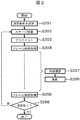
- FIG. 3 shows a processing flow diagram in a scanning electron microscope having a function of obtaining pattern information at the same time as the dimension calculation without reducing the throughput according to the present embodiment.
- the dimension calculation process is the same as that shown in FIG. 2.
- S301 to S304 are the same processes as S201 to S204.
- S301 in addition to the measurement conditions set in S201, a condition for acquiring pattern information is included.
- the frame image acquired in S305 and S306 is stored in the image storage unit 112 (S309 and 310). At this time, the frame image is stored in the moving image format in addition to the image format (S311).
- length measurement values are calculated for the frame images stored in S309 and S310 (S312 and 313). If the frame image has insufficient length measurement accuracy, the frame image is subjected to known image processing to improve the sharpness.
- image processing for improving the sharpness of an image a method of emphasizing an edge in an image using an image filter can be used. However, any method that improves measurement accuracy is not limited to an image filter. It may be applied.
- pattern information is acquired using the length measurement values of the frame images obtained in S312 and S313 (S314). Note that the processing from S309 to S314 can be executed using a stage movement time zone or the like. Therefore, even if these pattern information acquisition processes are added, the pattern dimension measurement throughput hardly decreases.
- pattern information is obtained by performing analysis for each frame.
- an image from which pattern information is obtained is an image obtained by integrating the number of frames less than the number of frames constituting the length measurement image, or an image of one frame or subframe. It may be used.
- An image for obtaining such pattern information is defined as a sorted image. The separated image formation is performed by the data processing unit.
- FIG. 4 shows an example of a GUI (Graphical User Interface) for setting an environment for acquiring pattern information in step S301 for setting pattern information acquisition conditions according to the present embodiment.
- GUI Graphic User Interface
- an image format and a moving image format can be selected.
- the capacity can be reduced from 1/5 to about 1/10 as compared with the image format.
- the moving image format generally uses the MPEG4 (Moving Picture Experts Group) format capable of high compression, but may be saved in another moving image format to match the format compatible with the image analysis software.
- the compression rate of the moving image can be selected. The compression rate can be specified by 8 bits from 0 to 255. The larger the compression rate, the more the moving image capacity can be reduced. However, since the image information is reduced, the data accuracy obtained is lowered.
- the data storage in the moving image format is intended to reduce the capacity while maintaining the data accuracy, and the optimum compression rate is determined by the data accuracy required for the acquired pattern information.
- the data accuracy must be increased by setting the compression rate low.
- the compression rate is set high in order to reduce the data capacity. Note that each item shown in FIG. 4 may be displayed in a plurality of screens instead of one screen.
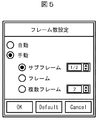
- FIG. 5 shows an example of a GUI for selecting the number of frames of the sorted image for analyzing pattern information.
- the number of frames can be selected from a subframe, a frame, and a plurality of frames, and the subframe and the plurality of frames can be set in more detail.
- the number of frames can be changed in accordance with the target pattern information, and the pattern information can be obtained with high accuracy by this change.
- the selection of the number of frames can be specified individually, but can be automatically set to an appropriate value according to the pattern information.
- the number of classified image frames appropriate for each pattern information will be described for each pattern information.
- step S314 for acquiring pattern information using a plurality of frame images according to the present embodiment will be described.
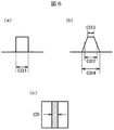
- FIG. 6 is a diagram showing length measurement values obtained for two pattern shapes. In the scanning electron microscope, these patterns are used to create an image using secondary electrons generated when an electron beam is irradiated from above, and dimension measurement is performed.
- FIG. 6C shows an example of an SEM image.
- the pattern dimension is measured as a length measurement value CD by detecting the edge portion of the pattern with various length measurement algorithms. Therefore, the length measurement value CD is highly sensitive to changes in the width of the pattern, but not sensitive to changes in the cross-sectional shape.
- CD1 is measured as a pattern dimension.
- the pattern dimension is generally measured by a distance CD2 between positions corresponding to half the height of the pattern.
- Dimension CD2 measured here is different from the top width CD3 and bottom width CD4 of the pattern. If CD1 and CD2 are the same, the two patterns in FIG. 6 are recognized as patterns having the same shape. The phenomenon that the pattern shapes are different even if the length measurement values obtained with such a scanning electron microscope are the same causes a problem when observing the resist pattern after development in the photolithography process.
- the post-development process is a lower layer etching process, and the bottom width of the resist pattern is important for the post-development pattern.
- the bottom width CD4 is the length measurement value CD2 obtained with the scanning electron microscope. Different. Therefore, in the pattern dimension management process using the scanning electron microscope, a technique for discriminating the difference in the cross-sectional shape of the resist pattern in addition to the calculation of the length measurement value is required.
- FIG. 7 shows the shrinkage of the resist that occurs when the two resist patterns shown in FIGS. 6A and 6B are irradiated with an electron beam, and the pattern dimensions measured at that time.
- the electron beam 120 is indicated by an arrow, and a region to be shrunk by irradiation of the electron beam 120 is indicated by oblique lines.
- FIG. 7A since the electron beam 120 is irradiated onto the pattern from above, the electron beam is irradiated almost on the upper surface and hardly irradiated on the side surface. Therefore, the amount of shrink on the upper surface of the pattern is large due to the amount of irradiation, but the amount of shrink on the side surface is small.
- the pattern dimension is CD5, which is slightly smaller than the length measurement value CD1 before shrinking.
- the shrink amount on the upper surface is the same as that in FIG. 7A because the irradiation amount of the electron beam 120 does not change, but the side surface receives the irradiation of the electron beam 120 over a wide area. Therefore, the amount of shrinkage becomes larger than that in FIG. 7A, and the length measurement value is greatly reduced from CD2 to CD6.
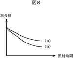
- FIG. 8 shows changes in the measured value as a function of the electron beam irradiation time for these two resist patterns.
- the same length measurement value is obtained although the cross-sectional shapes of the pattern (a) and the pattern (b) are different.
- the resist pattern shrinks. As described above, the size of the shrink differs between the patterns (a) and (b), and the length measurement value is a pattern (compared to the pattern (a) ( b) changes greatly.
- the specific usage method is to identify a pattern that has a different shape from the original, and set the amount of deviation from the reference data acquired in advance or the amount of deviation from the result obtained for the same type of pattern.
- the difference in shape is determined by comparing with the value. If there is a deviation from the set value, an error is displayed.
- the present invention can be applied not only to an electron beam but also to a microscope using an ion beam.
- the pattern information is acquired using the fractional images constituting the length measurement image, so that the pattern material and the three-dimensional structure can be obtained without reducing the pattern dimension measurement throughput.
- a charged particle beam microscope from which information can be obtained can be provided.
- the cross-sectional shape of the pattern can be estimated by obtaining the change over time of the length measurement value.
- the second embodiment will be described with reference to FIGS.
- the contents described in the first embodiment can also be applied to the present embodiment unless there are special circumstances.
- zero shrink estimation will be described.
- FIG. 9 shows the dimension measurement method before shrinking compared with the conventional method.
- FIG. 9 (a) shows a conventionally used method for calculating the zero time value
- FIG. 9 (b) shows the technique of the present invention.
- FIG. 9A a length measurement image obtained by scanning the observation location a plurality of times is obtained a plurality of times, and a length measurement value is calculated for each length measurement image. Plot the number of measurements on the horizontal axis and the measured value on the vertical axis. Since the resist pattern has a characteristic of shrinking when irradiated with an electron beam, the length measurement value gradually decreases with the number of measurements (elapse of irradiation time). Next, an approximate straight line is fitted to the measurement point, and the intercept with the vertical axis is calculated as a length measurement value before shrinking. This value is called the zero time value.
- This method can obtain high accuracy, but it takes time to measure because it is necessary to acquire a plurality of measurement images, and the accuracy of zero count is greatly affected by the fitting accuracy. Further, since the observed place is greatly shrunk, there is a problem that it becomes impossible to use as a circuit element after measuring the pattern dimension.
- FIG. 9B which is the present embodiment, will be described.
- length measurement is performed on the sorted images constituting the length measurement image, and the length measurement results are plotted in the same manner as in FIG.
- the condition closest to the zeroth value is the length measurement value of the first length measurement image, but here the length measurement value of the first sorted image is the zeroth time measurement value.
- the error from the value can be reduced.
- the length measurement value of the first sorted image is used, but the intercept with the vertical axis obtained by fitting an approximate curve to a plurality of length measurement values of the sorted image may be used. good.
- the length measurement accuracy of the separated image is lower than the length measurement accuracy of the length measurement image. Therefore, in order to improve the length measurement accuracy, the absolute value of the length measurement value is matched with the length measurement value of the length measurement image. May be. In order to further improve the accuracy, it is possible to use a method in which two length measurement images are acquired and the corresponding sorted images are plotted to match the absolute values. Therefore, it is possible to calculate the dimension of the zero count value with higher accuracy than before by calculating and measuring the length measurement value using the sorted image.
- Fig. 10 shows a processing flow diagram for analysis for each subframe.
- S1001 to S1008 have the same processing flow as S301 to S308.
- the frame images acquired in S1004 and S1005 are divided to create subframe images and stored in the image storage unit 112 (S1009 and S1010).
- the subframe image is saved in a moving image format (S1011).
- length measurement values are calculated for the subframe images stored in S1009 and S1010 (S1012 and S1013).
- image processing for improving the sharpness of an image a method of emphasizing an edge in an image using an image filter can be used.
- any method that improves measurement accuracy is not limited to an image filter. It may be applied.
- pattern information is acquired using the length measurement values of the sub-frame images obtained in S1012 and S1013 (S1014).
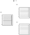
- FIG. 11 illustrates a method of creating a subframe image when using interlaced scanning, which is one of typical scanning methods.
- the number of scanning lines of the image is 16.
- Interlaced scanning is a method of forming an image by scanning odd lines of an image in order from the top and then scanning even lines in order from the top.
- an image obtained only by odd line scanning and an image obtained only by even line scanning are respectively subframe images.
- FIG. 11A is a frame image
- FIG. 11B is a subframe image obtained by scanning odd lines
- FIG. 11C is a subframe image obtained by scanning even lines.
- the method of dividing the image into the odd line scanning lines and the even line scanning lines which can grasp the whole image and can easily identify the pattern, has been described as a method for creating the subframe image. There are also ways to create images.
- the pattern information is acquired using the fractional images constituting the length measurement image, so that the pattern material and the three-dimensional structure can be obtained without reducing the pattern dimension measurement throughput.
- a charged particle beam microscope from which information can be obtained can be provided.
- the zero count value can be obtained from the relationship between the number of measurements of the sorted image and the length measurement value.
- the third embodiment will be described with reference to FIGS.
- the contents described in the first embodiment can also be applied to the present embodiment unless there are special circumstances.
- a method for determining whether a pattern is a remaining pattern (Line pattern) or a removed portion (Space pattern) with respect to a resist pattern will be described.
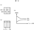
- Fig. 12 (a) shows an example image of the observed pattern.
- an example is shown in which there is no difference in the contrast between the Line portion and the Space portion.
- This method is not limited to this case, and the present method can be applied to the case where it is not possible to discriminate which pattern remains from the remaining part even if the light and shade are seen, or in the case of the pattern in which the light and dark contrast changes during observation.
- the length measurement values of CD1 and CD2 having adjacent pattern widths are measured.
- FIG. 12 (b) shows the result of observing the time change of the measured values of CD1 and CD2. As time elapses (increase in the number of frames), CD1 decreases and CD2 increases accordingly. Since the resist has a characteristic of shrinking with electron beam irradiation, it is possible to determine that the portion corresponding to CD1 is the resist and the portion corresponding to CD2 is the base.
- the obtained results are displayed as L (Line) and S (Space) at the top of the pattern as shown in FIG. However, even if it is not displayed in the pattern, it may be written which pattern is Line or Space in the image condition file, or the image may be displayed with a color.
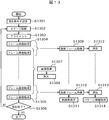
- Fig. 13 shows a processing flow diagram for analyzing multiple frames.
- S1301 to S1308 have the same processing flow as S301 to S308.
- a plurality of frame images are created by grouping the frame images acquired in S1304 and S1305 for each small group and stored in the image storage unit 112 (S1309, S1310).
- a plurality of frame images are stored in a moving image format (S1311).
- length measurement values are calculated for the multiple frame images stored in S1309 and S1310 (S1312, S1313).
- the multi-frame image can obtain higher length measurement accuracy than the frame image, but it is preferable to obtain higher length measurement accuracy by further improving the definition by performing image processing.
- image processing for improving the sharpness of an image a method of emphasizing an edge in an image using an image filter can be used.
- any method that improves measurement accuracy is not limited to an image filter. It may be applied.
- pattern information is acquired using the length measurement values of the plurality of frame images obtained in S1312, S1313 (S1314).
- the pattern information is acquired using the fractional images constituting the length measurement image, so that the pattern material and the three-dimensional structure can be obtained without reducing the pattern dimension measurement throughput.
- a charged particle beam microscope from which information can be obtained can be provided. In particular, it is possible to determine whether it is a remaining pattern (Line pattern) or a removed portion (Space pattern) with respect to the resist pattern from the change in length of the measurement value.
- the fourth embodiment will be described with reference to FIGS.
- the contents described in the first embodiment can also be applied to the present embodiment unless there are special circumstances.
- a method for estimating the material of a pattern will be described.
- FIG. 14A shows an example of an observed image.
- a method for examining which of a pattern in which a conductor and an insulator are mixed corresponds to a conductor will be described. Assume that the conductor and insulator materials are known. Such an object is often used in a photomask in which chromium as a conductor is patterned on a quartz substrate as an insulator.
- FIG. 14B shows the result of observing the temporal change of the gradation value for the pattern in which these conductors and insulators are mixed.
- the change in gradation value is greatly affected by the charged state of the sample surface. Since the charged state varies depending on the material of the sample, it is possible to determine the material of the sample by observing the change in gradation value.
- the charge on the sample surface is saturated in a short time after irradiation with the electron beam, whereas in the conductor, the charge gradually diffuses because the charge diffuses throughout the conductor.
- the gradation value changes abruptly in a short time in the insulator and then stagnates, while the gradation value changes gradually in the conductor. By examining such a change in gradation value, it is possible to determine which of the patterns is a conductor or an insulator.
- FIG. 15 shows a processing flow diagram in the present embodiment.
- S1501 to S1511 are the same processes as S301 to S311.
- S1512 and S1513 not the length measurement value but the gradation value of each pattern in the image is calculated. Pattern information is acquired using these gradation values (S1514).
- the pattern information is acquired using the fractional images constituting the length measurement image, so that the pattern material and the three-dimensional structure can be obtained without reducing the pattern dimension measurement throughput.
- a charged particle beam microscope from which information can be obtained can be provided.
- the fifth embodiment will be described with reference to FIGS.
- the contents described in the first embodiment can also be applied to the present embodiment unless there are special circumstances.
- FIG. 16 is a diagram showing a configuration of a scanning electron microscope in the present embodiment.
- moving image data obtained by a scanning electron microscope is transferred to an image processing server and developed into a still image in the image processing server to acquire pattern information.
- Image data stored in the image storage unit 112 of the control unit 102 of the scanning electron microscope is transferred to the image storage unit 1602 of the image processing server 1601 in a moving image format.
- the moving image data is expanded into a still image by the image expansion unit 1603, and pattern information is acquired by the data processing unit 1604.
- FIG. 17 shows a processing flowchart in the present embodiment.
- length measurement is performed at the same time as image acquisition and pattern information is acquired.
- pattern information acquisition is performed offline after transferring all image data to a server for a scanning electron microscope.
- S1701 to S1711 are the same processing flow as S301 to S311.
- the moving image data stored in S1711 is transferred to the image storage unit 1602 of the image processing server 1601 (S1712). Next, the transferred moving image data is expanded into a still image in order to analyze the image information (S1713), and pattern information is acquired (S1714).
- the image data is not analyzed by the control unit of the scanning electron microscope and the pattern information is acquired as in the first embodiment, but the image data is transferred to the image processing server for analysis. Transfer is an important issue. If the image data is a still image such as a frame image, the capacity is large and a load is imposed on data transfer. Therefore, the load of data transfer can be reduced by converting the still image into a moving image and compressing the capacity. Moreover, since the internal memory is not consumed for acquiring the pattern information, the load on the scanning electron microscope can be reduced.
- the pattern information is acquired using the fractional images constituting the length measurement image, so that the pattern material and the three-dimensional structure can be obtained without reducing the pattern dimension measurement throughput.
- a charged particle beam microscope from which information can be obtained can be provided.
- the load on the charged particle beam microscope can be reduced.
- a pattern material or a three-dimensional structure is formed by using an image accumulated from the obtained frame image and a fractional image consisting of one frame image or a sub-frame image.
- Charged particle beam microscope characterized by creating information on (2)
- a charged particle beam microscope according to (1), wherein the number of frames of the sorted image to be stored can be selected in accordance with information on the material of the pattern to be acquired and the three-dimensional structure.
- DESCRIPTION OF SYMBOLS 101 Electron microscope part, 102 ... Control part, 103 ... Display part, 104 ... Electron source, 105 ... Condensing lens, 106 ... Deflector, 107 ... Objective lens, 108 ... Sample, 109 ... Sample stand, 110 ... Detector, DESCRIPTION OF SYMBOLS 111 ... Data processing part, 112 ... Image storage part, 113 ... Arithmetic processing part, 114 ... Monitor, 120 ... Electron beam, 130 ... Secondary electron and reflected electron, 1601 ... Image processing server, 1602 ... Image storage part, 1603 ... Image development unit, 1604... Data processing unit.
Landscapes
- Physics & Mathematics (AREA)
- Electromagnetism (AREA)
- General Physics & Mathematics (AREA)
- Chemical & Material Sciences (AREA)
- Analytical Chemistry (AREA)
- Length-Measuring Devices Using Wave Or Particle Radiation (AREA)
Abstract
パターン寸法計測のスループットを低下させることなくパターンの材料や立体構造に関する情報を得ることができる荷電粒子線顕微鏡を提供するために、荷電粒子線顕微鏡において、試料の観察視野を走査して得られたフレーム画像を複数枚取得し(S304、S305)、それらの画像を積算し(S307)、試料上に形成されたパターンの寸法を算出(S308)すると共に、フレーム画像を構成する1フレーム画像またはサブフレーム画像等からなる分別画像(S309,S310)を用いてパターン情報を取得する(S314)。
Description
本発明は、荷電粒子線顕微鏡装置に係り、特に、電子線を照射することによって形状の変化や帯電が生じる試料を測定の対象とする走査電子顕微鏡を含む荷電粒子線顕微鏡に関する。
荷電粒子線顕微鏡、例えば走査電子顕微鏡は、試料に細く絞った電子線を照射し、電子線照射により発生した二次電子や反射電子を検出し、検出信号を元に輝度変調して画像を形成する装置である。
半導体製造工程においては、パターンの微細化に伴い、高い計測精度を持つ装置が必要とされている。光学式の計測装置では計測できない数十ナノメートルオーダーの微細パターンの幅を計測する寸法計測ツールとしては、それらのパターンを10万倍以上の拡大倍率で撮像可能なパターン幅計測用の走査電子顕微鏡(測長SEM(Scanning Electron Microscope))が用いられている。
このような目的で用いられる走査電子顕微鏡においては、一般に観察対象となるパターンを含む領域を走査して得られたフレーム画像を複数枚積算して測長画像を作成し、得られた測長画像を様々な測長アルゴリズムを用いて解析することでパターンの寸法を高い精度で算出している。ここでは、観察視野を一度走査して得られた画像をフレーム画像、複数枚のフレーム画像を積算した画像を測長画像と定義している。
測長SEMは半導体基板上に作成されたパターンの寸法を計測する目的で用いられているが、前記用途に加えて測長画像を複数枚取得して取得画像の経時変化を観察することで材料や立体構造などのパターン情報が得られている。電子線の照射により経時変化するパターン情報の代表例として、レジストパターンのシュリンクや試料表面の帯電があげられる。これらの経時変化情報を用いたパターン情報の取得は、レジストのシュリンク量の計測やLine-Space判定、材料推定に活用されている。
近年の半導体デバイスの作成で使用されているArF(波長193nm)露光機対応のフォトレジストは、電子線の照射によりダメージを受けて体積の収縮(シュリンク)が生じることが課題となっている。半導体素子が設計どおりの性能を実現するためには、半導体製造工程において回路パターンの形状や寸法を厳しく管理することが必要であるが、走査電子顕微鏡を用いてレジストパターンを観察すると、シュリンクが発生してパターンが有する本来の寸法を正しく計測できなかった。
この課題を解決するために、特許文献1ではパターンに垂直なX方向より水平なY方向を低倍率に設定して電子線の照射密度を低下させることでシュリンクの発生を抑制し、正確なパターンの寸法測定を算出している。また、特許文献2では、シュリンクが発生しても測長値とシュリンクの経過を示す近似関数を実験値にフィッティングさせることでシュリンク前の寸法を算出している。
また、レジストは基材がアクリル樹脂等の絶縁体で構成されているため、電子線を照射すると試料表面に電荷が蓄積した帯電状態となる。帯電が発生すると濃淡コントラストが変化してしまい、測定しようとしているパターンが残しパターン(Lineパターン)なのか抜き部分(Spaceパターン)なのか判別できなくなる。この課題を解決するために、特許文献3では2枚のレジストパターン画像に対して、レジストパターンの内側寸法と外側寸法を計測し、測長値の比較によってレジストパターンが残し部と抜き部のどちらかであるかを判定している。
また、特許文献4では基板上の帯電が平衡状態に達するまでの電子ビームの走査回数に対応する反射電子の信号波形を測定し、既知物質のデータと比較することで未知物質を同定することを可能としている。
上記従来技術により走査電子顕微鏡を用いて寸法情報に加えてパターン情報の取得が可能となっているものの、これらの技術ではパターン情報の取得に測長画像を複数枚取得することが必要であり、スループットの低下を生じさせていた。
本発明の目的は、パターン寸法計測のスループットを低下させることなく、パターンの材料や立体構造に関する情報を得ることのできる荷電粒子線顕微鏡を提供することにある。
上記目的を達成するための一実施形態として、荷電粒子源と、試料台と、前記荷電粒子源から放出された荷電粒子の照射に因る前記試料台上に配置される試料からの荷電粒子を検出する検出部と、を有する顕微鏡部と、前記検出器からの検出信号のフレーム画像への変換や複数の前記フレーム画像を積算して測長画像とするデータ処理部と、前記フレーム画像を保存する画像記憶部と、前記測長画像から前記試料上に形成されたパターンの寸法を求める演算処理部とを有する制御部と、を備えた荷電粒子線顕微鏡であって、前記データ処理部は、前記測長画像を構成するフレーム枚数より少ないフレーム数で積算した複数フレーム画像や1フレーム画像またはサブフレーム画像を分別画像として形成する機能を有することを特徴とする荷電粒子線顕微鏡とする。
また、試料の観察視野を走査して得られたフレーム画像を複数枚取得し、複数枚のフレーム画像を積算して作成した測長画像を用いて試料上に形成されたパターンの寸法を算出する荷電粒子線顕微鏡において、得られたフレーム画像から形成される、取得したフレーム枚数より少ないフレーム数で積算した画像や1フレーム画像またはサブフレーム画像からなる分別画像を用いてパターンの材料や立体構造に関する情報を作成することを特徴とする荷電粒子線顕微鏡とする。
測長画像を構成する画像(分別画像)を用いることで、パターン寸法計測のスループットを低下させることなく、パターンの材料や立体構造に関するパターン情報が得られる荷電粒子線顕微鏡を提供することができる。
以下、実施例により説明する。
第1の実施例について、図1から図8を用いて説明する。図1は本実施例に係る走査電子顕微鏡の構成を示す図である。この装置は、フレーム画像の積算による測長画像の作成と測長機能、測長画像を構成する複数枚のフレーム画像の経時変化からパターン情報を取得することを可能とするものである。ここで、観察視野を一度走査して得られたフレーム画像を複数枚積算して作成した画像を測長画像と定義する。
パターン情報を取得する機能を備えた走査電子顕微鏡は、電子顕微鏡部101、制御部102、表示部103から構成されている。電子源104から放出された電子線120は、集束レンズ105、対物レンズ107で収束された後に試料台109に載置された試料108に照射される。電子線は偏向器106により、試料上を二次元的に走査される。試料から発生した二次電子や反射電子130は、検出器110で検出され、データ処理部111で信号を輝度変調してフレーム画像に変換し、画像記憶部112に格納される。
画像記憶部112に保存されたフレーム画像は、複数枚の経時変化から演算処理部113においてパターン情報が取得される。また、パターン情報の取得と同時にデータ処理部111において画像記憶部112に保存された複数枚のフレーム画像が積算され、測長画像が得られる。
その後、測長画像にパターン情報が追加され、モニタ114に表示する。この際、演算処理部113にて測長画像からパターン寸法を算出する。パターン情報は画像に追加しても良いが、測長画像の条件ファイルにテキストデータとして追加しても良い。データ処理部111及び演算処理部113の機能はCPUにてそれぞれ実行可能であり、前記画像記憶部112はCPUに接続されるメモリ部に設けることができる。なお、それぞれを専用ハードで構成してもよい。
走査電子顕微鏡を用いた計測では、一般に観察視野を複数回走査して得られた測長画像が用いられる。ここでの「計測」とは、例えば半導体ウエハ上に形成されたパターン寸法の算出である。試料を複数回走査して得られた測長画像は、1回だけ走査して得られたフレーム画像に較べてS/N比の良い画像となるため高い測長精度が得られるが、複数回走査している間に試料の形状や帯電分布が変化したとしても、これらのパターンに関する情報は失われて平均化された情報だけが得られている。測長用の走査電子顕微鏡は観察パターンの寸法算出が目的であるため、このような使用方法が用いられているが、今後、寸法計測と同時にパターン情報の入手が必要となるため、本実施例では一般的な走査電子顕微鏡に新たにパターン情報を得る機能を追加している。
図2は従来の走査電子顕微鏡を用いてパターン寸法を計測する手順を示すフロー図である。以下にこのフロー図について説明する。
まず、測定条件を設定する(S201)。ここで、測定条件とは加速電圧などの装置条件や測定点の座標、パターンの形状、測長条件などである。次に、ステージを動かして測定点に移動する(S202)。次に、偏向器106により電子線の照射位置を微調整して目的のパターンが視野に含まれるように調整する(S203)。もし、ステージ移動精度が十分であればステップS203は行わなくても良い。
次に、同一視野においてフレーム画像をS201で設定した枚数分を連続して取得する(S204、S205)。あらかじめ設定された画像枚数が取得されたら測定を終了するか判定し(S206)、もし他に取得すべきデータがあればS202に戻り、同じ工程を繰り返す。
また、前記ステップと同時にS204、S205で取得されたフレーム画像を積算して測長画像を作成し(S207)、画像記憶部112に保存する。この際、フレーム画像は上書きされるため画像記憶部112には保存されない。最後に、S207で得られた測長画像を用いてパターンの寸法を算出する(S208)。
次に、本実施例であるスループットを低下させることなく寸法算出と同時にパターン情報を得ることができる機能を有する走査電子顕微鏡での処理フロー図を図3に示す。寸法算出の工程については図2と同じであり、ここでは新たな機能として加わったパターン情報の取得機能に対応する処理フローについて説明する。S301乃至S304はS201乃至S204と同じ処理である。S301ではS201で設定した測定条件に加え、パターン情報を取得する条件を含む。
まず、S305、S306で取得したフレーム画像を画像記憶部112に保存する(S309、310)。この際、フレーム画像は画像形式に加えて、動画像形式でも保存を行う(S311)。
次に、S309、S310で保存したフレーム画像に対して測長値を算出する(S312、313)。フレーム画像では測長精度が十分でない場合は、フレーム画像に公知の画像処理を行って鮮明度を向上させる。画像の鮮明度を向上させる画像処理としては、画像フィルタを用いて画像内のエッジを強調する手法などを取ることができるが、画像フィルタに限らず測定精度が向上する手法であればどの手法を適用しても良い。
最後に、S312、S313で得られたフレーム画像の測長値を用いてパターン情報を取得する(S314)。なお、S309からS314の処理は、ステージ移動の時間帯等を利用して実行することができる。そのため、これらパターン情報取得の処理が追加されてもパターン寸法計測のスループットの低下はほとんど生じない。
本実施例ではフレームごとに解析を行ってパターン情報を得ているが、パターン情報を得る画像は測長画像を構成するフレーム枚数より少ないフレーム数で積算した画像や1フレームまたはサブフレームの画像を用いても良い。このようなパターン情報を得るための画像を分別画像と定義する。なお、分別画像形成はデータ処理部で行なわれる。
本実施例のパターン情報の取得条件を設定するステップS301について、パターン情報の取得を行う環境設定を行うGUI(Graphical User Interface)の一例を図4に示す。まず、画像観察時に取得するパターン情報を選択する。パターン情報は、形状推定、ゼロシュリンク測定、Line-Space判定、材料推定が選択可能となっており、複数のパターン情報を同時に得ることも可能となっている。
また、パターン情報を取得する際に用いた分別画像を保存するか否か選択が可能となっている。保存形式は画像形式と動画像形式が選択でき、動画像形式では画像形式に較べて容量を1/5から1/10程度まで低減することができる。動画像形式は一般的に高圧縮が可能なMPEG4(Moving Picture Experts Group)形式を用いるが、画像解析ソフトとの対応形式に合わせるために他の動画像形式で保存しても良い。また、動画像の圧縮率も選択が可能である。圧縮率は0乃至255の8ビットで指定することができ、圧縮率を大きくするほど動画像の容量を低減することができるが、画像情報が減るために得られるデータ精度は低下する。
動画像形式でのデータ保存はデータ精度を維持しつつ容量を低減することが目的であり、最適な圧縮率は取得するパターン情報に必要なデータ精度によって決まる。例えば、レジストパターンの立体形状の差を調べる手法では二つのパターンにおける測長値の変化量の差を計測することが必要であることから、圧縮率を低く設定してデータ精度を高めなければならない。一方、Line-Space判定では測長値が増加あるいは減少する特性が判別できれば良いのでデータ容量を低減するために圧縮率は高く設定する。なお、図4に示した各項目は、一画面ではなく複数画面に分けて表示してもよい。
パターン情報を解析するための分別画像のフレーム数を選択するためのGUIの一例を図5に示す。フレーム数は、サブフレーム、フレーム、複数フレームが選択可能となっており、サブフレームと複数フレームはさらに詳細な設定が可能となっている。フレーム数は目的とするパターン情報に合わせて変更することができ、この変更により高い精度でパターン情報を得ることができる。フレーム数の選択は個々に指定することも可能であるが、パターン情報に応じて自動的に適切な値に設定することも可能である。それぞれのパターン情報に適切な分別画像のフレーム数についてはパターン情報ごとに説明する。
本実施例の複数枚のフレーム画像を用いてパターン情報を取得するステップS314について、得られるパターン情報についてそれぞれ説明する。
図6は二つのパターン形状について得られる測長値を表した図である。走査電子顕微鏡ではこれらのパターンに対して上方から電子線を照射したときに発生する二次電子を用いて画像を作成して寸法計測を行う。図6(c)にSEM画像の例を示す。
パターン寸法はパターンのエッジ部分を様々な測長アルゴリズムで検出することで測長値CDとして計測される。したがって、測長値CDはパターンの幅の変化に対する感度は高いが、断面形状の変化に対しては感度が高くない。例えば、図6(a)のようなテーパーのないパターンにおいては、CD1がパターン寸法として計測される。一方、図6(b)のように順テーパーのパターンにおいては、パターン寸法は一般的にパターンの高さの半分に相当する位置間の距離CD2で計測される。
ここで計測された寸法CD2はパターンのトップ幅CD3やボトム幅CD4とは異なる。もし、CD1とCD2が同じ場合、図6の二つのパターンは同じ形状を持つパターンとして認識されてしまう。このような走査電子顕微鏡で得られた測長値が同じであってもパターン形状が異なる現象は、フォトリソグラフィ工程における現像後のレジストパターンの観察時に問題となる。
現像後の工程は下層のエッチング工程であり、現像後のパターンではレジストパターンのボトム幅が重要となる。図6(a)では得られた測長値がそのままパターンのボトム幅に相当するため問題はないが、図6(b)ではボトム幅CD4は走査電子顕微鏡で得られた測長値CD2とは異なる。したがって、走査電子顕微鏡を用いたパターン寸法の管理工程において、測長値の算出に加えてレジストパターンの断面形状の差を判別する技術が必要となる。
図6(a)(b)で示した二つのレジストパターンについて、電子線を照射したときに生じるレジストのシュリンク、及びその際に計測されるパターン寸法を図7に示す。電子線120は矢印で示しており、電子線120の照射によってシュリンクする領域は斜線で表している。まず、図7(a)では、電子線120はパターンに対して上方から照射されるため、電子線はほぼ上面に照射され側面にはほとんど照射されない。したがって、照射量の大きさからパターンの上面のシュリンク量は大きいが側面のシュリンク量は小さい。このとき、パターン寸法はCD5となり、シュリンク前の測長値CD1に較べてわずかに小さくなる特性を持つ。
一方、図7(b)のパターンにおいては上面のシュリンク量は図7(a)と電子線120の照射量が変わらないために同じであるが、側面は電子線120の照射を広い領域にわたって受けるために図7(a)に較べてシュリンク量が大きくなり、測長値はCD2からCD6と大きく減少する。
これら二つのレジストパターンに対して電子線の照射時間を関数とした測長値変化を図8に示す。ここでは、パターン(a)とパターン(b)の断面形状が異なるが同じ測長値が得られた場合を仮定している。これらのパターンに対して電子線を照射するとレジストパターンはシュリンクし、前述したようにシュリンクの大きさはパターン(a)と(b)で異なり、測長値はパターン(a)に較べてパターン(b)が大きく変化する。
このようにシュリンク量の違いを観察することで、フォトリソグラフィ工程における現像後のレジストパターンに対して、測長値だけでなく断面形状の違いを検出することでパターン管理の精度を向上させることが可能となる。具体的な使用方法としては、本来とは異なる形状となっているパターンを識別することであり、あらかじめ取得していたリファレンスデータからのずれ量、あるいは同種パターンについて取得した結果からのずれ量を設定値と比較することで形状の差を判定する。もし設定値よりずれていた場合にはエラー表示をする。
このような目的では、シュリンクによる測長値変化曲線の差が二種類のパターンで判別できることが重要である。したがって、フレーム数は測長値の変化が認識できるように細かく分割すること、および測長精度が十分保たれていることが必要であることから、1フレームごとに解析をすることが好ましい。
また、画像を動画形式で保存することで異なる時間でのパターン情報の取得が可能となる。これにより、プロセスに異常が発見された場合の解析が容易となる、時間を掛けて複数のパターン情報を取得できる、などのメリットを得ることが出来る。逆に、このような解析を行わない場合には分別画像や動画像の保存の必要はなく、最終的に測長に用いる加算画像と取得されたパターン情報のみ保存することで、システムを簡素化できる。
以上電子線を用いた場合について説明したが、電子線に限らずイオンビームを用いた顕微鏡にも適用することができる。
以上述べたように、本実施例によれば、測長画像を構成する分別画像を用いてパターン情報を取得することで、パターン寸法計測のスループットを低下させることなく、パターンの材料や立体構造に関する情報が得られる荷電粒子線顕微鏡を提供することができる。特に、測長値の経時変化を求めることによりパターンの断面形状を推定できる。
第2の実施例について図9、図10を用いて説明する。なお、実施例1に記載の内容は特段の事情がない限り、本実施例にも適用できる。本実施例ではゼロシュリンク推定について説明する。
図9に従来手法と比較したシュリンク前の寸法計測方法を示す。図9(a)は従来から用いられてきたゼロ回値の算出方法を、図9(b)に本発明の手法を示している。
まず、図9(a)について説明する。まず、観察箇所を複数回走査して得られた測長画像を取得することを複数回行い、それぞれの測長画像で測長値を算出する。横軸に測定回数、縦軸に測長値をプロットする。レジストパターンでは電子線の照射によりシュリンクする特性が見られることから、測定回数(照射時間の経過)とともに測長値は徐々に減少する。次に、測定点に対して近似直線をフィッティングして縦軸との切片をシュリンク前の測長値として算出する。この値をゼロ回値と呼ぶ。
この手法は高い精度が得られるが、測長画像を複数枚取得する必要があるために計測に時間がかかり、またゼロ回値の精度がフィッティング精度に大きく影響を受ける。さらに、観察した場所は大きくシュリンクするためにパターン寸法の計測後に回路素子として使えなくなるといった課題が生じている。
次に、本実施例である図9(b)について説明する。ここでは、測長画像を構成する分別画像で測長を行っており、測長結果を図9(a)と同様にプロットしている。図9(a)ではゼロ回目の値に最も近い条件は1枚目の測長画像の測長値であるが、ここでは1枚目の分別画像の測長値となっており、ゼロ回目の値からのエラーを小さくすることができている。ゼロ回値の大きさは、1枚目の分別画像の測長値を用いるが、分別画像の複数個の測長値に近似曲線をフィッティングして得られた縦軸との切片を用いても良い。
ここで、分別画像の測長精度は測長画像の測長精度に較べて低下しているので、測長精度を高めるために、測長値の絶対値を測長画像の測長値に合わせても良い。さらに精度を高めるためには、測長画像を二枚取得し、それに対応する分別画像をプロットして絶対値を合わせる手法を用いることができる。したがって分別画像を用いて測長値算出して調べることでゼロ回値の寸法をこれまでより高い精度で算出することが可能となる。
このような目的では、測長値を細かく調べることが重要であり、フレーム数をなるべく小さくすることが必要であり、1フレームあるいはサブフレームごとに解析をすることが好ましい。
サブフレームごとに解析する処理フロー図を図10に示す。S1001乃至S1008はS301乃至S308と同じ処理フローとなっている。
まず、S1004、S1005で取得したフレーム画像を分割してサブフレーム画像を作成して画像記憶部112に保存する(S1009、S1010)。次に、サブフレーム画像を動画像形式で保存を行う(S1011)。
次に、S1009、S1010で保存したサブフレーム画像に対して測長値を算出する(S1012、S1013)。サブフレーム画像では測長精度が十分でない場合は、サブフレーム画像に画像処理を行って鮮明度を向上させることが好ましい。画像の鮮明度を向上させる画像処理としては、画像フィルタを用いて画像内のエッジを強調する手法などを取ることができるが、画像フィルタに限らず測定精度が向上する手法であればどの手法を適用しても良い。
最後に、S1012、S1013で得られたサブフレーム画像の測長値を用いてパターン情報を取得する(S1014)。
図11には代表的な走査方法の一つであるインターレス走査を用いた場合のサブフレーム画像の作成方法について説明する。簡単のため、画像の走査ライン数は16にしている。インターレス走査とは、画像の奇数ラインを上から順番に走査した後に偶数ラインを上から順番に走査して1枚の画像を形成する手法である。ここでは、奇数ライン走査のみで得られる画像と偶数ライン走査のみで得られる画像をそれぞれサブフレーム画像とした。
図11(a)はフレーム画像であり、図11(b)は奇数ラインの走査で得られるサブフレーム画像、図11(c)は偶数ラインの走査で得られるサブフレーム画像である。本実施例ではサブフレーム画像の作成方法として画像の全体像を把握可能でパターンの同定が容易な奇数ライン走査線と偶数ライン走査線に分ける方法を説明したが、画像を上下に分けてサブフレーム画像を作成する方法などもある。
以上述べたように、本実施例によれば、測長画像を構成する分別画像を用いてパターン情報を取得することで、パターン寸法計測のスループットを低下させることなく、パターンの材料や立体構造に関する情報が得られる荷電粒子線顕微鏡を提供することができる。特に、分別画像の測定回数と測長値との関係からゼロ回値を求めることができる。
第3の実施例について図12、図13を用いて説明する。なお、実施例1に記載の内容は特段の事情がない限り、本実施例にも適用できる。本実施例ではレジストパターンに対してパターンが残しパターン(Lineパターン)なのか抜き部分(Spaceパターン)なのか判別するための手法について説明する。
図12(a)に観察されるパターンの画像例を示す。ここではLine部分とSpace部分の濃淡コントラストに差が見られない例を示している。この場合に限らず、濃淡が見られてもどちらが残しパターンと抜き部分か判別できない場合や、観察途中に濃淡コントラストが変化するようなパターンの場合に本手法は適用が可能である。この課題を解決するために、本実施例では隣り合うパターン幅のCD1とCD2の測長値を計測する。
これらCD1とCD2の測長値の時間変化を観察した結果を図12(b)に示す。時間経過(フレーム数の増加)とともにCD1は減少し、それに従ってCD2は増加する。レジストは電子線の照射とともにシュリンクする特性を持っていることから、CD1に相当する部分がレジスト、一方、CD2に相当する部分が下地と判別することができる。
得られた結果を図12(c)に示すようにパターンの上部にL(Line)、S(Space)と表示する。しかし、パターンに表示しなくても、画像の条件ファイルにどちらのパターンがLineかSpaceか書き込んでも良いし、画像に色を塗って表示しても良い。
このような目的では、二つの測長値CD1、CD2が増加するか減少するか判別できれば十分であり、フレーム数を加算して測長精度を高めることが必要なので、4フレーム以上の複数フレーム画像を用いて解析をすることが好ましい。
複数フレームごとに解析する処理フロー図を図13に示す。S1301乃至S1308はS301乃至S308と同じ処理フローとなっている。
まず、S1304、S1305で取得したフレーム画像を小グループごとにまとめて複数フレーム画像を作成して画像記憶部112に保存する(S1309、S1310)。次に、複数フレーム画像を動画像形式で保存を行う(S1311)。次に、S1309、S1310で保存した複数フレーム画像に対して測長値を算出する(S1312、S1313)。
複数フレーム画像はフレーム画像と較べて高い測長精度が得られるが、画像処理を行ってさらに鮮明度を向上させることでより高い測長精度を得ることが好ましい。画像の鮮明度を向上させる画像処理としては、画像フィルタを用いて画像内のエッジを強調する手法などを取ることができるが、画像フィルタに限らず測定精度が向上する手法であればどの手法を適用しても良い。
最後に、S1312、S1313で得られた複数フレーム画像の測長値を用いてパターン情報を取得する(S1314)。
以上述べたように、本実施例によれば、測長画像を構成する分別画像を用いてパターン情報を取得することで、パターン寸法計測のスループットを低下させることなく、パターンの材料や立体構造に関する情報が得られる荷電粒子線顕微鏡を提供することができる。特に、測長値の時間変化からレジストパターンに対する残しパターン(Lineパターン)なのか抜き部分(Spaceパターン)なのか判別することができる。
第4の実施例について図14、図15を用いて説明する。なお、実施例1に記載の内容は特段の事情がない限り、本実施例にも適用できる。本実施例ではパターンの材料推定する手法について説明する。
図14(a)は観察された画像の一例を示している。ここでは代表的な例として、導体と絶縁体が混ざっているようなパターンについてどちらが導体に対応するか調べる方法について説明する。導体と絶縁体の材料は既知であると仮定する。このような目的は、絶縁体である石英基板の上に導体であるクロムがパターニングされているフォトマスクにおいてよく用いられる。
これら導体と絶縁体が混ざったパターンに対して階調値の時間変化を観察した結果を図14(b)に示す。階調値の変化は試料表面の帯電状態に大きく影響を受ける。試料の材質によって帯電状態は変わるので、階調値の変化を観察すれば試料の材質を判別することが可能となる。絶縁体では試料表面の帯電は電子線を照射して短い時間で飽和するのに対して、導体では電荷が導体全体に拡散するので帯電は緩やかに進行する。すなわち、階調値は絶縁体では短い時間で急激に変化してその後は停滞するのに対して、導体では緩やかに変化していく特徴が見られる。このような階調値の変化を調べることでパターンのどちらが導体か絶縁体か判別することが可能となる。
得られた結果は図14(c)に示すようにパターンの上部にC(Conductor)、I(Insulator)と表示する。しかし、パターンに表示しなくても、画像の条件ファイルにどちらのパターンが導体か絶縁体か書き込んでも良いし、画像に色を塗って表示しても良い。ここではフォトマスクを仮定して導体か絶縁体か表示していたが、材質ごとに帯電の特性が異なるので、材質ごとの特性を記述したリファレンスをもとに材質を推定して画像の条件ファイルに書き込んでも良い。
このような目的では、階調値の変化量の差が二つのパターンで判別できることが重要であり、ある程度フレーム数を細かく分割することが必要であり、1フレームあるいはサブフレームごとに解析をすることが好ましい。
図15に本実施例における処理フロー図を示す。S1501乃至S1511はS301乃至S311と同じ処理である。S1512とS1513では測長値ではなく画像内の各パターンの階調値を算出している。これらの階調値を用いてパターン情報を取得する(S1514)。
以上述べたように、本実施例によれば、測長画像を構成する分別画像を用いてパターン情報を取得することで、パターン寸法計測のスループットを低下させることなく、パターンの材料や立体構造に関する情報が得られる荷電粒子線顕微鏡を提供することができる。特に、階調値の時間変化からパターンが導体か絶縁体か判別することができる。
第5の実施例について図16、図17を用いて説明する。なお、実施例1に記載の内容は特段の事情がない限り、本実施例にも適用できる。
図16は本実施例における走査電子顕微鏡の構成を示す図である。本実施例では走査電子顕微鏡で得られた動画像データを画像処理サーバに転送し、画像処理サーバ内で静止画像に展開してパターン情報の取得を行う。走査電子顕微鏡の制御部102の画像記憶部112に保存された画像データは動画像形式で画像処理サーバ1601の画像記憶部1602に転送される。動画像データは画像展開部1603において静止画像に展開され、データ処理部1604においてパターン情報が取得される。
図17に本実施例における処理フロー図を示す。図3では画像取得時と同時に測長を行い、パターン情報の取得を行っていたが、本実施例ではパターン情報の取得は全画像データを走査電子顕微鏡用のサーバに転送してからオフラインで行う。S1701乃至S1711はS301乃至S311と同じ処理フローである。
S1711で保存された動画像データは画像処理サーバ1601の画像記憶部1602に転送される(S1712)。次に、転送された動画像データは画像情報を解析するために静止画像に展開され(S1713)、パターン情報が取得される(S1714)。
本実施例では実施例1のように画像データを走査電子顕微鏡の制御部で解析してパターン情報を取得するのではなく、画像データを画像処理サーバに転送して解析を行うため、画像データの転送が重要な課題となる。画像データがフレーム画像などの静止画像では容量が大きくデータ転送における負荷がかかるため、静止画像を動画像に変換して容量を圧縮することでデータ転送の負荷を低減することができる。また、パターン情報の取得に内部メモリを消費することはないので、走査電子顕微鏡への負荷も低減することができる。
以上述べたように、本実施例によれば、測長画像を構成する分別画像を用いてパターン情報を取得することで、パターン寸法計測のスループットを低下させることなく、パターンの材料や立体構造に関する情報が得られる荷電粒子線顕微鏡を提供することができる。また、パターン情報の取得に内部メモリを消費することはないので、荷電粒子線顕微鏡への負荷も低減することができる。
以上、本願発明を詳細に説明したが、以下に主な発明の形態を列挙する。
(1)試料の観察視野を走査して得られたフレーム画像を複数枚取得し、複数枚のフレーム画像を積算して作成した測長画像を用いて試料上に形成されたパターンの寸法を算出する荷電粒子線顕微鏡において、得られたフレーム画像から形成される、取得したフレーム枚数より少ないフレーム数で積算した画像や1フレーム画像またはサブフレーム画像からなる分別画像を用いてパターンの材料や立体構造に関する情報を作成することを特徴とする荷電粒子線顕微鏡。
(2)前項(1)記載の荷電粒子線顕微鏡において、取得するパターンの材料や立体構造に関する情報に応じて保存する分別画像のフレーム数を選択できることを特徴とする荷電粒子線顕微鏡。
(3)前項(1)記載の荷電粒子線顕微鏡において、前記分別画像を動画圧縮技術を用いて動画像形式で保存することを特徴とする荷電粒子線顕微鏡。
(4)前項(3)記載の荷電粒子線顕微鏡において、取得するパターンの材料や立体構造に関する情報に応じて動画像の圧縮率を選択できることを特徴とする荷電粒子線顕微鏡。
(5)前項(1)記載の荷電粒子線顕微鏡において、荷電粒子線の照射によるレジストのシュリンクの大きさの違いから、レジストパターンの立体構造の差を推定することを特徴とする荷電粒子線顕微鏡。
(6)前項(1)記載の荷電粒子線顕微鏡において、複数フレーム内でのパターン寸法の変化から初期のパターン寸法を算出することを特徴とする荷電粒子線顕微鏡。
(7)前項(1)記載の荷電粒子線顕微鏡において、複数フレーム内での二箇所以上のパターン寸法の変化からレジストパターンの抜き部か残し部かを判定することを特徴とする荷電粒子線顕微鏡。
(8)前項(1)記載の荷電粒子線顕微鏡において、複数フレーム内での階調値の変化から材料を推定することを特徴とする荷電粒子線顕微鏡。
(1)試料の観察視野を走査して得られたフレーム画像を複数枚取得し、複数枚のフレーム画像を積算して作成した測長画像を用いて試料上に形成されたパターンの寸法を算出する荷電粒子線顕微鏡において、得られたフレーム画像から形成される、取得したフレーム枚数より少ないフレーム数で積算した画像や1フレーム画像またはサブフレーム画像からなる分別画像を用いてパターンの材料や立体構造に関する情報を作成することを特徴とする荷電粒子線顕微鏡。
(2)前項(1)記載の荷電粒子線顕微鏡において、取得するパターンの材料や立体構造に関する情報に応じて保存する分別画像のフレーム数を選択できることを特徴とする荷電粒子線顕微鏡。
(3)前項(1)記載の荷電粒子線顕微鏡において、前記分別画像を動画圧縮技術を用いて動画像形式で保存することを特徴とする荷電粒子線顕微鏡。
(4)前項(3)記載の荷電粒子線顕微鏡において、取得するパターンの材料や立体構造に関する情報に応じて動画像の圧縮率を選択できることを特徴とする荷電粒子線顕微鏡。
(5)前項(1)記載の荷電粒子線顕微鏡において、荷電粒子線の照射によるレジストのシュリンクの大きさの違いから、レジストパターンの立体構造の差を推定することを特徴とする荷電粒子線顕微鏡。
(6)前項(1)記載の荷電粒子線顕微鏡において、複数フレーム内でのパターン寸法の変化から初期のパターン寸法を算出することを特徴とする荷電粒子線顕微鏡。
(7)前項(1)記載の荷電粒子線顕微鏡において、複数フレーム内での二箇所以上のパターン寸法の変化からレジストパターンの抜き部か残し部かを判定することを特徴とする荷電粒子線顕微鏡。
(8)前項(1)記載の荷電粒子線顕微鏡において、複数フレーム内での階調値の変化から材料を推定することを特徴とする荷電粒子線顕微鏡。
101…電子顕微鏡部、102…制御部、103…表示部、104…電子源、105…集束レンズ、106…偏向器、107…対物レンズ、108…試料、109…試料台、110…検出器、111…データ処理部、112…画像記憶部、113…演算処理部、114…モニタ、120…電子線、130…二次電子や反射電子、1601…画像処理サーバ、1602…画像記憶部、1603…画像展開部、1604…データ処理部。
Claims (19)
- 荷電粒子源と、試料台と、前記荷電粒子源から放出された荷電粒子の照射に因る前記試料台上に配置される試料からの荷電粒子を検出する検出部と、を有する顕微鏡部と、
前記検出器からの検出信号のフレーム画像への変換や複数の前記フレーム画像を積算して測長画像とするデータ処理部と、前記フレーム画像を保存する画像記憶部と、前記測長画像から前記試料上に形成されたパターンの寸法を求める演算処理部とを有する制御部と、を備えた荷電粒子線顕微鏡であって、
前記データ処理部は、前記測長画像を構成するフレーム枚数より少ないフレーム数で積算した複数フレーム画像や1フレーム画像またはサブフレーム画像を分別画像として形成する機能を有することを特徴とする荷電粒子線顕微鏡。 - 請求項1に記載の荷電粒子線顕微鏡において、
前記分別画像のフレーム数は、取得する前記パターンの材料や立体構造に関する情報に応じて選択されるものであることを特徴とする荷電粒子線顕微鏡。 - 請求項1に記載の荷電粒子線顕微鏡において、
前記分別画像は、動画圧縮技術を用いて動画像形式で前記画像記憶部に保存されるものであることを特徴とする荷電粒子線顕微鏡。 - 請求項3に記載の荷電粒子線顕微鏡において、
前記動画像の圧縮率は、取得する前記パターンの材料や立体構造に関する情報に応じて選択されるものであることを特徴とする荷電粒子線顕微鏡。 - 請求項1に記載の荷電粒子線顕微鏡において、
前記試料上に形成されたパターンはレジストパターンであり、前記レジストパターンの立体構造は、前記分別画像に基づいて得られる前記レジストパターンの測長値と前記荷電粒子の照射時間との関係から推定されるものであることを特徴とする荷電粒子線顕微鏡。 - 請求項1に記載の荷電粒子線顕微鏡において、
前記試料上に形成されたパターンはレジストパターンであり、前記レジストパターンの前記荷電粒子照射前の寸法は、前記分別画像に基づいて得られる前記レジストパターンの測長値と前記分別画像の測定回数との関係から求められるものであることを特徴とする荷電粒子線顕微鏡。 - 請求項1に記載の荷電粒子線顕微鏡において、
前記試料上に形成されたパターンはレジストパターンであり、前記レジストパターンの抜き部か残し部かの判定は、前記分別画像に基づいて得られる前記レジストパターンの抜き部と残し部の測長値と前記分別画像のフレーム数との関係を用いて行われるものであることを特徴とする荷電粒子線顕微鏡。 - 請求項1に記載の荷電粒子線顕微鏡において、
前記試料上に形成されたパターンの材料の推定は、前記分別画像に基づいて得られるパターンの階調値と前記分別画像のフレーム数との関係を用いて行われるものであることを特徴とする荷電粒子線顕微鏡。 - 試料の観察視野を走査して得られたフレーム画像を複数枚取得し、複数枚のフレーム画像を積算して作成した測長画像を用いて試料上に形成されたパターンの寸法を算出する荷電粒子線顕微鏡において、
得られたフレーム画像から形成される、取得したフレーム枚数より少ないフレーム数で積算した画像や1フレーム画像またはサブフレーム画像からなる分別画像を用いてパターンの材料や立体構造に関する情報を作成することを特徴とする荷電粒子線顕微鏡。 - 請求項9に記載の荷電粒子線顕微鏡において、
取得するパターンの材料や立体構造に関する情報に応じて保存する分別画像のフレーム数を選択できることを特徴とする荷電粒子線顕微鏡。 - 請求項9に記載の荷電粒子線顕微鏡において、
前記分別画像を、動画圧縮技術を用いて動画像形式で保存することを特徴とする荷電粒子線顕微鏡。 - 請求項11に記載の荷電粒子線顕微鏡において、
取得するパターンの材料や形状に関する情報に応じて動画像の圧縮率を選択できることを特徴とする荷電粒子線顕微鏡。 - 請求項9に記載の荷電粒子線顕微鏡において、
荷電粒子の照射によるレジストのシュリンクの大きさの違いから、レジストパターンの立体構造の差を推定することを特徴とする荷電粒子線顕微鏡。 - 請求項9に記載の荷電粒子線顕微鏡において、
複数フレーム内でのパターン寸法の変化から初期のパターン寸法を算出することを特徴とする荷電粒子線顕微鏡。 - 請求項9に記載の荷電粒子線顕微鏡において、
複数フレーム内での二箇所以上のパターン寸法の変化からレジストパターンの抜き部か残し部かを判定することを特徴とする荷電粒子線顕微鏡。 - 請求項9に記載の荷電粒子線顕微鏡において、
複数フレーム内での階調値の変化から材料を推定することを特徴とする荷電粒子線顕微鏡。 - 荷電粒子源と、試料台と、前記荷電粒子源から放出された荷電粒子の照射により前記試料台上に配置される試料からの荷電粒子を検出する検出部とを有する顕微鏡部と、
前記検出部で検出された信号を処理するデータ処理部を有する制御部と、
前記制御部からの情報を表示するモニタと、を備えた荷電粒子線顕微鏡であって、
前記モニタは、前記試料上に形成されたパターンのLine-Space判定の選択画面を表示するものであることを特徴とする荷電粒子線顕微鏡。 - 請求項17記載の荷電粒子線顕微鏡において、
前記モニタは、更に、フレーム数設定画面を表示するものであることを特徴とする荷電粒子線顕微鏡。 - 請求項17記載の荷電粒子線顕微鏡において、
前記制御部は、前記検出部で検出された信号に基づく画像の一部を保存する画像記憶部を有する画像処理サーバに接続されていることを特徴とする荷電粒子線顕微鏡。
Priority Applications (1)
| Application Number | Priority Date | Filing Date | Title |
|---|---|---|---|
| US13/580,875 US9261360B2 (en) | 2010-03-02 | 2011-02-22 | Charged particle beam microscope |
Applications Claiming Priority (2)
| Application Number | Priority Date | Filing Date | Title |
|---|---|---|---|
| JP2010-045545 | 2010-03-02 | ||
| JP2010045545A JP5542478B2 (ja) | 2010-03-02 | 2010-03-02 | 荷電粒子線顕微鏡 |
Publications (1)
| Publication Number | Publication Date |
|---|---|
| WO2011108402A1 true WO2011108402A1 (ja) | 2011-09-09 |
Family
ID=44542058
Family Applications (1)
| Application Number | Title | Priority Date | Filing Date |
|---|---|---|---|
| PCT/JP2011/053857 Ceased WO2011108402A1 (ja) | 2010-03-02 | 2011-02-22 | 荷電粒子線顕微鏡 |
Country Status (3)
| Country | Link |
|---|---|
| US (1) | US9261360B2 (ja) |
| JP (1) | JP5542478B2 (ja) |
| WO (1) | WO2011108402A1 (ja) |
Cited By (1)
| Publication number | Priority date | Publication date | Assignee | Title |
|---|---|---|---|---|
| US12640340B2 (en) * | 2022-09-05 | 2026-05-26 | Samsung Electronics Co., Ltd. | Scanning electron microscope (SEM) measurement method and apparatus |
Families Citing this family (5)
| Publication number | Priority date | Publication date | Assignee | Title |
|---|---|---|---|---|
| JP5859795B2 (ja) * | 2011-10-06 | 2016-02-16 | 株式会社日立ハイテクノロジーズ | 計測方法、データ処理装置及びそれを用いた電子顕微鏡 |
| JP5948074B2 (ja) * | 2012-02-13 | 2016-07-06 | 株式会社日立ハイテクノロジーズ | 画像形成装置及び寸法測定装置 |
| JP6305703B2 (ja) * | 2013-08-07 | 2018-04-04 | 東芝メモリ株式会社 | 画像取得装置、画像取得方法及び欠陥検査装置 |
| JP6739553B2 (ja) * | 2017-01-27 | 2020-08-12 | 株式会社日立ハイテク | 荷電粒子線装置 |
| JP2021026926A (ja) * | 2019-08-07 | 2021-02-22 | 株式会社日立ハイテク | 画像生成方法、非一時的コンピューター可読媒体、及びシステム |
Citations (1)
| Publication number | Priority date | Publication date | Assignee | Title |
|---|---|---|---|---|
| JP2009135273A (ja) * | 2007-11-30 | 2009-06-18 | Hitachi High-Technologies Corp | パターン寸法計測方法及び走査電子顕微鏡 |
Family Cites Families (47)
| Publication number | Priority date | Publication date | Assignee | Title |
|---|---|---|---|---|
| JPH0648704B2 (ja) * | 1985-11-12 | 1994-06-22 | 日本電信電話株式会社 | 電子デバイスの試験方法および試験装置 |
| JPH0529424A (ja) | 1991-07-19 | 1993-02-05 | Fujitsu Ltd | 半導体装置の検査方法 |
| US6476388B1 (en) * | 1998-10-19 | 2002-11-05 | Hitachi, Ltd. | Scanning electron microscope having magnification switching control |
| US7796801B2 (en) * | 1999-08-26 | 2010-09-14 | Nanogeometry Research Inc. | Pattern inspection apparatus and method |
| US6583413B1 (en) * | 1999-09-01 | 2003-06-24 | Hitachi, Ltd. | Method of inspecting a circuit pattern and inspecting instrument |
| US7659508B2 (en) * | 2001-08-29 | 2010-02-09 | Hitachi, Ltd. | Method for measuring dimensions of sample and scanning electron microscope |
| JP2007003535A (ja) | 2001-08-29 | 2007-01-11 | Hitachi Ltd | 試料寸法測定方法及び走査型電子顕微鏡 |
| US7285777B2 (en) | 2001-08-29 | 2007-10-23 | Hitachi High-Technologies Corporation | Sample dimension measuring method and scanning electron microscope |
| WO2003044821A1 (en) * | 2001-11-21 | 2003-05-30 | Hitachi High-Technologies Corporation | Sample imaging method and charged particle beam system |
| US7034296B2 (en) * | 2001-11-21 | 2006-04-25 | Hitachi High-Technologies Corporation | Method of forming a sample image and charged particle beam apparatus |
| JP2005338102A (ja) | 2002-05-20 | 2005-12-08 | Hitachi High-Technologies Corp | 試料寸法測長方法及び走査電子顕微鏡 |
| JP3823117B2 (ja) * | 2002-05-20 | 2006-09-20 | 株式会社日立ハイテクノロジーズ | 試料寸法測長方法及び走査電子顕微鏡 |
| JP4587742B2 (ja) * | 2004-08-23 | 2010-11-24 | 株式会社日立ハイテクノロジーズ | 荷電粒子線顕微方法及び荷電粒子線応用装置 |
| JP4338627B2 (ja) * | 2004-12-17 | 2009-10-07 | 株式会社日立ハイテクノロジーズ | 荷電粒子線装置と荷電粒子線顕微方法 |
| JP4579712B2 (ja) * | 2005-02-23 | 2010-11-10 | 株式会社日立ハイテクノロジーズ | 走査電子顕微鏡 |
| JP4658756B2 (ja) * | 2005-09-14 | 2011-03-23 | 株式会社日立ハイテクノロジーズ | 画像処理装置、画像処理方法および走査型電子顕微鏡 |
| JP4365854B2 (ja) * | 2006-12-13 | 2009-11-18 | 株式会社日立ハイテクノロジーズ | Sem装置又はsemシステム及びその撮像レシピ及び計測レシピ生成方法 |
| JP5022719B2 (ja) * | 2007-01-30 | 2012-09-12 | 株式会社日立ハイテクノロジーズ | 荷電粒子線装置 |
| US7791022B2 (en) * | 2007-03-13 | 2010-09-07 | Advantest Corp. | Scanning electron microscope with length measurement function and dimension length measurement method |
| JP4835481B2 (ja) | 2007-03-20 | 2011-12-14 | 凸版印刷株式会社 | レジストパターン測定方法及びレジストパターン測定装置 |
| JP4950716B2 (ja) * | 2007-03-22 | 2012-06-13 | 株式会社日立ハイテクノロジーズ | 画像処理システム、及び走査型電子顕微鏡装置 |
| JP5276854B2 (ja) * | 2008-02-13 | 2013-08-28 | 株式会社日立ハイテクノロジーズ | パターン生成装置およびパターン形状評価装置 |
| JP5065943B2 (ja) * | 2008-02-29 | 2012-11-07 | 株式会社日立ハイテクノロジーズ | 製造プロセスモニタリングシステム |
| JP5202136B2 (ja) * | 2008-07-02 | 2013-06-05 | 株式会社日立ハイテクノロジーズ | 荷電粒子線装置 |
| JP5164754B2 (ja) * | 2008-09-08 | 2013-03-21 | 株式会社日立ハイテクノロジーズ | 走査型荷電粒子顕微鏡装置及び走査型荷電粒子顕微鏡装置で取得した画像の処理方法 |
| JPWO2010061516A1 (ja) * | 2008-11-28 | 2012-04-19 | 株式会社日立ハイテクノロジーズ | 画像形成方法、及び画像形成装置 |
| JP5080657B2 (ja) * | 2008-12-15 | 2012-11-21 | 株式会社日立ハイテクノロジーズ | 走査電子顕微鏡 |
| JP5325580B2 (ja) * | 2009-01-09 | 2013-10-23 | 株式会社日立ハイテクノロジーズ | Semを用いた欠陥観察方法及びその装置 |
| US8947520B2 (en) * | 2009-01-22 | 2015-02-03 | Hitachi High-Technologies Corporation | Electron microscope |
| JP5415523B2 (ja) * | 2009-03-19 | 2014-02-12 | 株式会社日立ハイテクノロジーズ | パターン検査装置及びその検査方法 |
| JP5198654B2 (ja) * | 2009-04-03 | 2013-05-15 | 株式会社日立ハイテクノロジーズ | 合成画像作成方法及び装置 |
| JP5379571B2 (ja) * | 2009-06-19 | 2013-12-25 | 株式会社アドバンテスト | パターン検査装置及びパターン検査方法 |
| WO2011052339A1 (ja) * | 2009-10-27 | 2011-05-05 | 株式会社日立ハイテクノロジーズ | パターン寸法測定方法及びそれに用いる荷電粒子線顕微鏡 |
| JP5357725B2 (ja) * | 2009-12-03 | 2013-12-04 | 株式会社日立ハイテクノロジーズ | 欠陥検査方法及び欠陥検査装置 |
| JP5325802B2 (ja) * | 2010-01-28 | 2013-10-23 | 株式会社日立ハイテクノロジーズ | 観察方法および観察装置 |
| JP5320329B2 (ja) * | 2010-03-15 | 2013-10-23 | 株式会社日立ハイテクノロジーズ | Sem式欠陥観察装置および欠陥画像取得方法 |
| JP5393550B2 (ja) * | 2010-03-18 | 2014-01-22 | 株式会社日立ハイテクノロジーズ | 走査荷電粒子顕微鏡を用いた画像生成方法及び装置、並びに試料の観察方法及び観察装置 |
| JP5371928B2 (ja) * | 2010-10-28 | 2013-12-18 | 株式会社日立ハイテクノロジーズ | 欠陥検査方法及びその装置 |
| JP5568456B2 (ja) * | 2010-12-06 | 2014-08-06 | 株式会社日立ハイテクノロジーズ | 荷電粒子線装置 |
| JP5335827B2 (ja) * | 2011-01-04 | 2013-11-06 | 株式会社日立ハイテクノロジーズ | 荷電粒子線装置及びその検出信号の補正方法 |
| JP2012150065A (ja) * | 2011-01-21 | 2012-08-09 | Hitachi High-Technologies Corp | 回路パターン検査装置およびその検査方法 |
| US9204036B2 (en) * | 2012-01-31 | 2015-12-01 | Fei Company | Image-enhancing spotlight mode for digital microscopy |
| JP5640027B2 (ja) * | 2012-02-17 | 2014-12-10 | 株式会社日立ハイテクノロジーズ | オーバーレイ計測方法、計測装置、走査型電子顕微鏡およびgui |
| JP6061496B2 (ja) * | 2012-05-21 | 2017-01-18 | 株式会社日立ハイテクノロジーズ | パターン計測装置、パターン計測方法及びパターン計測プログラム |
| JP2014029380A (ja) * | 2012-07-31 | 2014-02-13 | Sony Corp | 情報処理装置、情報処理方法、プログラム及び画像表示装置 |
| EP2735866A1 (en) * | 2012-11-27 | 2014-05-28 | Fei Company | Method of sampling a sample and displaying obtained information |
| US9390491B2 (en) * | 2013-01-30 | 2016-07-12 | Taiwan Semiconductor Manufacturing Co., Ltd. | System and method for automatic quality control for assembly line processes |
-
2010
- 2010-03-02 JP JP2010045545A patent/JP5542478B2/ja active Active
-
2011
- 2011-02-22 WO PCT/JP2011/053857 patent/WO2011108402A1/ja not_active Ceased
- 2011-02-22 US US13/580,875 patent/US9261360B2/en active Active
Patent Citations (1)
| Publication number | Priority date | Publication date | Assignee | Title |
|---|---|---|---|---|
| JP2009135273A (ja) * | 2007-11-30 | 2009-06-18 | Hitachi High-Technologies Corp | パターン寸法計測方法及び走査電子顕微鏡 |
Cited By (1)
| Publication number | Priority date | Publication date | Assignee | Title |
|---|---|---|---|---|
| US12640340B2 (en) * | 2022-09-05 | 2026-05-26 | Samsung Electronics Co., Ltd. | Scanning electron microscope (SEM) measurement method and apparatus |
Also Published As
| Publication number | Publication date |
|---|---|
| US20120327213A1 (en) | 2012-12-27 |
| JP5542478B2 (ja) | 2014-07-09 |
| US9261360B2 (en) | 2016-02-16 |
| JP2011181389A (ja) | 2011-09-15 |
Similar Documents
| Publication | Publication Date | Title |
|---|---|---|
| JP5542478B2 (ja) | 荷電粒子線顕微鏡 | |
| TWI226591B (en) | Automatic defect classification with invariant core classes | |
| JP4364524B2 (ja) | パターン検査方法 | |
| Nakamae | Electron microscopy in semiconductor inspection | |
| TWI517210B (zh) | Pattern evaluation method and pattern evaluation device | |
| KR20100061018A (ko) | 다수 전자빔 조건의 멀티 스캔을 연산하여 새로운 패턴 이미지를 창출하는 반도체 소자의 디펙트 검사 장치 및 방법 | |
| KR102506721B1 (ko) | 어레이 구역에 대한 결함 샘플 생성 | |
| JP6068624B2 (ja) | 試料観察装置 | |
| JP2003100828A (ja) | 微細パターン検査装置、cd−sem装置の管理装置、微細パターン検査方法、cd−sem装置の管理方法、プログラムおよびコンピュータ読み取り可能な記録媒体 | |
| US8923614B2 (en) | Image processing apparatus, image processing method | |
| KR102369780B1 (ko) | 하전 입자선 장치, 단면 형상 추정 프로그램 | |
| Thiel et al. | Assessing the viability of multi-electron beam wafer inspection for sub-20nm defects | |
| Attota et al. | Feasibility study on 3-D shape analysis of high-aspect-ratio features using through-focus scanning optical microscopy | |
| Arat et al. | Estimating step heights from top-down SEM images | |
| JP5292132B2 (ja) | 画像形成装置 | |
| Harada et al. | In-die overlay metrology method using SEM images | |
| JP5374225B2 (ja) | ウェハ検査条件決定方法、ウェハ検査条件決定システム及びウェハ検査システム | |
| Das et al. | Single exposure EUV patterning optimization and defect inspection of hexagonal contact hole arrays using voltage contrast metrology | |
| Klaes et al. | Development of wide field of view three-dimensional field Ion microscopy and high-fidelity reconstruction algorithms to the study of defects in nuclear materials | |
| WO2018042600A1 (ja) | 画像解析装置および荷電粒子線装置 | |
| Bizen et al. | High-precision CD measurement using energy-filtering SEM techniques | |
| JP6264007B2 (ja) | 走査型電子顕微鏡装置の評価方法、及び走査型電子顕微鏡装置の評価装置 | |
| JP2008116472A (ja) | パターン検査方法 | |
| Iida et al. | Impact of B4C capping layer for extreme ultraviolet mask on the sensitivity of patterned mask inspection using a projection electron microscope | |
| JP2013025946A (ja) | 試料の検査条件・測定条件の自動判定方法及び走査型顕微鏡 |
Legal Events
| Date | Code | Title | Description |
|---|---|---|---|
| 121 | Ep: the epo has been informed by wipo that ep was designated in this application |
Ref document number: 11750514 Country of ref document: EP Kind code of ref document: A1 |
|
| NENP | Non-entry into the national phase |
Ref country code: DE |
|
| WWE | Wipo information: entry into national phase |
Ref document number: 13580875 Country of ref document: US |
|
| 122 | Ep: pct application non-entry in european phase |
Ref document number: 11750514 Country of ref document: EP Kind code of ref document: A1 |