WO2011096175A1 - デジタルアンプ - Google Patents
デジタルアンプ Download PDFInfo
- Publication number
- WO2011096175A1 WO2011096175A1 PCT/JP2011/000428 JP2011000428W WO2011096175A1 WO 2011096175 A1 WO2011096175 A1 WO 2011096175A1 JP 2011000428 W JP2011000428 W JP 2011000428W WO 2011096175 A1 WO2011096175 A1 WO 2011096175A1
- Authority
- WO
- WIPO (PCT)
- Prior art keywords
- voltage
- bootstrap capacitor
- bootstrap
- amplifier
- circuit
- Prior art date
- Legal status (The legal status is an assumption and is not a legal conclusion. Google has not performed a legal analysis and makes no representation as to the accuracy of the status listed.)
- Ceased
Links
Images

Classifications
-
- H—ELECTRICITY
- H03—ELECTRONIC CIRCUITRY
- H03K—PULSE TECHNIQUE
- H03K17/00—Electronic switching or gating, i.e. not by contact-making and –breaking
- H03K17/51—Electronic switching or gating, i.e. not by contact-making and –breaking characterised by the components used
- H03K17/56—Electronic switching or gating, i.e. not by contact-making and –breaking characterised by the components used by the use, as active elements, of semiconductor devices
- H03K17/687—Electronic switching or gating, i.e. not by contact-making and –breaking characterised by the components used by the use, as active elements, of semiconductor devices the devices being field-effect transistors
- H03K17/6871—Electronic switching or gating, i.e. not by contact-making and –breaking characterised by the components used by the use, as active elements, of semiconductor devices the devices being field-effect transistors the output circuit comprising more than one controlled field-effect transistor
-
- H—ELECTRICITY
- H03—ELECTRONIC CIRCUITRY
- H03F—AMPLIFIERS
- H03F3/00—Amplifiers with only discharge tubes or only semiconductor devices as amplifying elements
- H03F3/20—Power amplifiers, e.g. Class B amplifiers, Class C amplifiers
- H03F3/21—Power amplifiers, e.g. Class B amplifiers, Class C amplifiers with semiconductor devices only
- H03F3/217—Class D power amplifiers; Switching amplifiers
-
- H—ELECTRICITY
- H03—ELECTRONIC CIRCUITRY
- H03K—PULSE TECHNIQUE
- H03K2217/00—Indexing scheme related to electronic switching or gating, i.e. not by contact-making or -breaking covered by H03K17/00
- H03K2217/0081—Power supply means, e.g. to the switch driver
Definitions
- the present invention relates to a digital amplifier that charges a bootstrap capacitor at startup.
- FIG. 3 is a circuit diagram showing the configuration of the output stage of the class D amplifier.
- an analog audio signal is converted into a digital pulse signal by a PWM (Pulse WidthulationModulation) circuit 101.
- the digital pulse signal is amplified by an amplification circuit 103 having FETs 131a and 131b and drive circuits 133a and 133b each formed in two upper and lower stages, and then decoded into an analog signal by a demodulation circuit 107 formed by an LC circuit.
- the class D amplifier is provided with a bootstrap capacitor Cb for bootstrapping the power supplied to the drive circuit 133b for the upper FET 131b.
- the amplification circuit 103 amplifies the digital pulse signal by alternately turning on and off the upper and lower two-stage FETs 131a and 131b.
- the output of the amplifier circuit 103 becomes ⁇ Vb and is stored in the bootstrap capacitor Cb.
- the low-side FET 131a is turned off and the high-side FET 131b is turned on, power supplied with the voltage of the bootstrap capacitor Cb is supplied to the high-side drive circuit 133b.
- Patent Document 1 discloses a driver having a precharge circuit including a bootstrap circuit that precharges a bootstrap capacitor before startup or before transferring a signal from an oscillator.
- the timing circuit supplies a precharge timing signal for controlling the precharge circuit to supply power to the high side driver before the high side driver receives the drive signal.
- An object of the present invention is to provide a digital amplifier that can reliably charge the bootstrap capacitor with simple control during startup.
- the digital amplifier of the present invention drives a digital pulse signal conversion unit that converts an analog signal into a digital pulse signal, two switching units connected in series, and a power supply of a predetermined voltage to drive one of the two switching units.
- the bootstrap control unit is configured to charge the bootstrap capacitor if a boot voltage obtained by adding the output voltage of the bootstrap capacitor to the predetermined voltage is less than a predetermined value. is doing. With this configuration, the bootstrap capacitor can be reliably charged with simple control.
- the bootstrap control unit includes a monitoring unit that monitors the boot voltage with respect to the output voltage of the amplification unit, and sets a current path to the bootstrap capacitor in accordance with the boot voltage. It has a structure that opens and closes. With this configuration, when the AC power supply is temporarily reduced or the digital amplifier is operating at full power, the bootstrap capacitor can be automatically recharged even if the boot voltage is reduced. In addition, when charging of the bootstrap capacitor is completed, the charging can be stopped, so that power consumption can be reduced.
- the monitoring unit is, for example, the Zener diode Dz in the embodiment.
- the bootstrap capacitor can be reliably charged by simple control at the time of startup.
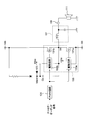
- FIG. 1 is a circuit diagram showing a configuration of a digital amplifier according to an embodiment of the present invention.
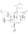
- Circuit diagram showing configuration of output stage of class D amplifier The circuit diagram which shows the structure of the digital amplifier of other embodiment which concerns on this invention.
- FIG. 1 is a circuit diagram showing a configuration of an output stage of a digital amplifier according to an embodiment of the present invention.
- the digital amplifier shown in FIG. 1 is a class D amplifier, and includes a PWM (Pulse Width Modulation) circuit 101, an amplifier circuit 103, a bootstrap capacitor Cb, a bootstrap control circuit 105, and a demodulation circuit 107.
- the digital amplifier of this embodiment is different from the class D amplifier shown in FIG. 3 in that a bootstrap control circuit 105 is provided.
- a speaker 111 is connected as a load to the output terminal 109 of the digital amplifier.
- each component provided in the digital amplifier of this embodiment will be described.
- the PWM circuit 101 performs pulse width modulation on an analog audio signal collected by a microphone (not shown) or an analog audio signal from various sound source sources and converts it into a digital pulse signal.
- the amplification circuit 103 includes FETs 131a and 131b connected in series in two upper and lower stages, and drive circuits 133a and 133b for driving the FETs.
- the lower (low side) drive circuit 133a controls switching of the low side FET 131a
- the upper (high side) drive circuit 133b controls switching of the high side FET 131b.
- the amplifier circuit 103 amplifies the digital pulse signal output from the PWM circuit 101 by alternately turning on and off these two upper and lower FETs 131a and 131b.
- the positive power supply Vcc (+ Vcc) is supplied to the drive circuit 133a on the low side.
- the positive power supply Vcc is a voltage required for the drive circuit 133a to turn on the FET 131a, and is, for example, “ ⁇ Vb + ⁇ ” (V).
- ⁇ Vb is a negative power supply voltage
- ⁇ is, for example, +5 to +10 (V).
- the power supply of the boot voltage Vboot obtained by adding the output voltage of the bootstrap capacitor Cb to the positive power supply Vb (+ Vb) is supplied to the drive circuit 133b on the high side.
- the high-side FET 131b is turned on when the boot voltage Vboot is equal to or higher than “+ Vb + ⁇ ” (V).
- the bootstrap capacitor Cb is a capacitor for bootstrapping the power supplied to the drive circuit 133b on the high side. Note that one end of the bootstrap capacitor Cb is connected to the drive circuit 133 b on the high side, and the other end is connected to the output of the amplifier circuit 103.
- the bootstrap control circuit 105 includes a resistor R1, a Zener diode Dz, Darlington-connected transistors Tr1 and Tr2, a diode D1, and a resistor R2.
- the resistor R1 and the Zener diode Dz are connected in series between the positive power source of the power source voltage (+ Vb) and the output of the amplifier circuit 103.
- the resistor R2, Darlington-connected transistors Tr1 and Tr2, and the diode D1 are connected in series between the positive power supply of the power supply voltage (+ Vb) and the bootstrap capacitor Cb. Further, as shown in FIG. 1, the cathode of the Zener diode Dz is connected to the base of the first-stage transistor Tr1.
- the operation of the bootstrap control circuit 105 when the digital amplifier according to this embodiment is started will be described.
- the digital amplifier according to this embodiment is activated, when the low-side FET 131a is turned on, the output voltage Vo of the amplifier circuit 103 is ⁇ Vb.
- the bootstrap capacitor Cb is charged until the boot voltage Vboot reaches the threshold value “Vz ⁇ 2Vbe ⁇ Vf” (at this time, the positive power supply ( (+ Vcc) is not sufficiently high, so the bootstrap capacitor Cb is not charged from the positive power supply (+ Vcc).
- Vz is a voltage on the cathode side of the Zener diode Dz, and is a voltage that is dropped from the positive power supply voltage (+ Vb) by the resistor R1.
- Vbe is the base-emitter voltage of the transistors Tr1 and Tr2.
- Vf is a forward voltage of the diode D1. Further, the charging current of the bootstrap capacitor Cb depends on the resistance value of the resistor R2.
- the bootstrap capacitor Cb When the positive power supply (+ Vcc) reaches a sufficiently high voltage, the bootstrap capacitor Cb is charged from the positive power supply (+ Vcc), and when the boot voltage Vboot reaches the threshold value “Vz ⁇ 2Vbe ⁇ Vf”, a Darlington connection is established.
- the transistors Tr1 and Tr2 are turned off when the base-emitter voltage becomes Vbe or less, and the current path from the positive power supply of the power supply voltage (+ Vb) to the bootstrap capacitor Cb is cut off.
- the boot voltage Vboot reaches the threshold value “Vz ⁇ 2Vbe ⁇ Vf”
- the charging of the bootstrap capacitor Cb is stopped.
- the digital amplifier according to this embodiment when the digital amplifier according to this embodiment is activated, when the high-side FET 131b is turned on, the output voltage of the bootstrap capacitor Cb is not sufficient, and the boot voltage Vboot is less than “+ Vb + ⁇ ” (V).
- the high-side drive circuit 133b cannot drive the FET 131b on.
- the two FETs 131a and 131b are both in the off state, and the output voltage Vo of the amplifier circuit 103 becomes a value close to 0 (V). Therefore, the bootstrap capacitor Cb is charged because it does not satisfy “Vz ⁇ 2Vbe ⁇ Vf”.
- the demodulating circuit 107 is composed of an LC circuit, and demodulates the digital pulse signal amplified by the amplifying circuit 103 and converts it into an analog audio signal.
- the analog audio signal converted by the demodulation circuit 107 is output from the speaker 111 via the output terminal 109.
- the bootstrap capacitor Cb is immediately after startup even when the digital amplifier is started up, even when the high-side FET 131b of the amplifier circuit 103 is turned on. Since the battery is charged, the high-side drive circuit 133b can turn on the FET 131b.
- This function is realized by the bootstrap control circuit 105.
- the control performed by the bootstrap control circuit 105 is charged according to the storage state of the bootstrap capacitor Cb, whether it is on-driven from the high-side FET 131b or the low-side FET 131a. It's as simple as doing.
- the digital amplifier when the digital amplifier is activated, the bootstrap capacitor can be reliably charged by simple control. As a result, the digital amplifier is reliably activated.
- the bootstrap control circuit 105 stops charging. Therefore, the power consumption of the digital amplifier can be reduced.
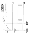
- the boot voltage Vboot is lowered as shown in FIG.
- the bootstrap control circuit 105 charges the bootstrap capacitor Cb again. The output voltage of the bootstrap capacitor Cb charged in this way can compensate for the decrease in the boot voltage Vboot.
- the amplifier circuit 103 includes the FETs 131a and 131b configured in two upper and lower stages, but may be a bipolar transistor or an IGBT.
- the bootstrap capacitor Cb and the bootstrap control circuit 105 are provided for the drive circuit 133b on the high side, but similar means may be provided on the low side as shown in FIG. .
- the voltage detection means (corresponding to the Zener diode Dz) shown in FIG. 4 may detect the voltage supplied to the low-side drive circuit 133a, as indicated by the dotted line.
- the digital amplifier is described as including the PWM circuit 101 and the demodulation circuit 107. However, these may be configured as a unit separate from the digital amplifier.
- the present invention is useful as a digital amplifier or the like that charges a bootstrap capacitor at startup.
Landscapes
- Engineering & Computer Science (AREA)
- Power Engineering (AREA)
- Amplifiers (AREA)
Priority Applications (1)
| Application Number | Priority Date | Filing Date | Title |
|---|---|---|---|
| CN201180008747.6A CN102754336B (zh) | 2010-02-08 | 2011-01-26 | 数字放大器 |
Applications Claiming Priority (2)
| Application Number | Priority Date | Filing Date | Title |
|---|---|---|---|
| JP2010025289A JP5484940B2 (ja) | 2010-02-08 | 2010-02-08 | デジタルアンプ |
| JP2010-025289 | 2010-02-08 |
Publications (1)
| Publication Number | Publication Date |
|---|---|
| WO2011096175A1 true WO2011096175A1 (ja) | 2011-08-11 |
Family
ID=44355194
Family Applications (1)
| Application Number | Title | Priority Date | Filing Date |
|---|---|---|---|
| PCT/JP2011/000428 Ceased WO2011096175A1 (ja) | 2010-02-08 | 2011-01-26 | デジタルアンプ |
Country Status (3)
| Country | Link |
|---|---|
| JP (1) | JP5484940B2 (enExample) |
| CN (1) | CN102754336B (enExample) |
| WO (1) | WO2011096175A1 (enExample) |
Cited By (6)
| Publication number | Priority date | Publication date | Assignee | Title |
|---|---|---|---|---|
| JP2016110874A (ja) * | 2014-12-08 | 2016-06-20 | パナソニックIpマネジメント株式会社 | 点灯装置及び照明器具 |
| WO2019160684A1 (en) * | 2018-02-19 | 2019-08-22 | Cirrus Logic International Semiconductor Ltd. | Dual bootstrapping for an open-loop pulse width modulation driver |
| GB2585794A (en) * | 2018-02-19 | 2021-01-20 | Cirrus Logic Int Semiconductor Ltd | Dual bootstrapping for an open-loop pulse width modulation driver |
| GB2593279A (en) * | 2020-02-07 | 2021-09-22 | Cirrus Logic Int Semiconductor Ltd | Dual bootstrapping for an open-loop pulse width modulation driver |
| US11190168B2 (en) | 2018-02-19 | 2021-11-30 | Cirrus Logic, Inc. | Dual bootstrapping for an open-loop pulse width modulation driver |
| EP4210224A4 (en) * | 2020-09-01 | 2024-10-09 | OMRON Corporation | SWITCHING CIRCUIT DEVICE AND POWER CONVERSION DEVICE |
Families Citing this family (4)
| Publication number | Priority date | Publication date | Assignee | Title |
|---|---|---|---|---|
| JP5582115B2 (ja) * | 2011-09-05 | 2014-09-03 | 三菱電機株式会社 | ブートストラップ回路、半導体装置 |
| CN104410289B (zh) * | 2014-11-28 | 2017-04-19 | 南京航空航天大学 | 一种双级式矩阵变换器驱动电源电路 |
| CN106714032B (zh) * | 2015-11-18 | 2020-02-04 | 晶豪科技股份有限公司 | 具有自举电容充电电路的电子装置 |
| JP2021084337A (ja) * | 2019-11-28 | 2021-06-03 | セイコーエプソン株式会社 | 液体吐出装置、及び駆動回路 |
Citations (2)
| Publication number | Priority date | Publication date | Assignee | Title |
|---|---|---|---|---|
| JP2004228912A (ja) * | 2003-01-22 | 2004-08-12 | Matsushita Electric Ind Co Ltd | 高効率電力増幅装置 |
| JP2008092730A (ja) * | 2006-10-04 | 2008-04-17 | Denso Corp | 負荷駆動回路 |
Family Cites Families (5)
| Publication number | Priority date | Publication date | Assignee | Title |
|---|---|---|---|---|
| JP2002330064A (ja) * | 2001-04-27 | 2002-11-15 | Onkyo Corp | ブートストラップ回路 |
| JP2003133924A (ja) * | 2001-10-19 | 2003-05-09 | Ematic:Kk | ハイサイドスイッチ駆動電源 |
| JP2006180049A (ja) * | 2004-12-21 | 2006-07-06 | Yamaha Corp | ディジタルアンプ |
| US8022682B2 (en) * | 2006-05-01 | 2011-09-20 | International Rectifier Corporation | Method to reduce inrush voltage and current in a switching power converter |
| JP5094431B2 (ja) * | 2008-01-11 | 2012-12-12 | ローム株式会社 | 電力増幅回路 |
-
2010
- 2010-02-08 JP JP2010025289A patent/JP5484940B2/ja active Active
-
2011
- 2011-01-26 WO PCT/JP2011/000428 patent/WO2011096175A1/ja not_active Ceased
- 2011-01-26 CN CN201180008747.6A patent/CN102754336B/zh active Active
Patent Citations (2)
| Publication number | Priority date | Publication date | Assignee | Title |
|---|---|---|---|---|
| JP2004228912A (ja) * | 2003-01-22 | 2004-08-12 | Matsushita Electric Ind Co Ltd | 高効率電力増幅装置 |
| JP2008092730A (ja) * | 2006-10-04 | 2008-04-17 | Denso Corp | 負荷駆動回路 |
Cited By (9)
| Publication number | Priority date | Publication date | Assignee | Title |
|---|---|---|---|---|
| JP2016110874A (ja) * | 2014-12-08 | 2016-06-20 | パナソニックIpマネジメント株式会社 | 点灯装置及び照明器具 |
| WO2019160684A1 (en) * | 2018-02-19 | 2019-08-22 | Cirrus Logic International Semiconductor Ltd. | Dual bootstrapping for an open-loop pulse width modulation driver |
| GB2585794A (en) * | 2018-02-19 | 2021-01-20 | Cirrus Logic Int Semiconductor Ltd | Dual bootstrapping for an open-loop pulse width modulation driver |
| US11070203B2 (en) | 2018-02-19 | 2021-07-20 | Cirrus Logic, Inc. | Dual bootstrapping for an open-loop pulse width modulation driver |
| US11190168B2 (en) | 2018-02-19 | 2021-11-30 | Cirrus Logic, Inc. | Dual bootstrapping for an open-loop pulse width modulation driver |
| GB2585794B (en) * | 2018-02-19 | 2022-04-20 | Cirrus Logic Int Semiconductor Ltd | Dual bootstrapping for an open-loop pulse width modulation driver |
| GB2593279A (en) * | 2020-02-07 | 2021-09-22 | Cirrus Logic Int Semiconductor Ltd | Dual bootstrapping for an open-loop pulse width modulation driver |
| EP4210224A4 (en) * | 2020-09-01 | 2024-10-09 | OMRON Corporation | SWITCHING CIRCUIT DEVICE AND POWER CONVERSION DEVICE |
| US12160230B2 (en) | 2020-09-01 | 2024-12-03 | Omron Corporation | Switching circuit apparatus capable of controlling multiple switching elements to synchronously turn on and off with bootstrap circuit |
Also Published As
| Publication number | Publication date |
|---|---|
| CN102754336A (zh) | 2012-10-24 |
| CN102754336B (zh) | 2015-05-20 |
| JP2011166346A (ja) | 2011-08-25 |
| JP5484940B2 (ja) | 2014-05-07 |
Similar Documents
| Publication | Publication Date | Title |
|---|---|---|
| JP5484940B2 (ja) | デジタルアンプ | |
| CN103199677B (zh) | 单路隔离型mosfet驱动电路 | |
| US8072202B2 (en) | Gate driver in buck converters | |
| US8022682B2 (en) | Method to reduce inrush voltage and current in a switching power converter | |
| CN110212757B (zh) | 功率转换电路和功率转换方法 | |
| US10879885B2 (en) | Diode circuit | |
| JP5229495B2 (ja) | スイッチング装置及びその制御方法 | |
| US20090167419A1 (en) | Voltage converting circuit | |
| JP2014212651A (ja) | 変換装置 | |
| JP5191672B2 (ja) | スイッチングアンプ | |
| JP2002330064A (ja) | ブートストラップ回路 | |
| JP2006080024A (ja) | 放電灯点灯装置 | |
| JP2001308688A (ja) | 出力回路 | |
| CN105144557B (zh) | 转换装置 | |
| JP2008042633A (ja) | 電圧制御型スイッチング素子の共振ゲート駆動回路 | |
| JP4319336B2 (ja) | Mosスイッチング回路 | |
| JP2020188673A (ja) | 電気回路及び電源装置 | |
| JP2005217497A (ja) | 半導体集積回路装置用負荷駆動回路 | |
| JP5009083B2 (ja) | スイッチング電源回路 | |
| JP4161901B2 (ja) | 昇圧回路および負荷駆動回路 | |
| JP7115204B2 (ja) | 駆動用電源生成回路 | |
| JP2005210848A (ja) | 直流電圧変換装置 | |
| JP2016063648A (ja) | 駆動装置 | |
| WO2007015520A1 (ja) | 電源装置 | |
| TW201630318A (zh) | 開關電路 |
Legal Events
| Date | Code | Title | Description |
|---|---|---|---|
| WWE | Wipo information: entry into national phase |
Ref document number: 201180008747.6 Country of ref document: CN |
|
| 121 | Ep: the epo has been informed by wipo that ep was designated in this application |
Ref document number: 11739526 Country of ref document: EP Kind code of ref document: A1 |
|
| DPE1 | Request for preliminary examination filed after expiration of 19th month from priority date (pct application filed from 20040101) | ||
| NENP | Non-entry into the national phase |
Ref country code: DE |
|
| 122 | Ep: pct application non-entry in european phase |
Ref document number: 11739526 Country of ref document: EP Kind code of ref document: A1 |